EP1267491A2 - Precision low jitter oscillator circuit - Google Patents
Precision low jitter oscillator circuit Download PDFInfo
- Publication number
- EP1267491A2 EP1267491A2 EP02008038A EP02008038A EP1267491A2 EP 1267491 A2 EP1267491 A2 EP 1267491A2 EP 02008038 A EP02008038 A EP 02008038A EP 02008038 A EP02008038 A EP 02008038A EP 1267491 A2 EP1267491 A2 EP 1267491A2
- Authority
- EP
- European Patent Office
- Prior art keywords
- pair
- oscillator
- differential
- coupled
- digital
- Prior art date
- Legal status (The legal status is an assumption and is not a legal conclusion. Google has not performed a legal analysis and makes no representation as to the accuracy of the status listed.)
- Granted
Links
Images
Classifications
-
- H—ELECTRICITY
- H04—ELECTRIC COMMUNICATION TECHNIQUE
- H04R—LOUDSPEAKERS, MICROPHONES, GRAMOPHONE PICK-UPS OR LIKE ACOUSTIC ELECTROMECHANICAL TRANSDUCERS; DEAF-AID SETS; PUBLIC ADDRESS SYSTEMS
- H04R25/00—Deaf-aid sets, i.e. electro-acoustic or electro-mechanical hearing aids; Electric tinnitus maskers providing an auditory perception
- H04R25/50—Customised settings for obtaining desired overall acoustical characteristics
- H04R25/505—Customised settings for obtaining desired overall acoustical characteristics using digital signal processing
-
- H—ELECTRICITY
- H03—ELECTRONIC CIRCUITRY
- H03K—PULSE TECHNIQUE
- H03K3/00—Circuits for generating electric pulses; Monostable, bistable or multistable circuits
- H03K3/02—Generators characterised by the type of circuit or by the means used for producing pulses
- H03K3/023—Generators characterised by the type of circuit or by the means used for producing pulses by the use of differential amplifiers or comparators, with internal or external positive feedback
- H03K3/0231—Astable circuits
-
- H—ELECTRICITY
- H03—ELECTRONIC CIRCUITRY
- H03K—PULSE TECHNIQUE
- H03K3/00—Circuits for generating electric pulses; Monostable, bistable or multistable circuits
- H03K3/02—Generators characterised by the type of circuit or by the means used for producing pulses
- H03K3/027—Generators characterised by the type of circuit or by the means used for producing pulses by the use of logic circuits, with internal or external positive feedback
- H03K3/03—Astable circuits
- H03K3/0315—Ring oscillators
- H03K3/0322—Ring oscillators with differential cells
-
- H—ELECTRICITY
- H03—ELECTRONIC CIRCUITRY
- H03K—PULSE TECHNIQUE
- H03K5/00—Manipulating of pulses not covered by one of the other main groups of this subclass
- H03K5/13—Arrangements having a single output and transforming input signals into pulses delivered at desired time intervals
- H03K5/133—Arrangements having a single output and transforming input signals into pulses delivered at desired time intervals using a chain of active delay devices
-
- H—ELECTRICITY
- H03—ELECTRONIC CIRCUITRY
- H03K—PULSE TECHNIQUE
- H03K5/00—Manipulating of pulses not covered by one of the other main groups of this subclass
- H03K2005/00013—Delay, i.e. output pulse is delayed after input pulse and pulse length of output pulse is dependent on pulse length of input pulse
- H03K2005/00019—Variable delay
- H03K2005/00058—Variable delay controlled by a digital setting
- H03K2005/00071—Variable delay controlled by a digital setting by adding capacitance as a load
-
- H—ELECTRICITY
- H03—ELECTRONIC CIRCUITRY
- H03K—PULSE TECHNIQUE
- H03K5/00—Manipulating of pulses not covered by one of the other main groups of this subclass
- H03K2005/00013—Delay, i.e. output pulse is delayed after input pulse and pulse length of output pulse is dependent on pulse length of input pulse
- H03K2005/0015—Layout of the delay element
- H03K2005/00195—Layout of the delay element using FET's
- H03K2005/00208—Layout of the delay element using FET's using differential stages
Definitions
- This invention generally relates to oscillator circuits. More specifically, the invention provides a precision, low jitter oscillator circuit that is particularly well-suited for generating clock signals used in digital systems, such as a digital hearing aid system. The invention provides utility, however, in any circuit application that requires a precision, low jitter clock source.
- Oscillators for generating clock signals are known.
- the two most common types of oscillators are crystal oscillators and ring oscillators.
- a crystal oscillator is a piezo-electric device that resonates at a particular frequency when a voltage is applied to the crystal. Although some crystals can provide low jitter performance, the mechanical dimensions of the crystal typically limit its applicability in miniaturized circuitry, such as digital hearing aids, implantable bio-electric devices and probes, and/or any other miniature electronic device.
- Ring oscillators are generally composed of a plurality of logic gates.
- the logic gates are typically differential inverters that are configured in a feedback loop in order to provide an oscillation output signal.
- the cumulative delay through the plurality of differential inverters determines the frequency of the oscillation output signal.
- These differential inverters typically employ active loads (i.e., transistor devices) in their output stages.
- the active loads limit the low jitter performance of the oscillator such that to achieve low jitter on the output clock signal, the differential inverters must be operated with a relatively high supply voltage, such as 3 to 5 volts.
- Miniaturized circuitry typically includes only a low voltage supply, such as a 1.3 volt single battery supply, and thus these known oscillators are of limited utility.
- these active-load differential inverters typically employ an adjustable current source, which further adds to the power consumption of the circuitry.
- ring oscillators employing differential inverters with active loads have been difficult to integrate into a miniaturized circuit application. ( See, for example , A. Hajimire, S. Limotyrakis, and T.H. Lee, “Jitter and Phase Noise in Ring Oscillators ,” IEEE Journal of Solid-State Circuits, Vol. 34, No. 6, June 1999, pp. 790-804)
- a digital hearing aid system needs an oscillator as a clock reference.
- the clock must have low jitter to ensure a high signal-to-noise ratio ("S/N") of both the analog-to-digital (“A/D”) converter, and also the digital-to-analog (“D/A”) converter that are typically included in the hearing aid.
- S/N signal-to-noise ratio
- A/D analog-to-digital
- D/A digital-to-analog
- Power consumption in this type of system should be minimized since the entire device is typically powered from a 1.3 volt zinc-air hearing aid battery.
- Other requirements of this type of system include small size and clock precision.
- a precision, low jitter oscillator circuit is provided that is particularly well-suited for generating a clock signal in miniature digital systems, such as digital hearing aids.
- the oscillator includes a plurality of differential inverters configured in a feedback loop to generate an oscillating clock signal.
- the differential inverters include a capacitive trimming network for adjusting the frequency of the oscillating clock signal and employ resistive loads for minimizing jitter in the clock signal.
- the components of the oscillator are fabricated in a common silicon process to minimize the size of the oscillator.
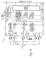
- FIG. 1 is a block diagram of an exemplary digital hearing aid system 12 incorporating a precision, low jitter oscillator circuit 26 according to the present invention. It should be understood, however, that this digital hearing aid system 12 is just one of many applications for the precision, low jitter oscillator circuit 26 described herein.
- the digital hearing aid system 12 includes several external components 14, 16, 18, 20, 22, 24, 26, 28, and, preferably, a single integrated circuit (IC) 12A.
- the external components include a pair of microphones 24, 26, a tele-coil 28, a volume control potentiometer 24, a memory-select toggle switch 16, battery terminals 18, 22, and a speaker 20.
- Sound is received by the pair of microphones 24, 26, and converted into electrical signals that are coupled to the FMIC 12C and RMIC 12D inputs to the IC 12A.
- FMIC refers to "front microphone”
- RMIC refers to "rear microphone.”
- the microphones 24, 26 are biased between a regulated voltage output from the RREG and FREG pins 12B, and the ground nodes FGND 12F, RGND 12G.
- the regulated voltage output on FREG and RREG is generated internally to the IC 12A by regulator 30.
- the tele-coil 28 is a device used in a hearing aid that magnetically couples to a telephone handset and produces an input current that is proportional to the telephone signal. This input current from the tele-coil 28 is coupled into the rear microphone A/D converter 32B on the IC 12A when the switch 76 is connected to the "T" input pin 12E, indicating that the user of the hearing aid is talking on a telephone.
- the tele-coil 28 is used to prevent acoustic feedback into the system when talking on the telephone.
- the volume control potentiometer 14 is coupled to the volume control input 12N of the IC 12A. This variable resistor is used to set the volume sensitivity of the digital hearing aid.
- the memory-select toggle switch 16 is coupled between the positive voltage supply VB 18 to the IC 12A and the memory-select input pin 12L.
- This switch 16 is used to toggle the digital hearing aid system 12 between a series of setup configurations.
- the device may have been previously programmed for a variety of environmental settings, such as quiet listening, listening to music, a noisy setting, etc.
- the system parameters of the IC 12A may have been optimally configured for the particular user.
- the toggle switch 16 By repeatedly pressing the toggle switch 16, the user may then toggle through the various configurations stored in the read-only memory 44 of the IC 12A.
- the battery terminals 12K, 12H of the IC 12A are preferably coupled to a single 1.3 volt zinc-air battery. This battery provides the primary power source for the digital hearing aid system.
- the last external component is the speaker 20.
- This element is coupled to the differential outputs at pins 12J, 12I of the IC 12A, and converts the processed digital input signals from the two microphones 24, 26 into an audible signal for the user of the digital hearing aid system 12.
- a pair of A/D converters 32A, 32B are coupled between the front and rear microphones 24, 26, and the sound processor 38, and convert the analog input signals into the digital domain for digital processing by the sound processor 38.
- a single D/A converter 48 converts the processed digital signals back into the analog domain for output by the speaker 20.
- Other system elements include a regulator 30, a volume control A/D 40, an interface/system controller 42, an EEPROM memory 44, a power-on reset circuit 46, and a oscillator/system clock 36.
- the oscillator/system clock 36 is discussed in more detail below with respect to FIGs. 2-6.
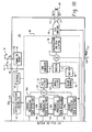
- the sound processor 38 preferably includes a directional processor 50, a pre-filter 52, a wide-band twin detector 54, a band-split filter 56, a plurality of narrow-band channel processing and twin detectors 58A-58D, a summer 60, a post filter 62, a notch filter 64, a volume control circuit 66, an automatic gain control output circuit 68, a peak clipping circuit 70, a squelch circuit 72, and a tone generator 74.
- a directional processor 50 preferably includes a directional processor 50, a pre-filter 52, a wide-band twin detector 54, a band-split filter 56, a plurality of narrow-band channel processing and twin detectors 58A-58D, a summer 60, a post filter 62, a notch filter 64, a volume control circuit 66, an automatic gain control output circuit 68, a peak clipping circuit 70, a squelch circuit 72, and a tone generator 74.
- the sound processor 38 processes digital sound as follows. Sound signals input to the front and rear microphones 24, 26 are coupled to the front and rear A/D converters 32A, 32B, which are preferably Sigma-Delta modulators followed by decimation filters that convert the analog sound inputs from the two microphones into a digital equivalent. Note that when a user of the digital hearing aid system is talking on the telephone, the rear A/D converter 32B is coupled to the tele-coil input "T" 12E via switch 76. Both of the front and rear A/D converters 32A, 32B are clocked with the output clock signal from the oscillator/system clock 36 (discussed in more detail below). This same output clock signal is also coupled to the sound processor 38 and the D/A converter 48.
- the front and rear A/D converters 32A, 32B are preferably Sigma-Delta modulators followed by decimation filters that convert the analog sound inputs from the two microphones into a digital equivalent. Note that when a user of the digital hearing aid system is talking on the telephone
- the front and rear digital sound signals from the two A/D converters 32A, 32B are coupled to the directional processor and headroom expander 50 of the sound processor 38.
- the rear A/D converter 32B is coupled to the processor 50 through switch 75. In a first position, the switch 75 couples the digital output of the rear A/D converter 32 B to the processor 50, and in a second position, the switch 75 couples the digital output of the rear A/D converter 32B to summation block 71 for the purpose of compensating for occlusion.
- Occlusion is the amplification of the users own voice within the ear canal.
- the rear microphone can be moved inside the ear canal to receive this unwanted signal created by the occlusion effect.
- the occlusion effect is usually reduced in these types of systems by putting a mechanical vent in the hearing aid. This vent, however, can cause an oscillation problem as the speaker signal feeds back to the microphone(s) through the vent aperture.
- the system shown in FIG. 1 solves this problem by canceling the unwanted signal received by the rear microphone 26 by feeding forward the rear signal from the A/D converter 32B to summation circuit 71.
- the summation circuit 71 then subtracts the unwanted signal from the processed composite signal to thereby compensate for the occlusion effect.
- the directional processor and headroom expander 50 includes a combination of filtering and delay elements that, when applied to the two digital input signals, forms a single, directionally-sensitive response. This directionally-sensitive response is generated such that the gain of the directional processor 50 will be a maximum value for sounds coming from the front microphone 24 and will be a minimum value for sounds coming from the rear microphone 26.
- the headroom expander portion of the processor 50 significantly extends the dynamic range of the A/D conversion, which is very important for high fidelity audio signal processing. It does this by dynamically adjusting the A/D converters 32A/32B operating points.
- the headroom expander 50 adjusts the gain before and after the A/D conversion so that the total gain remains unchanged, but the intrinsic dynamic range of the A/D converter block 32A/32B is optimized to the level of the signal being processed.
- the output from the directional processor and headroom expander 50 is coupled to a pre-filter 52, which is a general-purpose filter for pre-conditioning the sound signal prior to any further signal processing steps.
- This "pre-conditioning" can take many forms, and, in combination with corresponding "post-conditioning" in the post filter 62, can be used to generate special effects that may be suited to only a particular class of users.
- the pre-filter 52 could be configured to mimic the transfer function of the user's middle ear, effectively putting the sound signal into the "cochlear domain.”
- Signal processing algorithms to correct a hearing impairment based on, for example, inner hair cell loss and outer hair cell loss, could be applied by the sound processor 38.
- the post-filter 62 could be configured with the inverse response of the pre-filter 52 in order to convert the sound signal back into the "acoustic domain" from the "cochlear domain.”
- the post-filter 62 could be configured with the inverse response of the pre-filter 52 in order to convert the sound signal back into the "acoustic domain" from the "cochlear domain.”
- other pre-conditioning/post-conditioning configurations and corresponding signal processing algorithms could be utilized.
- the pre-conditioned digital sound signal is then coupled to the band-split filter 56, which preferably includes a bank of filters with variable corner frequencies and pass-band gains. These filters are used to split the single input signal into four distinct frequency bands.
- the four output signals from the band-split filter 56 are preferably in-phase so that when they are summed together in block 60, after channel processing, nulls or peaks in the composite signal (from the summer) are minimized.
- Channel processing of the four distinct frequency bands from the band-split filter 56 is accomplished by a plurality of channel processing/twin detector blocks 58A-58D. Although four blocks are shown in FIG. 1, it should be clear that more than four (or less than four) frequency bands could be generated in the band-split filter 56, and thus more or less than four channel processing/twin detector blocks 58 may be utilized with the system.
- Each of the channel processing/twin detectors 58A-58D provide an automatic gain control (“AGC”) function that provides compression and gain on the particular frequency band (channel) being processed. Compression of the channel signals permits quieter sounds to be amplified at a higher gain than louder sounds, for which the gain is compressed. In this manner, the user of the system can hear the full range of sounds since the circuits 58A-58D compress the full range of normal hearing into the reduced dynamic range of the individual user as a function of the individual user's hearing loss within the particular frequency band of the channel.
- AGC automatic gain control
- the channel processing blocks 58A-58D can be configured to employ a twin detector average detection scheme while compressing the input signals.
- This twin detection scheme includes both slow and fast attack/release tracking modules that allow for fast response to transients (in the fast tracking module), while preventing annoying pumping of the input signal (in the slow tracking module) that only a fast time constant would produce.
- the outputs of the fast and slow tracking modules are compared, and the compression slope is then adjusted accordingly.
- the compression ratio, channel gain, lower and upper thresholds (return to linear point), and the fast and slow time constants (of the fast and slow tracking modules) can be independently programmed and saved in memory 44 for each of the plurality of channel processing blocks 58A-58D.
- FIG. 1 also shows a communication bus 59, which may include one or more connections, for coupling the plurality of channel processing blocks 58A-58D.
- This inter-channel communication bus 59 can be used to communicate information between the plurality of channel processing blocks 58A-58D such that each channel (frequency band) can take into account the "energy” level (or some other measure) from the other channel processing blocks.
- each channel processing block 58A-58D would take into account the "energy” level from the higher frequency channels.
- the "energy" level from the wide-band detector 54 may be used by each of the relatively narrow-band channel processing blocks 58A-58D when processing their individual input signals.
- the four channel signals are summed by summer 60 to form a composite signal.
- This composite signal is then coupled to the post-filter 62, which may apply a post-processing filter function as discussed above.
- the composite signal is then applied to a notch-filter 64, that attenuates a narrow band of frequencies that is adjustable in the frequency range where hearing aids tend to oscillate.
- This notch filter 64 is used to reduce feedback and prevent unwanted "whistling" of the device.
- the notch filter 64 may include a dynamic transfer function that changes the depth of the notch based upon the magnitude of the input signal.
- the composite signal is then coupled to a volume control circuit 66.
- the volume control circuit 66 receives a digital value from the volume control A/D 40, which indicates the desired volume level set by the user via potentiometer 14, and uses this stored digital value to set the gain of an included amplifier circuit.
- the composite signal is then coupled to the AGC-output block 68.
- the AGC-output circuit 68 is a high compression ratio, low distortion limiter that is used to prevent pathological signals from causing large scale distorted output signals from the speaker 20 that could be painful and annoying to the user of the device.
- the composite signal is coupled from the AGC-output circuit 68 to a squelch circuit 72, that performs an expansion on low-level signals below an adjustable threshold.
- the squelch circuit 72 uses an output signal from the wide-band detector 54 for this purpose. The expansion of the low-level signals attenuates noise from the microphones and other circuits when the input S/N ratio is small, thus producing a lower noise signal during quiet situations.
- a tone generator block 74 is also shown coupled to the squelch circuit 72, which is included for calibration and testing of the system.
- the output of the squelch circuit 72 is coupled to one input of summer 71.
- the other input to the summer 71 is from the output of the rear A/D converter 32B, when the switch 75 is in the second position.
- These two signals are summed in summer 71, and passed along to the interpolator and peak clipping circuit 70.
- This circuit 70 also operates on pathological signals, but it operates almost instantaneously to large peak signals and is high distortion limiting.
- the interpolator shifts the signal up in frequency as part of the D/A process and then the signal is clipped so that the distortion products do not alias back into the baseband frequency range.
- the output of the interpolator and peak clipping circuit 70 is coupled from the sound processor 38 to the D/A H-Bridge 48.
- This circuit 48 converts the digital representation of the input sound signals to a pulse density modulated representation with complimentary outputs. These outputs are coupled off-chip through outputs 12J, 121 to the speaker 20, which low-pass filters the outputs and produces an acoustic analog of the output signals.
- the D/A H-Bridge 48 includes an interpolator, a digital Delta-Sigma modulator, and an H-Bridge output stage.
- the D/A H-Bridge 48 is also coupled to and receives the clock signal from the oscillator/system clock 36 (described below).
- the interface/system controller 42 is coupled between a serial data interface pin 12M on the IC 12, and the sound processor 38. This interface is used to communicate with an external controller for the purpose of setting the parameters of the system. These parameters can be stored on-chip in the EEPROM 44. If a "black-out” or “brown-out” condition occurs, then the power-on reset circuit 46 can be used to signal the interface/system controller 42 to configure the system into a known state. Such a condition can occur, for example, if the battery fails.
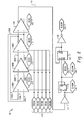
- FIG. 2 is a circuit schematic of an exemplary precision, low jitter oscillator circuit 36 according to the present invention.
- This oscillator circuit can be used, for example, as the oscillator/system clock 36 shown in FIG. 1 for the digital hearing aid system.
- the preferred oscillator 36 includes a plurality of differential inverters 100A-100C, which are configured in a feedback loop to generate an oscillation signal, a differential-to-single-ended comparator 102, an inverter 114, a first D flip-flop 116, a second D flip-flop 122, and an inverter 126.
- Each of the differential inverters 100A-100C includes a pair of inputs 104A/106A to 104C/106C and a pair of outputs 104B/106B to 104D/106D.
- the outputs from the third differential inverter 100C are fed back as the inputs to the first differential inverter 100A, which results in an oscillating output signal pair 104D/106D.
- the preferred differential inverter circuit 100A-100C is described below in connection with FIGs. 3-4.
- the differential inverters 100A-100C each comprise a delay stage in the oscillator. The time duration of this delay determines the oscillation frequency of the oscillator. Although three delay stages 100A-100C are shown in FIG. 2, the oscillator could have more than three stages. Each of the delay stages 100A-100C and the comparator circuit 102 are biased using a common bias signal 112 that is generated by the bias circuit shown in FIG. 5.
- a digital trimming word 110 comprising a plurality of digital trimming bits (TRIM0 - TRIM4). As described in more detail below, these digital trimming bits are used to alter the delay of the differential inverters 100A-100C, and thus alter the oscillation frequency of the oscillator.
- the differential oscillation output signals 104D/106D are coupled to the comparator 102, which converts the differential oscillation output signals into a single-ended oscillation output signal 108.
- This signal 108 is then coupled to an inverter 114, which further amplifies the oscillation signal 108.
- the output of this inverter 114 is a node labeled "CLK8M,” indicating that the oscillator is preferably set to generate an 8 MHz output clock signal.
- the first D flip flop 116 is configured to divide the 8 MHz clock in two in order to generate a 4 MHz clock signal, at node "CLK4M.” This 4 MHz signal is further divided by two in the second D flip flop 122 to generate a 2 MHz clock signal "CLK2M,” which is used by the A/D and D/A converters 32A, 32B, 48 in the digital hearing aid shown in FIG. 1.
- the second D flip flop 122 also receives a reset signal "RSTB" from a controller. The reset signal is used to synchronize the 2 MHz clock with other external clock signals in the system.
- RSTB reset signal
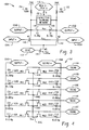
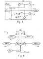
- FIG. 3 is a circuit schematic of an exemplary differential inverter stage 100A having a digital capacitive trimming network 150 for use with the precision, low jitter oscillator circuit shown in FIG. 2.
- the differential inverter stage 100A includes a pair of input NMOS transistors M1 140, M2 142, a biasing NMOS device M5 144, a pair of base delay capacitors C1, C2 146, 148, a pair of resistor loads R1, R2 154, 152, and a digital capacitive trimming network 150.
- the two NMOS transistors M1, M2 are source-coupled to the drain of NMOS transistor M5, which generates a constant bias current that is split among M1 and M2.
- the constant bias current is determined by the bias voltage level 112 input to the gate of NMOS device M5 from the bias circuit, shown in FIG. 5.
- the gate of M1 is coupled to the positive input node 104A, and the gate of M2 is coupled to the negative input node 106A.
- the drain of M1 is coupled to the negative output node 104B, and the drain of M2 is coupled to the positive output node 106B.
- output nodes 106B, 104B are coupled together via the base delay capacitors C1, C2 146, 148, and the capacitive trimming network 150, described in more detail below in connection with FIG. 4.
- the output nodes 104B/106B are coupled to the Vdd power supply through resistive loads R1, R2 154, 152.
- the input transistors M1, M2 are preferably large area devices in order to reduce 1/f noise, and employ large width/length ("W/L") ratios on the gate structure in order to increase transconductance.
- the large size of these devices also provides large parasitic capacitance, which combine with the base delay capacitors C1, C2 146, 148.
- Load resistors R1 and R2 are monolithic resistors fabricated from the same silicon process that is used to make the NMOS devices, the capacitors, and all of the other circuit elements of the oscillator 36.
- these resistors R1, R2 are manufactured from narrow width, high-resistivity material (i.e., non-salicided polysilicon), with low parasitic capacitance.
- the load resistors determine the DC operating point of the inverter.
- resistive loads instead of active loads (i.e., PMOS transistors)
- the inverter 100A exhibits lower 1/f noise (which leads to improved low jitter) and improved precision.
- the capacitive trimming network 150 receives, as inputs, the digital trimming bits 110. As shown below in connection with FIG. 4, these digital trimming bits operate a series of NMOS pass transistors that connect a set of binary-weighted capacitors between the two output nodes 104B/106B to thereby alter the capacitance between the output nodes. The total capacitance between these two output nodes (C L ) determines the delay through the inverter, and thus the oscillation frequency of the oscillator ( f OSC ).
- Low jitter in the differential inverter is achieved by using resistive loads (instead of active loads), and by optimizing the design of the active devices and their signal swings.
- the transistors M1, M2 of the differential inverter 100A are preferably scaled so that the input and output levels of each stage 100A-100C are matched.
- the operating point of the inverter stage is optimized to maximize signal swing and to prevent triode operation of the transistors. Optimizing the signal swing in this manner improves the dv/dt performance of the inverter at a particular frequency so that input noise has minimum impact on jitter.
- FIG. 4 is a more detailed circuit schematic of an exemplary digital capacitive trimming network 150 used in the differential inverter stage shown in FIG. 3.
- This circuit 150 is coupled between the output nodes 104B/106B, and includes a plurality of binary weighted capacitors C11-C52, which are coupled between the output nodes 104B/106B via pass transistors M11-M52.
- the gates of the NMOS pass transistors are coupled to the digital trimming bits 110 (TRIM0 - TRIM4).
- the first level of binary weighted capacitors is the combination of C11 and C12. Each of these capacitors preferably contributes 0.014 picofarads of capacitance to the base capacitors C1, C2, which are preferably 0.18 picofarads.
- the first level capacitance is added to the base capacitance by asserting a positive logic level on trimming bit TRIM0 110E. When TRIM0 is positive, the pass transistors M11 and M12 are turned on, thus coupling the two capacitors together between the output nodes 104B/106B.
- the second, third, fourth and fifth levels of binary weighted capacitors operate to add capacitance between the output nodes 104B, 106B when the corresponding digital trimming bits are activated.
- the second level capacitors C21, C22 are 0.031 picofarads
- the third level capacitors C31, C32 are 0.065 picofarads
- the fourth level capacitors C41, C42 are 0.133 picofarads
- the fifth level capacitors C51, C52 are 0.269 picofarads.
- the five trimming bits provide a frequency adjustment of +/- 2.5% of nominal with a range of about + 114% to -45%. Although five digital trimming bits, and five sets of trimming capacitors are preferred, it should be understood that any number of trimming levels and trimming capacitor sets could be used with the present invention.
- the five trimming bits are configured to generate the nominal frequency of the oscillator. Preferably, this is somewhere between the eighth and twentieth level of the thirty-two possible levels for the trimming bits. In the preferred embodiment shown in FIGs. 1 and 2, this nominal frequency is 8 MHz. By configuring the trimming bits in this manner, the nominal frequency can be adjusted up and down from the nominal level.
- FIG. 5 is a more detailed circuit schematic of an exemplary bias circuit for use with the precision, low jitter oscillator circuit shown in FIG. 2.
- This circuit includes MOS devices 170-184 and resistor 186.
- the circuit is a constant-transconductance bias circuit with current mirrors connected in a pair of feedback loops.
- the bias voltage level 112 generated by this circuit is applied to the differential inverters 100A-100C and the comparator 102 in order to bias these circuits at the same operating point.
- MOS transistors M1-M4 180, 184, 174, 178 and resistor R 186 form the biasing circuitry.
- the channel length of these devices is selected in order to provide a high power-supply rejection ratio.
- MOS transistors Ms1, Ms2 and Ms3 170, 172, 176 form a simple start-up circuit for the bias-generating devices.
- Transistor Mc 182 is configured as a MOS capacitor, and is used to reduce the output noise of the bias voltage 112.
- FIG. 6 is a more detailed circuit schematic of an exemplary comparator circuit 102 for use with the precision, low jitter oscillator circuit shown in FIG. 2.
- the comparator circuit 102 is almost identical to the differential inverter 100A shown in FIG. 3, except that it does not include the capacitors C1, C2 or the capacitive trimming network 150. Although two outputs are shown in FIG. 6, when configured in the oscillator shown in FIG. 2, only the negative output signal 108 is operative in the circuit.
- the comparator also uses resistive loads R1, R2 in order to reduce 1/f noise, and thus minimize jitter.
- the present invention provides many advantages over prior oscillator circuits. Some of these advantages include: (1) no external parts; the components shown in FIGs. 2-4 are all manufactured from the same silicon process, thereby minimizing the size of the oscillator circuit; (2) high precision; by using the capacitive trimming networks, the oscillation frequency can be trimmed to within +/- 2.5% of the nominal frequency setting; and (3) low jitter; as explained above, by using resistive loads in the differential inverter, and by optimizing and matching the design of the active devices, jitter is minimized.
Abstract
Description
Claims (38)
- An oscillator, comprising:a plurality of differential inverters configured in a feedback loop to generate an oscillating output signal, each differential inverter including a capacitive trimming network; anda plurality of digital trimming bits coupled to the capacitive trimming networks for selecting one or more capacitors in each capacitive trimming network, wherein the delay of each differential inverter is simultaneously adjusted in response to the digital trimming bits.
- The oscillator of claim 1, further comprising:a comparator coupled to one of the differential inverters that converts the oscillating output signal from a differential signal to a single-ended signal.
- The oscillator of claim 2, further comprising:a first divider for dividing the single-ended signal by a factor of 2 to form a first divided signal.
- The oscillator of claim 3, further comprising:a second divider for dividing the first divided signal by a factor of 2 to form a second divided signal.
- The oscillator of claim 4, wherein the second divider is coupled to a reset signal and includes circuitry to synchronize the second divided signal with an external clock signal.
- The oscillator of claim 1, further comprising:a bias circuit coupled to the plurality of differential inverters for biasing the differential inverters at a common operating point.
- The oscillator of claim 1, wherein the differential inverters include a pair of inputs and a pair of outputs, an input stage transistor pair coupled between the pair of inputs and the pair of outputs, and a pair of resistive loads coupled to each output in the pair of outputs.
- The oscillator of claim 7, wherein the differential inverters further include a pair of base capacitors coupled between the pair of outputs, wherein the base capacitors set a base time delay for signals communicated through the differential inverter.
- The oscillator of claim 8, wherein the capacitive trimming network is coupled in parallel to the base capacitors between the pair of outputs.
- The oscillator of claim 9, wherein the differential inverters further include a biasing transistor coupled to an external bias signal and the pair of input transistors.
- The oscillator of claim 1, wherein the oscillating output signal is used to clock at least one A/D converter and at least one D/A converter in a digital hearing aid system.
- The oscillator of claim 1, wherein the plurality of differential inverters include at least three differential inverters.
- The oscillator of claim 2, further comprising:a bias circuit coupled to the plurality of differential inverters and the comparator for biasing the differential inverters and the comparator at a common operating point.
- The oscillator of claim 1, wherein the capacitive trimming networks include a plurality of binary weighted capacitors.
- The oscillator of claim 14, wherein the plurality of binary weighted capacitors are configured in a plurality of binary levels, each binary level including a pair of capacitors and at least one pass transistor, wherein the pass transistor is coupled to one of the digital trimming bits.
- The oscillator of claim 15, wherein the digital trimming bits turn on and off the pass transistors at each of the binary levels in order to selectively connect the pair of capacitors in each of the binary levels to the differential inverters.
- The oscillator of claim 16, wherein the plurality of binary levels includes at least five levels.
- The oscillator of claim 16, wherein the capacitive trimming networks are coupled to an output stage of the differential inverters.
- The oscillator of claim 7, wherein the pair of resistive loads and the input stage transistor pair are manufactured from a common semiconductor process.
- The oscillator of claim 19, wherein the pair of resistive loads are made of non-salicided polysilicon.
- The oscillator of claim 7, wherein the input stage transistor pair are NMOS devices.
- The oscillator of claim 1, wherein the frequency of the oscillating output signal is varied by selecting one or more of the digital trimming bits.
- The oscillator of claim 13, wherein the bias circuit is a constant transconductance bias circuit.
- The oscillator of claim 22, wherein the frequency of the oscillating output signal can be varied by about +/- 2.5% from a nominal frequency value via the digital trimming bits.
- A differential inverter, comprising:a pair of inputs and a pair of outputs;an input stage transistor pair coupled between the pair of inputs and the pair of outputs;a pair of resistive loads coupled to the pair of outputs; anda digital capacitive trimming network coupled between the pair of outputs for adjusting the delay of the differential inverter.
- The differential inverter of claim 25, further comprising:a plurality of digital trimming bits coupled to the capacitive trimming network, wherein each of the digital trimming bits selects one or more capacitors in the capacitive trimming network to adjust the delay of the differential inverter.
- The differential inverter of claim 25, further comprising:a pair of base capacitors coupled between the pair of outputs, wherein the base capacitors set a base time delay for signals communicated through the differential inverter.
- The differential inverter of claim 27, wherein the pair of base capacitors and the capacitive trimming network are connected in parallel.
- The differential inverter of claim 25, further comprising:a biasing transistor coupled to an external bias signal and the input stage transistor pair.
- The differential inverter of claim 25, wherein the capacitive trimming network includes a plurality of binary weighted capacitors.
- The differential inverter of claim 30, wherein the plurality of binary weighted capacitors are configured in a plurality of binary levels, each binary level including a pair of capacitors and at least one pass transistor, wherein the pass transistor for each level is coupled to one of a plurality of digital trimming bits.
- The differential inverter of claim 31, wherein the digital trimming bits turn on and off the pass transistors at each of the binary levels in order to selectively connect the pair of capacitors in each of the binary levels to the pair of outputs.
- The differential inverter of claim 32, wherein the plurality of binary levels includes at least five levels.
- The differential inverter of claim 25, wherein the pair of resistive loads and the input stage transistor pair are manufactured from a common semiconductor process.
- The differential inverter of claim 34, wherein the pair of resistive loads are made of non-salicided polysilicon.
- A digital hearing aid system, comprising:at least one microphone for receiving a sound signal;an analog to digital (A/D) converter for converting the sound signal into a digital sound signal;a digital sound processor for processing the digital sound signal;a digital to analog (D/A) converter for converting the processed digital sound signal into an analog sound signal;a speaker for transmitting the analog sound signal; anda precision, low jitter oscillator circuit for generating an adjustable clock signal that is coupled to the A/D converter, the D/A converter, and the digital sound processor, wherein the precision, low jitter oscillator circuit includes a plurality of differential inverters configured in a feedback loop, each differential inverter including a capacitive trimming network for adjusting the clock signal and a resistive load for minimizing jitter.
- A precision, low jitter oscillator for generating an adjustable clock signal, comprising:a plurality of differential inverters configured in a feedback loop to generate an oscillating clock signal, each differential inverter including a capacitive trimming network that is coupled to a plurality of digital trimming bits for selecting one or more capacitors in each of the capacitive trimming networks to thereby adjust the frequency of the oscillating clock signal.
- The precision, low jitter oscillator of claim 37, wherein each of the differential inverters includes and input stage and an output stage, and a resistive load coupled to the output stage for minimizing jitter in the oscillating clock signal.
Applications Claiming Priority (2)
| Application Number | Priority Date | Filing Date | Title |
|---|---|---|---|
| US833376 | 2001-04-12 | ||
| US09/833,376 US6633202B2 (en) | 2001-04-12 | 2001-04-12 | Precision low jitter oscillator circuit |
Publications (3)
| Publication Number | Publication Date |
|---|---|
| EP1267491A2 true EP1267491A2 (en) | 2002-12-18 |
| EP1267491A3 EP1267491A3 (en) | 2004-04-28 |
| EP1267491B1 EP1267491B1 (en) | 2006-01-11 |
Family
ID=25264261
Family Applications (1)
| Application Number | Title | Priority Date | Filing Date |
|---|---|---|---|
| EP02008038A Expired - Lifetime EP1267491B1 (en) | 2001-04-12 | 2002-04-10 | Precision low jitter oscillator circuit |
Country Status (7)
| Country | Link |
|---|---|
| US (2) | US6633202B2 (en) |
| EP (1) | EP1267491B1 (en) |
| AT (1) | ATE315846T1 (en) |
| CA (1) | CA2381105A1 (en) |
| DE (1) | DE60208601T2 (en) |
| DK (1) | DK1267491T3 (en) |
| ES (1) | ES2256350T3 (en) |
Cited By (3)
| Publication number | Priority date | Publication date | Assignee | Title |
|---|---|---|---|---|
| EP1251715A2 (en) † | 2001-04-18 | 2002-10-23 | Gennum Corporation | Multi-channel hearing instrument with inter-channel communication |
| EP1583222A1 (en) * | 2004-03-31 | 2005-10-05 | Broadcom Corporation | Varactor-based ring oscillator |
| US9706315B2 (en) | 2013-02-07 | 2017-07-11 | Widex A/S | Transceiver for a hearing aid and a method for operating such a transceiver |
Families Citing this family (28)
| Publication number | Priority date | Publication date | Assignee | Title |
|---|---|---|---|---|
| US7082293B1 (en) * | 1999-10-21 | 2006-07-25 | Broadcom Corporation | Adaptive radio transceiver with CMOS offset PLL |
| DE60223869D1 (en) * | 2001-04-18 | 2008-01-17 | Gennum Corp | Digital quasi-mean detector |
| US6784755B2 (en) * | 2002-03-28 | 2004-08-31 | Texas Instruments Incorporated | Compact, high power supply rejection ratio, low power semiconductor digitally controlled oscillator architecture |
| EP1570569B1 (en) * | 2002-11-29 | 2010-06-16 | Infineon Technologies AG | Current-controlled oscillator |
| US20040246039A1 (en) * | 2003-06-03 | 2004-12-09 | Chi-Ming Hsiao | Switched capacitor circuit capable of minimizing clock feedthrough effect in a voltage controlled oscillator circuit |
| US7015742B2 (en) * | 2003-06-20 | 2006-03-21 | Media Tek Inc. | Switched capacitor circuit capable of eliminating clock feedthrough by complementary control signals for digital tuning VCO |
| KR20060060158A (en) * | 2004-11-30 | 2006-06-05 | 삼성전자주식회사 | Voltage controlled oscillator and phase locked loop capable of changing capacitance using frequency detector |
| US20070052483A1 (en) * | 2005-03-09 | 2007-03-08 | Markus Dietl | Oscillator |
| WO2006094985A1 (en) * | 2005-03-09 | 2006-09-14 | Texas Instruments Deutschland Gmbh | Oscillator |
| US8044727B2 (en) * | 2005-12-20 | 2011-10-25 | Fujitsu Limited | Phased locked loop circuit including voltage controlled ring oscillator |
| US20070152763A1 (en) * | 2005-12-30 | 2007-07-05 | Mozhgan Mansuri | Voltage controlled oscillator |
| US7629856B2 (en) * | 2006-10-27 | 2009-12-08 | Infineon Technologies Ag | Delay stage, ring oscillator, PLL-circuit and method |
| US8208665B2 (en) | 2007-01-10 | 2012-06-26 | Siemens Audiologische Technik Gmbh | Hearing apparatus with automatic self trimming and corresponding method |
| DE102007001538B4 (en) * | 2007-01-10 | 2015-02-12 | Siemens Audiologische Technik Gmbh | Hearing device with automatic self-trim and corresponding method |
| US20080211590A1 (en) * | 2007-03-01 | 2008-09-04 | Stephen Wu | Method and system for a varactor-tuned voltage-controlled ring oscillator with frequency and amplitude calibration |
| US20080253491A1 (en) * | 2007-04-13 | 2008-10-16 | Georgia Tech Research Corporation | Method and Apparatus for Reducing Jitter in Multi-Gigahertz Systems |
| US20090224843A1 (en) * | 2008-03-10 | 2009-09-10 | Catalyst Semiconductor, Inc. | Programmable Crystal Oscillator |
| DE102008014991B3 (en) * | 2008-03-19 | 2009-03-12 | Job Lizenz Gmbh & Co. Kg | Gas inflow checking method for alarm device i.e. smoke alarm, involves measuring number of oscillations of acoustic signals after completion of production of acoustic signals, and comparing number of oscillations with preset value |
| US8031011B2 (en) * | 2008-06-27 | 2011-10-04 | Altera Corporation | Digitally controlled oscillators |
| KR100965766B1 (en) * | 2008-06-30 | 2010-06-24 | 주식회사 하이닉스반도체 | Ring oscillator and multi phase clock correction circuit using the same |
| JP2011024039A (en) * | 2009-07-16 | 2011-02-03 | Toshiba Corp | Local oscillator |
| DK2721840T3 (en) | 2011-06-17 | 2019-03-18 | Widex As | HEARING WITH A WIRELESS TRANSCEIVER AND PROCEDURE FOR ADAPTING A HEARING |
| US8975977B2 (en) * | 2012-05-08 | 2015-03-10 | Mohammad Ardehali | Low noise and low power voltage controlled oscillators |
| US9232322B2 (en) * | 2014-02-03 | 2016-01-05 | Zhimin FANG | Hearing aid devices with reduced background and feedback noises |
| US20190215000A1 (en) * | 2018-01-11 | 2019-07-11 | Qualcomm Incorporated | Ring oscillator topology based on resistor array |
| CN108847843B (en) * | 2018-05-23 | 2022-04-15 | 东南大学 | Orthogonal ring oscillator based on resistance enhanced feedforward |
| CN110784193A (en) * | 2019-09-17 | 2020-02-11 | 芯创智(北京)微电子有限公司 | Leapfrog type rapid ring oscillator circuit |
| US11480992B1 (en) | 2021-01-21 | 2022-10-25 | Qualcomm Incorporated | Techniques for phase shift reduction in a single crystal multiple output clock system |
Citations (3)
| Publication number | Priority date | Publication date | Assignee | Title |
|---|---|---|---|---|
| US5191301A (en) * | 1992-05-12 | 1993-03-02 | International Business Machines Corporation | Integrated differential voltage controlled ring oscillator |
| US6054885A (en) * | 1995-06-23 | 2000-04-25 | Mitsubishi Denki Kabushiki Kaisha | Semiconductor device and testing apparatus thereof |
| US6222423B1 (en) * | 1999-02-03 | 2001-04-24 | Micro Linear Corporation | Voltage controlled ring oscillator delay |
Family Cites Families (82)
| Publication number | Priority date | Publication date | Assignee | Title |
|---|---|---|---|---|
| GB1592168A (en) | 1976-11-29 | 1981-07-01 | Oticon Electronics As | Hearing aids |
| DE2658301C2 (en) | 1976-12-22 | 1978-12-07 | Siemens Ag, 1000 Berlin Und 8000 Muenchen | Hearing aid |
| DE2716336B1 (en) | 1977-04-13 | 1978-07-06 | Siemens Ag | Procedure and hearing aid for the compensation of hearing defects |
| DE2908999C2 (en) | 1979-03-08 | 1982-06-09 | Siemens AG, 1000 Berlin und 8000 München | Method for generating acoustic speech signals which are understandable for the extremely hard of hearing and device for carrying out this method |
| US4403118A (en) | 1980-04-25 | 1983-09-06 | Siemens Aktiengesellschaft | Method for generating acoustical speech signals which can be understood by persons extremely hard of hearing and a device for the implementation of said method |
| DE3131193A1 (en) | 1981-08-06 | 1983-02-24 | Siemens AG, 1000 Berlin und 8000 München | DEVICE FOR COMPENSATING HEALTH DAMAGE |
| DK546581A (en) | 1981-12-10 | 1983-06-11 | Danavox As | PROCEDURE FOR ADAPTING THE TRANSFER FUNCTION IN A HEARING DEVICE FOR VARIOUS HEARING DEFECTS AND HEARING DEVICE FOR EXERCISING THE PROCEDURE |
| DE3205686A1 (en) | 1982-02-17 | 1983-08-25 | Robert Bosch Gmbh, 7000 Stuttgart | HOERGERAET |
| DE3205685A1 (en) | 1982-02-17 | 1983-08-25 | Robert Bosch Gmbh, 7000 Stuttgart | HOERGERAET |
| US4689818A (en) | 1983-04-28 | 1987-08-25 | Siemens Hearing Instruments, Inc. | Resonant peak control |
| US4592087B1 (en) | 1983-12-08 | 1996-08-13 | Knowles Electronics Inc | Class D hearing aid amplifier |
| US4696032A (en) | 1985-02-26 | 1987-09-22 | Siemens Corporate Research & Support, Inc. | Voice switched gain system |
| ATE53735T1 (en) | 1985-10-16 | 1990-06-15 | Siemens Ag | HEARING AID. |
| DE8529437U1 (en) | 1985-10-16 | 1987-06-11 | Siemens Ag, 1000 Berlin Und 8000 Muenchen, De | |
| US5029217A (en) | 1986-01-21 | 1991-07-02 | Harold Antin | Digital hearing enhancement apparatus |
| US4947432B1 (en) | 1986-02-03 | 1993-03-09 | Programmable hearing aid | |
| US4750207A (en) | 1986-03-31 | 1988-06-07 | Siemens Hearing Instruments, Inc. | Hearing aid noise suppression system |
| DE3734946A1 (en) | 1987-10-15 | 1989-05-03 | Siemens Ag | HEARING DEVICE WITH POSSIBILITY TO TELEPHONE |
| US4887299A (en) | 1987-11-12 | 1989-12-12 | Nicolet Instrument Corporation | Adaptive, programmable signal processing hearing aid |
| DE3802903A1 (en) | 1988-02-01 | 1989-08-10 | Siemens Ag | LANGUAGE TRANSFER DEVICE |
| US4852175A (en) | 1988-02-03 | 1989-07-25 | Siemens Hearing Instr Inc | Hearing aid signal-processing system |
| US4882762A (en) | 1988-02-23 | 1989-11-21 | Resound Corporation | Multi-band programmable compression system |
| US5111419A (en) | 1988-03-23 | 1992-05-05 | Central Institute For The Deaf | Electronic filters, signal conversion apparatus, hearing aids and methods |
| US4989251A (en) | 1988-05-10 | 1991-01-29 | Diaphon Development Ab | Hearing aid programming interface and method |
| US4868880A (en) | 1988-06-01 | 1989-09-19 | Yale University | Method and device for compensating for partial hearing loss |
| DE3834962A1 (en) | 1988-10-13 | 1990-04-19 | Siemens Ag | DIGITAL PROGRAMMING DEVICE FOR HOUR DEVICES |
| DE3900588A1 (en) | 1989-01-11 | 1990-07-19 | Toepholm & Westermann | REMOTE CONTROLLED, PROGRAMMABLE HOUR DEVICE SYSTEM |
| JPH02192300A (en) | 1989-01-19 | 1990-07-30 | Citizen Watch Co Ltd | Digital gain control circuit for hearing aid |
| US4947433A (en) | 1989-03-29 | 1990-08-07 | Siemens Hearing Instruments, Inc. | Circuit for use in programmable hearing aids |
| DK164349C (en) | 1989-08-22 | 1992-11-02 | Oticon As | HEARING DEVICE WITH BACKUP COMPENSATION |
| NO169689C (en) | 1989-11-30 | 1992-07-22 | Nha As | PROGRAMMABLE HYBRID HEARING DEVICE WITH DIGITAL SIGNAL TREATMENT AND PROCEDURE FOR DETECTION AND SIGNAL TREATMENT AT THE SAME. |
| DE59008542D1 (en) | 1990-07-25 | 1995-03-30 | Siemens Audiologische Technik | Hearing aid circuit with an output stage with a limiting device. |
| EP0480097B1 (en) | 1990-10-12 | 1994-12-21 | Siemens Audiologische Technik GmbH | Hearing-aid with data memory |
| EP0495328B1 (en) | 1991-01-15 | 1996-07-17 | International Business Machines Corporation | Sigma delta converter |
| US5278912A (en) | 1991-06-28 | 1994-01-11 | Resound Corporation | Multiband programmable compression system |
| US5389829A (en) | 1991-09-27 | 1995-02-14 | Exar Corporation | Output limiter for class-D BICMOS hearing aid output amplifier |
| US5247581A (en) | 1991-09-27 | 1993-09-21 | Exar Corporation | Class-d bicmos hearing aid output amplifier |
| US5347587A (en) | 1991-11-20 | 1994-09-13 | Sharp Kabushiki Kaisha | Speaker driving device |
| DE9321583U1 (en) | 1992-02-27 | 2000-05-25 | Siemens Audiologische Technik | Hearing aid worn on the head |
| US5241310A (en) | 1992-03-02 | 1993-08-31 | General Electric Company | Wide dynamic range delta sigma analog-to-digital converter with precise gain tracking |
| US5448644A (en) | 1992-06-29 | 1995-09-05 | Siemens Audiologische Technik Gmbh | Hearing aid |
| ATE132683T1 (en) | 1992-06-29 | 1996-01-15 | Siemens Audiologische Technik | HEARING AID |
| EP0597523B1 (en) | 1992-11-09 | 1997-07-23 | Koninklijke Philips Electronics N.V. | Digital-to-analog converter |
| DE4321788C1 (en) | 1993-06-30 | 1994-08-18 | Siemens Audiologische Technik | Interface for serial data transmission between a hearing aid and a control device |
| US5376892A (en) | 1993-07-26 | 1994-12-27 | Texas Instruments Incorporated | Sigma delta saturation detector and soft resetting circuit |
| US5608803A (en) | 1993-08-05 | 1997-03-04 | The University Of New Mexico | Programmable digital hearing aid |
| US5412734A (en) | 1993-09-13 | 1995-05-02 | Thomasson; Samuel L. | Apparatus and method for reducing acoustic feedback |
| US5479522A (en) | 1993-09-17 | 1995-12-26 | Audiologic, Inc. | Binaural hearing aid |
| US5651071A (en) | 1993-09-17 | 1997-07-22 | Audiologic, Inc. | Noise reduction system for binaural hearing aid |
| EP0585976A3 (en) | 1993-11-10 | 1994-06-01 | Phonak Ag | Hearing aid with cancellation of acoustic feedback |
| DE4340817A1 (en) | 1993-12-01 | 1995-06-08 | Toepholm & Westermann | Circuit arrangement for the automatic control of hearing aids |
| EP0674463A1 (en) | 1994-03-23 | 1995-09-27 | Siemens Audiologische Technik GmbH | Programmable hearing aid |
| EP0674464A1 (en) | 1994-03-23 | 1995-09-27 | Siemens Audiologische Technik GmbH | Programmable hearing aid with fuzzy logic controller |
| EP0676909A1 (en) | 1994-03-31 | 1995-10-11 | Siemens Audiologische Technik GmbH | Programmable hearing aid |
| DE59410235D1 (en) | 1994-05-06 | 2003-03-06 | Siemens Audiologische Technik | Programmable hearing aid |
| US5500902A (en) | 1994-07-08 | 1996-03-19 | Stockham, Jr.; Thomas G. | Hearing aid device incorporating signal processing techniques |
| EP0712261A1 (en) | 1994-11-10 | 1996-05-15 | Siemens Audiologische Technik GmbH | Programmable hearing aid |
| DE4441996A1 (en) | 1994-11-26 | 1996-05-30 | Toepholm & Westermann | Hearing aid |
| US5561398A (en) * | 1995-05-16 | 1996-10-01 | National Semiconductor Corporation | LC-tuned voltage controlled ring oscillator |
| US5862238A (en) | 1995-09-11 | 1999-01-19 | Starkey Laboratories, Inc. | Hearing aid having input and output gain compression circuits |
| EP0855129A1 (en) | 1995-10-10 | 1998-07-29 | AudioLogic, Incorporated | Digital signal processing hearing aid with processing strategy selection |
| DE19545760C1 (en) | 1995-12-07 | 1997-02-20 | Siemens Audiologische Technik | Digital hearing aid |
| DE19611026C2 (en) | 1996-03-20 | 2001-09-20 | Siemens Audiologische Technik | Distortion suppression in hearing aids with AGC |
| EP0798947A1 (en) | 1996-03-27 | 1997-10-01 | Siemens Audiologische Technik GmbH | Method and circuit for data processing, in particular for signal data in a digital progammable hearing aid |
| US5719528A (en) | 1996-04-23 | 1998-02-17 | Phonak Ag | Hearing aid device |
| US6108431A (en) | 1996-05-01 | 2000-08-22 | Phonak Ag | Loudness limiter |
| DE29608215U1 (en) | 1996-05-06 | 1996-08-01 | Siemens Audiologische Technik | Electric hearing aid |
| US5815102A (en) | 1996-06-12 | 1998-09-29 | Audiologic, Incorporated | Delta sigma pwm dac to reduce switching |
| DK0814635T3 (en) | 1996-06-21 | 2003-02-03 | Siemens Audiologische Technik | Hearing aid |
| EP0814636A1 (en) | 1996-06-21 | 1997-12-29 | Siemens Audiologische Technik GmbH | Hearing aid |
| US5896101A (en) | 1996-09-16 | 1999-04-20 | Audiologic Hearing Systems, L.P. | Wide dynamic range delta sigma A/D converter |
| EP0845921A1 (en) | 1996-10-23 | 1998-06-03 | Siemens Audiologische Technik GmbH | Method and circuit for regulating the volume in digital hearing aids |
| JP2904272B2 (en) | 1996-12-10 | 1999-06-14 | 日本電気株式会社 | Digital hearing aid and hearing aid processing method thereof |
| US6044162A (en) | 1996-12-20 | 2000-03-28 | Sonic Innovations, Inc. | Digital hearing aid using differential signal representations |
| DE19703228B4 (en) | 1997-01-29 | 2006-08-03 | Siemens Audiologische Technik Gmbh | Method for amplifying input signals of a hearing aid and circuit for carrying out the method |
| US6236731B1 (en) | 1997-04-16 | 2001-05-22 | Dspfactory Ltd. | Filterbank structure and method for filtering and separating an information signal into different bands, particularly for audio signal in hearing aids |
| US6240192B1 (en) | 1997-04-16 | 2001-05-29 | Dspfactory Ltd. | Apparatus for and method of filtering in an digital hearing aid, including an application specific integrated circuit and a programmable digital signal processor |
| DE19720651C2 (en) | 1997-05-16 | 2001-07-12 | Siemens Audiologische Technik | Hearing aid with various assemblies for recording, processing and adapting a sound signal to the hearing ability of a hearing impaired person |
| US6049618A (en) | 1997-06-30 | 2000-04-11 | Siemens Hearing Instruments, Inc. | Hearing aid having input AGC and output AGC |
| DK0917398T3 (en) | 1997-11-12 | 2007-09-03 | Siemens Audiologische Technik | Hearing aid and method for setting audiological / acoustic parameters |
| AU763363B2 (en) | 1999-08-03 | 2003-07-17 | Widex A/S | Hearing aid with adaptive matching of microphones |
| US6369661B1 (en) * | 2000-11-20 | 2002-04-09 | Cirrus Logic, Inc. | Phase interpolation circuits and methods and systems using the same |
-
2001
- 2001-04-12 US US09/833,376 patent/US6633202B2/en not_active Expired - Lifetime
-
2002
- 2002-04-09 CA CA002381105A patent/CA2381105A1/en not_active Abandoned
- 2002-04-10 EP EP02008038A patent/EP1267491B1/en not_active Expired - Lifetime
- 2002-04-10 ES ES02008038T patent/ES2256350T3/en not_active Expired - Lifetime
- 2002-04-10 DE DE60208601T patent/DE60208601T2/en not_active Expired - Lifetime
- 2002-04-10 AT AT02008038T patent/ATE315846T1/en not_active IP Right Cessation
- 2002-04-10 DK DK02008038T patent/DK1267491T3/en active
-
2003
- 2003-10-10 US US10/683,632 patent/US7031482B2/en not_active Expired - Lifetime
Patent Citations (3)
| Publication number | Priority date | Publication date | Assignee | Title |
|---|---|---|---|---|
| US5191301A (en) * | 1992-05-12 | 1993-03-02 | International Business Machines Corporation | Integrated differential voltage controlled ring oscillator |
| US6054885A (en) * | 1995-06-23 | 2000-04-25 | Mitsubishi Denki Kabushiki Kaisha | Semiconductor device and testing apparatus thereof |
| US6222423B1 (en) * | 1999-02-03 | 2001-04-24 | Micro Linear Corporation | Voltage controlled ring oscillator delay |
Cited By (5)
| Publication number | Priority date | Publication date | Assignee | Title |
|---|---|---|---|---|
| EP1251715A2 (en) † | 2001-04-18 | 2002-10-23 | Gennum Corporation | Multi-channel hearing instrument with inter-channel communication |
| EP1251715B2 (en) † | 2001-04-18 | 2010-12-01 | Sound Design Technologies Ltd. | Multi-channel hearing instrument with inter-channel communication |
| US8121323B2 (en) | 2001-04-18 | 2012-02-21 | Semiconductor Components Industries, Llc | Inter-channel communication in a multi-channel digital hearing instrument |
| EP1583222A1 (en) * | 2004-03-31 | 2005-10-05 | Broadcom Corporation | Varactor-based ring oscillator |
| US9706315B2 (en) | 2013-02-07 | 2017-07-11 | Widex A/S | Transceiver for a hearing aid and a method for operating such a transceiver |
Also Published As
| Publication number | Publication date |
|---|---|
| CA2381105A1 (en) | 2002-10-12 |
| US20020167363A1 (en) | 2002-11-14 |
| ATE315846T1 (en) | 2006-02-15 |
| US20040075505A1 (en) | 2004-04-22 |
| DE60208601T2 (en) | 2006-11-09 |
| EP1267491A3 (en) | 2004-04-28 |
| US7031482B2 (en) | 2006-04-18 |
| US6633202B2 (en) | 2003-10-14 |
| DE60208601D1 (en) | 2006-04-06 |
| DK1267491T3 (en) | 2006-05-29 |
| EP1267491B1 (en) | 2006-01-11 |
| ES2256350T3 (en) | 2006-07-16 |
Similar Documents
| Publication | Publication Date | Title |
|---|---|---|
| EP1267491B1 (en) | Precision low jitter oscillator circuit | |
| US8121323B2 (en) | Inter-channel communication in a multi-channel digital hearing instrument | |
| EP1251714B2 (en) | Digital hearing aid system | |
| US5111506A (en) | Power efficient hearing aid | |
| US7409068B2 (en) | Low-noise directional microphone system | |
| US7242778B2 (en) | Hearing instrument with self-diagnostics | |
| CA2542622A1 (en) | Communication headset with signal processing capability | |
| JP2009502062A (en) | Programmable microphone | |
| EP1949370A1 (en) | A system and method for providing environmental specific noise reduction algorithms | |
| GB2188208A (en) | Hearing aid amplifier | |
| WO2001078446A1 (en) | Microphone with range switching | |
| EP1251716A2 (en) | In-situ transducer modeling in a digital hearing instrument | |
| Kim et al. | A 0.9 V 96$\mu $ W Fully Operational Digital Hearing Aid Chip | |
| KR20220128484A (en) | Power and signal-to-noise ratio regulation in a vco-adc | |
| CA2582648C (en) | Digital hearing aid system | |
| US20030007658A1 (en) | Method for the operation of a hearing aid as well as a hearing aid | |
| Preves | Flexibility in frequency response shaping and signal processing with analog hearing aids |
Legal Events
| Date | Code | Title | Description |
|---|---|---|---|
| PUAI | Public reference made under article 153(3) epc to a published international application that has entered the european phase |
Free format text: ORIGINAL CODE: 0009012 |
|
| AK | Designated contracting states |
Kind code of ref document: A2 Designated state(s): AT BE CH CY DE DK ES FI FR GB GR IE IT LI LU MC NL PT SE TR |
|
| AX | Request for extension of the european patent |
Free format text: AL;LT;LV;MK;RO;SI |
|
| PUAL | Search report despatched |
Free format text: ORIGINAL CODE: 0009013 |
|
| AK | Designated contracting states |
Kind code of ref document: A3 Designated state(s): AT BE CH CY DE DK ES FI FR GB GR IE IT LI LU MC NL PT SE TR |
|
| AX | Request for extension of the european patent |
Extension state: AL LT LV MK RO SI |
|
| 17P | Request for examination filed |
Effective date: 20040805 |
|
| 17Q | First examination report despatched |
Effective date: 20041117 |
|
| AKX | Designation fees paid |
Designated state(s): AT BE CH CY DE DK ES FI FR GB GR IE IT LI LU MC NL PT SE TR |
|
| GRAP | Despatch of communication of intention to grant a patent |
Free format text: ORIGINAL CODE: EPIDOSNIGR1 |
|
| GRAS | Grant fee paid |
Free format text: ORIGINAL CODE: EPIDOSNIGR3 |
|
| GRAA | (expected) grant |
Free format text: ORIGINAL CODE: 0009210 |
|
| AK | Designated contracting states |
Kind code of ref document: B1 Designated state(s): AT BE CH CY DE DK ES FI FR GB GR IE IT LI LU MC NL PT SE TR |
|
| PG25 | Lapsed in a contracting state [announced via postgrant information from national office to epo] |
Ref country code: AT Free format text: LAPSE BECAUSE OF FAILURE TO SUBMIT A TRANSLATION OF THE DESCRIPTION OR TO PAY THE FEE WITHIN THE PRESCRIBED TIME-LIMIT Effective date: 20060111 Ref country code: BE Free format text: LAPSE BECAUSE OF FAILURE TO SUBMIT A TRANSLATION OF THE DESCRIPTION OR TO PAY THE FEE WITHIN THE PRESCRIBED TIME-LIMIT Effective date: 20060111 Ref country code: NL Free format text: LAPSE BECAUSE OF FAILURE TO SUBMIT A TRANSLATION OF THE DESCRIPTION OR TO PAY THE FEE WITHIN THE PRESCRIBED TIME-LIMIT Effective date: 20060111 Ref country code: FI Free format text: LAPSE BECAUSE OF FAILURE TO SUBMIT A TRANSLATION OF THE DESCRIPTION OR TO PAY THE FEE WITHIN THE PRESCRIBED TIME-LIMIT Effective date: 20060111 |
|
| REG | Reference to a national code |
Ref country code: CH Ref legal event code: EP |
|
| REG | Reference to a national code |
Ref country code: IE Ref legal event code: FG4D |
|
| REF | Corresponds to: |
Ref document number: 60208601 Country of ref document: DE Date of ref document: 20060406 Kind code of ref document: P |
|
| PG25 | Lapsed in a contracting state [announced via postgrant information from national office to epo] |
Ref country code: IE Free format text: LAPSE BECAUSE OF NON-PAYMENT OF DUE FEES Effective date: 20060410 |
|
| PG25 | Lapsed in a contracting state [announced via postgrant information from national office to epo] |
Ref country code: SE Free format text: LAPSE BECAUSE OF FAILURE TO SUBMIT A TRANSLATION OF THE DESCRIPTION OR TO PAY THE FEE WITHIN THE PRESCRIBED TIME-LIMIT Effective date: 20060411 |
|
| REG | Reference to a national code |
Ref country code: CH Ref legal event code: NV Representative=s name: ISLER & PEDRAZZINI AG |
|
| PG25 | Lapsed in a contracting state [announced via postgrant information from national office to epo] |
Ref country code: MC Free format text: LAPSE BECAUSE OF NON-PAYMENT OF DUE FEES Effective date: 20060430 |
|
| PG25 | Lapsed in a contracting state [announced via postgrant information from national office to epo] |
Ref country code: PT Free format text: LAPSE BECAUSE OF FAILURE TO SUBMIT A TRANSLATION OF THE DESCRIPTION OR TO PAY THE FEE WITHIN THE PRESCRIBED TIME-LIMIT Effective date: 20060612 |
|
| NLV1 | Nl: lapsed or annulled due to failure to fulfill the requirements of art. 29p and 29m of the patents act | ||
| REG | Reference to a national code |
Ref country code: ES Ref legal event code: FG2A Ref document number: 2256350 Country of ref document: ES Kind code of ref document: T3 |
|
| ET | Fr: translation filed | ||
| PLBE | No opposition filed within time limit |
Free format text: ORIGINAL CODE: 0009261 |
|
| STAA | Information on the status of an ep patent application or granted ep patent |
Free format text: STATUS: NO OPPOSITION FILED WITHIN TIME LIMIT |
|
| 26N | No opposition filed |
Effective date: 20061012 |
|
| REG | Reference to a national code |
Ref country code: CH Ref legal event code: PCAR Free format text: ISLER & PEDRAZZINI AG;POSTFACH 1772;8027 ZUERICH (CH) |
|
| PG25 | Lapsed in a contracting state [announced via postgrant information from national office to epo] |
Ref country code: GR Free format text: LAPSE BECAUSE OF FAILURE TO SUBMIT A TRANSLATION OF THE DESCRIPTION OR TO PAY THE FEE WITHIN THE PRESCRIBED TIME-LIMIT Effective date: 20060412 |
|
| PGFP | Annual fee paid to national office [announced via postgrant information from national office to epo] |
Ref country code: DK Payment date: 20080319 Year of fee payment: 7 Ref country code: FR Payment date: 20070411 Year of fee payment: 6 |
|
| PG25 | Lapsed in a contracting state [announced via postgrant information from national office to epo] |
Ref country code: TR Free format text: LAPSE BECAUSE OF FAILURE TO SUBMIT A TRANSLATION OF THE DESCRIPTION OR TO PAY THE FEE WITHIN THE PRESCRIBED TIME-LIMIT Effective date: 20060111 Ref country code: LU Free format text: LAPSE BECAUSE OF NON-PAYMENT OF DUE FEES Effective date: 20060410 |
|
| PGFP | Annual fee paid to national office [announced via postgrant information from national office to epo] |
Ref country code: CH Payment date: 20080425 Year of fee payment: 7 Ref country code: ES Payment date: 20080414 Year of fee payment: 7 |
|
| PG25 | Lapsed in a contracting state [announced via postgrant information from national office to epo] |
Ref country code: CY Free format text: LAPSE BECAUSE OF FAILURE TO SUBMIT A TRANSLATION OF THE DESCRIPTION OR TO PAY THE FEE WITHIN THE PRESCRIBED TIME-LIMIT Effective date: 20060111 |
|
| REG | Reference to a national code |
Ref country code: FR Ref legal event code: ST Effective date: 20081231 |
|
| PG25 | Lapsed in a contracting state [announced via postgrant information from national office to epo] |
Ref country code: FR Free format text: LAPSE BECAUSE OF NON-PAYMENT OF DUE FEES Effective date: 20080430 |
|
| REG | Reference to a national code |
Ref country code: CH Ref legal event code: PL |
|
| REG | Reference to a national code |
Ref country code: DK Ref legal event code: EBP |
|
| PG25 | Lapsed in a contracting state [announced via postgrant information from national office to epo] |
Ref country code: CH Free format text: LAPSE BECAUSE OF NON-PAYMENT OF DUE FEES Effective date: 20090430 Ref country code: LI Free format text: LAPSE BECAUSE OF NON-PAYMENT OF DUE FEES Effective date: 20090430 |
|
| PG25 | Lapsed in a contracting state [announced via postgrant information from national office to epo] |
Ref country code: DK Free format text: LAPSE BECAUSE OF NON-PAYMENT OF DUE FEES Effective date: 20090430 |
|
| REG | Reference to a national code |
Ref country code: ES Ref legal event code: FD2A Effective date: 20090411 |
|
| PG25 | Lapsed in a contracting state [announced via postgrant information from national office to epo] |
Ref country code: ES Free format text: LAPSE BECAUSE OF NON-PAYMENT OF DUE FEES Effective date: 20090411 |
|
| PGFP | Annual fee paid to national office [announced via postgrant information from national office to epo] |
Ref country code: DE Payment date: 20210420 Year of fee payment: 20 Ref country code: IT Payment date: 20210420 Year of fee payment: 20 |
|
| PGFP | Annual fee paid to national office [announced via postgrant information from national office to epo] |
Ref country code: GB Payment date: 20210419 Year of fee payment: 20 |
|
| REG | Reference to a national code |
Ref country code: DE Ref legal event code: R071 Ref document number: 60208601 Country of ref document: DE |
|
| REG | Reference to a national code |
Ref country code: GB Ref legal event code: PE20 Expiry date: 20220409 |
|
| PG25 | Lapsed in a contracting state [announced via postgrant information from national office to epo] |
Ref country code: GB Free format text: LAPSE BECAUSE OF EXPIRATION OF PROTECTION Effective date: 20220409 |