EP1269528B1 - Method of forming a dielectric film - Google Patents
Method of forming a dielectric film Download PDFInfo
- Publication number
- EP1269528B1 EP1269528B1 EP01915684A EP01915684A EP1269528B1 EP 1269528 B1 EP1269528 B1 EP 1269528B1 EP 01915684 A EP01915684 A EP 01915684A EP 01915684 A EP01915684 A EP 01915684A EP 1269528 B1 EP1269528 B1 EP 1269528B1
- Authority
- EP
- European Patent Office
- Prior art keywords
- film
- substrate
- gaseous
- forming
- molecular compound
- Prior art date
- Legal status (The legal status is an assumption and is not a legal conclusion. Google has not performed a legal analysis and makes no representation as to the accuracy of the status listed.)
- Expired - Lifetime
Links
- 238000000034 method Methods 0.000 title claims abstract description 82
- 230000008569 process Effects 0.000 claims abstract description 63
- 239000000758 substrate Substances 0.000 claims abstract description 63
- 150000001875 compounds Chemical class 0.000 claims abstract description 28
- 238000006460 hydrolysis reaction Methods 0.000 claims abstract description 15
- 230000003647 oxidation Effects 0.000 claims abstract description 10
- 238000007254 oxidation reaction Methods 0.000 claims abstract description 10
- 230000007062 hydrolysis Effects 0.000 claims abstract description 8
- 229910052751 metal Inorganic materials 0.000 claims abstract description 5
- 239000002184 metal Substances 0.000 claims abstract 3
- VYPSYNLAJGMNEJ-UHFFFAOYSA-N Silicium dioxide Chemical compound O=[Si]=O VYPSYNLAJGMNEJ-UHFFFAOYSA-N 0.000 claims description 76
- PBCFLUZVCVVTBY-UHFFFAOYSA-N tantalum pentoxide Inorganic materials O=[Ta](=O)O[Ta](=O)=O PBCFLUZVCVVTBY-UHFFFAOYSA-N 0.000 claims description 60
- 239000002052 molecular layer Substances 0.000 claims description 54
- 229910052681 coesite Inorganic materials 0.000 claims description 38
- 229910052906 cristobalite Inorganic materials 0.000 claims description 38
- 239000000377 silicon dioxide Substances 0.000 claims description 38
- 229910052682 stishovite Inorganic materials 0.000 claims description 38
- 229910052905 tridymite Inorganic materials 0.000 claims description 38
- 229910003910 SiCl4 Inorganic materials 0.000 claims description 16
- FDNAPBUWERUEDA-UHFFFAOYSA-N silicon tetrachloride Chemical compound Cl[Si](Cl)(Cl)Cl FDNAPBUWERUEDA-UHFFFAOYSA-N 0.000 claims description 16
- 229910052814 silicon oxide Inorganic materials 0.000 claims description 11
- MCMNRKCIXSYSNV-UHFFFAOYSA-N Zirconium dioxide Chemical compound O=[Zr]=O MCMNRKCIXSYSNV-UHFFFAOYSA-N 0.000 claims description 10
- 239000000203 mixture Substances 0.000 claims description 9
- 239000000463 material Substances 0.000 claims description 8
- 238000001179 sorption measurement Methods 0.000 claims description 8
- 229910052845 zircon Inorganic materials 0.000 claims description 6
- 229910003818 SiH2Cl2 Inorganic materials 0.000 claims description 4
- 229910004537 TaCl5 Inorganic materials 0.000 claims description 4
- PNEYBMLMFCGWSK-UHFFFAOYSA-N aluminium oxide Inorganic materials [O-2].[O-2].[O-2].[Al+3].[Al+3] PNEYBMLMFCGWSK-UHFFFAOYSA-N 0.000 claims description 4
- 229910052593 corundum Inorganic materials 0.000 claims description 4
- CJNBYAVZURUTKZ-UHFFFAOYSA-N hafnium(IV) oxide Inorganic materials O=[Hf]=O CJNBYAVZURUTKZ-UHFFFAOYSA-N 0.000 claims description 4
- OEIMLTQPLAGXMX-UHFFFAOYSA-I tantalum(v) chloride Chemical compound Cl[Ta](Cl)(Cl)(Cl)Cl OEIMLTQPLAGXMX-UHFFFAOYSA-I 0.000 claims description 4
- 229910001845 yogo sapphire Inorganic materials 0.000 claims description 4
- 229910007932 ZrCl4 Inorganic materials 0.000 claims description 3
- DUNKXUFBGCUVQW-UHFFFAOYSA-J zirconium tetrachloride Chemical compound Cl[Zr](Cl)(Cl)Cl DUNKXUFBGCUVQW-UHFFFAOYSA-J 0.000 claims description 3
- 229910003865 HfCl4 Inorganic materials 0.000 claims description 2
- 230000015572 biosynthetic process Effects 0.000 claims description 2
- PDPJQWYGJJBYLF-UHFFFAOYSA-J hafnium tetrachloride Chemical compound Cl[Hf](Cl)(Cl)Cl PDPJQWYGJJBYLF-UHFFFAOYSA-J 0.000 claims description 2
- JLTRXTDYQLMHGR-UHFFFAOYSA-N trimethylaluminium Chemical compound C[Al](C)C JLTRXTDYQLMHGR-UHFFFAOYSA-N 0.000 claims description 2
- 229910044991 metal oxide Inorganic materials 0.000 claims 11
- 150000004706 metal oxides Chemical class 0.000 claims 11
- 239000007800 oxidant agent Substances 0.000 claims 2
- 229910004541 SiN Inorganic materials 0.000 claims 1
- 239000003989 dielectric material Substances 0.000 abstract description 4
- 238000000354 decomposition reaction Methods 0.000 abstract 2
- 238000009413 insulation Methods 0.000 description 28
- 239000007789 gas Substances 0.000 description 20
- 239000004065 semiconductor Substances 0.000 description 16
- 238000006243 chemical reaction Methods 0.000 description 14
- 238000011534 incubation Methods 0.000 description 14
- 230000001590 oxidative effect Effects 0.000 description 10
- 238000010586 diagram Methods 0.000 description 9
- 230000008021 deposition Effects 0.000 description 8
- 238000009792 diffusion process Methods 0.000 description 8
- 239000012535 impurity Substances 0.000 description 6
- 239000012159 carrier gas Substances 0.000 description 5
- 150000002831 nitrogen free-radicals Chemical class 0.000 description 5
- 230000007547 defect Effects 0.000 description 4
- 230000000694 effects Effects 0.000 description 4
- 239000002245 particle Substances 0.000 description 4
- 230000005641 tunneling Effects 0.000 description 4
- 238000012986 modification Methods 0.000 description 3
- 230000004048 modification Effects 0.000 description 3
- 229910021420 polycrystalline silicon Inorganic materials 0.000 description 3
- 229920005591 polysilicon Polymers 0.000 description 3
- IJGRMHOSHXDMSA-UHFFFAOYSA-N Atomic nitrogen Chemical compound N#N IJGRMHOSHXDMSA-UHFFFAOYSA-N 0.000 description 2
- QVGXLLKOCUKJST-UHFFFAOYSA-N atomic oxygen Chemical compound [O] QVGXLLKOCUKJST-UHFFFAOYSA-N 0.000 description 2
- 230000004888 barrier function Effects 0.000 description 2
- 238000010276 construction Methods 0.000 description 2
- 238000002425 crystallisation Methods 0.000 description 2
- 230000008025 crystallization Effects 0.000 description 2
- 239000001301 oxygen Substances 0.000 description 2
- 229910052760 oxygen Inorganic materials 0.000 description 2
- 238000012545 processing Methods 0.000 description 2
- 230000001681 protective effect Effects 0.000 description 2
- 150000003254 radicals Chemical class 0.000 description 2
- 229910052710 silicon Inorganic materials 0.000 description 2
- 238000001947 vapour-phase growth Methods 0.000 description 2
- BOTDANWDWHJENH-UHFFFAOYSA-N Tetraethyl orthosilicate Chemical compound CCO[Si](OCC)(OCC)OCC BOTDANWDWHJENH-UHFFFAOYSA-N 0.000 description 1
- 238000001994 activation Methods 0.000 description 1
- 230000004913 activation Effects 0.000 description 1
- 230000003321 amplification Effects 0.000 description 1
- 238000000137 annealing Methods 0.000 description 1
- 230000008859 change Effects 0.000 description 1
- 238000005137 deposition process Methods 0.000 description 1
- 238000005516 engineering process Methods 0.000 description 1
- 238000002474 experimental method Methods 0.000 description 1
- 239000001257 hydrogen Substances 0.000 description 1
- 229910052739 hydrogen Inorganic materials 0.000 description 1
- -1 hydrogen radicals Chemical class 0.000 description 1
- 238000011835 investigation Methods 0.000 description 1
- 150000002500 ions Chemical class 0.000 description 1
- 238000004519 manufacturing process Methods 0.000 description 1
- 239000002120 nanofilm Substances 0.000 description 1
- 229910052757 nitrogen Inorganic materials 0.000 description 1
- 230000006911 nucleation Effects 0.000 description 1
- 238000010899 nucleation Methods 0.000 description 1
- 238000003199 nucleic acid amplification method Methods 0.000 description 1
- 238000000678 plasma activation Methods 0.000 description 1
- 238000004886 process control Methods 0.000 description 1
- 230000009467 reduction Effects 0.000 description 1
- 238000004335 scaling law Methods 0.000 description 1
- 235000012239 silicon dioxide Nutrition 0.000 description 1
- 238000000859 sublimation Methods 0.000 description 1
- 230000008022 sublimation Effects 0.000 description 1
- 230000003746 surface roughness Effects 0.000 description 1
- 238000009834 vaporization Methods 0.000 description 1
- 230000008016 vaporization Effects 0.000 description 1
Images


Classifications
-
- H—ELECTRICITY
- H01—ELECTRIC ELEMENTS
- H01L—SEMICONDUCTOR DEVICES NOT COVERED BY CLASS H10
- H01L21/00—Processes or apparatus adapted for the manufacture or treatment of semiconductor or solid state devices or of parts thereof
- H01L21/02—Manufacture or treatment of semiconductor devices or of parts thereof
- H01L21/02104—Forming layers
- H01L21/02107—Forming insulating materials on a substrate
- H01L21/02225—Forming insulating materials on a substrate characterised by the process for the formation of the insulating layer
- H01L21/0226—Forming insulating materials on a substrate characterised by the process for the formation of the insulating layer formation by a deposition process
- H01L21/02263—Forming insulating materials on a substrate characterised by the process for the formation of the insulating layer formation by a deposition process deposition from the gas or vapour phase
- H01L21/02271—Forming insulating materials on a substrate characterised by the process for the formation of the insulating layer formation by a deposition process deposition from the gas or vapour phase deposition by decomposition or reaction of gaseous or vapour phase compounds, i.e. chemical vapour deposition
-
- C—CHEMISTRY; METALLURGY
- C23—COATING METALLIC MATERIAL; COATING MATERIAL WITH METALLIC MATERIAL; CHEMICAL SURFACE TREATMENT; DIFFUSION TREATMENT OF METALLIC MATERIAL; COATING BY VACUUM EVAPORATION, BY SPUTTERING, BY ION IMPLANTATION OR BY CHEMICAL VAPOUR DEPOSITION, IN GENERAL; INHIBITING CORROSION OF METALLIC MATERIAL OR INCRUSTATION IN GENERAL
- C23C—COATING METALLIC MATERIAL; COATING MATERIAL WITH METALLIC MATERIAL; SURFACE TREATMENT OF METALLIC MATERIAL BY DIFFUSION INTO THE SURFACE, BY CHEMICAL CONVERSION OR SUBSTITUTION; COATING BY VACUUM EVAPORATION, BY SPUTTERING, BY ION IMPLANTATION OR BY CHEMICAL VAPOUR DEPOSITION, IN GENERAL
- C23C16/00—Chemical coating by decomposition of gaseous compounds, without leaving reaction products of surface material in the coating, i.e. chemical vapour deposition [CVD] processes
- C23C16/02—Pretreatment of the material to be coated
- C23C16/0209—Pretreatment of the material to be coated by heating
- C23C16/0218—Pretreatment of the material to be coated by heating in a reactive atmosphere
-
- C—CHEMISTRY; METALLURGY
- C23—COATING METALLIC MATERIAL; COATING MATERIAL WITH METALLIC MATERIAL; CHEMICAL SURFACE TREATMENT; DIFFUSION TREATMENT OF METALLIC MATERIAL; COATING BY VACUUM EVAPORATION, BY SPUTTERING, BY ION IMPLANTATION OR BY CHEMICAL VAPOUR DEPOSITION, IN GENERAL; INHIBITING CORROSION OF METALLIC MATERIAL OR INCRUSTATION IN GENERAL
- C23C—COATING METALLIC MATERIAL; COATING MATERIAL WITH METALLIC MATERIAL; SURFACE TREATMENT OF METALLIC MATERIAL BY DIFFUSION INTO THE SURFACE, BY CHEMICAL CONVERSION OR SUBSTITUTION; COATING BY VACUUM EVAPORATION, BY SPUTTERING, BY ION IMPLANTATION OR BY CHEMICAL VAPOUR DEPOSITION, IN GENERAL
- C23C16/00—Chemical coating by decomposition of gaseous compounds, without leaving reaction products of surface material in the coating, i.e. chemical vapour deposition [CVD] processes
- C23C16/02—Pretreatment of the material to be coated
- C23C16/0227—Pretreatment of the material to be coated by cleaning or etching
- C23C16/0236—Pretreatment of the material to be coated by cleaning or etching by etching with a reactive gas
-
- C—CHEMISTRY; METALLURGY
- C23—COATING METALLIC MATERIAL; COATING MATERIAL WITH METALLIC MATERIAL; CHEMICAL SURFACE TREATMENT; DIFFUSION TREATMENT OF METALLIC MATERIAL; COATING BY VACUUM EVAPORATION, BY SPUTTERING, BY ION IMPLANTATION OR BY CHEMICAL VAPOUR DEPOSITION, IN GENERAL; INHIBITING CORROSION OF METALLIC MATERIAL OR INCRUSTATION IN GENERAL
- C23C—COATING METALLIC MATERIAL; COATING MATERIAL WITH METALLIC MATERIAL; SURFACE TREATMENT OF METALLIC MATERIAL BY DIFFUSION INTO THE SURFACE, BY CHEMICAL CONVERSION OR SUBSTITUTION; COATING BY VACUUM EVAPORATION, BY SPUTTERING, BY ION IMPLANTATION OR BY CHEMICAL VAPOUR DEPOSITION, IN GENERAL
- C23C16/00—Chemical coating by decomposition of gaseous compounds, without leaving reaction products of surface material in the coating, i.e. chemical vapour deposition [CVD] processes
- C23C16/02—Pretreatment of the material to be coated
- C23C16/0272—Deposition of sub-layers, e.g. to promote the adhesion of the main coating
-
- C—CHEMISTRY; METALLURGY
- C23—COATING METALLIC MATERIAL; COATING MATERIAL WITH METALLIC MATERIAL; CHEMICAL SURFACE TREATMENT; DIFFUSION TREATMENT OF METALLIC MATERIAL; COATING BY VACUUM EVAPORATION, BY SPUTTERING, BY ION IMPLANTATION OR BY CHEMICAL VAPOUR DEPOSITION, IN GENERAL; INHIBITING CORROSION OF METALLIC MATERIAL OR INCRUSTATION IN GENERAL
- C23C—COATING METALLIC MATERIAL; COATING MATERIAL WITH METALLIC MATERIAL; SURFACE TREATMENT OF METALLIC MATERIAL BY DIFFUSION INTO THE SURFACE, BY CHEMICAL CONVERSION OR SUBSTITUTION; COATING BY VACUUM EVAPORATION, BY SPUTTERING, BY ION IMPLANTATION OR BY CHEMICAL VAPOUR DEPOSITION, IN GENERAL
- C23C16/00—Chemical coating by decomposition of gaseous compounds, without leaving reaction products of surface material in the coating, i.e. chemical vapour deposition [CVD] processes
- C23C16/22—Chemical coating by decomposition of gaseous compounds, without leaving reaction products of surface material in the coating, i.e. chemical vapour deposition [CVD] processes characterised by the deposition of inorganic material, other than metallic material
- C23C16/30—Deposition of compounds, mixtures or solid solutions, e.g. borides, carbides, nitrides
- C23C16/40—Oxides
- C23C16/401—Oxides containing silicon
-
- C—CHEMISTRY; METALLURGY
- C23—COATING METALLIC MATERIAL; COATING MATERIAL WITH METALLIC MATERIAL; CHEMICAL SURFACE TREATMENT; DIFFUSION TREATMENT OF METALLIC MATERIAL; COATING BY VACUUM EVAPORATION, BY SPUTTERING, BY ION IMPLANTATION OR BY CHEMICAL VAPOUR DEPOSITION, IN GENERAL; INHIBITING CORROSION OF METALLIC MATERIAL OR INCRUSTATION IN GENERAL
- C23C—COATING METALLIC MATERIAL; COATING MATERIAL WITH METALLIC MATERIAL; SURFACE TREATMENT OF METALLIC MATERIAL BY DIFFUSION INTO THE SURFACE, BY CHEMICAL CONVERSION OR SUBSTITUTION; COATING BY VACUUM EVAPORATION, BY SPUTTERING, BY ION IMPLANTATION OR BY CHEMICAL VAPOUR DEPOSITION, IN GENERAL
- C23C16/00—Chemical coating by decomposition of gaseous compounds, without leaving reaction products of surface material in the coating, i.e. chemical vapour deposition [CVD] processes
- C23C16/22—Chemical coating by decomposition of gaseous compounds, without leaving reaction products of surface material in the coating, i.e. chemical vapour deposition [CVD] processes characterised by the deposition of inorganic material, other than metallic material
- C23C16/30—Deposition of compounds, mixtures or solid solutions, e.g. borides, carbides, nitrides
- C23C16/40—Oxides
- C23C16/403—Oxides of aluminium, magnesium or beryllium
-
- C—CHEMISTRY; METALLURGY
- C23—COATING METALLIC MATERIAL; COATING MATERIAL WITH METALLIC MATERIAL; CHEMICAL SURFACE TREATMENT; DIFFUSION TREATMENT OF METALLIC MATERIAL; COATING BY VACUUM EVAPORATION, BY SPUTTERING, BY ION IMPLANTATION OR BY CHEMICAL VAPOUR DEPOSITION, IN GENERAL; INHIBITING CORROSION OF METALLIC MATERIAL OR INCRUSTATION IN GENERAL
- C23C—COATING METALLIC MATERIAL; COATING MATERIAL WITH METALLIC MATERIAL; SURFACE TREATMENT OF METALLIC MATERIAL BY DIFFUSION INTO THE SURFACE, BY CHEMICAL CONVERSION OR SUBSTITUTION; COATING BY VACUUM EVAPORATION, BY SPUTTERING, BY ION IMPLANTATION OR BY CHEMICAL VAPOUR DEPOSITION, IN GENERAL
- C23C16/00—Chemical coating by decomposition of gaseous compounds, without leaving reaction products of surface material in the coating, i.e. chemical vapour deposition [CVD] processes
- C23C16/22—Chemical coating by decomposition of gaseous compounds, without leaving reaction products of surface material in the coating, i.e. chemical vapour deposition [CVD] processes characterised by the deposition of inorganic material, other than metallic material
- C23C16/30—Deposition of compounds, mixtures or solid solutions, e.g. borides, carbides, nitrides
- C23C16/40—Oxides
- C23C16/405—Oxides of refractory metals or yttrium
-
- C—CHEMISTRY; METALLURGY
- C23—COATING METALLIC MATERIAL; COATING MATERIAL WITH METALLIC MATERIAL; CHEMICAL SURFACE TREATMENT; DIFFUSION TREATMENT OF METALLIC MATERIAL; COATING BY VACUUM EVAPORATION, BY SPUTTERING, BY ION IMPLANTATION OR BY CHEMICAL VAPOUR DEPOSITION, IN GENERAL; INHIBITING CORROSION OF METALLIC MATERIAL OR INCRUSTATION IN GENERAL
- C23C—COATING METALLIC MATERIAL; COATING MATERIAL WITH METALLIC MATERIAL; SURFACE TREATMENT OF METALLIC MATERIAL BY DIFFUSION INTO THE SURFACE, BY CHEMICAL CONVERSION OR SUBSTITUTION; COATING BY VACUUM EVAPORATION, BY SPUTTERING, BY ION IMPLANTATION OR BY CHEMICAL VAPOUR DEPOSITION, IN GENERAL
- C23C16/00—Chemical coating by decomposition of gaseous compounds, without leaving reaction products of surface material in the coating, i.e. chemical vapour deposition [CVD] processes
- C23C16/44—Chemical coating by decomposition of gaseous compounds, without leaving reaction products of surface material in the coating, i.e. chemical vapour deposition [CVD] processes characterised by the method of coating
- C23C16/455—Chemical coating by decomposition of gaseous compounds, without leaving reaction products of surface material in the coating, i.e. chemical vapour deposition [CVD] processes characterised by the method of coating characterised by the method used for introducing gases into reaction chamber or for modifying gas flows in reaction chamber
- C23C16/45523—Pulsed gas flow or change of composition over time
- C23C16/45525—Atomic layer deposition [ALD]
-
- H—ELECTRICITY
- H01—ELECTRIC ELEMENTS
- H01L—SEMICONDUCTOR DEVICES NOT COVERED BY CLASS H10
- H01L21/00—Processes or apparatus adapted for the manufacture or treatment of semiconductor or solid state devices or of parts thereof
- H01L21/02—Manufacture or treatment of semiconductor devices or of parts thereof
- H01L21/02104—Forming layers
- H01L21/02107—Forming insulating materials on a substrate
- H01L21/02109—Forming insulating materials on a substrate characterised by the type of layer, e.g. type of material, porous/non-porous, pre-cursors, mixtures or laminates
- H01L21/02112—Forming insulating materials on a substrate characterised by the type of layer, e.g. type of material, porous/non-porous, pre-cursors, mixtures or laminates characterised by the material of the layer
- H01L21/02172—Forming insulating materials on a substrate characterised by the type of layer, e.g. type of material, porous/non-porous, pre-cursors, mixtures or laminates characterised by the material of the layer the material containing at least one metal element, e.g. metal oxides, metal nitrides, metal oxynitrides or metal carbides
- H01L21/02175—Forming insulating materials on a substrate characterised by the type of layer, e.g. type of material, porous/non-porous, pre-cursors, mixtures or laminates characterised by the material of the layer the material containing at least one metal element, e.g. metal oxides, metal nitrides, metal oxynitrides or metal carbides characterised by the metal
- H01L21/02178—Forming insulating materials on a substrate characterised by the type of layer, e.g. type of material, porous/non-porous, pre-cursors, mixtures or laminates characterised by the material of the layer the material containing at least one metal element, e.g. metal oxides, metal nitrides, metal oxynitrides or metal carbides characterised by the metal the material containing aluminium, e.g. Al2O3
-
- H—ELECTRICITY
- H01—ELECTRIC ELEMENTS
- H01L—SEMICONDUCTOR DEVICES NOT COVERED BY CLASS H10
- H01L21/00—Processes or apparatus adapted for the manufacture or treatment of semiconductor or solid state devices or of parts thereof
- H01L21/02—Manufacture or treatment of semiconductor devices or of parts thereof
- H01L21/02104—Forming layers
- H01L21/02107—Forming insulating materials on a substrate
- H01L21/02109—Forming insulating materials on a substrate characterised by the type of layer, e.g. type of material, porous/non-porous, pre-cursors, mixtures or laminates
- H01L21/02112—Forming insulating materials on a substrate characterised by the type of layer, e.g. type of material, porous/non-porous, pre-cursors, mixtures or laminates characterised by the material of the layer
- H01L21/02172—Forming insulating materials on a substrate characterised by the type of layer, e.g. type of material, porous/non-porous, pre-cursors, mixtures or laminates characterised by the material of the layer the material containing at least one metal element, e.g. metal oxides, metal nitrides, metal oxynitrides or metal carbides
- H01L21/02175—Forming insulating materials on a substrate characterised by the type of layer, e.g. type of material, porous/non-porous, pre-cursors, mixtures or laminates characterised by the material of the layer the material containing at least one metal element, e.g. metal oxides, metal nitrides, metal oxynitrides or metal carbides characterised by the metal
- H01L21/02181—Forming insulating materials on a substrate characterised by the type of layer, e.g. type of material, porous/non-porous, pre-cursors, mixtures or laminates characterised by the material of the layer the material containing at least one metal element, e.g. metal oxides, metal nitrides, metal oxynitrides or metal carbides characterised by the metal the material containing hafnium, e.g. HfO2
-
- H—ELECTRICITY
- H01—ELECTRIC ELEMENTS
- H01L—SEMICONDUCTOR DEVICES NOT COVERED BY CLASS H10
- H01L21/00—Processes or apparatus adapted for the manufacture or treatment of semiconductor or solid state devices or of parts thereof
- H01L21/02—Manufacture or treatment of semiconductor devices or of parts thereof
- H01L21/02104—Forming layers
- H01L21/02107—Forming insulating materials on a substrate
- H01L21/02109—Forming insulating materials on a substrate characterised by the type of layer, e.g. type of material, porous/non-porous, pre-cursors, mixtures or laminates
- H01L21/02112—Forming insulating materials on a substrate characterised by the type of layer, e.g. type of material, porous/non-porous, pre-cursors, mixtures or laminates characterised by the material of the layer
- H01L21/02172—Forming insulating materials on a substrate characterised by the type of layer, e.g. type of material, porous/non-porous, pre-cursors, mixtures or laminates characterised by the material of the layer the material containing at least one metal element, e.g. metal oxides, metal nitrides, metal oxynitrides or metal carbides
- H01L21/02175—Forming insulating materials on a substrate characterised by the type of layer, e.g. type of material, porous/non-porous, pre-cursors, mixtures or laminates characterised by the material of the layer the material containing at least one metal element, e.g. metal oxides, metal nitrides, metal oxynitrides or metal carbides characterised by the metal
- H01L21/02183—Forming insulating materials on a substrate characterised by the type of layer, e.g. type of material, porous/non-porous, pre-cursors, mixtures or laminates characterised by the material of the layer the material containing at least one metal element, e.g. metal oxides, metal nitrides, metal oxynitrides or metal carbides characterised by the metal the material containing tantalum, e.g. Ta2O5
-
- H—ELECTRICITY
- H01—ELECTRIC ELEMENTS
- H01L—SEMICONDUCTOR DEVICES NOT COVERED BY CLASS H10
- H01L21/00—Processes or apparatus adapted for the manufacture or treatment of semiconductor or solid state devices or of parts thereof
- H01L21/02—Manufacture or treatment of semiconductor devices or of parts thereof
- H01L21/02104—Forming layers
- H01L21/02107—Forming insulating materials on a substrate
- H01L21/02109—Forming insulating materials on a substrate characterised by the type of layer, e.g. type of material, porous/non-porous, pre-cursors, mixtures or laminates
- H01L21/02112—Forming insulating materials on a substrate characterised by the type of layer, e.g. type of material, porous/non-porous, pre-cursors, mixtures or laminates characterised by the material of the layer
- H01L21/02172—Forming insulating materials on a substrate characterised by the type of layer, e.g. type of material, porous/non-porous, pre-cursors, mixtures or laminates characterised by the material of the layer the material containing at least one metal element, e.g. metal oxides, metal nitrides, metal oxynitrides or metal carbides
- H01L21/02175—Forming insulating materials on a substrate characterised by the type of layer, e.g. type of material, porous/non-porous, pre-cursors, mixtures or laminates characterised by the material of the layer the material containing at least one metal element, e.g. metal oxides, metal nitrides, metal oxynitrides or metal carbides characterised by the metal
- H01L21/02189—Forming insulating materials on a substrate characterised by the type of layer, e.g. type of material, porous/non-porous, pre-cursors, mixtures or laminates characterised by the material of the layer the material containing at least one metal element, e.g. metal oxides, metal nitrides, metal oxynitrides or metal carbides characterised by the metal the material containing zirconium, e.g. ZrO2
-
- H—ELECTRICITY
- H01—ELECTRIC ELEMENTS
- H01L—SEMICONDUCTOR DEVICES NOT COVERED BY CLASS H10
- H01L21/00—Processes or apparatus adapted for the manufacture or treatment of semiconductor or solid state devices or of parts thereof
- H01L21/02—Manufacture or treatment of semiconductor devices or of parts thereof
- H01L21/02104—Forming layers
- H01L21/02107—Forming insulating materials on a substrate
- H01L21/02109—Forming insulating materials on a substrate characterised by the type of layer, e.g. type of material, porous/non-porous, pre-cursors, mixtures or laminates
- H01L21/022—Forming insulating materials on a substrate characterised by the type of layer, e.g. type of material, porous/non-porous, pre-cursors, mixtures or laminates the layer being a laminate, i.e. composed of sublayers, e.g. stacks of alternating high-k metal oxides
-
- H—ELECTRICITY
- H01—ELECTRIC ELEMENTS
- H01L—SEMICONDUCTOR DEVICES NOT COVERED BY CLASS H10
- H01L21/00—Processes or apparatus adapted for the manufacture or treatment of semiconductor or solid state devices or of parts thereof
- H01L21/02—Manufacture or treatment of semiconductor devices or of parts thereof
- H01L21/04—Manufacture or treatment of semiconductor devices or of parts thereof the devices having at least one potential-jump barrier or surface barrier, e.g. PN junction, depletion layer or carrier concentration layer
- H01L21/18—Manufacture or treatment of semiconductor devices or of parts thereof the devices having at least one potential-jump barrier or surface barrier, e.g. PN junction, depletion layer or carrier concentration layer the devices having semiconductor bodies comprising elements of Group IV of the Periodic System or AIIIBV compounds with or without impurities, e.g. doping materials
- H01L21/28—Manufacture of electrodes on semiconductor bodies using processes or apparatus not provided for in groups H01L21/20 - H01L21/268
- H01L21/28008—Making conductor-insulator-semiconductor electrodes
- H01L21/28017—Making conductor-insulator-semiconductor electrodes the insulator being formed after the semiconductor body, the semiconductor being silicon
- H01L21/28158—Making the insulator
- H01L21/28167—Making the insulator on single crystalline silicon, e.g. using a liquid, i.e. chemical oxidation
- H01L21/28185—Making the insulator on single crystalline silicon, e.g. using a liquid, i.e. chemical oxidation with a treatment, e.g. annealing, after the formation of the gate insulator and before the formation of the definitive gate conductor
-
- H—ELECTRICITY
- H01—ELECTRIC ELEMENTS
- H01L—SEMICONDUCTOR DEVICES NOT COVERED BY CLASS H10
- H01L21/00—Processes or apparatus adapted for the manufacture or treatment of semiconductor or solid state devices or of parts thereof
- H01L21/02—Manufacture or treatment of semiconductor devices or of parts thereof
- H01L21/04—Manufacture or treatment of semiconductor devices or of parts thereof the devices having at least one potential-jump barrier or surface barrier, e.g. PN junction, depletion layer or carrier concentration layer
- H01L21/18—Manufacture or treatment of semiconductor devices or of parts thereof the devices having at least one potential-jump barrier or surface barrier, e.g. PN junction, depletion layer or carrier concentration layer the devices having semiconductor bodies comprising elements of Group IV of the Periodic System or AIIIBV compounds with or without impurities, e.g. doping materials
- H01L21/28—Manufacture of electrodes on semiconductor bodies using processes or apparatus not provided for in groups H01L21/20 - H01L21/268
- H01L21/28008—Making conductor-insulator-semiconductor electrodes
- H01L21/28017—Making conductor-insulator-semiconductor electrodes the insulator being formed after the semiconductor body, the semiconductor being silicon
- H01L21/28158—Making the insulator
- H01L21/28167—Making the insulator on single crystalline silicon, e.g. using a liquid, i.e. chemical oxidation
- H01L21/28194—Making the insulator on single crystalline silicon, e.g. using a liquid, i.e. chemical oxidation by deposition, e.g. evaporation, ALD, CVD, sputtering, laser deposition
-
- H—ELECTRICITY
- H01—ELECTRIC ELEMENTS
- H01L—SEMICONDUCTOR DEVICES NOT COVERED BY CLASS H10
- H01L21/00—Processes or apparatus adapted for the manufacture or treatment of semiconductor or solid state devices or of parts thereof
- H01L21/02—Manufacture or treatment of semiconductor devices or of parts thereof
- H01L21/04—Manufacture or treatment of semiconductor devices or of parts thereof the devices having at least one potential-jump barrier or surface barrier, e.g. PN junction, depletion layer or carrier concentration layer
- H01L21/18—Manufacture or treatment of semiconductor devices or of parts thereof the devices having at least one potential-jump barrier or surface barrier, e.g. PN junction, depletion layer or carrier concentration layer the devices having semiconductor bodies comprising elements of Group IV of the Periodic System or AIIIBV compounds with or without impurities, e.g. doping materials
- H01L21/30—Treatment of semiconductor bodies using processes or apparatus not provided for in groups H01L21/20 - H01L21/26
- H01L21/31—Treatment of semiconductor bodies using processes or apparatus not provided for in groups H01L21/20 - H01L21/26 to form insulating layers thereon, e.g. for masking or by using photolithographic techniques; After treatment of these layers; Selection of materials for these layers
- H01L21/314—Inorganic layers
- H01L21/316—Inorganic layers composed of oxides or glassy oxides or oxide based glass
- H01L21/31604—Deposition from a gas or vapour
-
- H—ELECTRICITY
- H01—ELECTRIC ELEMENTS
- H01L—SEMICONDUCTOR DEVICES NOT COVERED BY CLASS H10
- H01L29/00—Semiconductor devices adapted for rectifying, amplifying, oscillating or switching, or capacitors or resistors with at least one potential-jump barrier or surface barrier, e.g. PN junction depletion layer or carrier concentration layer; Details of semiconductor bodies or of electrodes thereof ; Multistep manufacturing processes therefor
- H01L29/40—Electrodes ; Multistep manufacturing processes therefor
- H01L29/43—Electrodes ; Multistep manufacturing processes therefor characterised by the materials of which they are formed
- H01L29/49—Metal-insulator-semiconductor electrodes, e.g. gates of MOSFET
- H01L29/51—Insulating materials associated therewith
- H01L29/511—Insulating materials associated therewith with a compositional variation, e.g. multilayer structures
- H01L29/513—Insulating materials associated therewith with a compositional variation, e.g. multilayer structures the variation being perpendicular to the channel plane
-
- H—ELECTRICITY
- H01—ELECTRIC ELEMENTS
- H01L—SEMICONDUCTOR DEVICES NOT COVERED BY CLASS H10
- H01L29/00—Semiconductor devices adapted for rectifying, amplifying, oscillating or switching, or capacitors or resistors with at least one potential-jump barrier or surface barrier, e.g. PN junction depletion layer or carrier concentration layer; Details of semiconductor bodies or of electrodes thereof ; Multistep manufacturing processes therefor
- H01L29/40—Electrodes ; Multistep manufacturing processes therefor
- H01L29/43—Electrodes ; Multistep manufacturing processes therefor characterised by the materials of which they are formed
- H01L29/49—Metal-insulator-semiconductor electrodes, e.g. gates of MOSFET
- H01L29/51—Insulating materials associated therewith
- H01L29/517—Insulating materials associated therewith the insulating material comprising a metallic compound, e.g. metal oxide, metal silicate
-
- H—ELECTRICITY
- H01—ELECTRIC ELEMENTS
- H01L—SEMICONDUCTOR DEVICES NOT COVERED BY CLASS H10
- H01L29/00—Semiconductor devices adapted for rectifying, amplifying, oscillating or switching, or capacitors or resistors with at least one potential-jump barrier or surface barrier, e.g. PN junction depletion layer or carrier concentration layer; Details of semiconductor bodies or of electrodes thereof ; Multistep manufacturing processes therefor
- H01L29/40—Electrodes ; Multistep manufacturing processes therefor
- H01L29/43—Electrodes ; Multistep manufacturing processes therefor characterised by the materials of which they are formed
- H01L29/49—Metal-insulator-semiconductor electrodes, e.g. gates of MOSFET
- H01L29/51—Insulating materials associated therewith
- H01L29/518—Insulating materials associated therewith the insulating material containing nitrogen, e.g. nitride, oxynitride, nitrogen-doped material
-
- H—ELECTRICITY
- H01—ELECTRIC ELEMENTS
- H01L—SEMICONDUCTOR DEVICES NOT COVERED BY CLASS H10
- H01L21/00—Processes or apparatus adapted for the manufacture or treatment of semiconductor or solid state devices or of parts thereof
- H01L21/02—Manufacture or treatment of semiconductor devices or of parts thereof
- H01L21/02104—Forming layers
- H01L21/02107—Forming insulating materials on a substrate
- H01L21/02225—Forming insulating materials on a substrate characterised by the process for the formation of the insulating layer
- H01L21/02227—Forming insulating materials on a substrate characterised by the process for the formation of the insulating layer formation by a process other than a deposition process
- H01L21/0223—Forming insulating materials on a substrate characterised by the process for the formation of the insulating layer formation by a process other than a deposition process formation by oxidation, e.g. oxidation of the substrate
- H01L21/02233—Forming insulating materials on a substrate characterised by the process for the formation of the insulating layer formation by a process other than a deposition process formation by oxidation, e.g. oxidation of the substrate of the semiconductor substrate or a semiconductor layer
- H01L21/02236—Forming insulating materials on a substrate characterised by the process for the formation of the insulating layer formation by a process other than a deposition process formation by oxidation, e.g. oxidation of the substrate of the semiconductor substrate or a semiconductor layer group IV semiconductor
- H01L21/02238—Forming insulating materials on a substrate characterised by the process for the formation of the insulating layer formation by a process other than a deposition process formation by oxidation, e.g. oxidation of the substrate of the semiconductor substrate or a semiconductor layer group IV semiconductor silicon in uncombined form, i.e. pure silicon
-
- H—ELECTRICITY
- H01—ELECTRIC ELEMENTS
- H01L—SEMICONDUCTOR DEVICES NOT COVERED BY CLASS H10
- H01L21/00—Processes or apparatus adapted for the manufacture or treatment of semiconductor or solid state devices or of parts thereof
- H01L21/02—Manufacture or treatment of semiconductor devices or of parts thereof
- H01L21/04—Manufacture or treatment of semiconductor devices or of parts thereof the devices having at least one potential-jump barrier or surface barrier, e.g. PN junction, depletion layer or carrier concentration layer
- H01L21/18—Manufacture or treatment of semiconductor devices or of parts thereof the devices having at least one potential-jump barrier or surface barrier, e.g. PN junction, depletion layer or carrier concentration layer the devices having semiconductor bodies comprising elements of Group IV of the Periodic System or AIIIBV compounds with or without impurities, e.g. doping materials
- H01L21/30—Treatment of semiconductor bodies using processes or apparatus not provided for in groups H01L21/20 - H01L21/26
- H01L21/31—Treatment of semiconductor bodies using processes or apparatus not provided for in groups H01L21/20 - H01L21/26 to form insulating layers thereon, e.g. for masking or by using photolithographic techniques; After treatment of these layers; Selection of materials for these layers
- H01L21/314—Inorganic layers
- H01L21/316—Inorganic layers composed of oxides or glassy oxides or oxide based glass
- H01L21/3165—Inorganic layers composed of oxides or glassy oxides or oxide based glass formed by oxidation
- H01L21/31683—Inorganic layers composed of oxides or glassy oxides or oxide based glass formed by oxidation of metallic layers, e.g. Al deposited on the body, e.g. formation of multi-layer insulating structures
-
- H—ELECTRICITY
- H01—ELECTRIC ELEMENTS
- H01L—SEMICONDUCTOR DEVICES NOT COVERED BY CLASS H10
- H01L28/00—Passive two-terminal components without a potential-jump or surface barrier for integrated circuits; Details thereof; Multistep manufacturing processes therefor
- H01L28/40—Capacitors
- H01L28/55—Capacitors with a dielectric comprising a perovskite structure material
- H01L28/56—Capacitors with a dielectric comprising a perovskite structure material the dielectric comprising two or more layers, e.g. comprising buffer layers, seed layers, gradient layers
Definitions
- the present invention generally relates to semiconductor devices and more particularly to a fabrication process of ultrafine and ultrahigh-speed semiconductor devices.
- Japanese Laid-Open Patent Publication 11-87341 a process of forming a thin SiN gate insulation film on the surface of a Si substrate in place of a SiO 2 gate insulation film, by first adsorbing a gaseous source material containing Si on the surface of the Si substrate, and then applying an atmosphere containing nitrogen radicals to the substrate surface on which the gaseous source material is adsorbed.
- the physical thickness of the gate insulation film can be increased while reducing the electrical or equivalent thickness of the gate insulation film by using SiN, which has a larger specific dielectric constant than SiO 2 , for the gate insulation film.
- SiN has a specific dielectric constant of about 8, which is certainly larger than the specific constant of 4 for SiO 2 . this value is not sufficient for achieving the desired increase of the physical thickness of the gate insulation film while eliminating the tunneling current.
- the process of the foregoing prior art has a further drawback, in relation to the use of the nitrogen radicals, in that it requires a plasma process for exciting the nitrogen radicals.
- a plasma process for exciting the nitrogen radicals.
- charged particles forming the plasma such as electrons or ions are incorporated into the SiN film and form impurity states therein.
- impurity states are formed in the gate insulation film, the leakage current in the gate insulation film is increased and the CV characteristic is degraded.
- the plasma source is provided at a remote location away from the substrate so as to avoid the foregoing problem, on the other hand, the number of the nitrogen radicals is reduced at the surface of the substrate and the adsorption of nitrogen becomes difficult.
- a Ta 2 O 5 film can be formed by a CVD process that uses Ta(OC 2 H 5 ) 2 and O 2 as gaseous source.
- the CVD process is conducted under a reduced pressure environment at a temperature of 480° C or more.
- the Ta 2 O 5 film thus formed is then annealed in an oxidizing atmosphere for compensating for oxygen defects and for crystallization of the film.
- the Ta 2 O 5 film thus crystallized shows a very large specific dielectric constant.
- the inventor of the present invention has discovered that the incubation time varies depending on the nature of the layer on which the high-dielectric film is deposited. For example, the incubation time becomes very short when the deposition is made on a clean surface of a Si substrate from which oxide is removed. When there is an insulating film of SiO 2 or a SiN or SiON on a Si substrate, on the other hand, a remarkable increase of the incubation time was observed. Further, it was discovered that the incubation time changes also depending on the thickness of the SiO 2 film or SiN film or the SiON film existing on the surface of the Si substrate.
- the foregoing discovery means that the thickness of the high-dielectric film formed on a SiO 2 film or on a SiN film or on a SiON film on a Si substrate tends to reflect the variation of thickness of the underlying layer and that there may be a case in which the variation of the thickness of the underlying layer may be amplified by the high-dielectric film. Further, the observed fact that the thickness of the high-dielectric film thus formed by a CVD process is affected by the nature of the underlying layer indicates that the quality of the high-dielectric film thus formed for the gate insulation film may lack the desired homogeneity.
- Another and more specific object of the present invention is to provide a method of forming a dielectric film by a vapor phase deposition process without causing damages in the dielectric film by charged particles while minimizing the incubation time for deposition of the dielectric film and simultaneously reducing the surface roughness.
- Another object of the present invention is to provide a method of forming a dielectric film by a vapor phase deposition process without causing damages in the dielectric film by charged particles while arbitrarily controlling a compositional profile of the dielectric film in a thickness direction thereof .
- the present invention it becomes possible to form a dielectric or high-dielectric film of various compositions including Ta 2 O 5 on a Si substrate by a CVD process with reduced incubation time. As a result, the uniformity of the obtained dielectric film is improved. Further, the present invention enables control of the composition of the dielectric film in the thickness direction thereof. According to the needs, it is also possible to form an extremely thin diffusion barrier film of about a single molecular layer thickness inside the dielectric film. In view of the fact that the present invention does not include the step of using plasma-excited radicals, the dielectric film thus formed according to the process of the present invention is substantially free from defects having electric charges such as impurity states, and excellent leakage characteristics can be attained.
- a ultrafine and ultrahigh-speed semiconductor device having a gate length of 0.1 ⁇ m or less can be formed while successfully suppressing the gate leakage current.
- FIGS.1A - 1H show the process of forming a Ta 2 O 5 film according to a first embodiment of the present invention.
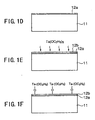
- a Si substrate 11 is held in a reaction vessel (not shown) under a reduced pressure environment of 133 - 399 Pa (1 - 3 Torr) at a temperature lower than a room temperature, and an oxide film 11a on the surface of the substrate 11 is removed by supplying nitrogen radicals N* and hydrogen radicals H* formed as a result of plasma activation of a gas mixture of N 2 and H 2 into the reaction vessel together with a NF 3 gas.
- a protective film 11b having a composition of N-O-Si-H on the surface of the Si substrate 11.
- the H 2 gas, the NF 3 gas and the N 2 gas are supplied with respective flow rates of 10 sccm, 30 sccm and 100 sccm, and the activation of the H 2 gas and the N 2 gas is achieved by applying a plasma power of about 50W.
- the process of FIG.1A may be continued for a duration of 3 minutes or less.
- the protective film 11b thus formed is a volatile film and easily undergoes vaporization by causing sublimation in the step of FIG.1C when the Si substrate 11 is annealed subsequently to the step of FIG.1B in the same reaction vessel under the reduced pressure environment at a temperature of about 120° C. As a result a fresh surface 11c of the Si substrate 11 is exposed.
- the pressure inside the reaction vessel is set to 1.33 - 13.3 Pa (0.01 - 0.1 Torr) and the substrate temperature is set to 200 - 350 °C.
- a SiCl 4 gas is introduced into the reaction vessel with a flow rate of 0.1 - 5 mg/min together with a He carrier gas, which is supplied to the reaction vessel with a flow rate of about 50 sccm.
- SiCl 4 molecules thus introduced with the SiCl 4 gas cause adsorption on the foregoing fresh surface 11c of the Si substrate 11.
- an H 2 O vapor is then introduced into the reaction vessel with a flow rate of about 1 sccm together with the He carrier gas, wherein the H 2 O vapor thus introduced causes a hydrolysis reaction in the SiCl 4 molecules absorbed on the surface 11c of the Si substrate 11.
- the SiO 2 molecular layer 12a containing one to several layers of SiO 2 molecules on the surface of the Si substrate 11.
- the SiO 2 molecular layer 12a may be replaced by a SiN molecular layer by processing the adsorbed SiCl 4 molecules by a NH 3 gas. Further, it is possible to form an SiON molecular layer by stacking the SiO 2 molecular layer and the SiN molecular layer as desired. Further, it is also possible to form a thermal oxide film in view of availability of abundant data for process control.
- the substrate temperature is set to 350°C or less, preferably about 300°C or less, most preferably to about 280°C, and a Ta(OC 2 H 5 ) 5 gas and an O 2 gas are supplied to the reaction vessel held at a pressure of 0.01 - 0.1 Torr similarly as before, together with a He carrier gas with respective flow rates of about 5 mg/min and 100 sccm for about 1 minute.
- the flow rate of the He carrier gas is set to about 100 sccm.
- the Ta(OC 2 H 5 ) 5 molecules are adsorbed on the SiO 2 layer 12a in the form of a Ta(OC 2 H 5 ) 5 molecular layer 12b.
- the substrate temperature is raised to about 350°C in an oxidizing atmosphere and oxidation or hydrolysis reaction is caused in the adsorbed Ta(OC 2 H 5 ) 5 molecules.
- the adsorbed molecular layer 12b of Ta(OC 2 H 5 )O 5 is converted into a Ta 2 O 5 molecular layer 12c.
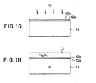
- the substrate temperature is raised to 510°C and the internal pressure of the reaction vessel is set to 13.3 - 1330 Pa (0.1 - 10 Torr).
- the Ta(OC 2 H 5 ) gas and the O 2 gas are introduced into the reaction vessel together with the He carrier gas and a Ta 2 O 5 film 13 is formed on the Ta 2 O 5 molecular layer 12c by an ordinary CVD process with a thickness of 4 - 5 nm.
- the Ta 2 O 5 film 13 is subjected to a thermal annealing process conducted in an O 2 atmosphere for compensation of oxygen defects and crystallization.
- the Ta 2 O 5 film 13 thus crystallized shows a large specific dielectric constant.
- the SiO 2 molecular layer 12a is interposed at the interface between the Si substrate 11 and the Ta 2 O 5 film 13
- a large carrier mobility is guaranteed for the semiconductor device formed on the Si substrate.
- the semiconductor device formed according to the present invention operates at a very high speed.
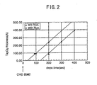
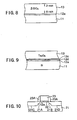
- FIG.2 shows the relationship between the duration of the deposition process in the CVD step of FIG.1H and the thickness of the Ta 2 O 5 film 13 thus formed, in comparison with a conventional CVD process of a Ta 2 O 5 films.
- the deposition time is measured from the point of commencement of the CVD process
- FIG.2 represents the deposition of the Ta 2 O 5 film according to the present embodiment
- ⁇ represents the deposition of the Ta 2 O 5 film according to the conventional CVD process.
- the CVD deposition of the Ta 2 O 5 film is conducted directly on the SiO 2 molecular layer 12a.
- the present invention can substantially reduce the incubation time at the time of forming a Ta 2 O 5 film by a CVD process.
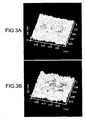
- FIGS.3A and 3B show the result of an AFM (atomic-force microscope) observation of the surface of the Ta 2 O 5 film formed on a SiON film covering the surface of the Si substrate by a conventional CVD process, wherein FIG.3A represents the case in which the CVD process of the Ta 2 O 5 film is conducted at the substrate temperature of 510°C, while FIG.3B represents the case in which the CVD process of the Ta 2 O 5 film is conducted at the substrate temperature of 480°C.
- AFM atomic-force microscope
- the CVD-Ta 2 O 5 film thus formed has a very large variation of film thickness reflecting the variation of the film thickness of the underlying SiON film.
- FIG.4A shows the surface of the Ta 2 O 5 film formed according to the present embodiment explained with reference to FIGS.1A - 1H , wherein it should be noted that the Ta 2 O 5 film is formed not on the SiO 2 molecular layer 12a but on an SiON molecular layer.
- FIG.4B shows the surface of the Ta 2 O 5 film deposited directly on the exposed surface 11c of the Si substrate 11. In any of FIGS.4A and 4B , the surface structure of the Ta 2 O 5 film was observed by an AFM.
- FIG.4A it can be seen that the projections and depressions on the Ta 2 O 5 film formed by the CVD process is reduced substantially by employing the process of the present invention.
- FIG.4A indicates that it is possible to obtain a Ta 2 O 5 film having a surface similar to that of the film formed directly on a Si substrate by employing the process of the present invention.
- this advantageous result of FIG.4A reflects the decrease of the incubation time achieved as a result of conducting the CVD process of the Ta 2 O 5 film 13 on the Ta 2 O 5 molecular layer 12c, which in turn is formed as a result of oxidation of the gaseous molecular compound Ta(OC 2 H 5 ) 5 adsorbed on the underlying SiON film layer, as explained with reference to FIG.2 .
- the variation of the incubation time itself is reduced, and the variation of the thickness of the Ta 2 O 5 film 13 thus formed by the CVD process is also reduced.
- the gaseous molecular compound usable for forming the Ta 2 O 5 molecular layer 12c is not limited to Ta(OC 2 H 5 ) 5 but it is also possible to use TaCl 5 .
- the adsorption process may be conducted by setting the internal pressure of the reaction vessel to 0.133 - 13.3 Pa (0.001 - 00.1 Torr) and by supplying the TaCl 5 gas with a flow rate of 0.1 - 5 mg/min while maintaining the substrate temperature of 200 - 300°C.
- the present invention is not limited to the process of forming a Ta 2 O 5 film but may be applicable also for forming various oxide films including a SiO 2 film, a ZrO 2 film, a HfO 2 film or an Al 2 O 3 film as summarized in FIGS.5 and 6 , wherein it should be noted that FIG.5 summarizes the process condition for the adsorption process and oxidizing process corresponding respectively to the steps of FIGS.1F and 1G ; for the foregoing oxides, while FIG.6 summarizes the process condition for the CVD process corresponding to the step of FIG.1H .
- the atmosphere used for oxidizing or causing hydrolysis reaction in the step of FIG.1F for forming the Ta 2 O 5 molecular layer 12c from the adsorbed Ta(OC 2 H 5 ) 5 molecules or TaCl 2 molecules is not limited to the O 2 atmosphere, but other oxidizing atmospheres including a H 2 O atmosphere, a NO 2 atmosphere or an O 3 atmosphere may also be used.
- the oxidizing atmosphere of FIG.1G is conducted in the O 2 atmosphere as explained before, it is preferable to set the internal pressure of the reaction vessel to 0.133 - 1330 Pa (0.01 - 10 Torr) and the substrate temperature of 300 - 400°C.
- the oxidizing step of FIG.1F is to be conducted in the 03 atmosphere, on the other hand, it is preferable to set the internal pressure of the reaction vessel to 0.133 - 1330 Pa (0.001 - 10 Torr) and the substrate temperature to 200 - 300°C.
- a ZrO 2 molecular layer in place of the Ta 2 O 5 molecular layer 12c by adsorbing a gaseous molecular compound of Zr such as Zr(t-OC 4 H 9 ) 4 or ZrCl 4 on the SiO 2 molecular layer 12a in the step of FIG.1F and oxidizing the same under a similar condition as in the case of using the Ta gaseous molecular compound in the step of FIG.1F .
- a gaseous molecular compound of Zr such as Zr(t-OC 4 H 9 ) 4 or ZrCl 4
- HfO 2 molecular layer by adsorbing a gaseous molecular compound of Hf such as Hf(t-OC 4 H 9 ) 4 or HfCl 4 on the SiO 2 molecular layer 12a and oxidizing the same under a similar condition as in the case of forming the Ta 2 O 5 molecular layer.
- a gaseous molecular compound of Hf such as Hf(t-OC 4 H 9 ) 4 or HfCl 4
- an Al 2 O 3 molecular layer in place of the Ta 2 O 5 molecular layer 12c by adsorbing a gaseous molecular compound of Al such as Al(1-OC 3 H 7 ) 3 or (CH 3 ) 3 Al on the SiO 2 molecular layer 12a and oxidizing the same under a similar condition as in the case of forming the Ta 2 O 5 molecular layer.
- a gaseous molecular compound of Al such as Al(1-OC 3 H 7 ) 3 or (CH 3 ) 3 Al
- the molecular layer 12c from SiO 2 by adsorbing Si(OC 2 H 5 ) 4 or SiCl 4 or SiH 2 Cl 2 on the SiO 2 molecular layer 12a under the condition similar to that of the Ta 2 O 5 molecular layer and further causing oxidation or hydrolysis in the gaseous molecular compound of Si thus absorbed under a similar condition.
- FIG.7 shows the process of forming a dielectric film according to a second embodiment of the present invention in the form of flowchart.
- the gaseous molecules of SiCl 4 are adsorbed on the SiO 2 molecular layer 12a represented in FIG.1D in the step S1, and the SiCl 4 molecules thus adsorbed are subjected to an oxidation or hydrolysis reaction in the step S2. As a result, there is formed a molecular layer of SiO 2 on the substrate 11.
- steps S1 and S2 are repeated alternately a predetermined times X in the next step S3, and the process proceeds further to the step S4 corresponding to the process steps of FIGS.1E and 1F in which the molecules of ZrCl 4 or Zr(t-OC 4 H 9 ) 4 are adsorbed on the SiO 2 molecular layer formed in the previous steps S1 and S2.
- the gaseous molecular compound of Zr thus adsorbed are then subjected to an oxidation or hydrolysis reaction in the next step S5 corresponding to the process step of FIG.1G , and there is formed a molecular layer of ZrO 2 on the SiO 2 molecular layer. Further, the foregoing steps S4 and S5 are repeated alternately Y times in the next step S6, and the number of repetition X and Y are changed to X1 and Y1 respectively in the next step S7.
- the process returns to the step S1.
- a dielectric film having a composition of ZrSi04 on the Si substrate in such a manner that the proportion of Zr and Si changes continuously in the thickness direction of the layer as represented in FIG.8 , wherein FIG.8 represents those parts corresponding to the parts described previously by corresponding reference numerals.
- the Zr content in the dielectric film is controlled such that the Zr content is small in the vicinity of the interface to the Si substrate 11 and increases with increasing distance from the foregoing interface.
- the ZrSiO 4 film having such a compositional profile there is an advantageous feature, associated with the increased Si content in the vicinity of the interface to the Si substrate, of improved adherence.
- the leakage current through the dielectric film is suppressed effectively.
- FIG.9 shows the structure of a dielectric film according to a third embodiment of the present invention, wherein those parts corresponding to the parts described previously are designated by the same reference numerals and the description thereof will be omitted.
- the present embodiment carries out adsorption of SiCl 4 molecules on the SiO 2 molecular layer 12a and the SiCl 4 molecules are converted to a molecular layer 12d of SiN by processing the adsorbed SiCl 4 molecules by an NH 3 gas.
- the Ta(OC 2 H 5 ) 5 molecules are adsorbed on the layer 12d, and are converted to the Ta 2 O 5 molecular layer 12c as a result of oxidation.
- the CVD-Ta 2 O 5 layer 13 is formed on the Ta 2 O 5 molecular layer 12c.
- the structure of FIG.9 it is possible to eliminate the problem of diffusion of B into the Si substrate by the SiN molecular layer 12d when a B-doped polysilicon film is deposited on the Ta 2 O 5 film 13. It should be noted that the SiN molecular layer 12d interposed between the Ta 2 O 5 film 13 and the Si substrate 11 effectively blocks the diffusion of B. Thus, the structure of FIG.9 is effective for eliminating the variation of the threshold characteristic
- FIG.10 shows the construction of a semiconductor device according to a fourth embodiment of the present invention.
- a gate insulation film 22 of Ta 2 O 5 on a p-type substrate according to a process described in any of the preceding embodiments, and a polysilicon gate electrode 23 is formed on the gate insulation film 22.
- the Si substrate 21 is formed with diffusion regions 21A and 21B of n - -type adjacent to the gate electrode 23, and sidewall insulation films 23a and 23b are provided on respective sidewalls of the polysilicon gate electrode 23. Further, diffusion regions 21C and 21D of n + -type are formed outside of the sidewall insulation films 23a and 23b respectively.
- an effective film thickness electrically equivalent to a SiO2 film having a thickness of 0.1 nm or less is realized by using Ta 2 O 5 for the gate insulation film 22, and a ultrahigh-speed operation is achieved by reducing the gate length while simultaneously suppressing the gate leakage current.
- Ta 2 O 5 film 22 By forming the Ta 2 O 5 film 22 according to the process described in any of the preceding embodiments, it becomes possible to minimize the variation of the film thickness and the semiconductor device thus formed has reliable and reproducible characteristics. Particularly, it is possible to block the diffusion of the impurity element from the gate electrode 12 to the Si substrate 21 by intervening a molecular layer 12d of SiN right underneath the Ta 2 O 5 film 22 with a thickness of several molecular layers.
- the gate insulation film 22 By forming the gate insulation film 22 in the form of stacking of molecular layers of various oxides including Ta205, it is possible to control the compositional profile inside the gate insulation film 22 in the thickness direction thereof as desired. As a result, a structure having excellent adhesion to the Si substrate can be formed easily for the gate insulation film, such that the gate insulation film has a large specific dielectric constant at the interface to the gate electrode 23.
- the present invention it becomes possible to form a dielectric or high-dielectric film of various compositions including Ta 2 O 5 on a Si substrate by a CVD process with reduced incubation time. As a result, the uniformity of the obtained dielectric film is improved. Further, the present invention enables control of composition of the dielectric film in the thickness direction thereof. According to the needs, it is also possible to form an extremely thin diffusion barrier film of about a single molecular layer thickness in the dielectric film. In view of the fact that the present invention does not include the step of using plasma-excited radials, the dielectric film thus formed according to the process of the present invention is substantially free form defects having electric charges such as impurity states, and excellent leakage characteristics can be attained. As a result of the present invention, a ultrafine and ultrahigh-speed semiconductor device having a gate length of 0.1 ⁇ m or less can be formed while successfully suppressing the gate leakage current.
Abstract
Description
- The present invention generally relates to semiconductor devices and more particularly to a fabrication process of ultrafine and ultrahigh-speed semiconductor devices.
- With advancement in the art of device miniaturization, it is now becoming possible to use a gate length of 0.1 µm or less in leading-edge, ultrahigh-speed semiconductor devices. With increase in the degree of device miniaturization, it is well known that there occurs an increase of the operational speed. On the other hand, in order to achieve such an increase of operational speed by way of device miniaturization, there is a requirement, from scaling law, to reduce the thickness of a gate insulation film used therein in proportion with the reduction of a gate length of the semiconductor device.
- In the case of ultrafine and ultrahigh-speed semiconductor devices having the gate length of 0.1 µm or less, it is thus necessary to reduce the thickness of the gate electrode to 1 - 2 nm or less, provided that SiO2 is used for the material of the gate insulation film. However, the use of such an extremely thin gate insulation film inevitably causes the problem of increase of leakage current caused by the tunneling effect through the thin gate insulation film.
- Thus, in order to avoid the foregoing problem associated with the use of the SiO2 film, there is proposed in Japanese Laid-Open Patent Publication
11-87341 - This prior art process, however, is not effective for eliminating the foregoing problem of tunneling leakage current. Although SiN has a specific dielectric constant of about 8, which is certainly larger than the specific constant of 4 for SiO2. this value is not sufficient for achieving the desired increase of the physical thickness of the gate insulation film while eliminating the tunneling current.
- The process of the foregoing prior art has a further drawback, in relation to the use of the nitrogen radicals, in that it requires a plasma process for exciting the nitrogen radicals. When the substrate surface is processed in the vicinity of a plasma source, charged particles forming the plasma such as electrons or ions are incorporated into the SiN film and form impurity states therein. When such impurity states are formed in the gate insulation film, the leakage current in the gate insulation film is increased and the CV characteristic is degraded. When the plasma source is provided at a remote location away from the substrate so as to avoid the foregoing problem, on the other hand, the number of the nitrogen radicals is reduced at the surface of the substrate and the adsorption of nitrogen becomes difficult.
- In view of the situation noted above, there is a proposal to use a high-dielectric material such as Ta2O5 for the material of the gate insulation film. It should be noted that these high-dielectric materials have a far larger specific dielectric constant as compared with SiO2. By using such a high-dielectric material, it becomes possible to effectively reduce the equivalent thickness of the insulation film, which is an electrically equivalent thickness converted to the thickness of a SiO2 film, while simultaneously using a large physical thickness. By using such a high-dielectric gate insulation film, it becomes possible to use a physical thickness of about 10 nm for the gate insulation film of ultrafine and ultrahigh-speed semiconductor devices having a gate length of 0.1 µm or less, while successfully suppressing the gate leakage current caused by tunneling effect.
- It has been known that a Ta2O5 film can be formed by a CVD process that uses Ta(OC2H5)2 and O2 as gaseous source. In a typical example, the CVD process is conducted under a reduced pressure environment at a temperature of 480° C or more. The Ta2O5 film thus formed is then annealed in an oxidizing atmosphere for compensating for oxygen defects and for crystallization of the film. The Ta2O5 film thus crystallized shows a very large specific dielectric constant.
- When growing a high-dielectric film such as Ta2O5 on a Si substrate by a CVD process, it is known that the growth of the high-dielectric film does not start immediately after the commencement of the CVD process due to a delay caused by nucleation process and that the growth starts only after a certain incubation time has elapsed.
- In the experimental investigation that constitutes the foundation of the present invention, the inventor of the present invention has discovered that the incubation time varies depending on the nature of the layer on which the high-dielectric film is deposited. For example, the incubation time becomes very short when the deposition is made on a clean surface of a Si substrate from which oxide is removed. When there is an insulating film of SiO2 or a SiN or SiON on a Si substrate, on the other hand, a remarkable increase of the incubation time was observed. Further, it was discovered that the incubation time changes also depending on the thickness of the SiO2 film or SiN film or the SiON film existing on the surface of the Si substrate.
- The foregoing discovery means that the thickness of the high-dielectric film formed on a SiO2 film or on a SiN film or on a SiON film on a Si substrate tends to reflect the variation of thickness of the underlying layer and that there may be a case in which the variation of the thickness of the underlying layer may be amplified by the high-dielectric film. Further, the observed fact that the thickness of the high-dielectric film thus formed by a CVD process is affected by the nature of the underlying layer indicates that the quality of the high-dielectric film thus formed for the gate insulation film may lack the desired homogeneity.
- In order to suppress the occurrence of inhomogeneity in such high-dielectric film, it is necessary as well as desired to reduce the incubation time as much as possible.
- Meanwhile, in such a semiconductor device that uses a high-dielectric film for the gate insulation film, it is necessary as well as desired to provide a thin oxide film between the Si substrate and the high-dielectric gate insulation film for eliminating the diffusion of metal elements or impurity elements into the substrate forming the channel region of the semiconductor device from or through the high-dielectric film. Otherwise, there may be caused a problem of carrier scattering in the channel region by the metal elements.
- On the other hand, such an intervening oxide film has to be extremely thin. When a thick oxide film is interposed between the Si substrate and the high-dielectric film, the effect of the high-dielectric film would be canceled out. In addition, there is a demand for a technology to change a film quality such as composition in the thickness direction of the high-dielectric film.
- Accordingly, it is a general object of the present invention to provide a novel and useful method of forming a dielectric film wherein the foregoing problems are eliminated.
- Another and more specific object of the present invention is to provide a method of forming a dielectric film by a vapor phase deposition process without causing damages in the dielectric film by charged particles while minimizing the incubation time for deposition of the dielectric film and simultaneously reducing the surface roughness.
- Another object of the present invention is to provide a method of forming a dielectric film by a vapor phase deposition process without causing damages in the dielectric film by charged particles while arbitrarily controlling a compositional profile of the dielectric film in a thickness direction thereof .
- These objects of the present invention are solved by the method of claim 1.
- According to the present invention, it becomes possible to form a dielectric or high-dielectric film of various compositions including Ta2O5 on a Si substrate by a CVD process with reduced incubation time. As a result, the uniformity of the obtained dielectric film is improved. Further, the present invention enables control of the composition of the dielectric film in the thickness direction thereof. According to the needs, it is also possible to form an extremely thin diffusion barrier film of about a single molecular layer thickness inside the dielectric film. In view of the fact that the present invention does not include the step of using plasma-excited radicals, the dielectric film thus formed according to the process of the present invention is substantially free from defects having electric charges such as impurity states, and excellent leakage characteristics can be attained.
- As a result of the present invention, a ultrafine and ultrahigh-speed semiconductor device having a gate length of 0.1 µm or less can be formed while successfully suppressing the gate leakage current.
- Other objects and further features of the present invention will become apparent from the following detailed description when read in conjunction with the attached drawings.
-
-
FIGS.1A - 1H are diagrams showing the process of forming a dielectric film according to a first embodiment of the present invention; -
FIG.2 is a diagram showing the effect of the present invention; -
FIGS.3A and 3B are diagrams showing a surface structure of a Ta2O5 film formed on a SiON film according to a conventional CVD process; -
FIGS.4A and 4B are diagrams respectively showing the surface structure of a Ta2O5 film formed on a SiON substrate according to a process of the present invention and the surface structure of a Ta2O5 film formed directly on a Si substrate surface; -
FIG.5 is a diagram showing the process conditions used in the present embodiment and in various modifications thereof; -
FIG.6 is a further diagram showing the process conditions used in the present embodiment and in various modifications thereof; -
FIG.7 is a flowchart showing the process of forming a dielectric film according to a second embodiment of the present invention; -
FIG.8 is a diagram showing the structure of a dielectric film formed according to the second embodiment of the present invention; -
FIG.9 is a diagram showing the structure of a dielectric film formed according to a third embodiment of the present invention; and -
FIG.10 is a diagram showing the construction of a semiconductor device according to a fourth embodiment of the present invention. -
FIGS.1A - 1H show the process of forming a Ta2O5 film according to a first embodiment of the present invention. - Referring to
FIG.1A , aSi substrate 11 is held in a reaction vessel (not shown) under a reduced pressure environment of 133 - 399 Pa (1 - 3 Torr) at a temperature lower than a room temperature, and anoxide film 11a on the surface of thesubstrate 11 is removed by supplying nitrogen radicals N* and hydrogen radicals H* formed as a result of plasma activation of a gas mixture of N2 and H2 into the reaction vessel together with a NF3 gas. By conducting such a removal of the oxide film at low temperature, there is formed aprotective film 11b having a composition of N-O-Si-H on the surface of theSi substrate 11. In a typical example, the H2 gas, the NF3 gas and the N2 gas are supplied with respective flow rates of 10 sccm, 30 sccm and 100 sccm, and the activation of the H2 gas and the N2 gas is achieved by applying a plasma power of about 50W. The process ofFIG.1A may be continued for a duration of 3 minutes or less. - The
protective film 11b thus formed is a volatile film and easily undergoes vaporization by causing sublimation in the step ofFIG.1C when theSi substrate 11 is annealed subsequently to the step ofFIG.1B in the same reaction vessel under the reduced pressure environment at a temperature of about 120° C. As a result afresh surface 11c of theSi substrate 11 is exposed. - Next, in the step of
FIG.1D , which is continued from the step ofFIG.1C , the pressure inside the reaction vessel is set to 1.33 - 13.3 Pa (0.01 - 0.1 Torr) and the substrate temperature is set to 200 - 350 °C. In this state, a SiCl4 gas is introduced into the reaction vessel with a flow rate of 0.1 - 5 mg/min together with a He carrier gas, which is supplied to the reaction vessel with a flow rate of about 50 sccm. In this step, SiCl4 molecules thus introduced with the SiCl4 gas cause adsorption on the foregoingfresh surface 11c of theSi substrate 11. - In the step of
FIG.1D , an H2O vapor is then introduced into the reaction vessel with a flow rate of about 1 sccm together with the He carrier gas, wherein the H2O vapor thus introduced causes a hydrolysis reaction in the SiCl4 molecules absorbed on thesurface 11c of theSi substrate 11. As a result, there is formed an extremely thin SiO2molecular layer 12a containing one to several layers of SiO2 molecules on the surface of theSi substrate 11. By repeating the process of introducing the SiCl4 gas and the process of hydrolysis of the absorbed SiCl4 molecules in the step ofFIG.1D , it is possible to form the SiO2molecular layer 12a to have a desired thickness. - In the step of
FIG.1D , it is also possible to use a SiH2Cl2 gas or a Si(C2H5)5 gas in place of the SiCl4 gas. - In the step of
FIG.1D , it should also be noted that the SiO2molecular layer 12a may be replaced by a SiN molecular layer by processing the adsorbed SiCl4 molecules by a NH3 gas. Further, it is possible to form an SiON molecular layer by stacking the SiO2 molecular layer and the SiN molecular layer as desired. Further, it is also possible to form a thermal oxide film in view of availability of abundant data for process control. - Next, in the step of
FIG.1E , the substrate temperature is set to 350°C or less, preferably about 300°C or less, most preferably to about 280°C, and a Ta(OC2H5)5 gas and an O2 gas are supplied to the reaction vessel held at a pressure of 0.01 - 0.1 Torr similarly as before, together with a He carrier gas with respective flow rates of about 5 mg/min and 100 sccm for about 1 minute. The flow rate of the He carrier gas is set to about 100 sccm. As a result, the Ta(OC2H5)5 molecules are adsorbed on the SiO2 layer 12a in the form of a Ta(OC2H5)5molecular layer 12b. - Next, in the step of
FIG.1G , the substrate temperature is raised to about 350°C in an oxidizing atmosphere and oxidation or hydrolysis reaction is caused in the adsorbed Ta(OC2H5)5 molecules. As a result, the adsorbedmolecular layer 12b of Ta(OC2H5)O5 is converted into a Ta2O5molecular layer 12c. - Further, in the step of
FIG.1H , the substrate temperature is raised to 510°C and the internal pressure of the reaction vessel is set to 13.3 - 1330 Pa (0.1 - 10 Torr). Further, the Ta(OC2H5) gas and the O2 gas are introduced into the reaction vessel together with the He carrier gas and a Ta2O5 film 13 is formed on the Ta2O5molecular layer 12c by an ordinary CVD process with a thickness of 4 - 5 nm. - While not illustrated, the Ta2O5 film 13 is subjected to a thermal annealing process conducted in an O2 atmosphere for compensation of oxygen defects and crystallization. The Ta2O5 film 13 thus crystallized shows a large specific dielectric constant. In view of the fact that the SiO2
molecular layer 12a is interposed at the interface between theSi substrate 11 and the Ta2O5 film 13, a large carrier mobility is guaranteed for the semiconductor device formed on the Si substrate. In other words, the semiconductor device formed according to the present invention operates at a very high speed. -
FIG.2 shows the relationship between the duration of the deposition process in the CVD step ofFIG.1H and the thickness of the Ta2O5 film 13 thus formed, in comparison with a conventional CVD process of a Ta2O5 films. InFIG.2 , it should be noted that the deposition time is measured from the point of commencement of the CVD process InFIG.2 , represents the deposition of the Ta2O5 film according to the present embodiment, while ▲ represents the deposition of the Ta2O5 film according to the conventional CVD process. In the conventional experiments represented by ▲, it should be noted that the CVD deposition of the Ta2O5 film is conducted directly on the SiO2molecular layer 12a. - Referring to
FIG.2 , it can be seen that there exists an incubation time of about 140 seconds from the start of the CVD process until actual deposition of the Ta2O5 film is caused, while in the case of the present invention, the deposition of the Ta2O5 film is already started after 40 seconds from the commencement of the CVD process. Thus, the present invention can substantially reduce the incubation time at the time of forming a Ta2O5 film by a CVD process. -
FIGS.3A and 3B show the result of an AFM (atomic-force microscope) observation of the surface of the Ta2O5 film formed on a SiON film covering the surface of the Si substrate by a conventional CVD process, whereinFIG.3A represents the case in which the CVD process of the Ta2O5 film is conducted at the substrate temperature of 510°C, whileFIG.3B represents the case in which the CVD process of the Ta2O5 film is conducted at the substrate temperature of 480°C. - Referring to
FIGS.3A and 3B , the CVD-Ta2O5 film thus formed has a very large variation of film thickness reflecting the variation of the film thickness of the underlying SiON film. In other words, there occurs an amplification of thickness variation of the underlying layer in the conventional CVD-Ta2O5 film and the homogeneity of the obtained Ta2O5 film becomes inevitably deteriorated. -
FIG.4A , on the other hand, shows the surface of the Ta2O5 film formed according to the present embodiment explained with reference toFIGS.1A - 1H , wherein it should be noted that the Ta2O5 film is formed not on the SiO2molecular layer 12a but on an SiON molecular layer.FIG.4B , on the other hand, shows the surface of the Ta2O5 film deposited directly on the exposedsurface 11c of theSi substrate 11. In any ofFIGS.4A and 4B , the surface structure of the Ta2O5 film was observed by an AFM. - Referring to
FIG.4A , it can be seen that the projections and depressions on the Ta2O5 film formed by the CVD process is reduced substantially by employing the process of the present invention. In other words,FIG.4A indicates that it is possible to obtain a Ta2O5 film having a surface similar to that of the film formed directly on a Si substrate by employing the process of the present invention. It is believed that this advantageous result ofFIG.4A reflects the decrease of the incubation time achieved as a result of conducting the CVD process of the Ta2O5 film 13 on the Ta2O5molecular layer 12c, which in turn is formed as a result of oxidation of the gaseous molecular compound Ta(OC2H5)5 adsorbed on the underlying SiON film layer, as explained with reference toFIG.2 . As a result of the decrease of the incubation time depending on the quality of the underlying film, the variation of the incubation time itself is reduced, and the variation of the thickness of the Ta2O5 film 13 thus formed by the CVD process is also reduced. - In the present invention, it should be noted that the gaseous molecular compound usable for forming the Ta2O5
molecular layer 12c is not limited to Ta(OC2H5)5 but it is also possible to use TaCl5. When TaCl5 is used, the adsorption process may be conducted by setting the internal pressure of the reaction vessel to 0.133 - 13.3 Pa (0.001 - 00.1 Torr) and by supplying the TaCl5 gas with a flow rate of 0.1 - 5 mg/min while maintaining the substrate temperature of 200 - 300°C. - Further, the present invention is not limited to the process of forming a Ta2O5 film but may be applicable also for forming various oxide films including a SiO2 film, a ZrO2 film, a HfO2 film or an Al2O3 film as summarized in
FIGS.5 and6 , wherein it should be noted thatFIG.5 summarizes the process condition for the adsorption process and oxidizing process corresponding respectively to the steps ofFIGS.1F and1G ; for the foregoing oxides, whileFIG.6 summarizes the process condition for the CVD process corresponding to the step ofFIG.1H . - Referring to
FIG.5 , it can be seen that the atmosphere used for oxidizing or causing hydrolysis reaction in the step ofFIG.1F for forming the Ta2O5molecular layer 12c from the adsorbed Ta(OC2H5)5 molecules or TaCl2 molecules is not limited to the O2 atmosphere, but other oxidizing atmospheres including a H2O atmosphere, a NO2 atmosphere or an O3 atmosphere may also be used. In the event the oxidizing atmosphere ofFIG.1G is conducted in the O2 atmosphere as explained before, it is preferable to set the internal pressure of the reaction vessel to 0.133 - 1330 Pa (0.01 - 10 Torr) and the substrate temperature of 300 - 400°C. In the event the oxidizing step ofFIG.1F is to be conducted in the 03 atmosphere, on the other hand, it is preferable to set the internal pressure of the reaction vessel to 0.133 - 1330 Pa (0.001 - 10 Torr) and the substrate temperature to 200 - 300°C. - As can be seen in
FIG.5 , it is also possible to form a ZrO2 molecular layer in place of the Ta2O5molecular layer 12c by adsorbing a gaseous molecular compound of Zr such as Zr(t-OC4H9)4 or ZrCl4 on the SiO2molecular layer 12a in the step ofFIG.1F and oxidizing the same under a similar condition as in the case of using the Ta gaseous molecular compound in the step ofFIG.1F . Similarly, it is also possible to form a HfO2 molecular layer by adsorbing a gaseous molecular compound of Hf such as Hf(t-OC4H9)4 or HfCl4 on the SiO2molecular layer 12a and oxidizing the same under a similar condition as in the case of forming the Ta2O5 molecular layer. Further, it is possible to form an Al2O3 molecular layer in place of the Ta2O5molecular layer 12c by adsorbing a gaseous molecular compound of Al such as Al(1-OC3H7)3 or (CH3)3Al on the SiO2molecular layer 12a and oxidizing the same under a similar condition as in the case of forming the Ta2O5 molecular layer. - It is also possible to form the
molecular layer 12c from SiO2 by adsorbing Si(OC2H5)4 or SiCl4 or SiH2Cl2 on the SiO2molecular layer 12a under the condition similar to that of the Ta2O5 molecular layer and further causing oxidation or hydrolysis in the gaseous molecular compound of Si thus absorbed under a similar condition. - Further, by conducting a CVD process on the oxide
molecular layer 12c thus formed under the condition summarized inFIG.6 , it becomes possible to form a CVD film of various oxides including Ta2O5, ZrO2, HfO2, SiO2 and Al2O3 as theCVD film 13. -
FIG.7 shows the process of forming a dielectric film according to a second embodiment of the present invention in the form of flowchart. - Referring to
FIG.7 , the gaseous molecules of SiCl4 are adsorbed on the SiO2molecular layer 12a represented inFIG.1D in the step S1, and the SiCl4 molecules thus adsorbed are subjected to an oxidation or hydrolysis reaction in the step S2. As a result, there is formed a molecular layer of SiO2 on thesubstrate 11. - The foregoing steps S1 and S2 are repeated alternately a predetermined times X in the next step S3, and the process proceeds further to the step S4 corresponding to the process steps of
FIGS.1E and 1F in which the molecules of ZrCl4 or Zr(t-OC4H9)4 are adsorbed on the SiO2 molecular layer formed in the previous steps S1 and S2. - The gaseous molecular compound of Zr thus adsorbed are then subjected to an oxidation or hydrolysis reaction in the next step S5 corresponding to the process step of
FIG.1G , and there is formed a molecular layer of ZrO2 on the SiO2 molecular layer. Further, the foregoing steps S4 and S5 are repeated alternately Y times in the next step S6, and the number of repetition X and Y are changed to X1 and Y1 respectively in the next step S7. - After the step S7, the process returns to the step S1. Thus, by repeating the steps S1 - S7 with the newly defined number of the repetition X1 and Y1, there is formed a dielectric film having a composition of ZrSi04 on the Si substrate in such a manner that the proportion of Zr and Si changes continuously in the thickness direction of the layer as represented in
FIG.8 , whereinFIG.8 represents those parts corresponding to the parts described previously by corresponding reference numerals. - Referring to
FIG.8 , it can be seen that the Zr content in the dielectric film is controlled such that the Zr content is small in the vicinity of the interface to theSi substrate 11 and increases with increasing distance from the foregoing interface. In the ZrSiO4 film having such a compositional profile, there is an advantageous feature, associated with the increased Si content in the vicinity of the interface to the Si substrate, of improved adherence. Further, in view of the fact that the large Zr content in the vicinity of the surface of the ZrSiO4 film, the leakage current through the dielectric film is suppressed effectively. Further, it is possible to form the ZrSiO4 film such that a Zr atom and a Si atom are repeated alternately in the thickness direction in every one molecular layer in the ZrSiO4 film. -
FIG.9 shows the structure of a dielectric film according to a third embodiment of the present invention, wherein those parts corresponding to the parts described previously are designated by the same reference numerals and the description thereof will be omitted. - Referring to
FIG.9 , the present embodiment carries out adsorption of SiCl4 molecules on the SiO2molecular layer 12a and the SiCl4 molecules are converted to amolecular layer 12d of SiN by processing the adsorbed SiCl4 molecules by an NH3 gas. After the formation of the SiNmolecular layer 12d, the Ta(OC2H5)5 molecules are adsorbed on thelayer 12d, and are converted to the Ta2O5molecular layer 12c as a result of oxidation. Further, the CVD-Ta2O5 layer 13 is formed on the Ta2O5molecular layer 12c. - In the structure of
FIG.9 , it is possible to eliminate the problem of diffusion of B into the Si substrate by the SiNmolecular layer 12d when a B-doped polysilicon film is deposited on the Ta2O5 film 13. It should be noted that the SiNmolecular layer 12d interposed between the Ta2O5 film 13 and theSi substrate 11 effectively blocks the diffusion of B. Thus, the structure ofFIG.9 is effective for eliminating the variation of the threshold characteristic -
FIG.10 shows the construction of a semiconductor device according to a fourth embodiment of the present invention. - Referring to
FIG.10 , there is formed agate insulation film 22 of Ta2O5 on a p-type substrate according to a process described in any of the preceding embodiments, and apolysilicon gate electrode 23 is formed on thegate insulation film 22. - Further, the
Si substrate 21 is formed withdiffusion regions gate electrode 23, and sidewall insulation films 23a and 23b are provided on respective sidewalls of thepolysilicon gate electrode 23. Further,diffusion regions - In the semiconductor device of
FIG.10 , an effective film thickness electrically equivalent to a SiO2 film having a thickness of 0.1 nm or less is realized by using Ta2O5 for thegate insulation film 22, and a ultrahigh-speed operation is achieved by reducing the gate length while simultaneously suppressing the gate leakage current. By forming the Ta2O5 film 22 according to the process described in any of the preceding embodiments, it becomes possible to minimize the variation of the film thickness and the semiconductor device thus formed has reliable and reproducible characteristics. Particularly, it is possible to block the diffusion of the impurity element from the gate electrode 12 to theSi substrate 21 by intervening amolecular layer 12d of SiN right underneath the Ta2O5 film 22 with a thickness of several molecular layers. - By forming the
gate insulation film 22 in the form of stacking of molecular layers of various oxides including Ta205, it is possible to control the compositional profile inside thegate insulation film 22 in the thickness direction thereof as desired. As a result, a structure having excellent adhesion to the Si substrate can be formed easily for the gate insulation film, such that the gate insulation film has a large specific dielectric constant at the interface to thegate electrode 23. - As the forgoing process of forming the dielectric molecular film on the substrate is achieved by a hydrolysis reaction of the adsorbed gaseous source molecules in the present invention contrary to the conventional process of the Japanese Laid-Open Patent Publication
11-97341 - Further, the present invention is not limited to the embodiments described heretofore, but various variations and modifications may be made without departing from the scope of the invention.
- According to the present invention, it becomes possible to form a dielectric or high-dielectric film of various compositions including Ta2O5 on a Si substrate by a CVD process with reduced incubation time. As a result, the uniformity of the obtained dielectric film is improved. Further, the present invention enables control of composition of the dielectric film in the thickness direction thereof. According to the needs, it is also possible to form an extremely thin diffusion barrier film of about a single molecular layer thickness in the dielectric film. In view of the fact that the present invention does not include the step of using plasma-excited radials, the dielectric film thus formed according to the process of the present invention is substantially free form defects having electric charges such as impurity states, and excellent leakage characteristics can be attained. As a result of the present invention, a ultrafine and ultrahigh-speed semiconductor device having a gate length of 0.1 µm or less can be formed while successfully suppressing the gate leakage current.
Claims (11)
- A method of forming a metal oxide dielectric film on a Si substrate, comprising the steps of:exposing a surface of said Si substrate;forming an insulating layer on said exposed surface of said Si substrate; and forming the film of metal oxide on said insulating layer,wherein said step of forming said film of metal oxide comprises the steps of:causing adsorption of a gaseous molecular compound of a metal element constituting the metal oxide on a surface of said insulating layer, such that said gaseous molecular compound covers said insulating layer; andcausing hydrolysis or oxidation of said gaseous molecular compound covering said surface of said insulating layer, by exposing said gaseous molecular compound covering said surface of said insulating layer to an ambient of H2O or an oxidizing agent.
- The method as claimed in claim 1, wherein said oxidizing agent comprises any of O3 and NO2.
- The method as claimed in claim 1 or 2, wherein said metal oxide comprises Ta2O5 and wherein said gaseous molecular compound comprises one of Ta(OC2H5)5 and TaCl5.
- The method as claimed in claim 1 or 2, wherein said metal oxide comprises ZrO2 and wherein said gaseous molecular compound comprises one of Zr(t-OC4H9)4 and ZrCl4.
- The method as claimed in claim 1 or 2, wherein said metal oxide comprises HfO2 and wherein said gaseous molecular compound comprises one of Hf(t-OC4H9)4 and HfCl4.
- The method as claimed in claim 1 or 2, wherein said metal oxide comprises Al2O3 and wherein said gaseous molecular compound comprises one of Al(1-OC3H7)3 and (CH3)3Al.
- The method as claimed in any of claims 1 - 6, wherein said insulating layer comprises one of SiO2, SiN and SiON.
- The method as claimed in claim 7, wherein said insulating layer is SiO2 which is formed by the steps of: causing adsorption of a gaseous molecular compound of Si on said exposed surface of said Si substrate such that said gaseous molecular compound of Si covers said exposed surface of said Si substrate; and causing hydrolysis of said gaseous molecular compound of Si covering said Si substrate by exposing said gaseous compound of Si to an ambient of H2O, such that a molecular layer of SiO2 is formed, said gaseous molecular compound of Si being selected from the group consisting of SiCl4, SiH2Cl2 and Si(C2H5)5.
- The method as claimed in claim 7, wherein said insulating layer is SiN which is formed by the steps of: causing adsorption of a gaseous molecular compound of Si on said exposed surface of said Si substrate such that said gaseous molecular compound of Si covers said exposed surface of said Si substrate; and causing nitridation of said gaseous molecular compound of Si covering said Si substrate by exposing said gaseous compound of Si to an ambient of a NH3 gas, such that a molecular layer of SiN is formed, said gaseous molecular compound of Si being selected from the group consisting of SiCl4, SiH2Cl2 and Si(C2H5)5.
- The method as claimed in any of claims 1 - 9, further comprising, after said step of forming said film of said metal oxide, a step of forming a high-dielectric film on said film of said metal oxide by a CVD process.
- The method as claimed in any of claims 1 - 9, wherein said step of forming said dielectric film of metal oxide comprises the step of forming a dielectric film having a composition represented as ZrSiO4, such that said dielectric film has a low Zr concentration level at an interface to said Si substrate and such that said Zr concentration level increases with increasing distance from said interface, by repeating a step of forming a SiO2 molecular layer and then repeating a step of forming a ZiO2 molecular layer and finally repeating said cycle of SiO2 and ZiO2 formation, said step of forming said SiO2 molecular layer comprising the steps of: adsorbing molecules of a first gaseous source material containing Si on an underlying layer; and decomposing said adsorbed molecules of said first gaseous source material using hydrolysis or oxidation, said step of forming said ZiO2 molecular layer comprising the steps of: adsorbing molecules of a second gaseous source material containing a metal element on an underlying layer; and decomposing said adsorbed molecules of said second gaseous source material using hydrolysis or oxidation.
Applications Claiming Priority (3)
| Application Number | Priority Date | Filing Date | Title |
|---|---|---|---|
| JP2000095818 | 2000-03-30 | ||
| JP2000095818A JP4493796B2 (en) | 2000-03-30 | 2000-03-30 | Method for forming dielectric film |
| PCT/JP2001/002262 WO2001075956A1 (en) | 2000-03-30 | 2001-03-22 | Method of forming a dielectric film |
Publications (2)
| Publication Number | Publication Date |
|---|---|
| EP1269528A1 EP1269528A1 (en) | 2003-01-02 |
| EP1269528B1 true EP1269528B1 (en) | 2012-06-20 |
Family
ID=18610667
Family Applications (1)
| Application Number | Title | Priority Date | Filing Date |
|---|---|---|---|
| EP01915684A Expired - Lifetime EP1269528B1 (en) | 2000-03-30 | 2001-03-22 | Method of forming a dielectric film |
Country Status (6)
| Country | Link |
|---|---|
| US (1) | US6866890B2 (en) |
| EP (1) | EP1269528B1 (en) |
| JP (1) | JP4493796B2 (en) |
| KR (1) | KR100752559B1 (en) |
| TW (1) | TW486762B (en) |
| WO (1) | WO2001075956A1 (en) |
Families Citing this family (19)
| Publication number | Priority date | Publication date | Assignee | Title |
|---|---|---|---|---|
| JP4095326B2 (en) | 2002-03-29 | 2008-06-04 | 株式会社東芝 | Semiconductor device manufacturing method and semiconductor device |
| JP2004140292A (en) | 2002-10-21 | 2004-05-13 | Tokyo Electron Ltd | Forming method of dielectric film |
| JP2005093909A (en) * | 2003-09-19 | 2005-04-07 | Tokyo Electron Ltd | Substrate processing method and substrate processing apparatus |
| JP2005317583A (en) * | 2004-04-27 | 2005-11-10 | Renesas Technology Corp | Semiconductor device and its manufacturing method |
| JP4582542B2 (en) * | 2005-02-02 | 2010-11-17 | 株式会社神戸製鋼所 | Diamond field effect transistor and manufacturing method thereof |
| US7235502B2 (en) * | 2005-03-31 | 2007-06-26 | Freescale Semiconductor, Inc. | Transitional dielectric layer to improve reliability and performance of high dielectric constant transistors |
| FR2890982B1 (en) * | 2005-09-21 | 2008-05-02 | St Microelectronics Sa | METHOD FOR PRODUCING A DIELECTRIC LAYER ON A CARRIER MATERIAL AND AN INTEGRATED CIRCUIT COMPRISING A CAPACITOR INCORPORATING A DIELECTRIC LAYER |
| JP4722876B2 (en) * | 2007-04-16 | 2011-07-13 | 東京エレクトロン株式会社 | Method for forming metal oxide film |
| DE102007018013A1 (en) * | 2007-04-17 | 2008-10-23 | Qimonda Ag | Dielectric layer and method for producing a dielectric layer |
| KR101451716B1 (en) * | 2008-08-11 | 2014-10-16 | 도쿄엘렉트론가부시키가이샤 | Film forming method and film forming apparatus |
| JP5419420B2 (en) * | 2008-11-04 | 2014-02-19 | 東京エレクトロン株式会社 | Film forming method, film forming apparatus, and storage medium |
| US9185974B2 (en) | 2010-06-02 | 2015-11-17 | Steelcase Inc. | Frame type workstation configurations |
| US9210999B2 (en) | 2010-06-02 | 2015-12-15 | Steelcase Inc. | Frame type table assemblies |
| US8534752B2 (en) | 2010-06-02 | 2013-09-17 | Steelcase Inc. | Reconfigurable table assemblies |
| US8667908B2 (en) | 2010-06-02 | 2014-03-11 | Steelcase Inc. | Frame type table assemblies |
| LU92795B1 (en) * | 2015-08-10 | 2017-02-14 | Luxembourg Inst Science & Tech List | SIO2 thin film produced by atomic layer deposition at room temperature |
| US10039374B2 (en) | 2016-05-13 | 2018-08-07 | Steelcase Inc. | Multi-tiered workstation assembly |
| US10517392B2 (en) | 2016-05-13 | 2019-12-31 | Steelcase Inc. | Multi-tiered workstation assembly |
| US10217626B1 (en) * | 2017-12-15 | 2019-02-26 | Mattson Technology, Inc. | Surface treatment of substrates using passivation layers |
Family Cites Families (23)
| Publication number | Priority date | Publication date | Assignee | Title |
|---|---|---|---|---|
| DE1923279A1 (en) * | 1969-05-07 | 1970-12-23 | Licentia Gmbh | Transistor with an isolated control electrode |
| JPH02196427A (en) * | 1989-01-25 | 1990-08-03 | Nec Corp | Vapor growth method of metal oxide film |
| JPH02283022A (en) * | 1989-01-25 | 1990-11-20 | Hitachi Ltd | Manufacture of semiconductor device |
| JP2828152B2 (en) * | 1991-08-13 | 1998-11-25 | 富士通 株式会社 | Method of forming thin film, multilayer structure film, and method of forming silicon thin film transistor |
| JPH05315608A (en) * | 1992-05-13 | 1993-11-26 | Tadahiro Omi | Semiconductor device |
| US5521423A (en) | 1993-04-19 | 1996-05-28 | Kawasaki Steel Corporation | Dielectric structure for anti-fuse programming element |
| JPH06310687A (en) * | 1993-04-20 | 1994-11-04 | Kawasaki Steel Corp | Semiconductor device and its manufacture |
| JPH07131007A (en) * | 1993-11-02 | 1995-05-19 | Tadahiro Omi | Semiconductor device |
| KR0183732B1 (en) * | 1995-09-01 | 1999-03-20 | 김광호 | Method of manufacturing semiconductor device capacitor |
| JP4236707B2 (en) * | 1995-09-14 | 2009-03-11 | 日産自動車株式会社 | Chemical vapor deposition method and chemical vapor deposition apparatus |
| JPH09232542A (en) * | 1996-02-28 | 1997-09-05 | Nec Corp | Semiconductor device and manufacture thereof |
| JP2871580B2 (en) * | 1996-03-29 | 1999-03-17 | 日本電気株式会社 | Method for manufacturing semiconductor device |
| KR100207485B1 (en) | 1996-07-23 | 1999-07-15 | 윤종용 | Manufacturing method of capacitors for semiconductor devices |
| US5858843A (en) | 1996-09-27 | 1999-01-12 | Intel Corporation | Low temperature method of forming gate electrode and gate dielectric |
| TW468253B (en) * | 1997-01-13 | 2001-12-11 | Hitachi Ltd | Semiconductor memory device |
| JPH10303372A (en) * | 1997-01-31 | 1998-11-13 | Sanyo Electric Co Ltd | Semiconductor integrated circuit and producing method therefor |
| US6589644B1 (en) * | 1997-05-28 | 2003-07-08 | Nippon Steel Corporation | Low dielectric constant materials and their production and use |
| US6020243A (en) * | 1997-07-24 | 2000-02-01 | Texas Instruments Incorporated | Zirconium and/or hafnium silicon-oxynitride gate dielectric |
| US6475927B1 (en) * | 1998-02-02 | 2002-11-05 | Micron Technology, Inc. | Method of forming a semiconductor device |
| WO2000012640A1 (en) * | 1998-09-01 | 2000-03-09 | Catalysts & Chemicals Industries Co., Ltd. | Coating fluid for forming low-permittivity silica-based coating film and substrate with low-permittivity coating film |
| US6558747B2 (en) * | 1999-09-29 | 2003-05-06 | Kabushiki Kaisha Toshiba | Method of forming insulating film and process for producing semiconductor device |
| JP4043705B2 (en) * | 2000-09-27 | 2008-02-06 | 株式会社東芝 | Semiconductor device manufacturing method, wafer processing apparatus, and wafer storage box |
| US6699797B1 (en) * | 2002-12-17 | 2004-03-02 | Intel Corporation | Method of fabrication of low dielectric constant porous metal silicate films |
-
2000
- 2000-03-30 JP JP2000095818A patent/JP4493796B2/en not_active Expired - Fee Related
-
2001
- 2001-03-22 WO PCT/JP2001/002262 patent/WO2001075956A1/en active Application Filing
- 2001-03-22 US US10/239,648 patent/US6866890B2/en not_active Expired - Fee Related
- 2001-03-22 KR KR1020027012657A patent/KR100752559B1/en not_active IP Right Cessation
- 2001-03-22 EP EP01915684A patent/EP1269528B1/en not_active Expired - Lifetime
- 2001-03-28 TW TW090107295A patent/TW486762B/en not_active IP Right Cessation
Also Published As
| Publication number | Publication date |
|---|---|
| TW486762B (en) | 2002-05-11 |
| JP4493796B2 (en) | 2010-06-30 |
| US20040005408A1 (en) | 2004-01-08 |
| KR100752559B1 (en) | 2007-08-29 |
| KR20020095194A (en) | 2002-12-20 |
| US6866890B2 (en) | 2005-03-15 |
| EP1269528A1 (en) | 2003-01-02 |
| JP2001284344A (en) | 2001-10-12 |
| WO2001075956A1 (en) | 2001-10-11 |
Similar Documents
| Publication | Publication Date | Title |
|---|---|---|
| EP1269528B1 (en) | Method of forming a dielectric film | |
| US7521331B2 (en) | High dielectric film and related method of manufacture | |
| JP4047075B2 (en) | Semiconductor device | |
| US7396719B2 (en) | Method of forming high dielectric film using atomic layer deposition and method of manufacturing capacitor having the high dielectric film | |
| US6797525B2 (en) | Fabrication process for a semiconductor device having a metal oxide dielectric material with a high dielectric constant, annealed with a buffered anneal process | |
| US7622401B2 (en) | Method of producing insulator thin film, insulator thin film, method of manufacturing semiconductor device, and semiconductor device | |
| US6809370B1 (en) | High-k gate dielectric with uniform nitrogen profile and methods for making the same | |
| US6303481B2 (en) | Method for forming a gate insulating film for semiconductor devices | |
| US6844234B2 (en) | Semiconductor device and method for manufacturing semiconductor device | |
| US20050282400A1 (en) | Method of forming a dielectric film | |
| JP2003218108A (en) | CVD DEPOSITION OF M-SiO GATE DIELECTRIC | |
| WO2003041124A2 (en) | Method of fabricating a gate stack at low temperature | |
| JP2005536063A (en) | High-k metal oxide atomic layer deposition | |
| JP2004022991A (en) | Manufacturing method of semiconductor device | |
| JP2006128547A (en) | Semiconductor and manufacturing method thereof | |
| US6448166B2 (en) | Method for forming a gate for semiconductor devices | |
| US20070170502A1 (en) | Semiconductor device and method for manufacturing the same | |
| JP2005079563A (en) | Manufacturing method for electronic device | |
| KR100755072B1 (en) | Semiconductor device having ternary system oxide gate insulating layer and method of fabricating the same | |
| JP2010056582A (en) | Method of forming dielectric film | |
| KR100745073B1 (en) | Semiconductor device having HfNbO gate insulating layer and method of fabricating the same | |
| KR20040086495A (en) | Method of manufacturing semiconductor device, semiconductor device and apparatus for manufacturing semiconductor device | |
| JPH0555198A (en) | Manufacture of semiconductor device | |
| EP1425785A2 (en) | Method of fabricating a gate stack at low temperature | |
| KR20020049196A (en) | Method for forming metal silicate film for gate dielectric |
Legal Events
| Date | Code | Title | Description |
|---|---|---|---|
| PUAI | Public reference made under article 153(3) epc to a published international application that has entered the european phase |
Free format text: ORIGINAL CODE: 0009012 |
|
| 17P | Request for examination filed |
Effective date: 20020927 |
|
| AK | Designated contracting states |
Kind code of ref document: A1 Designated state(s): AT BE CH CY DE DK ES FI FR GB GR IE IT LI LU MC NL PT SE |
|
| RBV | Designated contracting states (corrected) |
Designated state(s): DE FR IT |
|
| 17Q | First examination report despatched |
Effective date: 20050317 |
|
| GRAP | Despatch of communication of intention to grant a patent |
Free format text: ORIGINAL CODE: EPIDOSNIGR1 |
|
| GRAS | Grant fee paid |
Free format text: ORIGINAL CODE: EPIDOSNIGR3 |
|
| GRAA | (expected) grant |
Free format text: ORIGINAL CODE: 0009210 |
|
| AK | Designated contracting states |
Kind code of ref document: B1 Designated state(s): DE FR IT |
|
| REG | Reference to a national code |
Ref country code: DE Ref legal event code: R096 Ref document number: 60146738 Country of ref document: DE Effective date: 20120816 |
|
| PLBE | No opposition filed within time limit |
Free format text: ORIGINAL CODE: 0009261 |
|
| STAA | Information on the status of an ep patent application or granted ep patent |
Free format text: STATUS: NO OPPOSITION FILED WITHIN TIME LIMIT |
|
| PGFP | Annual fee paid to national office [announced via postgrant information from national office to epo] |
Ref country code: FR Payment date: 20130325 Year of fee payment: 13 Ref country code: DE Payment date: 20130320 Year of fee payment: 13 |
|
| 26N | No opposition filed |
Effective date: 20130321 |
|
| REG | Reference to a national code |
Ref country code: DE Ref legal event code: R097 Ref document number: 60146738 Country of ref document: DE Effective date: 20130321 |
|
| REG | Reference to a national code |
Ref country code: DE Ref legal event code: R119 Ref document number: 60146738 Country of ref document: DE |
|
| REG | Reference to a national code |
Ref country code: FR Ref legal event code: ST Effective date: 20141128 |
|
| REG | Reference to a national code |
Ref country code: DE Ref legal event code: R119 Ref document number: 60146738 Country of ref document: DE Effective date: 20141001 |
|
| PG25 | Lapsed in a contracting state [announced via postgrant information from national office to epo] |
Ref country code: DE Free format text: LAPSE BECAUSE OF NON-PAYMENT OF DUE FEES Effective date: 20141001 Ref country code: FR Free format text: LAPSE BECAUSE OF NON-PAYMENT OF DUE FEES Effective date: 20140331 |
|
| PG25 | Lapsed in a contracting state [announced via postgrant information from national office to epo] |
Ref country code: IT Free format text: LAPSE BECAUSE OF NON-PAYMENT OF DUE FEES Effective date: 20140322 |