BACKGROUND OF THE INVENTION
The present disclosure relates generally to the field of computer pipeline control and,
more particularly, to circuit configurations for asynchronously transferring data through
pipelines.
The pipeline processor is a common paradigm for very high speed computing
machinery. Pipeline processors, or pipelines, operate on data as it passes along them. The
most basic implementation of a pipeline is as a first-in-first-out (FIFO) memory, in which
unaltered data are copied from one stage to the next in a pipelined fashion.
In a pipelined FIFO memory, when a full, or occupied, stage precedes an empty, or
unoccupied, stage, logic is required to perform these key functions: (1) transfer the data from
the full stage to the empty stage; (2) set the empty control state to full; and (3) set the full
control state to empty. Ideally, data elements should move from the full to empty stage as
soon as possible. Pipeline speed is maximized when all three actions are performed together.
Data flow through a pipeline such as a FIFO memory may be either clocked (synchronous) or
non-clocked (asynchronous). In a clocked FIFO memory data elements typically march
forward through successive stages in lock step, with each stage taking a fixed number of
clock cycles (typically one or two). The clocked FIFO receives elements on a fixed schedule
defined by the clock, and delivers them at the same fixed rate.
Asynchronous FIFO memories enjoy significant design advantages over clocked FIFO
memories because each stage operates at its own pace, requiring only local communication
between adjacent stages. By avoiding overhead for global clock distribution, asynchronous
FIFO memories may operate at higher speeds and consume less power than a clocked FIFO
memory.
One method for implementing a high-speed FIFO semiconductor memory system is described in U.S.
Patent No. 4,151,609 Monolithic Memories, Inc. ; MOSS, William E. (US), 1979-0424. This method
uses high-speed bipolar transistors to implement a FIFO semiconductor memory system. The system
comprises a register of flip-flop memory cells, an input control section, and an output control section.
This method was developed to overcome the slow operating speeds of FIFO memory systems made
from MOS-type components.
Fig. 1 is a block diagram of the general structure of a conventional asynchronous
FIFO memory 50. FIFO memory 50 includes an input section 100 and an output section 102.
Coupled between input section 100 and output section 102 are data registers 104, 105, 106,
and 107 that store and move the data elements through the FIFO memory. Each control
circuit 110 through 113 is associated with a corresponding data register, 104 through 107,
respectively.
When input section 100 has a data element ready to be placed into data register 104,
section 100 checks the status of control circuit 110. If control circuit 110 indicates register
104 is empty, input section 100 transfers the data element to register 104 and control circuit
110 changes state to indicate that register 104 is full. If control circuit 110 indicates full and
control circuit 111 indicates empty, the data element is then transferred to the next register
105. Simultaneously, or nearly simultaneously, control circuits 110 and 111 change state so
that control circuit 110 now indicates empty and control circuit 111 now indicates full. In this
manner, the data element will propagate through FIFO memory 50 until it finds a full stage
directly ahead of it. When this happens, the data element stops and waits for the succeeding
stage to become empty.
Because the data elements in FIFO memory 50 autonomously move through empty
stages until stopped by a full stage, the speed of data movement depends on the time required
by the individual registers and the control elements to sense the full/empty conditions and
then move the data. Moving a data element involves: (1) latching the data element in the next
stage in the FIFO memory, and (2) unlatching the data element in the previous stage.
Therefore, increasing the speed of data movement requires binding the latching and
unlatching operations as tightly as possible. Speed suffers if unlatching occurs too late after
latching, system robustness suffers if unlatching occurs before latching completes.
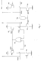
Fig. 2 is a circuit diagram of a conventional circuit 200 implementing part of the FIFO
memory 50 in Fig. 1. Registers 202 and 204 each correspond to one of registers 104 through
107, and control section 206 loosely corresponds to the control elements 110 through 113.
Control section 206 includes serially-connected Muller C elements 208,210, and 212, and
exclusive-OR (XOR) gates 214 and 216.
A Muller C element is a well-known sequential circuit element that reproduces the
value of its input nodes at its output node when the input nodes become logically identical.
For example, if a C-element had inputs (low, low), its output would be low. If the input
nodes changed to (high, low), its output would remain low. The output would change to high
only when the input nodes changed to (high, high). C- elements 208, 210, 212 each have an
inverted upper input (represented by a bubble). Thus, C-elements 208,210, and 212 will
replicate their lower input on their output node when the two inputs differ.
C- elements 208, 210, and 212 are connected so that each C-element takes as one input
the output of the previous (lower) C-element in the chain, and as the other input, the inverted
output of the next (upper) C-element in the chain. Thus, a given C-element changes its output
only when its state is different from the state of the previous C-element and the same as that
of the next C-element in the chain.
XOR gate 216 receives the output of Muller C elements 208 and 210 and drives the
gate input of register 204 with its output. Similarly, XOR gate 214 receives the output of
Muller C element 210 and 212 and drives the gate input of register 202 with its output.
Although Fig. 2 shows only two registers, any number of FIFO stages could be implemented
by correspondingly extending the control section with additional C-elements and XOR gates,
and adding the required number of registers to the data circuitry.
Table I illustrates exemplary timing relationships of the logic states of the circuit
shown in Fig. 2 at the circuit points labeled A, B, C, D, E, F, and G.
| Time Interval | A | B | C | D | E | F | G |
| 0 | low | low | low | low | low | high | low |
| 1 | high | low | low | low | low | high | low |
| 2 | high | high | low | high | low | high | low |
| 3 | high | high | high | low | high | high | low |
| 4 | high | high | high | low | low | high | high |
At time interval 0, point F is high, indicating that the data register below is full and
the value that it contains is present at point H. Points E and D are low, indicating that
registers 202 and 204 are empty. In interval one, C-element 208 changes state so that the
value at point A matches that at point F. Next, the output of C-element 208 propagates to
C-element 210 and the
output D of XOR gate 216 becomes high, indicating that register 204 should latch its input
data (interval two). Also in interval two, output B of C-element 210 becomes high. Since
output B serves as input to C- elements 208 and 212, and to XOR gates 214 and 216, this
change in output B has multiple consequences that appear in interval three.
At time interval three, C-element 212 outputs a high voltage at point C in response to
the high value at point B, since its inverting input from point G is low. Also in response to the
high voltage at point B, output D of XOR gate 216 changes to low, indicating that register
204 is
now empty. In further response to the high voltage at point B, the output E of XOR gate 214
changes to high, indicating that its register 202 is now full. Finally, the high value of point B
is applied to the inverting input of C-element 208, so that it can respond to a subsequent
change in input F from high to low that would announce the availability of a second data
value at the data input to data register 204.
In interval four, output E of XOR gate 214 returns to its original low value as a
consequence of the high value at point C. The low value of point E indicates that its data
register 202 is empty, having passed the first data value on to the next stage of the pipeline,
which is not shown. The initially low value at point G indicated that the next stage of the
pipeline was ready to accept the value of register 202 when point C changed to the high value.
Thus, in interval four, points D and E have returned to their initial low values, indicating
empty. Any time after point A changed from low to high in interval 1, the circuit could
receive a second data value that would be signaled by a change in point F from high to low.
The second and subsequent data values can propagate correctly, in an orderly fashion, though
an unlimited number of pipeline stages of the kind described above.
Correct and efficient movement of the data elements from register 204 to register 202
in Fig. 2 depends on accurate timing of the changes in the register gate signals at points D and
E, so that D drives register 204 empty and E drives register 202 full as soon as possible
without corrupting the data element. Unfortunately, the relative timing of the state changes at
points E and D when point B changes state is subject to the difference of delays in XOR
circuits 214 and 216. XOR gates are relatively complicated circuits that can introduce
significant timing uncertainties into the FIFO memory shown in Fig. 2, and those
uncertainties reduce the maximum safe operating speed of the circuit.
There is, therefore, a need to reduce timing uncertainties in an asynchronous pipeline,
such as a FIFO memory, and to couple control signals more tightly to increase operating
speeds of such pipelines.
The need is even more critical when the timing of data movement is subject to
additional constraints, such as in a counterflow pipeline. Fig. 3 is a block diagram
illustrating a portion of a counterflow pipeline. Counterflow pipeline 300 includes a first
pipeline 320 (called the "instruction pipeline") and a second pipeline 340 (called the "result
pipeline"), which move data elements in opposite directions. In Fig. 3, instruction pipeline
320 moves data elements to the right and result pipeline 340 moves data elements to the left.
The stages of pipeline 320 include serially-connected control sections 328 through 330 and
their corresponding data element storage and operation sections 322 through 324. Each
section 322 through 324 includes memory for storing an instruction and associated
information fields needed to execute the instruction. Data element storage and operation
sections 322 through 324 may include, for example, an ALU capable of executing an integer
instruction.
The stages of pipeline 340 include serially connected control sections 348 through 350
and corresponding result storage elements 342 through 344. The result storage elements store
and transfer data values that result from or are needed for an instruction in one of storage and
operation sections 322 through 324.
In operation, an instruction in each stage of pipeline 320 can interact with a result in
the corresponding stage of pipeline 340. At each stage information in instruction sections 322
through 324 can be compared with information in corresponding result sections 342 through
344, respectively. If, for example, it is determined that section 322 requires as an operand a
result that is in section 342, the result is copied into section 322. On the other hand,
information can similarly be copied or transferred in the reverse direction, from the
instruction pipeline to the results pipeline, where it will move and be available to interact
with following instructions in the instruction pipeline. For correct operation of counterflow
pipeline 300 for this and other applications, each result flowing down pipeline 340 must
interact with each instruction flowing up pipeline 320. Even though the stage in which this
interaction will take place is not known in advance, it is essential that such an interaction
must take place in some stage, or an error will occur. Thus, it is required that the control
circuits do not permit an instruction in pipeline 320 and a result in pipeline 340 to cross any
stage boundary in opposite directions.
Thus, there is a further need and importance for asynchronous control
circuitry having tightly coupled control signals which accurately control sophisticated
pipelines such as a counterflow pipeline.
SUMMARY OF THE INVENTION
Control elements directly dictate the states of the pipeline data storage elements, and
a single detector circuit simultaneously changes the states of the control elements of adjacent
stages. By comparison, in the circuit 206 of Figure 2, control information for data register
204 is stored in two C-elements, 208 and 210, and its full or empty state is determined by
XOR gate 216. Removing XOR circuits from the control elements and implementing the
detection circuitry in a simple signal path common to the preceding and succeeding control
stages significantly reduces timing uncertainties in conventional circuits. The invention is
useful in many different applications, such as asynchronous counterflow pipelines, forking
pipelines, and merging pipelines.
The advantages and purposes in accordance with this the invention will be set forth in
the following description and will also be obvious from the description, or may be learned by
practicing the invention. The advantages and purpose of the invention will be realized and
attained by means of the elements and combinations particularly pointed out in the appended
claims.
To obtain the advantages, and in accordance with the purpose of the invention, as
embodied and broadly described herein, one embodiment includes a circuitry for
controlling an asynchronous counterflow pipeline, including a first
pipeline and a second pipeline flowing in opposite directions, comprising:
BRIEF DESCRIPTION OF THE DRAWINGS
The accompanying drawings, which are incorporated in and constitute a part of this
specification, illustrate several embodiments of the invention and, together with the
description, serve to explain the principles of the invention. In the drawings,
DETAILED DESCRIPTION
Reference will now be made in detail to the embodiments of the invention, examples
of which are illustrated in the accompanying drawings. Wherever possible, the same
reference numbers will be used throughout the drawings to refer to the same or like parts.
This invention includes apparatus for asynchronously controlling a serially-connected
pipeline organized as a first-in-first-out (FIFO) pipeline. The first three embodiments
described below provide fast, simple FIFO pipeline control circuitry allowing relative signal
arrival times at the gates of data storage and transfer elements to be predictably and precisely
controlled. Tightly binding the relative timing of the data storage and transfer elements in
this way increases the FIFO memory operating speed without data corruption. The fourth,
fifth, and sixth embodiments of this invention describe applications using novel modifications
of the third embodiment.
The control circuitry for all embodiments includes an alternating chain of control
circuits and detection circuits. When a control circuit in the Full state precedes a control
circuit in the Empty state, indicating that the data storage element corresponding to the full
control circuit should transfer its data to the next storage element corresponding to the empty
control circuit, the detection circuit generates a "move" signal. The "move" signal sets the
state of the preceding control circuit to Empty and the following control circuit to Full,
thereby enabling movement of a data element from the preceding to the following stage.
Because the control circuits are relatively simple and have predictable signal propagation
times, the relative reaction times of two adjacent control circuits to the common move signal
can be tightly controlled.
Figs. 4-7 show the first embodiment of an asynchronous FIFO according to the
present invention, using a control circuit that stores full/empty state information as charge on
a circuit capacitance. Simulations of this embodiment indicate that data propagation rates
well above 1 GHz are possible using a 0.6 micron CMOS fabrication process.
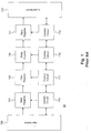
Fig. 4 is a high level block diagram 400 of the first embodiment of the structure of the
asynchronous FIFO pipeline. The diagram shows three stages of the FIFO pipeline for
illustration, although in practice, the FIFO pipeline could have many more stages.
Serially-connected registers 402-404 store and transfer data through each stage of
FIFO pipeline 400. Registers 402-404 transfer data received at input D to output Q when a
signal at their gate input G is active, indicating the register is Empty. When the gate signal is
inactive, registers maintain their data output Q at the last value because they are Full. To
operate properly with the control circuitry, registers 402-404 are arranged to alternate
between active high and active low gate signals. Registers 402 and 404 are driven Full by a
low voltage signal and register 403 is driven Full by a high voltage signal.
Control section 410 includes an alternating series of a first control circuit 411, a first
detection circuit 414, a second control circuit 412, and a second detection circuit 415. Circuit
411 controls the gate input to registers 402 and 404, and circuit 412 controls the gate input to
register 403. Each detection circuit 414 and 415 monitors the states of two adjacent control
circuits and provides a move signal to such circuits whenever a control circuit indicating Full
precedes a control circuit indicating Empty in the chain.
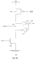
Figs. 5A and 5B are circuit diagrams illustrating control circuits 411 and 412 as used
in the first embodiment. It is possible to construct a similar control section that uses only one
kind of control circuit alternating with one kind of detection circuit, but the circuit 400 shown
in Fig. 4 operates more rapidly and also provides inverters 516 and 526 that simplify addition
of "keeper" circuits that make the circuit capable of static operation, as will be explained.
Control circuit 411 comprises a PMOS transistor 512 connected in series with an NMOS
transistor 514. The Empty/Full state information is stored at node 515 as charge on
surrounding circuit capacitance, which includes gate capacitance from inverter 516 and
capacitance due to various diffusion and wiring stray capacitances.
PMOS transistor 512 is turned on by placing its gate Set
E (set Empty) ("
"
indicates active low) to the low state, and
NMOS transistor 514 is turned on by placing its
gate input Set F (set Full) to the high state. Turning
transistor 512 on while
transistor 514 is
off
sets node 515 to Vdd (high), and turning
transistor 514 on while
transistor 512 is
offsets
node 515 to ground (low).
Inverters 516 and 517 are connected in a "circular" arrangement between node 515
and the Full output of circuit 411. Inverter 517 functions as a "keeper" inverter that replaces
charge leaking from node 515 when both transistors 512 and 514 are turned off. Without
keeper inverter 517, node 515 would lose its charge state due to leakage current, and require
recharging by periodically turning on one of transistors 512 and 514. Keeper inverter 517
thus preserves the state of node 515, even when the pipeline is inactive for long periods; such
a circuit is called "static". The keeper inverter 517 may be omitted if it is known that the
pipeline will always be operated at sufficiently short intervals; such a circuit is called
"dynamic".
Keeper inverter 517 is a "weak" inverter that can provide only a small amount of
output current relative to PMOS transistor 512 and NMOS transistor 514. Typically, the
width of the transistors in keeper inverter 517 may approximately 10-20 times smaller than
the width of those in inverter 516. For example, keeper inverter 517 may have a width of
about 1.2 microns for both its P and N channel transistors, while inverter 516 has a width of
about 24 microns for its P-channel transistors and 12 microns for its N-channel transistors. In
comparison, transistors 512 and 514 may have widths of approximately 36 microns and 18
microns, respectively.
Control circuit 412, shown in Fig. 5B, comprises
PMOS transistor 522,
NMOS
transistor 524,
inverter 526, and
keeper inverter 527.
Circuit 412 is a structurally identical,
but mirror image of
circuit 411. In
circuit 412, however, the gate inputs at the PMOS and
NMOS transistors and the output are assigned different meanings than the corresponding
structure in
circuit 411. In particular, in
circuit 412, the gate of
transistor 522 is designated
Set
F and the gate of
transistor 524 is designated Set E. Additionally, a high voltage at the
left output 528 of
inverter 526 indicates Empty, and a high voltage at the right output
indicates Full.
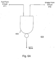
Figure 6A is a circuit diagram of a preferred embodiment of
detection circuitry 414 as
a
NAND gate 600 receiving as input the
Full output 518 of
circuit 411 and the
Empty output
528 of
circuit 412. The output of detection circuit 414 (i.e. the Move
signal) is input to the
Set
E input of
circuit 411 and the Set
F input of
circuit 412.
Detection circuitry 414 operates
to detect the Full condition of
circuit 411, expressed by a high value on
node 518, and the
Empty condition of
circuit 412, expressed as a high value on
node 528.
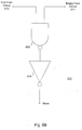
Figure 6B is a circuit diagram of a preferred embodiment of detection circuit 415 as a
NAND gate 602 receiving as inputs the Full output 525 of circuit 412 and the Empty output
515 of circuit 411, and an inverter 604 connected to the output of NAND gate 602. The
output of inverter 604 (i.e. the move signal) is input to the Set E input of circuit 412 and the
Set F input of circuit 411. Detection circuit 415 detects the Full condition of circuit 412,
expressed by a high value of node 525, and the Empty condition of circuit 411, expressed by a
high value of node 515 of circuit 411.
Fig. 7 is a circuit diagram illustrating a portion of control section 410 shown in Figs.
4, 5, and 6, redrawn as a single figure. For simplicity and ease of understanding the circuit
operation, inverters 516 and 526 and detection circuit 414 are shown as their logically
equivalent OR gate 707, and the detection circuit 415 is shown as its logically equivalent
AND gate 708. Transistors 704, 705, and 706 are PMOS transistors and transistors 701, 702,
and 703 are NMOS transistors.
To demonstrate the operation of this circuit, we start with the assumption that nodes
A, B and C have values of low, high, and high, respectively. This corresponds to the Full,
Full and Empty states. Since the values at nodes B and C are both high, AND gate 708
applies a high level to the gate of the two opposing NMOS transistors 702 and 703. This
turns transistors 702
and 703 on and sets nodes B and C low. The circuit states of nodes A, B and C at this
intermediate step now indicate the conditions Full, Empty, Full, respectively. Thus, the full
condition expressed by node B has moved to node C, and the empty condition expressed by
node C has moved to node B. These changes of circuit states B and C are coupled to the gate
inputs
of the associated data registers, producing a corresponding movement of the data value held
in the data register associated with node B to the data register associated with node C.
A next step now occurs when the new low level at node B reaches OR gate 707,
which continues to receive a low input from node A. The output of OR gate 707 applies a low
level to the gates of PMOS transistors 705 and 706, turning them on and setting nodes A and
B high.
After this step, nodes A, B and C express the values Empty, Full, Full, respectively. The Full
values originally expressed by nodes A and B have both moved to the right, into nodes B and
C, so that the data value originally held in the data register associated with node A is now
held in the data register associated with node B, whose contents have in turn been moved to
the data register associated with node C.
In a similar fashion, data values associated with node C can move to the right into
subsequent stages of the pipeline, and new data values can flow into the stage associated with
node A from additional stages extending to the left of stage A. Repetition of such cycles of
operation, each cycle involving interactions only between neighboring stages, moves data
elements to the right through the pipeline so long as there are empty cells available to hold
them.
Although the preferred embodiment has been described using registers as the data
storage and transfer elements, many equivalent implementations could also be used.
Additionally, amplification of control signals G and G
, shown in Fig. 4, through one or more
buffer stages may be needed when multiple data registers are driven to permit movement of
data with multiple bits. Furthermore, instead of using registers with alternating gate
polarities, the buffer stages may be arranged to invert the gate polarity.
Figs. 8 and 9 show a second embodiment for the control structure of an asynchronous
FIFO memory according to this invention. This embodiment is similar to the embodiment in
Figs. 4-7 in that asynchronous FIFO memory 800 stores its data elements in serially-connected
data registers 802, 803, and 804. In Figs. 8 and 9, however, each stage has
identical control circuitry (set-reset latches 806) and detection circuitry (logic gates 810).
Registers 802 through 804 receive data at input D and transfer the received data to the
output Q according to the signal at gate input G. Gate input G of each flip-flop 802 through
804 connects to the Full (F) output of set-reset latches 806. Logic gates 81'0 receive as inputs
the Full output of one set-reset latch 806 and the Empty output of a succeeding set-reset latch
806.
In normal operation, the Full and Empty outputs of latches 806 are static complements
of one another. A high logic state at the Full output of the set-reset latch driving data register
803 causes data register 803 to retain the present value of its output Q, which is connected to
the data input D of the next data register 804. Alternatively, a low logic state at the Full
output of the set-reset latch causes data register 803 to unlatch the present value of its data
output Q, thereby allowing data register 803 to receive a new data value from its preceding
data register 802 and pass this new data value to the data input D of the succeeding data
register 804.
Logic gates 810 are preferably NAND gates, but may be other logic depending
on the particular implementation of the set-reset latches. In operation, logic gates 810 receive
the Full output signal of the preceding set-reset latch and the Empty output signal of the
succeeding set-reset latch, and when both are present, the output of the NAND gate becomes
low. It then drives the preceding set-reset latch from the Full state to the Empty state, and the
succeeding set-reset latch from the Empty state to the Full state, thereby initiating the
unlatching of the preceding data register and the latching of the succeeding data register.
These actions move a data value held in the preceding data register into the succeeding data
register, and make the preceding register ready to accept its next data value.
Whenever the preceding set-reset latch reaches the Empty state, or the succeeding
set-reset latch reaches the Full state, logic gate 810 is no longer activated, and the output of
the NAND gate becomes high, thereby no longer driving the preceding or succeeding set-reset
latches to the Empty and Full states, respectively. If necessary, additional circuit delay
elements may be inserted into the set-reset latches and in logic gates 810 so that these steps
are properly coordinated.
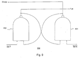
Fig. 9 is a preferred circuit diagram of set-
reset latch 806.
NAND gate 902 and
NAND gate 904 are cross-coupled so
NAND gate 902 receives the Set-F signal at one input
and the output of
NAND gate 904 at its second input.
NAND gate 904 receives the Set
E
signal at its second input and the output of
NAND gate 902 at its first input.
The set-reset latches and logic gate 910 may also be implemented with NOR gates
instead of NAND gates, but NAND gates are more efficient in silicon implementations using
known manufacturing techniques.
Table II illustrates exemplary timing relationships of two neighboring set-reset latches
806 and
logic gate 810. Columns A through E in Table II correspond to the points labeled A
through E in Fig. 8.
| Time Interval | A | B | C | D | E | Description |
| 0 | high | low | low | high | X | First latch is full, its succeeding latch is empty. |
| 1 | high | low | low | high | low | The high values at A and D cause the NAND gate to become low. |
| 2 | high | high | high | high | low | The low value at the output of the NAND gate causes the set-reset latches to begin to toggle. At this point, the states at points B and C have changed. |
| 3 | low | high | high | low | low | The set-reset latches finish changing. |
| 4 | low | high | high | low | high | The low values at A and D cause the NAND gate to become high. Circuit is now in a steady-state. |
At time interval zero, the initial state, points A and D are high, and B and C are low.
This corresponds to the first latch indicating the Full state (A is high) and the second latch
indicating the Empty state (C is low). Table II shows the signals asynchronously propagating
through the circuit until the first latch becomes Empty (A is low) and the second latch
becomes Full (C is high).
Fig. 10 is a block diagram illustrating a control structure for an asynchronous FIFO
memory according to a third embodiment. As with the second embodiment, FIFO memory
1000 stores its data elements in serially-connected registers 802 through 804 controlled by
control circuitry (set-reset latches) 806 and detection circuitry (a logic NAND gate) 810.
Unlike FIFO memory 800, however, FIFO memory 1000 includes two additional inverters,
1002 and 1004, per stage. Also, instead of connecting the Full output from the previous stage
and the Empty output from the succeeding stage to input of logic gate 810, in FIFO memory
1000 the Empty output from the previous stage and the Full output from the succeeding stage
are connected through inverters 1002 and 1004, respectively, to the input of logic gate 810.
FIFO memory 1000 operates similarly to FIFO memory 800. Because the Full and
Empty outputs of set-reset latch 806 operate as static-state complements of one another, the
inverted inputs to logic gates 810, as used in FIFO memory 1000, are logically equivalent to
the noninverted inputs entering logic gates 810 in FIFO memory 800.
Although the static-state analysis of set-reset latch 806 indicates that outputs E and F
are logical complements, this is not necessarily true while the state of the latch is changing
states. Simulations of long pipelines (64 or more stages) of FIFO memory 800 indicate that
losses of information may occur after data have propagated through many stages. Such losses
appear to result from set-reset latches 806 and NAND gates 810 reaching pathological control
states.
The control circuit used in FIFO 1000, unlike that of FIFO 800, does not possess
control states other than those accessed in normal operation. The difference arises from
inverters 1002 and 1004 generating a high signal at the input of NAND gates 810. Inverter
1002 receives its input from output E of set-reset latch 806 and inverter 1004 receives its
input from output F of the succeeding set-reset latch 806. In the control circuit for FIFO 800,
the corresponding input to NAND gates 810 come directly from the F output of set-reset latch
806 and the E output of the succeeding set-reset latch 806.
Although ordinary logical analysis indicates that the two circuits are logically
equivalent in the static condition, simulations of long FIFO chains using control circuit 1000
have shown reliable operation. These simulations have been confirmed by tests on
experimental circuits fabricated using a 0.6 micron CMOS process. The experimental chips
have operated at up to about 1 GHz without data loss.
The principles discussed above may be used to control more complex asynchronous
circuits.
Asynchronous pipeline control circuitry, in accordance with this invention, capable of
controlling a counterflow pipeline will next be described with reference to Figs. 11 and 12.
The basic design of this control circuitry is similar to that used in the third embodiment.
Because a counterflow pipeline comprises two pipelines flowing in opposite directions, two
control circuits are required-- one for each pipeline. Generally, each control circuit operates
independent of the other control circuit, moving their corresponding data elements when one
stage is Full and the succeeding stage is Empty. However, in this embodiment, the control
circuitry corresponding to each pipeline additionally interacts with one another to prohibit
data elements in the two pipelines from simultaneously passing one another.
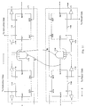
Fig. 11 is a circuit diagram of asynchronous pipeline control circuitry capable of
controlling a counterflow pipeline according to a fourth embodiment of the invention.
Control circuitry 1110 controls the movement of data elements through the first pipeline (the
instruction pipeline), and includes
logic gate 1112, set-
reset latches 1114 and 1116, and
inverters 1118 and 1119.
Logic gate 1112 receives the inverted Full output of set-
reset latch
1116 and the inverted Empty output of set-
reset latch 1114. The output of
logic gate 1112 is
input to the Set
E and Set
F inputs of
latches 1114 and 1116, respectively. Additionally,
unlike the third embodiment, in this embodiment, the output of the opposing gate logic 1122
(labeled as output B) is received by
logic gate 1112, the Set E input of set-
reset latch 1114,
and the Set F input of set-
reset latch 1116.
Control circuitry 1120 controls the movement of data elements through the second
pipeline (the result pipeline), and includes logic gate 1122, set- reset latches 1124 and 1126,
and inverters 1128 and 1129. Logic gate 1122, set-reset latch 1124, and set-reset latch 1126
are arranged similarly to that in control circuitry 1110. In particular, the output of the
opposing logic gate 1112 (labeled as output A) is received by gate logic 1122, the Set E input
of set-reset latch 1120, and the Set F input of set-reset latch 1124.
The operation of control circuitry 1110 and 1120 may be conceptualized as occurring
in two modes. The first mode of operation occurs when a Full value is ready to propagate
through either one but not both of set-reset latches 1114 or 1126 to the next (Empty) set- reset
latch 1116 or 1124. For example: if output E on set-reset latch 1114 is low, indicating this
latch is Full; the output F on set-reset latch is low, indicating this latch is empty; and the
signal at point B is high, indicating control circuit 1120 is not ready to propagate data
elements, NAND gate 1112 changes its output at point A to low, causing set- reset latches
1114 and 1116 to each change states. The low value at point A disables set- reset latches 1124
and 1126 from changing states by "locking" NAND gate 1122 to a high value. Therefore,
even if set- reset latches 1124 and 1126 subsequently change state so that set-reset latch 1126
is Full and set-reset latch 1124 is Empty, the Full state of latch 1126 will not propagate to the
Empty state of latch 1124 until NAND gate 1112 "unlocks" NAND gate 1122.
The second mode of operation occurs when both sets of set-reset latches become
ready to transfer data at the same time. In this situation, both NAND gates 1112 and 1122
receive high values on their three inputs simultaneously, or nearly simultaneously, causing
them to enter a metastable operation state. In the metastable state, the outputs of NAND
gates 1112 and 1122 are indeterminate between a logic high voltage and a logic low voltage.
Eventually, the metastable condition will resolve itself and one of the NAND gates will
become low and the other will become high. The NAND gate that becomes low signals its
set-reset latches to change state and locks the "losing" NAND gate high. For proper circuit
operation, set-reset latches 1114, 1116, 1124, and 1126 should not react to the intermediate
voltages present at points A and B in the metastable condition. This is achieved by the use of
a modified set-reset latch circuit.
Fig. 12 is a preferred circuit diagram 1200 of modified set-reset latches 1114, 1116,
1124, and 1126. Set-reset latch 1200 comprises two modified cross-coupled NAND gates
1202 and 1204. Conventional NAND gates are identical to modified NAND gates 1202 and
1204, except that in a conventional NAND gate, the Set F input on NAND gate 1202 and the
Set E input on NAND gate 1204 are coupled to Vdd. By coupling the source of PMOS
transistor 1206 to Set F and the source of PMOS transistor 1210 to Set E, modified NAND
gates 1202 and 1204 do not react until the voltages at points A and B in Fig. 11 are
sufficiently different to exceed the threshold voltages of PMOS transistors 1206 and 1210 in
the proper direction. In a metastable condition of circuits 1112 and 1122, the voltages at
point A and point B are approximately the same, and remain so until the metastable condition
resolves. Thus, set-reset latches 1124,1126,1114, and 1116 will wait until a metastable state
at NAND gates 1122 and 1112 resolves itself and the voltages at points A and B become
sufficiently different before changing state. Because the connections of point A and point B
to set-reset latches 1114-1116 and 1126-1124 are reversed, a move action will occur in only
one of the pipelines. Only when the move signal for that pipeline is removed will the other
pipeline be able to execute its move.
Modified NAND gate 1202 comprises PMOS transistors 1206 and 1213, and NMOS
transistors 1207 and 1208. The output of NAND gate 1202 represents the Full condition of
set-reset latch 1200 and emanates from the terminal common to transistors 1206, 1207, and
1213. The two gate controlling inputs to the NAND gate are Set-F, which is received at the
gates of transistors 1206 and 1207, and the output of NAND gate 1204, which is received at
the gates of transistors 1213 and 1208.
Modified NAND gate 1204 is an identical mirror image of NAND gate 1202. NAND
gate 1204 comprises PMOS transistors 1209 and 1210, and NMOS transistors 1211 and 1212.
The output of NAND gate 1204 represents the Empty condition of set-reset latch 1200 and
the two gate controlling inputs to the NAND gate are Set-E and the output of NAND gate
1202.
In addition to a counterflow pipeline, the principles described above in connection
with the first three embodiments may also be used to control forking and merging pipelines.
Asynchronous pipeline control circuitry capable of controlling forking and merging
pipelines will next be described with reference to Figs. 13-16. Figs. 13A and 13B are
conceptual diagrams illustrating two stages of a forking pipeline and two stages of a merging
pipeline, respectively. In both figures, data flows from the left to the right. The control logic
denning data movement between stages in forking pipeline 1300 is as follows: move the data
in stage 1306 to stages 1302 and 1304 when stage 1306 is Full and both stages 1302 and 1304
are Empty. Conversely, the control logic defining data movement in merging pipeline 1310
is: move data from stages 1312 and 1314 into stage 1316 when both stages 1312 and 1314 are
Full and stage 1316 is Empty.
Fig. 14 is a block diagram illustrating pipeline control circuitry for a forking
asynchronous pipeline according to a fifth embodiment. Stage 1401, the pre-fork stage,
corresponds to stage 1306 in Fig 13A.
Stages 1403 and 1405, the post-fork stages,
corresponds to
stages 1302 and 1304, respectively. Each
stage 1401, 1403, and 1405 includes
set-reset latches 1402, one of
registers 1404 through 1406, and
inverters 1408 and 1410.
This structure is identical to set-
latches 806,
registers 802 through 804, and
inverters 1002
and 1004, as used in the third embodiment.
Detection circuitry 1412, however, is a three-input
NAND gate whereas the third embodiment has two-
input NAND gate 810. The output
of
NAND gate 1406 is input to the Set
E input of the pre-fork set-reset latch and to the Set
F
input of the post-fork set-reset latches.
Similar to the third embodiment, in this embodiment, a common move signal
generated by NAND gate 1412 causes the pre-fork set-reset latch to become Empty and the
post-fork set-reset latches to become Full. Concomitant with latches 1402 changing state, the
data in register 1404 transfers to registers 1405 and 1406.
Fig. 15 is a block diagram illustrating pipeline control circuitry for a merging
asynchronous pipeline according to a sixth embodiment. The control logic for the merging
pipeline is essentially a mirror image of the control logic for the forking pipeline. Stages
1501 and 1503 are the pre-merge stages, corresponding to stage 1312 and 1314 in Fig 13B,
and stage 1505 is the post-merge stages, corresponding to stage 1316.
Similar to the third embodiment, in this embodiment, a common move signal
generated by NAND gate 1412 causes the pre-merge set-reset latches to change to Empty and
the post-merge set-reset latches to become Full. Concomitant with latches 1402 changing
state, the data in registers 1404 and 1405 transfers to register 1506. In this example, registers
1404 and 1405 are 4 bit registers and register 1506 is an eight bit register.
Although a two-pronged pipeline fork/merge using a three input NAND gate has been
described, one could implement a three-pronged or greater pipeline fork/merge with a four
input or greater NAND gate and additional pipeline stages. Additionally, although the sixth
embodiment merged two four bit data elements into an eight bit data element, logic may
operate on the two four bit streams and output a single four bit stream or perform other
functions such as the four-bit sum of two four-bit data elements from the two merging
pipelines.
As the previous discussion explains in detail, by tightly binding the relative timing of
asynchronous pipeline control and transfer elements, pipeline operating speed can be
significantly increased. Three basic embodiments have been disclosed for performing such
binding. Further, extensions of these principles have been described for counterflow
pipelines, forking pipelines, and merging pipelines. The insertion of circuitry between data
registers to calculate functions of pipeline data has been disclosed and can be applied in many
ways.
It will be apparent to those skilled in the art that various modifications and variations
can be made to the present invention without departing from the scope or spirit of the
invention. For example, although the embodiments describe FIFO circuits devoid of logic for
processing the data elements as they pass from data register to data register, one could insert
processing logic between the FIFO memory stages to create a pipelined data processor.