EP1296383A2 - Beleuchtungseinheit mit mindestens einer LED als Lichtquelle - Google Patents
Beleuchtungseinheit mit mindestens einer LED als Lichtquelle Download PDFInfo
- Publication number
- EP1296383A2 EP1296383A2 EP02015876A EP02015876A EP1296383A2 EP 1296383 A2 EP1296383 A2 EP 1296383A2 EP 02015876 A EP02015876 A EP 02015876A EP 02015876 A EP02015876 A EP 02015876A EP 1296383 A2 EP1296383 A2 EP 1296383A2
- Authority
- EP
- European Patent Office
- Prior art keywords
- lighting unit
- unit according
- led
- phosphor
- radiation
- Prior art date
- Legal status (The legal status is an assumption and is not a legal conclusion. Google has not performed a legal analysis and makes no representation as to the accuracy of the status listed.)
- Withdrawn
Links
Images


Classifications
-
- H—ELECTRICITY
- H01—ELECTRIC ELEMENTS
- H01L—SEMICONDUCTOR DEVICES NOT COVERED BY CLASS H10
- H01L33/00—Semiconductor devices with at least one potential-jump barrier or surface barrier specially adapted for light emission; Processes or apparatus specially adapted for the manufacture or treatment thereof or of parts thereof; Details thereof
- H01L33/48—Semiconductor devices with at least one potential-jump barrier or surface barrier specially adapted for light emission; Processes or apparatus specially adapted for the manufacture or treatment thereof or of parts thereof; Details thereof characterised by the semiconductor body packages
- H01L33/50—Wavelength conversion elements
- H01L33/501—Wavelength conversion elements characterised by the materials, e.g. binder
- H01L33/502—Wavelength conversion materials
-
- C—CHEMISTRY; METALLURGY
- C09—DYES; PAINTS; POLISHES; NATURAL RESINS; ADHESIVES; COMPOSITIONS NOT OTHERWISE PROVIDED FOR; APPLICATIONS OF MATERIALS NOT OTHERWISE PROVIDED FOR
- C09K—MATERIALS FOR MISCELLANEOUS APPLICATIONS, NOT PROVIDED FOR ELSEWHERE
- C09K11/00—Luminescent, e.g. electroluminescent, chemiluminescent materials
- C09K11/08—Luminescent, e.g. electroluminescent, chemiluminescent materials containing inorganic luminescent materials
- C09K11/0883—Arsenides; Nitrides; Phosphides
-
- C—CHEMISTRY; METALLURGY
- C09—DYES; PAINTS; POLISHES; NATURAL RESINS; ADHESIVES; COMPOSITIONS NOT OTHERWISE PROVIDED FOR; APPLICATIONS OF MATERIALS NOT OTHERWISE PROVIDED FOR
- C09K—MATERIALS FOR MISCELLANEOUS APPLICATIONS, NOT PROVIDED FOR ELSEWHERE
- C09K11/00—Luminescent, e.g. electroluminescent, chemiluminescent materials
- C09K11/08—Luminescent, e.g. electroluminescent, chemiluminescent materials containing inorganic luminescent materials
- C09K11/77—Luminescent, e.g. electroluminescent, chemiluminescent materials containing inorganic luminescent materials containing rare earth metals
- C09K11/7715—Luminescent, e.g. electroluminescent, chemiluminescent materials containing inorganic luminescent materials containing rare earth metals containing cerium
- C09K11/77218—Silicon Aluminium Nitrides or Silicon Aluminium Oxynitrides
-
- F—MECHANICAL ENGINEERING; LIGHTING; HEATING; WEAPONS; BLASTING
- F21—LIGHTING
- F21K—NON-ELECTRIC LIGHT SOURCES USING LUMINESCENCE; LIGHT SOURCES USING ELECTROCHEMILUMINESCENCE; LIGHT SOURCES USING CHARGES OF COMBUSTIBLE MATERIAL; LIGHT SOURCES USING SEMICONDUCTOR DEVICES AS LIGHT-GENERATING ELEMENTS; LIGHT SOURCES NOT OTHERWISE PROVIDED FOR
- F21K9/00—Light sources using semiconductor devices as light-generating elements, e.g. using light-emitting diodes [LED] or lasers
- F21K9/60—Optical arrangements integrated in the light source, e.g. for improving the colour rendering index or the light extraction
- F21K9/64—Optical arrangements integrated in the light source, e.g. for improving the colour rendering index or the light extraction using wavelength conversion means distinct or spaced from the light-generating element, e.g. a remote phosphor layer
-
- H—ELECTRICITY
- H01—ELECTRIC ELEMENTS
- H01L—SEMICONDUCTOR DEVICES NOT COVERED BY CLASS H10
- H01L2224/00—Indexing scheme for arrangements for connecting or disconnecting semiconductor or solid-state bodies and methods related thereto as covered by H01L24/00
- H01L2224/01—Means for bonding being attached to, or being formed on, the surface to be connected, e.g. chip-to-package, die-attach, "first-level" interconnects; Manufacturing methods related thereto
- H01L2224/26—Layer connectors, e.g. plate connectors, solder or adhesive layers; Manufacturing methods related thereto
- H01L2224/31—Structure, shape, material or disposition of the layer connectors after the connecting process
- H01L2224/32—Structure, shape, material or disposition of the layer connectors after the connecting process of an individual layer connector
- H01L2224/321—Disposition
- H01L2224/32151—Disposition the layer connector connecting between a semiconductor or solid-state body and an item not being a semiconductor or solid-state body, e.g. chip-to-substrate, chip-to-passive
- H01L2224/32221—Disposition the layer connector connecting between a semiconductor or solid-state body and an item not being a semiconductor or solid-state body, e.g. chip-to-substrate, chip-to-passive the body and the item being stacked
- H01L2224/32245—Disposition the layer connector connecting between a semiconductor or solid-state body and an item not being a semiconductor or solid-state body, e.g. chip-to-substrate, chip-to-passive the body and the item being stacked the item being metallic
-
- H—ELECTRICITY
- H01—ELECTRIC ELEMENTS
- H01L—SEMICONDUCTOR DEVICES NOT COVERED BY CLASS H10
- H01L2224/00—Indexing scheme for arrangements for connecting or disconnecting semiconductor or solid-state bodies and methods related thereto as covered by H01L24/00
- H01L2224/01—Means for bonding being attached to, or being formed on, the surface to be connected, e.g. chip-to-package, die-attach, "first-level" interconnects; Manufacturing methods related thereto
- H01L2224/42—Wire connectors; Manufacturing methods related thereto
- H01L2224/47—Structure, shape, material or disposition of the wire connectors after the connecting process
- H01L2224/48—Structure, shape, material or disposition of the wire connectors after the connecting process of an individual wire connector
- H01L2224/4805—Shape
- H01L2224/4809—Loop shape
- H01L2224/48091—Arched
-
- H—ELECTRICITY
- H01—ELECTRIC ELEMENTS
- H01L—SEMICONDUCTOR DEVICES NOT COVERED BY CLASS H10
- H01L2224/00—Indexing scheme for arrangements for connecting or disconnecting semiconductor or solid-state bodies and methods related thereto as covered by H01L24/00
- H01L2224/01—Means for bonding being attached to, or being formed on, the surface to be connected, e.g. chip-to-package, die-attach, "first-level" interconnects; Manufacturing methods related thereto
- H01L2224/42—Wire connectors; Manufacturing methods related thereto
- H01L2224/47—Structure, shape, material or disposition of the wire connectors after the connecting process
- H01L2224/48—Structure, shape, material or disposition of the wire connectors after the connecting process of an individual wire connector
- H01L2224/481—Disposition
- H01L2224/48151—Connecting between a semiconductor or solid-state body and an item not being a semiconductor or solid-state body, e.g. chip-to-substrate, chip-to-passive
- H01L2224/48221—Connecting between a semiconductor or solid-state body and an item not being a semiconductor or solid-state body, e.g. chip-to-substrate, chip-to-passive the body and the item being stacked
- H01L2224/48245—Connecting between a semiconductor or solid-state body and an item not being a semiconductor or solid-state body, e.g. chip-to-substrate, chip-to-passive the body and the item being stacked the item being metallic
- H01L2224/48247—Connecting between a semiconductor or solid-state body and an item not being a semiconductor or solid-state body, e.g. chip-to-substrate, chip-to-passive the body and the item being stacked the item being metallic connecting the wire to a bond pad of the item
-
- H—ELECTRICITY
- H01—ELECTRIC ELEMENTS
- H01L—SEMICONDUCTOR DEVICES NOT COVERED BY CLASS H10
- H01L2224/00—Indexing scheme for arrangements for connecting or disconnecting semiconductor or solid-state bodies and methods related thereto as covered by H01L24/00
- H01L2224/01—Means for bonding being attached to, or being formed on, the surface to be connected, e.g. chip-to-package, die-attach, "first-level" interconnects; Manufacturing methods related thereto
- H01L2224/42—Wire connectors; Manufacturing methods related thereto
- H01L2224/47—Structure, shape, material or disposition of the wire connectors after the connecting process
- H01L2224/48—Structure, shape, material or disposition of the wire connectors after the connecting process of an individual wire connector
- H01L2224/484—Connecting portions
- H01L2224/4847—Connecting portions the connecting portion on the bonding area of the semiconductor or solid-state body being a wedge bond
- H01L2224/48472—Connecting portions the connecting portion on the bonding area of the semiconductor or solid-state body being a wedge bond the other connecting portion not on the bonding area also being a wedge bond, i.e. wedge-to-wedge
-
- H—ELECTRICITY
- H01—ELECTRIC ELEMENTS
- H01L—SEMICONDUCTOR DEVICES NOT COVERED BY CLASS H10
- H01L2224/00—Indexing scheme for arrangements for connecting or disconnecting semiconductor or solid-state bodies and methods related thereto as covered by H01L24/00
- H01L2224/73—Means for bonding being of different types provided for in two or more of groups H01L2224/10, H01L2224/18, H01L2224/26, H01L2224/34, H01L2224/42, H01L2224/50, H01L2224/63, H01L2224/71
- H01L2224/732—Location after the connecting process
- H01L2224/73251—Location after the connecting process on different surfaces
- H01L2224/73265—Layer and wire connectors
-
- H—ELECTRICITY
- H01—ELECTRIC ELEMENTS
- H01L—SEMICONDUCTOR DEVICES NOT COVERED BY CLASS H10
- H01L2924/00—Indexing scheme for arrangements or methods for connecting or disconnecting semiconductor or solid-state bodies as covered by H01L24/00
- H01L2924/01—Chemical elements
- H01L2924/01068—Erbium [Er]
-
- H—ELECTRICITY
- H01—ELECTRIC ELEMENTS
- H01L—SEMICONDUCTOR DEVICES NOT COVERED BY CLASS H10
- H01L2924/00—Indexing scheme for arrangements or methods for connecting or disconnecting semiconductor or solid-state bodies as covered by H01L24/00
- H01L2924/10—Details of semiconductor or other solid state devices to be connected
- H01L2924/11—Device type
- H01L2924/12—Passive devices, e.g. 2 terminal devices
- H01L2924/1204—Optical Diode
- H01L2924/12041—LED
-
- H—ELECTRICITY
- H01—ELECTRIC ELEMENTS
- H01L—SEMICONDUCTOR DEVICES NOT COVERED BY CLASS H10
- H01L2924/00—Indexing scheme for arrangements or methods for connecting or disconnecting semiconductor or solid-state bodies as covered by H01L24/00
- H01L2924/15—Details of package parts other than the semiconductor or other solid state devices to be connected
- H01L2924/181—Encapsulation
-
- Y—GENERAL TAGGING OF NEW TECHNOLOGICAL DEVELOPMENTS; GENERAL TAGGING OF CROSS-SECTIONAL TECHNOLOGIES SPANNING OVER SEVERAL SECTIONS OF THE IPC; TECHNICAL SUBJECTS COVERED BY FORMER USPC CROSS-REFERENCE ART COLLECTIONS [XRACs] AND DIGESTS
- Y02—TECHNOLOGIES OR APPLICATIONS FOR MITIGATION OR ADAPTATION AGAINST CLIMATE CHANGE
- Y02B—CLIMATE CHANGE MITIGATION TECHNOLOGIES RELATED TO BUILDINGS, e.g. HOUSING, HOUSE APPLIANCES OR RELATED END-USER APPLICATIONS
- Y02B20/00—Energy efficient lighting technologies, e.g. halogen lamps or gas discharge lamps
Definitions
- the invention is based on a lighting unit with at least one LED as Light source according to the preamble of claim 1. It is in particular around a LED emitting in the visible or white based on a primary UV emitting LED.
- a lighting unit with at least one LED as a light source which emits white light, for example, is currently predominantly realized by combining a Ga (In) N LED emitting in the blue at about 460 nm and a yellow-emitting YAG: Ce 3+ phosphor (US 5,998,925 and EP 862,794).
- YAG: Ce 3+ phosphor US 5,998,925 and EP 862,794.
- Two different yellow phosphors are often used for good color rendering, as described in WO-A 01/08453. The problem here is that the two phosphors often show different temperature behavior, even if their structure is similar.
- a well-known example is the yellow luminescent Ce-doped Y-garnet (YAG: Ce) and the long-wave luminescent (Y, Gd) garnet in comparison. This leads to color fluctuations and changes in color rendering at different operating temperatures.
- Ca is preferably used alone for the cation M.
- the Ce portion which replaces part of the cation M should be 0.5 to 15%, preferred 1 to 10%, in particular 2 to 6%, of the M cation lie, which makes a particularly exact choice of the emission wavelength can be made and also the luminous efficacy can be optimized.
- An increasing Ce content generally causes a shift in peak emission towards longer wavelengths.
- This phosphor in connection with an LED-based lighting unit is its high efficiency, its outstanding temperature stability (no sensitivity to changes in operating temperature) and a surprising one high quenching temperature of the luminescence and the high achievable with it Color rendering, especially when combined with at least one other Phosphor.
- the quenching temperature i.e. the temperature at which the luminescence due to the heat supplied is even so high that it is outside of the preselected measuring range (maximum 140 ° C).
- this class of phosphor is that the starting material (in particular Si 3 N 4 ) is already in finely dispersed form. This phosphor therefore no longer has to be ground, which saves one work step and there are no losses in efficiency. Typical average grain sizes of the phosphor are 0.5 to 5 ⁇ m. In contrast, conventional phosphors such as YAG: Ce must be ground so that they remain dispersed in the casting resin and do not sink to the bottom. This grinding process often leads to loss of efficiency. Despite the fine grain size of the starting material, the phosphor according to the invention has good absorption.
- an LED In addition to the generation of a colored light source by excitation using UV radiation an LED mainly offers the generation of white light with the help of this Fluorescent advantages. This happens as the primary for a UV-emitting LED Light source using at least three phosphors.
- White light with good color rendering is particularly generated by the combination a UV-LED (e.g. primary emission at 300 to 430 nm, preferably 380 to 420 nm), a green phosphor according to the invention (emission between 495-540 nm) and one blue (emission: 440-480 nm) and one red-emitting phosphor (Emission: 560-620 nm).
- a UV-LED e.g. primary emission at 300 to 430 nm, preferably 380 to 420 nm
- a green phosphor according to the invention emission between 495-540 nm
- one blue emission: 440-480 nm
- red-emitting phosphor Emission: 560-620 nm
- M Ca is individual or in combination with Sr, the Sr content is preferably less than 30 mol%.
- This green phosphor has excellent thermal stability and shows excellent luminescence behavior at higher temperatures, which are typical for LEDs: up to 80 ° C, it shows no decrease in luminescence within the scope of the measurement accuracy.
- the conventional garnet phosphors show a clearly measurable decrease in luminescence at 80 ° C: it can be 5 to 30%, depending on the selected cation composition in the system (Y, Gd, Lu) 3 (Al, Ga) 5 O 12 ,
- Ce-sialons have pronounced stability against hot acids, bases and also their thermal and mechanical stability. Surprisingly, these sialons show excellent temperature quenching behavior of the luminescence of activator ions in these compounds. This makes these compounds strong competitors for luminescent materials, which sometimes shine brighter and / or more efficiently at room temperature, but show luminescence loss due to temperature quenching.
- the blue-green glowing Sr 4 Al 14 O 25 : Eu 2+ has a quantum efficiency of around 85% at room temperature. At 100 ° C, however, the efficiency has dropped to around 60%.
- Thiogallates, doped with Eu 2+ , depending on their cation composition can luminesce in the entire green area, also lose 20% -30%.
- Yellow luminescent Ce 3+ -doped garnets lose around 10-30% of the efficiency at room temperature, depending on the proportion of Gd: Y and Al: Ga at high temperature.
- a white mixture can be produced on the basis of a UV-emitting LED using these Ce-doped sialons together with a blue phosphor, such as BaMgAl 10 O 17 : Eu 2+ (BAM), Ba 5 SiO 4 (Cl, Br) 6 : Eu 2 + , CaLa 2 S 4 : Ce 3+ or (Ca, Sr, Ba) 5 (PO 4 ) 3 Cl: Eu 2+ (SCAP).
- a red phosphor such as (Y, La, Gd, Lu) 2 O 2 S: Eu 3+ , SrS: Eu 2+ or Sr 2 Si 5 N 8 : Eu 2+ .
- the color rendering can be improved if necessary by adding a other green phosphor with a shifted emission maximum (for example Eu-doped thiogallates or Sr aluminates).
- a shifted emission maximum for example Eu-doped thiogallates or Sr aluminates.
- Ce-doped sialon is another possibility as the only phosphor to achieve a color-emitting LED.
- this Ce-Sialon is well suited as an environmentally friendly green pigment or phosphor for a wide variety of applications. This is especially true when M is replaced by 5 to 10% Ce.
- the light that the phosphor according to the invention emits under UV light is very unsaturated green, with color coordinates of x ⁇ 0.22 / y ⁇ 0.41.
- the luminescence depends on the Ce 3+ content: the emission shifts long-wave with increasing Ce 3+ content.
- the samples are often white to greenish-white, so they do not absorb in the blue area and luminesce much more short-wave than described in the literature.
- the phosphor according to the invention is very well suited for UV-LED (or possibly UV applications) and, above all, that it shows no competing absorption of blue light, so that a relatively long-wave UV primary emission (380 to 420 nm ) can be selected.
- the structure of such a light source for white light is shown explicitly in FIG. 1.
- the light source is a semiconductor component (chip 1) of the type InGaN with a Peak emission wavelength of 400 nm with a first and second electrical Connection 2,3, which is in an opaque basic housing 8 in the area of a Recess 9 is embedded.
- One of the connections 3 is via a bonding wire 14 connected to the chip 1.
- the recess has a wall 17 which acts as a reflector for the primary radiation of the chip 1 is used.
- the recess 9 is with a potting compound 5 filled, the main components of an epoxy resin (80 to 90 wt .-%) and contains phosphor pigments 6 (less than 15% by weight). Other small shares not applicable on methyl ether and Aerosil.
- the phosphor pigments are a mixture from BAM, SrS and Sialon pigments.
- Figure 2 is a section of a surface light 20 as a lighting unit shown. It consists of a common carrier 21 on which a cuboid outer housing 22 is glued. Its top is common Cover 23 provided.
- the cuboid housing has cutouts, in which individual semiconductor components 24 are housed. They are UV emitting LEDs with a peak emission of typically 360 nm.
- the conversion in white light is done by means of conversion layers that are directly in the cast resin of the individual LEDs are located similarly as described in FIG. 1 or layers 25, which are attached to all surfaces accessible to UV radiation. These include the inner surfaces of the side walls of the housing, the cover and the bottom part.
- the conversion layers 25 consist of three phosphors, those in the red, green and blue spectral range emit using the Phosphors according to the invention.
- Some phosphors of the Sialon type are summarized in Tab. 1. These are Ca sialones of the type Ca 1.5 Si 9 Al 3 N 16 , a portion of the cation Ca which is between 2 and 8 mol% of the Ca being replaced by Ce. Typical quantum efficiencies of these phosphors are 50 to 70%, with the peak emission (max. Em.) Shifting from 497 nm with low Ce doping to about 508 nm with high Ce doping. This behavior for oxygen-free sialones is particularly surprising because the literature cited at the beginning clearly shows longer-wave peak emissions. The oxygen content probably has a significant impact here. According to the invention, therefore, an oxygen-free pigment of the Ce-Sialon type is also claimed, which forms its peak emission in the range from 495 to 510 nm.
- 3 to 5 show the emission and the reflection behavior of different sialons as a function of wavelength.
- sialon HU18A / 01 The synthesis of the sialon HU18A / 01 is described in more detail below by way of example.
- the phosphor powder is produced by a high-temperature solid-state reaction.
- the highly pure starting materials Ca 3 N 2 , AIN and Si 3 N 4 are mixed together with a molar ratio of 1.44: 3: 9.
- a small amount of CeO 2 (or Ce nitride, for example) is added for the purpose of doping and replaces the corresponding molar amount of Ca 3 N 2 . With a 2.7 mol% proportion of Ce, this corresponds to the gross formula (Ca 1.46 Ce 0.04 ) Al 3 Si 9 N 16 . Due to the addition of oxygen together with the Ce as Ce oxide, the exact gross formula is to be regarded as (Ca 1.46 Ce 0.04 ) Al 3 Si 9 O 0.045 N 15.97 .
- the powder is heated at about 1700 ° C. for about 2 hours in a reducing atmosphere (N 2 / H 2 ) and thus reacts to give the compound mentioned above.
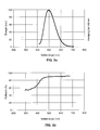
- FIG. 4 shows the emission spectrum (FIG. 4a) of the sialon Ca 1.5 Al 3 Si 9 N 16 : Ce 3+ (5%) (test number HU31 / 01) when excited by 400 nm.
- the maximum is 498 nm, the mean wavelength is 520 nm.
- the quantum efficiency QE is 53%.
- FIG. 5 shows the emission spectrum (FIG. 5a) of the sialon Ca 1.5 Al 3 Si 9 N 16 : Ce 3+ (8%) (test number HU32 / 01) when excited by 400 nm.
- the maximum is 508 nm, the mean wavelength is 523 nm.
- the quantum efficiency QE is 45%.
- FIG. 6 shows the quantum efficiency as a function of the temperature for different phosphors. It shows that the green-emitting thiogallate SrGa 2 S 4 : Eu (curve represented by triangles), which is known per se, has a comparable quantum efficiency (normalized to 100% at room temperature) than a typical sialon (curve represented by diamonds) is represented: here HU18A / 01 from Tab. 1). The value 100% corresponds absolutely to a quantum efficiency of approximately 66%. Surprisingly, the quantum efficiency of the thiogallate deteriorates significantly during operation of the LED under typical temperature loads of 80 ° C to 100 ° C, while the Ce-doped Sialon phosphor maintains its quantum efficiency almost constant.
Abstract
Description
- Figur 1
- ein Halbleiterbauelement, das als Lichtquelle (LED) für weißes Licht dient;
- Figur 2
- eine Beleuchtungseinheit mit Leuchtstoffen gemäß der vorliegenden Erfindung;
- Figur 3 bis 5
- das Emissionsspektrum und Reflexionsspektrum von verschiedenen Sialon-Leuchtstoffen gemäß der vorliegenden Erfindung;
- Figur 6
- das Temperaturverhalten von Sialon HU18A/01 sowie das Temperaturverhalten von Thiogallat-Leuchtstoff im Vergleich.
| Verbindung | Kurzbezeichnung | QE | R360 | R400 | Max. Em. | x | y |
| Ca1.5Al3Si9N16:Ce3+ (2,7%) | HU18A/01 | 66 | 57 | 66 | 499 | 0,220 | 0,396 |
| Ca1.5Al3Si9N16:Ce3+ (5%) | HU31/01 | 53 | 48 | 55 | 498 | 0,237 | 0,422 |
| Ca1.5Al3Si9N16:Ce3+ (8%) | HU32/01 | 45 | 40 | 48 | 508 | 0,247 | 0,435 |
| Ca1.5Al3Si9N16:Ce3+ (2,7%) | HU18/01 | 61 | 55 | 67 | 497 | 0,225 | 0,397 |
Claims (13)
- Beleuchtungseinheit mit mindestens einer LED als Lichtquelle, wobei die LED primäre Strahlung im Bereich 300 bis 430 nm, insbesondere 380 bis 420 nm, emittiert, wobei diese Strahlung vollständig in längerwellige Strahlung konvertiert wird durch Leuchtstoffe, die der primären Strahlung der LED ausgesetzt sind, dadurch gekennzeichnet, dass die Konversion zumindest unter Zuhilfenahme eines Leuchtstoffs erfolgt der grün mit einer Wellenlänge der Peakemission bei 495 bis 540 nm emittiert und der aus der Klasse der Ce-aktivierten Sialone stammt, wobei das Sialon der Formel Mp/2Si12-p-qAlp+qOqN16-q:Ce3+ gehorcht, mit M = Ca einzeln oder in Kombination mit Sr, mit q = 0 bis 2,5 und p = 1,5 bis 3.
- Beleuchtungseinheit nach Anspruch 1, dadurch gekennzeichnet, dass das Ca teilweise (bis zu 30 mol-%) durch Sr ersetzt ist.
- Beleuchtungseinheit nach Anspruch 1, dadurch gekennzeichnet, dass q < 1,insbesondere q ≤ 0,8, und/oder p = 2,5 bis 3 gewählt ist.
- Beleuchtungseinheit nach Anspruch 1, dadurch gekennzeichnet, dass der mittlere Korndurchmesser des grünen Leuchtstoffs zwischen 0,5 und 5 µm beträgt.
- Beleuchtungseinheit nach Anspruch 1, dadurch gekennzeichnet, dass zur Erzeugung von weißem Licht die primär emittierte Strahlung im Wellenlängenbereich 370 bis 420 nm liegt, wobei die primär emittierte Strahlung zumindest drei Leuchtstoffen mit Emissionsmaximum im Blauen (430 bis 470 nm), Grünen (495 bis 540 nm) und Roten (insbesondere 540 bis 620 nm) zur Konversion ausgesetzt ist.
- Beleuchtungseinheit nach Anspruch 5, dadurch gekennzeichnet, dass der weitere rote Leuchtstoff ein Eu-dotiertes Sialon ist.
- Beleuchtungseinheit nach Anspruch 1, dadurch gekennzeichnet, dass zur Erzeugung von farbigem Licht die primär emittierteStrahlung im UV-Wellenlängenbereich von 370 bis 420 nm liegt, wobei die primär emittierte Strahlung einem einzigen Leuchtstoff mit Emissionsmaximum im Grünen (495 nm bis 540 nm) entsprechend einem der vorherigen Ansprüche 1 bis 4 ausgesetzt ist.
- Beleuchtungseinheit nach Anspruch 5, dadurch gekennzeichnet, dass der Mischungsanteil des grünen Leuchtstoffs etwa 0,5 bis 15 % beträgt.
- Beleuchtungseinheit nach Anspruch 1, dadurch gekennzeichnet, dass als primäre Strahlungsquelle eine kurzwellig emittierende Leuchtdiode, insbesondere auf Basis von Ga(In)N, verwendet wird.
- Beleuchtungseinheit nach Anspruch 1, dadurch gekennzeichnet, dass die Beleuchtungseinheit eine Lumineszenzkonversions-LED ist, bei der die Leuchtstoffe direkt oder mittelbar in Kontakt mit dem Chip stehen.
- Beleuchtungseinheit nach Anspruch 1, dadurch gekennzeichnet, dass die Beleuchtungseinheit ein Feld (Array) von LEDs ist.
- Beleuchtungseinheit nach Anspruch 12, dadurch gekennzeichnet, dass zumindest einer der Leuchtstoffe auf einer vor dem LED-Feld angebrachten optischen Vorrichtung angebracht ist.
- Leuchtstoff aus der Klasse der Ce-dotierten Sialone, dadurch gekennzeichnet, dass das Ce-dotierte Sialon der Formel Mp/2Si12-p-qAlp+qOqN16-q:Ce3+ gehorcht, mit M = Ca einzeln oder in Kombination mit Sr, mit q = 0 bis 0,8 und p = 1,5 bis 3.
Applications Claiming Priority (2)
| Application Number | Priority Date | Filing Date | Title |
|---|---|---|---|
| DE10146719 | 2001-09-20 | ||
| DE10146719A DE10146719A1 (de) | 2001-09-20 | 2001-09-20 | Beleuchtungseinheit mit mindestens einer LED als Lichtquelle |
Publications (2)
| Publication Number | Publication Date |
|---|---|
| EP1296383A2 true EP1296383A2 (de) | 2003-03-26 |
| EP1296383A3 EP1296383A3 (de) | 2007-02-28 |
Family
ID=7699894
Family Applications (1)
| Application Number | Title | Priority Date | Filing Date |
|---|---|---|---|
| EP02015876A Withdrawn EP1296383A3 (de) | 2001-09-20 | 2002-07-16 | Beleuchtungseinheit mit mindestens einer LED als Lichtquelle |
Country Status (5)
| Country | Link |
|---|---|
| US (1) | US6674233B2 (de) |
| EP (1) | EP1296383A3 (de) |
| JP (1) | JP2003203504A (de) |
| KR (1) | KR20030025814A (de) |
| DE (1) | DE10146719A1 (de) |
Cited By (15)
| Publication number | Priority date | Publication date | Assignee | Title |
|---|---|---|---|---|
| WO2003107441A2 (en) * | 2002-06-13 | 2003-12-24 | Cree, Inc. | Saturated phosphor solid emitter |
| WO2007041563A2 (en) | 2005-09-30 | 2007-04-12 | The Regents Of The University Of California | Cerium based phosphor materials for solid-state lighting applications |
| EP1867697A1 (de) * | 2005-03-04 | 2007-12-19 | Dowa Mining Co., Ltd. | Fluoreszierende substanz und herstellungsverfahren dafür sowie davon gebrauch machende lichtemittierende vorrichtung |
| EP1878778A1 (de) * | 2005-03-31 | 2008-01-16 | DOWA Electronics Materials Co., Ltd. | Fluoreszenzstoff, fluoreszenzstoffblatt und verfahren zur herstellung dafür sowie auf dem fluoreszenzstoff basierende lumineszenzvorrichtung |
| EP2022836A1 (de) * | 2004-08-27 | 2009-02-11 | DOWA Electronics Materials Co., Ltd. | Phosphor und Herstellungsverfahren dafür, und Lichtquelle dafür |
| US7573190B2 (en) | 2004-02-18 | 2009-08-11 | National Institute For Materials Science | Light emitting element and lighting instrument |
| US7794624B2 (en) | 2002-10-16 | 2010-09-14 | Nichia Corporation | Oxynitride phosphor and production process thereof, and light-emitting device using oxynitride phosphor |
| US7884539B2 (en) | 2004-07-09 | 2011-02-08 | Dowa Electronics Materials Co., Ltd. | Light source having phosphor including divalent, trivalent and tetravalent elements |
| US8066910B2 (en) | 2004-07-28 | 2011-11-29 | Dowa Electronics Materials Co., Ltd. | Phosphor and manufacturing method for the same, and light source |
| US8344611B2 (en) | 2009-06-16 | 2013-01-01 | The Regents Of The University Of California | Oxyfluoride phosphors and white light emitting diodes including the oxyfluoride phosphor for solid-state lighting applications |
| US8409470B2 (en) | 2003-11-26 | 2013-04-02 | Independent Administrative Institution National Institute For Materials Science | Phosphor and light-emitting equipment using phosphor |
| EP2597129A1 (de) * | 2011-11-16 | 2013-05-29 | Kabushiki Kaisha Toshiba | Leuchtstoffmaterial auf der Basis von cerium dotiertem SrSiAlON derivaten |
| US8535565B2 (en) | 2009-10-30 | 2013-09-17 | The Regents Of The University Of California | Solid solution phosphors based on oxyfluoride and white light emitting diodes including the phosphors for solid state white lighting applications |
| EP2778210A1 (de) * | 2013-03-15 | 2014-09-17 | Kabushiki Kaisha Toshiba | Fluoreszente Substanz und lichtemittierende Vorrichtung damit |
| EP2778211A1 (de) * | 2013-03-15 | 2014-09-17 | Kabushiki Kaisha Toshiba | Phosphor und lichtemittierende Vorrichtung damit |
Families Citing this family (89)
| Publication number | Priority date | Publication date | Assignee | Title |
|---|---|---|---|---|
| US6632379B2 (en) * | 2001-06-07 | 2003-10-14 | National Institute For Materials Science | Oxynitride phosphor activated by a rare earth element, and sialon type phosphor |
| JP3726131B2 (ja) * | 2002-05-23 | 2005-12-14 | 独立行政法人物質・材料研究機構 | サイアロン系蛍光体 |
| DE10133352A1 (de) * | 2001-07-16 | 2003-02-06 | Patent Treuhand Ges Fuer Elektrische Gluehlampen Mbh | Beleuchtungseinheit mit mindestens einer LED als Lichtquelle |
| DE10147040A1 (de) * | 2001-09-25 | 2003-04-24 | Patent Treuhand Ges Fuer Elektrische Gluehlampen Mbh | Beleuchtungseinheit mit mindestens einer LED als Lichtquelle |
| JP4207489B2 (ja) * | 2002-08-06 | 2009-01-14 | 株式会社豊田中央研究所 | α−サイアロン蛍光体 |
| US7800121B2 (en) * | 2002-08-30 | 2010-09-21 | Lumination Llc | Light emitting diode component |
| US7224000B2 (en) | 2002-08-30 | 2007-05-29 | Lumination, Llc | Light emitting diode component |
| US20040061810A1 (en) * | 2002-09-27 | 2004-04-01 | Lumileds Lighting, U.S., Llc | Backlight for a color LCD using wavelength-converted light emitting devices |
| JP4442101B2 (ja) * | 2003-03-14 | 2010-03-31 | 日亜化学工業株式会社 | 酸窒化物蛍光体及びそれを用いた発光装置 |
| JP2004210921A (ja) * | 2002-12-27 | 2004-07-29 | Nichia Chem Ind Ltd | オキシ窒化物蛍光体及びその製造方法並びにそれを用いた発光装置 |
| JP4072632B2 (ja) * | 2002-11-29 | 2008-04-09 | 豊田合成株式会社 | 発光装置及び発光方法 |
| AU2003283731A1 (en) * | 2002-12-13 | 2004-07-09 | Koninklijke Philips Electronics N.V. | Illumination system comprising a radiation source and a fluorescent material |
| US20040218387A1 (en) * | 2003-03-18 | 2004-11-04 | Robert Gerlach | LED lighting arrays, fixtures and systems and method for determining human color perception |
| JP2004277663A (ja) * | 2003-03-18 | 2004-10-07 | National Institute For Materials Science | サイアロン蛍光体とその製造方法 |
| US20040207311A1 (en) * | 2003-04-18 | 2004-10-21 | Jung-Pin Cheng | White light emitting device |
| JP4165318B2 (ja) * | 2003-07-16 | 2008-10-15 | 宇部興産株式会社 | サイアロン系蛍光体およびその製造方法 |
| TW200523340A (en) * | 2003-09-24 | 2005-07-16 | Patent Treuhand Ges Fur Elek Sche Gluhlampen Mbh | Hochefeizienter leuchtstoff |
| JP4413570B2 (ja) * | 2003-10-02 | 2010-02-10 | ラボ・スフィア株式会社 | 広角局部照明装置及びバルク型レンズ |
| JP4834827B2 (ja) * | 2003-10-03 | 2011-12-14 | 独立行政法人物質・材料研究機構 | 酸窒化物蛍光体 |
| TWI359187B (en) * | 2003-11-19 | 2012-03-01 | Panasonic Corp | Method for preparing nitridosilicate-based compoun |
| JP4277666B2 (ja) * | 2003-12-01 | 2009-06-10 | 宇部興産株式会社 | サイアロン系蛍光体の製造方法およびサイアロン系蛍光体 |
| US8368092B2 (en) * | 2004-01-26 | 2013-02-05 | Osram Opto Semiconductors Gmbh | Thin film LED comprising a current-dispersing structure |
| TW200525779A (en) * | 2004-01-27 | 2005-08-01 | Super Nova Optoelectronics Corp | White-like light emitting device and its manufacturing method |
| TWI250664B (en) * | 2004-01-30 | 2006-03-01 | South Epitaxy Corp | White light LED |
| JP4976857B2 (ja) * | 2004-02-20 | 2012-07-18 | コーニンクレッカ フィリップス エレクトロニクス エヌ ヴィ | 放射線源および蛍光材料を有する照明システム |
| JP2005285925A (ja) * | 2004-03-29 | 2005-10-13 | Stanley Electric Co Ltd | Led |
| US7488990B2 (en) * | 2004-04-02 | 2009-02-10 | Avago Technologies Ecbu Ip (Singapore) Pte. Ltd. | Using multiple types of phosphor in combination with a light emitting device |
| WO2005103199A1 (en) * | 2004-04-27 | 2005-11-03 | Matsushita Electric Industrial Co., Ltd. | Phosphor composition and method for producing the same, and light-emitting device using the same |
| JP2008503087A (ja) * | 2004-06-18 | 2008-01-31 | コーニンクレッカ フィリップス エレクトロニクス エヌ ヴィ | 改善された光放射率プロファイルを備えるled |
| US7267787B2 (en) * | 2004-08-04 | 2007-09-11 | Intematix Corporation | Phosphor systems for a white light emitting diode (LED) |
| US20060049414A1 (en) * | 2004-08-19 | 2006-03-09 | Chandran Ramachandran G | Novel oxynitride phosphors |
| JP4543250B2 (ja) * | 2004-08-27 | 2010-09-15 | Dowaエレクトロニクス株式会社 | 蛍光体混合物および発光装置 |
| JP4543251B2 (ja) * | 2004-08-31 | 2010-09-15 | Dowaエレクトロニクス株式会社 | 蛍光体及び光源 |
| JP4543253B2 (ja) * | 2004-10-28 | 2010-09-15 | Dowaエレクトロニクス株式会社 | 蛍光体混合物および発光装置 |
| JP2006137902A (ja) * | 2004-11-15 | 2006-06-01 | Shoei Chem Ind Co | 窒化物蛍光体、窒化物蛍光体の製造方法及び白色発光素子 |
| CN102660269B (zh) * | 2005-02-21 | 2014-10-22 | 皇家飞利浦电子股份有限公司 | 包含辐射源和发光材料的照明系统 |
| WO2006093135A1 (ja) * | 2005-02-28 | 2006-09-08 | Denki Kagaku Kogyo Kabushiki Kaisha | 蛍光体とその製造方法、及びそれを用いた発光素子 |
| US7439668B2 (en) * | 2005-03-01 | 2008-10-21 | Lumination Llc | Oxynitride phosphors for use in lighting applications having improved color quality |
| US7524437B2 (en) | 2005-03-04 | 2009-04-28 | Dowa Electronics Materials Co., Ltd. | Phosphor and manufacturing method of the same, and light emitting device using the phosphor |
| WO2006101095A1 (ja) | 2005-03-22 | 2006-09-28 | National Institute For Materials Science | 蛍光体とその製造方法 |
| WO2006101096A1 (ja) * | 2005-03-22 | 2006-09-28 | National Institute For Materials Science | 蛍光体とその製造方法および発光器具 |
| KR101142519B1 (ko) | 2005-03-31 | 2012-05-08 | 서울반도체 주식회사 | 적색 형광체 및 녹색 형광체를 갖는 백색 발광다이오드를채택한 백라이트 패널 |
| WO2006126817A1 (en) | 2005-05-24 | 2006-11-30 | Seoul Semiconductor Co., Ltd. | Green phosphor of thiogallate, red phosphor of alkaline earth sulfide and white light emitting device thereof |
| JP2007049114A (ja) | 2005-05-30 | 2007-02-22 | Sharp Corp | 発光装置とその製造方法 |
| DE102005025416A1 (de) * | 2005-06-02 | 2006-12-14 | Osram Opto Semiconductors Gmbh | Lumineszenzdiodenchip mit einer Kontaktstruktur |
| KR100801938B1 (ko) * | 2005-07-11 | 2008-02-27 | 라이트하우스 테크놀로지 씨오., 엘티디. | 발광 다이오드 패키지 구조 및 그 축광 물질 |
| JP5106761B2 (ja) * | 2005-07-14 | 2012-12-26 | 株式会社フジクラ | 高演色性発光ダイオードランプユニット |
| KR100724591B1 (ko) | 2005-09-30 | 2007-06-04 | 서울반도체 주식회사 | 발광 소자 및 이를 포함한 led 백라이트 |
| US20070145879A1 (en) * | 2005-12-22 | 2007-06-28 | Abramov Vladimir S | Light emitting halogen-silicate photophosphor compositions and systems |
| JP4991027B2 (ja) * | 2005-12-26 | 2012-08-01 | 日亜化学工業株式会社 | オキシ窒化物蛍光体及びそれを用いた発光装置 |
| WO2007105845A1 (en) | 2006-03-16 | 2007-09-20 | Seoul Semiconductor Co., Ltd. | Fluorescent material and light emitting diode using the same |
| JP4805026B2 (ja) * | 2006-05-29 | 2011-11-02 | シャープ株式会社 | 発光装置、表示装置及び発光装置の制御方法 |
| KR101258229B1 (ko) * | 2006-06-30 | 2013-04-25 | 서울반도체 주식회사 | 발광 소자 |
| JP5188687B2 (ja) * | 2006-07-18 | 2013-04-24 | 昭和電工株式会社 | 蛍光体及びその製造法並びに発光装置 |
| US20080029720A1 (en) * | 2006-08-03 | 2008-02-07 | Intematix Corporation | LED lighting arrangement including light emitting phosphor |
| US7842960B2 (en) * | 2006-09-06 | 2010-11-30 | Lumination Llc | Light emitting packages and methods of making same |
| KR101008762B1 (ko) * | 2006-10-12 | 2011-01-14 | 파나소닉 주식회사 | 발광 장치 및 그 제조 방법 |
| DE102006051756A1 (de) | 2006-11-02 | 2008-05-08 | MAX-PLANCK-Gesellschaft zur Förderung der Wissenschaften e.V. | Lichtquelle |
| US20090065715A1 (en) * | 2007-08-24 | 2009-03-12 | Lee Wainright | Universal ultraviolet/ IR/ visible light emitting module |
| CN102036999A (zh) * | 2008-03-21 | 2011-04-27 | 内诺格雷姆公司 | 金属硅氮化物或金属硅氧氮化物亚微米荧光粉颗粒及合成这些荧光粉的方法 |
| JP5002819B2 (ja) * | 2008-06-27 | 2012-08-15 | 独立行政法人物質・材料研究機構 | サイアロン蛍光体およびそれを用いた白色発光ダイオード |
| JP5388699B2 (ja) * | 2009-05-29 | 2014-01-15 | 電気化学工業株式会社 | α型サイアロン蛍光体およびそれを用いた発光素子 |
| US8593040B2 (en) | 2009-10-02 | 2013-11-26 | Ge Lighting Solutions Llc | LED lamp with surface area enhancing fins |
| JP4991834B2 (ja) | 2009-12-17 | 2012-08-01 | シャープ株式会社 | 車両用前照灯 |
| US9631782B2 (en) * | 2010-02-04 | 2017-04-25 | Xicato, Inc. | LED-based rectangular illumination device |
| JP5232815B2 (ja) * | 2010-02-10 | 2013-07-10 | シャープ株式会社 | 車両用前照灯 |
| JP5059208B2 (ja) * | 2010-04-07 | 2012-10-24 | シャープ株式会社 | 照明装置および車両用前照灯 |
| US8733996B2 (en) | 2010-05-17 | 2014-05-27 | Sharp Kabushiki Kaisha | Light emitting device, illuminating device, and vehicle headlamp |
| CN102376860A (zh) * | 2010-08-05 | 2012-03-14 | 夏普株式会社 | 发光装置及其制造方法 |
| JP5185421B2 (ja) * | 2010-09-09 | 2013-04-17 | 株式会社東芝 | 赤色発光蛍光体およびそれを用いた発光装置 |
| US8957585B2 (en) | 2010-10-05 | 2015-02-17 | Intermatix Corporation | Solid-state light emitting devices with photoluminescence wavelength conversion |
| US8614539B2 (en) | 2010-10-05 | 2013-12-24 | Intematix Corporation | Wavelength conversion component with scattering particles |
| US8604678B2 (en) | 2010-10-05 | 2013-12-10 | Intematix Corporation | Wavelength conversion component with a diffusing layer |
| US8610341B2 (en) | 2010-10-05 | 2013-12-17 | Intematix Corporation | Wavelength conversion component |
| US8610340B2 (en) | 2010-10-05 | 2013-12-17 | Intematix Corporation | Solid-state light emitting devices and signage with photoluminescence wavelength conversion |
| US9546765B2 (en) | 2010-10-05 | 2017-01-17 | Intematix Corporation | Diffuser component having scattering particles |
| US9816677B2 (en) | 2010-10-29 | 2017-11-14 | Sharp Kabushiki Kaisha | Light emitting device, vehicle headlamp, illumination device, and laser element |
| JP2012123940A (ja) * | 2010-12-06 | 2012-06-28 | Sharp Corp | 照明装置、及び車両用前照灯 |
| JP5341154B2 (ja) * | 2011-08-31 | 2013-11-13 | 株式会社フジクラ | 高演色性発光ダイオードランプユニット |
| US9500355B2 (en) | 2012-05-04 | 2016-11-22 | GE Lighting Solutions, LLC | Lamp with light emitting elements surrounding active cooling device |
| WO2014026486A1 (zh) * | 2012-08-17 | 2014-02-20 | Qian Zhiqiang | 白光led发光装置 |
| JP5746672B2 (ja) | 2012-09-25 | 2015-07-08 | 株式会社東芝 | 蛍光体、発光装置、および蛍光体の製造方法 |
| EP3176836B1 (de) * | 2012-10-04 | 2024-04-10 | Seoul Semiconductor Co., Ltd. | Weisslichtemittierende vorrichtung, beleuchtungssystem und zahnbeleuchtungssystem |
| US20140185269A1 (en) | 2012-12-28 | 2014-07-03 | Intermatix Corporation | Solid-state lamps utilizing photoluminescence wavelength conversion components |
| CN105121951A (zh) | 2013-03-15 | 2015-12-02 | 英特曼帝克司公司 | 光致发光波长转换组件 |
| DE102013105307A1 (de) | 2013-05-23 | 2014-11-27 | Osram Opto Semiconductors Gmbh | Verfahren zur Herstellung eines pulverförmigen Precursormaterials, pulverförmiges Precursormaterial und seine Verwendung |
| JP6028858B2 (ja) | 2013-05-28 | 2016-11-24 | 宇部興産株式会社 | 酸窒化物蛍光体粉末 |
| JP6187342B2 (ja) * | 2014-03-20 | 2017-08-30 | 宇部興産株式会社 | 酸窒化物蛍光体粉末およびその製造方法 |
| DE102015110258A1 (de) * | 2015-06-25 | 2016-12-29 | Osram Gmbh | Leuchtstoff, Verfahren zum Herstellen eines Leuchtstoffs und Verwendung eines Leuchtstoffs |
Citations (2)
| Publication number | Priority date | Publication date | Assignee | Title |
|---|---|---|---|---|
| US5998925A (en) * | 1996-07-29 | 1999-12-07 | Nichia Kagaku Kogyo Kabushiki Kaisha | Light emitting device having a nitride compound semiconductor and a phosphor containing a garnet fluorescent material |
| WO2001008453A1 (de) * | 1999-07-23 | 2001-02-01 | Osram Opto Semiconductors Gmbh & Co. Ohg | Leuchtstoffanordnung, wellenlängenkonvertierende vergussmasse und lichtquelle |
Family Cites Families (3)
| Publication number | Priority date | Publication date | Assignee | Title |
|---|---|---|---|---|
| AU727132B2 (en) * | 1995-11-01 | 2000-12-07 | Industrial Research Limited | Process for the production of ceramic materials |
| DE19638667C2 (de) | 1996-09-20 | 2001-05-17 | Osram Opto Semiconductors Gmbh | Mischfarbiges Licht abstrahlendes Halbleiterbauelement mit Lumineszenzkonversionselement |
| KR100235203B1 (ko) * | 1997-03-15 | 1999-12-15 | 배문한 | 표면이 개질된 사이알론 복합체 및 그것의 제조 방법 |
-
2001
- 2001-09-20 DE DE10146719A patent/DE10146719A1/de not_active Withdrawn
-
2002
- 2002-07-16 EP EP02015876A patent/EP1296383A3/de not_active Withdrawn
- 2002-07-18 US US10/197,759 patent/US6674233B2/en not_active Expired - Fee Related
- 2002-09-13 KR KR1020020055614A patent/KR20030025814A/ko not_active Application Discontinuation
- 2002-09-19 JP JP2002273458A patent/JP2003203504A/ja active Pending
Patent Citations (2)
| Publication number | Priority date | Publication date | Assignee | Title |
|---|---|---|---|---|
| US5998925A (en) * | 1996-07-29 | 1999-12-07 | Nichia Kagaku Kogyo Kabushiki Kaisha | Light emitting device having a nitride compound semiconductor and a phosphor containing a garnet fluorescent material |
| WO2001008453A1 (de) * | 1999-07-23 | 2001-02-01 | Osram Opto Semiconductors Gmbh & Co. Ohg | Leuchtstoffanordnung, wellenlängenkonvertierende vergussmasse und lichtquelle |
Non-Patent Citations (2)
| Title |
|---|
| KREVEL VAN: "LUMINESCENCE PROPERTIES OF RARE EARTH DOPED ALPHA-SIALON MATERIALS" ON NEW RARE-EARTH DOPED M-SI-AL-O-N MATERIALS, XX, XX, 2000, Seiten 145-157, XP008060386 * |
| MANDAL H; THOMPSON D P: "CeO2-doped alpha-sialon ceramics" JOURNAL OF MATERIALS SCIENCE LETTERS, Bd. 15, 1996, Seiten 1435-1438, XP008074097 * |
Cited By (34)
| Publication number | Priority date | Publication date | Assignee | Title |
|---|---|---|---|---|
| MY138406A (en) * | 2002-06-13 | 2009-05-29 | Cree Inc | Saturated phosphor solid state emitter |
| WO2003107441A3 (en) * | 2002-06-13 | 2004-07-15 | Cree Inc | SOLID STATE PHOSPHORUS TRANSMITTER |
| WO2003107441A2 (en) * | 2002-06-13 | 2003-12-24 | Cree, Inc. | Saturated phosphor solid emitter |
| US7951307B2 (en) | 2002-10-16 | 2011-05-31 | Nichia Corporation | Oxynitride phosphor and production process thereof, and light-emitting device using oxynitride phosphor |
| US7951306B2 (en) | 2002-10-16 | 2011-05-31 | Nichia Corporation | Oxynitride phosphor and production process thereof, and light-emitting device using oxynitride phosphor |
| US7794624B2 (en) | 2002-10-16 | 2010-09-14 | Nichia Corporation | Oxynitride phosphor and production process thereof, and light-emitting device using oxynitride phosphor |
| US7951308B2 (en) | 2002-10-16 | 2011-05-31 | Nichia Corporation | Oxynitride phosphor and production process thereof, and light-emitting device using oxynitride phosphor |
| US8409470B2 (en) | 2003-11-26 | 2013-04-02 | Independent Administrative Institution National Institute For Materials Science | Phosphor and light-emitting equipment using phosphor |
| US9738829B2 (en) | 2003-11-26 | 2017-08-22 | Mitsubishi Chemical Corporation | Phosphor and light-emitting equipment using phosphor |
| US10072207B2 (en) | 2003-11-26 | 2018-09-11 | Mitsubishi Chemical Corporation | Phosphor and light-emitting equipment using phosphor |
| US11084980B2 (en) | 2003-11-26 | 2021-08-10 | Mitsubishi Chemical Corporation | Phosphor and light-emitting equipment using phosphor |
| US11697765B2 (en) | 2003-11-26 | 2023-07-11 | Mitsubishi Chemical Corporation | Phosphor and light-emitting equipment using phosphor |
| US7573190B2 (en) | 2004-02-18 | 2009-08-11 | National Institute For Materials Science | Light emitting element and lighting instrument |
| US8441180B2 (en) | 2004-07-09 | 2013-05-14 | Dowa Electronics Materials Co., Ltd. | Light source having phosphor including divalent, trivalent and tetravalent elements |
| US7884539B2 (en) | 2004-07-09 | 2011-02-08 | Dowa Electronics Materials Co., Ltd. | Light source having phosphor including divalent, trivalent and tetravalent elements |
| US8066910B2 (en) | 2004-07-28 | 2011-11-29 | Dowa Electronics Materials Co., Ltd. | Phosphor and manufacturing method for the same, and light source |
| US8308981B2 (en) * | 2004-08-27 | 2012-11-13 | Dowa Electronics Materials Co., Ltd. | Phosphor and manufacturing method for the same, and light source |
| US7803286B2 (en) | 2004-08-27 | 2010-09-28 | Dowa Electronics Materials Co., Ltd. | Phosphor and manufacturing method for the same, and light source |
| EP2022836A1 (de) * | 2004-08-27 | 2009-02-11 | DOWA Electronics Materials Co., Ltd. | Phosphor und Herstellungsverfahren dafür, und Lichtquelle dafür |
| US8372309B2 (en) | 2005-02-25 | 2013-02-12 | Mitsubishi Chemical Corporation | Phosphor and manufacturing method therefore, and light emission device using the phosphor |
| EP1867697A4 (de) * | 2005-03-04 | 2012-03-21 | Mitsubishi Chem Corp | Fluoreszierende substanz und herstellungsverfahren dafür sowie davon gebrauch machende lichtemittierende vorrichtung |
| EP1867697A1 (de) * | 2005-03-04 | 2007-12-19 | Dowa Mining Co., Ltd. | Fluoreszierende substanz und herstellungsverfahren dafür sowie davon gebrauch machende lichtemittierende vorrichtung |
| EP1878778A4 (de) * | 2005-03-31 | 2012-04-04 | Mitsubishi Chem Corp | Fluoreszenzstoff, fluoreszenzstoffblatt und verfahren zur herstellung dafür sowie auf dem fluoreszenzstoff basierende lumineszenzvorrichtung |
| EP1878778A1 (de) * | 2005-03-31 | 2008-01-16 | DOWA Electronics Materials Co., Ltd. | Fluoreszenzstoff, fluoreszenzstoffblatt und verfahren zur herstellung dafür sowie auf dem fluoreszenzstoff basierende lumineszenzvorrichtung |
| US8920676B2 (en) | 2005-09-30 | 2014-12-30 | The Regents Of The University Of California | Cerium based phosphor materials for solid-state lighting applications |
| EP1929502A4 (de) * | 2005-09-30 | 2010-03-24 | Univ California | Auf cer basierende leuchtstoffmatierialien für halbleiter-beleuchtungsanwendungen |
| WO2007041563A2 (en) | 2005-09-30 | 2007-04-12 | The Regents Of The University Of California | Cerium based phosphor materials for solid-state lighting applications |
| EP1929502A2 (de) * | 2005-09-30 | 2008-06-11 | The Regents of the University of California | Auf cer basierende leuchtstoffmatierialien für halbleiter-beleuchtungsanwendungen |
| US8344611B2 (en) | 2009-06-16 | 2013-01-01 | The Regents Of The University Of California | Oxyfluoride phosphors and white light emitting diodes including the oxyfluoride phosphor for solid-state lighting applications |
| US8535565B2 (en) | 2009-10-30 | 2013-09-17 | The Regents Of The University Of California | Solid solution phosphors based on oxyfluoride and white light emitting diodes including the phosphors for solid state white lighting applications |
| US9133391B2 (en) | 2011-11-16 | 2015-09-15 | Kabushiki Kaisha Toshiba | Luminescent material |
| EP2597129A1 (de) * | 2011-11-16 | 2013-05-29 | Kabushiki Kaisha Toshiba | Leuchtstoffmaterial auf der Basis von cerium dotiertem SrSiAlON derivaten |
| EP2778211A1 (de) * | 2013-03-15 | 2014-09-17 | Kabushiki Kaisha Toshiba | Phosphor und lichtemittierende Vorrichtung damit |
| EP2778210A1 (de) * | 2013-03-15 | 2014-09-17 | Kabushiki Kaisha Toshiba | Fluoreszente Substanz und lichtemittierende Vorrichtung damit |
Also Published As
| Publication number | Publication date |
|---|---|
| US20030052595A1 (en) | 2003-03-20 |
| KR20030025814A (ko) | 2003-03-29 |
| US6674233B2 (en) | 2004-01-06 |
| EP1296383A3 (de) | 2007-02-28 |
| DE10146719A1 (de) | 2003-04-17 |
| JP2003203504A (ja) | 2003-07-18 |
Similar Documents
| Publication | Publication Date | Title |
|---|---|---|
| EP1296383A2 (de) | Beleuchtungseinheit mit mindestens einer LED als Lichtquelle | |
| EP1278250B1 (de) | Beleuchtungseinheit mit mindestens einer LED als Lichtquelle | |
| EP1296376B1 (de) | Beleuchtungseinheit mit mindestens einer LED als Lichtquelle | |
| EP1206802B1 (de) | Weiss emittierende beleuchtungseinheit auf led-basis | |
| DE60307415T2 (de) | Fotolumineszierende stoffe für leuchtdioden, und leuchtdiode | |
| DE10105800B4 (de) | Hocheffizienter Leuchtstoff und dessen Verwendung | |
| DE60307411T2 (de) | Fotolumineszentes material und leuchtdiode | |
| EP1471775B9 (de) | Lichtquelle mit einer Leuchtstoffanordnung und Vergussmasse mit einer Leuchtstoffanordnung | |
| DE60038668T2 (de) | Lichtquelle mit gelben bis roten emittierenden leuchtstoff | |
| DE102006007799B4 (de) | Licht emittierendes Halbleiterbauteil | |
| EP2313473B1 (de) | Alpha-sialon-leuchtstoff | |
| DE10241140A1 (de) | Beleuchtungseinheit mit mindestens einer LED als Lichtquelle | |
| DE112007001638B4 (de) | Leuchtstoff aus der Klasse der Nitridosilikate, Verfahren zur Herstellung eines Leuchtstoff aus der Klasse der Nitridosilikate und Verwendung eines derartigen Leuchtstoffs in einer Lichtquelle | |
| WO2001093341A1 (de) | Weiss emittierende beleuchtungseinheit auf led-basis | |
| EP1966345B1 (de) | Rot emittierender leuchtstoff und lichtquelle mit einem derartigen leuchtstoff | |
| DE102005005263A1 (de) | Gelb emittierender Leuchtstoff und Lichtquelle mit derartigem Leuchtstoff | |
| DE112011100522T5 (de) | Fluoreszierende Substanz, lichtemittierende Vorrichtung, Oberflächenlichtquellenvorrichtung, Anzeigevorrichtung und Beleuchtungsvorrichtung | |
| DE102006016548A1 (de) | Blau bis Gelb-Orange emittierender Leuchtstoff und Lichtquelle mit derartigem Leuchtstoff | |
| EP1670876A1 (de) | Hocheffizienter leuchtstoff | |
| DE102004060708B4 (de) | Rotes Fluoreszenzmaterial und Weißlicht emittierende Dioden, die rotes Fluoreszenzmaterial verwenden | |
| EP2217678B1 (de) | Leuchtstoff und beleuchtungssystem mit derartigem leuchtstoff | |
| DE20122557U1 (de) | Beleuchtungseinheit mit mindestens einer LED als Lichtquelle |
Legal Events
| Date | Code | Title | Description |
|---|---|---|---|
| PUAI | Public reference made under article 153(3) epc to a published international application that has entered the european phase |
Free format text: ORIGINAL CODE: 0009012 |
|
| AK | Designated contracting states |
Kind code of ref document: A2 Designated state(s): AT BE BG CH CY CZ DE DK EE ES FI FR GB GR IE IT LI LU MC NL PT SE SK TR Designated state(s): AT BE BG CH CY CZ DE DK EE ES FI FR GB GR IE IT LI LU MC NL PT SE SK TR |
|
| AX | Request for extension of the european patent |
Extension state: AL LT LV MK RO SI |
|
| PUAL | Search report despatched |
Free format text: ORIGINAL CODE: 0009013 |
|
| AK | Designated contracting states |
Kind code of ref document: A3 Designated state(s): AT BE BG CH CY CZ DE DK EE ES FI FR GB GR IE IT LI LU MC NL PT SE SK TR |
|
| AX | Request for extension of the european patent |
Extension state: AL LT LV MK RO SI |
|
| RIC1 | Information provided on ipc code assigned before grant |
Ipc: C09K 11/08 20060101ALI20070125BHEP Ipc: C09K 11/77 20060101ALI20070125BHEP Ipc: H01L 33/00 20060101AFI20021125BHEP |
|
| AKX | Designation fees paid | ||
| 17P | Request for examination filed |
Effective date: 20070910 |
|
| RBV | Designated contracting states (corrected) |
Designated state(s): BE DE GB NL |
|
| R17P | Request for examination filed (corrected) |
Effective date: 20070910 |
|
| 17Q | First examination report despatched |
Effective date: 20080717 |
|
| D18D | Application deemed to be withdrawn (deleted) | ||
| STAA | Information on the status of an ep patent application or granted ep patent |
Free format text: STATUS: THE APPLICATION IS DEEMED TO BE WITHDRAWN |
|
| 18D | Application deemed to be withdrawn |
Effective date: 20081128 |