EP1316110B1 - Electrostatic chuck with porous regions - Google Patents
Electrostatic chuck with porous regions Download PDFInfo
- Publication number
- EP1316110B1 EP1316110B1 EP01955029A EP01955029A EP1316110B1 EP 1316110 B1 EP1316110 B1 EP 1316110B1 EP 01955029 A EP01955029 A EP 01955029A EP 01955029 A EP01955029 A EP 01955029A EP 1316110 B1 EP1316110 B1 EP 1316110B1
- Authority
- EP
- European Patent Office
- Prior art keywords
- electrostatic chuck
- porous
- green
- chuck
- regions
- Prior art date
- Legal status (The legal status is an assumption and is not a legal conclusion. Google has not performed a legal analysis and makes no representation as to the accuracy of the status listed.)
- Expired - Lifetime
Links
Images
Classifications
-
- H—ELECTRICITY
- H01—ELECTRIC ELEMENTS
- H01L—SEMICONDUCTOR DEVICES NOT COVERED BY CLASS H10
- H01L21/00—Processes or apparatus adapted for the manufacture or treatment of semiconductor or solid state devices or of parts thereof
- H01L21/67—Apparatus specially adapted for handling semiconductor or electric solid state devices during manufacture or treatment thereof; Apparatus specially adapted for handling wafers during manufacture or treatment of semiconductor or electric solid state devices or components ; Apparatus not specifically provided for elsewhere
- H01L21/68—Apparatus specially adapted for handling semiconductor or electric solid state devices during manufacture or treatment thereof; Apparatus specially adapted for handling wafers during manufacture or treatment of semiconductor or electric solid state devices or components ; Apparatus not specifically provided for elsewhere for positioning, orientation or alignment
-
- H—ELECTRICITY
- H01—ELECTRIC ELEMENTS
- H01L—SEMICONDUCTOR DEVICES NOT COVERED BY CLASS H10
- H01L21/00—Processes or apparatus adapted for the manufacture or treatment of semiconductor or solid state devices or of parts thereof
- H01L21/67—Apparatus specially adapted for handling semiconductor or electric solid state devices during manufacture or treatment thereof; Apparatus specially adapted for handling wafers during manufacture or treatment of semiconductor or electric solid state devices or components ; Apparatus not specifically provided for elsewhere
- H01L21/683—Apparatus specially adapted for handling semiconductor or electric solid state devices during manufacture or treatment thereof; Apparatus specially adapted for handling wafers during manufacture or treatment of semiconductor or electric solid state devices or components ; Apparatus not specifically provided for elsewhere for supporting or gripping
- H01L21/6831—Apparatus specially adapted for handling semiconductor or electric solid state devices during manufacture or treatment thereof; Apparatus specially adapted for handling wafers during manufacture or treatment of semiconductor or electric solid state devices or components ; Apparatus not specifically provided for elsewhere for supporting or gripping using electrostatic chucks
- H01L21/6833—Details of electrostatic chucks
Definitions
- Wafer manufacturing frequently requires accurate control of the wafer temperature.
- heat is removed from the wafer, typically by a heat transfer gas.
- the heat transfer gas employed is helium.
- the wafer is mechanically clamped from the periphery of its top surface and helium pressure is supplied from the bottom side of the wafer. This technique can result in wafer non-uniformities and bowing.
- electrostatic wafer holding Both coulombic and Johnson-Rahbek types of electrostatic chucks can be employed during processing to secure a wafer or another workpiece, such as, for example, flat panel displays, onto a chucking surface.
- Some of the available electrostatic chuck designs include an electrode and an insulating or semiconducting layer of material between the electrode and the chucking surface and through-holes for passing helium gas from the back surface to the chucking surface.
- a heat transfer fluid pathway is provided in a conductive chuck pedestal, typically fabricated from aluminum metal and overlaid by a dielectric layer, typically formed by spray-coating a ceramic material such as alumina or alumina/titania.
- the pathway can include a porous dielectric insert which can isolate the conductive pedestal from the pathway. While this design addresses problems relating to arcing and breakdown of helium in a RF plasma environment, it utilizes mechanical means of securing the insert within the pathway. For example, the insert can be held in a dielectric sleeve or secured within the pathway by a press or interference fit. Careful machining is required to provide this fit.
- An electrostatic chuck is for instance described in WO 99/65136 , which comprises a laminated structure having a grain-attracting electrode, a dielectric layer and a shield electrode. Electrostatic chuck holes are formed in the electrostatic chuck. This electrostatic chuck is held on the surface of a vacuum chuck comprising a porous disc. Another electrostatic chuck is described in US 5 542 559 which rests on an electrode having a conduit which includes a porous flow path member.
- EP 0 791 956 describes an electrostatic chuck which comprises an insulating dielectric layer made of a ceramic material having a porosity of less than 3 %.
- An electrostatic chuck is also described in US 5 904 776 which comprises a chuck body and an electrode disposed therein.
- An annular conduit is formed on the chucking surface by a conductive insert fitted into openings created by annular channels.
- the conductive insert which forms the pedestal of the chuck, includes gas passages which are filled with porous dielectric insert.
- the present invention is related to an electrostatic chuck and to a method of fabricating an electrostatic chuck.
- the electrostatic chuck of the invention includes a chuck body having a back surface and a chucking surface.
- the electrostatic chuck also includes an electrode within said chuck body.
- the electrostatic chuck further includes a plurality of conduits for providing fluid communication between the back surface and the chucking surface.
- the conduits include a porous region which is an integral part of the chuck body.
- the chuck body is a ceramic body.
- the porous region has a chemical composition which is essentially the same as the chemical composition of the ceramic body.
- the porous region extends from the back surface to the chucking surface.
- One method of fabricating an electrostatic chuck includes forming a green body of an electrostatic chuck body.
- the green body has at least one region which includes removable particles.
- the method further includes heating the green body to form the electrostatic chuck body and removing the particles, thereby forming a porous region in the electrostatic chuck body.
- the particles can be removed, for example, by heating or by treatment with a decomposing chemical agent.
- Another method of fabricating an electrostatic chuck includes forming in a green body of an electrostatic chuck body at least one green region which, following densification of the green body, will be porous. The method also includes densifying the green body, thereby forming the ceramic electrostatic chuck body which includes at least one porous region.
- the green region includes a sintering aid.
- the green region includes a polymeric component which during densification of the green body decomposes thereby leaving pores and forming the porous region of the electrostatic chuck body.
- the electrode of the electrostatic chuck of the invention is within the chuck body and thus well isolated from the plasma environment.
- the porous region within the conduit for directing a heat transfer fluid to the chucking surface minimizes plasma penetration into the conduit and possible plasma extinguishing.
- the porous region also provides interconnecting channels and pores which are not in a straight line path thereby minimizing arcing problems.
- heat transfer fluid can flow through the pores and channels in enough volume to affect the temperature of the work-piece supported onto the electrostatic chuck.
- the porous region is not held in place by mechanical means such as a sleeve or through an interference or press fitting, which require careful machining, but is an integral part of the chuck body.
- the invention also provides simple methods of manufacturing the electrostatic chuck of the invention.
- the invention relates to an electrostatic chuck and to methods of fabricating an electrostatic chuck.
- Electrostatic chuck 10 can be, for example, of Coulombic type or of Johnson-Rahbek type, with the latter being preferred.
- Electrostatic chuck 10 includes chuck body 12 and, within chuck body 12, electrode 14.
- Electrode 14 can be a foil, a plate, a perforated foil or a perforated plate, a mesh, a screen printed layer or can have some other configuration that is suitable for incorporation into electrostatic chucks. Electrode 14 can be used as a chucking electrode, a plasma generating electrode or both. If the electrode operates as a chucking electrode only, a preferred thickness of the electrode is in a range of between about 10 ⁇ m (micrometers or microns) and about 50 ⁇ m Generally, a plasma generating electrode is thick enough to withstand the radio frequency (RF) applied to it. The preferred thickness of a plasma generating electrode ranges from about 50 ⁇ m to about 1 mm (millimeters).
- RF radio frequency
- a suitable of a mesh electrode has a wire diameter of about 125 ⁇ m and a mesh spacing of 19.6 wires per cm (50 wires per inch).
- electrode 14 is a flat film electrode such as described in U.S. Provisional Patent Application 60/169,859 , Electrostatic Chucks with Flat Film Electrode, filed December 9, 1999. Monoplolar as well as bipolar electrode configurations, as known in the art, can be employed.
- Electrode 14 is fabricated from a suitable metal or from a combination of metals or alloy.
- electrode 14 includes molybdenum (Mo), tungsten (W) or combinations of molybdenum and tungsten.
- Mo, W or Mo-W electrode includes additional metals, such as nickel and cobalt or other components such as sintering activators.
- suitable metals for fabricating of electrode 14 include, but are not limited to, tantalum, platinum, hafnium, rhodium, vanadium and alloys thereof.
- the electrode material is graphite.
- Chuck body 12 includes dielectric layer 16, at upper side 18 of electrode 14, and substrate 20, at lower side 22 of electrode 14.
- electrode 14 is completely and integrally embedded within chuck body 12.
- electrode 14 is sandwiched between dielectric layer 16 and substrate 20.
- a joint or seam (not shown) binds dielectric layer 16 to substrate 20.
- a joint or seam that does not allow ambient atmosphere to interact with electrode 14 is preferred.
- the joint or seam is formed by employing a suitable brazing material.
- the brazing material employed to form the join or seam also functions as electrode 14. Alternatively, there is no joint or seam between dielectric layer 16 and substrate 20.
- the thickness of dielectric layer 16 ranges from about 10 ⁇ m to about 5mm. In another embodiment, the dielectric resistivity of dielectric layer 16 is greater than 10 13 ohm•cm, at the operating temperature of the chuck, which is particularly suitable in the case of a Coulombic-type chuck. In yet another embodiment, the dielectric resistivity of dielectric layer 16 ranges from about 10 8 to about 10 13 ohm•cm, at the operating temperature of the chuck, which is particularly suitable for a Johnson-Rahbek-type electrostatic chuck.
- dielectric layer 16 and/or substrate 20 include but are not limited to aluminum oxide (Al 2 O 3 ), aluminum oxide-titanium oxide (Al 2 O 3 -TiO 2 ), aluminum nitride (AlN), silicon nitride (Si 3 N 4 ), silicon carbide (SiC), boron nitride (BN), yttrium oxide or yttria (Y 2 O 3) , yttrium aluminate (for example, Y 3 Al 5 O 12 , YAlO 3 , Al 2 Y 4 O 9 ) and any combination thereof. AlN is preferred.
- chuck body 12 has an uniform chemical composition.
- chuck body 12 can be constructed from different materials; for example, the chemical composition of substrate 20 can differ from that of dielectric layer 16.
- Chuck body 12, dielectric layer 16 and/or substrate 20 also can include additional components, for example, sintering aids, bonding agents and other materials, known in the art.
- additional components include but are not limited to yttrium oxide (Y 2 O 3 ), calcium salts and oxides, for instance, calcium fluoride or CaF 2 , calcium chloride or CaCl 2 , calcium oxide or CaO, calcium carbonate or CaCO 3 , calcium nitrate or Ca(NO 3 ) 2 , chromium oxide (Cr 2 O 3 ), silica (SiO 2 ), boron nitride (BN) and any combination(s) thereof, as well as secondary phases, formed by reaction(s) between the ceramic material and the additional component(s), such as, for example, compounds including yttrium aluminum and oxygen, for example, Y 3 Al 5 O 12 , YAlO 3 , Al 2 Y 4 O 9 or combinations thereof.
- Y 2 O 3 yttrium oxide
- CaF 2 calcium
- dielectric layer 16 and/or substrate 20 can also include Al 2 O 3 , an oxynitride of aluminum, (for example AlON), Y 2 O 3 , CaF 2 CaCl 2 , CaO, CaCO 3 , Ca(NO 3 ) 2 , Cr 2 O 3 , SiO 2 , BN, Y 3 Al 5 O 12 , YAlO 3 , Al 2 Y 4 O 9 or combinations thereof.
- electrostatic chuck 10 can further include a heating element (not shown).
- a heating element not shown.
- One suitable arrangement of an electrostatic chuck which includes an embedded heating element is described in U.S. Patent Application 09/457,968 , Electrostatic Chuck, Susceptor and Method for Fabrication , filed on December 9, 1999,.
- Electrostatic chuck 10 has back surface 24 and chucking surface 26.
- chucking surface 26 includes protrusions 28 and channels 30.
- a surface pattern such as one including, for example, protruding dimples or ridges significantly reduces contact area between work-piece 32 and chucking surface 26, and allows heat transfer fluid to circulate beneath work-piece 32.
- chucking surface 26 can be coated, for example, for enhanced erosion and/or corrosion resistance.
- Coatings which can be applied onto chucking surface 26 include but are not limited to pyrolytic BN, yttria, an yttrium aluminate, aluminum trfluoride (AlF 3 ), diamond and diamond-like coatings, such as, for example, coatings applied by chemical vapor deposition (CVD) methods. Thin coatings are preferred, such as, for example, coatings ranging from about 1 micrometer ( ⁇ m) to about 100 ⁇ m in thickness.
- electrical connector 34 is attached to electrode 14 through means known in the art.
- electrical connector 34 can be brazed to electrode 14.
- a contact plug (not shown) is co-sintered to the electrode and joined to electrical connector 34. Contacts and/or electrical connectors that have good electrical conductivity, low RF impedence and are easily joined to electrode 14 are preferred.
- electrical connector 34 includes, at electrode 14, an electrical contact such as described in U.S. Patent Application 09/457,968 , Electrostatic Chuck Susceptor and Method for Fabrication , filed on December 9,1999 .
- Electrostatic chuck 10 also includes one or more lift pin holes 36 which accommodate lift pins typically employed to raise or lower work-piece 32 from chucking surface 26.
- lift pin holes 36 extend from back surface 24, through substrate 20, electrode 14, dielectric layer 16, to chucking surface 26.
- Electrode 14 has apertures which align with lift pin holes 36 but, preferably, are larger in diameter, thereby preventing the lift pins from contacting electrode 14.
- the number of lift pin holes 36 generally depends on the chuck design and its application.
- Electrostatic chuck 10 includes at least one conduit 38 which provides fluid communication between back surface 24 and chucking surface 26.
- conduit 38 extends from back surface 24, through substrate 20, electrode 14, dielectric layer 16, to chucking surface 26.
- electrode 14 has apertures which align with conduit 38 and, preferably, are larger in diameter, thereby preventing heat transfer gas flowing through conduit 38 from contacting electrode 14.
- the cross section of conduit 38 can have, for example, a circular, elliptical, ring-like shape or any other suitable shape.
- Either or both the shape or dimensions of the cross section of conduit 38 can be essentially constant throughout the thickness of electrostatic chuck 10. Alternatively, either or both the shape or dimensions of conduit 38 can vary between back surface 24 and chucking surface 26.
- Conduit 38 includes porous zone or region 40 which is integrated within chuck body 12.
- Porous region 40 can include a ceramic material such as, for example, AlN, Si 3 N 4 , Al 2 O 3 , Al 2 O 3 -TiO 2 , SiC.
- porous region 40 can further include one or more components such as, for example, additives, sintering aids or bonding agents.
- additional components include but are not limited to yttrium oxide (Y 2 O 3 ), calcium salts and oxides, for instance, calcium fluoride or CaF 2 , calcium chloride or CaCl 2 , calcium oxide or CaO, calcium carbonate or CaCO 3 , calcium nitrate or Ca(NO 3 ) 2 , chromium oxide (Cr 2 O 3 ), silica (SiO 2 ), boron nitride (BN) and any combination(s) thereof.
- Porous region 40 also can include reaction products, also referred to herein as secondary phases, formed by reaction(s) between the ceramic material and the additional component(s).
- porous region 40 includes AlN and an yttrium aluminate, such as, for example, Y 3 Al 5 O 12 , YAlO 3 , Al 2 Y 4 O 9 or combinations thereof. Porous region 40 can also include Al 2 O 3 or an oxynitride of aluminum, for example AlON. In another embodiment, porous region 40 includes AlN and Y 2 O 3 , CaF 2 , CaCl 2 , CaO, CaCO 3 , Ca(NO 3 ) 2 , Cr 2 O 3 , SiO 2 , BN or a combination(s) thereof. Porous region 40 can be fabricated from the same material employed to fabricate dielectric layer 16 or chuck body 12.
- porous region 40 has a porosity sufficient to allow a required gas flow to the chucking surface. Pores small enough to restrict plasma penetration into conduit 38 are preferred. Also preferred are pores which do not form a direct line of sight between the backside (side resting on electrostatic chuck 10) of workpiece 32, electrode 14 and cathode pedestal 42, which supports electrostatic chuck 10.
- the porosity and average pore size employed can vary depending on the chuck design and/or application of a particular chuck.
- the porosity of porous region 40 is in a range of between about 10% and about 60% and preferably in a range of between about 30% and about 50%.
- average pore size ranges from about 5 ⁇ m to about 500 ⁇ m, with preferred pores having an average size between from about 20 ⁇ m to about 100 ⁇ m.
- Porous region 40 is integrated or integrally bonded to chuck body 12.
- the terms "integrated” or “integrally bonded” mean that porous region 40 is part of chuck body 12.
- the interface between porous region 40 and chuck body 12 does not present cracks, seams, joints or other defects.
- porous region 40 is diffusion-bonded to surrounding chuck body 12.
- porous region 40 is chemically bonded to surrounding chuck body 12.
- Porous region 40 can also be sintered into surrounding chuck body 12.
- a plurality of conduits 38 which include porous region 40, are employed.
- the number, dimensions and arrangement of porous regions 40 can depend, for example, upon the design and/or application of a particular chuck. Porous regions 40 can but need not have the same porosity.
- most or all of chuck body 12 is porous.
- most or all of dielectric layer 16 is porous.
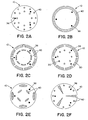
- all porous regions 40 have the same shape. In another embodiment all porous regions 40 have the same dimensions. In still another embodiment electrostatic chuck 10 includes porous regions having different shapes. Some suitable cross sectional shapes of porous region 40 are shown in Figure 3 .
- porous region 40 is a porous plug, such as, for example, a cylindrical porous plug.
- the number, dimensions and arrangement of the porous plugs can depend, for example, upon the design and/or application of a particular chuck.
- the diameter of the porous plug ranges from about 0.5 millimeter (mm) to about 20 mm.
- electrostatic chuck 10 has between about 1 and about 100 porous plugs, and preferably between about 20 and about 50 porous plugs.
- electrostatic chuck 10 includes porous regions 40 which are concentric rings.
- the surface area at the chucking surface of one ring is greater than the surface area of another ring.
- the porosity of the ring having the greater surface area is less than that of the ring which has the smaller surface area.
- porous region 40 prevents the formation of a direct line of sight from workpiece 32 (in particular from the side of workpiece 32 which rests on electrostatic chuck 10) to electrode 14 and to cathode pedestal 42.
- porous region 40 integrally bonded to chuck body 12, extends from back surface 24 to chucking surface 26, as shown in Figure 1 .
- porous region 40 also integrally bonded to chuck body 12, only partially extends through conduit 38.
- FIG. 3A is a cross sectional view of one embodiment of the invention, - represented as electrostatic chuck 44.
- Electrostatic chuck 44 includes conduit 38 to provide fluid communication between back surface 24, and chucking surface 26.
- Conduit 38 includes porous region 40, at back surface 24. Porous region 40 is in the shape of a porous plug and is integrally bonded to substrate 20. Porous region 40 partially extends from back surface 24 through conduit 38, towards, but not all the way to, chucking surface 26.
- Conduit 38 also includes opening 46, which does not include porous material and which extends from porous zone 40 to chucking surface 26. Porosity and other pore-related properties, the numbers and volume of porous regions 40, the diameter and number of openings 46 are factors which can vary from one chuck design to another, depending on the application and the desired volume flow of heat transfer fluid.
- Electrostatic chuck 48 includes porous region 40 at back surface 24. Porous region 40 is integrally bonded to substrate 20. It partially extends from back surface 24, some distance towards, but not all the way to, chucking surface 26.
- the cross section of porous region 40 can be, for example, elliptical, a ring or another suitable shape, such as a shape illustrated in Figure 2 .
- Electrostatic chuck 48 also includes openings 46, which do not include porous material and extend from porous region 40 to chucking surface 26. As discussed above, porosity and other pore-related properties, numbers and volume of porous regions 40, the diameter and number of openings 46 are factors which can vary from one chuck design to another, depending on the application and the desired volume flow of heat transfer fluid.
- the porous region is at the chucking surface and is integrally bonded to the dielectric layer of the chuck body.
- the porous region extends from the chucking surface through the chuck body towards, but not all the way to, the back surface.
- the porous region extends from the chucking surface through the electrode.
- One or more openings for directing heat transfer fluid extend from the porous region to the back surface.
- Porous regions which partially extend through the conduit between the back surface and the chucking surface and are integrally bonded to the chuck body can be placed in other zones within the conduit, for example, away from both the back surface and the chucking surface.
- Electrostatic chucks which combine porous regions which extend from back surface to the chucking surface and porous regions which only partially extend through the conduit also can be fabricated.
- a heat transfer fluid is directed, from back surface 24, through porous region 40 to chucking surface 26.
- a heat transfer fluid is directed from back surface 24, through porous region(s) 40, openings 46 to chucking surface 26.
- Heat transfer fluid exits at chucking surface 26 and, optionally, circulates though channels 22, thereby modifying the temperature of work-piece 32.
- Heat transfer fluid can be supplied from a source, not shown in the figures and directed to porous region 40, for example, through an opening in cathode pedestal 42. Heat transfer fluid can be supplied to porous region 40 via tubings, pipings, regulators, fittings, valves, plenum reservoir(s), any combinations thereof, or other suitable means known in the art.
- heat transfer fluids include, but are not limited to, helium, argon, or other inert gases, as well as gases which are inert in the particular operation, environment and conditions in which electrostatic chuck is employed, and mixtures thereof.
- the heat transfer fluid can be at a temperature suitable in effecting the desired modification of the work-piece temperature.
- Heat transfer fluid within a desired temperature range can be supplied to chuck 10 as known in the art, for example by heating of cooling the heat transfer fluid in a heat exchanger, or by using cryogenic fluids.
- the pressure of heat transfer fluid supplied to conduit 38 can be controlled as known in the art.
- the heat transfer fluid is supplied at a pressure such that the flow of heat transfer fluid exiting at chucking surface 26 does not interfere with the electrostatic forces exerted upon work-piece 32 and the operation of the electrostatic chuck.
- design parameters such as, for example, the porosity, pore size and volume of the porous regions can be chosen to obtain a desired volume flow.
- a desired gas conductance is dependent on the size of pores and the amount of porosity in porous region 40.
- Gas conductance is the volume of gas allowed to flow through at a given pressure.
- the porosity of a large porous region can be adjusted, for example, to yield an equivalent gas conductance of a small porous plug.
- the invention also is related to methods of producing an electrostatic chuck.
- first portion 50 of a green chuck body includes recess 52.
- green refers to the pre-densified state of a ceramic precursor.
- the green chuck body can be a compacted (for example cold-pressed), non-densified body of a precursor, such as, for example a powder or slurry, which upon densification will form a ceramic body.
- first portion 50 is formed by compacting AlN powder.
- Suitable materials which can be employed include, but are not limited to, AlN, Si 3 N 4 , Al 2 O 3 , Al 2 O 3 -TiO 2 or SiC, BN, Y 2 O 3 , yttrium aluminates or any combination thereof.
- Plug 54 is positioned into recess 52, as shown in Figure 4B .
- Plug 54 can have any suitable shape, as discussed above. More than one plug 54 can be incorporated in the green body. Optionally, plug 54 can be surrounded by a dense sleeve, which is co-sintered around plug 54.
- Plug 54 is in a green form which can be compacted into recess 52.
- plug 54 in its green form can be a powder compacted into recess 52 or can be a cold pressed green pellet molded to fit into recess 52.
- plug 54 With plug 54 being its green form, allowance is made for its shrinkage during densification along with shrinkage of first green portion 50, as is known in the art.
- Plug 54 becomes porous upon densification or as a result of another processing step (for example during heat treatment or soaking) or by treatment with an agent as further described below.
- Suitable materials which can be employed to form the green form of plug 54 include, but are not limited to, AlN, Si 3 N 4 , Al 2 O 3 , Al 2 O 3 -TiO 2 , SiC. AlN, BN, Y 2 O 3 , yttrium aluminates or any combination thereof is preferred. The same material can be employed to form both the green body and the green form of plug 54.
- plug 54 in its green form, includes removable particles.
- Removable particles can be in the form of powders, beads, granules, spheres, chopped fibers, filaments or can have other suitable shapes. Particles having an uniform size, as known in the art, also can be employed. The amount, shape and particle sizes employed can be selected to result, upon the removal of the particles, in a porous region having a desired porosity and a desired pore size range as discussed above.
- Removable particles can include compounds which decompose or burn off at the temperatures employed in the manufacture of electrostatic chucks.
- removable particles can include organic compounds, polymers, metal complexes, organometallic compounds and other fugitive materials which decompose or burn off, for example during heat treating, soaking, sintering or hot pressing. Clean burning fugitive compounds, which do not cause undesirable emissions are preferred.
- Particularly preferred are polymers of acrylic or methacrylic acid, for example polymethylmethacrylate (PMMA).
- PMMA polymethylmethacrylate
- Polystyrene, polyethylene, acrylic resins, cellulose acetate, cured epoxy resins, polyimide resins are examples of other materials which can be included in the green body. Copolymers, ter-polymers as well as cross-linked modifications thereof also can be employed.
- the green form of plug 54 can include metal particles which can be removed, preferably after densification of the green body, by etching with a suitable chemical agent, for example, a mixture of HF and HNO 3 .
- a suitable chemical agent for example, a mixture of HF and HNO 3 .
- a continuous phase of a metal such as, for example, molybdenum (Mo), tungsten (W), rhodium (Rh), vanadium (V), niobium (Nb), hafnium (Hf) and other refractory metals or alloys thereof is employed.
- the green form of plug 54 also can include one or more additional components.
- the green form of plug 54 includes one or more components that serve as a bonding agent and/or as a sintering aid.
- additional components which can be included in the green are: Y 2 O 3 , CaF 2 , CaCl 2 , CaO, CaCO 3 , Ca(NO 3 ) 2 , Cr 2 O 3 , SiO 2 , BN, combinations thereof as well as other commonly used sintering aids.
- the additional component(s) form a liquid phase during sintering.
- the green form of plug 54 does not include a sintering and/or bonding agents.
- the green form of plug 54 also can be formed from a coarse powder which, upon densification, results in a porous region such as described above.
- a sintering inhibitor such as magnesium oxide (MgO), silica (SiO 2 ), silicates, such as, for example, aluminum silicate or magnesium silicate, carbon (in excess of the carbon amount required to reduce oxygen) or another suitable sintering inhibitor can be added to a desired region in the green body.
- the sintering inhibitor prevents complete densification in that region and upon densification conditions, the incompletely densified region is porous.
- Electrode 14 is positioned onto first green portion 50 of the green chuck body.
- Electrode 14 can be, for example, a mesh electrode, in which case mesh openings can be arranged concentrically around plug 54.
- electrode 14 can be a screen printed layer, a foil or plate provided with apertures which align concentrically but are larger in diameter than plug 54, thereby preventing the electrode material from contacting plug 54. If a dense sleeve, co-sintered around plug 54, is employed, hole perforation into electrode 14 is simplified since the dense sleeve serves as a barrier between plug 54 and electrode 14.
- Second portion 56 of a green chuck body is overlaid onto electrode 14.
- Second portion 56 includes a dielectric material. Ceramic precursors and additional components which are suitable in forming first portion 50 also can be employed in forming second portion 56. In a preferred embodiment, both first portion 50 and second portion 56 have the same composition.
- the resulting assembly is densified, for example, by sintering to obtain a dense structure having porous region 40 (in this case a porous plug), which is integrally bonded to chuck body 12 as shown in Figure 4D .
- Sintering can be in the absence of pressure (pressure less sintering) or by hot pressing.
- the sintering temperature can depend on the particular materials employed in the fabrication of the electrostatic chuck. In the case of an AlN compacted powder, the sintering temperature ranges from about 1500°C to about 2000°C. If sintering is conducted under pressure, the pressure can range from about 10 MPa (mega Pascal) to about 40 MPa.
- a dense sleeve co-sintered to the plug is employed, as described above, thereby preventing a possible collapse of the plug during hot pressing.
- Sintering can be under an inert atmosphere, as described in U.S. Patent Application No. 09/458,278 , titled High-Purity Low-Resistivity Electrostatic Chuck , filed on December 9, 1999. Heat treating steps, as known in the art can also be employed.
- porous region 40 are exposed at back surface 24 and at chucking surface 26, for example by machining, thereby forming electrostatic chuck 10, shown in Figure 4E .
- a method for obtaining an electrostatic chuck having a partially extended porous region or plug, for example at back surface 26, includes the steps shown in Figures 4A and 4B , as described above.
- First portion 50 of a green chuck body, including plug 54 are then densified, for example, by a method described above, after which they are overlayed by electrode 14 and second portion 56.
- the resulting assembly is exposed to conditions such, for example, as hot pressing or pressureless sintering, which result in densification of second portion 56.
- An opening extending from chucking surface 26 to porous region 40 is formed, for example by machining.
- a pin inserted into the green form of second portion 56, prior to its densification, can be removed, leaving behind the desired opening.
- the end of porous plug 40 is exposed at back surface 24 as described above.
- Another method of producing an electrostatic chuck includes integrating a porous plug into a dense chuck body.
- the chuck body and the porous plug can be fabricated separately, for example, from materials and by methods described above.
- the porous plug itself is fabricated by densifying a green form of a plug which includes fugitive materials.
- the plug can include or can be coated with a bonding agent, such as the bonding agents described above.
- a bonding agent such as the bonding agents described above.
- AlN chuck bodies and AlN porous plug Y 2 O 3 , Y 3 Al 5 O 12 , YAlO 3 , Al 2 Y 4 O 9 and combinations thereof are preferred.
- Al 2 O 3 or oxynitrides of Al also can be employed as bonding agents. Bonding agents amounts, with respect to the porous region, generally range from about 0.5 weight % to about 10 weight %. If a high purity electrostatic chuck is desired, minimum amounts of bonding agents necessary to effect bonding of the plug to
- Integration of the porous plug into the surrounding chuck body can be accomplished by heating to a temperature sufficient to effect diffusion bonding between the porous plug and the chuck body.
- the temperature can be high enough to soften or to liquify the bonding agent thereby joining the porous plug to the chuck body.
- Example 1 Fabrication of Porous Plugs Via a Fugitive Based Technique
- PMMA polymethylmethacrylate
- the PMMA was in the form of spherical beads approximately 50 ⁇ m in diameter.
- the mixture was then cold pressed at 210 MPa to form several "green" cylindrical plugs approximately 12.5 mm (0.5 in) in diameter and 22 mm (0.86 in) long.
- a second batch of "green" porous plug precursors was fabricated in identical fashion except that the weight fraction of the 50 ⁇ m PMMA was 30%.
- a third batch of "green" porous plug precursors was fabricated in identical fashion except that the size of the PMMA beads was approximately 100 ⁇ m (-120/+170 mesh) and the weight fraction of PMMA used was 30%.
- each batch of green plug precursors was placed in an oven and heated in air to 600°C at a heating rate of 0.4°C/min, held for one hour at 600°C and cooled back to room temperature. These plugs were then sintered at 1850°C for one hour in nitrogen to obtain sintered porous plugs.
- A1N porous plugs from Example 3 were machined such that their outer diameter matched the diameter of the holes in the AlN body.
- One porous plug was then inserted into each hole in the A1N body.
- the assembly was heated in a furnace to 1850°C, soaked at 1850°C for an hour, and subsequently cooled to room temperature. Upon inspection, it was discovered that all three porous plugs had fused to the A1N body. Air was passed through the porous plugs to verify that the plugs had adequate conductance.
- the same experiment was repeated with another identical assembly of porous plugs in an A1N body with the dual purpose of joining the plugs to the A1N body as well as adjusting the resistivity of the A1N body.
- the assembly was heat treated at 1750°C for 4 hours in argon and then cooled to room temperature.
- the porous plugs had bonded to the main A1N body and had adequate (gas) conductance.
- the resistivity of the A1N body was 5x10 10 ohm•cm (measured at room temperature and an electric field of 500 V/mm).
Abstract
Description
- Wafer manufacturing frequently requires accurate control of the wafer temperature. For example, during plasma applications such as deposition or etching, heat is removed from the wafer, typically by a heat transfer gas. Most commonly, the heat transfer gas employed is helium.
- In one conventional approach the wafer is mechanically clamped from the periphery of its top surface and helium pressure is supplied from the bottom side of the wafer. This technique can result in wafer non-uniformities and bowing.
- Other approaches rely on electrostatic wafer holding. Both coulombic and Johnson-Rahbek types of electrostatic chucks can be employed during processing to secure a wafer or another workpiece, such as, for example, flat panel displays, onto a chucking surface. Some of the available electrostatic chuck designs include an electrode and an insulating or semiconducting layer of material between the electrode and the chucking surface and through-holes for passing helium gas from the back surface to the chucking surface.
- While electrostatic forces can be distributed uniformly over the entire chuck surface, thereby ameliorating wafer bowing, plasma can penetrate the helium through-holes and sometimes can extinguish itself. Furthermore, helium arcing can occur through the straight line path between the back surface of the chuck and the electrode.
- In one available design a heat transfer fluid pathway is provided in a conductive chuck pedestal, typically fabricated from aluminum metal and overlaid by a dielectric layer, typically formed by spray-coating a ceramic material such as alumina or alumina/titania. The pathway can include a porous dielectric insert which can isolate the conductive pedestal from the pathway. While this design addresses problems relating to arcing and breakdown of helium in a RF plasma environment, it utilizes mechanical means of securing the insert within the pathway. For example, the insert can be held in a dielectric sleeve or secured within the pathway by a press or interference fit. Careful machining is required to provide this fit. Care must be exercised also during spray coating of the dielectric layer onto the combination of aluminum and porous dielectric surfaces as well as in forming heat transfer gas channels through the dielectric layer. Additional complications are associated with preventing undesirable cracking of the dielectric layer during the manufacture or operation of the chuck.
- An electrostatic chuck is for instance described in
WO 99/65136 US 5 542 559 which rests on an electrode having a conduit which includes a porous flow path member.EP 0 791 956 describes an electrostatic chuck which comprises an insulating dielectric layer made of a ceramic material having a porosity of less than 3 %. An electrostatic chuck is also described inUS 5 904 776 which comprises a chuck body and an electrode disposed therein. An annular conduit is formed on the chucking surface by a conductive insert fitted into openings created by annular channels. The conductive insert, which forms the pedestal of the chuck, includes gas passages which are filled with porous dielectric insert. - Therefore a need exists for an electrostatic chuck and a method of fabricating the electrostatic chuck which minimizes or overcomes the above-mentioned problems.
- The present invention is related to an electrostatic chuck and to a method of fabricating an electrostatic chuck. The electrostatic chuck of the invention includes a chuck body having a back surface and a chucking surface. The electrostatic chuck also includes an electrode within said chuck body. The electrostatic chuck further includes a plurality of conduits for providing fluid communication between the back surface and the chucking surface. The conduits include a porous region which is an integral part of the chuck body.
- In one embodiment of the invention the chuck body is a ceramic body. In another embodiment, the porous region has a chemical composition which is essentially the same as the chemical composition of the ceramic body. In a further embodiment, the porous region extends from the back surface to the chucking surface.
- One method of fabricating an electrostatic chuck includes forming a green body of an electrostatic chuck body. The green body has at least one region which includes removable particles. The method further includes heating the green body to form the electrostatic chuck body and removing the particles, thereby forming a porous region in the electrostatic chuck body. The particles can be removed, for example, by heating or by treatment with a decomposing chemical agent.
- Another method of fabricating an electrostatic chuck includes forming in a green body of an electrostatic chuck body at least one green region which, following densification of the green body, will be porous. The method also includes densifying the green body, thereby forming the ceramic electrostatic chuck body which includes at least one porous region.
- In one embodiment of the invention the green region includes a sintering aid. In another embodiment of the invention the green region includes a polymeric component which during densification of the green body decomposes thereby leaving pores and forming the porous region of the electrostatic chuck body.
- The invention has many advantages. For example, the electrode of the electrostatic chuck of the invention is within the chuck body and thus well isolated from the plasma environment. The porous region within the conduit for directing a heat transfer fluid to the chucking surface minimizes plasma penetration into the conduit and possible plasma extinguishing. The porous region also provides interconnecting channels and pores which are not in a straight line path thereby minimizing arcing problems. At the same time, due to the conductance of the porous region, heat transfer fluid can flow through the pores and channels in enough volume to affect the temperature of the work-piece supported onto the electrostatic chuck. Furthermore, the porous region is not held in place by mechanical means such as a sleeve or through an interference or press fitting, which require careful machining, but is an integral part of the chuck body. The invention also provides simple methods of manufacturing the electrostatic chuck of the invention.
-
-
Figure 1 is a vertical cross sectional view of one embodiment of an electrostatic chuck of the invention. -
Figures 2A-2F are horizontal cross sectional views of electrostatic chucks of the invention. -
Figure 3A is a vertical cross sectional view of an embodiment of an electrostatic chuck of the invention. -
Figure 3B is a vertical cross sectional view of an example which is useful for the understanding of the invention. -
Figures 4A-4B are a schematic view of the steps employed by one method of the invention. - The features and other details of the invention, either as steps of the invention or as combination of parts of the invention, will now be more particularly described with reference to the accompany drawings and pointed out in the claims. The same numeral present in different figures represents the same item or an equivalent item. It will be understood that the particular embodiments of the invention are shown by way of illustration and not as limitations of the invention. The principle feature of this invention may be employed in various embodiments without departing from the scope of the invention.
- The invention relates to an electrostatic chuck and to methods of fabricating an electrostatic chuck.
-
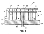
Figures 1 is a cross sectional view of one embodiment of the invention, represented aselectrostatic chuck 10.Electrostatic chuck 10 can be, for example, of Coulombic type or of Johnson-Rahbek type, with the latter being preferred.Electrostatic chuck 10 includeschuck body 12 and, withinchuck body 12,electrode 14. -
Electrode 14 can be a foil, a plate, a perforated foil or a perforated plate, a mesh, a screen printed layer or can have some other configuration that is suitable for incorporation into electrostatic chucks.Electrode 14 can be used as a chucking electrode, a plasma generating electrode or both. If the electrode operates as a chucking electrode only, a preferred thickness of the electrode is in a range of between about 10µm (micrometers or microns) and about 50µm Generally, a plasma generating electrode is thick enough to withstand the radio frequency (RF) applied to it. The preferred thickness of a plasma generating electrode ranges from about 50µm to about 1 mm (millimeters). A suitable of a mesh electrode has a wire diameter of about 125 µm and a mesh spacing of 19.6 wires per cm (50 wires per inch). In one embodiment,electrode 14 is a flat film electrode such as described inU.S. Provisional Patent Application 60/169,859 -
Electrode 14 is fabricated from a suitable metal or from a combination of metals or alloy. In a preferred embodiment,electrode 14 includes molybdenum (Mo), tungsten (W) or combinations of molybdenum and tungsten. Optionally, a Mo, W or Mo-W electrode includes additional metals, such as nickel and cobalt or other components such as sintering activators. Other suitable metals for fabricating ofelectrode 14 include, but are not limited to, tantalum, platinum, hafnium, rhodium, vanadium and alloys thereof. In one embodiment, the electrode material is graphite. - Chuck
body 12 includesdielectric layer 16, atupper side 18 ofelectrode 14, andsubstrate 20, atlower side 22 ofelectrode 14. In one embodiment of the invention,electrode 14 is completely and integrally embedded withinchuck body 12. In another embodiment,electrode 14 is sandwiched betweendielectric layer 16 andsubstrate 20. A joint or seam (not shown) bindsdielectric layer 16 tosubstrate 20. A joint or seam that does not allow ambient atmosphere to interact withelectrode 14 is preferred. In one embodiment of the invention, the joint or seam is formed by employing a suitable brazing material. In another embodiment, the brazing material employed to form the join or seam also functions aselectrode 14. Alternatively, there is no joint or seam betweendielectric layer 16 andsubstrate 20. - In one embodiment, the thickness of
dielectric layer 16, ranges from about 10 µm to about 5mm. In another embodiment, the dielectric resistivity ofdielectric layer 16 is greater than 1013 ohm•cm, at the operating temperature of the chuck, which is particularly suitable in the case of a Coulombic-type chuck. In yet another embodiment, the dielectric resistivity ofdielectric layer 16 ranges from about 108 to about 1013 ohm•cm, at the operating temperature of the chuck, which is particularly suitable for a Johnson-Rahbek-type electrostatic chuck. - Materials which can be employed to fabricate
chuck body 12,dielectric layer 16 and/orsubstrate 20 include but are not limited to aluminum oxide (Al2O3), aluminum oxide-titanium oxide (Al2O3-TiO2), aluminum nitride (AlN), silicon nitride (Si3N4), silicon carbide (SiC), boron nitride (BN), yttrium oxide or yttria (Y2O3), yttrium aluminate (for example, Y3Al5O12, YAlO3, Al2Y4O9) and any combination thereof. AlN is preferred. In one embodiment of the invention, chuckbody 12 has an uniform chemical composition. Alternatively, chuckbody 12 can be constructed from different materials; for example, the chemical composition ofsubstrate 20 can differ from that ofdielectric layer 16. - Chuck
body 12,dielectric layer 16 and/orsubstrate 20 also can include additional components, for example, sintering aids, bonding agents and other materials, known in the art. Examples of additional components include but are not limited to yttrium oxide (Y2O3), calcium salts and oxides, for instance, calcium fluoride or CaF2, calcium chloride or CaCl2, calcium oxide or CaO, calcium carbonate or CaCO3, calcium nitrate or Ca(NO3)2, chromium oxide (Cr2O3), silica (SiO2), boron nitride (BN) and any combination(s) thereof, as well as secondary phases, formed by reaction(s) between the ceramic material and the additional component(s), such as, for example, compounds including yttrium aluminum and oxygen, for example, Y3Al5O12, YAlO3, Al2Y4O9 or combinations thereof. Compounds which include yttrium aluminum and oxygen are also referred to herein as yttrium aluminates. In one embodiment anAlN chuck body 12,dielectric layer 16 and/orsubstrate 20 can also include Al2O3, an oxynitride of aluminum, (for example AlON), Y2O3, CaF2 CaCl2, CaO, CaCO3, Ca(NO3)2, Cr2O3, SiO2, BN, Y3Al5O12, YAlO3, Al2Y4O9 or combinations thereof. - Optionally,
electrostatic chuck 10 can further include a heating element (not shown). One suitable arrangement of an electrostatic chuck which includes an embedded heating element is described inU.S. Patent Application 09/457,968 -
Electrostatic chuck 10 has backsurface 24 and chuckingsurface 26. Optionally, chuckingsurface 26 includesprotrusions 28 andchannels 30. A surface pattern such as one including, for example, protruding dimples or ridges significantly reduces contact area between work-piece 32 and chuckingsurface 26, and allows heat transfer fluid to circulate beneath work-piece 32. Optionally, chuckingsurface 26 can be coated, for example, for enhanced erosion and/or corrosion resistance. Coatings which can be applied onto chuckingsurface 26 include but are not limited to pyrolytic BN, yttria, an yttrium aluminate, aluminum trfluoride (AlF3), diamond and diamond-like coatings, such as, for example, coatings applied by chemical vapor deposition (CVD) methods. Thin coatings are preferred, such as, for example, coatings ranging from about 1 micrometer (µm) to about 100 µm in thickness. - During operation, power is supplied to
electrode 14 throughelectrical connector 34.Electrical connector 34 is attached toelectrode 14 through means known in the art. For exampleelectrical connector 34 can be brazed toelectrode 14. In one embodiment of the invention, a contact plug (not shown) is co-sintered to the electrode and joined toelectrical connector 34. Contacts and/or electrical connectors that have good electrical conductivity, low RF impedence and are easily joined toelectrode 14 are preferred. In one embodiment of the invention,electrical connector 34 includes, atelectrode 14, an electrical contact such as described inU.S. Patent Application 09/457,968 -
Electrostatic chuck 10 also includes one or more lift pin holes 36 which accommodate lift pins typically employed to raise or lower work-piece 32 from chuckingsurface 26. Generally, lift pin holes 36 extend fromback surface 24, throughsubstrate 20,electrode 14,dielectric layer 16, to chuckingsurface 26.Electrode 14 has apertures which align with lift pin holes 36 but, preferably, are larger in diameter, thereby preventing the lift pins from contactingelectrode 14. The number of lift pin holes 36 generally depends on the chuck design and its application. -
Electrostatic chuck 10 includes at least oneconduit 38 which provides fluid communication betweenback surface 24 and chuckingsurface 26. Generallyconduit 38 extends fromback surface 24, throughsubstrate 20,electrode 14,dielectric layer 16, to chuckingsurface 26. To accommodateconduit 38electrode 14 has apertures which align withconduit 38 and, preferably, are larger in diameter, thereby preventing heat transfer gas flowing throughconduit 38 from contactingelectrode 14. The cross section ofconduit 38 can have, for example, a circular, elliptical, ring-like shape or any other suitable shape. - Either or both the shape or dimensions of the cross section of
conduit 38 can be essentially constant throughout the thickness ofelectrostatic chuck 10. Alternatively, either or both the shape or dimensions ofconduit 38 can vary betweenback surface 24 and chuckingsurface 26. -
Conduit 38 includes porous zone orregion 40 which is integrated withinchuck body 12.Porous region 40 can include a ceramic material such as, for example, AlN, Si3N4, Al2O3, Al2O3-TiO2, SiC. Optionally,porous region 40 can further include one or more components such as, for example, additives, sintering aids or bonding agents. Examples of additional components include but are not limited to yttrium oxide (Y2O3), calcium salts and oxides, for instance, calcium fluoride or CaF2, calcium chloride or CaCl2, calcium oxide or CaO, calcium carbonate or CaCO3, calcium nitrate or Ca(NO3)2, chromium oxide (Cr2O3), silica (SiO2), boron nitride (BN) and any combination(s) thereof.Porous region 40 also can include reaction products, also referred to herein as secondary phases, formed by reaction(s) between the ceramic material and the additional component(s). In a preferred embodiment,porous region 40 includes AlN and an yttrium aluminate, such as, for example, Y3Al5O12, YAlO3, Al2Y4O9 or combinations thereof.Porous region 40 can also include Al2O3 or an oxynitride of aluminum, for example AlON. In another embodiment,porous region 40 includes AlN and Y2O3, CaF2, CaCl2, CaO, CaCO3, Ca(NO3)2, Cr2O3, SiO2, BN or a combination(s) thereof.Porous region 40 can be fabricated from the same material employed to fabricatedielectric layer 16 or chuckbody 12. - Generally
porous region 40 has a porosity sufficient to allow a required gas flow to the chucking surface. Pores small enough to restrict plasma penetration intoconduit 38 are preferred. Also preferred are pores which do not form a direct line of sight between the backside (side resting on electrostatic chuck 10) ofworkpiece 32,electrode 14 andcathode pedestal 42, which supportselectrostatic chuck 10. - The porosity and average pore size employed can vary depending on the chuck design and/or application of a particular chuck. In one embodiment, the porosity of
porous region 40 is in a range of between about 10% and about 60% and preferably in a range of between about 30% and about 50%. In another embodiment, average pore size ranges from about 5 µm to about 500 µm, with preferred pores having an average size between from about 20 µm to about 100 µm. -
Porous region 40 is integrated or integrally bonded to chuckbody 12. As used herein, the terms "integrated" or "integrally bonded" mean thatporous region 40 is part ofchuck body 12. For example, the interface betweenporous region 40 and chuckbody 12 does not present cracks, seams, joints or other defects. In a preferred embodiment,porous region 40 is diffusion-bonded to surroundingchuck body 12. In another preferred embodimentporous region 40 is chemically bonded to surroundingchuck body 12.Porous region 40 can also be sintered into surroundingchuck body 12. - In a preferred embodiment of the invention, a plurality of
conduits 38, which includeporous region 40, are employed. The number, dimensions and arrangement ofporous regions 40 can depend, for example, upon the design and/or application of a particular chuck.Porous regions 40 can but need not have the same porosity. In one embodiment of the invention, most or all ofchuck body 12 is porous. Alternatively, most or all ofdielectric layer 16 is porous. - In one embodiment, all
porous regions 40 have the same shape. In another embodiment allporous regions 40 have the same dimensions. In still another embodimentelectrostatic chuck 10 includes porous regions having different shapes. Some suitable cross sectional shapes ofporous region 40 are shown inFigure 3 . - In a preferred embodiment,
porous region 40 is a porous plug, such as, for example, a cylindrical porous plug. The number, dimensions and arrangement of the porous plugs can depend, for example, upon the design and/or application of a particular chuck. In one embodiment, the diameter of the porous plug ranges from about 0.5 millimeter (mm) to about 20 mm. In another preferred embodiment,electrostatic chuck 10 has between about 1 and about 100 porous plugs, and preferably between about 20 and about 50 porous plugs. - In another preferred embodiment,
electrostatic chuck 10 includesporous regions 40 which are concentric rings. In a further embodiment, the surface area at the chucking surface of one ring is greater than the surface area of another ring. In yet another embodiment, the porosity of the ring having the greater surface area is less than that of the ring which has the smaller surface area. - Preferably,
porous region 40 prevents the formation of a direct line of sight from workpiece 32 (in particular from the side ofworkpiece 32 which rests on electrostatic chuck 10) toelectrode 14 and tocathode pedestal 42. In one embodiment of the invention,porous region 40, integrally bonded to chuckbody 12, extends fromback surface 24 to chuckingsurface 26, as shown inFigure 1 . Alternatively,porous region 40, also integrally bonded to chuckbody 12, only partially extends throughconduit 38. -
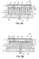
Figures 3A is a cross sectional view of one embodiment of the invention, - represented aselectrostatic chuck 44.Electrostatic chuck 44 includesconduit 38 to provide fluid communication betweenback surface 24, and chuckingsurface 26.Conduit 38 includesporous region 40, at backsurface 24.Porous region 40 is in the shape of a porous plug and is integrally bonded tosubstrate 20.Porous region 40 partially extends fromback surface 24 throughconduit 38, towards, but not all the way to, chuckingsurface 26.Conduit 38 also includesopening 46, which does not include porous material and which extends fromporous zone 40 to chuckingsurface 26. Porosity and other pore-related properties, the numbers and volume ofporous regions 40, the diameter and number ofopenings 46 are factors which can vary from one chuck design to another, depending on the application and the desired volume flow of heat transfer fluid. -
Figures 3B is a cross sectional view of an example, represented aselectrostatic chuck 48.Electrostatic chuck 48 includesporous region 40 at backsurface 24.Porous region 40 is integrally bonded tosubstrate 20. It partially extends fromback surface 24, some distance towards, but not all the way to, chuckingsurface 26. The cross section ofporous region 40 can be, for example, elliptical, a ring or another suitable shape, such as a shape illustrated inFigure 2 . Alternatively, most or the entire volume at backsurface 24, extending fromback surface 24 towards, but not all the way to, chuckingsurface 26, can be porous.Electrostatic chuck 48 also includesopenings 46, which do not include porous material and extend fromporous region 40 to chuckingsurface 26. As discussed above, porosity and other pore-related properties, numbers and volume ofporous regions 40, the diameter and number ofopenings 46 are factors which can vary from one chuck design to another, depending on the application and the desired volume flow of heat transfer fluid. - In yet other embodiments, (not shown), the porous region is at the chucking surface and is integrally bonded to the dielectric layer of the chuck body. The porous region extends from the chucking surface through the chuck body towards, but not all the way to, the back surface. For example, the porous region extends from the chucking surface through the electrode. One or more openings for directing heat transfer fluid extend from the porous region to the back surface.
- Porous regions which partially extend through the conduit between the back surface and the chucking surface and are integrally bonded to the chuck body can be placed in other zones within the conduit, for example, away from both the back surface and the chucking surface. Electrostatic chucks which combine porous regions which extend from back surface to the chucking surface and porous regions which only partially extend through the conduit also can be fabricated.
- During the operation of
electrostatic chuck 10 shown inFigure 1 , a heat transfer fluid is directed, from backsurface 24, throughporous region 40 to chuckingsurface 26. Similarly, in the case ofelectrostatic chucks Figures 3A and 3B , a heat transfer fluid is directed fromback surface 24, through porous region(s) 40,openings 46 to chuckingsurface 26. - The heat transfer fluid exits at chucking
surface 26 and, optionally, circulates thoughchannels 22, thereby modifying the temperature of work-piece 32. Heat transfer fluid can be supplied from a source, not shown in the figures and directed toporous region 40, for example, through an opening incathode pedestal 42. Heat transfer fluid can be supplied toporous region 40 via tubings, pipings, regulators, fittings, valves, plenum reservoir(s), any combinations thereof, or other suitable means known in the art. - Examples of heat transfer fluids include, but are not limited to, helium, argon, or other inert gases, as well as gases which are inert in the particular operation, environment and conditions in which electrostatic chuck is employed, and mixtures thereof. The heat transfer fluid can be at a temperature suitable in effecting the desired modification of the work-piece temperature. Heat transfer fluid within a desired temperature range can be supplied to chuck 10 as known in the art, for example by heating of cooling the heat transfer fluid in a heat exchanger, or by using cryogenic fluids. The pressure of heat transfer fluid supplied to
conduit 38 can be controlled as known in the art. Preferably, the heat transfer fluid is supplied at a pressure such that the flow of heat transfer fluid exiting at chuckingsurface 26 does not interfere with the electrostatic forces exerted upon work-piece 32 and the operation of the electrostatic chuck. - As discussed above, design parameters such as, for example, the porosity, pore size and volume of the porous regions can be chosen to obtain a desired volume flow. A desired gas conductance is dependent on the size of pores and the amount of porosity in
porous region 40. Gas conductance is the volume of gas allowed to flow through at a given pressure. The porosity of a large porous region can be adjusted, for example, to yield an equivalent gas conductance of a small porous plug. - The invention also is related to methods of producing an electrostatic chuck.
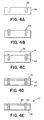
- Stages of one embodiment of a method of the invention are shown in
Figures 4A through 4E . As shown inFigure 4A ,first portion 50 of a green chuck body includesrecess 52. As used herein, "green" refers to the pre-densified state of a ceramic precursor. The green chuck body can be a compacted (for example cold-pressed), non-densified body of a precursor, such as, for example a powder or slurry, which upon densification will form a ceramic body. In a preferred embodiment,first portion 50 is formed by compacting AlN powder. Other suitable materials which can be employed include, but are not limited to, AlN, Si3N4, Al2O3, Al2O3-TiO2 or SiC, BN, Y2O3, yttrium aluminates or any combination thereof. -
Plug 54 is positioned intorecess 52, as shown inFigure 4B .Plug 54 can have any suitable shape, as discussed above. More than oneplug 54 can be incorporated in the green body. Optionally, plug 54 can be surrounded by a dense sleeve, which is co-sintered aroundplug 54. -
Plug 54 is in a green form which can be compacted intorecess 52. For instance, plug 54, in its green form can be a powder compacted intorecess 52 or can be a cold pressed green pellet molded to fit intorecess 52. Withplug 54 being its green form, allowance is made for its shrinkage during densification along with shrinkage of firstgreen portion 50, as is known in the art.Plug 54 becomes porous upon densification or as a result of another processing step (for example during heat treatment or soaking) or by treatment with an agent as further described below. - Suitable materials which can be employed to form the green form of
plug 54 include, but are not limited to, AlN, Si3N4, Al2O3, Al2O3-TiO2, SiC. AlN, BN, Y2O3, yttrium aluminates or any combination thereof is preferred. The same material can be employed to form both the green body and the green form ofplug 54. - In one embodiment, plug 54, in its green form, includes removable particles. Removable particles can be in the form of powders, beads, granules, spheres, chopped fibers, filaments or can have other suitable shapes. Particles having an uniform size, as known in the art, also can be employed. The amount, shape and particle sizes employed can be selected to result, upon the removal of the particles, in a porous region having a desired porosity and a desired pore size range as discussed above.
- Removable particles can include compounds which decompose or burn off at the temperatures employed in the manufacture of electrostatic chucks. For example, removable particles can include organic compounds, polymers, metal complexes, organometallic compounds and other fugitive materials which decompose or burn off, for example during heat treating, soaking, sintering or hot pressing. Clean burning fugitive compounds, which do not cause undesirable emissions are preferred. Particularly preferred are polymers of acrylic or methacrylic acid, for example polymethylmethacrylate (PMMA). Polystyrene, polyethylene, acrylic resins, cellulose acetate, cured epoxy resins, polyimide resins are examples of other materials which can be included in the green body. Copolymers, ter-polymers as well as cross-linked modifications thereof also can be employed.
- In another embodiment, removable particles are removed by treatment with a chemical agent. For instance, the green form of
plug 54 can include metal particles which can be removed, preferably after densification of the green body, by etching with a suitable chemical agent, for example, a mixture of HF and HNO3. Preferably, a continuous phase of a metal such as, for example, molybdenum (Mo), tungsten (W), rhodium (Rh), vanadium (V), niobium (Nb), hafnium (Hf) and other refractory metals or alloys thereof is employed. - The green form of
plug 54 also can include one or more additional components. In a preferred embodiment, the green form ofplug 54 includes one or more components that serve as a bonding agent and/or as a sintering aid. Nonlimiting examples of additional components which can be included in the green are: Y2O3, CaF2, CaCl2, CaO, CaCO3, Ca(NO3)2, Cr2O3, SiO2, BN, combinations thereof as well as other commonly used sintering aids. In another preferred embodiment, the additional component(s) form a liquid phase during sintering. Alternatively, the green form ofplug 54 does not include a sintering and/or bonding agents. - The green form of
plug 54 also can be formed from a coarse powder which, upon densification, results in a porous region such as described above. - In one embodiment of the invention, a sintering inhibitor such as magnesium oxide (MgO), silica (SiO2), silicates, such as, for example, aluminum silicate or magnesium silicate, carbon (in excess of the carbon amount required to reduce oxygen) or another suitable sintering inhibitor can be added to a desired region in the green body. The sintering inhibitor prevents complete densification in that region and upon densification conditions, the incompletely densified region is porous.
- As shown in
Figure 4C ,electrode 14 is positioned onto firstgreen portion 50 of the green chuck body.Electrode 14 can be, for example, a mesh electrode, in which case mesh openings can be arranged concentrically aroundplug 54. Alternatively,electrode 14 can be a screen printed layer, a foil or plate provided with apertures which align concentrically but are larger in diameter thanplug 54, thereby preventing the electrode material from contactingplug 54. If a dense sleeve, co-sintered aroundplug 54, is employed, hole perforation intoelectrode 14 is simplified since the dense sleeve serves as a barrier betweenplug 54 andelectrode 14. -
Second portion 56 of a green chuck body is overlaid ontoelectrode 14.Second portion 56 includes a dielectric material. Ceramic precursors and additional components which are suitable in formingfirst portion 50 also can be employed in formingsecond portion 56. In a preferred embodiment, bothfirst portion 50 andsecond portion 56 have the same composition. - The resulting assembly is densified, for example, by sintering to obtain a dense structure having porous region 40 (in this case a porous plug), which is integrally bonded to chuck
body 12 as shown inFigure 4D . Sintering can be in the absence of pressure (pressure less sintering) or by hot pressing. The sintering temperature can depend on the particular materials employed in the fabrication of the electrostatic chuck. In the case of an AlN compacted powder, the sintering temperature ranges from about 1500°C to about 2000°C. If sintering is conducted under pressure, the pressure can range from about 10 MPa (mega Pascal) to about 40 MPa. In one embodiment of the invention, a dense sleeve co-sintered to the plug is employed, as described above, thereby preventing a possible collapse of the plug during hot pressing. - Sintering can be under an inert atmosphere, as described in
U.S. Patent Application No. 09/458,278 - The ends of
porous region 40 are exposed atback surface 24 and at chuckingsurface 26, for example by machining, thereby formingelectrostatic chuck 10, shown inFigure 4E . - A method for obtaining an electrostatic chuck having a partially extended porous region or plug, for example at back
surface 26, includes the steps shown inFigures 4A and 4B , as described above.First portion 50 of a green chuck body, includingplug 54 are then densified, for example, by a method described above, after which they are overlayed byelectrode 14 andsecond portion 56. The resulting assembly is exposed to conditions such, for example, as hot pressing or pressureless sintering, which result in densification ofsecond portion 56. An opening extending from chuckingsurface 26 toporous region 40 is formed, for example by machining. Alternatively, a pin inserted into the green form ofsecond portion 56, prior to its densification, can be removed, leaving behind the desired opening. The end ofporous plug 40 is exposed atback surface 24 as described above. - Another method of producing an electrostatic chuck includes integrating a porous plug into a dense chuck body. The chuck body and the porous plug can be fabricated separately, for example, from materials and by methods described above. In one embodiment of the invention, the porous plug itself is fabricated by densifying a green form of a plug which includes fugitive materials. The plug can include or can be coated with a bonding agent, such as the bonding agents described above. In the case of an AlN chuck bodies and AlN porous plug, Y2O3, Y3Al5O12, YAlO3, Al2Y4O9 and combinations thereof are preferred. Al2O3 or oxynitrides of Al also can be employed as bonding agents. Bonding agents amounts, with respect to the porous region, generally range from about 0.5 weight % to about 10 weight %. If a high purity electrostatic chuck is desired, minimum amounts of bonding agents necessary to effect bonding of the plug to the chuck body are preferred.
- Integration of the porous plug into the surrounding chuck body can be accomplished by heating to a temperature sufficient to effect diffusion bonding between the porous plug and the chuck body. Alternatively, the temperature can be high enough to soften or to liquify the bonding agent thereby joining the porous plug to the chuck body.
- 80 g of spray dried AlN powder containing 3 wt% of Y2O3 as a sintering aid was dry blended with 20 g of polymethylmethacrylate (PMMA), i.e., 20 wt% of PMMA. The PMMA was in the form of spherical beads approximately 50 µm in diameter. The mixture was then cold pressed at 210 MPa to form several "green" cylindrical plugs approximately 12.5 mm (0.5 in) in diameter and 22 mm (0.86 in) long. A second batch of "green" porous plug precursors was fabricated in identical fashion except that the weight fraction of the 50 µm PMMA was 30%. A third batch of "green" porous plug precursors was fabricated in identical fashion except that the size of the PMMA beads was approximately 100 µm (-120/+170 mesh) and the weight fraction of PMMA used was 30%. In order to remove the binders from the green body, each batch of green plug precursors was placed in an oven and heated in air to 600°C at a heating rate of 0.4°C/min, held for one hour at 600°C and cooled back to room temperature. These plugs were then sintered at 1850°C for one hour in nitrogen to obtain sintered porous plugs.
- One porous plug from each batch was characterized by mercury porosimetry and the results are shown in Table 1.
Table 1 Fugitive Added: PMMA Porous Plug Attributes Example Weight Fraction,% Size, µm Bulk Density, g/cm3 Porosity, % 1 20 50 2.31 27.3 2 30 50 1.94 40.8 3 30 100 1.94 42.1 - As can be seen from Table 1, porous plugs based on A1N with porosities of 27 to 42% were obtained.
- Three equally sized holes, spaced 120° apart, were machined into a 75 mm diameter body of hot-pressed, high purity A1N. Three A1N porous plugs from Example 3 were machined such that their outer diameter matched the diameter of the holes in the AlN body. One porous plug was then inserted into each hole in the A1N body. The assembly was heated in a furnace to 1850°C, soaked at 1850°C for an hour, and subsequently cooled to room temperature. Upon inspection, it was discovered that all three porous plugs had fused to the A1N body. Air was passed through the porous plugs to verify that the plugs had adequate conductance.
- The same experiment was repeated with another identical assembly of porous plugs in an A1N body with the dual purpose of joining the plugs to the A1N body as well as adjusting the resistivity of the A1N body. The assembly was heat treated at 1750°C for 4 hours in argon and then cooled to room temperature. Once again, the porous plugs had bonded to the main A1N body and had adequate (gas) conductance. In addition, the resistivity of the A1N body was 5x10¹⁰ ohm•cm (measured at room temperature and an electric field of 500 V/mm).
- While this invention has been particularly shown and described with references to preferred embodiments thereof, it will be understood by those skilled in the art that various changes in form and details may be made therein without departing from the scope of the invention encompassed by the appended claims.
Claims (31)
- An electrostatic chuck, comprising:a) a chuck body (12) having a back surface (24) and a chucking surface (26);b) an electrode (14) within said chuck body (12); andc) a plurality of conduits (38) extending between the back surface (24) and the chucking surface (26) to provide fluid communication therebetween, each conduit (38) containing therein a porous region (40) that is an integral part of said chuck body (12).
- The electrostatic chuck of Claim 1, wherein the chuck body (12) is a ceramic chuck body.
- The electrostatic chuck of Claim 2, wherein the porous regions (40) extend from the back surface (24) to the chucking surface (26) of the electrostatic chuck.
- The electrostatic chuck of Claim 2, wherein the porous regions (40) partially extend through respective conduits (38).
- The electrostatic chuck of Claim 3, wherein the porous regions (40) are at the back surface (24).
- The electrostatic chuck of Claim 3, wherein the porous regions (40) are at the chucking surface (26).
- The electrostatic chuck of Claim 2, wherein the chemical composition of the chuck body (12) and of the porous regions (40) are essentially the same.
- The electrostatic chuck of Claim 7, wherein the porous regions (40) include a bonding component.
- The electrostatic chuck of Claim 8, wherein the bonding component includes an yttrium aluminate or yttria.
- The electrostatic chuck of Claim 9, wherein the yttrium aluminate includes at least one member selected from the group consisting of Y3Al5O12, YAlO3 and Al2Y4O9.
- The electrostatic chuck of Claim 8, wherein the ceramic chuck body (12) includes a bonding component.
- The electrostatic chuck of Claim 1, wherein the electrode (14) includes an upper side (18) and a lower side (22), and wherein the chuck body (12) includes:a) a first dielectric layer (16) between said upper side (18) and the chucking surface (26); andb) a substrate (20) between said lower side (22) and the back surface (24), the porous regions (40) being an integral part of either or both said first dielectric layer (16) or said substrate (20).
- The electrostatic chuck of Claim 12, wherein the first dielectric layer (16) is in a range of between about 10µm and about 5mm.
- The electrostatic chuck of Claim 1, wherein the ceramic chuck body (12) and the porous regions (40) include at least one member selected from the group consisting of aluminum nitride, Al2O3, Al2O3-TiO2, Si3N4, SiC, BN, Y2O3 and an yttrium aluminate.
- The electrostatic chuck of Claim 1, wherein the porous regions (40) have a porosity in a range of between about 10% and about 60%.
- The electrostatic chuck of Claim 1, wherein the porous regions (40) have a cylindrical shape.
- The electrostatic chuck of Claim 1, wherein the porous regions (40) include at least one ring.
- The electrostatic chuck of Claim 1, wherein the porous regions (40) include concentric rings.
- The electrostatic chuck of Claim 18, wherein the concentric rings include a first ring and a second ring, wherein the surface area of the first ring at the chucking surface (26) is greater than that of the second ring, and wherein the porosity of the first ring is less than that of the second ring.
- The electrostatic chuck of Claim 1, further including lift pin holes (36).
- A method of producing an electrostatic chuck, comprising the steps of:a) forming in a green body of an electrostatic chuck body a plurality of green regions (54) that, following densification of the green body, will be porous; andb) densifying the green body, thereby forming the ceramic electrostatic chuck body (12), said ceramic electrostatic chuck body (12) including a plurality of conduits (38) extending between the back surface (24) and the chucking surface (26), each conduit (38) including a porous region (40) which corresponds to a former green region (54).
- The method of Claim 21, wherein the green regions (54) include a sintering aid.
- The method of Claim 22, wherein the green regions (54) include at least one sintering aid selected from the group consisting of Y2O3, a calcium halide, a calcium oxide, a calcium nitrate, Cr2O3, SiO2 and BN.
- The method of Claim 23, wherein the green regions (54) include Y2O3.
- The method of Claim 21, wherein the green regions (54) include a polymer component that, during densification of the green body, will decompose, thereby leaving pores and forming the porous regions of the electrostatic chuck body.
- The method of Claim 25, wherein the green regions (54) include at least one polymer selected from the group consisting of polymethylmethacrylate, polystyrene, polyethylene, acrylic resin, vinyl resin, cellulose acetate, cured epoxy resin, polyimide resin, co-polymer, ter-polymer and cross-linked modifications thereof.
- The method of Claim 21, wherein the green regions (54) include at least one member from the group consisting of Al2O3, Al2O3-TiO2, Si3N4, SiC, BN, Y2O3 and an yttrium aluminate.
- The method of Claim 21, wherein the green regions (54) include at least one pre-densified portion.
- The method of Claim 21, wherein the green body is densified by pressureless sintering.
- The method of Claim 21, wherein the green body is densified by hot pressing.
- A method of modifying a wafer's process temperature, comprising the steps of:a) supporting the wafer on a chucking surface (26) of the electrostatic chuck according to any of the claims 1 to 20 andb) directing a heat transfer fluid through the plurality of conduits (38) to the chucking surface (26), thereby modifying the wafer's process temperature.
Applications Claiming Priority (3)
| Application Number | Priority Date | Filing Date | Title |
|---|---|---|---|
| US09/655,324 US6606234B1 (en) | 2000-09-05 | 2000-09-05 | Electrostatic chuck and method for forming an electrostatic chuck having porous regions for fluid flow |
| US655324 | 2000-09-05 | ||
| PCT/US2001/024135 WO2002021590A2 (en) | 2000-09-05 | 2001-08-01 | Electrostatic chuck with porous regions |
Publications (2)
| Publication Number | Publication Date |
|---|---|
| EP1316110A2 EP1316110A2 (en) | 2003-06-04 |
| EP1316110B1 true EP1316110B1 (en) | 2008-12-10 |
Family
ID=24628428
Family Applications (1)
| Application Number | Title | Priority Date | Filing Date |
|---|---|---|---|
| EP01955029A Expired - Lifetime EP1316110B1 (en) | 2000-09-05 | 2001-08-01 | Electrostatic chuck with porous regions |
Country Status (9)
| Country | Link |
|---|---|
| US (1) | US6606234B1 (en) |
| EP (1) | EP1316110B1 (en) |
| JP (1) | JP4959905B2 (en) |
| KR (1) | KR100557695B1 (en) |
| AT (1) | ATE417358T1 (en) |
| AU (1) | AU2001277237A1 (en) |
| DE (1) | DE60136940D1 (en) |
| TW (1) | TW526521B (en) |
| WO (1) | WO2002021590A2 (en) |
Cited By (2)
| Publication number | Priority date | Publication date | Assignee | Title |
|---|---|---|---|---|
| US20200273736A1 (en) * | 2017-09-29 | 2020-08-27 | Sumitomo Osaka Cement Co., Ltd. | Electrostatic chuck device |
| WO2023150006A1 (en) * | 2022-02-03 | 2023-08-10 | Applied Materials, Inc. | Electrostatic chuck with porous plug |
Families Citing this family (55)
| Publication number | Priority date | Publication date | Assignee | Title |
|---|---|---|---|---|
| AU2002231654A1 (en) * | 2000-12-07 | 2002-06-18 | Byk Gulden Lomberg Chemische Fabrik G.M.B.H. | Pharmaceutical paste comprising an acid-labile active ingredient |
| TWI234417B (en) * | 2001-07-10 | 2005-06-11 | Tokyo Electron Ltd | Plasma procesor and plasma processing method |
| US6490145B1 (en) * | 2001-07-18 | 2002-12-03 | Applied Materials, Inc. | Substrate support pedestal |
| TW561515B (en) * | 2001-11-30 | 2003-11-11 | Tokyo Electron Ltd | Processing device, and gas discharge suppressing member |
| US20030219986A1 (en) * | 2002-05-22 | 2003-11-27 | Applied Materials, Inc. | Substrate carrier for processing substrates |
| KR100457833B1 (en) * | 2002-05-24 | 2004-11-18 | 주성엔지니어링(주) | Plasma Etching Apparatus |
| JP4095842B2 (en) * | 2002-06-26 | 2008-06-04 | 日本特殊陶業株式会社 | Electrostatic chuck |
| JP2004306191A (en) * | 2003-04-07 | 2004-11-04 | Seiko Epson Corp | Table device, film deposition device, optical element, semiconductor device and electronic equipment |
| DE102004060625A1 (en) * | 2004-12-16 | 2006-06-29 | Siltronic Ag | Coated semiconductor wafer and method and apparatus for producing the semiconductor wafer |
| US7235139B2 (en) * | 2003-10-28 | 2007-06-26 | Veeco Instruments Inc. | Wafer carrier for growing GaN wafers |
| US7245357B2 (en) * | 2003-12-15 | 2007-07-17 | Asml Netherlands B.V. | Lithographic apparatus and device manufacturing method |
| US7220497B2 (en) * | 2003-12-18 | 2007-05-22 | Lam Research Corporation | Yttria-coated ceramic components of semiconductor material processing apparatuses and methods of manufacturing the components |
| US20060023395A1 (en) * | 2004-07-30 | 2006-02-02 | Taiwan Semiconductor Manufacturing Co., Ltd. | Systems and methods for temperature control of semiconductor wafers |
| US7544251B2 (en) * | 2004-10-07 | 2009-06-09 | Applied Materials, Inc. | Method and apparatus for controlling temperature of a substrate |
| JP4350695B2 (en) * | 2004-12-01 | 2009-10-21 | 株式会社フューチャービジョン | Processing equipment |
| US7731798B2 (en) * | 2004-12-01 | 2010-06-08 | Ultratech, Inc. | Heated chuck for laser thermal processing |
| WO2006088448A1 (en) * | 2005-02-16 | 2006-08-24 | Veeco Instruments Inc. | Wafer carrier for growing gan wafers |
| WO2007081032A1 (en) * | 2006-01-11 | 2007-07-19 | Ngk Insulators, Ltd. | Electrode device for plasma discharge |
| US20080009417A1 (en) * | 2006-07-05 | 2008-01-10 | General Electric Company | Coating composition, article, and associated method |
| US7983017B2 (en) * | 2006-12-26 | 2011-07-19 | Saint-Gobain Ceramics & Plastics, Inc. | Electrostatic chuck and method of forming |
| US9202736B2 (en) * | 2007-07-31 | 2015-12-01 | Applied Materials, Inc. | Method for refurbishing an electrostatic chuck with reduced plasma penetration and arcing |
| US8108981B2 (en) * | 2007-07-31 | 2012-02-07 | Applied Materials, Inc. | Method of making an electrostatic chuck with reduced plasma penetration and arcing |
| US7848076B2 (en) * | 2007-07-31 | 2010-12-07 | Applied Materials, Inc. | Method and apparatus for providing an electrostatic chuck with reduced plasma penetration and arcing |
| JP2008172255A (en) * | 2008-01-25 | 2008-07-24 | Ngk Spark Plug Co Ltd | Electrostatic chuck |
| US8681472B2 (en) * | 2008-06-20 | 2014-03-25 | Varian Semiconductor Equipment Associates, Inc. | Platen ground pin for connecting substrate to ground |
| US8218284B2 (en) * | 2008-07-24 | 2012-07-10 | Hermes-Microvision, Inc. | Apparatus for increasing electric conductivity to a semiconductor wafer substrate when exposure to electron beam |
| US8094428B2 (en) * | 2008-10-27 | 2012-01-10 | Hermes-Microvision, Inc. | Wafer grounding methodology |
| US20100107974A1 (en) * | 2008-11-06 | 2010-05-06 | Asm America, Inc. | Substrate holder with varying density |
| US9218997B2 (en) * | 2008-11-06 | 2015-12-22 | Applied Materials, Inc. | Electrostatic chuck having reduced arcing |
| US20100177454A1 (en) * | 2009-01-09 | 2010-07-15 | Component Re-Engineering Company, Inc. | Electrostatic chuck with dielectric inserts |
| US20110024049A1 (en) * | 2009-07-30 | 2011-02-03 | c/o Lam Research Corporation | Light-up prevention in electrostatic chucks |
| US8916793B2 (en) | 2010-06-08 | 2014-12-23 | Applied Materials, Inc. | Temperature control in plasma processing apparatus using pulsed heat transfer fluid flow |
| US9338871B2 (en) | 2010-01-29 | 2016-05-10 | Applied Materials, Inc. | Feedforward temperature control for plasma processing apparatus |
| US8880227B2 (en) | 2010-05-27 | 2014-11-04 | Applied Materials, Inc. | Component temperature control by coolant flow control and heater duty cycle control |
| US8608852B2 (en) * | 2010-06-11 | 2013-12-17 | Applied Materials, Inc. | Temperature controlled plasma processing chamber component with zone dependent thermal efficiencies |
| US9728429B2 (en) | 2010-07-27 | 2017-08-08 | Lam Research Corporation | Parasitic plasma prevention in plasma processing chambers |
| US8906164B2 (en) | 2010-08-05 | 2014-12-09 | Lam Research Corporation | Methods for stabilizing contact surfaces of electrostatic chucks |
| JP5458050B2 (en) * | 2011-03-30 | 2014-04-02 | 日本碍子株式会社 | Manufacturing method of electrostatic chuck |
| US10274270B2 (en) | 2011-10-27 | 2019-04-30 | Applied Materials, Inc. | Dual zone common catch heat exchanger/chiller |
| JP5956379B2 (en) * | 2012-04-27 | 2016-07-27 | 日本碍子株式会社 | Components for semiconductor manufacturing equipment |
| KR102032744B1 (en) | 2012-09-05 | 2019-11-11 | 삼성디스플레이 주식회사 | Sealant dispenser and a method of sealing a display panel using the same |
| CN104748574A (en) * | 2013-12-27 | 2015-07-01 | 北京思能达节能电气股份有限公司 | System and method for monitoring baking state of self-baking electrode |
| US9976211B2 (en) | 2014-04-25 | 2018-05-22 | Applied Materials, Inc. | Plasma erosion resistant thin film coating for high temperature application |
| JP6202111B2 (en) * | 2014-11-20 | 2017-09-27 | 住友大阪セメント株式会社 | Electrostatic chuck device |
| WO2016135565A1 (en) | 2015-02-23 | 2016-09-01 | M Cubed Technologies, Inc. | Film electrode for electrostatic chuck |
| JP6722518B2 (en) * | 2016-06-09 | 2020-07-15 | 新光電気工業株式会社 | Sintered body, method of manufacturing the same, and electrostatic chuck |
| JP6854600B2 (en) * | 2016-07-15 | 2021-04-07 | 東京エレクトロン株式会社 | Plasma etching method, plasma etching equipment, and substrate mount |
| US20180025931A1 (en) * | 2016-07-22 | 2018-01-25 | Applied Materials, Inc. | Processed wafer as top plate of a workpiece carrier in semiconductor and mechanical processing |
| US10975469B2 (en) * | 2017-03-17 | 2021-04-13 | Applied Materials, Inc. | Plasma resistant coating of porous body by atomic layer deposition |
| JP2019029384A (en) * | 2017-07-25 | 2019-02-21 | 新光電気工業株式会社 | Ceramic mixture, porous body and manufacturing method thereof, electrostatic chuck and manufacturing method thereof, and substrate fixing device |
| KR102039802B1 (en) * | 2017-12-19 | 2019-11-26 | 한국세라믹기술원 | Ceramic body for electrostatic chuck |
| US10411380B1 (en) | 2018-05-24 | 2019-09-10 | Microsoft Technology Licensing, Llc | Connectors with liquid metal and gas permeable plugs |
| US11456161B2 (en) * | 2018-06-04 | 2022-09-27 | Applied Materials, Inc. | Substrate support pedestal |
| CN111668148A (en) * | 2019-03-05 | 2020-09-15 | Toto株式会社 | Electrostatic chuck and processing apparatus |
| US20240112889A1 (en) * | 2022-09-30 | 2024-04-04 | Applied Materials, Inc. | Large diameter porous plug for argon delivery |
Family Cites Families (14)
| Publication number | Priority date | Publication date | Assignee | Title |
|---|---|---|---|---|
| JPS62155517A (en) * | 1985-12-27 | 1987-07-10 | Canon Inc | Apparatus and method for manufacturing semiconductor |
| US5542559A (en) | 1993-02-16 | 1996-08-06 | Tokyo Electron Kabushiki Kaisha | Plasma treatment apparatus |
| US5792562A (en) | 1995-01-12 | 1998-08-11 | Applied Materials, Inc. | Electrostatic chuck with polymeric impregnation and method of making |
| JPH0917770A (en) * | 1995-06-28 | 1997-01-17 | Sony Corp | Plasma treatment method and plasma apparatus used for it |
| JP3457477B2 (en) | 1995-09-06 | 2003-10-20 | 日本碍子株式会社 | Electrostatic chuck |
| US6399143B1 (en) | 1996-04-09 | 2002-06-04 | Delsys Pharmaceutical Corporation | Method for clamping and electrostatically coating a substrate |
| JPH09289201A (en) * | 1996-04-23 | 1997-11-04 | Tokyo Electron Ltd | Plasma treating apparatus |
| US6022807A (en) * | 1996-04-24 | 2000-02-08 | Micro Processing Technology, Inc. | Method for fabricating an integrated circuit |
| US5720818A (en) * | 1996-04-26 | 1998-02-24 | Applied Materials, Inc. | Conduits for flow of heat transfer fluid to the surface of an electrostatic chuck |
| US5835334A (en) | 1996-09-30 | 1998-11-10 | Lam Research | Variable high temperature chuck for high density plasma chemical vapor deposition |
| US6045753A (en) * | 1997-07-29 | 2000-04-04 | Sarnoff Corporation | Deposited reagents for chemical processes |
| US6004752A (en) * | 1997-07-29 | 1999-12-21 | Sarnoff Corporation | Solid support with attached molecules |
| JPH11260899A (en) * | 1998-03-10 | 1999-09-24 | Nippon Steel Corp | Electrostatic chuck |
| JP2001308075A (en) * | 2000-04-26 | 2001-11-02 | Toshiba Ceramics Co Ltd | Wafer support |
-
2000
- 2000-09-05 US US09/655,324 patent/US6606234B1/en not_active Expired - Lifetime
-
2001
- 2001-08-01 JP JP2002525911A patent/JP4959905B2/en not_active Expired - Lifetime
- 2001-08-01 EP EP01955029A patent/EP1316110B1/en not_active Expired - Lifetime
- 2001-08-01 WO PCT/US2001/024135 patent/WO2002021590A2/en active IP Right Grant
- 2001-08-01 AT AT01955029T patent/ATE417358T1/en not_active IP Right Cessation
- 2001-08-01 DE DE60136940T patent/DE60136940D1/en not_active Expired - Fee Related
- 2001-08-01 AU AU2001277237A patent/AU2001277237A1/en not_active Abandoned
- 2001-08-01 KR KR1020037003208A patent/KR100557695B1/en active IP Right Grant
- 2001-08-07 TW TW090119231A patent/TW526521B/en not_active IP Right Cessation
Cited By (4)
| Publication number | Priority date | Publication date | Assignee | Title |
|---|---|---|---|---|
| US20200273736A1 (en) * | 2017-09-29 | 2020-08-27 | Sumitomo Osaka Cement Co., Ltd. | Electrostatic chuck device |
| US11664261B2 (en) * | 2017-09-29 | 2023-05-30 | Sumitomo Osaka Cement Co., Ltd. | Electrostatic chuck device |
| WO2023150006A1 (en) * | 2022-02-03 | 2023-08-10 | Applied Materials, Inc. | Electrostatic chuck with porous plug |
| US11794296B2 (en) | 2022-02-03 | 2023-10-24 | Applied Materials, Inc. | Electrostatic chuck with porous plug |
Also Published As
| Publication number | Publication date |
|---|---|
| WO2002021590A3 (en) | 2002-08-01 |
| DE60136940D1 (en) | 2009-01-22 |
| KR100557695B1 (en) | 2006-03-07 |
| AU2001277237A1 (en) | 2002-03-22 |
| KR20030031177A (en) | 2003-04-18 |
| EP1316110A2 (en) | 2003-06-04 |
| JP4959905B2 (en) | 2012-06-27 |
| JP2004508728A (en) | 2004-03-18 |
| WO2002021590A2 (en) | 2002-03-14 |
| ATE417358T1 (en) | 2008-12-15 |
| TW526521B (en) | 2003-04-01 |
| US6606234B1 (en) | 2003-08-12 |
Similar Documents
| Publication | Publication Date | Title |
|---|---|---|
| EP1316110B1 (en) | Electrostatic chuck with porous regions | |
| JP4467453B2 (en) | Ceramic member and manufacturing method thereof | |
| KR100645349B1 (en) | Manufacturing method for sintered body with buried metallic member | |
| US9340462B2 (en) | Transient liquid phase, pressureless joining of aluminum nitride components | |
| KR100413989B1 (en) | Gas shower unit for semiconductor manufacturing apparatus and semiconductor manufacturing apparatus | |
| JP4040284B2 (en) | Electrode built-in susceptor for plasma generation and manufacturing method thereof | |
| TWI413438B (en) | Supporting unit for semiconductor manufacturing device and semiconductor manufacturing device with supporting unit installed | |
| KR100438881B1 (en) | Wafer holder for semiconductor manufacturing apparatus and semiconductor manufacturing apparatus using the same | |
| KR20010076378A (en) | Wafer holder for semiconductor manufacturing apparatus, method of manufacturing wafer holder, and semiconductor manufacturing apparatus | |
| KR20080025012A (en) | Electrostatic chuck with heater and manufacturing method thereof | |
| KR20070066890A (en) | Electrostatic chuck | |
| US6583980B1 (en) | Substrate support tolerant to thermal expansion stresses | |
| KR20040030803A (en) | Ceramic connection body, method of connecting the ceramic bodies, and ceramic structural body | |
| JP4387563B2 (en) | Susceptor and method of manufacturing susceptor | |
| CN103681433A (en) | Electrostatic chuck | |
| JP2008098626A (en) | Electrostatic chuck and manufacturing method thereof | |
| JP5189928B2 (en) | Method for producing ceramic member and electrostatic chuck | |
| JP3973872B2 (en) | Electrode built-in susceptor and manufacturing method thereof | |
| JP2001308165A (en) | Susceptor and its manufacturing method | |
| KR100918714B1 (en) | Susceptor with built-in electrode and manufacturing method therefor | |
| JP2001007189A (en) | Electrostatic chuck and its manufacture | |
| JP2005175508A (en) | Gas shower body for semiconductor manufacturing device | |
| JP4522963B2 (en) | Heating device | |
| JP7240232B2 (en) | holding device | |
| KR20230096465A (en) | Method for Manufacturing Ceramic Susceptor |
Legal Events
| Date | Code | Title | Description |
|---|---|---|---|
| PUAI | Public reference made under article 153(3) epc to a published international application that has entered the european phase |
Free format text: ORIGINAL CODE: 0009012 |
|
| 17P | Request for examination filed |
Effective date: 20030227 |
|
| AK | Designated contracting states |
Designated state(s): AT BE CH CY DE DK ES FI FR GB GR IE IT LI LU MC NL PT SE TR |
|
| AX | Request for extension of the european patent |
Extension state: AL LT LV MK RO SI |
|
| RIN1 | Information on inventor provided before grant (corrected) |
Inventor name: DIVAKAR, RAMESH |
|
| 17Q | First examination report despatched |
Effective date: 20050801 |
|
| GRAP | Despatch of communication of intention to grant a patent |
Free format text: ORIGINAL CODE: EPIDOSNIGR1 |
|
| GRAS | Grant fee paid |
Free format text: ORIGINAL CODE: EPIDOSNIGR3 |
|
| GRAA | (expected) grant |
Free format text: ORIGINAL CODE: 0009210 |
|
| AK | Designated contracting states |
Kind code of ref document: B1 Designated state(s): AT BE CH CY DE DK ES FI FR GB GR IE IT LI LU MC NL PT SE TR |
|
| REG | Reference to a national code |
Ref country code: GB Ref legal event code: FG4D |
|
| REG | Reference to a national code |
Ref country code: CH Ref legal event code: EP |
|
| REG | Reference to a national code |
Ref country code: IE Ref legal event code: FG4D |
|
| REF | Corresponds to: |
Ref document number: 60136940 Country of ref document: DE Date of ref document: 20090122 Kind code of ref document: P |
|
| PG25 | Lapsed in a contracting state [announced via postgrant information from national office to epo] |
Ref country code: FI Free format text: LAPSE BECAUSE OF FAILURE TO SUBMIT A TRANSLATION OF THE DESCRIPTION OR TO PAY THE FEE WITHIN THE PRESCRIBED TIME-LIMIT Effective date: 20081210 Ref country code: NL Free format text: LAPSE BECAUSE OF FAILURE TO SUBMIT A TRANSLATION OF THE DESCRIPTION OR TO PAY THE FEE WITHIN THE PRESCRIBED TIME-LIMIT Effective date: 20081210 |
|
| NLV1 | Nl: lapsed or annulled due to failure to fulfill the requirements of art. 29p and 29m of the patents act | ||
| PG25 | Lapsed in a contracting state [announced via postgrant information from national office to epo] |
Ref country code: ES Free format text: LAPSE BECAUSE OF FAILURE TO SUBMIT A TRANSLATION OF THE DESCRIPTION OR TO PAY THE FEE WITHIN THE PRESCRIBED TIME-LIMIT Effective date: 20090321 Ref country code: BE Free format text: LAPSE BECAUSE OF FAILURE TO SUBMIT A TRANSLATION OF THE DESCRIPTION OR TO PAY THE FEE WITHIN THE PRESCRIBED TIME-LIMIT Effective date: 20081210 |
|
| PG25 | Lapsed in a contracting state [announced via postgrant information from national office to epo] |
Ref country code: SE Free format text: LAPSE BECAUSE OF FAILURE TO SUBMIT A TRANSLATION OF THE DESCRIPTION OR TO PAY THE FEE WITHIN THE PRESCRIBED TIME-LIMIT Effective date: 20090310 Ref country code: AT Free format text: LAPSE BECAUSE OF FAILURE TO SUBMIT A TRANSLATION OF THE DESCRIPTION OR TO PAY THE FEE WITHIN THE PRESCRIBED TIME-LIMIT Effective date: 20081210 Ref country code: PT Free format text: LAPSE BECAUSE OF FAILURE TO SUBMIT A TRANSLATION OF THE DESCRIPTION OR TO PAY THE FEE WITHIN THE PRESCRIBED TIME-LIMIT Effective date: 20090511 |
|
| PLBE | No opposition filed within time limit |
Free format text: ORIGINAL CODE: 0009261 |
|
| STAA | Information on the status of an ep patent application or granted ep patent |
Free format text: STATUS: NO OPPOSITION FILED WITHIN TIME LIMIT |
|
| PG25 | Lapsed in a contracting state [announced via postgrant information from national office to epo] |
Ref country code: DK Free format text: LAPSE BECAUSE OF FAILURE TO SUBMIT A TRANSLATION OF THE DESCRIPTION OR TO PAY THE FEE WITHIN THE PRESCRIBED TIME-LIMIT Effective date: 20081210 |
|
| 26N | No opposition filed |
Effective date: 20090911 |
|
| PG25 | Lapsed in a contracting state [announced via postgrant information from national office to epo] |
Ref country code: MC Free format text: LAPSE BECAUSE OF NON-PAYMENT OF DUE FEES Effective date: 20090831 |
|
| REG | Reference to a national code |
Ref country code: CH Ref legal event code: PL |
|
| GBPC | Gb: european patent ceased through non-payment of renewal fee |
Effective date: 20090801 |
|
| PG25 | Lapsed in a contracting state [announced via postgrant information from national office to epo] |
Ref country code: LI Free format text: LAPSE BECAUSE OF NON-PAYMENT OF DUE FEES Effective date: 20090831 Ref country code: CH Free format text: LAPSE BECAUSE OF NON-PAYMENT OF DUE FEES Effective date: 20090831 |
|
| REG | Reference to a national code |
Ref country code: FR Ref legal event code: ST Effective date: 20100430 |
|
| REG | Reference to a national code |
Ref country code: IE Ref legal event code: MM4A |
|
| PG25 | Lapsed in a contracting state [announced via postgrant information from national office to epo] |
Ref country code: FR Free format text: LAPSE BECAUSE OF NON-PAYMENT OF DUE FEES Effective date: 20090831 Ref country code: DE Free format text: LAPSE BECAUSE OF NON-PAYMENT OF DUE FEES Effective date: 20100302 Ref country code: IE Free format text: LAPSE BECAUSE OF NON-PAYMENT OF DUE FEES Effective date: 20090801 |
|
| PG25 | Lapsed in a contracting state [announced via postgrant information from national office to epo] |
Ref country code: GR Free format text: LAPSE BECAUSE OF FAILURE TO SUBMIT A TRANSLATION OF THE DESCRIPTION OR TO PAY THE FEE WITHIN THE PRESCRIBED TIME-LIMIT Effective date: 20090311 |
|
| PG25 | Lapsed in a contracting state [announced via postgrant information from national office to epo] |
Ref country code: GB Free format text: LAPSE BECAUSE OF NON-PAYMENT OF DUE FEES Effective date: 20090801 |
|
| PG25 | Lapsed in a contracting state [announced via postgrant information from national office to epo] |
Ref country code: IT Free format text: LAPSE BECAUSE OF FAILURE TO SUBMIT A TRANSLATION OF THE DESCRIPTION OR TO PAY THE FEE WITHIN THE PRESCRIBED TIME-LIMIT Effective date: 20081210 |
|
| PG25 | Lapsed in a contracting state [announced via postgrant information from national office to epo] |
Ref country code: LU Free format text: LAPSE BECAUSE OF NON-PAYMENT OF DUE FEES Effective date: 20090801 |
|
| PG25 | Lapsed in a contracting state [announced via postgrant information from national office to epo] |
Ref country code: TR Free format text: LAPSE BECAUSE OF FAILURE TO SUBMIT A TRANSLATION OF THE DESCRIPTION OR TO PAY THE FEE WITHIN THE PRESCRIBED TIME-LIMIT Effective date: 20081210 |
|
| PG25 | Lapsed in a contracting state [announced via postgrant information from national office to epo] |
Ref country code: CY Free format text: LAPSE BECAUSE OF FAILURE TO SUBMIT A TRANSLATION OF THE DESCRIPTION OR TO PAY THE FEE WITHIN THE PRESCRIBED TIME-LIMIT Effective date: 20081210 |