TECHNICAL FIELD
-
The present invention relates to a field emission-type
electron source arranged to emit an electron beam by
using a semiconductor material according to field
emission.
BACKGROUND ART
-
Conventionally, as a field emission-type electron
source (which hereinbelow may be shortly referred to as
an "electron source"), there is known a Spindt-type
electrode disclosed in, for example, U.S. Patent No.
3,665,241. The Spindt-type electrode includes a
substrate and gate layers, in which a large number of
trigonal-pyramid-shaped emitter chips are arranged on the
substrate, and the gate layers are insulated from one-way
emitter chips that have emission openings provided to
expose end portions of the emitter chips. In the Spindt-type
electrode, when a high voltage is applied in a
vacuum to cause the emitter chips to be cathodic with
respect to the gate layer, electron beams are emitted
from the apexes of the emitter chips through the emission
openings.
-
For the Spindt-type electrode, however, a
manufacturing process is complicated, and it is difficult
to manufacture a large number of the trigonal-pyramid-shaped
emitter chips at high precision. As such, a
problem arises in that it is difficult to implement area
enlargement when the electrode is used for, for example,
a flat emitting device and display. Moreover, in the
Spindt-type electrode, since fields concentrate at the
apex of the emitter chip, when a residual gas exists
because the degree of a vacuum around the apex of the
emitter chip is low, the residual gas is ionized by
emitted electrons to be of anodic ion. Since the anodic
ions impinge on the apex of the emitter chip, the apex of
the emitter chip suffers damage (such as ion-impact-caused
damage). For this reason, defects can easily
occur to an extent that electron properties, such as the
current density and emission efficiency, become unstable,
and hence the service life of the emitter chip is reduced.
To prevent the defects, the Spindt-type electrode needs
to be used in a high vacuum (in a range of 10-5 Pa to 10-6
Pa). This arises problems, however, in that costs are
increased, and in addition, handling becomes difficult.
-
For eliminating the defects described above to
implement improvement, an electron source of a MIM (metal
insulator metal) type and an electron source of a MOS
(metal oxide semiconductor) type have been proposed. The
former is a flat electron source that has a (metal)-(insulator
film)-(metal) multilayered structure, and the
latter is a flat electron source that has a (metal)-(oxide)-(film
semiconductor) multilayered structure. To
improve the emission efficiency (to cause many electrons
to emit) in either of the electron sources of the
aforementioned types, the film thickness of the film such
as the insulator film or the oxygen film needs to be
reduced. However, with the insulator film or the oxygen
film of which the thickness is excessively reduced, when
voltage is applied between upper and lower electrodes in
the multilayered structure, dielectric breakdown can
occur. Since the electrical breakdown needs to be
prevented, the reduction in the insulating film or the
oxygen film is limited. As such, a problem arises in
that the electron emission efficiency (induction
efficiency) cannot be increased so high.
-
Recently, as is disclosed in Japanese Unexamined
Patent Application Publication No. 8-250766, an electron
source (cold electron emission semiconductor device) has
been proposed. The electron source is configured such
that a monocrystalline semiconductor substrate such as a
silicon substrate is used, a surface of the semiconductor
substrate is anodic-oxidized, a porous semiconductor
layer (porous silicon layer) is thereby formed, and a
thin metal film is formed on the porous semiconductor
layer. In the electron source, voltage is applied
between the semiconductor substrate and the thin metal
film to cause electrons to emit.
-
However, in the electron source proposed in Japanese
Unexamined Patent Application Publication No. 8-250766,
since the substrate is limited to be of a semiconductor,
a problem arises in that it is difficult to implement the
area enlargement and the cost reduction. In addition, a
so-called popping phenomenon tends to occur in electron
emission, and hence nonuniformity tends to occur in light
emission. As such, in a state where the electron source
is used with, for example, a flat emitting device or
display, light-emission nonuniformity can occur.
-
In view of the above, with Japanese Patent
Applications No. 10-272340 and No. 10-272342, the
inventors proposed an electron source configured such
that, a porous polycrystalline semiconductor layer (such
as a porous polycrystalline silicon layer) is interposed
between an electroconductive substrate and a thin metal
film (surface electrode) by performing, for example,
rapid thermal oxidation at 900°C according to a rapid
thermal oxidation (RTO) technique; and thereby, a strong
field drift layer (which hereinbelow will be referred to
as a "drift layer") in which electrons injected from the
electroconductive substrate drift is formed.
-
As shown in Fig. 43, in an electron source 10' of
the aforementioned type, a drift layer 6 is formed on a
main surface of an n-type silicon substrate 1, which is
an electroconductive substrate, in which the drift layer
6 is formed of an oxidized porous polycrystalline silicon
layer. A surface electrode 7 made of a thin metal film
is formed on the drift layer 6. An ohmic electrode 2 is
formed on a reverse surface of the n-type silicon
substrate 1. The thickness of the drift layer 6 is, for
example, 1.5 µm.
-
As shown in Fig. 44, in the electron source 10', the
surface electrode 7 is disposed to be exposed to a vacuum.
A collector electrode 12 is disposed to oppose the
surface electrode 7. In the configuration, a direct-current
voltage Vps is applied to cause the surface
electrode 7 to be anodic with respect to the n-type
silicon substrate 1 (ohmic electrode 2). In addition, a
direct-current voltage Vc is applied to cause the
collector electrode 12 to be anodic with respect to the
surface electrode 7. Thereby, electrons injected from
the n-type silicon substrate 1 into the drift layer 6 are
caused to drift, and are discharged through the surface
electrode 7 (each of single-dotted chain lines in Fig. 44
shows the flow of an electron e- emitted through the
surface electrode 7). As such, a material having a small
work function is preferably used for the surface
electrode 7. A current flowing between the surface
electrode 7 and the ohmic electrode 2 is generally called
a diode current Ips, and a current flowing between the
collector electrode 12 and the surface electrode 7 is
generally called an emitted electron current Ie. The
greater the emitted electron current Ie with respect to
the diode current Ips (Ie/Ips), the higher the electron
emission efficiency. In the electron source 10',
electrons can be emitted even when the direct-current
voltage Vps to be applied between the surface electrode 7
and the ohmic electrode 2 is in a low range of from 10 to
20 V.
-
The electron source 10' enables electrons to be
stably emitted at high electron emission efficiency
without causing popping phenomenon since it has a less
dependency to the degree of vacuum as an electron
emission property.
-
As shown in Fig. 45, the drift layer 6 includes at
least grain 51 (semiconductor crystal) made of columner
polycrystalline silicon disposed on the main surface of
the n-type silicon substrate 1; a thin silicon oxide film
52 formed on a surface of the grain 51; fine silicon
crystal 63 on the order of nanometer that is interposed
between items of the grain 51; and a silicon oxide film
64 provided as an insulator film that is formed on a
surface of the fine silicon crystal 63 and that has a
thickness smaller than a crystal grain diameter of the
fine silicon crystal 63. That is, in the drift layer 6,
the surface of each item of the grain 51 becomes porous,
and a crystal condition is maintained in a central
portion of each item of the grain 51. As such, most part
of the field applied to the drift layer 6 is exerted on
the silicon oxide film 64. Hence, the injected electrons
are accelerated by a strong field applied on the silicon
oxide film 64, and is caused thereby to drift between
items of the grain 51 toward the surface as shown by an
arrow A. Thereby, the electron emission efficiency can
be improved. Electrons reached the surface of the drift
layer 6 are hot electrons that easily pass through the
surface electrode 7 and that are emitted in a vacuum.
The film thickness of the surface electrode 7 is set in a
range of from 10 to 15 nm.
-
Instead of the semiconductor substrate such as the
n-type silicon substrate 1 as the electroconductive
substrate, a substrate formed such that a lower electrode
made of a conductive layer (such as a thin metal film) is
formed on a dielectric substrate such as a glass
substrate can be used. Thereby, further electron-source
area enlargement and cost reduction can be implemented.
-
Fig. 46 shows an electron source 10" using an
electroconductive substrate formed of a dielectric
substrate 11 made of a glass substrate, and a lower
electrode 8 formed on a main surface of the dielectric
substrate 11. As shown in Fig. 46, in the electron
source 10", the lower electrode 8 made of the conductive
layer is formed on the main surface of the dielectric
substrate 11. A drift layer 6 is formed on the lower
electrode 8. A surface electrode 7 made of a thin metal
film is formed on the drift layer 6. The drift layer 6
is formed such that, after an undoped polycrystalline
silicon layer is overlaid on the lower electrode 8, the
polycrystalline silicon layer is processed porous
according to an anodic oxidation treatment, and is then
oxidized or nitrided according to, for example, a rapid
thermal technique performed at 900°C.
-
As shown in Fig. 47, in substantially the same
manner as that in the electron source 10' (refer to Fig.
44), in the electron source 10", a surface electrode 7 is
disposed to be exposed to a vacuum, and a collector
electrode 12 is disposed to oppose the surface electrode
7. In addition, in substantially the same way as in the
electron source 10', direct-current voltages Vps and Vc
are applied, electrons injected from the lower electrode
8 into the drift layer 6 are caused to drift in the drift
layer 6, and are emitted through the surface electrode 7.
Also in the electron source 10", electrons can be emitted
even when the direct-current voltage Vps, which is
applied between the surface electrode 7 and the lower
electrode 8, is in a low range of from 10 to 20 V.
-
As shown in Fig. 48, the electron source 10" can be
used as a display-dedicated electron source. In the
display shown in Fig. 48, a glass substrate 14 is
disposed to oppose the electron source 10". On a surface
of the glass substrate 14, which opposes the electron
source 10", a collector electrode 12 and a phosphor layer
15 are provided. The phosphor layer 15 is coated on a
surface of the collector electrode 12 to emit visible
light according to electrons emitted from the electron
source 10". The glass substrate 14 is spaced with a
spacer (not shown) from the electron source 10". A
hermetic space formed between the glass substrate 14 and
the electron source 10" is set to a vacuum state.
-
The electron source 10" used in the display shown in
Fig. 48 includes a dielectric substrate 11 made of a
glass substrate; a plurality of lower electrodes 8
arranged on a main surface of the dielectric substrate
11; a drift layer 6 including a plurality of drift
portions 6a individually made of an oxidized porous
polycrystalline silicon layer in such a manner as to
overlap the lower electrodes 8, and a plurality of
isolating portions 6b that are formed of a
polycrystalline silicon layer and that individually fill
up spaces between the drift portions 6a; and a plurality
of surface electrodes 7 arranged on the drift layer 6 in
such a manner as to cross the drift portions 6a and the
isolating portions 6b in the direction intersecting with
the lower electrodes 8.
-
In the electron source 10", the drift portions 6a of
the drift layer 6 are sandwiched between the plurality of
lower electrodes 8 and the plurality of surface
electrodes 7. As such, when an associated set of the
surface electrode 7 and the lower electrode 8 is
desirably selected, and voltage is applied into the
selected couple, a strong field is applied to the drift
portion 6a in the position corresponding to the
intersection of the selected surface electrode 7 and
lower electrode 8, and electrons are thereby emitted.
Specifically, as in a case where electron sources are
individually disposed at intersections in a check pattern
formed of the surface electrodes 7 and the lower
electrodes 8, an associated set of the surface electrode
7 and the lower electrode 8 is selected, and thereby,
electrons can be emitted from a desired intersection.
The voltage to be applied between the surface electrode 7
and the lower electrode 8 is set to a range of from 10 to
20 V.
-
In the electron source 10" used in the display shown
in Fig. 48, an undoped polycrystalline silicon layer is
made porous in depth up to a portion reaching the lower
electrode 8.
-
However, as shown in Fig. 49, the polycrystalline
silicon layer may be made porous in depth up to a portion
not reaching the lower electrode 8. In this case, an
undoped polycrystalline silicon layer 3 is interposed
between the lower electrode 8 and the drift portion 6a.
-
The electron source 10" used in the display shown in
Fig. 48 has a so-called a passive matrix structure in
which the surface electrodes 7 and the lower electrodes 8
mutually opposes in a matrix so as to sandwich the drift
layer 6.
-
As shown in Fig. 50, the drift portions 6a are
assumed to be resistors R. In this case, among the
plurality of surface electrodes 7, those selected are
assumed to be set to an H level, and those unselected are
assumed to be set to an L level. On the other hand,
among the plurality of lower electrodes 8, those selected
are assumed to be set to an L level, and those unselected
are assumed to be set to an H level. In this case, as
shown by a single-dotted chain line in Fig. 50, a current
I1 is led to flow through a passageway (surface electrode
7 at the H level)-(resistor R)-(lower electrode 8 at the
L level). However, in the electron source in which the
drift portions 6a are made of resistors R, many
passageways exist that pass leakage current flowing
reversely to the lower electrodes 8 at the H level to the
surface electrodes 7 at the L level. As such, the
current flows even to the unselected intersections in the
check pattern, thereby increasing the power consumption.
-
However, resistors are not used for the drift
portions 6a in the electron source 10" shown in Fig. 48,
which has the passive matrix structure. In the electron
source 10", the overlapped portions of the surface
electrodes 7 and the drift portions 6a are individually
used as electron sources. Suppose the direction along
which current flows from the surface electrode 7 to the
lower electrode 8 in each of the electron sources is a
forward direction. In this case, a current-voltage
property is of a nonlinear type between the surface
electrode 7 and the lower electrode 8 in each of the
electron sources. Accordingly, leakage current is
reduced less than that in the case where the drift
portion 6a is assumed to be the resistor R. However, to
implement the area enlargement of the electron source 10",
the total amount of leakage current cannot be neglected.
Thus, problems arise in that reduction in power
consumption and improvement in electron emission
efficiency are hindered.
-
As shown in Fig. 51, the above-described leakage-current
flow can be prevented if the configuration is
made such that a diode D having the anode on the side of
the surface electrode 7 and the cathode on the side of
the lower electrode 8 is formed between each of the
surface electrodes 7 and lower electrodes 8. However,
the diode D is not formed between the surface electrode 7
and the lower electrode 8 in each of the electron sources
of the electron source 10" shown in Fig. 48. This arises
problems in that, as shown by a double-dotted chain line
in Fig. 51, leakage current flows from the lower
electrode 8 at the H level to the surface electrode 7 at
the L level, thereby making it difficult to reduce the
power consumption and to improve the electron emission
efficiency.
-
Fig. 56 is a graph representing the relationship
between voltage and current in cases where a forward
voltage and a backward voltage are applied. As shown in
Fig. 56, even in the conventional electron source, a
rectification property can be obtained to a certain
extent in the forward current and the backward current.
However, with the rectification property at the
illustrated levels, it is still difficult to sufficiently
minimize the leakage current.
-
As a means to solve these problems, it can be
considered that the electron source is configured as
shown in Fig. 52. Specifically, an n-type
polycrystalline silicon region 41 is formed on the side
of a surface of an undoped polycrystalline silicon layer
3 to be spaced away from a drift portion 6a. In addition,
a p-type polycrystalline silicon region 42 is formed on
the side of a surface in the n-type polycrystalline
silicon region 41. A surface electrode 7 is formed in
such a manner as to cross the drift portion 6a and a part
of the n-type polycrystalline silicon region 41. In
addition, a dummy surface electrode 17 is provided on the
p-type polycrystalline silicon region 42 to add a
rectification property to the current-voltage property in
a portion between the dummy surface electrode 17 and the
lower electrode 8.
-
In the electron source shown in Fig. 52, however,
the n-type polycrystalline silicon region 41 and the p-type
polycrystalline silicon region 42 need to be
provided to be spaced away from the drift portion 6a; and
in addition, the dummy surface electrode 17 needs to be
provided to be spaced away from the surface electrode 7.
There arise problems in that a per-unit-area electron
emitting area is reduced with a passive matrix structure
being employed.
-
In addition, in the electron source 10" shown in Fig.
48, in which patterning is performed for the drift
portions 6a are patterned, the field intensity of a
portion of the drift portion 6a in the vicinity of a
boundary to the isolating portion 6b is higher than the
field intensity of a central portion of the drift portion
6a. Accordingly, the per-unit-area electron emission
amount in the aforementioned vicinity of the boundary is
greater than the per-unit-area electron emission amount
in the central portion of the drift portion 6a. This
arises a problem in that electrons are excessively
emitted through the aforementioned vicinity of the
boundary.
-
Moreover, since the field intensity in the
aforementioned vicinity of the boundary high, a case can
occur in which dielectric breakdown occurs in the drift
portion 6a (the drift portion 6a deteriorates) in the
aforementioned vicinity of the boundary, and hence
excessive current locally flows between the lower
electrode 8 and the surface electrode 7. Because of the
flow of excessive current, problems are caused in that
local heating occurs in the surface electrode 7, which is
formed of the electroconductive thin film, and/or the
lower electrode 8 (conductive layer); and hence the level
of deterioration in, for example, the surface electrode 7
and the drift portion 6a is increased. The field
intensity in the aforementioned vicinity of the boundary
becomes higher than the field intensity in the central
portion of the drift portion 6a for the reason that the
porosity or the extent of oxidation or nitrization is
different in the central portion and the aforementioned
of the drift layer 6.
-
In the electron source 10' or 10" shown in Fig. 43
or 46, electron emission properties thereof include a
less dependency to the degree of vacuum, no popping
phenomenon occurs in electron emission, and electrons can
be stably emitted at high electron emission efficiency.
Nevertheless, however, in the electron source 10' or 10",
the diode current Ips gradually varies as time passes as
shown by a graph P in Fig. 53, and the emitted electron
current Ie gradually varies as time passes as shown by a
graph Q in the same figure. Specifically, since the
diode current Ips gradually increases, and the emitted
electron current Ie gradually decreases, the electron
emission efficiency gradually decreases. In this case,
efforts can be exerted to inhibit the gradual reduction;
however, it involves the problem of increasing the power
consumption.
-
These problems are considered to occur for the
following reasons. In the electron source 10' or 10",
since the drift layer 6 is formed according to the
oxidation of the porous polycrystalline silicon layer, it
is difficult to form the silicon oxide films 52 and 64
(refer to Fig. 45) uniformed in quality and thicknesses
for the entirety of the drift layer 6. In addition, in
the drift layer 6, in comparison between the total film
thickness of the silicon oxide films 64 in the region
where the fine silicon crystal 63 is formed and the
thickness of the silicon oxide film 52 in a portion where
the grain 51 remains, the silicon oxide film 52 tends to
be thinner. As such, when a driving voltage (direct-current
voltage Vps) is applied to the electron source
10' or 10", and the diode current Ips is thereby applied
to flow therethrough, dielectric breakdown gradually
occurs in, for example, portions where the film
thicknesses are insufficient, defective portions, and
portions including a large amount of impurity in the
silicon oxide film 52 or the silicon oxide film 64 or
both the silicon oxide film 52 and silicon oxide film 64.
In a portion where dielectric breakdown has occurred, the
resistance values of the silicon oxide films 52 and 64
are reduced, whereas the diode current Ips gradually
increases. On the other hand, current contributing to
electron emission decreases, and the emitted electron
current Ie gradually decreases.
-
For the above reasons, when the electron source 10'
or 10" is used with, for example, a display, because of
dielectric breakdown occurring in the silicon oxide films
52 and 64, problems are caused in that the power
consumption and the heating value are gradually increase,
thereby causing the luminance to gradually decrease.
-
The electron source 10" shown in Fig. 46 or 49 can
be used as a display-dedicated electron source shown in
Fig. 54. The electron source 10" shown in Fig. 54
includes a dielectric substrate 11 made of a glass
substrate; a plurality of wirings 8a (lower electrodes 8)
arranged on a main surface of the dielectric substrate
11; a drift layer 6 including a plurality of drift
portions 6a formed of an oxidized porous polycrystalline
silicon layer in such a manner as to overlap the wirings
8a, and isolating portions 6b that are formed of a
polycrystalline silicon layer and that individually fill
up spaces between the drift portions 6a; a plurality of
surface electrodes 7 that individually oppose the wirings
8a via the drift portions 6a; and a plurality of bus
electrodes 25 commonly coupling the plurality of surface
electrode 7, which are arranged in the direction
intersecting with the wirings 8a, in units of each row on
the drift layer 6. The bus electrodes 25 are arranged in
such a manner as to cross the drift portions 6a and the
isolating portions 6b in the direction intersecting with
the wirings 8a.
-
In substantially the same manner as that in the
electron source 10" shown in Fig. 48, in the electron
source 10", when an associated set of the bus electrode
25 and the wiring 8a is selected, electrons can be
emitted from a desired intersection. The wiring 8a is
formed as a stripe having two end portions in a
longitudinal direction on which pads 27 are individually
formed. The bus electrode 25 is connected to pads 28
through the individual pads 27.
-
However, in the electron source 10" shown in Fig. 54,
when an overcurrent flows between the bus electrode 25
and the surface electrode 7, for example, cases can occur
in which electrons excessively are emitted from the drift
portion 6a corresponding to the selected intersection,
and dielectric breakdown occurs with the intersection
corresponding to the selected intersection, thereby
causing a short-circuit current to flow between the
wiring 8a and the surface electrode 7. This arises
problems in that the temperature increases in the drift
portion 6a, and the surface electrode 7, and the wiring
8a; and the deterioration continues for the overall
electron source, thereby reducing the reliability thereof.
That is, problems occur in that deterioration is
introduced not only to the drift portion 6a, the surface
electrode 7, and/or the wiring 8a that correspond to the
selected intersection, but also to the drift portion 6a,
the surface electrode 7, and/or the wiring 8a that
correspond to an unselected intersection. In addition,
since excessive electrons are emitted from the drift
portion 6a that caused the dielectric breakdown, when the
electron source is used with a display, the luminance of
a specific pixel abnormally increases, intrascreen
nonuniformity in luminance increases.
-
The electron source 10" or the display, which is
shown in Fig. 54, includes a faceplate that is made of a
glass substrate and that is disposed opposite to the
electron source 10".
-
As shown in Fig. 55, pixels 31 are provided in units
of the individual surface electrodes 7 of the electron
source 10". Three phosphor cells 32a, 32b, and 32c
corresponding to the three primitive colors of R, G, and
B are coated and formed in each of the pixels 31. The
individual pixels 31 and the phosphor cells 32a, 32b, and
32c in each of the pixels 31 are individually isolated by
isolating layers 33 formed of a black pattern called a
black stripe.
-
In substantially the same manner as that in the
electron source 10" shown in Fig. 48, in the electron
source 10" shown in Fig. 54, the per-unit-area electron
emission amount in the vicinity of a boundary to the
isolating portion 6b is greater than the per-unit-area
electron emission amount in a central portion of the
drift portion 6a in the direction along which the wiring
8a extends; hence electrons are excessively emitted
through the aforementioned vicinity of the boundary. As
such, when the configuration is made such that the
distance between the pixels 31 is reduced, and the size
(area) of the pixel 31 is reduced, bleeding occurs in the
individual pixels 31. This makes it difficult to
implement high precision display.
DISCLOSURE OF INVENTION
-
The present invention is made to solve the above-described
problems, and an object thereof is to provide
an electron source (field emission-type electron source)
that enables a power-consumption reduction to be
implemented without reducing a per-unit-area field
emission area in comparison to the conventional cases.
Another object is to provide an electron source that
enables the prevention of emission of excessive electrons.
Still another object is to provide an electron source
that has a high ageing stability as an electron emission
property. Yet another object is to provide a high-reliability
electron source that can be used as an
electron source in a high-precision display.
-
An electron source (field emission-type electron
source) is characterized by including a substrate, an
electroconductive layer formed on a surface of the
substrate, a semiconductor layer formed on the
electroconductive layer, a strong field drift layer
including a drift portion that is made of an oxidized or
nitrided porous semiconductor layer and that is formed on
the side of the surface of the semiconductor layer, and a
surface electrode formed on the strong field drift layer,
wherein when voltage is applied to cause the surface
electrode to be anodic with respect to the
electroconductive layer, electrons injected from the
electroconductive layer to the strong field drift layer
drift through the strong field drift layer, and are
emitted through the surface electrodes; wherein a current
restraining member for restraining a current that does
not contribute for emission of a current flowing through
the drift portion is provided in at least one of the
electroconductive layer, the surface electrode, a portion
between the electroconductive layer and the drift
portions, and a portion between the surface electrode and
the drift portion.
-
According to a first aspect of the present invention,
the current restraining member is a leakage-current
preventing member for preventing a current from leaking
into the surface electrode from the electroconductive
layer, thereby reducing the amount of power consumption.
In this case, a leakage-current flow can be prevented,
and a reduction in power consumption can be implemented
without reducing the per-unit-area field emission area in
comparison to the conventional cases.
-
In the electron source, the leakage-current
preventing member is preferably a semiconductor layer
including a pn junction. In this case, the pn junction
is used to enable the leakage-current flow to be
prevented.
-
The leakage-current preventing member may be a
semiconductor layer including an n-layer on the side of
the electroconductive layer and a p-layer on the side of
the surface electrode. In this case, a rectification
property of a pn junction of the semiconductor layer
including the n-layer and the p-layer to enable the
leakage-current flow to be prevented.
-
In a case where the leakage-current preventing
member is the semiconductor layer including the n-layer
on the side of the electroconductive layer and the p-layer
on the side of the surface electrode, a low-concentration
semiconductor layer may be formed between
the p-layer and the drift portion. In this case, a
rectification property of a pn junction of the
semiconductor layer including the n-layer and the p-layer
to enable the leakage-current flow to be prevented. In
addition, according to the low-concentration
semiconductor layer, the semiconductor layer including
the n-layer and the p-layer and drift portion can be
spatially isolated, and the drift portion can be formed
without being influenced by the semiconductor layer.
-
In the electron source, in a case where the
substrate is a semiconductor substrate, the
electroconductive layer preferably includes an n-layer on
the side of the substrate and a p-layer on the side of
the surface electrode. In this case, since the
electroconductive layer can formed using an ordinary
silicon process, and the patter precision of the
electroconductive layer can be improved, the display
precision can be easily improved.
-
An i-layer may be provided between the p-layer and
the n-layer. In this case, in comparison to the case
where the rectification property of the pn junction is
used to prevent the leakage-current flow, improvement in
resistance can be implemented.
-
In the electron source, the surface electrode is
preferably formed of a material that is to be coupled
with a Schottky junction to the drift portion. In this
case, a rectification property of the Schottky junction
is used to enable the leakage-current flow to be
prevented. Moreover, since junctions such as a pn
junction and a pin junction need not be additionally
provided, the structure of the electron source is
simplified.
-
In the electron source, in a case where a low-concentration
semiconductor layer is provided between the
electroconductive layer and the drift portion, the
electroconductive layer is preferably formed of a
material that is to be coupled with a Schottky junction
to the low-concentration semiconductor layer. Also in
this case, a rectification property of the Schottky
junction is used to enable the leakage-current flow to be
prevented. Moreover, since junctions such as a pn
junction and a pin junction need not be additionally
provided, the structure of the electron source is
simplified.
-
According to a second aspect of the present
invention, an isolating portion for isolating the drift
portions arranged adjacent to each other is provided. In
addition, the current restraining member is a field
moderating member for reducing the field intensity in a
vicinity of a boundary to the isolating portion in the
drift portion to be lower than the field intensity in a
central portion of the drift portion to thereby reduce
power consumption. In this case, since the field
intensity in the vicinity of the boundary becomes lower
than the field intensity in the central portion, and most
of electrons drifting through the drift portion are led
pass through the central portion, excessive electrons can
be prevented from being emitted. Moreover, since the
field intensity in the vicinity of the boundary becomes
lower than the field intensity in the central portion,
dielectric breakdown in the vicinity of the boundary can
be prevented, and an overcurrent can be prevented from
locally flowing between the electroconductive layer and
the surface electrode.
-
In the electron source, the field moderating member
may be an insulator film interposed between the drift
portion and the surface electrode in a position
corresponding to the vicinity of the boundary. In this
case, when a matrix structure is employed in which a
plurality of the surface electrodes and a plurality of
the electroconductive layers are arranged in directions
intersecting with each other, portions between individual
pairs of the adjacent surface electrodes can be insulated
by the insulator films.
-
The field moderating member may be an insulator film
disposed on the electroconductive layer in a position
corresponding to the vicinity of the boundary. In this
case, when a matrix structure is employed in which a
plurality of the surface electrodes and a plurality of
the electroconductive layers are arranged in directions
intersecting with each other, occurrence of crosstalk can
be prevented.
-
The field moderating member may be formed of a high
resistance layer in a position corresponding to the
vicinity of the boundary, and a low resistance layer
interposed between the drift portion and the
electroconductive layer in a position corresponding to a
central portion of the drift portion. In this case,
pattern restrictions can be eliminated for the surface
electrode and the electroconductive layer.
-
The field moderating member may be a cutout portion
formed in the surface electrode in a position
corresponding to the vicinity of the boundary. In this
case, excessive electrons can be prevented from being
emitted only by changing the pattern of the surface
electrode.
-
The field moderating member may be a cutout portion
formed in the electroconductive layer in a position
corresponding to the vicinity of the boundary. In this
case, excessive electrons can be prevented from being
emitted only by changing the pattern of the
electroconductive layer.
-
According to a third aspect of the present invention,
the current restraining member is a field moderating
layer that is disposed between the drift layer and the
surface electrode and that reduces the field intensity of
the strong field drift layer to thereby reduce power
consumption. In this case, the field intensity in a
portion of the drift layer in which dielectric breakdown
tends to occur can be reduced, and hence dielectric
breakdown in that portion can be prevented. Consequently,
the ageing stability in the electron emission properties
such as electron emission efficiency can be improved; and
when the above is applied to, for example, a display, a
gradual reduction in the screen luminance can be
prevented. With the field moderating member being
provided, the field intensity to be applied between the
surface electrode and the electroconductive substrate is
reduced. As such, when voltage to be applied between the
surface electrode and the electroconductive substrate is
controlled to be the same as that in the conventional
electron source not including the field moderating layer,
an emitted electron current is reduced smaller than that
in the case where the field moderating layer is not
provided. However, by increasing the voltage, the level
of the emitted electron current can be increased to
become equivalent to that in the conventional case.
-
In the electron source, the field moderating member
may be one of a silicon nitride film and a multilayer
film including a silicon nitride film. In this case,
since the resistivity of the silicon nitride film is high,
the film thickness of the field moderating member can be
reduced. In addition, since electrons drifted through
the drift layer are not easily diffused in the silicon
nitride film, reduction in electron emission efficiency
because of the field moderating member being provided can
be inhibited.
-
The field moderating member may be formed of a
silicon nitride film and an silicon oxide film disposed
on the silicon nitride film. In this case, since the
resistivities of the silicon nitride film and the silicon
oxide film are high, the film thickness of the field
moderating member can be reduced. In addition, since
electrons drifted through the drift layer are not easily
diffused in the silicon nitride film, reduction in
electron emission efficiency because of the field
moderating member being provided can be inhibited.
Moreover, in comparison to a case where the surface
electrode is formed on the silicon nitride film, since
the surface electrode is formed on the silicon oxide film,
the electron movement to the surface electrode easily
occurs, thereby enabling the electron emission efficiency
to increase.
-
The field moderating member may be formed of a
silicon oxide film, a silicon nitride film disposed on
the silicon oxide film, and another silicon oxide film
formed on the silicon nitride film. In this case, since
the resistivities of the silicon nitride film and the
silicon oxide film are high, the film thickness of the
field moderating member can be reduced. In addition,
since electrons drifted through the drift layer are not
easily diffused in the silicon nitride film, reduction in
electron emission efficiency because of the field
moderating member being provided can be inhibited.
Moreover, in comparison to a case where the surface
electrode is formed on the silicon nitride film, since
the surface electrode is formed on the other silicon
oxide film, the electron movement to the surface
electrode easily occurs, thereby enabling the electron
emission efficiency to increase.
-
The field moderating member is preferably formed of
a material having a high property of adhesion to the
surface electrode. In this case, ageing deterioration
and ageing variations in electron emission property that
can occur because of separation of the surface electrode
can be inhibited.
-
For the material having the high property of
adhesion, a chrome oxide film may be used. Since the
chrome oxide film has a high transmittance property,
reduction in electron emission efficiency because of the
field moderating member being provided can be inhibited.
-
A resistance value of the field moderating member is
preferably on the same order of a resistance value of the
strong field drift layer. In this case, in comparison to
a case where the field moderating member is not provided,
the field intensity of the drift layer can be moderated
without greatly increasing the voltage to be applied
between the surface electrode and the electroconductive
substrate.
-
According to a fourth aspect of the present
invention, a bus electrode commonly coupling a plurality
of the surface electrodes is provided. Moreover, the
current restraining member is an overcurrent protection
element for limiting a current flowing between the
surface electrode and the bus electrode to thereby reduce
power consumption. In this case, when an associated set
of the bus electrode and a wiring is appropriately
selected, and voltage is applied to the selected set, a
strong field is applied only to the drift portion
positioned below the surface electrode that is proximate
to a portion corresponding to an intersection with the
wiring in the selected bus electrode, and electrons are
thereby emitted. As such, the electron source can be
used as an electron source for a display. Moreover, an
overcurrent can be prevented from continually flowing to
the surface electrode, drift portion, or the wiring,
increase in the temperature thereof can be inhibited.
Consequently, a deterioration range can be prevented from
being increased, and the reliability can be improved.
-
The overcurrent protection element may be a member
that causes disconnection when an overcurrent flows
between the surface electrode and the bus electrode. In
this case, when an overcurrent flows to a specific one of
the surface electrodes, disconnection is caused between
the surface electrode and the bus electrode. As such, an
overcurrent can be prevented from continually flowing to
the specific one of the surface electrodes. Consequently,
a deterioration range can be prevented from being
increased because of heat generation, and the reliability
can be improved.
-
The overcurrent protection element may be a high
resistance layer disposed between the surface electrode
and the bus electrode. As such, an overcurrent can be
prevented from flowing to the surface electrode.
Consequently, a deterioration range can be prevented from
being increased because of heat generation, and the
reliability can be improved.
-
The overcurrent protection element may be a thermo-sensitive
layer that is disposed between the surface
electrode and the bus electrode and that has a positive
resistance temperature coefficient. When an overcurrent
flows to a specific one of the surface electrodes, and
the temperature increases, the resistance of the thermo-sensitive
layer increases to thereby limit a current
flowing to the surface electrode, a deterioration range
can be prevented from being increased because of heat
generation, and the reliability can be improved.
-
According to fifth aspect of the present invention,
the current restraining member is an electron-emission
restraining member for restraining electron emission from
a peripheral portion of the drift portion to thereby
reduce power consumption. In this case, since electron
emission from a peripheral portion of the drift portion,
when the electron source is adapted in a display,
occurrence of bleeding can be prevented, and a high-precision
display can be implemented.
-
The current restraining member may be a metal layer.
In this case, when the thickness of the metal layer is
set larger than the mean free path of electrons,
electrons can be prevented from being emitted through a
position positioned below the metal layer in a peripheral
portion of the drift portion.
-
The metal layer is preferably disposed around the
drift portion. In this case, when the thickness of the
metal layer is set larger than the mean free path of
electrons, electrons can be prevented from being emitted
through the overall peripheral portion of the drift
portion, and a higher-precision display can be
implemented.
-
In a case where the electron source includes a bus
electrode commonly connecting a plurality of the surface
electrode, a portion of the bus electrode may be
concurrently used as the metal layer. In this case, when
the thickness of the bus electrode is set larger than the
mean free path of electrons, with the bus electrodes,
electrons can be prevented from being emitted through a
peripheral portion of the drift portion. In this case,
when the electron source is adapted in a display,
occurrence of bleeding can be prevented, and a high-precision
display can be implemented.
-
In a case where the electron source includes a bus
electrode commonly connecting a plurality of the surface
electrode, the bus electrode is preferably disposed on
two sides of a pixel. In this case, when the electron
source is adapted in a display, occurrence of bleeding
can be prevented, and a high-precision display can be
implemented.
BRIEF DESCRIPTION OF THE DRAWINGS
-
The present invention will become more fully
understood from a detailed description given below and
the accompanied drawings. In the accompanying drawings,
like reference symbols indicate common configuration
elements.
- Fig. 1 is a partially-cutaway schematic perspective
view of an electron source (field emission-type electron
source) according to Embodiment 1 of the present
invention.
- Figs. 2A to 2E are schematic cross-sectional views
showing an electron source according to Embodiment 1 of
the present invention or intermediate products during the
manufacture thereof, and a manufacturing method for the
electron source.
- Figs. 3A to 3G are schematic cross-sectional views
showing an electron source of Embodiment 2 of the present
invention or intermediate products during the manufacture
thereof, and a manufacturing method for the electron
source.
- Fig. 4 is a schematic cross-sectional view of an
electron source according to Embodiment 3 of the present
invention.
- Fig. 5 is a schematic cross-sectional view of an
electron source according to Embodiment 4 of the present
invention.
- Fig. 6 is a schematic cross-sectional view of an
electron source according to Embodiment 5 of the present
invention.
- Fig. 7 is a schematic cross-sectional view of an
electron source according to Embodiment 6 or 7 of the
present invention.
- Fig. 8 is a schematic cross-sectional view of an
electron source according to Embodiment 8 of the present
invention.
- Fig. 9 is a schematic cross-sectional view of an
electron source according to Embodiment 9 of the present
invention.
- Fig. 10 is a schematic cross-sectional view of an
electron source according to Embodiment 10 of the present
invention.
- Fig. 11 is a schematic cross-sectional view of an
electron source according to Embodiment 11 of the present
invention.
- Fig. 12 is a schematic cross-sectional view of an
electron source according to Embodiment 12 of the present
invention.
- Fig. 13 is a schematic cross-sectional view of an
electron source according to Embodiment 13 of the present
invention.
- Fig. 14 is a partially-cutaway schematic perspective
view of an electron source according to Embodiment 14 of
the present invention.
- Fig. 15 is a partially-cutaway schematic perspective
view of an electron source according to Embodiment 15 of
the present invention.
- Fig. 16A is a schematic cross-sectional view of an
electron source according to Embodiment 16 of the present
invention, and Fig. 16B is an enlarged schematic cross-sectional
view of an essential portion of the electron
source shown in Fig. 16A.
- Figs. 17A to 17D are schematic cross-sectional views
showing an electron source of Embodiment 16 of the
present invention or intermediate products during the
manufacture thereof, and a manufacturing method for the
electron source.
- Fig. 18 is a view for explaining the principles of
an electron emission mechanism in the electron source
according to Embodiment 16 of the present invention.
- Fig. 19 is a perspective view of a display using the
electron source according to Embodiment 16 of the present
invention.
- Fig. 20 is a schematic cross-sectional view of an
essential portion of an electron source according to
Embodiment 17 of the present invention.
- Fig. 21 is a schematic cross-sectional view of an
essential portion of an electron source according to
Embodiment 18 of the present invention.
- Figs. 22A to 22D are schematic cross-sectional views
showing an electron source of Embodiment 19 of the
present invention or intermediate products during the
manufacture thereof, and a manufacturing method for the
electron source.
- Fig. 23 is a schematic perspective view of an
electron source according to Embodiment 20 of the present
invention.
- Fig. 24 is a schematic plan view of an essential
portion of the electron source according to Embodiment 20
of the present invention.
- Fig. 25 is a schematic plan view of an essential
portion of the electron source according to Embodiment 20
of the present invention.
- Fig. 26 is a schematic perspective view of an
electron source according to Embodiment 21 of the present
invention.
- Fig. 27 is a schematic plan view of an essential
portion of the electron source according to Embodiment 21
of the present invention.
- Fig. 28 is a schematic perspective view of an
electron source according to Embodiment 22 of the present
invention.
- Fig. 29 is a schematic plan view of an essential
portion of the electron source according to Embodiment 22
of the present invention.
- Fig. 30 is a schematic cross-sectional view of an
essential portion of the electron source according to
Embodiment 22 of the present invention.
- Fig. 31 is a graph showing the relationship between
the temperature and resistance values in an electron
source according to Embodiment 22 of the present
invention.
- Fig. 32 is a schematic perspective view of an
electron source according to Embodiment 23 of the present
invention.
- Fig. 33 is a schematic plan view of an essential
portion of the electron source according to Embodiment 23
of the present invention.
- Fig. 34 is a schematic cross-sectional view of an
essential portion of the electron source according to
Embodiment 23 of the present invention.
- Fig. 35 is a schematic perspective view of an
electron source according to Embodiment 24 of the present
invention.
- Fig. 36 is a schematic plan view of an essential
portion of the electron source according to Embodiment 24
of the present invention.
- Fig. 37 is a schematic perspective view of an
electron source according to Embodiment 25 of the present
invention.
- Fig. 38 is a schematic plan view of an essential
portion of the electron source according to Embodiment 25
of the present invention.
- Fig. 39 is a schematic perspective view of an
electron source according to Embodiment 26 of the present
invention.
- Fig. 40 is a schematic plan view of the electron
source according to Embodiment 26 of the present
invention.
- Fig. 41 is a schematic perspective view of an
electron source according to Embodiment 27 of the present
invention.
- Fig. 42 is a schematic plan view of an essential
portion of the electron source according to Embodiment 27
of the present invention.
- Fig. 43 is a schematic cross-sectional view of a
conventional electron source.
- Fig. 44 is a view for explaining the principles of
an electron emission mechanism in the conventional
electron source shown in Fig. 43.
- Fig. 45 is an enlarged schematic cross-sectional
view showing an essential portion of the conventional
electron source, and an electron-emitting operation in
the electron source.
- Fig. 46 is a schematic cross-sectional view of
another conventional electron source.
- Fig. 47 is a view for explaining the principles of
an electron emission mechanism in the conventional
electron source shown in Fig. 46.
- Fig. 48 is a perspective view of a display using the
conventional electron source shown in Fig. 46.
- Fig. 49 is a schematic cross-sectional view of still
another conventional electron source.
- Fig. 50 is a schematic circuit diagram for
explaining operation of a display employing a passive
matrix structure.
- Fig. 51 is a schematic circuit diagram for
explaining operation of another display employing a
passive matrix structure.
- Fig. 52 is a schematic cross-sectional view of still
another conventional electron source.
- Fig. 53 is a graph showing ageing variations of a
diode current and an emitted electron current in the
conventional electron source.
- Fig. 54 is a schematic perspective view of still
another electron source.
- Fig. 55 is a schematic view of pixels provided on a
faceplate of a display using the electron source.
- Fig. 56 is a graph showing the relationship between
voltage and current when a forward voltage and a backward
voltage are applied in the conventional electron source.
-
BEST MODE FOR CARRYING OUT THE INVENTION
-
This application is based on Japanese Patent
Applications No. 2000-344301, No. 2000-326274, No. 2000-326276,
No. 2001-145527, and 2001-145528 submitted in
Japan; and all the contents thereof are incorporated
herein.
-
Hereinbelow, a number of embodiments of the present
invention will be described in detail. For the
individual embodiments, like reference numerals/symbols
are assigned for common members, i.e., members having
substantially the same configurations and functions; and
duplicated descriptions thereof are omitted.
(EMBODIMENT 1)
-
First, Embodiment 1 of the present invention will be
described.
-
As shown in Fig. 1, an electron source 10 (field-emission
electron source) of Embodiment 1 includes a
dielectric substrate 11 made of a glass substrate; a
plurality of lower electrodes 8 arranged on a main
surface of the dielectric substrate 11; semiconductor
layers 20 individually formed in such a manner as to
overlap lower electrodes 8; an undoped polycrystalline
silicon layer 3 individually formed on the semiconductor
layers 20 in such a manner as to overlap the lower
electrodes 8 (refer to Fig. 2E) on a plan view; a drift
layer 6 (strong field drift layer) including a plurality
of drift portions 6a individually formed of an oxidized
porous polycrystalline silicon layers on the
polycrystalline silicon layer 3 in such a manner as to
overlap the lower electrodes 8 on a plan view, and a
plurality of isolating portions 6b that are individually
formed of a polycrystalline siliconlayers and that each
fills up spaces between the drift portions 6a; and a
plurality of surface electrodes 7 arranged on the drift
layer 6 in such a manner as to cross the drift portions
6a and the isolating portions 6b in the direction
intersecting (perpendicular to) with the lower electrodes
8.
-
The lower electrode 8 is formed of an
electroconductive thin film made of a thin aluminum film.
The surface electrode 7 is formed of an electroconductive
thin film made of a thin metal film (such as a gold film).
The film thickness of the surface electrode 7 is set to
15 nm, but the film thickness is not limited thereto.
The thickness of the drift layer 6 also is set to 1.5 µm,
but the thickness is not limited thereto. The dielectric
substrate 11 forms the substrate.
-
While the electron source 10 has a passive matrix
structure that is similar to that of the conventional
electron source 10" shown in Fig. 48, it is different in
that the semiconductor layer 20 includes a pn junction
that prevents leakage current from flowing to the surface
electrode 7 from the lower electrode 8. Specifically, as
shown in Fig. 2E, the semiconductor layer 20 includes an
n-layer 21 formed on the lower electrode 8, and a p-layer
22 formed on the n-layer 21, thereby forming the pn
junction. The semiconductor layer 20 is provided between
the surface electrode 7 and the lower electrode 8 with
the drift layer 6 added. Thus, the semiconductor layer
20 forms a leakage-current preventing member (reverse-current
preventing means) that prevents leakage current
from flowing to the surface electrode 7 from the lower
electrode 8. The undoped polycrystalline silicon layer 3
provided between the semiconductor layer 20 and the drift
portion 6a forms a low-concentration semiconductor layer.
As above, since the polycrystalline silicon layer 3,
which is the low-concentration semiconductor layer, is
formed between the p-layer 22 and the drift portion 6a,
the semiconductor layer 20 and the drift portion 6a are
spatially isolated from each other. Consequently, the
drift portion 6a can be formed without being influenced
by the semiconductor layer 20.
-
In substantially the same manner as that in the
conventional electron source 10" shown in Fig. 48, in the
electron source 10, the drift portions 6a of the drift
layer 6 are sandwiched between the plurality of lower
electrodes 8 and the plurality of surface electrodes 7.
As such, when an associated set of the surface electrode
7 and the lower electrode 8 is appropriately selected,
and voltage is applied into the selected set, the strong
field is applied to the drift portion 6a in the position
corresponding to the intersection of the selected surface
electrode 7 and lower electrode 8, and electrons are
thereby emitted. Specifically, as in a case where
electron sources are individually disposed at
intersections in a check pattern formed of the surface
electrodes 7 and the lower electrodes 8, when an
associated set of the surface electrode 7 and the lower
electrode 8 is selected, electrons can be emitted from a
desired intersection. The voltage to be applied between
the surface electrode 7 and the lower electrode 8 is set
to a range of from 10 to 20 V. Each of the surface
electrodes 7 is formed as a stripe having two end
portions in a longitudinal direction on which pads 27 are
individually formed. Similarly, each of the lower
electrodes 8 is formed as a stripe having two end
portions in a longitudinal direction on which pads 28 are
individually formed.
-
As in the drift layer 6 shown in Fig. 45, the drift
layer 6 includes at least grain 51 (semiconductor
crystal) made of columner polycrystalline silicon
disposed on one surface of the dielectric substrate 11; a
thin silicon oxide film 52 formed on a surface of the
grain 51; fine silicon crystal 63 that is fine
semiconductor crystal on the order of nanometer and that
is interposed between items of the grain 51; and a
silicon oxide film 64 provided as an insulator film that
is formed on a surface of the fine silicon crystal 63 and
that has a thickness smaller than a crystal grain
diameter of the fine silicon crystal 63.
-
As described above, in the electron source 10, in
addition to the drift layer 6, since the leakage-current
preventing member for preventing leakage current from
flowing to the surface electrode 7 from the lower
electrode 8 is provided between the surface electrode 7
and the lower electrode 8, leakage current can be
prevented from flowing, and a reduction in power
consumption can be implemented without reducing the per-unit-area
field emission area in comparison to the
conventional cases. The leakage-current preventing
member is formed of the semiconductor layer 20 that
includes the pn junction between the drift portion 6a and
the lower electrode 8. That is, only by interposing the
semiconductor layer 20 that includes the pn junction
between the drift portion 6a and the lower electrode 8, a
rectification property of the pn junction is used to
enable leakage current from flowing. In the electron
source 10, electrons injected from the lower electrode 8
do not impinge on the fine silicon crystal 63, they are
further accelerated by a field applied to the silicon
oxide film 64, and they drift therein. In this case,
heat generated in the drift layer 6 is discharged through
the columner 51. As such, electrons can be emitted at
high efficiency without popping phenomenon being caused.
-
In Embodiment 1, the drift portion 6a of the drift
layer 6 is formed of the oxidized porous polycrystalline
silicon layer. However, the isolating portion 6b may be
formed of a nitrided porous polycrystalline silicon layer.
Alternatively, the drift portion 6a may be formed of an
oxidized or nitrided material instead of a porous
polycrystalline silicon layer. When the drift portion 6a
is formed of a nitrided porous polycrystalline silicon
layer, a silicon nitride film is formed for either the
silicon oxide film 52 or 64 in the Fig. 45.
-
In the electron source 10, while the gold film is
used as the electroconductive thin film that forms the
surface electrodes 7, the material of the surface
electrode 7 is not limited to the gold material. Instead
of the material, for example, another material having a
small work function, such as an aluminum, chrome,
tungsten, nickel, or platinum material, may be used. The
work function of gold is 5.10 eV, the work function of
aluminum is 4.28 eV, the work function of chrome is 4.50
eV, the work function of tungsten is 4.55 eV, the work
function of nickel is 5.15 eV, and the work function of
platinum is 5.65 eV. Alternatively, the surface
electrode 7 may be formed of an electroconductive thin
film formed of a plurality of thin-film electrode layers
laminated in the thickness direction. In this case, a
material that has a high oxidation resistance and a small
work function is preferably used for the top thin-film
electrode layer; and a material that has a small work
function and a high adhesion property with respect to the
drift layer 6 is preferably used for the bottom thin-film
electrode layer. The material of the bottom thin-film
electrode layer preferably has a property of not easily
diffusing into the drift layer 6 in comparison to the top
thin-film electrode layer (that is, the diffusion
coefficient in the material of the drift layer 6 is
small).
-
By using the surface electrode 7 that has a small
work function and a high adhesion property with respect
to the drift layer 6, the surface electrode 7 can be
prevented from being isolated from the drift layer 6.
Thereby, disconnection of the surface electrode 7 can be
prevented, and the ageing stability thereof can be
improved. Furthermore, the manufacturing yield can be
improved, and cost reduction can be implemented.
-
For example, gold is preferably be used for the
material of the top thin-film electrode layer, and chrome
is preferably used for the material of the bottom thin-film
electrode layer. However, for the material of the
bottom thin-film electrode layer, any one of nickel,
platinum, titanium, zilconium, rhodium, and hafnium, or
an oxide thereof may be used instead of chrome. In
addition, by using any one of nickel, platinum, titanium,
zilconium, rhodium, and hafnium, or an oxide thereof for
the material of the bottom thin-film electrode layer,
raw-material costs for the bottom thin-film electrode
layer can be reduced relatively low.
-
In the electron source 10, a thin aluminum film is
used for the electroconductive layer that forms the lower
electrodes 8. However, the material of the lower
electrode 8 is not limited to the aluminum material, and
an electroconductive material other than the aluminum
material may be used therefor.
-
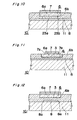
Hereinbelow, referring to Figs. 2A to 2E, a
manufacturing method for the electron source 10 of the
present invention will be described. A cross section of
only an essential portion is shown in each of Figs. 2A to
2E.
-
The electroconductive layer, which is formed of a
thin aluminum film having a predetermined film thickness,
is deposited (overlaid) on the entirety of one face (the
upper surface in Fig. 2A) of the dielectric substrate 11
according to a sputtering method. Subsequently, a resist
layer that has been patterned corresponding to a pattern
of the lower electrode 8 is formed on the
electroconductive layer. Then, unnecessary portions of
the electroconductive layer are etched using the resist
layer as a mask. Thereby, the lower electrode 8 made of
a patterned electroconductive layer is formed on the
aforementioned surface of the dielectric substrate 11.
Thereafter, the resist layer is removed. Thereby, an
intermediate product having a structure shown in Fig. 2A
is obtained.
-
Subsequently, the n-layer 21, which is formed of an
n-type polycrystalline silicon layer containing
phosphorus added as an n-type impurity, is deposited
(overlaid) on the entire portion on the side of the
aforementioned surface of the dielectric substrate 11
according to a plasma CVD method. Thereby, an
intermediate product having a structure shown in Fig. 2B
is obtained. Since the n-layer 21 is deposited according
to the plasma CVD method, the layer can be deposited by a
low-temperature process at a temperature of 600°C or
lower (100°C to 600°C). In addition, since the n-layer 21
is doped with an impurity at the layering time according
to the plasma CVD method, it can easily be formed.
-
Thereafter, the p-layer 22, which is formed of a p-type
polycrystalline silicon layer containing boron added
as a p-type impurity, is deposited by using, for example,
a plasma CVD method. Thereby, an intermediate product
having a structure shown in Fig. 2C is obtained. Since
the p-layer 22 is overlaid according to the plasma CVD
method, it can be deposited by a low-temperature process
at a temperature of 600°C or lower (100°C to 600°C). In
addition, the p-layer 22 is doped with an impurity at the
layering time according to the plasma CVD method, it can
easily be formed.
-
Subsequently, in each of the n-layer 21 and p-layer
22, oxygen ions are injected to insulate a portion
nonoverlapping with the lower electrode 8 from a portion
overlapping with the lower electrode 8. Thereafter, an
undoped polycrystalline silicon layer 3 having a
predetermined film thickness (for example, 1.5 µm) is
formed on the entire portion on the side of the
aforementioned surface of the dielectric substrate 11 by
using, for example, a plasma CVD method. Thereby, an
intermediate product having a structure shown in Fig. 2D
is obtained. Since the undoped polycrystalline silicon
layer 3 is overlaid according to the plasma CVD method,
it can be deposited by a low-temperature process at a
temperature of 600°C or lower (100°C to 600°C). The
forming method of the undoped polycrystalline silicon
layer 3 is not limited to the plasma CVD method. The
undoped polycrystalline silicon layer 3 may be deposited
using, for example, a catalytic CVD method, according to
a low-temperature process at 600°C or lower.
-
After the undoped polycrystalline silicon layer 3
has been formed, an anodic oxidation treatment is
performed at predetermined conditions. In the treatment,
an anodic oxidation process tank that contains an
electrolytic solution composed of a mixed liquid in which
a 55-wt% hydrogen fluoride aqueous solution and ethanol
are mixed at a ratio of about 1:1 is used, and light is
emitted onto the undoped polycrystalline silicon layer 3
with a platinum electrode (not shown) being set to be
cathodic and the lower electrode 8 being set to be anodic.
Thereby, a porous polycrystalline silicon layer is formed
in a portion of the polycrystalline silicon layer 3,
which overlaps with the lower electrode 8. Thereafter,
the electrolytic solution is removed from the anodic
oxidation process tank; and acid (for example,
approximately-10% dilute nitric acid, approximately-10%
dilute sulfuric acid, and aqua regia) is newly poured
into the anodic oxidation process tank. Subsequently,
the porous polycrystalline silicon layer is oxidized in a
way that the anodic oxidation process tank containing the
aforementioned acid, the platinum electrode (not shown)
is set to be cathodic, and the lower electrode 8 is set
to be anodic. Thereby, the drift portion 6a, which is
made of the oxidized porous polycrystalline silicon layer,
is formed on the portion overlapping with the lower
electrode 8. Subsequently, the surface electrode 7,
which is made of a gold film having a predetermined film
thickness (for example, 15 nm), is formed on the drift
layer 6 according to, for example, a vapor deposition
method, using a metal mask. Thereafter, the pads 27 and
28 shown in Figs. 1 are formed, and the electron source
10 shown in Fig. 3E is thereby obtained. In this
configuration, the isolating portion 6b is formed with
the polycrystalline silicon layer 3 existing in the drift
portions 6a and the portions into which the oxygen ions
have been injected.
-
During the anodic oxidation treatment in Embodiment
1, the power of the light emitted onto the surface of the
undoped polycrystalline silicon layer 3 is set at a
predetermined level, and the current density also is set
at a predetermined level. However, these conditions may
be optionally changed (for example, the current density
may be set variable). In addition, although the
electroconductive thin film used as the surface electrode
7 is formed according to a vapor deposition method, the
method of forming the electroconductive thin film is not
thereby limited, and, for example, a sputtering method
may be employed.
-
According to the above-described manufacturing
method, since the n-layer 21 and the p-layer 22 are
formed with an impurity being doped at the layering time,
the n-layer 21 and the p-layer 22 can easily be formed.
Moreover, the n-layer 21 and the p-layer 22 can
continually be deposited using the same film-depositing
apparatus (for example, a plasma CVD apparatus).
Manufacture can be easily performed for the electron
source 10 that enables the prevention of a leakage-current
flow and the implementation of a power-consumption
reduction without reducing the per-unit-area
field emission area in comparison to the conventional
cases. Furthermore, the semiconductor layers 20, the
low-concentration semiconductor layers, and the like are
made of polycrystalline silicon. In this case, since an
ordinary silicon process, a manufacturing process for a
liquid-crystal display apparatus, and the like can be
used, a cost reduction can be implemented.
(EMBODIMENT 2)
-
Hereinbelow, Embodiment 2 of the present invention
will be described. However, an electron source according
to Embodiment 2 has the same configuration as the
electron source 10 of the Embodiment 1, and only a
manufacturing method therefor is different. As such,
hereinbelow, only the manufacturing method therefor will
be described with reference to Figs. 3A to 3G. Figs. 3A
to 3G each show only a cross section of an essential
portion.
-
The electroconductive layer, which is formed of a thin
aluminum film having a predetermined film thickness, is
deposited (overlaid) on the entirety of one face (the
upper surface in Fig. 3A) of the dielectric substrate 11
according to a sputtering method. Subsequently, a resist
layer that has been patterned corresponding to a pattern
of the lower electrode 8 is formed on the
electroconductive layer. Then, unnecessary portions of
the electroconductive layer are etched using the resist
layer as a mask. Thereby, the lower electrode 8 made of
a patterned electroconductive layer is formed on the
aforementioned surface of the dielectric substrate 11.
Thereafter, the resist layer is removed. Thereby, an
intermediate product having a structure shown in Fig. 3A
is obtained.
-
Subsequently, an undoped polycrystalline silicon
layer 24 is deposited on the entire portion on the side
of the aforementioned surface of the dielectric substrate
11 according to, for example, a plasma CVD method.
Thereby, an intermediate product having a structure shown
in Fig. 3B is obtained. Since the undoped
polycrystalline silicon layer 24 is overlaid according to
the plasma CVD method, the layer can be deposited by a
low-temperature process at a temperature of 600°C or
lower (100°C to 600°C).
-
In addition, the n-layer 21 is formed while
performing doping with an n-type impurity (such as
phosphorus) according to an ion-injecting method or an
impurity-diffusing method on a portion overlapping with
the lower electrode 8 in the undoped polycrystalline
silicon layer 24. Thereby, an intermediate product
having a structure shown in Fig. 3C is obtained.
Subsequently, an undoped polycrystalline silicon layer 25
is formed on the entirety portion on the side of the
aforementioned surface of the dielectric substrate 11 by
using, for example, a plasma CVD method. Thereby, an
intermediate product shown in Fig. 3D is obtained. Since
the undoped polycrystalline silicon layer 25 is overlaid
according to the plasma CVD method, it can be deposited
by a low-temperature process at a temperature of 600°C or
lower (100°C to 600°C).
-
Thereafter, the p-layer 22 is formed while
performing doping with an p-type impurity (such as boron)
according to an ion-injecting method or an impurity-diffusing
method on a portion overlapping with the lower
electrode 8 in the undoped polycrystalline silicon layer
25. Thereby, an intermediate product having a structure
shown in Fig. 3E is obtained.
-
Subsequently, the undoped polycrystalline silicon
layer 3 having a predetermined film thickness (for
example, 1.5 µm) is formed on the entirety portion on the
side of the aforementioned surface of the dielectric
substrate 11 by using, for example, a plasma CVD method.
Thereby, an intermediate product shown in Fig. 3F is
obtained. Since the undoped polycrystalline silicon
layer 3 is overlaid according to the plasma CVD method,
it can be deposited by a low-temperature process at a
temperature of 600°C or lower (100°C to 600°C). The
forming method of the undoped polycrystalline silicon
layer 3 is not limited to the plasma CVD method. The
undoped polycrystalline silicon layer 3 may be deposited
using a different method, such as a catalytic CVD method,
according to a low-temperature process at 600°C or lower.
-
After the undoped polycrystalline silicon layer 3
has been formed, an anodic oxidation treatment is
performed at predetermined conditions. In the treatment,
an anodic oxidation process tank that contains an
electrolytic solution composed of a mixed liquid in which
a 55-wt% hydrogen fluoride aqueous solution and ethanol
are mixed at a ratio of about 1:1 is used, and light is
emitted onto the undoped'polycrystalline silicon layer 3
with a platinum electrode (not shown) being set to be
cathodic and the lower electrode 8 being set to be anodic.
Thereby, a porous polycrystalline silicon layer is formed
in a portion of the polycrystalline silicon layer 3,
which overlaps with the lower electrode 8. Thereafter,
the electrolytic solution is removed from the anodic
oxidation process tank; and acid (for example,
approximately-10% dilute nitric acid, approximately-10%
dilute sulfuric acid, and aqua regia) is newly poured
into the anodic oxidation process tank. Subsequently,
the porous polycrystalline silicon layer is oxidized in a
way that the anodic oxidation process tank containing the
aforementioned acid, the platinum electrode (not shown)
is set to be cathodic, and the lower electrode 8 is set
to be anodic. Thereby, the drift portion 6a, which is
formed of the oxidized porous polycrystalline silicon
layer, is formed on the portion overlapping with the
lower electrode 8. Subsequently, the surface electrode 7,
which is made of a gold film having a predetermined film
thickness (for example, 15 nm), is formed on th'e drift
layer 6 according to, for example, a vapor deposition
method, using a metal mask. Thereafter, the pads 27 and
28 shown in Fig. 1 are formed, and the electron source 10
shown in Fig. 3G is thereby obtained. In this
configuration, the isolating portion 6b is formed with
the polycrystalline silicon layer 3 existing in the drift
portions 6a, the undoped polycrystalline silicon layer 24,
and the undoped polycrystalline silicon layer 25 existing
in the p-layer 22.
-
In the above-described manner, in the Embodiment 2,
the respective n-layer 21 and p-layer 22 are formed while
performing doping with an impurity according to the ion-injecting
method or the impurity-diffusing method after
formation of the polycrystalline silicon layers 24 and 25,
which are undoped semiconductor layers. As such, without
depending on a film-depositing apparatus, the impurity
concentration in the n-layer 21 and the p-layer 22 can be
controlled at a high controllability.
(EMBODIMENT 3)
-
Hereinbelow, Embodiment 3 of the present invention
will be described. The basic configuration of an
electron source according to Embodiment 3 is
substantially the same as that of the electron source 10
according to Embodiment 1 shown in Fig. 1. As shown in
Fig. 4, however, the configuration is different in that
the drift portion 6a is formed on the p-layer 22. In
Embodiment 3, the semiconductor layers made of the p-layer
22 and the n-layer 21 form a leakage-current
preventing member (reverse-current preventing means).
-
Thus, in Embodiment 3, as in Embodiment 1, in
addition to the drift layer 6, the leakage-current
preventing member is provided to prevent leakage current
from flowing from the lower electrode 8 to the surface
electrode 7. Consequently, without reducing the per-unit-area
field emission area in comparison to the
conventional cases, a leakage-current flow can be
prevented, and a reduction in power consumption can be
implemented. Furthermore, the configuration is be
simplified in comparison to that of Embodiment 1 since
the undoped polycrystalline silicon layer 3 used in
Embodiment 1 is not provided between the semiconductor
layer, which forms the leakage-current preventing member,
and the drift portion 6a.
-
In comparison to the manufacturing method according.
to Embodiment 1 or Embodiment 2, a manufacturing method
for the electron source 10 of Embodiment 3 is different
only in that the entire portion overlapping with the
lower electrode 8 is formed porous according to the
anodic oxidation treatment.
(EMBODIMENT 4)
-
Hereinbelow, Embodiment 4 of the present invention
will be described. The basic configuration of an
electron source according to Embodiment 4 is
substantially the same as that of the electron source 10
according to Embodiment 1 shown in Fig. 1. As shown in
Fig. 5, however, the configuration is different in that a
silicon substrate 1, which is a semiconductor substrate,
is used for the substrate; and the lower electrode 8 in
Embodiment 1 is formed of the n-layer 21, which is formed
of an n-type silicon region having a relatively high
concentration, the p-layer 22, which is formed of a p-type
silicon region having a relatively high
concentration. In Embodiment 4, the lower electrode
formed of the p-layer 22 and the n-layer 21 forms a
leakage-current preventing member that prevents a leakage
current from flowing to the surface electrode 7 from the
lower electrode.
-
Thus, in Embodiment 4, as in Embodiment 1, in
addition to the drift layer 6, the leakage-current
preventing member is provided to prevent leakage current
from flowing to the surface electrode 7 from the lower
electrode. Consequently, without reducing the per-unit-area
field emission area in comparison to the
conventional cases, a leakage-current flow can be
prevented, and a reduction in power consumption can be
implemented.
-
In the electron source 10 according to Embodiment 4,
since the silicon substrate 1 is used for the substrate,
an ordinary silicon process, such as an ion-injecting
method or an impurity-diffusing method, can be used to
form the n-layer 21 and the p-layer 22 that form the
lower electrode. Because of the configuration, the
pattern precision of the lower electrode can be improved,
and furthermore, no nonuniform portions irregular portion,.
which can be formed with the formation of the lower
electrode, are formed on the aforementioned surface of
the substrate. Consequently, discontinuation in the
surface electrode 7 can be prevented, and the display
precision can be easily improved.
(EMBODIMENT 5)
-
Hereinbelow, Embodiment 5 of the present invention
will be described. The basic configuration of an
electron source according to Embodiment 5 is
substantially the same as that of the electron source 10
according to Embodiment 1 shown in Fig. 1. As shown in
Fig. 6, however, the configuration is different in that
an i-layer 23 formed a low-concentration polycrystalline
silicon layer is interposed between the p-layer 22 and
the n-layer 21. That is, in Embodiment 5, the
semiconductor layer formed of the p-layer 22, the i-layer
23, and the n-layer 21 form a leakage-current preventing
member that prevents a leakage current from flowing to
the surface electrode 7 from the lower electrode 8.
-
Thus, in Embodiment 5, as in Embodiment 1, in
addition to the drift layer 6, the leakage-current
preventing member is provided to prevent leakage current
from flowing to the surface electrode 7 from the lower
electrode 8. Consequently, without reducing the per-unit-area
field emission area in comparison to the
conventional cases, a leakage-current flow can be
prevented, and a reduction in power consumption can be
implemented. In addition, the semiconductor layer that
forms the leakage-current preventing member has a pin
junction. As such, compared to Embodiment 1 having the
pn junctions, the pressure resistance of the leakage-current
preventing member can be improved. The i-layer
23 may be provided between the p-layer 22 and the n-layer
21 of each of the other embodiments.
-
A manufacturing method for the electron source 10 of
Embodiment 5 is substantially the same as that in either
Embodiment 1 or Embodiment 2. The manufacturing method
is different only in that a step of forming the i-layer
23 is added; therefore, detailed description thereof is
omitted herefrom.
(EMBODIMENT 6)
-
Hereinbelow, Embodiment 6 of the present invention
will be described. The basic configuration of an
electron source according to Embodiment 6 is
substantially the same as that of the electron source 10
according to Embodiment 1 shown in Fig. 1. As shown in
Fig. 7, however, the configuration is made to be
different such that, instead of providing the
semiconductor layer 20, a material for forming a Schottky
junction in a portion interfacing with the drift portion
6a is used as a material of the surface electrode 7, and
a leakage-current preventing member is configured of the
surface electrode 7 and the drift portion 6a. For the
material of the surface electrode 7, for example, Cu, Pd,
Ag, Al, Ti, Mn, Pb, Bi, Ni, Cr, Fe, Mg, Pt, Be, Sn, Ba,
In, Co, Sb, IrSi, PtSi, Pt2Si, MnSi, Pb2Si, Co2Si, NiSi,
Ni2Si, or WSi may be used.
-
Thus, in Embodiment 6, in addition to the drift
layer 6, the leakage-current preventing member is
provided between the surface electrode 7 and the lower
electrode 8 to prevent leakage current from flowing to
the surface electrode 7 from the lower electrode 8.
Consequently, without reducing the per-unit-area field
emission area in comparison to the conventional cases, a
leakage-current flow can be prevented, and a reduction in
power consumption can be implemented. In addition, in
comparison to Embodiments 1 to 5, the configuration can
be simplified since a rectification property of the
Schottky junction between the surface electrode 7 and the
drift layer 6 can be used to prevent a leakage-current
flow, avoiding the needs for additionally providing a
junction such as the pn junction or the pin junction.
(EMBODIMENT 7)
-
Hereinbelow, Embodiment 7 of the present invention
will be described. The basic configuration of an
electron source 10 according to Embodiment 7 is
substantially the same as that of the electron source 10
according to Embodiment 6 shown in Fig. 7. However, the
configuration is made to be different such that a
material for forming a Schottky junction in a portion
interfacing with the undoped polycrystalline silicon
layer 3 is used as a material of the lower electrode 8,
and a leakage-current preventing member is configured of
the lower electrode 8 and the undoped polycrystalline
silicon layer 3. For the material of the lower electrode
8, for example, Cu, Pd, Ag, Al, Ti, Mn, Pb, Bi, Ni, Cr,
Fe, Mg, Pt, Be, Sn, Ba, In, Co, Sb, IrSi, PtSi, Pt2Si,
MnSi, Pb2Si, CO2Si, NiSi, Ni2Si, or WSi may be used.
-
Thus, in Embodiment 7, in addition to the drift
layer 6, the leakage-current preventing member is
provided between the surface electrode 7 and the lower
electrode 8 to prevent leakage current from flowing to
the surface electrode 7 from the lower electrode 8.
Consequently, without reducing the per-unit-area field
emission area in comparison to the conventional cases, a
leakage-current flow can be prevented, and a reduction in
power consumption can be implemented. In addition, in
comparison to Embodiments 1 to 5, the configuration can
be simplified since a rectification property of the
Schottky junction between the lower electrode 8 and the
undoped polycrystalline silicon layer 3 can be used to
prevent a leakage-current flow, avoiding needs for
additionally providing a junction such as a pn junction
or a pin junction.
(EMBODIMENT 8)
-
Hereinbelow, Embodiment 8 of the present invention
will be described. The basic configuration of an
electron source 10 according to Embodiment 8 is
substantially the same as that of the conventional
electron source 10" shown in Fig. 46. However, the
following aspects are different.
-
In specific, as shown in Fig. 8, an
electroconductive layer 8 (lower electrode) made of a
thin metal film (such as a thin tungsten film) is formed
on one surface of a dielectric substrate 11, and a drift
layer 6 is formed on the electroconductive layer 8, in
which the drift layer 6 includes a drift portion 6a
formed of an oxidized porous polycrystalline silicon
layer, and isolating portion 6b that is formed of a
polycrystalline silicon layer and that is formed around
the drift portions 6a. A surface electrode 7 made of a
thin metal film (such as a gold film) is formed on the
drift layer 6. The drift layer 6 is formed such that
after an undoped polycrystalline silicon layer is
overlaid on the entire portion on the side of the surface
of the dielectric substrate 11 on which the lower
electrode 8 is formed, a portion of the polycrystalline
silicon layer which corresponds to the drift portion 6a
is formed porous according to an anodic oxidation
treatment to thereby form a porous polycrystalline
silicon layer; and the porous polycrystalline silicon
layer is oxidized by using, for example, a rapid thermal
technique. The thickness of the electroconductive layer
8 is set to 200 nm, the thickness of the drift layer 6 is
set to 1.5 µm, the thickness of the drift portion 6a is
set to 1.0 µm, and the film thickness of the surface
electrode 7 is set to 15 nm. However, these numerical
values are examples; that is, the thicknesses are not
limited thereto. In Embodiment 8, the dielectric
substrate 11 forms the substrate.
-
In the drift layer 6 of the electron source 10
according to Embodiment 8, when forming the drift portion
6a, the undoped polycrystalline silicon layer is made
porous from the side of the surface in the depth
direction, and the porous formation is terminated on a
way so that the porous portion does not reach the
electroconductive layer 8. As such, a semiconductor
layer 3 formed of a portion of the polycrystalline
silicon layer is interposed between the drift portion 6a
and the electroconductive layer 8. However, the undoped
polycrystalline silicon layer may be formed porous from
the side of the surface thereof in the depth direction up
to a portion reaching the electroconductive layer 8, and
the drift portion 6a may be formed on the
electroconductive layer 8 without the semiconductor layer
3 being interposed.
-
The basic performance of the electron source 10
according to Embodiment 8 is substantially the same as
that of the conventional electron source 10" shown in
Figs. 46 and 47; hence, a detailed description thereof is
omitted herefrom. In addition, the electron emission
process is substantially the same as in the cases of the
conventional electron sources 10' and 10" (refer to Fig.
45); hence, a detailed description thereof is omitted
herefrom.
-
In Embodiment 8, the drift portion 6a is formed of
the oxidized porous polycrystalline silicon layer.
However, the drift portion 6a may be formed of a nitrided
porous polycrystalline silicon layer. Alternatively, the
drift portion 6a may be formed of an oxidized or nitrided
porous semiconductor layer, which is different from the
porous polycrystalline silicon layer. When the drift
portion 6a is formed of a nitrided porous polycrystalline
silicon layer, a silicon nitride film is formed for
either the silicon oxide film 52 or 64 shown in the Fig.
45.
-
The electron source 10 of Embodiment 8 is
characterized in that insulator films 16 are each
interposed between a vicinity of a boundary to the
isolating portion 6b in the drift portion 6a and the
surface electrode 7. Specifically, in the drift portion
6a, while the surface electrode 7 is overlaid in a
central portion, the insulator films 16 each formed in
the vicinity of the boundary to the isolating portion 6b.
In this particular case, the insulator films 16 are
formed of a silicon oxide film. However, the material of
the insulator film 16 is not limited to the silicon oxide
film. For example, the insulator film 16 may be formed
of a silicon nitride film.
-
As above, in the electron source 10 of Embodiment 8,
since the insulator film 16 is interposed between the
vicinity of the boundary to the isolating portion 6b in
the drift portion 6a and the surface electrode 7, the
field intensity in the aforementioned vicinity of the
boundary becomes sufficiently lower than the field
intensity in the central portion of the drift portion 6a.
As such, most electrons drifting in the drift portion 6a
are led to pass through the central portion of the drift
portion 6a, thereby enabling excessive electrons to be
prevented from being emitted through the aforementioned
vicinity of the boundary. Moreover, since the field
intensity in the aforementioned vicinity of the boundary
becomes lower than the field intensity in the central
portion, dielectric breakdown that can occur in the
aforementioned vicinity of the boundary can be prevented,
and an overcurrent can be prevented from locally flowing
between the electroconductive layer 8 and the surface
electrode 7. Furthermore, in the electron source 10 of
Embodiment 8, as in the conventional electron source 10'
shown in Fig. 43, the dependency to the degree of vacuum
as an electron emission property is reduced.
Concurrently, a popping phenomenon does not occur during
electron emission, and electrons can stably be emitted at
high electron emission efficiency.
-
In Embodiment 8, the insulator film 16 forms a
field-moderating member (field-moderating means) that
reduces the field intensity in the vicinity of the
boundary to the isolating portion 6b to be lower than the
field intensity in the central portion of the drift
portion 6a. Specifically, the field-moderating member is
formed of the insulator film 16 interposed between the
aforementioned vicinity of the boundary and the surface
electrode 7. As such, when a matrix structure is
employed in which a plurality of the surface electrodes 7
and a plurality of the electroconductive layers 8 are
arranged in directions intersecting with each other,
portions between individual pairs of the adjacent surface
electrodes 7 can be insulated by the insulator films 16.
(EMBODIMENT 9)
-
Hereinbelow, Embodiment 9 of the present invention
will be described. The basic configuration of an
electron source 10 according to Embodiment 9 is
substantially the same as that of the conventional
electron source 10" shown in Fig. 46. However, the
following aspects are different.
-
In specific; as shown in Fig. 9, an
electroconductive layer 8 made of a thin metal film (such
as a thin tungsten film) is formed on one surface of a
dielectric substrate 11, and insulator films 17 each made
of a silicon oxide film patterned to have a predetermined
shape are formed on the electroconductive layer 8. A
drift layer 6 is formed on the side of the surface of the
dielectric substrate 11 on which the electroconductive
layer 8 and the insulator films 17 are formed, in which
the drift layer 6 includes a drift portion 6a formed of
an oxidized porous polycrystalline silicon layer, and
isolating portion 6b that is formed of a polycrystalline
silicon layer and that is formed around the drift
portions 6a. A surface electrode 7 made of a thin metal
film (such as a gold film) is formed on the drift layer 6.
The drift layer 6 is formed such that after an undoped
polycrystalline silicon layer is overlaid on the entire
portion on the side of the surface of the dielectric
substrate 11 on which the lower electrode 8 and the
insulator films 17 are formed, a portion of the
polycrystalline silicon layer which corresponds to the
drift portion 6a is formed porous according to an anodic
oxidation treatment to thereby form a porous
polycrystalline silicon layer; and the porous
polycrystalline silicon layer is oxidized by using, for
example, a rapid thermal technique. The thickness of the
electroconductive layer 8 is set to 200 nm, the thickness
of thickness of the drift layer 6 is set to 1.5 µm, the
thickness of the drift portion 6a is set to 1.0 µm; and
the film thickness of the surface electrode 7 is set to
15 nm. However, these numerical values are examples;
that is, the thicknesses are not limited thereto. In
Embodiment 9, the dielectric substrate 11 forms the
substrate.
-
In the drift layer 6 of the electron source 10
according to Embodiment 9, when forming the drift portion
6a, the undoped polycrystalline silicon layer is made
porous from the side of the surface in the depth
direction, and the porous formation is terminated on a
way so that the porous portion does not reach the
electroconductive layer 8. As such, a semiconductor
layer 3 formed of a portion of the polycrystalline
silicon layer is interposed between the drift portion 6a
and the electroconductive layer 8. However, the undoped
polycrystalline silicon layer may be formed porous from
the side of the surface thereof in the depth direction up
to a portion reaching the electroconductive layer 8, and
the drift portion 6a may be formed on the
electroconductive layer 8 without the semiconductor layer
3 being interposed.
-
The basic performance of the electron source 10
according to Embodiment 9 is substantially the same as
that of the conventional electron source 10" shown in
Figs. 46 and 47; hence, a detailed description thereof is
omitted herefrom. In addition, the electron emission
process is substantially the same as in the cases of the
conventional electron sources 10' and 10" (refer to Fig.
45); hence, a detailed description thereof is omitted
herefrom.
-
In Embodiment 9, the drift portion 6a is formed of.
the oxidized porous polycrystalline silicon layer.
However, the drift portion 6a may be formed of a nitrided
porous polycrystalline silicon layer. Alternatively, the
drift portion 6a may be formed of an oxidized or nitrided
porous semiconductor layer, which is different from the
porous polycrystalline silicon layer. When the drift
portion 6a is formed of a nitrided porous polycrystalline
silicon layer, a silicon nitride film is formed for
either the silicon oxide film 52 or 64 shown in the Fig.
45.
-
The electron source 10 of Embodiment 9 is
characterized in that the insulator films 17 are each
interposed between a vicinity of the boundary to the
isolating portion 6b in the drift portion 6a and the
electroconductive layer 8. Specifically, in the drift
portion 6a, while only the semiconductor layer 3 is
interposed between portions interfacing with the
electroconductive layer 8 in a central portion thereof,
the semiconductor layer 3 and the insulator films 17 are
interposed in the vicinity of the boundary. In
Embodiment 9, the insulator films 17 are formed of a
silicon oxide film. However, the material of the
insulator film 17 is not limited to the silicon oxide
film. For example, the insulator film 17 may be formed
of a silicon nitride film.
-
As above, in the electron source 10 of Embodiment 9,
since the insulator film 17 is each interposed between
the vicinity of the boundary to the isolating portion 6b
in the drift portion 6a and the electroconductive layer 8,
the field intensity in the aforementioned vicinity of the
boundary becomes sufficiently lower than the field
intensity in the central portion of the drift portion 6a.
As such, most electrons drifting in the drift portion 6a
are led to pass through the central portion of the drift
portion 6a. Consequently, excessive electrons can be
prevented from being emitted through the aforementioned
vicinity of the boundary. Moreover, since the field
intensity in the aforementioned vicinity of the boundary
becomes lower than the field intensity in the central
portion, dielectric breakdown that can occur in the
aforementioned vicinity of the boundary can be prevented,
and an overcurrent can be prevented from locally flowing
between the electroconductive layer 8 and the surface
electrode 7. Furthermore, in the electron source 10 of
Embodiment 9, as in the conventional electron source 10'
shown in Fig. 43, the dependency to the degree of vacuum
as an electron emission property is reduced.
Concurrently, a popping phenomenon does not occur during
electron emission, and electrons can stably be emitted at
high electron emission efficiency.
-
In Embodiment 9, the insulator film 17 forms a
field-moderating member (field-moderating means) that
reduces the field intensity in the vicinity of the
boundary to the isolating portion 6b to be lower than the
field intensity in the central portion of the drift
portion 6a. Specifically, the field-moderating member is
formed of the insulator film 17 interposed between the
aforementioned vicinity of the boundary and the surface
electrode 7. As such, when a matrix structure is
employed in which a plurality of the surface electrodes 7
and a plurality of the electroconductive layers 8 are
arranged in directions intersecting with each other,
occurrence of crosstalk can be prevented.
(EMBODIMENT 10)
-
Hereinbelow, Embodiment 10 of the present invention
will be described. The basic configuration of an
electron source 10 according to Embodiment 10 is
substantially the same as that of the conventional
electron source 10" shown in Fig. 46. However, the
following aspects are different.
-
In specific, as shown in Fig. 10, an
electroconductive layer 8 made of a thin metal film (such
as a thin tungsten film) is formed on one surface of a
dielectric substrate 11, and a drift layer 6 is formed on
the electroconductive layer 8, in which the drift layer 6
includes a drift portion 6a formed of an oxidized porous
polycrystalline silicon layer, and isolating portion 6b
that is formed of a polycrystalline silicon layer and
that is formed around the drift portions 6a. A surface
electrode 7 made of a thin metal film (such as a gold
film) is formed on the drift layer 6. The drift layer 6
is formed such that after an undoped polycrystalline
silicon layer is overlaid on the side of the surface of
the dielectric substrate 11, a portion of the
polycrystalline silicon layer which corresponds to the
drift portion 6a is formed porous according to an anodic
oxidation treatment to thereby form a porous
polycrystalline silicon layer; and the porous
polycrystalline silicon layer is oxidized by using, for
example, a rapid thermal technique.. The thickness of the
electroconductive layer 8 is set to 200 nm, the thickness
of the drift layer 6 is set to 1.5 µm, the thickness of
the drift portion 6a is set to 1.0 µm, and the film
thickness of the surface electrode 7 is set to 15 nm.
However, these numerical values are examples; that is,
the thicknesses are not limited thereto. In Embodiment
10, the dielectric substrate 11 forms the substrate.
-
The basic performance of the electron source 10
according to Embodiment 10 is substantially the same as
that of the conventional electron source 10" shown in
Figs. 46 and 47; hence, a detailed description thereof is
omitted herefrom. In addition, the electron emission
process is substantially the same as in the cases of the
conventional electron sources 10' and 10" (refer to Fig.
45); hence, a detailed description thereof is omitted
herefrom.
-
In Embodiment 10, the drift portion 6a is formed of
the oxidized porous polycrystalline silicon layer.
However, the drift portion 6a may be formed of a nitrided
porous polycrystalline silicon layer. Alternatively, the
drift portion 6a may be formed of an oxidized or nitrided
porous semiconductor layer, which is different from the
porous polycrystalline silicon layer. When the drift
portion 6a is formed of a nitrided porous polycrystalline
silicon layer, a silicon nitride film is formed for
either the silicon oxide film 52 or 64 shown in the Fig.
45.
-
The electron source 10 of Embodiment 10 is
characterized in that a high-resistance first
semiconductor layer 23b is interposed between a vicinity
of the boundary to the isolating portion 6b in the drift
portion 6a and the electroconductive layer 8, and a low-resistance
second semiconductor layer 23a is interposed
between the central portion in the drift portion 6a and
the electroconductive layer 8. The second semiconductor
layer 23a is doped with an impurity to cause the
resistance thereof to be sufficiently lower in comparison
to that of the first semiconductor layer 23b. For
performing doping with the impurity, for example, an ion
implantation technique or a diffusion technique may be
used.
-
As above, in the electron source 10 of Embodiment 10,
the first semiconductor layer 23b is interposed between
the vicinity of the boundary to the isolating portion 6b
in the drift portion 6a and the electroconductive layer 8,
and the second semiconductor layer 23a having a
resistance sufficiently lower than that of the first
semiconductor layer 23b is interposed between the central
portion of the drift portion 6a and the electroconductive
layer 8. Accordingly, the field intensity in the
aforementioned vicinity of the boundary becomes
sufficiently lower than the field intensity in the
central portion of the drift portion 6a. Because of this
arrangement, most electrons drifting in the drift portion
6a are led to pass through the central portion of the
drift portion 6a. Consequently, excessive electrons can
be prevented from being emitted through the
aforementioned vicinity of the boundary. Moreover, since
the field intensity in the aforementioned vicinity of the
boundary becomes lower than the field intensity in the
central portion, dielectric breakdown that can occur in
the aforementioned vicinity of the boundary can be
prevented, and an overcurrent can be prevented from
locally flowing between the electroconductive layer 8 and
the surface electrode 7. In the electron source 10 of
Embodiment 10, as in the conventional electron source 10'
shown in Fig. 43, the dependency to the degree of vacuum
as an electron emission property is reduced.
Concurrently, a popping phenomenon does not occur during
electron emission, and electrons can stably be emitted at
high electron emission efficiency.
-
In Embodiment 10, the first semiconductor layer 23b
and the second semiconductor layer 23a form a field-moderating
member that reduces the field intensity in the
vicinity of the boundary to the isolating portion 6b to
be lower than the field intensity in the central portion
of the drift portion 6a. That is, since the field-moderating
member is formed of the high-resistance first
semiconductor layer 23b, which is interposed between the
aforementioned vicinity of the boundary and the
electroconductive layer 8, and the low-resistance second
semiconductor layer 23a, which is interposed between the
central portion of the drift portion 6a and the
electroconductive layer 8, restrictions for patterns of
the individual surface electrode 7 and electroconductive
layer 8 can be eliminated.
(EMBODIMENT 11)
-
Hereinbelow, Embodiment 11 of the present invention
will be described. The basic configuration of an
electron source 10 according to Embodiment 11 is
substantially the same as that of the conventional
electron source 10" shown in Fig. 46. However, the
following aspects are different.
-
In specific, as shown in Fig. 11, an
electroconductive layer 8 made of a thin metal film (such
as a thin tungsten film) is formed on one surface of a
dielectric substrate 11, and a drift layer 6 is formed on
the electroconductive layer 8, in which the drift layer 6
includes a drift portion 6a formed of an oxidized porous
polycrystalline silicon layer, and isolating portion 6b
that is formed of a polycrystalline silicon layer and
that is formed around the drift portions 6a. A surface
electrode 7 made of a thin metal film (such as a gold
film) is formed on the drift layer 6. The drift layer 6
is formed such that after an undoped polycrystalline
silicon layer is overlaid on the side of the surface of
the dielectric substrate 11 on which the
electroconductive layer 8 is formed, a portion of the
polycrystalline silicon layer which corresponds to the
drift portion 6a is formed porous according to an anodic
oxidation treatment to thereby form a porous
polycrystalline silicon layer; and the porous
polycrystalline silicon layer is oxidized by using, for
example, a rapid thermal technique. The thickness of the
electroconductive layer 8 is set to 200 nm, the thickness
of the drift layer 6 is set to 1.5 µm, the thickness of
the drift portion 6a is set to 1.0 µm, and the film
thickness of the surface electrode 7 is set to 15 nm.
However, these numerical values are examples; that is,
the thicknesses are not limited thereto. In Embodiment
11, the dielectric substrate 11 forms the substrate.
-
In the drift layer 6 of the electron source 10
according to Embodiment 11, when forming the drift
portion 6a, the undoped polycrystalline silicon layer is
made porous from the side of the surface in the depth
direction, and the porous formation is terminated on a
way so that the porous portion does not reach the
electroconductive layer 8. As such, a semiconductor
layer 3 formed of a portion of the polycrystalline
silicon layer is interposed between the drift portion 6a
and the electroconductive layer 8. However, the undoped
polycrystalline silicon layer may be formed porous from
the side of the surface thereof in the depth direction up
to a portion reaching the electroconductive layer 8, and
the drift portion 6a may be formed on the
electroconductive layer 8 without the semiconductor layer
3 being interposed.
-
The basic performance of the electron source 10
according to Embodiment 11 is substantially the same as
that of the conventional electron source 10" shown in
Figs. 46 and 47; hence, a detailed description thereof is
omitted herefrom. In addition, the electron emission
process is substantially the same as in the cases of the
conventional electron sources 10' and 10" (refer to Fig.
45); hence, a detailed description thereof is omitted
herefrom.
-
In Embodiment 11, the drift portion 6a is formed of
the oxidized porous polycrystalline silicon layer.
However, the drift portion 6a may be formed of a nitrided
porous polycrystalline silicon layer. Alternatively, the
drift portion 6a may be formed of an oxidized or nitrided
porous semiconductor layer, which is different from the
porous polycrystalline silicon layer. When the drift
portion 6a is formed of a nitrided porous polycrystalline
silicon layer, a silicon nitride film is formed for
either the silicon oxide film 52 or 64 shown in the Fig.
45.
-
The electron source 10 of Embodiment 11 is
characterized in that, cutout portions 7a are each formed
in the surface electrode 7 in a region of the drift
portion 6a which overlaps with the vicinity of the
boundary to the isolating portion 6b. That is, in the
drift portion 6a, while the surface electrode 7 is
overlaid in a central portion, the surface electrode 7
does not exist in the aforementioned vicinity of the
boundary. Specifically, in the left-right direction in
Fig. 11, the width of the surface electrode 7 is smaller
than the width of the drift portion 6a, and two ends of
the surface electrode 7 are positioned more inwardly than
two ends of the drift portion 6a.
-
As above, in the electron source 10 of Embodiment 11,
the cutout portion 7a is formed in the surface electrode
7 in the region overlapping with the vicinity of the
boundary to the isolating portion 6b. Accordingly, the
field intensity in the aforementioned vicinity of the
boundary becomes sufficiently lower than the field
intensity in the central portion of the drift portion 6a.
Because of this arrangement, most electrons drifting in
the drift portion 6a are led to pass through the central
portion of the drift portion 6a. Consequently, excessive
electrons can be prevented from being emitted through the
aforementioned vicinity of the boundary. Moreover, since
the field intensity in the aforementioned vicinity of the
boundary becomes lower than the field intensity in the
central portion, dielectric breakdown that can occur in
the aforementioned vicinity of the boundary can be
prevented, and an overcurrent can be prevented from
locally flowing between the electroconductive layer 8 and
the surface electrode 7. In the electron source 10 of
Embodiment 11, as in the conventional electron source 10'
shown in Fig. 43, the dependency to the degree of vacuum
as an electron emission property is reduced.
Concurrently, a popping phenomenon does not occur during
electron emission, and electrons can stably be emitted at
high electron emission efficiency.
-
In Embodiment 11, the cutout portion 7a in the
surface electrode 7 forms a field-moderating member that
reduces the field intensity in the vicinity of the
boundary to the isolatingportion 6b to be lower than the
field intensity in the central portion of the drift
portion 6a. Consequently, excessive electrons can be
prevented from being emitted only by changing the pattern
of the surface electrode 7 (i.e., only by changing a mask
for patterning the surface electrode 7).
(EMBODIMENT 12)
-
Hereinbelow, Embodiment 12 of the present invention
will be described. The basic configuration of an
electron source 10 according to Embodiment 12 is
substantially the same as that of the conventional
electron source 10" shown in Fig. 46. However, the
following aspects are different.
-
In specific, as shown in Fig. 12, an
electroconductive layer 8 made of a thin metal film (such
as a thin tungsten film) is formed on one surface of a
dielectric substrate 11, and a drift layer 6 is formed on
the electroconductive layer 8, in which the drift layer 6
includes a drift portion 6a formed of an oxidized porous
polycrystalline silicon layer, and isolating portion 6b
that is formed of a polycrystalline silicon layer and
that is formed around the drift portions 6a. A surface
electrode 7 made of a thin metal film (such as a gold
film) and patterned to have a predetermined shape is
formed on the drift layer 6. The drift layer 6 is formed
such that after an undoped polycrystalline silicon layer
is overlaid on the side of the surface of the dielectric
substrate 11 on which the electroconductive layer 8 is
formed, a portion of the polycrystalline silicon layer
which corresponds to the drift portion 6a is formed
porous according to an anodic oxidation treatment to
thereby form a porous polycrystalline silicon layer; and
the porous polycrystalline silicon layer is oxidized by
using, for example, a rapid thermal technique. The
thickness of the electroconductive layer 8 is set to 200
nm, the thickness of the drift layer 6 is set to 1.5 µm,
the thickness of the drift portion 6a is set to 1.0 µm,
and the film thickness of the surface electrode 7 is set
to 15 nm. However, these numerical values are examples;
that is, the thicknesses are not limited thereto. In
Embodiment 12, the dielectric substrate 11 forms the
substrate.
-
In the drift layer 6 of the electron source 10
according to Embodiment 12, when forming the drift
portion 6a, the undoped polycrystalline silicon layer is
made porous from the side of the surface in the depth
direction, and the porous formation is terminated on a
way so that the porous portion does not reach the
electroconductive layer 8. As such, a semiconductor
layer 3 formed of a portion of the polycrystalline
silicon layer is interposed between the drift portion 6a
and the electroconductive layer 8. However, the undoped
polycrystalline silicon layer may be formed porous from
the side of the surface thereof in the depth direction up
to a portion reaching the electroconductive layer 8, and
the drift portion 6a may be formed on the
electroconductive layer 8 without the semiconductor layer
3 being interposed.
-
The basic performance of the electron source 10
according to Embodiment 12 is substantially the same as
that of the conventional electron source 10" shown in
Figs. 46 and 47; hence, a detailed description thereof is
omitted herefrom. In addition, the electron emission
process is substantially the same as in the cases of the
conventional electron sources 10' and 10" (refer to Fig.
45); hence, a detailed description thereof is omitted
herefrom.
-
In Embodiment 12, the drift portion 6a is formed of
the oxidized porous polycrystalline silicon layer.
However, the drift portion 6a may be formed of a nitrided
porous polycrystalline silicon layer. Alternatively, the
drift portion 6a may be formed of an oxidized or nitrided
porous semiconductor layer, which is different from the
porous polycrystalline silicon layer. When the drift
portion 6a is formed of a nitrided porous polycrystalline
silicon layer, a silicon nitride film is formed for
either the silicon oxide film 52 or 64 shown in the Fig.
45.
-
The electron source 10 of Embodiment 12 is
characterized in that, cutout portions 8c are each formed
in the surface electrode 8 in a region of the drift
portion 6a which overlaps with the vicinity of the
boundary to the isolating portion 6b. That is, while the
electroconductive layer 8 is formed in a portion
overlapping with a central portion of the drift portion
6a, the electroconductive layer 8 does not exist in the
aforementioned vicinity of the boundary. Specifically,
in the left-right direction in Fig. 12, the width of the
surface electrode 7 is smaller than the width of the
electroconductive layer 8. Concurrently, two ends of the
electroconductive layer 8 are positioned more inwardly
than two ends of the drift portion 6a.
-
As above, in the electron source 10 of Embodiment 12,
the cutout portion 8c is each formed in the
electroconductive layer 8 in the region overlapping with
the vicinity of the boundary to the isolating portion 6b.
Accordingly, the field intensity in the aforementioned
vicinity of the boundary becomes sufficiently lower than
the field intensity in the central portion of the drift
portion 6a. Because of this arrangement, most electrons
drifting in the drift portion 6a are led to pass through
the central portion of the drift portion 6a.
Consequently, excessive electrons can be prevented from
being emitted through the aforementioned vicinity of the
boundary. Moreover, since the field intensity in the
aforementioned vicinity of the boundary becomes lower
than the field intensity in the central portion,
dielectric breakdown that can occur in the aforementioned
vicinity of the boundary can be prevented, and an
overcurrent can be prevented from locally flowing between
the electroconductive layer 8 and the surface electrode 7.
In the electron source 10 of Embodiment 12, as in the
conventional electron source 10' shown in Fig. 43, the
dependency to the degree of vacuum as an electron
emission property is reduced. Concurrently, a popping
phenomenon does not occur during electron emission, and
electrons can stably be emitted at high electron emission
efficiency.
-
In Embodiment 12, the cutout portion 8c in the
electroconductive layer 8 forms a field-moderating member
that reduces the field intensity in the vicinity of the
boundary to the isolating portion 6b to be lower than the
field intensity in the central portion of the drift
portion 6a. Consequently, in Embodiment 12, excessive
electrons can be prevented from being emitted only by
changing the pattern of the electroconductive layer 8
(i.e., only by changing a mask for patterning the
electroconductive layer 8).
(EMBODIMENT 13)
-
Hereinbelow, Embodiment 13 of the present invention
will be described. The basic configuration of an
electron source 10 according to Embodiment 13 is
substantially the same as that of the conventional
electron source 10" shown in Fig. 48. However, the
following aspects are different.
-
In specific, as shown in Fig. 13, the configuration
includes a dielectric substrate 11 made of glass
substrate; a plurality of lower electrodes 8 that are
formed of an electroconductive layer and that are
arranged on one surface of the dielectric substrate 11; a
drift layer 6 including a plurality of drift portions 6a
that are formed of an oxidized porous polycrystalline
silicon layer and that are individually formed in such a
manner as to overlap with the lower electrodes 8, and a
plurality of isolating portions 6b that are formed of a
polycrystalline silicon layer and that each fill up a
space between the drift portions 6a; and a plurality of
surface electrodes 7 arranged in directions intersecting
with (perpendicular to) each other in such a manner as to
cross the drift portions 6a and the isolating portions 6b
on the drift layer 6. The lower electrodes 8 are formed
of a thin tungsten film. The surface electrodes 7 are
formed of an electroconductive thin film made of a gold
film. The thickness of the lower electrode 8 is set to
200 nm, and the thickness of the surface electrode 7 is
set to 15 nm. However, these thicknesses are not limited
to the above numerical values. The thickness of the
drift layer 6 is set to 1.5 µm; and the thickness of the
drift portion 6a is set to 1.5 µm. The thicknesses of
the drift layer 6 and the drift portion 6a are not
limited to the above numerical values. In Embodiment 13,
the dielectric substrate 11 forms the substrate.
-
In substantially the same manner as that in the
conventional electron source 10" shown in Fig. 48, in the
electron source 10 of Embodiment 13, the drift portions
6a of the drift layer 6 are sandwiched between the
plurality of lower electrodes 8 and the plurality of
surface electrodes 7. As such, when an associated set of
the surface electrode 7 and the lower electrode 8 is
appropriately selected, and voltage is applied into the
selected set, a strong field is applied only to the drift
portion 6a in the position corresponding to the
intersection of the selected surface electrode 7 and
lower electrode 8, and electrons are thereby emitted.
Specifically, as in a case where electron sources are
individually disposed at intersections in a check pattern
formed of the surface electrodes 7 and the lower
electrodes 8, when an associated set of the surface
electrode 7 and the lower electrode 8 is selected,
electrons can be emitted from a desired intersection.
The voltage to be applied between the surface electrode 7
and the lower electrode 8 is set to a range of from 10 to
20 V. Each of the surface electrodes 7 is formed as a
stripe having two end portions in a longitudinal
direction on which pads 27 are individually formed.
Similarly, each of the lower electrodes 8 is formed as a
stripe having two end portions in a longitudinal
direction on which pads 28 are individually formed.
-
The basic performance of the electron source 10
according to Embodiment 13 is substantially the same as
that of the conventional electron source 10" shown in
Figs. 46 and 47; hence, a detailed description thereof is
omitted herefrom. In addition, the electron emission
process and a microstructure of the drift layer 6 (drift
portion 6a) are substantially the same as in the cases of
the conventional electron sources 10' and 10" (refer to
Fig. 45); hence, a detailed description thereof is
omitted herefrom.
-
In Embodiment 13, the drift portion 6a is formed of
the oxidized porous polycrystalline silicon layer.
However, the drift portion 6a may be formed of a nitrided
porous polycrystalline silicon layer. Alternatively, the
drift portion 6a may be formed of an oxidized or nitrided
porous semiconductor layer, which is different from the
porous polycrystalline silicon layer. When the drift
portion 6a is formed of a nitrided porous polycrystalline
silicon layer, a silicon nitride film is formed for
either the silicon oxide film 52 or 64 shown in the Fig.
45.
-
The electron source 10 of Embodiment 13 is
characterized in that insulator films 16 are each
interposed between a vicinity of the boundary to the
isolating portion 6b in the drift portion 6a and the
surface electrode 7. Specifically, in the drift portion
6a, while the surface electrode 7 is overlaid in a
central portion thereof, the insulator films 16 each
formed in the aforementioned vicinity of the boundary.
In addition, insulator films 26 formed of a silicon oxide
film are each formed on the side of the surface of the
drift portion 6a in such a manner as to overlap with the
adjacent surface electrodes 7. In the insulator film 26,
two end portions in the longitudinal direction of the
drift portion 6a overlap with an end portion in the width
direction of each of the surface electrodes 7.
-
In Embodiment 13, the individual insulator films 16
and 26 are formed of a silicon oxide film. However, the
material is not limited to the silicon oxide films, and
the films may be formed of, for example, a silicon
nitride film.
-
As above, in the electron source 10 of Embodiment 13,
since the insulator film 16 is interposed between the
vicinity of the boundary to the isolating portion 6b in
the.drift portion 6a and the surface electrode 7, the
field intensity in the aforementioned vicinity of the
boundary becomes sufficiently lower than the field
intensity in the central portion of the drift portion 6a.
As such, most electrons drifting in the drift portion 6a
are led to pass through the central portion of the drift
portion 6a. Thereby, excessive electrons can be
prevented from being emitted through the aforementioned
vicinity of the boundary. In addition, an individual
space between the surface electrodes 7 can be insulated
by the insulator film 16. Moreover, since the insulator
films 26 made of the silicon oxide film are each formed
on the side of the surface of the drift layer 6 in such a
manner as to overlap with the adjacent surface electrodes
7, electrons can be prevented from being emitted through
portions between individual pairs of the adjacent surface
electrodes 7; and concurrently, crosstalk can be
prevented. Furthermore, since the field intensity in the
aforementioned vicinity of the boundary becomes lower
than the field intensity in the central portion,
dielectric breakdown that can occur in the aforementioned
vicinity of the boundary can be prevented, and an
overcurrent can be prevented from locally flowing between
the lower electrode 8 and the surface electrode 7. In
the electron source 10 of Embodiment 13, as in the
conventional electron source 10' shown in Fig. 43, the
dependency to the degree of vacuum as an electron
emission property is reduced. Concurrently, a popping
phenomenon does not occur during electron emission, and
electrons can stably be emitted at high electron emission
efficiency.
-
In Embodiment 13, the insulator film 16 forms a
field-moderating member that reduces the field intensity
in the vicinity of the boundary to the isolating portion
6b to be lower than the field intensity in the central
portion of the drift portion 6a.
(EMBODIMENT 14)
-
Hereinbelow, Embodiment 14 of the present invention
will be described. The basic configuration of an
electron source 10 according to Embodiment 14 is
substantially the same as that of the conventional
electron source 10" shown in Fig. 48. However, the
following aspects are different.
-
In specific, as shown in Fig. 14, the configuration
includes a dielectric substrate 11 made of glass
substrate; a plurality of lower electrodes 8 that are
formed of an electroconductive layer and that are
arranged on one surface of the dielectric substrate 11; a
drift layer 6 including a plurality of drift portions 6a
that are formed of an oxidized porous polycrystalline
silicon layer and that are individually formed in such a
manner as to overlap with the lower electrodes 8, and a
plurality of isolating portions 6b that are formed of a
polycrystalline silicon layer and that each fill up a
space between the drift portions 6a; and a plurality of
surface electrodes 7 arranged in directions intersecting
with (perpendicular to) the lower electrodes 8 in such a
manner as to cross the drift portions 6a and the
isolating portions 6b on the drift layer 6. The lower
electrodes 8 are formed of a thin tungsten film. The
surface electrodes 7 are formed of an electroconductive
thin film made of a gold film. The thickness of the
lower electrode 8 is set to 200 nm, and the thickness of
the surface electrode 7 is set to 15 nm. However, these
thicknesses are not limited to the above numerical values.
The thickness of the drift layer 6 is set to 1.5 µm, and
the thickness of the drift portion 6a is set to 1.0 µm.
The thicknesses of the drift layer 6 and the drift
portion 6a are not limited to the above numerical values.
In Embodiment 14, the dielectric substrate 11 forms the.
substrate.
-
As in the conventional electron source 10" shown in
Fig. 48, in the electron source 10 of Embodiment 14, the
drift portions 6a of the drift layer 6 are sandwiched
between the plurality of lower electrodes 8 and the
plurality of surface electrodes 7. As such, when an
associated set of the surface electrode 7 and the lower
electrode 8 is appropriately selected, and voltage is
applied into the selected set, a strong field is applied
only to the drift portion 6a in the position
corresponding to the intersection of the selected surface
electrode 7 and lower electrode 8, and electrons are
thereby emitted. Specifically, as in a case where
electron sources are individually disposed at
intersections in a check pattern formed of the surface
electrodes 7 and the lower electrodes 8, when an
associated set of the surface electrode 7 and the lower
electrode 8 is selected, electrons can be emitted from a
desired intersection. The voltage to be applied between
the surface electrode 7 and the lower electrode 8 is set
to a range of from 10 to 20 V. Each of the surface
electrodes 7 is formed as a stripe having two end
portions in a longitudinal direction on which pads 27 are
individually formed. Similarly, each of the lower
electrodes 8 is formed as a stripe having two end
portions in a longitudinal direction on which pads 28 are
individually formed.
-
The basic performance of the electron source 10
according to Embodiment 14 is substantially the same as
that of the conventional electron source 10" shown in
Figs. 46 and 47; hence, a detailed description thereof is
omitted herefrom. In addition, the electron emission
process and a microstructure of the drift layer 6 (drift
portion 6a) are substantially the same as in the cases of
the conventional electron sources 10' and 10" (refer to
Fig. 45); hence, a detailed description thereof is
omitted herefrom.
-
In Embodiment 14, the drift portion 6a is formed of
the oxidized porous polycrystalline silicon layer.
However, the drift portion 6a may be formed of a nitrided
porous polycrystalline silicon layer. Alternatively, the
drift portion 6a may be formed of an oxidized or nitrided
porous semiconductor layer, which is different from the
porous polycrystalline silicon layer. When the drift
portion 6a is formed of a nitrided porous polycrystalline
silicon layer, a silicon nitride film is formed for
either the silicon oxide film 52 or 64 shown in the Fig.
45.
-
The electron source 10 of Embodiment 14 is
characterized in that the insulator films 17 are each
formed on the lower electrode 8 in the portion between
the vicinity of the boundary to the isolating portion 6b
and the electroconductive layer 8. That is, while the
central portion of the drift portion 6a is overlaid on
the electroconductive layer 8, the insulator film 17 is
formed in the aforementioned vicinity of the boundary.
In addition, insulator films 37 made of a silicon oxide
film is each formed on the drift portion 6a on the side
of the wiring 8a in such a manner as to overlap with the
adjacent surface electrodes 7. In the insulator film 37,
two end portions in the longitudinal direction of the
drift portion 6a overlap with an end portion of the
surface electrodes 7 in the width direction.
-
In Embodiment 14, the individual insulator films 17
and 37 are formed of a silicon oxide film. However, the
material is not limited to the silicon oxide films, and
the films may be formed of, for example, a silicon
nitride film.
-
As above, in the electron source 10 of Embodiment 14,
since the insulator film 16 is interposed between the
vicinity of the boundary to the isolating portion 6b in
the drift portion 6a and the electroconductive layer 8,
the field intensity in the aforementioned vicinity of the
boundary becomes sufficiently lower than the field
intensity in the central portion of the drift portion 6a.
As such, most electrons drifting in the drift portion 6a
are led to pass through the central portion of the drift
portion 6a. Thereby, excessive electrons can be
prevented from being emitted through the aforementioned
vicinity of the boundary. Moreover, since the insulator
films 37 made of the silicon oxide film are each formed
on the side of the surface of the drift layer 6 in such a
manner as to overlap with the adjacent surface electrodes
7, electrons can be prevented from being emitted through
portions between individual pairs of the adjacent surface
electrodes 7; and concurrently, crosstalk can be
prevented. Furthermore, since the field intensity in the
aforementioned vicinity of the boundary becomes lower
than the field intensity in the central portion,
dielectric breakdown that can occur in the aforementioned
vicinity of the boundary can be prevented, and an
overcurrent can be prevented from locally flowing between
the lower electrode 8 and the surface electrode 7.
Furthermore, in the electron source 10 of Embodiment 14,
as in the conventional electron source 10' shown in Fig.
43, the dependency to the degree of vacuum as an electron
emission property is reduced. Concurrently, a popping
phenomenon does not occur during electron emission, and
hence electrons can stably be emitted at high electron
emission efficiency.
-
In Embodiment 14, the insulator film 17 forms a
field-moderating member that reduces the field intensity
in the vicinity of the boundary to the isolating portion
6b to be lower than the field intensity in the central
portion of the drift portion 6a.
(EMBODIMENT 15)
-
Hereinbelow, Embodiment 15 of the present invention
will be described. The basic configuration of an
electron source 10 according to Embodiment 15 is
substantially the same as that of the conventional
electron source 10" shown in Fig. 48. However, the
following aspects are different.
-
In specific, as shown in Fig. 15, the configuration
includes a dielectric substrate 11 made of glass
substrate; a plurality of lower electrodes 8 that are
formed of an electroconductive layer and that are
arranged on one surface of the dielectric substrate 11; a
drift layer 6 including a plurality of drift portions 6a
that are formed of an oxidized porous polycrystalline
silicon layer and that are individually formed in such a
manner as to overlap with the lower electrodes 8, and a
plurality of isolating portions 6b that are formed of a
polycrystalline silicon layer and that each fill up a
space between the drift portions 6a; and a plurality of
surface electrodes 7 arranged in directions intersecting
with (perpendicular to) the lower electrodes 8 on the
drift layer 6. The drift layer 6 includes drift portions
6a that are made of an oxidized porous polycrystalline
silicon layer and that are each formed of on the side of
the surface electrodes 7 in a region where the surface
electrode 7 and the lower electrode 8 overlap with each
other; isolating portions 6b that are made of an undoped
polycrystalline silicon layer and that are each formed
between the adjacent drift portions 6a in the
longitudinal direction of the surface electrode 7; high-resistance
first semiconductor layers 23b each interposed
between the vicinity of a boundary to the isolating
portion 6a in the drift portion 6a and the lower
electrode 8; low-resistance second semiconductor layers
23b each formed between the drift portion 6a and the
lower electrode 8; and isolating portions 6c each formed
between the adjacent drift portions 6a in the
longitudinal direction of the lower electrode 8.
-
The lower electrodes 8 are formed of a thin tungsten
film. The surface electrodes 7 are formed of an
electroconductive thin film made of a gold film. The
thickness of the lower electrode 8 is set to 200 nm, and
the thickness of the surface electrode 7 is set to 15 nm.
However, these thicknesses are not limited to the above
numerical values. The thickness of the drift layer 6 is
set to 1.5 µm, and the thickness of the drift portion 6a
is set to 1.0 µm. The thicknesses of the drift layer 6
and the drift portion 6a are not limited to the above
numerical values. The dielectric substrate 11 forms the
substrate.
-
As in the conventional electron source 10" shown in
Fig. 48, in the electron source 10 of Embodiment 15, the
drift portions 6a of the drift layer 6 are sandwiched
between the plurality of lower electrodes 8 and the
plurality of surface electrodes 7. As such, when an
associated set of the surface electrode 7 and the lower
electrode 8 is appropriately selected, and voltage is
applied into the selected set, a strong field is applied
only to the drift portion 6a in the position
corresponding to the intersection of the selected surface
electrode 7 and lower electrode 8, and electrons are
thereby emitted. Specifically, as in a case where
electron sources are individually disposed at
intersections in a check pattern formed of the surface
electrodes 7 and the lower electrodes 8, when an
associated set of the surface electrode 7 and the lower
electrode 8 is selected, electrons can be emitted from a
desired intersection. The voltage to be applied between
the surface electrode 7 and the lower electrode 8 is set
to a range of from 10 to 20 V. Each of the surface
electrodes 7 is formed as a stripe having two end
portions in a longitudinal direction on which pads 27 are
individually formed. Similarly, each of the lower
electrodes 8 is formed as a stripe having two end
portions in a longitudinal direction on which pads 28 are
individually formed.
-
The basic performance of the electron source 10
according to Embodiment 15 is substantially the same as
that of the conventional electron source 10" shown in
Figs. 46 and 47; hence, a detailed description thereof is
omitted herefrom. In addition, the electron emission
process and a microstructure of the drift layer 6 (drift
portion 6a) are substantially the same as in the cases of
the conventional electron sources 10' and 10" (refer to
Fig. 45); hence, a detailed description thereof is
omitted herefrom.
-
In Embodiment 15, the drift portion 6a is formed of
the oxidized porous polycrystalline silicon layer.
However, the drift portion 6a may be formed of a nitrided
porous polycrystalline silicon layer. Alternatively, the
drift portion 6a may be formed of an oxidized or nitrided
porous semiconductor layer, which is different from the
porous polycrystalline silicon layer. When the drift
portion 6a is formed of a nitrided porous polycrystalline
silicon layer, a silicon nitride film is formed for
either the silicon oxide film 52 or 64 shown in the Fig.
45.
-
The electron source 10 of Embodiment 15 is
characterized in that the high-resistance first
semiconductor layers 23b are each formed between the
vicinity of the boundary to the isolating portion 6b in
the drift portion 6a and the electroconductive layer 8,
and the second semiconductor layers 23a having a
resistance that is sufficiently lower than that of the
first semiconductor layer 23b are each interposed between
the central portion of the drift portion 6a and the lower
electrode 8.
-
As above, in the electron source 10 of Embodiment 15,
the high-resistance first semiconductor layers 23b are
each formed between the vicinity of the boundary to the
isolating portion 6b and the electroconductive layer 8,
and the second semiconductor layers 23a having a
resistance that is sufficiently lower than that of the
first semiconductor layer 23b are each interposed between
the central portion of the drift portion 6a and the lower
electrode 8. Accordingly, the field intensity in the
aforementioned vicinity of the boundary becomes
sufficiently lower than the field intensity in the
central portion of the drift portion 6a. As such, most
electrons drifting in the drift portion 6a are led to
pass through the central portion of the drift portion 6a.
Thereby, excessive electrons can be prevented from being
emitted through the aforementioned vicinity of the
boundary. Moreover, since portions between the adjacent
drift portions 6a are insulated by the isolating portions
6b or the isolating portions 6c, electrons can be
prevented from being emitted through portions between
individual pairs of the adjacent surface electrodes 7;
and concurrently, crosstalk can be prevented.
Furthermore, since the field intensity in the
aforementioned vicinity of the boundary becomes lower
than the field intensity in the central portion,
dielectric breakdown that can occur in the aforementioned
vicinity of the boundary can be prevented, and an
overcurrent can be prevented from locally flowing between
the lower electrode 8 and the surface electrode 7.
Furthermore, in the electron source 10 of Embodiment 15,
as in the conventional electron source 10' shown in Fig.
43, the dependency to the degree of vacuum as an electron
emission property is reduced. Concurrently, a popping
phenomenon does not occur during electron emission, and
hence electrons can stably be emitted at high electron
emission efficiency.
-
In Embodiment 15, the first semiconductor layer 23b
and the second semiconductor layer 23a form a field-moderating
member that reduces the field intensity in the
vicinity of the boundary to the isolating portion 6b to
be lower than the field intensity in the central portion
of the drift portion 6a. That is, since the field-moderating
member is formed of the high-resistance first
semiconductor layer 23b, which is interposed between the
aforementioned vicinity of the boundary and the lower
electrode 8, and low-resistance second semiconductor
layer 23a, which is interposed between the central
portion of the drift portion 6a, restrictions for
patterns of the individual surface electrode 7 and
electroconductive layer 8 can be eliminated.
-
In Embodiments 8 to 15, the gold film is used for
the electroconductive thin film for forming the surface
electrodes 7. However, the material for the surface
electrode 7 is not limited to gold. As described in
Embodiment 1, the material having a small work function,
such as aluminum, chrome, tungsten, nickel, or platinum,
may be used. The important matters and advantages in
using these materials are as described in Embodiment 1.
-
In Embodiments 8 to 15, the thin tungsten film is
used for the lower electrodes 8 (electroconductive
layers). However, the material is not limited to
tungsten. Instead of tungsten, any one of aluminum,
nickel, cobalt, chrome, hafnium, molybdenum, palladium,
platinum, rhodium, tantalum, titanium, and zirconium.
Moreover, materials that may be used include an oxide of
one of the aforementioned metal materials, an alloy
composed of a plurality of materials selected from the
aforementioned metal materials, or an alloy composed of
Si and selected materials from the aforementioned
materials (for example, an aluminum-based Ai―Si alloy).
-
The lower electrodes 8 may be formed of an
electroconductive layer composed of a plurality of
electroconductive layers laminated in the thickness
direction. In this case, aluminum is preferably used for
an electroconductive film formed as the top layer; and
copper, which has a low resistance in comparison to
aluminum, is preferably used for an electroconductive
film as the bottom layer.
(EMBODIMENT 16)
-
Hereinbelow, Embodiment 16 of the present invention
will be described.
-
Figs. 16A and 16B are schematic cross-sectional
views each showing an electron source 10 according to
Embodiment 16 of the present invention. Figs. 17A to 17D
each show a cross section of an electron source 10 in a
primary step of manufacturing the electron source 10, or
an intermediate product thereof during the manufacture
thereof. For an electroconductive substrate, Embodiment
16 uses a monocrystalline n-type silicon substrate 1 that
has a resistivity that is relatively close to a conductor
resistivity (for example, a (100) substrate of which
resistivity is about 0.01 Ωcm to 0.02 Ωcm).
-
A basic configuration of the electron source 10
according to Embodiment 16 is substantially the same as
that of the conventional electron source 10' shown in Fig.
43. Specifically, as shown in Fig. 16A, a drift layer 6
made of an oxidized porous polycrystalline silicon layer
is formed on a main surface of the n-type silicon
substrate 1. A field moderating layer 9 made of a
silicon nitride film is formed on the drift layer 6. A
surface electrode 7 made of an electroconductive thin
film (for example, a gold film) is formed on the field
moderating layer 9. An ohmic electrode 2 is formed on a
reverse surface of the n-type silicon substrate 1. As
described above, in Embodiment 16, the drift layer 6 is
formed on the main surface of the n-type silicon
substrate 1. However, an undoped polycrystailine silicon
layer may be formed between the main surface of the n-type
silicon substrate 1 and the drift layer 6.
-
Also in the electron source 10 of Embodiment 16,
electrons can be emitted according to operational
principles similar to those for the conventional electron
source 10' shown in Figs. 43 and 44. In specific, as
shown in Fig. 18, similarly to the conventional case, a
direct-current voltage Vps is applied between the surface
electrode 7 and the n-type silicon substrate 1; and
concurrently, a direct-current voltage Vc is applied
between a collector electrode 12 and the surface
electrode 7. With the individual direct-current voltages
Vps and Vc being appropriately set, electrons injected
from the n-type silicon substrate 1 are led to drift
through a drift layer 6, and are led to be emitted
through the field moderating layer 9 and the surface
electrode 7 (Single dotted lines in Fig. 16 each
represent the flow of electrons e-emitted through the
surface electrode 7). A material having a small work
function is used for the surface electrode 7, and the
film thickness of the surface electrode 7 is set to about
1 to 15 nm.
-
In specific, as shown in Fig. 16B, as in the
conventional electron source 10' shown in Fig. 45, a
drift portion 6a includes grain 51 made of columner
polycrystalline silicon; a thin silicon oxide film 52
formed on one surface of the grain 51; fine silicon
crystal 63 on the order of nanometer that is interposed
between items of the grain 51; and a silicon oxide film
64 that is formed on one surface of the fine silicon
crystal 63 and that has a film thickness smaller than a
crystal grain diameter of the fine silicon crystal 63.
It is considered that, in the drift layer 6, the surface
of grain included in a polycrystalline silicon layer 3
(refer to Figs. 17A to 17D) prior to an anodic oxidation
treatment described below becomes porous, and the crystal
condition is maintained with the residual grain 51. As
such, a most part of the field applied to the drift layer
6 is caused to intensively pass through the silicon oxide
film 64 accelerated by a strong field applied on the
silicon oxide film 64, the injected electrons e- are
accelerated by the strong field between the items of
grain 51, and are thereby caused to drift upward as
viewed in Fig. 16B. Electrons that have reached the
surface of the drift layer 6 are hot electrons that
easily pass through the surface electrode 7 and that are
emitted into a vacuum.
-
In the electron source 10, the higher the ratio
(Ie/Ips) of an emitted electron current Ie with respect
to a diode current Ips, the higher the electron emission
efficiency. In the electron source 10, electrons can be
emitted even when the direct-current voltage Vps to be
applied between the surface electrode 7 and the ohmic
electrode 2 is in a low range of from 10 to 20 V. In the
electron source 10, the dependency to degree of vacuum as
an electron emission property is reduced. Moreover, no
popping phenomenon occurs, hence electrons can be stably
emitted at a high electron emission efficiency.
-
The electron source 10 of Embodiment 16 is
characterized in that the field moderating layer 9 is
provided between the drift layer 6 and the surface
electrode 7 for moderating the field intensity of the
drift layer 6 in a state where the direct-current voltage
Vps (driving voltage) is applied. Since the field
moderating layer 9 is interposed between the drift layer
6 and the surface electrode 7, the field moderating layer
9 is preferably formed of a material not allowing easy
diffusion of electrons, and the film thickness thereof is
preferably small sufficient to cause electrons drifted
through the drift layer 6 to reach the surface electrode
7 without substantially being diffused. When the
resistance value of the field moderating layer 9 is one
digit or smaller than the resistance value of the drift
layer 6, effects of moderating the field intensity of the
drift layer 6 decrease. When the resistance value of the
field moderating layer 9 is greater than the resistance
value of the drift layer 6, the driving voltage needs to
be increased. As such, the resistance value of the field
moderating layer 9 is preferably on the same order as the
resistance value of the drift layer 6. In the Embodiment
16, the thickness of the drift layer 6 is set to 1.5 µm,
and the film thickness of the field moderating layer 9 is
set to 50 nm. However, the film thickness of the field
moderating layer 9 is not limited to 50 nm, and the film
thickness may be appropriately set within a range of from
10 nm to 100 nm corresponding to the resistance value of
the drift layer 6. While the resistance value of the
drift layer 6 varies depending on the thickness of the
drift layer 6 and the driving voltage, the values are
ranged from several tens kΩ to several tens MΩ.
-
In the electron source 10 of Embodiment 16, since
the field moderating layer 9 for moderating the field
intensity of the drift layer 6 is provided between the
drift layer 6 and the surface electrode 7, a reduction
can be implemented for the field intensity in a portion
where dielectric breakdown tends to occur in either the
silicon oxide film 52 or 64, dielectric breakdown in the
aforementioned portion can be prevented, and ageing
variations in the diode current Ips and the emitted
electron current Ie can be minimized. Consequently, the
ageing stability in the electron emission properties such
as electron emission efficiency can be improved; and when
the above is applied to, for example, a display, a
gradual reduction in the screen luminance can be
prevented. With the field moderating layer 9 being
provided, the intensity of a field to be applied to the
drift layer 6 is reduced. For this reason, when the
driving voltage (direct-current voltage Vps) to be
applied between the surface electrode 7 and the n-type
silicon substrate 1 (ohmic electrode 2) formed of the
electroconductive substrate is controlled to be the same
as that in the conventional electron source 10' not
including the field moderating layer 9, the emitted
electron current Ie is reduced smaller than that in the
case where the field moderating layer 9 is not provided.
However, by increasing the driving voltage, the level of
the emitted electron current Ie can be increased to
become equivalent to that in the conventional electron
source 10'.
-
In the electron source 10 of Embodiment 16, the
field moderating layer 9 is formed of the silicon nitride
film. Since the silicon nitride film a high resistivity,
the film thickness of the field moderating layer 9 may be
reduced. In addition, since the silicon nitride film has
a high electron transmittance, and it does not allow easy
diffusion of electrons that has drifted through the drift
layer 6, the reduction in electron emission efficiency
according to the provision of the field moderating layer
9 can be inhibited.
In Embodiment 16, the n-type silicon substrate 1 is
used for the electroconductive substrate. The
electroconductive substrate is provided to form the
cathode of the electron source 10, to support the drift
layer 6 in the vacuum, and to inject electrons into the
drift layer 6. As such, the electroconductive substrate
may be only to be appropriate to form the cathode of the
electron source 10 and to support the drift layer 6. As
such, the electroconductive substrate is not limited to
the n-type silicon substrate, and it may instead be a
metal substrate made of, for example, a chrome material.
Alternatively, as shown in Fig. 46, the electroconductive
substrate may be a substrate having the lower electrode 8
formed on the side of one surface (the side of the main
surface) of the dielectric substrate 11 formed of, for
example, glass. With the glass substrate having one
surface on which the lower electrode 8 is formed, area-enlargement
and cost reduction can be implemented for the
electron source in comparison to a configuration using a
semiconductor substrate.
-
In Embodiment 16, a gold film is used as the
electroconductive thin film that forms the surface
electrodes 7. However, the material of the surface
electrode 7 is not limited to the gold material. As
described in Embodiment 1, a different material having a
small work function, such as aluminum, chrome, tungsten,
nickel, or platinum, may be used. Matters to be noted
and advantages in using the materials are as described in
Embodiment 1.
-
In Embodiment 16, the drift layer 6 is formed of the
oxidized porous polycrystalline silicon layer. However,
the drift portion 6 may instead be formed of a nitrided
porous polycrystalline silicon layer. Alternatively, the
drift portion 6 may be formed of an oxidized or nitrided
porous semiconductor layer, which is different from the
porous polycrystalline silicon layer. When the drift
portion 6 is formed of a nitrided porous polycrystalline
silicon layer, a silicon nitride film is formed for
either the silicon oxide film 52 or 64 shown in the Fig.
16B. In addition, in Embodiment 16, the field moderating
layer 9 is formed of the silicon nitride film. However,
the field moderating layer 9 may instead be formed of,
for example, an oxidized silicon film, amolphous silicon,
amolphous carbonized silicon, a metal oxide film, or a
metal nitride film, which has a low electron diffusion
property and a high resistivity.
-
Hereinbelow, referring to Figs. 17A to 17D, a
manufacturing method for the electron source 10 shown in
Figs. 16A and 16B will be described.
-
First, the ohmic electrode 2 is formed on a reverse
surface of the n-type silicon substrate 1. Then, the
undoped polycrystalline silicon layer (polycrystalline
silicon thin film) 3 having a predetermined film
thickness (for example, 1.5 µm) is deposited (overlaid)
on the main surface of the n-type silicon substrate 1
according to, for example, an LPCVD method. Thereby, an
intermediate product having a structure shown in Fig. 17A
is obtained.
-
Subsequently, an anodic oxidation treatment is
performed at predetermined conditions such that an anodic
oxidation process tank that contains an electrolytic
solution composed of a mixed liquid in which a 55-wt%
hydrogen fluoride aqueous solution and ethanol are mixed
at a ratio of about 1:1 is used, and light is emitted
onto the polycrystalline silicon layer 3 with a platinum
electrode (not shown) being set to be cathodic and the n-type
silicon substrate 1 (ohmic electrode 2) being set to
be anodic. Thereby, a porous polycrystalline silicon
layer 4 is formed, and an intermediate product having a
structure shown in Fig. 17B is obtained. Conditions of
the anodic oxidation treatment are as follows. A surface
of the polycrystalline silicon layer 3 is set to be in
contact with the electrolytic solution, the current
density is fixed at 30 mA/cm2, and the electroconduction
time is set to 10 seconds. For an optical source of
emitting light onto the polycrystalline silicon layer 3,
a 500W tungsten lamp is used. In Embodiment 16, the
polycrystalline silicon layer 3 is formed porous to reach
the n-type silicon substrate 1 in the depth direction.
However, it may be formed porous up to a midway point in
the depth direction. In this case, a portion of the
polycrystalline silicon layer 3 remains between the n-type
silicon substrate 1 and the porous polycrystalline
silicon layer 4.
-
After completion of the anodic oxidation treatment,
a rapid thermal oxidation technique using a rapid thermal
technique is used to perform rapid thermal oxidation for
the porous polycrystalline silicon layer 4. This forms
the drift layer 6 made of the oxidized porous
polycrystalline silicon layer. Thereafter, the field
moderating layer 9 having a predetermined film thickness
(for example, 50 nm) is formed on the drift layer 6
according to a sputtering method; and thereby, an
intermediate product having a structure shown in Fig. 17C
is obtained. The rapid thermal oxidation is performed
using a lamp annealing device. The flow rate of oxygen
gas is set to 0.3 L/min (300 sccm) in a standard
condition. In Embodiment 16, since oxidation is
performed for the porous polycrystalline silicon layer 4
according to the rapid thermal oxidation, the temperature
can be raised up to an oxidation temperature within
several seconds, thereby enabling the inhibition of
entailed oxidation that can occur as a problem with an
ordinary oxidizing device of a furnace core pipe type
when materials are fed into the furnace.
-
The field moderating layer 9 is formed according to
the sputtering method in the following steps. Nitride
silicon is used as a target, and a chamber is evacuated
up to a level of 1 × 10⁻⁴ Pa or lower in a standard
condition. Then, an Ar gas is introduced into the
chamber at a flow rate of 0.03 L/min (30 sccm) in a
standard condition, and the pressure in the chamber is
thereby adjusted to 5 × 10⁻¹ Pa. Thereafter, a high
frequency power of 1 W/cm2 is fed between electrodes
arranged in the chamber, and a silicon nitride film is
formed.
-
After the field moderating layer 9 has been formed,
a gold film used as the surface electrode 7 is formed
according to, for example, a vapor deposition method; and
thereby, the electron source 10, as shown in Fig. 17B, is
obtained.
-
In the manufacture employing the above-described
manufacturing method, the electron source 10 having a
high ageing stability can be obtained only by adding a
step of overlaying the field moderating layer 9 on the
drift layer 6 to the manufacturing method for the
conventional electron source 10'.
-
The electron source 10 manufactured according to the
above-described manufacturing method has a less
dependency to the degree of vacuum as an electron
emission property. Concurrently, since no popping
phenomenon occurs, electrons can be stably emitted.
Moreover, for the semiconductor substrate, such as a
polycrystalline silicon substrate, used for the
electroconductive substrate, since a substrate formed of,
for example, a glass substrate on which an
electroconductive layer (such as an ITO film) is formed,
can be used; as such, in comparison to the Spindt-type
electrode, electron source area can be enlarged and costs
can be reduced.
-
When the electroconductive substrate is formed of a
semiconductor substrate, the polycrystalline silicon
layer 3 may be formed according to a sputtering method
instead of the LPCVD method. Alternatively, the film
deposition may be performed such that amolphous silicon
is deposited according to a plasma CVD method, and
thereafter, the film is crystallized. When the
electroconductive substrate is formed of a glass
substrate on which an electroconductive layer is formed,
the polycrystalline silicon layer 3 may be formed such
that amolphous silicon is deposited on the
electroconductive layer according to a CVD method, and
the silicon layer is annealed. The method for forming
the polycrystalline silicon layer 3 on the
electroconductive layer is not limited to the CVD method.
For example, a CGS (continuous grain silicon) method or a
catalytic CVD method process may instead be employed.
-
For an oxidation method for the porous
polycrystalline silicon layer 4, electrochemical
oxidation using acid (for example, dilute sulfuric acid,
dilute nitric acid, or aqua regia) may be employed
instead of the thermal oxidation method. Before the
porous polycrystalline silicon layer 4 is
electrochemically oxidized with acid, a treatment may be
performed such that the layer is immersed in an oxidant
solution (such as nitric acid, sulfuric acid,
hydrochloric acid, or hydrogen peroxide water) for a time
necessary to allow a polar surface of the porous
polycrystalline silicon layer 4 to be oxidized; and
thereby, hydrogen atoms terminating silicon atoms are
substituted with oxygen atoms. Alternatively, oxidation
may be performed such that ultraviolet rays are emitted
onto the layer in a gas phenomenon containing at least
one of oxygen and ozone. Still alternatively, oxidation
may be performed such that the layer is exposed to plasma
in a gas phenomenon containing at least one of oxygen and
ozone. Still alternatively, oxidation may be performed
such that the layer is heated in a gas phenomenon
containing at least one of oxygen and ozone (the heat
temperature may be appropriately set within a temperature
range of from 100°C to 600°C). Still alternatively,
oxidation may be performed such that ultraviolet rays are
emitted onto the layer, and the layer is heated (the heat
temperature may be appropriately set within a temperature
range of from 100°C to 600°C). Still alternatively,
oxidation may be performed such that, in a gas phenomenon
containing at least one of oxygen and ozone, ultraviolet
rays are emitted onto the layer, and the layer is heated
(the heat temperature may be appropriately set within a
temperature range of from 100°C to 600°C). Further
alternatively, oxidation may be performed employing
combined methods of the above. Yet alternatively,
oxidation may be performed employing methods that are
different from the above oxidation methods. In
consequence, the diffusion amount of impurities into
either the silicon oxide film 52 or 64 is reduced, and
the dielectric strength is improved. The porous
polycrystalline silicon layer 4 is thus oxidized, but it
may instead be nitrided.
-
The method of forming the field moderating layer 9
is not limited to the sputtering method, and a different
method such as a vapor deposition method or an ion
plating method may instead be employed. Moreover, the
method of forming the surface electrode 7 is not limited
to the vapor deposition method; and a method such as a
sputtering method may instead be used.
-
Hereinbelow, a display using the electron source 10
of Embodiment 16 will be described with reference to Fig.
19.
-
As shown in FIG. 19, the display includes a glass
substrate 33 disposed opposite to the surface electrodes
7 of the electron source 10. Collector electrodes 31 are
arranged in a striped state on a surface of the glass
substrate 33, which opposes the electron source 10. A
phosphor layer 32 that emits visible light according to
electron beams emitted through the surface electrodes 7
is disposed in such a manner as to cover the collector
electrodes 31. The surface electrodes 7 are formed in a
striped state. A spacing between the electron source 10
and the glass substrate 33 is maintained in a vacuum
state.
-
In the display, the surface electrode 7 is formed as
a stripe, and the collector electrodes 31 also is formed
as a stripe to extend perpendicular to the surface
electrode 7. When one of the collector electrodes 31 and
one of the surface electrodes 17 are selected, and
voltage (field) is applied thereto, electrons are emitted
only from the surface electrode 7 to which the voltage is
applied. In the surface electrode 7 from which the
electrons have been emitted, only electrons emitted from
a region thereof through which the voltage has been
applied to the corresponding collector electrode 31 are
accelerated, and the accelerated electrons cause the
phosphor layer 32 covering the collector electrode 31 to
emit light.
-
In short, in the display shown in Fig. 19, when
voltage is applied to specific one of the surface
electrodes 7 and specific one of the collector electrodes
31, a portion corresponding to a region where the two
electrodes 7 and 31 mutually intersect can be caused to
emit light. As such, by optionally changing the surface
electrodes 7 and the collector electrodes 31 to which
voltage is to be applied, images or characters can be
displayed on the display. In the display, a high voltage
needs to be applied to the collector electrode 31 and to
thereby accelerate electrons in order to cause phosphors
of the phosphor layer 32 according to electrons emitted
from the electron source 10. To achieve the above, a
high voltage of hundreds of V or several kV may be
applied to the collector electrode 31.
(EMBODIMENT 17)
-
Hereinbelow, Embodiment 17 of the present invention
will be described.
-
As shown in Fig. 20, while the basic configuration
of an electron source 10 according to Embodiment 17 is
substantially the same as that of the electron source 10
according to Embodiment 16, it is characterized in that
the field moderating layer 9 is configured to include a
silicon nitride film 9a formed on the drift layer 6, and
a silicon oxide film 9b formed on the silicon nitride
film 9a. Essentially, in Embodiment 16, the field
moderating layer 9 is formed of a multilayer film
including the silicon nitride film 9a, and the surface
electrode 7 is overlaid on the silicon oxide film 9b.
Either the silicon nitride film 9a or the silicon oxide
film 9b is formed according to a sputtering method.
-
As described above, also in Embodiment 17, basically,
the same advantages as those in Embodiment 16 can be
obtained. However, in Embodiment 17, since the
resistivity of each of the silicon nitride film 9a and
the silicon oxide film 9b is high, the film thickness of
the field moderating layer 9 can be reduced. In addition,
electrons drifted through the drift layer 6 are not
allowed to easily diffuse in the silicon nitride film 9a,
a reduction in electron emission efficiency according to
the provision of the field moderating layer 9 can be
inhibited. Moreover, in Embodiment 17, since the surface
electrode 7 is formed on the oxide nitride film 9a, in
comparison to a case as in Embodiment 16 where the
surface electrode 7 is formed on the field moderating
layer 9 made of the silicon nitride film, the electron
movement to the surface electrode 7 easily occurs,
thereby enabling the electron emission efficiency to
increase.
-
The film thickness of the silicon nitride film 9a is
set to 40 nm, and the film thickness of the silicon oxide
film 9b is set to 10 nm. These film thicknesses are not
limited to the aforementioned numerical values, and the
film thicknesses may be appropriately set corresponding
to, for example, the thickness and the resistance value
of the drift layer 6. However, since electrons less
diffuse in the silicon nitride film 9a than in the
silicon oxide film 9b, the film thickness of the silicon
nitride film 9a is preferably set larger than that of the
silicon oxide film 9b.
(EMBODIMENT 18)
-
Hereinbelow, Embodiment 18 of the present invention
will be described.
-
As shown in Fig. 21, while the basic configuration
of an electron source 10 according to Embodiment 18 is
substantially the same as that of the electron source 10
according to Embodiment 16, it is characterized in that
the field moderating layer 9 is configured to include a
first silicon oxide film 9c formed on the drift layer 6,
a silicon nitride film 9a formed on the silicon oxide
film 9c, and a second silicon oxide film 9b formed on the
silicon nitride film 9a. Essentially, in Embodiment 18,
the field moderating layer 9 is formed of a multilayer
film including the silicon nitride film 9a, and the
surface electrode 7 is overlaid on the silicon oxide film
9b. Each of the silicon nitride film 9a and the silicon
oxide films 9c and 9b is formed according to a sputtering
method.
-
As described above, also in Embodiment 18, basically,
effects similar to those in Embodiment 16 can be obtained.
However, in Embodiment 18, since the resistivity of each
of the silicon nitride film 9a and the silicon oxide
films 9c and 9b is high, the film thickness of the field
moderating layer 9 can be reduced. In addition,
electrons drifted through the drift layer 6 are not
allowed to easily diffuse in the silicon nitride film 9a,
a reduction in electron emission efficiency according to
the provision of the field moderating layer 9 can be
inhibited. Moreover, in Embodiment 18, since the surface
electrode 7 is formed on the second silicon oxide film 9a,
in comparison to a case as in Embodiment 16 where the
surface electrode 7 is formed on the field moderating
layer 9 made of the silicon nitride film, the electron
movement to the surface electrode 7 easily occurs,
thereby enabling the electron emission efficiency to
increase.
-
The film thickness of the first silicon oxide film
9c is set to 10 nm, and the film thickness of the second
silicon oxide film 9b is set to 40 nm. These film
thicknesses are not limited to the aforementioned
numerical values, and the film thicknesses may be
appropriately set corresponding to, for example, the
thickness and the resistance value of the drift layer 6.
However, since electrons less diffuse in the silicon
nitride film 9a than in each of the silicon oxide films
9c and 9b, the film thickness of the silicon nitride film
9a is preferably set larger than that of each of the
silicon oxide films 9c and 9b.
(EMBODIMENT 19)
-
Hereinbelow, Embodiment 19 of the present invention
will be described. Basically, the basic configuration of
an electron source 10 according to Embodiment 19 is
substantially the same as that of the electron source 10
according to Embodiment 16, it is characterized in that
the field moderating layer 9 of the electron source 10
according to Embodiment 16 shown in Figs. 16A and 16B is
configured of to include a chrome oxide film. Since
chrome oxide film is a material that has a high property
of adhesion to the surface electrode 7 at least to an
extent not causing the surface electrode 7 to be isolated,
it can inhibit ageing deterioration that can because of
isolation of the surface electrode 7 from the field
moderating layer 9 and ageing variations in electron
emission property. In addition, since the chrome oxide
film has a high transmittance property, it can inhibit a
reduction in electron emission efficiency, which can
occur because of the provision of the field moderating
layer 9. Consequently, also in the electron source 10 of
Embodiment 19, the same advantages as those in Embodiment
16 can be obtained.
-
Hereinbelow, a manufacturing method for the electron
source 10 of Embodiment 19 will be described with
reference to Figs. 22A to 22D. The manufacturing method
is substantially the same as the manufacturing method for
the electron source 10 of Embodiment 16. As such,
hereinbelow, descriptions of aspects, common to those
given in Embodiment 16 will be simplified to avoid
repetitive description.
-
In Embodiment 19, after the ohmic electrode 2 has
been formed on a reverse surface of the n-type silicon
substrate 1, that is, the electroconductive substrate,
the undoped polycrystalline silicon layer 3 is formed on
one surface of the n-type silicon substrate 1 according
to an LPCVD method, and an intermediate product having a
structure shown in Fig. 22B is obtained. Subsequently,
the polycrystalline silicon layer 3 is formed porous
according to an anodic oxidation treatment, the porous
polycrystalline silicon layer 4 is thereby formed, and an
intermediate product having a structure shown in Fig. 22B
is obtained.
-
In addition, the porous polycrystalline silicon
layer 4 is thermally oxidized, and the drift layer 6 made
of the oxidized porous polycrystalline silicon layer is
thereby formed. Then, an oxidized layer 19 made of a
chrome layer is formed on the drift layer 6 according to
an electron beam vapor deposition method. Moreover, the
surface electrode 7 made of a gold metal is formed on the
oxidized layer 19, and an intermediate product having a
structure shown in Fig. 22C is obtained. In Embodiment
19, the film thickness of the oxidized layer 19 is set to
20 nm, and the film thickness of the surface electrode 7
is set to 15 nm. However, these film thicknesses are not
limited to the aforementioned numerical values.
-
After the surface electrode 7 has been formed, the
oxidized layer 19 is oxidized according to an oxidation
process, the field moderating layer 9 formed of an chrome
oxide film, and an electron source 10 as shown in Fig.
22D is obtained. The oxidation process may be carried
out by introducing, for example, ozone generated using an
ozone generator into an oxidizing treatment chamber. In
Embodiment 19, an oxygen gas is introduced into an ozone
generator at a flow rate of 5L/min in a standard
condition, electric discharge is performed to thereby
generate 5%-concentration ozone, and the ozone is
introduced into an oxidizing treatment chamber. In the
treatment, the n-type silicon substrate 1 used for the
electroconductive substrate is heated at 150°C. In
Embodiment 19, a chrome oxide film is used to form an
oxide layer.
-
The manufacturing method includes a step of forming
the oxidized layer 19 by using chrome on the drift layer
6 formed on the side of the main surface of the n-type
silicon substrate 1 used for the electroconductive
substrate, in which the chrome is a composition element
from which oxygen is excluded from composition elements
of the field moderating layer 9; a step of forming the
surface electrode 7 on the oxidized layer 19; and a step
of forming the field moderating layer 9 by oxidizing the
oxidized layer 19 according to the oxidation process
after the surface electrode 7 has been formed. As such,
the electron source 10 having a high ageing stability can
be provided. In addition, since the field moderating
layer 9 is formed by oxidizing the oxidized layer 19
according to the oxidation process after the surface
electrode 7 has been performed, the field moderating
layer 9 can be prevented from being contaminated and
damaged during the oxidation process. Moreover, in the
oxidation process, since the oxidized layer 19 is
oxidized with ozone diffusing through the surface
electrode 7, the oxidized layer 19 can be oxidized at a
temperature that is lower than that in the thermal
oxidation. As such, the method enables the prevention of
damage causing electrical disconnection and layer
isolation attributable to coagulation of gold, which is a
composition element of the surface electrode 7.
-
In the Embodiment 19, while the oxidized layer 19 is
oxidized using ozone in the oxidation process, the
oxidized layer 19 may be oxidized using oxygen plasma.
Also in this case, the oxidized layer 19 can be oxidized
at a lower temperature than that in the thermal oxidation,
thereby enabling damage causing electrical disconnection
and layer isolation attributable to coagulation of
composition elements of the surface electrode.
(EMBODIMENT 20)
-
Hereinbelow, Embodiment 20 of the present invention
will be described.
-
As shown in Fig. 23, the basic configuration of an
electron source 10 according to Embodiment 20 is
substantially the same as that of the conventional
electron source 10" shown in Fig. 54. Specifically, it
includes a dielectric substrate 11 made of a glass
substrate; a plurality of wirings 8a (lower electrodes 8)
that are made of an electroconductive layer (for example,
a metal film, such as a chrome, or an ITO film) and that
are arranged on a main surface of the dielectric
substrate 11; a drift layer 6 composed of a plurality of
drift portions 6a formed of an oxidized porous
polycrystalline silicon layer in such a manner as to
overlap with the wirings 8a, and isolating portions 6b
that are formed of a polycrystalline silicon layer and
that individually fill up spaces between the drift
portions 6a; a plurality of surface electrodes 7 that
individually oppose the wirings 8a via the drift portions
6a; and a plurality of bus electrodes 25 commonly
coupling the plurality of surface electrode 7, which are
arranged in the direction intersecting with the wirings
8a, in units of each row on the drift layer 6. The bus
electrodes 25 are arranged in such a manner as to cross
the drift portions 6a and the isolating portions 6b in
the direction intersecting with the wirings 8a. For the
surface electrodes 7, a material (such as gold) having a
small work function is employed; and the film thickness
of the surface electrode 7 is set to a range of from 15
to 15 nm. For the bus electrodes 25, a material (such as
aluminum or copper) that has a low resistance and a high
processability is employed. Since the bus electrode 25
does not need to transmit electrons, the film thickness
thereof can be increased in comparison to that of the
surface electrode 7, thereby enabling the resistance to
be reduced. In Embodiment 20, the dielectric substrate
11 forms the substrate.
-
As shown in Figs. 23 and 24, the electron source 10
of Embodiment 20 is characterized in that narrow portions
18a made of an electroconductive are each interposed to
narrow a current passageway (to reduce the current
passage area) between the surface electrode 7 and the bus
electrode 25.
-
As shown in Fig. 25, the narrow portion 18a causes
disconnection when an overcurrent flows. Specifically,
in the narrow portion 18a, the thermal capacity is formed
to have a small thermal capacity to cause disconnection
when an overcurrent flows. In the electron source 10,
each of the surface electrodes 7 is sandwiched between
two of the bus electrodes 25 commonly coupled to
identical pads 28. Each of the narrow portions 18a is
interposed between the surface electrode 7 and the bus
electrodes 25 and 25 on two sides thereof. The narrow
portion 18a is thus interposed between the surface
electrode 7 and the bus electrode 25, and forms an
overcurrent protection element for limiting the current
flowing to the surface electrode 7.
-
In the electron source 10 of Embodiment 20, as in
the conventional electron source 10" shown in Fig. 54,
the drift portions 6a of the drift layer 6 are sandwiched
between the plurality of wirings 8a and the plurality of
the surface electrodes 7. As such, when an associated
set of the bus electrode 25 and the wiring 8a is
appropriately selected, and voltage is applied to the
selected set, a strong field is applied only to the drift
portion 6a positioned below the surface electrode 7 that
is proximate to a portion corresponding to an
intersection with the wiring 8a in the selected bus
electrode 25, and electrons are thereby emitted. That is,
when an associated set of the bus electrode 25 and the
wiring 8a to which voltage is applied, electrons can
thereby be emitted from a desired cross point. The
voltage to be applied between the bus electrode 25 and
the lower electrode 8 is set to a range of from 10 to 20
V. Each of the wirings 8a is formed as a stripe having
two end portions in a longitudinal direction on which
pads 27 are individually formed. The bus electrode 25 is
coupled to the individual pads 28 at two ends in the
longitudinal direction thereof.
-
The basic performance of the electron source 10
according to Embodiment 20 is substantially the same as
that of the conventional electron source 10" shown in
Figs. 46 and 47; hence, a detailed description thereof is
omitted herefrom. In addition, the set and a
microstructure of the drift layer 6 (drift portion 6a)
are substantially the same as in the cases of the
conventional electron sources 10' and 10" (refer to Fig.
45); hence, a detailed description thereof is omitted
herefrom.
-
In the electron source 10 of Embodiment 20, since
the narrow portions 18a are each interposed between the
surface electrode 7 and the bus electrode 25, when an
overcurrent flows to a specific one of the surface
electrodes 7, the narrow portion 18a interposed between
the surface electrode 7 and the bus electrode 25 causes
disconnection. Consequently, an overcurrent can be
prevented from continually flowing to a specific one of
the surface electrodes 7, a deterioration range can be
prevented from being increased because of heat generation,
and the reliability can be improved. Essentially, since
the overcurrent protection element for limiting current
flowing to the surface electrode 7 is interposed between
the surface electrode 7 and the bus electrode 25, an
overcurrent flowing between the bus electrode 25 and the
surface electrode 7 can be limited. Thereby, an
overcurrent flowing to the surface electrode 7, the drift
portion 6a, and the wiring 8a can be limited, and the
temperatures thereof can be inhibited from being
increased. Consequently, the deterioration range can be
prevented from being increased, and the reliability can
thereby be improved. In other words, disconnection can
be caused only in the narrow portion 18a interposed
between an overcurrent-flowed surface electrode 7 and a
bus electrode 25, in which the surface electrode 7 is one
of those corresponding to individual pixels. Thereby,
influence on the surface electrodes 7 corresponding to
other pixels can be inhibited, and the reliability as an
electron source used with a display can be improved. In
the electron source 10 of Embodiment 20, the isolating
portion 6b insulates a portion between the adjacent drift
portions 6a, thereby enabling crosstalk in which, for
example, electrons are emitted through the portion
between the adjacent drift portions 6a, to be prevented.
Moreover, in the electron source 10 of Embodiment 20, as
in the conventional electron source 10', the dependency
to the degree of vacuum as an electron emission property
is reduced. Concurrently, no popping phenomenon occurs
during electron emission, and hence electrons can stably
be emitted at high electron emission efficiency.
(EMBODIMENT 21)
-
Hereinbelow, Embodiment 21 of the present invention
will be described.
-
As shown in Figs. 26 and 27, the basic configuration
of an electron source 10 according to Embodiment 21 is
substantially the same as that of the electron source 10
according to Embodiment 20; however it is different in
that high resistance layers 18b are each interposed
between the surface electrode 7 and the bus electrode 25.
Each of the narrow portions 18a is interposed between the
surface electrode 7 and the bus electrodes 25, and forms
an overcurrent protection element for limiting the
current flowing to the surface electrode 7.
-
Thus, in comparison to the conventional electron
source 10" shown in Fig. 54 in which the individual
surface electrodes 7 and bus electrodes 25 are directly
coupled, in the electron source 10 of Embodiment 21, an
overcurrent can be prevented from flowing to the surface
electrode 7, a deterioration range can be prevented from
being increased because of heat generation, and the
reliability can be improved.
(EMBODIMENT 22)
-
Hereinbelow, Embodiment 22 of the present invention
will be described.
-
As shown in Figs. 28 to 30, the basic configuration
of an electron source 10 according to Embodiment 22 is
substantially the same as that of that in Embodiment 20;
however, it is different in that thermo-sensitive layers
18c having a positive resistance temperature coefficient
are each interposed between the surface electrode 7 and
the bus electrode 25.
-
As shown in Fig. 31, in the thermo-sensitive layer
18c, the resistance value increases according to the
increase in temperature. As a material of the thermo-sensitive
layer 18c, for example, a BaTiO3-based material
used for a PTC thermistor may be used. The thermo-sensitive
layer 18c forms an overcurrent protection
element for limiting the current flowing to the surface .
electrode 7. Other portions are the same as those in
Embodiment 20.
-
Thus, in the electron source 10 of Embodiment 22,
when an overcurrent flows to the surface electrode 7, and
the temperature increases, the.resistance of the thermo-sensitive
layer 18c interposed between the surface
electrode 7 and the bus electrode 25 increases. Thereby,
in comparison to the conventional electron source 10"
shown in Fig. 54, an overcurrent can be prevented from
flowing to the surface electrode 7. Consequently, a
deterioration range can be prevented from being increased
because of heat generation, and the reliability can be
improved.
(EMBODIMENT 23)
-
Hereinbelow, Embodiment 23 of the present invention
will be described.
-
As shown in Fig. 32, the basic configuration of an
electron source 10 according to Embodiment 23 is
substantially the same as that of the conventional
electron source 10" shown in Fig. 54. Specifically, it
includes a dielectric substrate 11 made of a glass
substrate; a plurality of wirings 8a (lower electrodes 8)
that are made of an electroconductive layer (for example,
a metal film, such as a chrome, or an ITO film) and that
are arranged on a main surface of the dielectric
substrate 11; a drift layer 6 composed of a plurality of
drift portions 6a formed of an oxidized porous
polycrystalline silicon layer in such a manner as to
overlap with the wirings 8a, and isolating portions 6b
that are formed of a polycrystalline silicon layer and
that individually fill up spaces between the drift
portions 6a; a plurality of surface electrodes 7 that
individually oppose the wirings 8a via the drift portions
6a; and a plurality of bus electrodes 25 commonly
coupling the plurality of surface electrode 7, which are
arranged in the direction intersecting with the wirings
8a, in units of each row on the drift layer 6. The bus
electrodes 25 are arranged in such a manner as to cross
the drift portions 6a and the isolating portions 6b in
the direction intersecting with the wirings 8a. For the
surface electrodes 7, a material (such as gold) having a
small work function is employed; and the film thickness
of the surface electrode 7 is set to a range of from 15
to 15 nm. For the bus electrodes 25, a material (such as
aluminum or copper) that has a low resistance and a high
processability is employed. In Embodiment 23, the
dielectric substrate 11 forms the substrate.
-
As shown in Figs. 32 and 34, the electron source 10
is characterized in that the drift portions 6a are each
formed in a rectangular-parallelepiped shape, and metal
layers 18 each covering a vicinity of a side 6c along the
longitudinal direction of the bus electrode 25 (side 6c
that is parallel to the bus electrode 25) are provided.
-
In Embodiment 23, passage of electrons can be
prevented by setting the thickness of the metal layer 7
to be larger than the mean free path of the electrons
drifting through the drift portion 6a. For a material of
the metal layer 18, for example, gold may be used. With
the gold being used, the resistance of the metal layer 18
can be reduced, and concurrently, a high property of
adhesion between the surface electrode 7 and the bus
electrode 25 can be implemented. The metal layer 18
forms an electron-emission restraining portion that
restrains electrons from being emitted through a
peripheral portion of the drift portion 6a on the drift
layer 6. In this particular case, while the gold is used
for the material of the metal layer 18, the material of
the metal layer 18 is not limited to the gold.
-
In the electron source 10 of Embodiment 23, as in
the conventional electron source 10" shown in Fig. 54,
the drift portions 6a of the drift layer 6 are sandwiched
between the plurality of wirings 8a and the plurality of
the surface electrodes 7. As such, when an associated
set of the bus electrode 25 and the wiring 8a is
appropriately selected, and voltage is applied to the
selected set, a strong field is applied only to the drift
portion 6a positioned below the surface electrode 7 that
is proximate to a portion corresponding to an
intersection with the wiring 8a in the selected bus
electrode 25, and electrons are thereby emitted. That is,
when an associated set of the bus electrode 25 and the
wiring 8a to which voltage is applied, electrons can
thereby be emitted from a desired cross point. The
voltage to be applied between the bus electrode 25 and
the lower electrode 8 is set to a range of from 10 to 20
V. Each of the wirings 8a is formed as a stripe having
two end portions in a longitudinal direction on which
pads 27 are individually formed. The bus electrode 25 is
coupled to the individual pads 28 at two ends in the
longitudinal direction thereof.
-
The basic performance of the electron source 10
according to Embodiment 23 is substantially the same as
that of the conventional electron source 10" shown in
Figs. 46 and 47; hence, a detailed description thereof is
omitted herefrom. In addition, the set and a
microstructure of the drift layer 6 (drift portion 6a)
are substantially the same as in the cases of the
conventional electron sources 10' and 10" (refer to Fig.
45); hence, a detailed description thereof is omitted
herefrom.
-
In the electron source 10 of Embodiment 23, since
the metal layers 18 each covering a vicinity of a side 6c
along the longitudinal direction of the bus electrode 25
are provided, by setting the thickness of the metal layer
18 to be larger than the mean free path of the electrons,
electrons can be prevented from being emitted through a
portion positioned below the metal layer 18 in a
peripheral portion of the drift portion 6a. Consequently,
when the electron source is adapted in a display,
occurrence of bleeding can be prevented, and a high-precision
display can be implemented. In addition, the
electron source enables occurrence of crosstalk in which,
for example, electrons is emitted through a portion
between the adjacent drift portions 6a, to be prevented.
In the electron source 10 of Embodiment 23, as in the
conventional electron source 10', the dependency to the
degree of vacuum as an electron emission property is
reduced. Concurrently, no popping phenomenon occurs
during electron emission, and hence electrons can stably
be emitted at high electron emission efficiency.
(EMBODIMENT 24)
-
Hereinbelow, Embodiment 24 of the present invention
will be described.
-
As shown in Figs. 35 and 36, while the basic
configuration of an electron source 10 according to
Embodiment 24 is substantially the same as that of the
electron source 10 shown in Fig. 23, it is different in
that a metal layer 18 covers the entire peripheral
portion of the drift portion 6a. Specifically, in
Embodiment 24, the metal layer 18 is formed as a
rectangular frame in such a manner as to cover all the
vicinities of sides 6c and 6c, which each extend parallel
to the bus electrode 25, and sides 6d and 6d, which each
extend perpendicular to the bus electrode 25. The metal
layer 18 forms an electron-emission restraining portion
that restrains electrons from being emitted through a
peripheral portion of the drift portion 6a on the drift
layer 6. Other portions are the same as those in
Embodiment 23; hence, descriptions thereof are omitted
herefrom.
-
Thus, as in the electron source 10 of Embodiment 23,
in the electron source 10 of Embodiment 24, by setting
the thickness of the metal layer 18 to be larger than the
mean free path of the electrons, electrons can be
prevented from being emitted through a portion positioned
below the metal layer 18 in a peripheral portion of the
drift portion 6a. Consequently, when the electron source
is used in a display, occurrence of bleeding can be
prevented, and a high-precision display can be
implemented. In the electron source 10 of Embodiment 24,
since field emission can be prevented in the overall
peripheral portion of the drift portion 6a, in comparison
to Embodiment 23, a higher-precision display can be
implemented. In a display using the electron source 10
of Embodiment 23, when the pixel size is reduced to
further improve the precision, because of influences of
electrons emitted from two sides of the drift portion 6a
in the direction along which the wirings 8a are arranged,
bleeding develops to an extent that cannot be ignored.
However, in the electron source 10 of Embodiment 24,
since the metal layer 18 also covers vicinities of the
sides 6d of the drift portion 6a, which each extend along
the longitudinal direction of the wiring 8a, electrons
emission from two end portions of the drift portion 6a in
the direction along which the wirings 8a are arranged can
be prevented, and the display precision can be improved
even higher.
(EMBODIMENT 25)
-
Hereinbelow, Embodiment 25 of the present invention
will be described.
-
As shown in Figs. 37 and 38, while the basic
configuration of an electron source 10 according to
Embodiment 25 is substantially the same as that of the
electron source 10 shown in Fig. 23, it is different in
that the bus electrode 25 is formed to have portions that
each overlap with the side 6c of the drift portion 6a,
which extends in the longitudinal direction of the bus
electrode 25, and an end portion of the surface electrode
7. In Embodiment 25, while the metal layer 18 in
Embodiment 23 (refer to Fig. 32) is not provided, the
electron-emission restraining portion in Embodiment 23 is
formed of the portion of the bus electrode 25. Since the
bus electrode 25 does not need to transmit electrons, the
thickness thereof can be set larger than the mean free
path of electrons that drift through the drift portion 6a.
Other portions are the same as those in Embodiment 23;
hence, descriptions thereof are omitted herefrom.
-
Thus, in the electron source 10 of Embodiment 25,
since the electron-emission restraining portion is formed
of the portion of the bus electrode 25, by setting the
thickness of the bus electrode 25 to be larger than the
mean free path of the electrons, electrons can be
prevented from being emitted because of the bus electrode
25 through a peripheral portion of the drift portion 6a.
Consequently, when the electron source is used in a
display, occurrence of bleeding can be prevented, and a
high-precision display can be implemented. In comparison
to the electron source 10 of Embodiment 24 in which the
lower electrodes 8 are provided, in the electron source
10 of Embodiment 25, no portion overlapping with the
metal layer 18 is required. Consequently, the field
emission areas of the individual surface electrodes 7 are
maintained equal, the dimensions of the surface electrode
7 can be reduced, and the pixel size can thereby be
reduced.
(EMBODIMENT 26)
-
Hereinbelow, Embodiment 26 of the present invention
will be described.
-
As shown in Fig. 39, an electron source 10 according
to Embodiment 26 includes a dielectric substrate 11 made
of a glass substrate; a plurality of wirings 8a that are
made of an electroconductive layer (for example, a metal
film, such as a chrome, or an ITO film) and that are
arranged on a main surface of the dielectric substrate
11; a drift layer 6 composed of a plurality of drift
portions 6a formed of an oxidized porous polycrystalline
silicon layer in such a manner as to overlap with the
wirings 8a, and isolating portions 6b that are formed of
a polycrystalline silicon layer and that individually
fill up spaces between the drift portions 6a; a plurality
of surface electrodes 7 arranged to oppose the wirings 8a
via the drift portions 6a in the direction intersecting
with the wirings 8a and in the direction along which the
lower electrodes 8 extend; and a plurality of bus
electrodes 25 commonly coupling the plurality of surface
electrode 7, which are arranged in the direction
intersecting with the wirings 8a, in units of each row on
the drift layer 6. Each of the wirings 8a is formed as a
stripe having two end portions in a longitudinal
direction on which pads 27 are individually formed. The
bus electrode 25 is coupled to the individual pads 28 at
two ends in the longitudinal direction thereof.
-
The surface electrodes 7 are formed of a material
(such as gold) having a small work function; and the film
thickness of the surface electrode 7 is set to a range of
from 15 to 15 nm. The bus electrodes 25 are formed of a
material (such as aluminum or copper) that has a low
resistance and a high processability is employed. Since
the bus electrode 25 does not need to transmit electrons,
the film thickness thereof can be increased in comparison
to that of the surface electrode 7, thereby enabling the
resistance to be reduced. The dielectric substrate 11
forms the substrate.
-
In the electron source 10 of Embodiment 26, as in
the conventional electron source 10" shown in Fig. 54,
the drift portions 6a of the drift layer 6 are sandwiched
between the plurality of wirings 8a and the plurality of
the surface electrodes 7. As such, when an associated
set of the bus electrode 25 and the wiring 8a is
appropriately selected, and voltage is applied to the
selected set, a strong field is applied only to the drift
portion 6a positioned below the surface electrode 7 that
is proximate to a portion corresponding to an
intersection with the wiring 8a in the selected bus
electrode 25, and electrons are thereby emitted. That is,
when an associated set of the bus electrode 25 and the
wiring 8a to which voltage is applied, electrons can
thereby be emitted from a desired cross point. The
voltage to be applied between the bus electrode 25 and
the lower electrode 8 is set to a range of from 10 to 20
V.
-
The basic performance of the electron source 10
according to Embodiment 26 is substantially the same as
that of the conventional electron source 10" shown in
Figs. 46 and 47; hence, a detailed description thereof is
omitted herefrom. In addition, the set and a
microstructure of the drift layer 6 (drift portion 6a)
are substantially the same as in the cases of the
conventional electron sources 10' and 10" (refer to Fig.
45); hence, a detailed description thereof is omitted
herefrom.
-
In the conventional electron source 10" shown in Fig.
54, the drift portions 6a are arranged in the direction
along which the wirings 8a extend, and the isolating
portions 6b are interposed between the adjacent drift
portions 6a. In comparison to the above, the electron
source 10 of Embodiment 26 is characterized in that the
drift portions 6a are continually formed in the direction
along which the lower electrodes 8a extend. In specific,
the drift portion 6a formed to overlap with the wiring 8a
is disposed to extend in the direction along which the
wiring 8a extends, and the adjacent wirings 8a the'
adjacent drift portions 6a are isolated by the isolating
portion 6b in the direction intersecting with the wiring
8a.
-
In Embodiment 26, since the drift portion 6a is
continually formed in the direction along which the
wiring 8a extends, the distance between the surface
electrodes 7 that are arranged adjacent to each other in
the direction along which the wiring 8a extends can be
reduced, as shown in Fig. 40, in comparison to the case
where the drift portions 6a and the isolating portions 6b
are alternately formed as in the conventional electron
source 10" shown in Fig. 54. As such, in comparison to a
case where the conventional electron source 10" is used
as an electron source in a display, the interpixel
distance on the side of the faceplate can be reduced, and
the electron source can be used as an electron source in
a high-precision display. In addition, as in the
conventional electron source 10', in the electron source
10 of Embodiment 26, the dependency to the degree of
vacuum as an electron emission property is reduced.
Concurrently, no popping phenomenon occurs during
electron emission, and hence electrons can stably be
emitted at high electron emission efficiency.
(EMBODIMENT 27)
-
Hereinbelow, Embodiment 27 of the present invention
will be described.
-
As shown in Fig. 41, while the basic configuration
of an electron source 10 according to Embodiment 27 is
substantially the same as that of the electron source 10
of Embodiment 26, it is different in that each of the
surface electrodes 7 is sandwiched between two bus
electrodes 25 commonly connected to the identical pads 28.
In specific, in Embodiment 27, each of the surface
electrodes 7 is coupled to the individual bus electrodes
25 at two ends thereof in the direction (right-left
direction in Fig. 42) along which the wiring 8a extends.
The thickness of the bus electrode 25 is set larger than
the mean free path of electrons. Other aspects are the
same as those in Embodiment 26; hence, descriptions
thereof are omitted herefrom.
-
As in Embodiment 26, in Embodiment 27, the drift
portion 6a is continually formed in the direction along
which the wiring 8a extends. As such, the distance
between the surface electrodes 7 that are arranged
adjacent to each other in the direction along which the
wiring 8a extends can be reduced, as shown in Fig. 42, in
comparison to, for example, the conventional electron
source 10" shown in Fig. 54, in which the drift portions
6a and the isolating portions 6b are alternately formed.
As such, in comparison to a case where the conventional
electron source 10" is used as an electron source in a
display, the interpixel distance on the side of the
faceplate can be reduced, and the electron source can be
used as an electron source in a high-precision display.
In addition, electrons can be prevented from being
emitted through the drift portion 6a positioned below the
bus electrode 25, and the area in a portion through which
electrons are emitted can be prevented from being larger
than the surface area of the surface electrode 7.
-
For the electroconductive layer, Embodiments 20 to
27 use the substrate formed such that the lower
electrodes 8 are formed on the side of one surface of the
dielectric substrate 11 made of the glass substrate.
However, a metal substrate made of, for example, chrome,
may be used for the electroconductive substrate.
Alternatively, a semiconductor substrate (such as an n-type
silicon substrate of which the resistivity is
relatively close to the conductor resistivity, or a p-type
silicon substrate on which an n-type region is
formed as an electroconductive layer on the side of one
surface) may be used. For the dielectric substrate 11, a
ceramic substrate may be used instead of the glass
substrate.
-
In Embodiments 20 to 27, gold is for the material of
the surface electrode 7. However, the material of the
surface electrode 7 is not limited to gold; and, for
example, aluminum, chrome, tungsten, nickel, or platinum,
may be used. Moreover, the surface electrode 7 may be
formed of at least two thin-film layers laminated in the
thickness direction. When forming the surface electrode
7 of two thin-film layers, for example, gold may be used
as a material of the upper thin-film layer; and, for
example, chrome, nickel, platinum, titanium, or iridium,
may be used as an material of the lower thin-film layer
(thin-film layer on the side of the strong field drift
layer 6).
-
In Embodiments 20 to 27, the drift portion 6a of the
drift layer 6 is formed of an oxidized porous
polycrystalline silicon layer. However, the drift
portion 6a may be formed of a nitrided or oxidized porous
polycrystalline silicon layer. Alternatively, the drift
portion 6a may be formed of an oxidized or nitrided
porous semiconductor layer, which is different from the
porous polycrystalline silicon layer. When the drift
portion 6a is formed of a nitrided porous polycrystalline
silicon layer, a silicon nitride film is formed for
either the silicon oxide film 52 or 64 shown in the Fig.
45. When the drift portion 6a is formed of an
oxynitrided porous polycrystalline silicon layer, a
silicon oxynitride film is formed for either the silicon
oxide film 52 or 64 shown in the Fig. 45.
-
For the deposition and formation of the p-layer and
the n-layer, any one of the above-described embodiments
may use a method of, for example, doping in the
deposition, ion injection into an i-layer, impurity
diffusion into an i-layer, crystallization through
heating of p- and n-amolphous-layer, ion injection into
an i-amolphous layer and crystallization through heating,
or doping of a semiconductor substrate with impurities.
-
In each of the above-described embodiments, the
direct-current voltages Vps and Vc are applied to the
electron source 10. However, even with alternating-current
voltages being applied thereto, when the
collector electrode and the surface electrode are set to
be anodic with respect to the lower electrode, electrons
can of course be emitted.
-
As above, while the present invention has been
described with reference to the specific embodiments, it
should be apparent to those skilled in the art that many
other modified examples and corrected examples can be
implemented. Hence, it is to be understood that the
present invention should not be limited to the above-described
embodiments, and should be determined with
reference to the appended claims.
INDUSTRIAL APPLICABILITY
-
As described above, the field emission-type electron
source of the present invention is effective for reducing
the power consumption without reducing the per-unit-area
field emission area, and is suitable for using as an
electron source for, for example, a flat optical source,
a flat display device, or a solid-state vacuum device.