EP1335637A1 - Making electroluminescent display devices - Google Patents
Making electroluminescent display devices Download PDFInfo
- Publication number
- EP1335637A1 EP1335637A1 EP20030075187 EP03075187A EP1335637A1 EP 1335637 A1 EP1335637 A1 EP 1335637A1 EP 20030075187 EP20030075187 EP 20030075187 EP 03075187 A EP03075187 A EP 03075187A EP 1335637 A1 EP1335637 A1 EP 1335637A1
- Authority
- EP
- European Patent Office
- Prior art keywords
- display substrate
- donor element
- organic
- transfer
- donor
- Prior art date
- Legal status (The legal status is an assumption and is not a legal conclusion. Google has not performed a legal analysis and makes no representation as to the accuracy of the status listed.)
- Granted
Links
- 239000000758 substrate Substances 0.000 claims abstract description 85
- 238000012546 transfer Methods 0.000 claims abstract description 49
- 238000000034 method Methods 0.000 claims abstract description 41
- 230000005855 radiation Effects 0.000 claims abstract description 10
- 239000010410 layer Substances 0.000 claims description 91
- 239000000463 material Substances 0.000 claims description 53
- 238000010438 heat treatment Methods 0.000 claims description 39
- 239000012044 organic layer Substances 0.000 claims description 38
- 230000000694 effects Effects 0.000 claims description 5
- 239000011368 organic material Substances 0.000 abstract description 13
- -1 gallium nitride Chemical class 0.000 description 21
- 229910052751 metal Inorganic materials 0.000 description 19
- 239000002184 metal Substances 0.000 description 19
- 125000003118 aryl group Chemical group 0.000 description 17
- 150000001875 compounds Chemical class 0.000 description 14
- 125000004432 carbon atom Chemical group C* 0.000 description 11
- 238000000059 patterning Methods 0.000 description 11
- 239000002019 doping agent Substances 0.000 description 10
- 125000005259 triarylamine group Chemical group 0.000 description 9
- 238000000151 deposition Methods 0.000 description 8
- 125000000217 alkyl group Chemical group 0.000 description 7
- 230000008021 deposition Effects 0.000 description 7
- MCJGNVYPOGVAJF-UHFFFAOYSA-N quinolin-8-ol Chemical compound C1=CN=C2C(O)=CC=CC2=C1 MCJGNVYPOGVAJF-UHFFFAOYSA-N 0.000 description 7
- UFWIBTONFRDIAS-UHFFFAOYSA-N Naphthalene Chemical compound C1=CC=CC2=CC=CC=C21 UFWIBTONFRDIAS-UHFFFAOYSA-N 0.000 description 6
- SIKJAQJRHWYJAI-UHFFFAOYSA-N Indole Chemical class C1=CC=C2NC=CC2=C1 SIKJAQJRHWYJAI-UHFFFAOYSA-N 0.000 description 5
- 239000007983 Tris buffer Substances 0.000 description 5
- 125000000732 arylene group Chemical group 0.000 description 5
- 230000008901 benefit Effects 0.000 description 5
- 239000010406 cathode material Substances 0.000 description 5
- 238000005401 electroluminescence Methods 0.000 description 5
- 238000004519 manufacturing process Methods 0.000 description 5
- OBAJPWYDYFEBTF-UHFFFAOYSA-N 2-tert-butyl-9,10-dinaphthalen-2-ylanthracene Chemical compound C1=CC=CC2=CC(C3=C4C=CC=CC4=C(C=4C=C5C=CC=CC5=CC=4)C4=CC=C(C=C43)C(C)(C)C)=CC=C21 OBAJPWYDYFEBTF-UHFFFAOYSA-N 0.000 description 4
- XKRFYHLGVUSROY-UHFFFAOYSA-N Argon Chemical compound [Ar] XKRFYHLGVUSROY-UHFFFAOYSA-N 0.000 description 4
- IJGRMHOSHXDMSA-UHFFFAOYSA-N Atomic nitrogen Chemical compound N#N IJGRMHOSHXDMSA-UHFFFAOYSA-N 0.000 description 4
- 229910052782 aluminium Inorganic materials 0.000 description 4
- XAGFODPZIPBFFR-UHFFFAOYSA-N aluminium Chemical compound [Al] XAGFODPZIPBFFR-UHFFFAOYSA-N 0.000 description 4
- 239000011888 foil Substances 0.000 description 4
- 239000011521 glass Substances 0.000 description 4
- 125000000623 heterocyclic group Chemical group 0.000 description 4
- 239000011777 magnesium Substances 0.000 description 4
- 230000003287 optical effect Effects 0.000 description 4
- 229920003023 plastic Polymers 0.000 description 4
- 239000004033 plastic Substances 0.000 description 4
- VYZAMTAEIAYCRO-UHFFFAOYSA-N Chromium Chemical compound [Cr] VYZAMTAEIAYCRO-UHFFFAOYSA-N 0.000 description 3
- GYHNNYVSQQEPJS-UHFFFAOYSA-N Gallium Chemical compound [Ga] GYHNNYVSQQEPJS-UHFFFAOYSA-N 0.000 description 3
- FYYHWMGAXLPEAU-UHFFFAOYSA-N Magnesium Chemical compound [Mg] FYYHWMGAXLPEAU-UHFFFAOYSA-N 0.000 description 3
- QCWXUUIWCKQGHC-UHFFFAOYSA-N Zirconium Chemical compound [Zr] QCWXUUIWCKQGHC-UHFFFAOYSA-N 0.000 description 3
- 125000002947 alkylene group Chemical group 0.000 description 3
- 239000010405 anode material Substances 0.000 description 3
- 125000004429 atom Chemical group 0.000 description 3
- 238000005229 chemical vapour deposition Methods 0.000 description 3
- 229910052804 chromium Inorganic materials 0.000 description 3
- 239000011651 chromium Substances 0.000 description 3
- 239000011248 coating agent Substances 0.000 description 3
- 238000000576 coating method Methods 0.000 description 3
- 239000004020 conductor Substances 0.000 description 3
- 239000000975 dye Substances 0.000 description 3
- 229910052733 gallium Inorganic materials 0.000 description 3
- 125000001072 heteroaryl group Chemical group 0.000 description 3
- 239000001257 hydrogen Substances 0.000 description 3
- 229910052739 hydrogen Inorganic materials 0.000 description 3
- 229910052749 magnesium Inorganic materials 0.000 description 3
- 230000000873 masking effect Effects 0.000 description 3
- 229910052757 nitrogen Inorganic materials 0.000 description 3
- 229960003540 oxyquinoline Drugs 0.000 description 3
- 125000000843 phenylene group Chemical group C1(=C(C=CC=C1)*)* 0.000 description 3
- 125000003367 polycyclic group Chemical group 0.000 description 3
- 230000008569 process Effects 0.000 description 3
- 238000000859 sublimation Methods 0.000 description 3
- 230000008022 sublimation Effects 0.000 description 3
- 125000001424 substituent group Chemical group 0.000 description 3
- 239000010409 thin film Substances 0.000 description 3
- 238000009834 vaporization Methods 0.000 description 3
- 230000008016 vaporization Effects 0.000 description 3
- 229910052726 zirconium Inorganic materials 0.000 description 3
- LQRAULANJCQXAM-UHFFFAOYSA-N 1-n,5-n-dinaphthalen-1-yl-1-n,5-n-diphenylnaphthalene-1,5-diamine Chemical compound C1=CC=CC=C1N(C=1C2=CC=CC(=C2C=CC=1)N(C=1C=CC=CC=1)C=1C2=CC=CC=C2C=CC=1)C1=CC=CC2=CC=CC=C12 LQRAULANJCQXAM-UHFFFAOYSA-N 0.000 description 2
- 239000005725 8-Hydroxyquinoline Substances 0.000 description 2
- VIZUPBYFLORCRA-UHFFFAOYSA-N 9,10-dinaphthalen-2-ylanthracene Chemical class C12=CC=CC=C2C(C2=CC3=CC=CC=C3C=C2)=C(C=CC=C2)C2=C1C1=CC=C(C=CC=C2)C2=C1 VIZUPBYFLORCRA-UHFFFAOYSA-N 0.000 description 2
- UFHFLCQGNIYNRP-UHFFFAOYSA-N Hydrogen Chemical compound [H][H] UFHFLCQGNIYNRP-UHFFFAOYSA-N 0.000 description 2
- WHXSMMKQMYFTQS-UHFFFAOYSA-N Lithium Chemical compound [Li] WHXSMMKQMYFTQS-UHFFFAOYSA-N 0.000 description 2
- PXHVJJICTQNCMI-UHFFFAOYSA-N Nickel Chemical compound [Ni] PXHVJJICTQNCMI-UHFFFAOYSA-N 0.000 description 2
- KDLHZDBZIXYQEI-UHFFFAOYSA-N Palladium Chemical compound [Pd] KDLHZDBZIXYQEI-UHFFFAOYSA-N 0.000 description 2
- 229920001609 Poly(3,4-ethylenedioxythiophene) Polymers 0.000 description 2
- 239000004642 Polyimide Substances 0.000 description 2
- KAESVJOAVNADME-UHFFFAOYSA-N Pyrrole Chemical compound C=1C=CNC=1 KAESVJOAVNADME-UHFFFAOYSA-N 0.000 description 2
- XLOMVQKBTHCTTD-UHFFFAOYSA-N Zinc monoxide Chemical compound [Zn]=O XLOMVQKBTHCTTD-UHFFFAOYSA-N 0.000 description 2
- REDXJYDRNCIFBQ-UHFFFAOYSA-N aluminium(3+) Chemical compound [Al+3] REDXJYDRNCIFBQ-UHFFFAOYSA-N 0.000 description 2
- 150000001454 anthracenes Chemical class 0.000 description 2
- 230000003466 anti-cipated effect Effects 0.000 description 2
- 238000013459 approach Methods 0.000 description 2
- 229910052786 argon Inorganic materials 0.000 description 2
- 150000004982 aromatic amines Chemical class 0.000 description 2
- 238000003491 array Methods 0.000 description 2
- QVGXLLKOCUKJST-UHFFFAOYSA-N atomic oxygen Chemical compound [O] QVGXLLKOCUKJST-UHFFFAOYSA-N 0.000 description 2
- 230000015572 biosynthetic process Effects 0.000 description 2
- OSGAYBCDTDRGGQ-UHFFFAOYSA-L calcium sulfate Chemical compound [Ca+2].[O-]S([O-])(=O)=O OSGAYBCDTDRGGQ-UHFFFAOYSA-L 0.000 description 2
- 229910052799 carbon Inorganic materials 0.000 description 2
- 125000000753 cycloalkyl group Chemical group 0.000 description 2
- 230000008020 evaporation Effects 0.000 description 2
- 238000001704 evaporation Methods 0.000 description 2
- 239000010408 film Substances 0.000 description 2
- 125000002541 furyl group Chemical group 0.000 description 2
- 125000004435 hydrogen atom Chemical group [H]* 0.000 description 2
- 230000006872 improvement Effects 0.000 description 2
- 229910052738 indium Inorganic materials 0.000 description 2
- APFVFJFRJDLVQX-UHFFFAOYSA-N indium atom Chemical compound [In] APFVFJFRJDLVQX-UHFFFAOYSA-N 0.000 description 2
- AMGQUBHHOARCQH-UHFFFAOYSA-N indium;oxotin Chemical compound [In].[Sn]=O AMGQUBHHOARCQH-UHFFFAOYSA-N 0.000 description 2
- 238000002347 injection Methods 0.000 description 2
- 239000007924 injection Substances 0.000 description 2
- 229910052744 lithium Inorganic materials 0.000 description 2
- 239000011159 matrix material Substances 0.000 description 2
- 230000007246 mechanism Effects 0.000 description 2
- 229910044991 metal oxide Inorganic materials 0.000 description 2
- 150000004706 metal oxides Chemical class 0.000 description 2
- 239000000203 mixture Substances 0.000 description 2
- 238000012544 monitoring process Methods 0.000 description 2
- UHVLDCDWBKWDDN-UHFFFAOYSA-N n-phenyl-n-[4-[4-(n-pyren-2-ylanilino)phenyl]phenyl]pyren-2-amine Chemical group C1=CC=CC=C1N(C=1C=C2C=CC3=CC=CC4=CC=C(C2=C43)C=1)C1=CC=C(C=2C=CC(=CC=2)N(C=2C=CC=CC=2)C=2C=C3C=CC4=CC=CC5=CC=C(C3=C54)C=2)C=C1 UHVLDCDWBKWDDN-UHFFFAOYSA-N 0.000 description 2
- 125000001624 naphthyl group Chemical group 0.000 description 2
- 239000001301 oxygen Substances 0.000 description 2
- 229910052760 oxygen Inorganic materials 0.000 description 2
- 125000002080 perylenyl group Chemical group C1(=CC=C2C=CC=C3C4=CC=CC5=CC=CC(C1=C23)=C45)* 0.000 description 2
- 125000001997 phenyl group Chemical group [H]C1=C([H])C([H])=C(*)C([H])=C1[H] 0.000 description 2
- BASFCYQUMIYNBI-UHFFFAOYSA-N platinum Chemical compound [Pt] BASFCYQUMIYNBI-UHFFFAOYSA-N 0.000 description 2
- 229920003227 poly(N-vinyl carbazole) Polymers 0.000 description 2
- 229920001721 polyimide Polymers 0.000 description 2
- 238000007639 printing Methods 0.000 description 2
- 125000004076 pyridyl group Chemical group 0.000 description 2
- 125000002943 quinolinyl group Chemical group N1=C(C=CC2=CC=CC=C12)* 0.000 description 2
- 230000006798 recombination Effects 0.000 description 2
- 238000005215 recombination Methods 0.000 description 2
- 229910052709 silver Inorganic materials 0.000 description 2
- 239000004332 silver Substances 0.000 description 2
- 239000002356 single layer Substances 0.000 description 2
- 239000002904 solvent Substances 0.000 description 2
- 238000004544 sputter deposition Methods 0.000 description 2
- 125000003107 substituted aryl group Chemical group 0.000 description 2
- 238000012360 testing method Methods 0.000 description 2
- 125000001544 thienyl group Chemical group 0.000 description 2
- 229910052723 transition metal Inorganic materials 0.000 description 2
- 150000003624 transition metals Chemical class 0.000 description 2
- 238000013519 translation Methods 0.000 description 2
- 238000001771 vacuum deposition Methods 0.000 description 2
- 238000007740 vapor deposition Methods 0.000 description 2
- PFNQVRZLDWYSCW-UHFFFAOYSA-N (fluoren-9-ylideneamino) n-naphthalen-1-ylcarbamate Chemical compound C12=CC=CC=C2C2=CC=CC=C2C1=NOC(=O)NC1=CC=CC2=CC=CC=C12 PFNQVRZLDWYSCW-UHFFFAOYSA-N 0.000 description 1
- XNCMQRWVMWLODV-UHFFFAOYSA-N 1-phenylbenzimidazole Chemical compound C1=NC2=CC=CC=C2N1C1=CC=CC=C1 XNCMQRWVMWLODV-UHFFFAOYSA-N 0.000 description 1
- MVLOINQUZSPUJS-UHFFFAOYSA-N 2-n,2-n,6-n,6-n-tetrakis(4-methylphenyl)naphthalene-2,6-diamine Chemical compound C1=CC(C)=CC=C1N(C=1C=C2C=CC(=CC2=CC=1)N(C=1C=CC(C)=CC=1)C=1C=CC(C)=CC=1)C1=CC=C(C)C=C1 MVLOINQUZSPUJS-UHFFFAOYSA-N 0.000 description 1
- MATLFWDVOBGZFG-UHFFFAOYSA-N 2-n,2-n,6-n,6-n-tetranaphthalen-1-ylnaphthalene-2,6-diamine Chemical compound C1=CC=C2C(N(C=3C=C4C=CC(=CC4=CC=3)N(C=3C4=CC=CC=C4C=CC=3)C=3C4=CC=CC=C4C=CC=3)C=3C4=CC=CC=C4C=CC=3)=CC=CC2=C1 MATLFWDVOBGZFG-UHFFFAOYSA-N 0.000 description 1
- VXJRNCUNIBHMKV-UHFFFAOYSA-N 2-n,6-n-dinaphthalen-1-yl-2-n,6-n-dinaphthalen-2-ylnaphthalene-2,6-diamine Chemical compound C1=CC=C2C(N(C=3C=C4C=CC(=CC4=CC=3)N(C=3C=C4C=CC=CC4=CC=3)C=3C4=CC=CC=C4C=CC=3)C3=CC4=CC=CC=C4C=C3)=CC=CC2=C1 VXJRNCUNIBHMKV-UHFFFAOYSA-N 0.000 description 1
- KYGSXEYUWRFVNY-UHFFFAOYSA-N 2-pyran-2-ylidenepropanedinitrile Chemical class N#CC(C#N)=C1OC=CC=C1 KYGSXEYUWRFVNY-UHFFFAOYSA-N 0.000 description 1
- GOLORTLGFDVFDW-UHFFFAOYSA-N 3-(1h-benzimidazol-2-yl)-7-(diethylamino)chromen-2-one Chemical compound C1=CC=C2NC(C3=CC4=CC=C(C=C4OC3=O)N(CC)CC)=NC2=C1 GOLORTLGFDVFDW-UHFFFAOYSA-N 0.000 description 1
- HXWWMGJBPGRWRS-CMDGGOBGSA-N 4- -2-tert-butyl-6- -4h-pyran Chemical compound O1C(C(C)(C)C)=CC(=C(C#N)C#N)C=C1\C=C\C1=CC(C(CCN2CCC3(C)C)(C)C)=C2C3=C1 HXWWMGJBPGRWRS-CMDGGOBGSA-N 0.000 description 1
- AHDTYXOIJHCGKH-UHFFFAOYSA-N 4-[[4-(dimethylamino)-2-methylphenyl]-phenylmethyl]-n,n,3-trimethylaniline Chemical compound CC1=CC(N(C)C)=CC=C1C(C=1C(=CC(=CC=1)N(C)C)C)C1=CC=CC=C1 AHDTYXOIJHCGKH-UHFFFAOYSA-N 0.000 description 1
- YXYUIABODWXVIK-UHFFFAOYSA-N 4-methyl-n,n-bis(4-methylphenyl)aniline Chemical compound C1=CC(C)=CC=C1N(C=1C=CC(C)=CC=1)C1=CC=C(C)C=C1 YXYUIABODWXVIK-UHFFFAOYSA-N 0.000 description 1
- MEIBOBDKQKIBJH-UHFFFAOYSA-N 4-methyl-n-[4-[1-[4-(4-methyl-n-(4-methylphenyl)anilino)phenyl]-4-phenylcyclohexyl]phenyl]-n-(4-methylphenyl)aniline Chemical compound C1=CC(C)=CC=C1N(C=1C=CC(=CC=1)C1(CCC(CC1)C=1C=CC=CC=1)C=1C=CC(=CC=1)N(C=1C=CC(C)=CC=1)C=1C=CC(C)=CC=1)C1=CC=C(C)C=C1 MEIBOBDKQKIBJH-UHFFFAOYSA-N 0.000 description 1
- ZOKIJILZFXPFTO-UHFFFAOYSA-N 4-methyl-n-[4-[1-[4-(4-methyl-n-(4-methylphenyl)anilino)phenyl]cyclohexyl]phenyl]-n-(4-methylphenyl)aniline Chemical compound C1=CC(C)=CC=C1N(C=1C=CC(=CC=1)C1(CCCCC1)C=1C=CC(=CC=1)N(C=1C=CC(C)=CC=1)C=1C=CC(C)=CC=1)C1=CC=C(C)C=C1 ZOKIJILZFXPFTO-UHFFFAOYSA-N 0.000 description 1
- LQYYDWJDEVKDGB-UHFFFAOYSA-N 4-methyl-n-[4-[2-[4-[2-[4-(4-methyl-n-(4-methylphenyl)anilino)phenyl]ethenyl]phenyl]ethenyl]phenyl]-n-(4-methylphenyl)aniline Chemical compound C1=CC(C)=CC=C1N(C=1C=CC(C=CC=2C=CC(C=CC=3C=CC(=CC=3)N(C=3C=CC(C)=CC=3)C=3C=CC(C)=CC=3)=CC=2)=CC=1)C1=CC=C(C)C=C1 LQYYDWJDEVKDGB-UHFFFAOYSA-N 0.000 description 1
- QCRMNYVCABKJCM-UHFFFAOYSA-N 5-methyl-2h-pyran Chemical compound CC1=COCC=C1 QCRMNYVCABKJCM-UHFFFAOYSA-N 0.000 description 1
- BITWULPDIGXQDL-UHFFFAOYSA-N 9,10-bis[4-(2,2-diphenylethenyl)phenyl]anthracene Chemical class C=1C=C(C=2C3=CC=CC=C3C(C=3C=CC(C=C(C=4C=CC=CC=4)C=4C=CC=CC=4)=CC=3)=C3C=CC=CC3=2)C=CC=1C=C(C=1C=CC=CC=1)C1=CC=CC=C1 BITWULPDIGXQDL-UHFFFAOYSA-N 0.000 description 1
- VIJYEGDOKCKUOL-UHFFFAOYSA-N 9-phenylcarbazole Chemical compound C1=CC=CC=C1N1C2=CC=CC=C2C2=CC=CC=C21 VIJYEGDOKCKUOL-UHFFFAOYSA-N 0.000 description 1
- GJCOSYZMQJWQCA-UHFFFAOYSA-N 9H-xanthene Chemical compound C1=CC=C2CC3=CC=CC=C3OC2=C1 GJCOSYZMQJWQCA-UHFFFAOYSA-N 0.000 description 1
- 229910001316 Ag alloy Inorganic materials 0.000 description 1
- CPELXLSAUQHCOX-UHFFFAOYSA-M Bromide Chemical compound [Br-] CPELXLSAUQHCOX-UHFFFAOYSA-M 0.000 description 1
- WKBOTKDWSSQWDR-UHFFFAOYSA-N Bromine atom Chemical compound [Br] WKBOTKDWSSQWDR-UHFFFAOYSA-N 0.000 description 1
- KAKZBPTYRLMSJV-UHFFFAOYSA-N Butadiene Chemical class C=CC=C KAKZBPTYRLMSJV-UHFFFAOYSA-N 0.000 description 1
- OYPRJOBELJOOCE-UHFFFAOYSA-N Calcium Chemical compound [Ca] OYPRJOBELJOOCE-UHFFFAOYSA-N 0.000 description 1
- OKTJSMMVPCPJKN-UHFFFAOYSA-N Carbon Chemical compound [C] OKTJSMMVPCPJKN-UHFFFAOYSA-N 0.000 description 1
- VEXZGXHMUGYJMC-UHFFFAOYSA-M Chloride anion Chemical compound [Cl-] VEXZGXHMUGYJMC-UHFFFAOYSA-M 0.000 description 1
- ZAMOUSCENKQFHK-UHFFFAOYSA-N Chlorine atom Chemical compound [Cl] ZAMOUSCENKQFHK-UHFFFAOYSA-N 0.000 description 1
- 229920002430 Fibre-reinforced plastic Polymers 0.000 description 1
- KRHYYFGTRYWZRS-UHFFFAOYSA-M Fluoride anion Chemical compound [F-] KRHYYFGTRYWZRS-UHFFFAOYSA-M 0.000 description 1
- PXGOKWXKJXAPGV-UHFFFAOYSA-N Fluorine Chemical compound FF PXGOKWXKJXAPGV-UHFFFAOYSA-N 0.000 description 1
- 229910002601 GaN Inorganic materials 0.000 description 1
- JMASRVWKEDWRBT-UHFFFAOYSA-N Gallium nitride Chemical compound [Ga]#N JMASRVWKEDWRBT-UHFFFAOYSA-N 0.000 description 1
- DGAQECJNVWCQMB-PUAWFVPOSA-M Ilexoside XXIX Chemical compound C[C@@H]1CC[C@@]2(CC[C@@]3(C(=CC[C@H]4[C@]3(CC[C@@H]5[C@@]4(CC[C@@H](C5(C)C)OS(=O)(=O)[O-])C)C)[C@@H]2[C@]1(C)O)C)C(=O)O[C@H]6[C@@H]([C@H]([C@@H]([C@H](O6)CO)O)O)O.[Na+] DGAQECJNVWCQMB-PUAWFVPOSA-M 0.000 description 1
- JLVVSXFLKOJNIY-UHFFFAOYSA-N Magnesium ion Chemical compound [Mg+2] JLVVSXFLKOJNIY-UHFFFAOYSA-N 0.000 description 1
- ZOKXTWBITQBERF-UHFFFAOYSA-N Molybdenum Chemical compound [Mo] ZOKXTWBITQBERF-UHFFFAOYSA-N 0.000 description 1
- KWYHDKDOAIKMQN-UHFFFAOYSA-N N,N,N',N'-tetramethylethylenediamine Chemical compound CN(C)CCN(C)C KWYHDKDOAIKMQN-UHFFFAOYSA-N 0.000 description 1
- DWHUCVHMSFNQFI-UHFFFAOYSA-N N-[4-[4-(N-coronen-1-ylanilino)phenyl]phenyl]-N-phenylcoronen-1-amine Chemical group C1=CC=CC=C1N(C=1C2=CC=C3C=CC4=CC=C5C=CC6=CC=C(C7=C6C5=C4C3=C72)C=1)C1=CC=C(C=2C=CC(=CC=2)N(C=2C=CC=CC=2)C=2C3=CC=C4C=CC5=CC=C6C=CC7=CC=C(C8=C7C6=C5C4=C83)C=2)C=C1 DWHUCVHMSFNQFI-UHFFFAOYSA-N 0.000 description 1
- ZLMJMSJWJFRBEC-UHFFFAOYSA-N Potassium Chemical compound [K] ZLMJMSJWJFRBEC-UHFFFAOYSA-N 0.000 description 1
- JUJWROOIHBZHMG-UHFFFAOYSA-N Pyridine Chemical group C1=CC=NC=C1 JUJWROOIHBZHMG-UHFFFAOYSA-N 0.000 description 1
- NRCMAYZCPIVABH-UHFFFAOYSA-N Quinacridone Chemical compound N1C2=CC=CC=C2C(=O)C2=C1C=C1C(=O)C3=CC=CC=C3NC1=C2 NRCMAYZCPIVABH-UHFFFAOYSA-N 0.000 description 1
- VYPSYNLAJGMNEJ-UHFFFAOYSA-N Silicium dioxide Chemical compound O=[Si]=O VYPSYNLAJGMNEJ-UHFFFAOYSA-N 0.000 description 1
- XBDYBAVJXHJMNQ-UHFFFAOYSA-N Tetrahydroanthracene Natural products C1=CC=C2C=C(CCCC3)C3=CC2=C1 XBDYBAVJXHJMNQ-UHFFFAOYSA-N 0.000 description 1
- RTAQQCXQSZGOHL-UHFFFAOYSA-N Titanium Chemical compound [Ti] RTAQQCXQSZGOHL-UHFFFAOYSA-N 0.000 description 1
- HCHKCACWOHOZIP-UHFFFAOYSA-N Zinc Chemical compound [Zn] HCHKCACWOHOZIP-UHFFFAOYSA-N 0.000 description 1
- PTFCDOFLOPIGGS-UHFFFAOYSA-N Zinc dication Chemical compound [Zn+2] PTFCDOFLOPIGGS-UHFFFAOYSA-N 0.000 description 1
- 239000005083 Zinc sulfide Substances 0.000 description 1
- GENZLHCFIPDZNJ-UHFFFAOYSA-N [In+3].[O-2].[Mg+2] Chemical compound [In+3].[O-2].[Mg+2] GENZLHCFIPDZNJ-UHFFFAOYSA-N 0.000 description 1
- 239000011358 absorbing material Substances 0.000 description 1
- 238000010521 absorption reaction Methods 0.000 description 1
- 230000004913 activation Effects 0.000 description 1
- 239000000853 adhesive Substances 0.000 description 1
- 230000001070 adhesive effect Effects 0.000 description 1
- 125000001931 aliphatic group Chemical group 0.000 description 1
- 229910052783 alkali metal Inorganic materials 0.000 description 1
- 150000001340 alkali metals Chemical class 0.000 description 1
- 229910052784 alkaline earth metal Inorganic materials 0.000 description 1
- 229910000287 alkaline earth metal oxide Inorganic materials 0.000 description 1
- 150000001342 alkaline earth metals Chemical class 0.000 description 1
- 125000003545 alkoxy group Chemical group 0.000 description 1
- 125000003282 alkyl amino group Chemical group 0.000 description 1
- PNEYBMLMFCGWSK-UHFFFAOYSA-N aluminium oxide Inorganic materials [O-2].[O-2].[O-2].[Al+3].[Al+3] PNEYBMLMFCGWSK-UHFFFAOYSA-N 0.000 description 1
- 125000003277 amino group Chemical group 0.000 description 1
- 125000005577 anthracene group Chemical group 0.000 description 1
- 125000002178 anthracenyl group Chemical group C1(=CC=CC2=CC3=CC=CC=C3C=C12)* 0.000 description 1
- 125000001769 aryl amino group Chemical group 0.000 description 1
- 125000004104 aryloxy group Chemical group 0.000 description 1
- 229910001570 bauxite Inorganic materials 0.000 description 1
- 125000005605 benzo group Chemical group 0.000 description 1
- 239000011230 binding agent Substances 0.000 description 1
- 125000002529 biphenylenyl group Chemical group C1(=CC=CC=2C3=CC=CC=C3C12)* 0.000 description 1
- GDTBXPJZTBHREO-UHFFFAOYSA-N bromine Substances BrBr GDTBXPJZTBHREO-UHFFFAOYSA-N 0.000 description 1
- 229910052794 bromium Inorganic materials 0.000 description 1
- 229910052791 calcium Inorganic materials 0.000 description 1
- 239000011575 calcium Substances 0.000 description 1
- 239000006229 carbon black Substances 0.000 description 1
- 125000005606 carbostyryl group Chemical group 0.000 description 1
- 230000015556 catabolic process Effects 0.000 description 1
- 239000000919 ceramic Substances 0.000 description 1
- 239000000460 chlorine Substances 0.000 description 1
- 229910052801 chlorine Inorganic materials 0.000 description 1
- 125000001309 chloro group Chemical group Cl* 0.000 description 1
- 238000004140 cleaning Methods 0.000 description 1
- 238000009833 condensation Methods 0.000 description 1
- 230000005494 condensation Effects 0.000 description 1
- 229920001577 copolymer Polymers 0.000 description 1
- 125000004093 cyano group Chemical group *C#N 0.000 description 1
- 125000002993 cycloalkylene group Chemical group 0.000 description 1
- 125000000582 cycloheptyl group Chemical group [H]C1([H])C([H])([H])C([H])([H])C([H])([H])C([H])(*)C([H])([H])C1([H])[H] 0.000 description 1
- 125000000113 cyclohexyl group Chemical group [H]C1([H])C([H])([H])C([H])([H])C([H])(*)C([H])([H])C1([H])[H] 0.000 description 1
- 125000001511 cyclopentyl group Chemical group [H]C1([H])C([H])([H])C([H])([H])C([H])(*)C1([H])[H] 0.000 description 1
- 238000006731 degradation reaction Methods 0.000 description 1
- 230000001419 dependent effect Effects 0.000 description 1
- 239000002274 desiccant Substances 0.000 description 1
- 125000005266 diarylamine group Chemical group 0.000 description 1
- 125000004986 diarylamino group Chemical group 0.000 description 1
- 239000012769 display material Substances 0.000 description 1
- 238000005538 encapsulation Methods 0.000 description 1
- 239000011151 fibre-reinforced plastic Substances 0.000 description 1
- 239000012530 fluid Substances 0.000 description 1
- RMBPEFMHABBEKP-UHFFFAOYSA-N fluorene Chemical compound C1=CC=C2C3=C[CH]C=CC3=CC2=C1 RMBPEFMHABBEKP-UHFFFAOYSA-N 0.000 description 1
- 239000007850 fluorescent dye Substances 0.000 description 1
- 229910052731 fluorine Inorganic materials 0.000 description 1
- 239000011737 fluorine Substances 0.000 description 1
- 125000001153 fluoro group Chemical group F* 0.000 description 1
- 229920002313 fluoropolymer Polymers 0.000 description 1
- 230000009477 glass transition Effects 0.000 description 1
- PCHJSUWPFVWCPO-UHFFFAOYSA-N gold Chemical compound [Au] PCHJSUWPFVWCPO-UHFFFAOYSA-N 0.000 description 1
- 229910052737 gold Inorganic materials 0.000 description 1
- 239000010931 gold Substances 0.000 description 1
- 229910052736 halogen Inorganic materials 0.000 description 1
- 125000005843 halogen group Chemical group 0.000 description 1
- 150000002367 halogens Chemical class 0.000 description 1
- 125000003187 heptyl group Chemical group [H]C([*])([H])C([H])([H])C([H])([H])C([H])([H])C([H])([H])C([H])([H])C([H])([H])[H] 0.000 description 1
- 238000004770 highest occupied molecular orbital Methods 0.000 description 1
- 238000010348 incorporation Methods 0.000 description 1
- 229910052741 iridium Inorganic materials 0.000 description 1
- GKOZUEZYRPOHIO-UHFFFAOYSA-N iridium atom Chemical compound [Ir] GKOZUEZYRPOHIO-UHFFFAOYSA-N 0.000 description 1
- 238000000608 laser ablation Methods 0.000 description 1
- 238000007648 laser printing Methods 0.000 description 1
- QDLAGTHXVHQKRE-UHFFFAOYSA-N lichenxanthone Natural products COC1=CC(O)=C2C(=O)C3=C(C)C=C(OC)C=C3OC2=C1 QDLAGTHXVHQKRE-UHFFFAOYSA-N 0.000 description 1
- 125000005647 linker group Chemical group 0.000 description 1
- FQHFBFXXYOQXMN-UHFFFAOYSA-M lithium;quinolin-8-olate Chemical compound [Li+].C1=CN=C2C([O-])=CC=CC2=C1 FQHFBFXXYOQXMN-UHFFFAOYSA-M 0.000 description 1
- 238000004768 lowest unoccupied molecular orbital Methods 0.000 description 1
- 229910001092 metal group alloy Inorganic materials 0.000 description 1
- 229910001507 metal halide Inorganic materials 0.000 description 1
- 150000005309 metal halides Chemical class 0.000 description 1
- 229910052976 metal sulfide Inorganic materials 0.000 description 1
- 150000002739 metals Chemical class 0.000 description 1
- 238000002156 mixing Methods 0.000 description 1
- 229910052750 molybdenum Inorganic materials 0.000 description 1
- 239000011733 molybdenum Substances 0.000 description 1
- DCZNSJVFOQPSRV-UHFFFAOYSA-N n,n-diphenyl-4-[4-(n-phenylanilino)phenyl]aniline Chemical group C1=CC=CC=C1N(C=1C=CC(=CC=1)C=1C=CC(=CC=1)N(C=1C=CC=CC=1)C=1C=CC=CC=1)C1=CC=CC=C1 DCZNSJVFOQPSRV-UHFFFAOYSA-N 0.000 description 1
- PNDZMQXAYSNTMT-UHFFFAOYSA-N n-(4-naphthalen-1-ylphenyl)-4-[4-(n-(4-naphthalen-1-ylphenyl)anilino)phenyl]-n-phenylaniline Chemical group C1=CC=CC=C1N(C=1C=CC(=CC=1)C=1C2=CC=CC=C2C=CC=1)C1=CC=C(C=2C=CC(=CC=2)N(C=2C=CC=CC=2)C=2C=CC(=CC=2)C=2C3=CC=CC=C3C=CC=2)C=C1 PNDZMQXAYSNTMT-UHFFFAOYSA-N 0.000 description 1
- CLTPAQDLCMKBIS-UHFFFAOYSA-N n-[4-[4-(dinaphthalen-1-ylamino)phenyl]phenyl]-n-naphthalen-1-ylnaphthalen-1-amine Chemical group C1=CC=C2C(N(C=3C=CC(=CC=3)C=3C=CC(=CC=3)N(C=3C4=CC=CC=C4C=CC=3)C=3C4=CC=CC=C4C=CC=3)C=3C4=CC=CC=C4C=CC=3)=CC=CC2=C1 CLTPAQDLCMKBIS-UHFFFAOYSA-N 0.000 description 1
- QKCGXXHCELUCKW-UHFFFAOYSA-N n-[4-[4-(dinaphthalen-2-ylamino)phenyl]phenyl]-n-naphthalen-2-ylnaphthalen-2-amine Chemical group C1=CC=CC2=CC(N(C=3C=CC(=CC=3)C=3C=CC(=CC=3)N(C=3C=C4C=CC=CC4=CC=3)C=3C=C4C=CC=CC4=CC=3)C3=CC4=CC=CC=C4C=C3)=CC=C21 QKCGXXHCELUCKW-UHFFFAOYSA-N 0.000 description 1
- TXDKXSVLBIJODL-UHFFFAOYSA-N n-[4-[4-(n-anthracen-9-ylanilino)phenyl]phenyl]-n-phenylanthracen-9-amine Chemical group C1=CC=CC=C1N(C=1C2=CC=CC=C2C=C2C=CC=CC2=1)C1=CC=C(C=2C=CC(=CC=2)N(C=2C=CC=CC=2)C=2C3=CC=CC=C3C=C3C=CC=CC3=2)C=C1 TXDKXSVLBIJODL-UHFFFAOYSA-N 0.000 description 1
- OMQCLPPEEURTMR-UHFFFAOYSA-N n-[4-[4-(n-fluoranthen-8-ylanilino)phenyl]phenyl]-n-phenylfluoranthen-8-amine Chemical group C1=CC=CC=C1N(C=1C=C2C(C=3C=CC=C4C=CC=C2C=34)=CC=1)C1=CC=C(C=2C=CC(=CC=2)N(C=2C=CC=CC=2)C=2C=C3C(C=4C=CC=C5C=CC=C3C=45)=CC=2)C=C1 OMQCLPPEEURTMR-UHFFFAOYSA-N 0.000 description 1
- IBHBKWKFFTZAHE-UHFFFAOYSA-N n-[4-[4-(n-naphthalen-1-ylanilino)phenyl]phenyl]-n-phenylnaphthalen-1-amine Chemical group C1=CC=CC=C1N(C=1C2=CC=CC=C2C=CC=1)C1=CC=C(C=2C=CC(=CC=2)N(C=2C=CC=CC=2)C=2C3=CC=CC=C3C=CC=2)C=C1 IBHBKWKFFTZAHE-UHFFFAOYSA-N 0.000 description 1
- BLFVVZKSHYCRDR-UHFFFAOYSA-N n-[4-[4-(n-naphthalen-2-ylanilino)phenyl]phenyl]-n-phenylnaphthalen-2-amine Chemical group C1=CC=CC=C1N(C=1C=C2C=CC=CC2=CC=1)C1=CC=C(C=2C=CC(=CC=2)N(C=2C=CC=CC=2)C=2C=C3C=CC=CC3=CC=2)C=C1 BLFVVZKSHYCRDR-UHFFFAOYSA-N 0.000 description 1
- LUBWJINDFCNHLI-UHFFFAOYSA-N n-[4-[4-(n-perylen-2-ylanilino)phenyl]phenyl]-n-phenylperylen-2-amine Chemical group C1=CC=CC=C1N(C=1C=C2C=3C=CC=C4C=CC=C(C=34)C=3C=CC=C(C2=3)C=1)C1=CC=C(C=2C=CC(=CC=2)N(C=2C=CC=CC=2)C=2C=C3C=4C=CC=C5C=CC=C(C=45)C=4C=CC=C(C3=4)C=2)C=C1 LUBWJINDFCNHLI-UHFFFAOYSA-N 0.000 description 1
- TUPXWIUQIGEYST-UHFFFAOYSA-N n-[4-[4-(n-phenanthren-2-ylanilino)phenyl]phenyl]-n-phenylphenanthren-2-amine Chemical group C1=CC=CC=C1N(C=1C=C2C(C3=CC=CC=C3C=C2)=CC=1)C1=CC=C(C=2C=CC(=CC=2)N(C=2C=CC=CC=2)C=2C=C3C(C4=CC=CC=C4C=C3)=CC=2)C=C1 TUPXWIUQIGEYST-UHFFFAOYSA-N 0.000 description 1
- GNLSNQQRNOQFBK-UHFFFAOYSA-N n-[4-[4-[4-(dinaphthalen-2-ylamino)phenyl]phenyl]phenyl]-n-naphthalen-2-ylnaphthalen-2-amine Chemical group C1=CC=CC2=CC(N(C=3C=CC(=CC=3)C=3C=CC(=CC=3)C=3C=CC(=CC=3)N(C=3C=C4C=CC=CC4=CC=3)C=3C=C4C=CC=CC4=CC=3)C3=CC4=CC=CC=C4C=C3)=CC=C21 GNLSNQQRNOQFBK-UHFFFAOYSA-N 0.000 description 1
- QCILFNGBMCSVTF-UHFFFAOYSA-N n-[4-[4-[4-(n-anthracen-1-ylanilino)phenyl]phenyl]phenyl]-n-phenylanthracen-1-amine Chemical group C1=CC=CC=C1N(C=1C2=CC3=CC=CC=C3C=C2C=CC=1)C1=CC=C(C=2C=CC(=CC=2)C=2C=CC(=CC=2)N(C=2C=CC=CC=2)C=2C3=CC4=CC=CC=C4C=C3C=CC=2)C=C1 QCILFNGBMCSVTF-UHFFFAOYSA-N 0.000 description 1
- NBHXGUASDDSHGV-UHFFFAOYSA-N n-[4-[4-[4-(n-naphthalen-1-ylanilino)phenyl]phenyl]phenyl]-n-phenylnaphthalen-1-amine Chemical group C1=CC=CC=C1N(C=1C2=CC=CC=C2C=CC=1)C1=CC=C(C=2C=CC(=CC=2)C=2C=CC(=CC=2)N(C=2C=CC=CC=2)C=2C3=CC=CC=C3C=CC=2)C=C1 NBHXGUASDDSHGV-UHFFFAOYSA-N 0.000 description 1
- RJSTZCQRFUSBJV-UHFFFAOYSA-N n-[4-[4-[n-(1,2-dihydroacenaphthylen-3-yl)anilino]phenyl]phenyl]-n-phenyl-1,2-dihydroacenaphthylen-3-amine Chemical group C1=CC(C2=3)=CC=CC=3CCC2=C1N(C=1C=CC(=CC=1)C=1C=CC(=CC=1)N(C=1C=CC=CC=1)C=1C=2CCC3=CC=CC(C=23)=CC=1)C1=CC=CC=C1 RJSTZCQRFUSBJV-UHFFFAOYSA-N 0.000 description 1
- RYZPDEZIQWOVPJ-UHFFFAOYSA-N n-naphthalen-1-yl-n-[4-[4-[naphthalen-1-yl(naphthalen-2-yl)amino]phenyl]phenyl]naphthalen-2-amine Chemical group C1=CC=C2C(N(C=3C=CC(=CC=3)C=3C=CC(=CC=3)N(C=3C=C4C=CC=CC4=CC=3)C=3C4=CC=CC=C4C=CC=3)C3=CC4=CC=CC=C4C=C3)=CC=CC2=C1 RYZPDEZIQWOVPJ-UHFFFAOYSA-N 0.000 description 1
- SBMXAWJSNIAHFR-UHFFFAOYSA-N n-naphthalen-2-ylnaphthalen-2-amine Chemical compound C1=CC=CC2=CC(NC=3C=C4C=CC=CC4=CC=3)=CC=C21 SBMXAWJSNIAHFR-UHFFFAOYSA-N 0.000 description 1
- FWRJQLUJZULBFM-UHFFFAOYSA-N n-phenyl-n-[4-[4-(n-tetracen-2-ylanilino)phenyl]phenyl]tetracen-2-amine Chemical group C1=CC=CC=C1N(C=1C=C2C=C3C=C4C=CC=CC4=CC3=CC2=CC=1)C1=CC=C(C=2C=CC(=CC=2)N(C=2C=CC=CC=2)C=2C=C3C=C4C=C5C=CC=CC5=CC4=CC3=CC=2)C=C1 FWRJQLUJZULBFM-UHFFFAOYSA-N 0.000 description 1
- 229910052759 nickel Inorganic materials 0.000 description 1
- USPVIMZDBBWXGM-UHFFFAOYSA-N nickel;oxotungsten Chemical compound [Ni].[W]=O USPVIMZDBBWXGM-UHFFFAOYSA-N 0.000 description 1
- YCWSUKQGVSGXJO-NTUHNPAUSA-N nifuroxazide Chemical group C1=CC(O)=CC=C1C(=O)N\N=C\C1=CC=C([N+]([O-])=O)O1 YCWSUKQGVSGXJO-NTUHNPAUSA-N 0.000 description 1
- 150000004767 nitrides Chemical class 0.000 description 1
- 125000004433 nitrogen atom Chemical group N* 0.000 description 1
- NIHNNTQXNPWCJQ-UHFFFAOYSA-N o-biphenylenemethane Natural products C1=CC=C2CC3=CC=CC=C3C2=C1 NIHNNTQXNPWCJQ-UHFFFAOYSA-N 0.000 description 1
- GPRIERYVMZVKTC-UHFFFAOYSA-N p-quaterphenyl Chemical group C1=CC=CC=C1C1=CC=C(C=2C=CC(=CC=2)C=2C=CC=CC=2)C=C1 GPRIERYVMZVKTC-UHFFFAOYSA-N 0.000 description 1
- 229910052763 palladium Inorganic materials 0.000 description 1
- VLTRZXGMWDSKGL-UHFFFAOYSA-N perchloric acid Chemical class OCl(=O)(=O)=O VLTRZXGMWDSKGL-UHFFFAOYSA-N 0.000 description 1
- CSHWQDPOILHKBI-UHFFFAOYSA-N peryrene Natural products C1=CC(C2=CC=CC=3C2=C2C=CC=3)=C3C2=CC=CC3=C1 CSHWQDPOILHKBI-UHFFFAOYSA-N 0.000 description 1
- 239000000049 pigment Substances 0.000 description 1
- 229910052697 platinum Inorganic materials 0.000 description 1
- 229920000767 polyaniline Polymers 0.000 description 1
- 229920000642 polymer Polymers 0.000 description 1
- 229920000128 polypyrrole Polymers 0.000 description 1
- 229920000123 polythiophene Polymers 0.000 description 1
- 229910052700 potassium Inorganic materials 0.000 description 1
- 239000011591 potassium Substances 0.000 description 1
- 238000002360 preparation method Methods 0.000 description 1
- 125000001436 propyl group Chemical group [H]C([*])([H])C([H])([H])C([H])([H])[H] 0.000 description 1
- 125000001725 pyrenyl group Chemical group 0.000 description 1
- PYWVYCXTNDRMGF-UHFFFAOYSA-N rhodamine B Chemical compound [Cl-].C=12C=CC(=[N+](CC)CC)C=C2OC2=CC(N(CC)CC)=CC=C2C=1C1=CC=CC=C1C(O)=O PYWVYCXTNDRMGF-UHFFFAOYSA-N 0.000 description 1
- 125000006413 ring segment Chemical group 0.000 description 1
- YYMBJDOZVAITBP-UHFFFAOYSA-N rubrene Chemical compound C1=CC=CC=C1C(C1=C(C=2C=CC=CC=2)C2=CC=CC=C2C(C=2C=CC=CC=2)=C11)=C(C=CC=C2)C2=C1C1=CC=CC=C1 YYMBJDOZVAITBP-UHFFFAOYSA-N 0.000 description 1
- 150000003839 salts Chemical class 0.000 description 1
- 150000003346 selenoethers Chemical class 0.000 description 1
- 239000004065 semiconductor Substances 0.000 description 1
- 239000000741 silica gel Substances 0.000 description 1
- 229910002027 silica gel Inorganic materials 0.000 description 1
- 229910052708 sodium Inorganic materials 0.000 description 1
- 239000011734 sodium Substances 0.000 description 1
- 238000003860 storage Methods 0.000 description 1
- 125000000547 substituted alkyl group Chemical group 0.000 description 1
- 150000003467 sulfuric acid derivatives Chemical class 0.000 description 1
- 230000003746 surface roughness Effects 0.000 description 1
- 229910052715 tantalum Inorganic materials 0.000 description 1
- GUVRBAGPIYLISA-UHFFFAOYSA-N tantalum atom Chemical compound [Ta] GUVRBAGPIYLISA-UHFFFAOYSA-N 0.000 description 1
- 125000000999 tert-butyl group Chemical group [H]C([H])([H])C(*)(C([H])([H])[H])C([H])([H])[H] 0.000 description 1
- IFLREYGFSNHWGE-UHFFFAOYSA-N tetracene Chemical compound C1=CC=CC2=CC3=CC4=CC=CC=C4C=C3C=C21 IFLREYGFSNHWGE-UHFFFAOYSA-N 0.000 description 1
- 150000004882 thiopyrans Chemical class 0.000 description 1
- XOLBLPGZBRYERU-UHFFFAOYSA-N tin dioxide Chemical compound O=[Sn]=O XOLBLPGZBRYERU-UHFFFAOYSA-N 0.000 description 1
- 229910001887 tin oxide Inorganic materials 0.000 description 1
- 229910052719 titanium Inorganic materials 0.000 description 1
- 239000010936 titanium Substances 0.000 description 1
- TVIVIEFSHFOWTE-UHFFFAOYSA-K tri(quinolin-8-yloxy)alumane Chemical compound [Al+3].C1=CN=C2C([O-])=CC=CC2=C1.C1=CN=C2C([O-])=CC=CC2=C1.C1=CN=C2C([O-])=CC=CC2=C1 TVIVIEFSHFOWTE-UHFFFAOYSA-K 0.000 description 1
- 238000009827 uniform distribution Methods 0.000 description 1
- 229920002554 vinyl polymer Polymers 0.000 description 1
- 239000010457 zeolite Substances 0.000 description 1
- 229910052725 zinc Inorganic materials 0.000 description 1
- 239000011701 zinc Substances 0.000 description 1
- 239000011787 zinc oxide Substances 0.000 description 1
- 229910052984 zinc sulfide Inorganic materials 0.000 description 1
- DRDVZXDWVBGGMH-UHFFFAOYSA-N zinc;sulfide Chemical compound [S-2].[Zn+2] DRDVZXDWVBGGMH-UHFFFAOYSA-N 0.000 description 1
Images

Classifications
-
- H—ELECTRICITY
- H10—SEMICONDUCTOR DEVICES; ELECTRIC SOLID-STATE DEVICES NOT OTHERWISE PROVIDED FOR
- H10K—ORGANIC ELECTRIC SOLID-STATE DEVICES
- H10K71/00—Manufacture or treatment specially adapted for the organic devices covered by this subclass
- H10K71/10—Deposition of organic active material
- H10K71/18—Deposition of organic active material using non-liquid printing techniques, e.g. thermal transfer printing from a donor sheet
-
- H—ELECTRICITY
- H05—ELECTRIC TECHNIQUES NOT OTHERWISE PROVIDED FOR
- H05B—ELECTRIC HEATING; ELECTRIC LIGHT SOURCES NOT OTHERWISE PROVIDED FOR; CIRCUIT ARRANGEMENTS FOR ELECTRIC LIGHT SOURCES, IN GENERAL
- H05B33/00—Electroluminescent light sources
- H05B33/10—Apparatus or processes specially adapted to the manufacture of electroluminescent light sources
-
- C—CHEMISTRY; METALLURGY
- C23—COATING METALLIC MATERIAL; COATING MATERIAL WITH METALLIC MATERIAL; CHEMICAL SURFACE TREATMENT; DIFFUSION TREATMENT OF METALLIC MATERIAL; COATING BY VACUUM EVAPORATION, BY SPUTTERING, BY ION IMPLANTATION OR BY CHEMICAL VAPOUR DEPOSITION, IN GENERAL; INHIBITING CORROSION OF METALLIC MATERIAL OR INCRUSTATION IN GENERAL
- C23C—COATING METALLIC MATERIAL; COATING MATERIAL WITH METALLIC MATERIAL; SURFACE TREATMENT OF METALLIC MATERIAL BY DIFFUSION INTO THE SURFACE, BY CHEMICAL CONVERSION OR SUBSTITUTION; COATING BY VACUUM EVAPORATION, BY SPUTTERING, BY ION IMPLANTATION OR BY CHEMICAL VAPOUR DEPOSITION, IN GENERAL
- C23C14/00—Coating by vacuum evaporation, by sputtering or by ion implantation of the coating forming material
- C23C14/04—Coating on selected surface areas, e.g. using masks
- C23C14/048—Coating on selected surface areas, e.g. using masks using irradiation by energy or particles
-
- H—ELECTRICITY
- H10—SEMICONDUCTOR DEVICES; ELECTRIC SOLID-STATE DEVICES NOT OTHERWISE PROVIDED FOR
- H10K—ORGANIC ELECTRIC SOLID-STATE DEVICES
- H10K59/00—Integrated devices, or assemblies of multiple devices, comprising at least one organic light-emitting element covered by group H10K50/00
- H10K59/30—Devices specially adapted for multicolour light emission
- H10K59/35—Devices specially adapted for multicolour light emission comprising red-green-blue [RGB] subpixels
-
- H—ELECTRICITY
- H10—SEMICONDUCTOR DEVICES; ELECTRIC SOLID-STATE DEVICES NOT OTHERWISE PROVIDED FOR
- H10K—ORGANIC ELECTRIC SOLID-STATE DEVICES
- H10K71/00—Manufacture or treatment specially adapted for the organic devices covered by this subclass
-
- H—ELECTRICITY
- H10—SEMICONDUCTOR DEVICES; ELECTRIC SOLID-STATE DEVICES NOT OTHERWISE PROVIDED FOR
- H10K—ORGANIC ELECTRIC SOLID-STATE DEVICES
- H10K85/00—Organic materials used in the body or electrodes of devices covered by this subclass
- H10K85/30—Coordination compounds
- H10K85/341—Transition metal complexes, e.g. Ru(II)polypyridine complexes
- H10K85/342—Transition metal complexes, e.g. Ru(II)polypyridine complexes comprising iridium
-
- H—ELECTRICITY
- H10—SEMICONDUCTOR DEVICES; ELECTRIC SOLID-STATE DEVICES NOT OTHERWISE PROVIDED FOR
- H10K—ORGANIC ELECTRIC SOLID-STATE DEVICES
- H10K85/00—Organic materials used in the body or electrodes of devices covered by this subclass
- H10K85/30—Coordination compounds
- H10K85/351—Metal complexes comprising lanthanides or actinides, e.g. comprising europium
-
- H—ELECTRICITY
- H10—SEMICONDUCTOR DEVICES; ELECTRIC SOLID-STATE DEVICES NOT OTHERWISE PROVIDED FOR
- H10K—ORGANIC ELECTRIC SOLID-STATE DEVICES
- H10K85/00—Organic materials used in the body or electrodes of devices covered by this subclass
- H10K85/60—Organic compounds having low molecular weight
- H10K85/615—Polycyclic condensed aromatic hydrocarbons, e.g. anthracene
-
- H—ELECTRICITY
- H10—SEMICONDUCTOR DEVICES; ELECTRIC SOLID-STATE DEVICES NOT OTHERWISE PROVIDED FOR
- H10K—ORGANIC ELECTRIC SOLID-STATE DEVICES
- H10K85/00—Organic materials used in the body or electrodes of devices covered by this subclass
- H10K85/60—Organic compounds having low molecular weight
- H10K85/631—Amine compounds having at least two aryl rest on at least one amine-nitrogen atom, e.g. triphenylamine
-
- H—ELECTRICITY
- H10—SEMICONDUCTOR DEVICES; ELECTRIC SOLID-STATE DEVICES NOT OTHERWISE PROVIDED FOR
- H10K—ORGANIC ELECTRIC SOLID-STATE DEVICES
- H10K85/00—Organic materials used in the body or electrodes of devices covered by this subclass
- H10K85/60—Organic compounds having low molecular weight
- H10K85/649—Aromatic compounds comprising a hetero atom
Definitions
- the present invention relates to a method of making organic electroluminescent devices and, more particularly, to using radiation-induced thermal transfer of organic materials to produce display elements.
- RGB pixels color or full-color organic electroluminescent (EL) displays having an array of colored pixels such as red, green, and blue color pixels (commonly referred to as RGB pixels), precision patterning of the color producing organic EL media is required to produce the RGB pixels.
- the basic organic EL device has in common an anode, a cathode, and an organic EL medium sandwiched between the anode and the cathode.
- the organic EL medium may consist of one or more layers of organic thin films, where one of the layers or regions within a layer is primarily responsible for light generation or electroluminescence. This particular layer is generally referred to as the light-emitting layer of the organic EL medium.
- organic layers that may be present in the organic EL medium commonly facilitate electronic transportation, such as a hole-transporting layer (for hole conduction) or an electron-transporting layer (for electron conduction).
- a hole-transporting layer for hole conduction
- an electron-transporting layer for electron conduction
- electroluminescent pixels are formed on the display by shadow masking techniques, such as shown in US-A-5,742,129. Although this has been effective, it has several drawbacks. It has been difficult to achieve high resolution of pixel sizes using shadow masking. Moreover, there are problems of alignment between the substrate and the shadow mask, and care must be taken that pixels are formed in the appropriate locations. When it is desirable to increase the substrate size, it is difficult to manipulate the shadow mask to form appropriately positioned pixels. A further disadvantage of the shadow mask method is that the mask holes can become plugged with time. Plugged holes on the mask lead to the undesirable result of nonfunctioning pixels on the EL display.
- a method for patterning high resolution organic EL displays has been disclosed in US-A-5,851,709 by Grande and others. This method is comprised of the following sequences of steps: 1) providing a donor substrate having opposing first and second surfaces; 2) forming a light-transmissive, heat-insulating layer over the first surface of the donor substrate; 3) forming a light-absorbing layer over the heat-insulating layer; 4) providing the donor substrate with an array of openings extending from the second surface to the heat-insulating layer; 5) providing a transferable, color forming, organic donor layer formed on the light-absorbing layer; 6) precision aligning the donor substrate with the display substrate in an oriented relationship between the openings in the substrate and the corresponding color pixels on the device; and 7) employing a source of radiation for producing sufficient heat at the light-absorbing layer over the openings to cause the transfer of the organic layer on the donor substrate to the display substrate.
- a problem with the Grande and others approach is that patterning of an array of openings on the donor substrate is required. This creates many of the same problems as the shadow mask method, including the requirement for precision mechanical alignment between the donor substrate and the display substrate. A further problem is that the donor pattern is fixed and cannot be changed readily.
- the present invention provides an advantage in that the heating step prior to radiation-induced thermal transfer yields an organic EL display with higher efficiency and higher stability.
- This invention is particularly suitable for making full color, organic EL displays with high quality, good efficiency, and stability. By printing with a scanning laser beam, fine precision patterning of colored pixels can be achieved, enabling the production of high resolution displays.
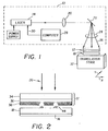
- a laser printing apparatus 10 for transferring material from a donor transfer element, which will hereinafter be referred to as a donor element 12 , onto a display substrate 18 in accordance with the present invention.
- the laser 14 of the printing apparatus 10 can be a diode laser or any other high power laser that produces a laser beam 26 . More than one laser or laser beam can be used simultaneously in this invention.
- a galvanometer 22 that includes a moveable mirror scans the beam through an f-theta lens 24 to form a line in direction X.
- scanning the laser beam can also be accomplished by other kinds of moveable mirrors, such as rotating polygons with mirror faces, or by other devices such as rotating diffraction gratings.
- donor element 12 and display substrate 18 are transported in a direction Y, which is orthogonal to the line, by a translation stage 32 allowing the full area to be scanned.
- the intensity of the beam at any point in the scan is controlled by the laser power control line 30 using instructions from the computer 28 .
- the intensity of the laser beam can be controlled by a separate modulator such as an acoustooptic modulator (not shown), as is well known by those skilled in the art of laser optics.
- the substrate can remain stationary and the laser apparatus is made to move or its beam redirected optically. The important feature is that there is relative movement between the laser beam and the display substrate in order to allow full area scanning.
- the donor element 12 is positioned in transfer relationship to display substrate 18 . Structure, materials, and fabrication of donor element 12 and display substrate 18 are discussed in more detail below.
- the donor element 12 and display substrate 18 may be held in this position by clamping, application of pressure, adhesives, or the like. It is preferred that transfer takes place under an inert atmosphere, such as nitrogen or argon, or vacuum. In a preferred embodiment, there is a gap maintained between the donor element and the portions of the display substrate to which material transfer is desired.
- the f-theta lens 24 focuses the laser beam onto radiation-absorbing layer 36 of donor element 12 while the galvanometer 22 scans the laser beam.
- the laser beam must have sufficient power to heat radiation-absorbing layer 36 to a temperature high enough to cause the material in organic layer 38 to transfer to display substrate 18 thereby forming transferred organic layer 44 . In one embodiment, this occurs by partial or full vaporization of the material in organic layer 38 with condensation onto the display substrate 18.
- the spot size caused by the f-theta lens 24 dictates the area of the organic layer that will be transferred.
- the arrangement is such that, when the laser beam has sufficient power for a given rate of scan, the spot size causes material from the illuminated portion of the light emissive layer to be selectively transferred from the donor element to designated areas corresponding to pixels on the display substrate.
- the laser beam is shown as two spaced arrows. For convenience of illustration, it will be understood that the laser beam 26 has actually been moved between two different positions where it is turned on for transferring portions of the organic layer 38 .
- the beam is continuously scanned by the galvanometer 22 across the donor element 12 while the laser power is modulated by instructions from the computer 28 .
- the modulation of laser power incident on the donor element 12 causes transfer of the organic material in organic layer 38 in selectable amounts in selected regions of the scan to the display substrate 18 . In a preferred embodiment, most or all of the material in organic layer 38 is transferred to substrate 18.
- the laser 14 can be an infrared solid-state laser, a neodynium YAG laser or any other laser providing a sufficient power to effect transfer of the organic layer.
- the power necessary will be dependent on the match between the absorption of the light-absorbing layer and the wavelength of the laser.
- the beam shape may be oval to allow small lines to be written while using low cost multimode laser, as taught in commonly assigned US-A-6,252,621 to David Kessler and others, the disclosure of which is hereby incorporated by reference.
- the process is repeated for separate pixel areas using a different donor element 12 with a different organic layer 38 that will produce light of a different color when the organic EL device is fully fabricated.
- donor element 12 used in the transfer process comprises a donor support 34 that is transmissive to the laser light, a radiation-absorbing layer 36 that converts the laser light into heat, and an organic layer 38 to be transferred.
- the organic layer 38 can also act as a radiation-absorbing layer and layer 36 can be eliminated.
- the support 34 can also serve as the radiation-absorbing layer, and separate layer 36 can be eliminated. Examples of donor support and radiation-absorbing materials that can be used in this invention can be found in US-A-4,772,582. The donor support must be capable of maintaining the structural integrity during the light-to-heat-induced transfer.
- the donor support must be capable of receiving on one surface a relatively thin coating of organic donor material, and of retaining this coating without degradation during anticipated storage periods of the coated support.
- Support materials meeting these requirements include, for example, glass, metal foils, plastic (polymeric) foils which exhibit a glass transition temperature value higher than a support temperature value anticipated during transfer, and fiber-reinforced plastic foils. Plastic foils are preferred. While selection of suitable support materials can rely on known engineering approaches, it will be appreciated that certain aspects of a selected support material merit further consideration when configured as a donor support useful in the practice of the invention. For example, the support can require a multistep cleaning and surface preparation process prior to precoating with transferable organic material.
- the material used in the radiation-absorbing layer 36 may be a dye such as the dyes specified in US-A-5,578,416 or a pigment such as carbon black.
- the radiation-absorbing layer may be a metal such as chromium, nickel or titanium, or a layered stack of materials that absorbs radiation by virtue of antireflection properties.
- the main criteria is that the light-absorbing layer absorbs at the wavelength of the laser emission with an optical density high enough to absorb most of the laser light, thereby producing sufficient heat to cause the organic layer to transfer. This transfer is well known to depend on the laser fluence, spot size, beam overlap and other factors. Generally, the optical density of the light-absorbing layer should be at least 0.1 ( ⁇ 20% of the light is absorbed).
- the heating element 16 can provide the same temperature or different temperatures for the donor element 12 and the display substrate 18. These temperatures should be in a range of greater than 30°C and less than 150°C, and more preferably, greater than 40 °C and less than 130 °C. The temperature should not exceed the vaporization temperature of the organic materials.
- the heating step should be applied prior to transfer of the organic layer 38 . It has been found advantageous to apply the heating step both before and during transfer of the organic layer 38 .
- the advantage conferred by the heating element 16 lies in the efficiency and stability of the final display element prepared by the methods described in this invention.
- the heating element 16 may be a block of metal with embedded electrical resistance heating elements, or means to circulate a heated fluid within the block, or any other convenient way of heating the block. In a useful embodiment, heating element 16 is placed in contact with the display substrate 18 . Heating element 16 may be part of the translation stage 32 , or attached to it. The heating element 16 may also consist of means for heating by infrared or visible radiation.
- heating element 16 is not limited to just this embodiment.
- the use of heating element 16 is advantageous when using any sort of radiation to heat the donor element in order to cause transfer of organic materials through vaporization whether patterned or not. This includes, for example, unpatterned or large area transfer of organic materials using a flash-lamp, an IR heater, resistive heating of a layer of the donor element by passage of an electrical current, or the like. Selective deposition is possible using any localized heating method including, but not limited to, using an optical mask between a flash-lamp and the donor. In all of these cases, the use of heater element 16 provides similar advantages as with laser-induced thermal transfer.
- display substrate 18 A general description of display substrate 18 , organic materials useful for organic EL displays, and other relevant information is provided below.
- the present invention can be employed in most OLED device configurations. These include very simple structures comprising a single anode and cathode to more complex devices, such as passive matrix displays comprised of orthogonal arrays of anodes and cathodes to form pixels, and active-matrix displays where each pixel is controlled independently, for example, with a thin film transistor (TFT).
- TFT thin film transistor
- FIG. 3 A typical, but not limiting, structure is shown in FIG. 3 and is comprised of a substrate 101 , independently addressable anodes 103, an optional hole-injecting layer 105, a hole-transporting layer 107, a light-emitting layer 109 further defined as 109R for red-emitting pixels, 109G for green-emitting pixels, and 109B for blue-emitting pixels, an electron-transporting layer 111, and a cathode layer 113 that may or may not be independently addressable.
- 109R red-emitting pixels
- 109G green-emitting pixels
- 109B blue-emitting pixels
- electron-transporting layer 111 an electron-transporting layer 111
- cathode layer 113 that may or may not be independently addressable.
- the substrate may alternatively be located adjacent to the cathode, or the substrate may actually constitute the anode or cathode.
- the electrode formed adjacent to the substrate is commonly referred to as the first electrode and the electrode formed after the organic EL materials have been deposited is commonly referred to as the second electrode.
- the first electrode is commonly formed in a patterned array that defines the RGB pixels. If low operating voltage is desired, the total combined thickness of the organic layers is preferably less than 500 nm.
- the layer transferred by this invention can be any one of the above.
- at least one of the layers transferred by this invention is a light-emitting layer and is formed over the patterned array of first electrodes in a spatially defined manner to create an array of pixels having a desired color, for example, red.
- These first electrodes are in electrical connection with the transferred light-emitting layer, either directly or through an intermediate layer such as the hole-transporting layer.
- other light-emitting layers are coated by the method of this invention to form arrays of other colored pixels, for example, green and blue.
- the light-emitting layer in each pixel is deposited by laser transfer and the other layers are blanket applied by conventional sublimation.
- the substrate 101 can either be light-transmissive or opaque, depending on the intended direction of light emission.
- the light-transmissive property is desirable for viewing the EL emission through the substrate.
- Transparent glass or plastic are commonly employed in such cases.
- the transmissive characteristic of the bottom support is immaterial, and therefore can be light-transmissive, light-absorbing or light reflective.
- Substrates for use in this case include, but are not limited to, glass, plastic, semiconductor materials, ceramics, and circuit board materials. Of course, it is necessary to provide in these device configurations a light-transparent top electrode.
- the conductive anode layer 103 is commonly formed over the substrate and, when EL emission is viewed through the anode, should be transparent or substantially transparent to the emission of interest.
- Common transparent anode materials used in this invention are indium-tin oxide (ITO) and tin oxide, but other metal oxides can work including, but not limited to, aluminum- or indium-doped zinc oxide (IZO), magnesium-indium oxide, and nickel-tungsten oxide.
- ITO indium-tin oxide
- IZO aluminum- or indium-doped zinc oxide
- IZO aluminum- or indium-doped zinc oxide
- nickel-tungsten oxide nickel-tungsten oxide.
- metal nitrides such as gallium nitride
- metal selenides such as zinc selenide
- metal sulfides such as zinc sulfide
- the transmissive characteristics of layer 103 are immaterial and any conductive material can be used, transparent, opaque or reflective.
- Example conductors for this application include, but are not limited to, gold, iridium, molybdenum, palladium, and platinum.
- Typical anode materials, transmissive or otherwise, have a work function of 4.1 eV or greater. Desired anode materials are commonly deposited by any suitable means such as evaporation, sputtering, chemical vapor deposition, or electrochemical means. Anodes can be patterned using well known photolithographic processes.
- a hole-injecting layer 105 be provided between anode 103 and hole-transporting layer 107 .
- the hole-injecting material can serve to improve the film formation property of subsequent organic layers and to facilitate injection of holes into the hole-transporting layer.
- Suitable materials for use in the hole-injecting layer include, but are not limited to, porphyrinic compounds as described in US-A-4,720,432, and plasma-deposited fluorocarbon polymers as described in US-A-6,208,075.
- Alternative hole-injecting materials reportedly useful in organic EL devices are described in EP 0 891 121 A1 and EP 1 029 909 A1.
- the hole-transporting layer 107 of the organic EL device contains at least one hole-transporting compound such as an aromatic tertiary amine, where the latter is understood to be a compound containing at least one trivalent nitrogen atom that is bonded only to carbon atoms, at least one of which is a member of an aromatic ring.
- the aromatic tertiary amine can be an arylamine, such as a monoarylamine, diarylamine, triarylamine, or a polymeric arylamine. Exemplary monomeric triarylamines are illustrated by Klupfel and others in US-A-3,180,730.
- Other suitable triarylamines substituted with one or more vinyl radicals and/or comprising at least one active hydrogen containing group are disclosed by Brantley and others US-A-3,567,450 and US-A-3,658,520.
- a more preferred class of aromatic tertiary amines are those which include at least two aromatic tertiary amine moieties as described in US-A-4,720,432 and US-A-5,061,569.
- Such compounds include those represented by structural formula (A). wherein:
- a useful class of triarylamines satisfying structural formula (A) and containing two triarylamine moieties is represented by structural formula (B): wherein:
- tetraaryldiamines Another class of aromatic tertiary amines are the tetraaryldiamines. Desirable tetraaryldiamines include two diarylamino groups, such as indicated by formula (C), linked through an arylene group. Useful tetraaryldiamines include those represented by formula (D). wherein:
- the various alkyl, alkylene, aryl, and arylene moieties of the foregoing structural formulae (A), (B), (C), (D), can each in turn be substituted.
- Typical substituents include alkyl groups, alkoxy groups, aryl groups, aryloxy groups, and halogen such as fluoride, chloride, and bromide.
- the various alkyl and alkylene moieties typically contain from about 1 to 6 carbon atoms.
- the cycloalkyl moieties can contain from 3 to about 10 carbon atoms, but typically contain five, six, or seven ring carbon atoms - for example, cyclopentyl, cyclohexyl, and cycloheptyl ring structures.
- the aryl and arylene moieties are usually phenyl and phenylene moieties.
- the hole-transporting layer can be formed of a single or a mixture of aromatic tertiary amine compounds.
- a triarylamine such as a triarylamine satisfying the formula (B)
- a tetraaryldiamine such as indicated by formula (D).
- a triarylamine is employed in combination with a tetraaryldiamine, the latter is positioned as a layer interposed between the triarylamine and the electron injecting and transporting layer.
- useful aromatic tertiary amines are the following:
- Another class of useful hole-transporting materials includes polycyclic aromatic compounds as described in EP 1 009 041.
- polymeric hole-transporting materials can be used such as poly(N-vinylcarbazole) (PVK), polythiophenes, polypyrrole, polyaniline, and copolymers such as poly(3,4-ethylenedioxythiophene)/poly(4-styrenesulfonate) also called PEDOT/PSS.
- the light-emitting layer (LEL) 109 of the organic EL element comprises a luminescent or fluorescent material where electroluminescence is produced as a result of electron-hole pair recombination in this region.
- the light-emitting layer can be comprised of a single material, but more commonly consists of a host material doped with a guest compound or compounds where light emission comes primarily from the dopant and can be of any color.
- the host materials in the light-emitting layer can be an electron-transporting material, as defined below, a hole-transporting material, as defined above, or another material or combination of materials that support hole-electron recombination.
- the dopant is usually chosen from highly fluorescent dyes, but phosphorescent compounds, for example, transition metal complexes as described in WO 98/55561, WO 00/18851, WO 00/57676, and WO 00/70655 are also useful. Dopants are typically coated as 0.01 to 10 % by weight into the host material. Different host/dopant combinations are used for different light-emitting pixels.
- Host and emitting molecules known to be of use include, but are not limited to, those disclosed in US-A-4,769,292; US-A-5,141,671; US-A-5,150,006; US-A-5,151,629; US-A-5,405,709; US-A-5,484,922; US-A-5,593,788; US-A-5,645,948; US-A-5,683,823; US-A-5,755,999; US-A-5,928,802; US-A-5,935,720; US-A-5,935,721, and US-A-6,020,078.
- Form E Metal complexes of 8-hydroxyquinoline and similar derivatives constitute one class of useful host compounds capable of supporting electroluminescence, and are particularly suitable for light emission of wavelengths longer than 500 nm, for example, green, yellow, orange, and red.
- the metal can be monovalent, divalent, trivalent, or tetravalent metal.
- the metal can, for example, be an alkali metal, such as lithium, sodium, or potassium; an alkaline earth metal, such as magnesium or calcium; an earth metal, such aluminum or gallium, or a transition metal such as zinc or zirconium.
- alkali metal such as lithium, sodium, or potassium
- alkaline earth metal such as magnesium or calcium
- earth metal such aluminum or gallium, or a transition metal such as zinc or zirconium.
- any monovalent, divalent, trivalent, or tetravalent metal known to be a useful chelating metal can be employed.
- Z completes a heterocyclic nucleus containing at least two fused aromatic rings, at least one of which is an azole or azine ring. Additional rings, including both aliphatic and aromatic rings, can be fused with the two required rings, if required. To avoid adding molecular bulk without improving on function, the number of ring atoms is usually maintained at 18 or less.
- Illustrative of useful chelated oxinoid compounds are the following:
- Form F 9,10-di-(2-naphthyl)anthracene
- Illustrative examples include 9,10-di-(2-naphthyl)anthracene and 2-t-butyl-9,10-di-(2-naphthyl)anthracene (TBADN).
- TAADN 2-t-butyl-9,10-di-(2-naphthyl)anthracene
- Other anthracene derivatives can be useful as a host in the LEL, including derivatives of 9,10-bis[4-(2,2-diphenylethenyl)phenyl]anthracene.
- Benzazole derivatives constitute another class of useful hosts capable of supporting electroluminescence, and are particularly suitable for light emission of wavelengths longer than 400 nm, for example, blue, green, yellow, orange or red.
- L is a linkage unit consisting of alkyl, aryl, substituted alkyl, or substituted aryl, which conjugately or unconjugately connects the multiple benzazoles together.
- An example of a useful benzazole is 2, 2', 2"-(1,3,5-phenylene)tris [1-phenyl-1H-benzimidazole].
- Desirable fluorescent dopants include derivatives of anthracene, tetracene, xanthene, perylene, rubrene, coumarin, rhodamine, quinacridone, dicyanomethylenepyran compounds, thiopyran compounds, polymethine compounds, pyrilium and thiapyrilium compounds, and carbostyryl compounds.
- Illustrative examples of useful dopants include, but are not limited to, the following:
- Preferred thin film-forming materials for use in forming the electron-transporting layer 111 of the organic EL devices of this invention are metal chelated oxinoid compounds, including chelates of oxine itself (also commonly referred to as 8-quinolinol or 8-hydroxyquinoline). Such compounds help to inject and transport electrons and exhibit both high levels of performance and are readily fabricated in the form of thin films.
- exemplary of contemplated oxinoid compounds are those satisfying structural formula (E), previously described.
- electron-transporting materials include various butadiene derivatives as disclosed in US-A-4,356,429 and various heterocyclic optical brighteners as described in US-A-4,539,507.
- Benzazoles satisfying structural formula (G) are also useful electron transporting materials.
- layers 109 and 111 can optionally be collapsed into a single layer that serves the function of supporting both light emission and electron transportation.
- layers 109 and 107 can optionally be collapsed into a single layer that serves the function of supporting both light emission and hole transportation.
- the cathode layer 113 used in this invention can be comprised of nearly any conductive material. Desirable materials have good film-forming properties to ensure good contact with the underlying organic layer, promote electron injection at low voltage, and have good stability. Useful cathode materials often contain a low work function metal ( ⁇ 4.0 eV) or metal alloy.
- a low work function metal ⁇ 4.0 eV
- One preferred cathode material is comprised of a Mg:Ag alloy wherein the percentage of silver is in the range of 1 to 20 %, as described in US-A-4,885,221.
- Another suitable class of cathode materials includes bilayers comprised of a thin layer of a low work function metal or metal salt capped with a thicker layer of conductive metal.
- cathode is comprised of a thin layer of LiF followed by a thicker layer of A1 as described in US-A-5,677,572.
- Other useful cathode materials include, but are not limited to, those disclosed in US-A-5,059,861; US-A-5,059,862; and US-A-6,140,763.
- cathode When light emission is viewed through the cathode, the cathode must be transparent or nearly transparent. For such applications, metals must be thin or one must use transparent conductive oxides, or a combination of these materials.
- Optically transparent cathodes have been described in more detail in US-A-5,776,623. Cathode materials can be deposited by evaporation, sputtering, or chemical vapor deposition. When needed, patterning can be achieved through many well known methods including, but not limited to, through-mask deposition, integral shadow masking as described in US-A-5,276,380 and EP 0 732 868, laser ablation, and selective chemical vapor deposition.
- Non-patternwise deposition of the organic materials mentioned above, for example, onto the display substrate 18 or to form organic layer 38 over the donor support, is suitably accomplished through sublimation.
- organic materials may also deposited from a solvent with an optional binder to improve film formation. If the material is a polymer, solvent deposition is usually preferred.
- the material to be deposited by sublimation can be vaporized from a sublimator "boat" often comprised of a tantalum material, for example, as described in US-A-6,237,529. Note that layers not requiring patterning may first be deposited onto a support to form donor element 12 and then sublimed in closer proximity to the substrate via unpatterned flash-lamp deposition. Layers requiring a mixture of materials can utilize separate sublimator boats or the materials can be premixed and coated from a single boat or donor sheet.
- OLED devices are sensitive to moisture and/or oxygen so they are commonly sealed in an inert atmosphere such as nitrogen or argon, along with a desiccant such as alumina, bauxite, calcium sulfate, clays, silica gel, zeolites, alkaline metal oxides, alkaline earth metal oxides, sulfates, or metal halides and perchlorates.
- a desiccant such as alumina, bauxite, calcium sulfate, clays, silica gel, zeolites, alkaline metal oxides, alkaline earth metal oxides, sulfates, or metal halides and perchlorates.
- a donor element was formed by the vacuum deposition of a radiation-absorbing layer of 60 nm of chromium on a 125 ⁇ m polyimide donor support. Onto this substrate was vacuum deposited a 2.5 nanometer thick layer of CO-1 (ALQ) and 0.2 nm of L39 (DCJTB), 11 nm of TBADN and 0.6 nm of NPB.
- a clean glass substrate was vacuum deposited through a mask with indium tin oxide (ITO) to pattern 40 to 80 nm transparent first electrodes (anodes).
- ITO indium tin oxide
- a plasma oxygen etch followed by plasma deposition of ⁇ 0.1 nm of CF x was used as a hole-injecting layer over the ITO surface.
- a 75 nm NPB hole-transporting layer was then vacuum deposited.
- a donor element as previously described was placed on top of the NPB layer and held in proximal contact using vacuum. A small gap was maintained by the by the texture of the donor substrate that had surface roughness features approximately 2 micrometers high.
- the stage was heated to the temperature indicated in Table 1.
- Laser transfer of the light emissive material was effected from the donor element to the display substrate by irradiation of the donor element through the substrate with an infrared laser beam.
- the beam size was approximately 16 micrometers by 80 micrometers to the 1/e 2 point scanning along the wide beam direction.
- the dwell time was 27 microseconds with a power density as listed. Transfer was effected in regions, which were desired to be red colored.
- Heating to 60°C generated a red hue (peak emission wavelength) that is preferred to that generated without the heating. Heating to 60 °C also yielded slightly higher initial luminance. Of particular note, the stability was greatly enhanced by heating during the transfer as evidenced by the higher luminance after 100 hours.
- a donor element was formed by the vacuum deposition of a radiation-absorpting layer of 60 nanometers of chromium on a 125 ⁇ m polyimide donor support. Onto this was vacuum deposited a 18.7 nanometer thick layer of ALQ, 18.7 nanometers of TBADN and 0.2 nanometers of green dopant L7. This donor was used to make a light emitting diode as described in the previous example. Transfer was effected where green emission was desired. Device testing consisted of putting a constant current through the diodes and monitoring the light output. These data are shown in Table 2.
- Heating to 60°C generated a green hue (peak emission wavelength) that is preferred to that generated at 37 °C.
- the stability was greatly enhanced.
- the luminance increased over time for the device heated to 60 °C as evidenced by the higher luminance after 100 hours.
- said device also comprises a hole-transporting layer and an electron-transporting layer.
- the donor element also comprises a radiation-absorbing layer between the donor substrate and the organic material to be transferred.
- the method wherein the temperature range is greater than 40 °C and less than 130 °C.
Abstract
Description
- The present invention relates to a method of making organic electroluminescent devices and, more particularly, to using radiation-induced thermal transfer of organic materials to produce display elements.
- In color or full-color organic electroluminescent (EL) displays having an array of colored pixels such as red, green, and blue color pixels (commonly referred to as RGB pixels), precision patterning of the color producing organic EL media is required to produce the RGB pixels. The basic organic EL device has in common an anode, a cathode, and an organic EL medium sandwiched between the anode and the cathode. The organic EL medium may consist of one or more layers of organic thin films, where one of the layers or regions within a layer is primarily responsible for light generation or electroluminescence. This particular layer is generally referred to as the light-emitting layer of the organic EL medium. Other organic layers that may be present in the organic EL medium commonly facilitate electronic transportation, such as a hole-transporting layer (for hole conduction) or an electron-transporting layer (for electron conduction). In forming the RGB pixels in a full-color organic EL display panel, it is necessary to devise a method to precisely pattern the light-emitting layer of the organic EL medium or the entire organic EL medium. There is also a desire to increase efficiency and stability to as high as possible.
- Typically, electroluminescent pixels are formed on the display by shadow masking techniques, such as shown in US-A-5,742,129. Although this has been effective, it has several drawbacks. It has been difficult to achieve high resolution of pixel sizes using shadow masking. Moreover, there are problems of alignment between the substrate and the shadow mask, and care must be taken that pixels are formed in the appropriate locations. When it is desirable to increase the substrate size, it is difficult to manipulate the shadow mask to form appropriately positioned pixels. A further disadvantage of the shadow mask method is that the mask holes can become plugged with time. Plugged holes on the mask lead to the undesirable result of nonfunctioning pixels on the EL display.
- There are further problems with the shadow mask method, which become especially apparent when making EL devices with dimensions of more than a few inches on a side. It is extremely difficult to manufacture larger shadow masks with the required precision (hole position of ±5 micrometers) for accurately forming EL devices.
- A method for patterning high resolution organic EL displays has been disclosed in US-A-5,851,709 by Grande and others. This method is comprised of the following sequences of steps: 1) providing a donor substrate having opposing first and second surfaces; 2) forming a light-transmissive, heat-insulating layer over the first surface of the donor substrate; 3) forming a light-absorbing layer over the heat-insulating layer; 4) providing the donor substrate with an array of openings extending from the second surface to the heat-insulating layer; 5) providing a transferable, color forming, organic donor layer formed on the light-absorbing layer; 6) precision aligning the donor substrate with the display substrate in an oriented relationship between the openings in the substrate and the corresponding color pixels on the device; and 7) employing a source of radiation for producing sufficient heat at the light-absorbing layer over the openings to cause the transfer of the organic layer on the donor substrate to the display substrate. A problem with the Grande and others approach is that patterning of an array of openings on the donor substrate is required. This creates many of the same problems as the shadow mask method, including the requirement for precision mechanical alignment between the donor substrate and the display substrate. A further problem is that the donor pattern is fixed and cannot be changed readily.
- Using an unpatterned donor sheet and a precision light source, such as a laser, can remove some of the difficulties seen with a patterned donor. Such a method is disclosed by Littman in US-A-5,688,551, and in a series of patents by Wolk and others (US-A-6,114,088; US-A-6,140,009; US-A-6,214,520; and US-A-6,221,553). However, it has been found that the properties of the organic display materials transferred by a laser can be inferior to those deposited by conventional vapor deposition methods. Such properties include uniformity, efficiency, and stability. Thus, in order to take full advantage of the patterning advantages offered by radiation-induced thermal transfer, a need remains to improve the properties of the transferred material.
- It is an object of the present invention to provide a method for patterning the organic EL medium without the limitations imposed by the conventional photolithographic or shadow mask methods.
- It is another object of the present invention to provide an improved method for patterning high resolution, full color, organic EL displays.
- It is another object of the invention to provide a method for patterning high resolution color EL displays without the limitation of mechanical precision alignment and allowing for dynamic alignment and simple pattern changes.
- It is also an object of this invention to increase the efficiency and lifetime of the organic EL displays.
- These objects are achieved by a method for making an organic electroluminescent display device having an array of pixels disposed on a display substrate, comprising the steps of:
- a) providing an array of first electrodes on a display substrate;
- b) providing a donor element comprising a donor support, a radiation-absorbing layer over the donor support, and at least one organic layer over the radiation-absorbing layer, wherein said organic layer comprises the material or materials to be transferred to the display substrate;
- c) positioning the donor element in transfer relationship to the display substrate patterned with an array of first electrodes;
- d) heating the display substrate or donor element or both within a specified temperature range prior to transfer of the organic layer;
- e) focusing and scanning a laser beam of sufficient power and desired spot size on the radiation-absorbing layer of the donor element to effect the transfer of selected portions of the organic layer from the donor element to designated areas corresponding to pixels on the display substrate in electrical connection with the first electrodes; and
- f) providing a second electrode over the transferred organic portions on the display substrate.
-
- The present invention provides an advantage in that the heating step prior to radiation-induced thermal transfer yields an organic EL display with higher efficiency and higher stability. This invention is particularly suitable for making full color, organic EL displays with high quality, good efficiency, and stability. By printing with a scanning laser beam, fine precision patterning of colored pixels can be achieved, enabling the production of high resolution displays.
- FIG. 1 shows a schematic drawing of an apparatus that is useful for transferring portions of an organic layer onto a display substrate from a donor element:
- FIG. 2 is a cross sectional view which depicts, in more detail, the display substrate and the donor element with a heating element; and
- FIG. 3 shows, in cross section, a schematic of a full color organic electroluminescent display device.
-
- Turning now to FIG. 1, there is shown a
laser printing apparatus 10 for transferring material from a donor transfer element, which will hereinafter be referred to as adonor element 12, onto adisplay substrate 18 in accordance with the present invention. Thelaser 14 of theprinting apparatus 10 can be a diode laser or any other high power laser that produces alaser beam 26. More than one laser or laser beam can be used simultaneously in this invention. In order to scan the laser beam to provide relative movement betweenlaser beam 26 anddonor element 12, agalvanometer 22 that includes a moveable mirror scans the beam through an f-theta lens 24 to form a line in direction X. Those skilled in the art will understand that scanning the laser beam can also be accomplished by other kinds of moveable mirrors, such as rotating polygons with mirror faces, or by other devices such as rotating diffraction gratings. - In the embodiment shown in FIG. 1,
donor element 12 anddisplay substrate 18 are transported in a direction Y, which is orthogonal to the line, by atranslation stage 32 allowing the full area to be scanned. The intensity of the beam at any point in the scan is controlled by the laserpower control line 30 using instructions from thecomputer 28. Alternatively, the intensity of the laser beam can be controlled by a separate modulator such as an acoustooptic modulator (not shown), as is well known by those skilled in the art of laser optics. In an alternative embodiment, the substrate can remain stationary and the laser apparatus is made to move or its beam redirected optically. The important feature is that there is relative movement between the laser beam and the display substrate in order to allow full area scanning. - As shown in FIG. 2, the
donor element 12 is positioned in transfer relationship to displaysubstrate 18. Structure, materials, and fabrication ofdonor element 12 anddisplay substrate 18 are discussed in more detail below. Thedonor element 12 anddisplay substrate 18 may be held in this position by clamping, application of pressure, adhesives, or the like. It is preferred that transfer takes place under an inert atmosphere, such as nitrogen or argon, or vacuum. In a preferred embodiment, there is a gap maintained between the donor element and the portions of the display substrate to which material transfer is desired. - The f-
theta lens 24 focuses the laser beam onto radiation-absorbing layer 36 ofdonor element 12 while thegalvanometer 22 scans the laser beam. The laser beam must have sufficient power to heat radiation-absorbing layer 36 to a temperature high enough to cause the material inorganic layer 38 to transfer todisplay substrate 18 thereby forming transferredorganic layer 44. In one embodiment, this occurs by partial or full vaporization of the material inorganic layer 38 with condensation onto thedisplay substrate 18. The spot size caused by the f-theta lens 24 dictates the area of the organic layer that will be transferred. The arrangement is such that, when the laser beam has sufficient power for a given rate of scan, the spot size causes material from the illuminated portion of the light emissive layer to be selectively transferred from the donor element to designated areas corresponding to pixels on the display substrate. In FIG. 2, the laser beam is shown as two spaced arrows. For convenience of illustration, it will be understood that thelaser beam 26 has actually been moved between two different positions where it is turned on for transferring portions of theorganic layer 38. - In a preferred embodiment, the beam is continuously scanned by the
galvanometer 22 across thedonor element 12 while the laser power is modulated by instructions from thecomputer 28. The modulation of laser power incident on thedonor element 12 causes transfer of the organic material inorganic layer 38 in selectable amounts in selected regions of the scan to thedisplay substrate 18. In a preferred embodiment, most or all of the material inorganic layer 38 is transferred tosubstrate 18. - The
laser 14 can be an infrared solid-state laser, a neodynium YAG laser or any other laser providing a sufficient power to effect transfer of the organic layer. The power necessary will be dependent on the match between the absorption of the light-absorbing layer and the wavelength of the laser. The beam shape may be oval to allow small lines to be written while using low cost multimode laser, as taught in commonly assigned US-A-6,252,621 to David Kessler and others, the disclosure of which is hereby incorporated by reference. - To create a multicolor or full color display, the process is repeated for separate pixel areas using a
different donor element 12 with a differentorganic layer 38 that will produce light of a different color when the organic EL device is fully fabricated. - In the preferred embodiment,
donor element 12 used in the transfer process comprises adonor support 34 that is transmissive to the laser light, a radiation-absorbing layer 36 that converts the laser light into heat, and anorganic layer 38 to be transferred. In separate embodiments, theorganic layer 38 can also act as a radiation-absorbing layer and layer 36 can be eliminated. Alternatively, thesupport 34 can also serve as the radiation-absorbing layer, and separate layer 36 can be eliminated. Examples of donor support and radiation-absorbing materials that can be used in this invention can be found in US-A-4,772,582. The donor support must be capable of maintaining the structural integrity during the light-to-heat-induced transfer. Additionally, the donor support must be capable of receiving on one surface a relatively thin coating of organic donor material, and of retaining this coating without degradation during anticipated storage periods of the coated support. Support materials meeting these requirements include, for example, glass, metal foils, plastic (polymeric) foils which exhibit a glass transition temperature value higher than a support temperature value anticipated during transfer, and fiber-reinforced plastic foils. Plastic foils are preferred. While selection of suitable support materials can rely on known engineering approaches, it will be appreciated that certain aspects of a selected support material merit further consideration when configured as a donor support useful in the practice of the invention. For example, the support can require a multistep cleaning and surface preparation process prior to precoating with transferable organic material. - The material used in the radiation-absorbing layer 36 may be a dye such as the dyes specified in US-A-5,578,416 or a pigment such as carbon black. The radiation-absorbing layer may be a metal such as chromium, nickel or titanium, or a layered stack of materials that absorbs radiation by virtue of antireflection properties. The main criteria is that the light-absorbing layer absorbs at the wavelength of the laser emission with an optical density high enough to absorb most of the laser light, thereby producing sufficient heat to cause the organic layer to transfer. This transfer is well known to depend on the laser fluence, spot size, beam overlap and other factors. Generally, the optical density of the light-absorbing layer should be at least 0.1 (∼20% of the light is absorbed).
- An important feature of the present invention is the incorporation of a
heating element 16 for thedonor element 12 and thedisplay substrate 18. Theheating element 16 can provide the same temperature or different temperatures for thedonor element 12 and thedisplay substrate 18. These temperatures should be in a range of greater than 30°C and less than 150°C, and more preferably, greater than 40 °C and less than 130 °C. The temperature should not exceed the vaporization temperature of the organic materials. The heating step should be applied prior to transfer of theorganic layer 38. It has been found advantageous to apply the heating step both before and during transfer of theorganic layer 38. The advantage conferred by theheating element 16 lies in the efficiency and stability of the final display element prepared by the methods described in this invention. While the comprehensive mechanism of this improvement is not presently completely understood at this time, it appears that a higher temperature during the time of laser transfer of theorganic layer 38 provides more uniform distribution and better activation of the materials of the transferredorganic layer 44. Whatever the details of the mechanism of improvement are, it is observed that displays made by the method of this invention are of higher efficiency and better stability than those made without heating. - The
heating element 16 may be a block of metal with embedded electrical resistance heating elements, or means to circulate a heated fluid within the block, or any other convenient way of heating the block. In a useful embodiment,heating element 16 is placed in contact with thedisplay substrate 18.Heating element 16 may be part of thetranslation stage 32, or attached to it. Theheating element 16 may also consist of means for heating by infrared or visible radiation. - While the foregoing description employs a laser for selective deposition of organic materials, it will be appreciated that use of the
heating element 16 is not limited to just this embodiment. The use ofheating element 16 is advantageous when using any sort of radiation to heat the donor element in order to cause transfer of organic materials through vaporization whether patterned or not. This includes, for example, unpatterned or large area transfer of organic materials using a flash-lamp, an IR heater, resistive heating of a layer of the donor element by passage of an electrical current, or the like. Selective deposition is possible using any localized heating method including, but not limited to, using an optical mask between a flash-lamp and the donor. In all of these cases, the use ofheater element 16 provides similar advantages as with laser-induced thermal transfer. - A general description of
display substrate 18, organic materials useful for organic EL displays, and other relevant information is provided below. - The present invention can be employed in most OLED device configurations. These include very simple structures comprising a single anode and cathode to more complex devices, such as passive matrix displays comprised of orthogonal arrays of anodes and cathodes to form pixels, and active-matrix displays where each pixel is controlled independently, for example, with a thin film transistor (TFT). This invention is most advantageous when applied to full color display device fabrication.
- There are numerous configurations of the organic layers known in the art wherein the present invention can be successfully practiced. A typical, but not limiting, structure is shown in FIG. 3 and is comprised of a
substrate 101, independentlyaddressable anodes 103, an optional hole-injecting layer 105, a hole-transportinglayer 107, a light-emitting layer 109 further defined as 109R for red-emitting pixels, 109G for green-emitting pixels, and 109B for blue-emitting pixels, an electron-transportinglayer 111, and acathode layer 113 that may or may not be independently addressable. These layers are described in detail below. Note that the substrate may alternatively be located adjacent to the cathode, or the substrate may actually constitute the anode or cathode. The electrode formed adjacent to the substrate is commonly referred to as the first electrode and the electrode formed after the organic EL materials have been deposited is commonly referred to as the second electrode. The first electrode is commonly formed in a patterned array that defines the RGB pixels. If low operating voltage is desired, the total combined thickness of the organic layers is preferably less than 500 nm. - The layer transferred by this invention, that is, by radiation-induced thermal transfer, can be any one of the above. Most preferably, at least one of the layers transferred by this invention is a light-emitting layer and is formed over the patterned array of first electrodes in a spatially defined manner to create an array of pixels having a desired color, for example, red. These first electrodes are in electrical connection with the transferred light-emitting layer, either directly or through an intermediate layer such as the hole-transporting layer. Similarly, other light-emitting layers are coated by the method of this invention to form arrays of other colored pixels, for example, green and blue. By coating multiple layers onto
donor element 12, multiple layers or materials can be transferred to displaysubstrate 18. Depending on conditions, this transfer can occur with little, partial, or complete mixing of layers. Other layers that do not require precision patterning may be coated by any number of methods described below. In one useful embodiment, the light-emitting layer in each pixel is deposited by laser transfer and the other layers are blanket applied by conventional sublimation. - The
substrate 101 can either be light-transmissive or opaque, depending on the intended direction of light emission. The light-transmissive property is desirable for viewing the EL emission through the substrate. Transparent glass or plastic are commonly employed in such cases. For applications where the EL emission is viewed through the top electrode, the transmissive characteristic of the bottom support is immaterial, and therefore can be light-transmissive, light-absorbing or light reflective. Substrates for use in this case include, but are not limited to, glass, plastic, semiconductor materials, ceramics, and circuit board materials. Of course, it is necessary to provide in these device configurations a light-transparent top electrode. - The
conductive anode layer 103 is commonly formed over the substrate and, when EL emission is viewed through the anode, should be transparent or substantially transparent to the emission of interest. Common transparent anode materials used in this invention are indium-tin oxide (ITO) and tin oxide, but other metal oxides can work including, but not limited to, aluminum- or indium-doped zinc oxide (IZO), magnesium-indium oxide, and nickel-tungsten oxide. In addition to these oxides, metal nitrides, such as gallium nitride, and metal selenides, such as zinc selenide, and metal sulfides, such as zinc sulfide, can be used inlayer 103. For applications where EL emission is viewed through the top electrode, the transmissive characteristics oflayer 103 are immaterial and any conductive material can be used, transparent, opaque or reflective. Example conductors for this application include, but are not limited to, gold, iridium, molybdenum, palladium, and platinum. Typical anode materials, transmissive or otherwise, have a work function of 4.1 eV or greater. Desired anode materials are commonly deposited by any suitable means such as evaporation, sputtering, chemical vapor deposition, or electrochemical means. Anodes can be patterned using well known photolithographic processes. - While not always necessary, it is often useful that a hole-injecting layer 105 be provided between
anode 103 and hole-transportinglayer 107. The hole-injecting material can serve to improve the film formation property of subsequent organic layers and to facilitate injection of holes into the hole-transporting layer. Suitable materials for use in the hole-injecting layer include, but are not limited to, porphyrinic compounds as described in US-A-4,720,432, and plasma-deposited fluorocarbon polymers as described in US-A-6,208,075. Alternative hole-injecting materials reportedly useful in organic EL devices are described in EP 0 891 121 A1 andEP 1 029 909 A1. - The hole-transporting
layer 107 of the organic EL device contains at least one hole-transporting compound such as an aromatic tertiary amine, where the latter is understood to be a compound containing at least one trivalent nitrogen atom that is bonded only to carbon atoms, at least one of which is a member of an aromatic ring. In one form the aromatic tertiary amine can be an arylamine, such as a monoarylamine, diarylamine, triarylamine, or a polymeric arylamine. Exemplary monomeric triarylamines are illustrated by Klupfel and others in US-A-3,180,730. Other suitable triarylamines substituted with one or more vinyl radicals and/or comprising at least one active hydrogen containing group are disclosed by Brantley and others US-A-3,567,450 and US-A-3,658,520. - A more preferred class of aromatic tertiary amines are those which include at least two aromatic tertiary amine moieties as described in US-A-4,720,432 and US-A-5,061,569. Such compounds include those represented by structural formula (A).wherein:

- Q1 and Q2 are independently selected aromatic tertiary amine moieties; and
- G is a linking group such as an arylene, cycloalkylene, or alkylene group of a carbon to carbon bond. In one embodiment, at least one of Q1 or Q2 contains a polycyclic fused ring structure, for example, a naphthalene. When G is an aryl group, it is conveniently a phenylene, biphenylene, or naphthalene moiety.
-
- A useful class of triarylamines satisfying structural formula (A) and containing two triarylamine moieties is represented by structural formula (B):wherein:

- R1 and R2 each independently represents a hydrogen atom, an aryl group, or an alkyl group or R1 and R2 together represent the atoms completing a cycloalkyl group; and
- R3 and R4 each independently represents an aryl group, which is in turn
substituted with a diaryl substituted amino group, as indicated by structural
formula (C):
 wherein:
- R5 and R6 are independently selected aryl groups. In one embodiment, at least one of R5 or R6 contains a polycyclic fused ring structure, for example, a naphthalene.
-
- Another class of aromatic tertiary amines are the tetraaryldiamines. Desirable tetraaryldiamines include two diarylamino groups, such as indicated by formula (C), linked through an arylene group. Useful tetraaryldiamines include those represented by formula (D).wherein:

- each Are is an independently selected arylene group, such as a phenylene or anthracene moiety;
- n is an integer of from 1 to 4; and
- Ar, R7, R8, and R9 are independently selected aryl groups. In a typical embodiment, at least one of Ar, R7, R8, and R9 is a polycyclic fused ring structure, for example, a naphthalene
-
- The various alkyl, alkylene, aryl, and arylene moieties of the foregoing structural formulae (A), (B), (C), (D), can each in turn be substituted. Typical substituents include alkyl groups, alkoxy groups, aryl groups, aryloxy groups, and halogen such as fluoride, chloride, and bromide. The various alkyl and alkylene moieties typically contain from about 1 to 6 carbon atoms. The cycloalkyl moieties can contain from 3 to about 10 carbon atoms, but typically contain five, six, or seven ring carbon atoms - for example, cyclopentyl, cyclohexyl, and cycloheptyl ring structures. The aryl and arylene moieties are usually phenyl and phenylene moieties.
- The hole-transporting layer can be formed of a single or a mixture of aromatic tertiary amine compounds. Specifically, one may employ a triarylamine, such as a triarylamine satisfying the formula (B), in combination with a tetraaryldiamine, such as indicated by formula (D). When a triarylamine is employed in combination with a tetraaryldiamine, the latter is positioned as a layer interposed between the triarylamine and the electron injecting and transporting layer. Illustrative of useful aromatic tertiary amines are the following:
- 1,1-Bis(4-di- p -tolylaminophenyl)cyclohexane
- 1,1-Bis(4-di- p -tolylaminophenyl)-4-phenylcyclohexane
- 4,4'-Bis(diphenylamino)quadriphenyl
- Bis(4-dimethylamino-2-methylphenyl)-phenylmethane
- N,N,N-Tri( p -tolyl)amine
- 4-(di-p-tolylamino)-4'-[4(di- p -tolylamino)-styryl]stilbene
- N,N,N',N'-Tetra- p -tolyl-4-4'-diaminobiphenyl
- N,N,N',N'-Tetraphenyl-4,4'-diaminobiphenyl
- N,N,N',N'-tetra-1-naphthyl-4,4'-diaminobiphenyl
- N,N,N',N'-tetra-2-naphthyl-4,4'-diaminobiphenyl
- N-Phenylcarbazole
- 4,4'-Bis[N-(1-naphthyl)-N-phenylamino]biphenyl
- 4,4'-Bis[N-(1-naphthyl)-N-(2-naphthyl)amino]biphenyl
- 4,4"-Bis[N-(1-naphthyl)-N-phenylamino]p-terphenyl
- 4,4'-Bis[N-(2-naphthyl)-N-phenylamino]biphenyl (NPB)
- 4,4'-Bis[N-(3-acenaphthenyl)-N-phenylamino]biphenyl
- 1,5-Bis[N-(1-naphthyl)-N-phenylamino]naphthalene
- 4,4'-Bis[N-(9-anthryl)-N-phenylamino]biphenyl
- 4,4"-Bis[N-(1-anthryl)-N-phenylamino]- p -terphenyl
- 4,4'-Bis[N-(2-phenanthryl)-N-phenylamino]biphenyl
- 4,4'-Bis[N-(8-fluoranthenyl)-N-phenylamino]biphenyl
- 4,4'-Bis[N-(2-pyrenyl)-N-phenylamino]biphenyl
- 4,4'-Bis[N-(2-naphthacenyl)-N-phenylamino]biphenyl
- 4,4'-Bis[N-(2-perylenyl)-N-phenylamino]biphenyl
- 4,4'-Bis[N-( 1-coronenyl)-N-phenylamino]biphenyl
- 2,6-Bis(di- p -tolylamino)naphthalene
- 2,6-Bis[di-(1-naphthyl)amino]naphthalene
- 2,6-Bis[N-(1-naphthyl)-N-(2-naphthyl)amino]naphthalene
- N,N,N',N'-Tetra(2-naphthyl)-4,4"-diamino- p -terphenyl
- 4,4'-Bis{N-phenyl-N-[4-(1-naphthyl)-phenyl]amino}biphenyl
- 4,4'-Bis[N-phenyl-N-(2-pyrenyl)amino]biphenyl
- 2,6-Bis[N,N-di(2-naphthyl)amine]fluorene
- 1,5-Bis[N-(1-naphthyl)-N-phenylamino]naphthalene
-
- Another class of useful hole-transporting materials includes polycyclic aromatic compounds as described in
EP 1 009 041. In addition, polymeric hole-transporting materials can be used such as poly(N-vinylcarbazole) (PVK), polythiophenes, polypyrrole, polyaniline, and copolymers such as poly(3,4-ethylenedioxythiophene)/poly(4-styrenesulfonate) also called PEDOT/PSS. - As more fully described in US-A-4,769,292 and US-A-5,935,721, the light-emitting layer (LEL) 109 of the organic EL element comprises a luminescent or fluorescent material where electroluminescence is produced as a result of electron-hole pair recombination in this region. The light-emitting layer can be comprised of a single material, but more commonly consists of a host material doped with a guest compound or compounds where light emission comes primarily from the dopant and can be of any color. The host materials in the light-emitting layer can be an electron-transporting material, as defined below, a hole-transporting material, as defined above, or another material or combination of materials that support hole-electron recombination. The dopant is usually chosen from highly fluorescent dyes, but phosphorescent compounds, for example, transition metal complexes as described in WO 98/55561, WO 00/18851, WO 00/57676, and WO 00/70655 are also useful. Dopants are typically coated as 0.01 to 10 % by weight into the host material. Different host/dopant combinations are used for different light-emitting pixels.
- An important relationship for choosing a dye as a dopant is a comparison of the bandgap potential which is defined as the energy difference between the highest occupied molecular orbital and the lowest unoccupied molecular orbital of the molecule. For efficient energy transfer from the host to the dopant molecule, a necessary condition is that the band gap of the dopant is smaller than that of the host material.
- Host and emitting molecules known to be of use include, but are not limited to, those disclosed in US-A-4,769,292; US-A-5,141,671; US-A-5,150,006; US-A-5,151,629; US-A-5,405,709; US-A-5,484,922; US-A-5,593,788; US-A-5,645,948; US-A-5,683,823; US-A-5,755,999; US-A-5,928,802; US-A-5,935,720; US-A-5,935,721, and US-A-6,020,078.
- Metal complexes of 8-hydroxyquinoline and similar derivatives (Formula E) constitute one class of useful host compounds capable of supporting electroluminescence, and are particularly suitable for light emission of wavelengths longer than 500 nm, for example, green, yellow, orange, and red.wherein:

- M represents a metal;
- n is an integer of from 1 to 4; and
- Z independently in each occurrence represents the atoms completing a nucleus having at least two fused aromatic rings.
-
- From the foregoing it is apparent that the metal can be monovalent, divalent, trivalent, or tetravalent metal. The metal can, for example, be an alkali metal, such as lithium, sodium, or potassium; an alkaline earth metal, such as magnesium or calcium; an earth metal, such aluminum or gallium, or a transition metal such as zinc or zirconium. Generally any monovalent, divalent, trivalent, or tetravalent metal known to be a useful chelating metal can be employed.
- Z completes a heterocyclic nucleus containing at least two fused aromatic rings, at least one of which is an azole or azine ring. Additional rings, including both aliphatic and aromatic rings, can be fused with the two required rings, if required. To avoid adding molecular bulk without improving on function, the number of ring atoms is usually maintained at 18 or less.
- Illustrative of useful chelated oxinoid compounds are the following:
- CO-1: Aluminum trisoxine [alias, tris(8-quinolinolato)aluminum(III), alias ALQ]
- CO-2: Magnesium bisoxine [alias, bis(8-quinolinolato)magnesium(II)]
- CO-3: Bis[benzo{f}-8-quinolinolato]zinc (II)
- CO-4: Bis(2-methyl-8-quinolinolato)aluminum(III)-µ-oxo-bis(2-methyl-8-quinolinolato) aluminum(III)
- CO-5: Indium trisoxine [alias, tris(8-quinolinolato)indium]
- CO-6: Aluminum tris(5-methyloxine) [alias, tris(5-methyl-8-quinolinolato) aluminum(III)]
- CO-7: Lithium oxine [alias, (8-quinolinolato)lithium(I)]
- CO-8: Gallium oxine [alias, tris(8-quinolinolato)gallium(III)]
- CO-9: Zirconium oxine [alias, tetra(8-quinolinolato)zirconium(IV)]
-
- Derivatives of 9,10-di-(2-naphthyl)anthracene (Formula F) constitute one class of useful hosts capable of supporting electroluminescence, and are particularly suitable for light emission of wavelengths longer than 400 nm, for example, blue, green, yellow, orange or red.wherein:

- R1, R2, R3, R4, R5, and R6 represent one or more substituents on each ring
where each substituent is individually selected from the following groups:
- Group 1: hydrogen, or alkyl of from 1 to 24 carbon atoms;
- Group 2: aryl or substituted aryl of from 5 to 20 carbon atoms;
- Group 3: carbon atoms from 4 to 24 necessary to complete a fused aromatic ring of anthracenyl; pyrenyl, or perylenyl;
- Group 4: heteroaryl or substituted heteroaryl of from 5 to 24 carbon atoms as necessary to complete a fused heteroaromatic ring of furyl, thienyl, pyridyl, quinolinyl or other heterocyclic systems;
- Group 5: alkoxylamino, alkylamino, or arylamino of from 1 to 24 carbon atoms; and
- Group 6: fluorine, chlorine, bromine or cyano.
-
- Illustrative examples include 9,10-di-(2-naphthyl)anthracene and 2-t-butyl-9,10-di-(2-naphthyl)anthracene (TBADN). Other anthracene derivatives can be useful as a host in the LEL, including derivatives of 9,10-bis[4-(2,2-diphenylethenyl)phenyl]anthracene.
- Benzazole derivatives (Formula G) constitute another class of useful hosts capable of supporting electroluminescence, and are particularly suitable for light emission of wavelengths longer than 400 nm, for example, blue, green, yellow, orange or red.wherein:

- n is an integer of 3 to 8;
- Z is O, NR or S; and
- R and R' are individually hydrogen; alkyl of from 1 to 24 carbon atoms, for example, propyl, t-butyl, heptyl, and the like; aryl or hetero-atom substituted aryl of from 5 to 20 carbon atoms, for example, phenyl and naphthyl, furyl, thienyl, pyridyl, quinolinyl and other heterocyclic systems; or halo such as chloro, fluoro; or atoms necessary to complete a fused aromatic ring;
-
- L is a linkage unit consisting of alkyl, aryl, substituted alkyl, or substituted aryl, which conjugately or unconjugately connects the multiple benzazoles together.
- An example of a useful benzazole is 2, 2', 2"-(1,3,5-phenylene)tris [1-phenyl-1H-benzimidazole].
- Desirable fluorescent dopants include derivatives of anthracene, tetracene, xanthene, perylene, rubrene, coumarin, rhodamine, quinacridone, dicyanomethylenepyran compounds, thiopyran compounds, polymethine compounds, pyrilium and thiapyrilium compounds, and carbostyryl compounds. Illustrative examples of useful dopants include, but are not limited to, the following:


- Preferred thin film-forming materials for use in forming the electron-transporting
layer 111 of the organic EL devices of this invention are metal chelated oxinoid compounds, including chelates of oxine itself (also commonly referred to as 8-quinolinol or 8-hydroxyquinoline). Such compounds help to inject and transport electrons and exhibit both high levels of performance and are readily fabricated in the form of thin films. Exemplary of contemplated oxinoid compounds are those satisfying structural formula (E), previously described. - Other electron-transporting materials include various butadiene derivatives as disclosed in US-A-4,356,429 and various heterocyclic optical brighteners as described in US-A-4,539,507. Benzazoles satisfying structural formula (G) are also useful electron transporting materials.
- In some instances,
layers 109 and 111 can optionally be collapsed into a single layer that serves the function of supporting both light emission and electron transportation. Similarly, layers 109 and 107 can optionally be collapsed into a single layer that serves the function of supporting both light emission and hole transportation. - When light emission is through the anode, the
cathode layer 113 used in this invention can be comprised of nearly any conductive material. Desirable materials have good film-forming properties to ensure good contact with the underlying organic layer, promote electron injection at low voltage, and have good stability. Useful cathode materials often contain a low work function metal (< 4.0 eV) or metal alloy. One preferred cathode material is comprised of a Mg:Ag alloy wherein the percentage of silver is in the range of 1 to 20 %, as described in US-A-4,885,221. Another suitable class of cathode materials includes bilayers comprised of a thin layer of a low work function metal or metal salt capped with a thicker layer of conductive metal. One such cathode is comprised of a thin layer of LiF followed by a thicker layer of A1 as described in US-A-5,677,572. Other useful cathode materials include, but are not limited to, those disclosed in US-A-5,059,861; US-A-5,059,862; and US-A-6,140,763. - When light emission is viewed through the cathode, the cathode must be transparent or nearly transparent. For such applications, metals must be thin or one must use transparent conductive oxides, or a combination of these materials. Optically transparent cathodes have been described in more detail in US-A-5,776,623. Cathode materials can be deposited by evaporation, sputtering, or chemical vapor deposition. When needed, patterning can be achieved through many well known methods including, but not limited to, through-mask deposition, integral shadow masking as described in US-A-5,276,380 and EP 0 732 868, laser ablation, and selective chemical vapor deposition.
- Non-patternwise deposition of the organic materials mentioned above, for example, onto the
display substrate 18 or to formorganic layer 38 over the donor support, is suitably accomplished through sublimation. However, organic materials may also deposited from a solvent with an optional binder to improve film formation. If the material is a polymer, solvent deposition is usually preferred. The material to be deposited by sublimation can be vaporized from a sublimator "boat" often comprised of a tantalum material, for example, as described in US-A-6,237,529. Note that layers not requiring patterning may first be deposited onto a support to formdonor element 12 and then sublimed in closer proximity to the substrate via unpatterned flash-lamp deposition. Layers requiring a mixture of materials can utilize separate sublimator boats or the materials can be premixed and coated from a single boat or donor sheet. - Most OLED devices are sensitive to moisture and/or oxygen so they are commonly sealed in an inert atmosphere such as nitrogen or argon, along with a desiccant such as alumina, bauxite, calcium sulfate, clays, silica gel, zeolites, alkaline metal oxides, alkaline earth metal oxides, sulfates, or metal halides and perchlorates. Methods for encapsulation and desiccation include, but are not limited to, those described in US-A-6,226,890.
- The following examples are used to exemplify the present invention.
- A donor element was formed by the vacuum deposition of a radiation-absorbing layer of 60 nm of chromium on a 125 µm polyimide donor support. Onto this substrate was vacuum deposited a 2.5 nanometer thick layer of CO-1 (ALQ) and 0.2 nm of L39 (DCJTB), 11 nm of TBADN and 0.6 nm of NPB.
- A clean glass substrate was vacuum deposited through a mask with indium tin oxide (ITO) to pattern 40 to 80 nm transparent first electrodes (anodes). A plasma oxygen etch followed by plasma deposition of ∼0.1 nm of CFx was used as a hole-injecting layer over the ITO surface. A 75 nm NPB hole-transporting layer was then vacuum deposited. A donor element as previously described was placed on top of the NPB layer and held in proximal contact using vacuum. A small gap was maintained by the by the texture of the donor substrate that had surface roughness features approximately 2 micrometers high. The stage was heated to the temperature indicated in Table 1.
- Laser transfer of the light emissive material was effected from the donor element to the display substrate by irradiation of the donor element through the substrate with an infrared laser beam. The beam size was approximately 16 micrometers by 80 micrometers to the 1/e2 point scanning along the wide beam direction. The dwell time was 27 microseconds with a power density as listed. Transfer was effected in regions, which were desired to be red colored.
- Onto the transferred organic material from the donor element, a 65 nanometers layer of ALQ was vacuum deposited as the electron-transporting layer followed by co-deposition of 20 nanometers of silver and 200 nanometers of magnesium as the second electrode (cathode). Device testing consisted of putting a constant current through the diodes and monitoring the light output. These data are shown in Table 1.
Display Substrate Temperature Laser transfer power Peak Emission Wavelength Luminance at 20 mA/cm2 Luminance after 100 hrs at 20 mA/ cm 220 °C (Room Temp - no heating) 390 mw 608 481 305 60 °C 390 mw 612 488 375 - Heating to 60°C generated a red hue (peak emission wavelength) that is preferred to that generated without the heating. Heating to 60 °C also yielded slightly higher initial luminance. Of particular note, the stability was greatly enhanced by heating during the transfer as evidenced by the higher luminance after 100 hours.
- A donor element was formed by the vacuum deposition of a radiation-absorpting layer of 60 nanometers of chromium on a 125 µm polyimide donor support. Onto this was vacuum deposited a 18.7 nanometer thick layer of ALQ, 18.7 nanometers of TBADN and 0.2 nanometers of green dopant L7. This donor was used to make a light emitting diode as described in the previous example. Transfer was effected where green emission was desired. Device testing consisted of putting a constant current through the diodes and monitoring the light output. These data are shown in Table 2.
Display Substrate Temperature Transfer power Peak Emission Wavelength Luminance at 20 mA/cm2 Luminance after 100 hrs at 20 mA/cm2 37 °C 460 mw 524 217 162 60 °C 460 mw 520 215 273 - Heating to 60°C generated a green hue (peak emission wavelength) that is preferred to that generated at 37 °C. The stability was greatly enhanced. In fact, the luminance increased over time for the device heated to 60 °C as evidenced by the higher luminance after 100 hours.
- Other features of the invention are included below.
- The method wherein said device also comprises a hole-transporting layer and an electron-transporting layer.
- The method wherein the hole-transporting layer and electron-transporting layer are deposited by unpatterned vapor deposition.
- The method wherein the donor element also comprises a radiation-absorbing layer between the donor substrate and the organic material to be transferred.
- The method wherein the temperature range is greater than 40 °C and less than 130 °C.
- The method wherein the heating step is applied both before and during transfer.
- The method wherein in the heating step is provided by a heating element in contact with the display substrate.
Claims (10)
- A method for making an organic electroluminescent display device having an array of pixels disposed on a display substrate, comprising the steps of:a) providing an array of first electrodes on a display substrate;b) providing a donor element comprising a donor support, a radiation-absorbing layer over the donor support, and at least one organic layer over the radiation-absorbing layer, wherein said organic layer comprises the material or materials to be transferred to the display substrate;c) positioning the donor element in transfer relationship to the display substrate patterned with an array of first electrodes;d) heating the display substrate or donor element or both within a specified temperature range prior to transfer of the organic layer;e) focusing and scanning a laser beam of sufficient power and desired spot size on the radiation-absorbing layer of the donor element to effect the transfer of selected portions of the organic layer from the donor element to designated areas corresponding to pixels on the display substrate in electrical connection with the first electrodes; andf) providing a second electrode over the transferred organic portions on the display substrate.
- The method of claim 1 wherein the heating step includes heating both the donor element and the display substrate to the same temperature.
- The method of claim 1 wherein the heating step includes heating the donor element and the display substrate to different temperatures.
- The method of claim 1 wherein the temperature range is greater than 30°C and less than 150°C.
- The method of claim 1 wherein the temperature range is greater than 40°C and less than 130°C.
- The method of claim 1 wherein the heating step is applied both before and during transfer.
- The method of claim 1 wherein in the heating step is provided by a heating element in contact with the display substrate.
- The method of claim 1 further including repeating steps b)-e) to transfer different color producing organic light-emitting layers to provide a full color display device.
- A method for making an organic electroluminescent display device having an array of pixels disposed on a display substrate, comprising the steps of:a) providing an array of first electrodes on a display substrate;b) providing a donor element comprising at least one organic layer comprising the material or materials to be transferred to the display substrate;c) positioning the donor element in transfer relationship to the display substrate patterned with an array of first electrodes;d) heating the display substrate or donor element or both within a specified temperature range prior to transfer of the organic layer;e) focusing and scanning a laser beam of sufficient power and desired spot size on the donor element to effect the transfer of selected portions of the organic layer from the donor element to designated areas corresponding to pixels on the display substrate in electrical connection with the first electrodes; andf) providing a second electrode over the transferred organic portions on the display substrate.
- A method for making an organic electroluminescent display device, comprising the steps of:a) providing a display substrate having at least one first electrode;b) providing a donor element comprising at least one organic layer comprising the material or materials to be transferred to the display substrate;c) positioning the donor element in transfer relationship to the display substrate patterned with an array of first electrodes;d) heating the display substrate or donor element or both within a specified temperature range prior to transfer of the organic layer;e) providing radiation of sufficient power and desired area onto the donor element to effect the transfer of selected portions of the organic layer from the donor element to the display substrate in electrical connection with the first electrode or electrodes; andf) providing a second electrode over some or all of the transferred organic portions on the display substrate.
Applications Claiming Priority (2)
| Application Number | Priority Date | Filing Date | Title |
|---|---|---|---|
| US10/060,670 US6610455B1 (en) | 2002-01-30 | 2002-01-30 | Making electroluminscent display devices |
| US60670 | 2002-01-30 |
Publications (2)
| Publication Number | Publication Date |
|---|---|
| EP1335637A1 true EP1335637A1 (en) | 2003-08-13 |
| EP1335637B1 EP1335637B1 (en) | 2017-08-23 |
Family
ID=27610065
Family Applications (1)
| Application Number | Title | Priority Date | Filing Date |
|---|---|---|---|
| EP03075187.9A Expired - Lifetime EP1335637B1 (en) | 2002-01-30 | 2003-01-20 | Making electroluminescent display devices |
Country Status (6)
| Country | Link |
|---|---|
| US (1) | US6610455B1 (en) |
| EP (1) | EP1335637B1 (en) |
| JP (1) | JP2003229259A (en) |
| KR (1) | KR100910438B1 (en) |
| CN (1) | CN100416849C (en) |
| TW (1) | TWI259738B (en) |
Cited By (12)
| Publication number | Priority date | Publication date | Assignee | Title |
|---|---|---|---|---|
| EP1387418A2 (en) * | 2002-08-02 | 2004-02-04 | Eastman Kodak Company | Laser thermal transfer from a donor element containing a hole-transporting layer |
| EP1426189A2 (en) * | 2002-08-02 | 2004-06-09 | Eastman Kodak Company | Laser thermal transfer donor including a separate dopant layer |
| EP1641055A1 (en) * | 2004-09-23 | 2006-03-29 | Samsung SDI Co., Ltd. | Method for fabricating organic electroluminescence device |
| EP1672716A1 (en) | 2004-12-20 | 2006-06-21 | Samsung SDI Co., Ltd. | Method of fabricating organic light emitting display using a laser induced thermal imaging apparatus |
| GB2436893A (en) * | 2006-03-31 | 2007-10-10 | Seiko Epson Corp | Inkjet printing of cross point passive matrix devices |
| US8486736B2 (en) | 2008-10-20 | 2013-07-16 | Semiconductor Energy Laboratory Co., Ltd. | Method for manufacturing light-emitting device |
| US8734915B2 (en) | 2008-02-29 | 2014-05-27 | Semiconductor Energy Laboratory Co., Ltd. | Film-formation method and manufacturing method of light-emitting device |
| US8815352B2 (en) | 2010-03-18 | 2014-08-26 | Semiconductor Energy Laboratory Co., Ltd. | Film forming method and method for manufacturing film-formation substrate |
| US8821963B2 (en) | 2008-02-04 | 2014-09-02 | Semiconductor Energy Laboratory Co., Ltd. | Deposition method and method for manufacturing light-emitting device |
| US8840972B2 (en) | 2008-03-07 | 2014-09-23 | Semiconductor Energy Laboratory Co., Ltd. | Deposition method and method for manufacturing light-emitting device |
| US8900675B2 (en) | 2010-03-18 | 2014-12-02 | Semiconductor Energy Laboratory Co., Ltd. | Deposition method and method for manufacturing deposition substrate |
| US8951816B2 (en) | 2010-03-18 | 2015-02-10 | Semiconductor Energy Laboratory Co., Ltd. | Film forming method |
Families Citing this family (38)
| Publication number | Priority date | Publication date | Assignee | Title |
|---|---|---|---|---|
| US6970490B2 (en) * | 2002-05-10 | 2005-11-29 | The Trustees Of Princeton University | Organic light emitting devices based on the formation of an electron-hole plasma |
| US6855636B2 (en) * | 2002-10-31 | 2005-02-15 | 3M Innovative Properties Company | Electrode fabrication methods for organic electroluminscent devices |
| JP2004184797A (en) * | 2002-12-05 | 2004-07-02 | Seiko Epson Corp | Electronic device, its manufacturing method and electronic equipment |
| US7132140B2 (en) * | 2004-05-27 | 2006-11-07 | Eastman Kodak Company | Plural metallic layers in OLED donor |
| KR20060017414A (en) * | 2004-08-20 | 2006-02-23 | 삼성에스디아이 주식회사 | Fabrication method of organic electroluminescence display device |
| KR20060020031A (en) * | 2004-08-30 | 2006-03-06 | 삼성에스디아이 주식회사 | Laser induced thermal imaging apparatus |
| KR20060020044A (en) * | 2004-08-30 | 2006-03-06 | 삼성에스디아이 주식회사 | The fabricating method of oled and the fabricating method of donor device |
| KR100699993B1 (en) * | 2004-08-30 | 2007-03-26 | 삼성에스디아이 주식회사 | Method of laser induced thermal imaging |
| KR20060020045A (en) * | 2004-08-30 | 2006-03-06 | 삼성에스디아이 주식회사 | Fabricating method of oled |
| KR100860005B1 (en) * | 2004-09-21 | 2008-09-25 | 삼성에스디아이 주식회사 | fabrication method of organic electroluminescence display device |
| KR100721565B1 (en) * | 2004-11-17 | 2007-05-23 | 삼성에스디아이 주식회사 | low molecular organic electro-luminescence device and method for fabricating the same |
| KR100700641B1 (en) * | 2004-12-03 | 2007-03-27 | 삼성에스디아이 주식회사 | Laser irradiation device, patterning method and fabrication method of organic electroluminescence display device using the same |
| US7630029B2 (en) * | 2005-02-16 | 2009-12-08 | Industrial Technology Research Institute | Conductive absorption layer for flexible displays |
| KR100712289B1 (en) | 2005-04-07 | 2007-04-27 | 삼성에스디아이 주식회사 | Flat Panel Display and Fabrication Method of the Same |
| JP2006309955A (en) * | 2005-04-26 | 2006-11-09 | Sony Corp | Manufacturing method for organic electroluminescent element, and organic electroluminescent element |
| JP2006309994A (en) * | 2005-04-27 | 2006-11-09 | Sony Corp | Base plate for transfer, transfer method, and manufacturing method of display device |
| US20070045540A1 (en) | 2005-08-30 | 2007-03-01 | Kang Tae M | Laser induced thermal imaging apparatus with contact frame |
| JP2008034280A (en) * | 2006-07-31 | 2008-02-14 | Sony Corp | Manufacturing method of display |
| JP4450006B2 (en) | 2007-04-02 | 2010-04-14 | ソニー株式会社 | Substrate for transfer and method for producing organic electroluminescent device |
| JP4420065B2 (en) * | 2007-05-21 | 2010-02-24 | ソニー株式会社 | TRANSFER METHOD, TRANSFER DEVICE, AND METHOD FOR PRODUCING ORGANIC LIGHT EMITTING ELEMENT |
| KR100884253B1 (en) * | 2007-07-04 | 2009-02-17 | 주식회사 아이엠티 | Dry cleaning system and method |
| JP2009048811A (en) * | 2007-08-16 | 2009-03-05 | Sony Corp | Transcription substrate and method for manufacturing organic electroluminescent element |
| US8425974B2 (en) * | 2007-11-29 | 2013-04-23 | Semiconductor Energy Laboratory Co., Ltd. | Evaporation donor substrate and method for manufacturing light-emitting device |
| US8080811B2 (en) | 2007-12-28 | 2011-12-20 | Semiconductor Energy Laboratory Co., Ltd. | Method for manufacturing evaporation donor substrate and light-emitting device |
| WO2009107548A1 (en) * | 2008-02-29 | 2009-09-03 | Semiconductor Energy Laboratory Co., Ltd. | Deposition method and manufacturing method of light-emitting device |
| JP2009231277A (en) * | 2008-02-29 | 2009-10-08 | Semiconductor Energy Lab Co Ltd | Manufacturing apparatus |
| JP5079722B2 (en) | 2008-03-07 | 2012-11-21 | 株式会社半導体エネルギー研究所 | Method for manufacturing light emitting device |
| US8182863B2 (en) | 2008-03-17 | 2012-05-22 | Semiconductor Energy Laboratory Co., Ltd. | Deposition method and manufacturing method of light-emitting device |
| US7932112B2 (en) * | 2008-04-14 | 2011-04-26 | Semiconductor Energy Laboratory Co., Ltd. | Method for manufacturing light-emitting device |
| US8409672B2 (en) * | 2008-04-24 | 2013-04-02 | Semiconductor Energy Laboratory Co., Ltd. | Method of manufacturing evaporation donor substrate and method of manufacturing light-emitting device |
| CN102131950B (en) * | 2008-06-19 | 2014-05-28 | 实用光有限公司 | Light induced patterning |
| US8652872B2 (en) * | 2008-10-12 | 2014-02-18 | Utilight Ltd. | Solar cells and method of manufacturing thereof |
| KR20150109013A (en) * | 2014-03-18 | 2015-10-01 | 삼성디스플레이 주식회사 | Mask for forming organic layer pattern, forming method of organic layer pattern and manufacturing method of organic light emitting diode display using the same |
| KR102181239B1 (en) * | 2014-09-03 | 2020-11-23 | 삼성디스플레이 주식회사 | Thin film forming apparatus and the thin film forming method using the same |
| KR102352406B1 (en) | 2015-03-02 | 2022-01-19 | 삼성디스플레이 주식회사 | Fabrication method of display device and display device |
| WO2018015850A2 (en) * | 2016-07-17 | 2018-01-25 | Io Tech Group Ltd. | Kit and system for laser-induced material dispensing |
| CN107706223B (en) * | 2017-09-29 | 2020-08-14 | 京东方科技集团股份有限公司 | OLED display structure, display, space point positioning system and method |
| TWI637481B (en) | 2017-11-29 | 2018-10-01 | 財團法人工業技術研究院 | Semiconductor structure, light-emitting device and manufacturing method for the same |
Citations (3)
| Publication number | Priority date | Publication date | Assignee | Title |
|---|---|---|---|---|
| US5742129A (en) * | 1995-02-21 | 1998-04-21 | Pioneer Electronic Corporation | Organic electroluminescent display panel with projecting ramparts and method for manufacturing the same |
| US5851709A (en) * | 1997-10-31 | 1998-12-22 | Eastman Kodak Company | Method for selective transfer of a color organic layer |
| US20010000744A1 (en) * | 1999-01-15 | 2001-05-03 | 3M Innovative Properties Company | Thermal transfer element and process for forming organic electroluminescent devices |
Family Cites Families (36)
| Publication number | Priority date | Publication date | Assignee | Title |
|---|---|---|---|---|
| NL124075C (en) | 1959-04-09 | |||
| US3567450A (en) | 1968-02-20 | 1971-03-02 | Eastman Kodak Co | Photoconductive elements containing substituted triarylamine photoconductors |
| US3658520A (en) | 1968-02-20 | 1972-04-25 | Eastman Kodak Co | Photoconductive elements containing as photoconductors triarylamines substituted by active hydrogen-containing groups |
| JPS62128766A (en) * | 1985-11-29 | 1987-06-11 | Ricoh Co Ltd | Laser thermal transfer recording apparatus |
| US4720432A (en) | 1987-02-11 | 1988-01-19 | Eastman Kodak Company | Electroluminescent device with organic luminescent medium |
| US4769292A (en) | 1987-03-02 | 1988-09-06 | Eastman Kodak Company | Electroluminescent device with modified thin film luminescent zone |
| US4772582A (en) | 1987-12-21 | 1988-09-20 | Eastman Kodak Company | Spacer bead layer for dye-donor element used in laser-induced thermal dye transfer |
| US4965242A (en) * | 1989-12-11 | 1990-10-23 | Eastman Kodak Company | Method of making color filter array for liquid crystal display |
| US5061569A (en) | 1990-07-26 | 1991-10-29 | Eastman Kodak Company | Electroluminescent device with organic electroluminescent medium |
| US5150006A (en) | 1991-08-01 | 1992-09-22 | Eastman Kodak Company | Blue emitting internal junction organic electroluminescent device (II) |
| US5141671A (en) | 1991-08-01 | 1992-08-25 | Eastman Kodak Company | Mixed ligand 8-quinolinolato aluminum chelate luminophors |
| US5151629A (en) | 1991-08-01 | 1992-09-29 | Eastman Kodak Company | Blue emitting internal junction organic electroluminescent device (I) |
| EP0579151B1 (en) | 1992-07-13 | 1996-10-09 | Eastman Kodak Company | An internal junction organic electroluminescent device with a novel composition |
| US5405709A (en) | 1993-09-13 | 1995-04-11 | Eastman Kodak Company | White light emitting internal junction organic electroluminescent device |
| US5593788A (en) | 1996-04-25 | 1997-01-14 | Eastman Kodak Company | Organic electroluminescent devices with high operational stability |
| US5688551A (en) | 1995-11-13 | 1997-11-18 | Eastman Kodak Company | Method of forming an organic electroluminescent display panel |
| US5578416A (en) | 1995-11-20 | 1996-11-26 | Eastman Kodak Company | Cinnamal-nitrile dyes for laser recording element |
| US5683823A (en) | 1996-01-26 | 1997-11-04 | Eastman Kodak Company | White light-emitting organic electroluminescent devices |
| US5645948A (en) | 1996-08-20 | 1997-07-08 | Eastman Kodak Company | Blue organic electroluminescent devices |
| KR100195175B1 (en) * | 1996-12-23 | 1999-06-15 | 손욱 | Electroluminescence element and its manufacturing method |
| US6344283B1 (en) | 1996-12-28 | 2002-02-05 | Tdk Corporation | Organic electroluminescent elements |
| US5935720A (en) | 1997-04-07 | 1999-08-10 | Eastman Kodak Company | Red organic electroluminescent devices |
| US5928802A (en) | 1997-05-16 | 1999-07-27 | Eastman Kodak Company | Efficient blue organic electroluminescent devices |
| US5755999A (en) | 1997-05-16 | 1998-05-26 | Eastman Kodak Company | Blue luminescent materials for organic electroluminescent devices |
| GB9711237D0 (en) | 1997-06-02 | 1997-07-23 | Isis Innovation | Organomettallic Complexes |
| US5935721A (en) | 1998-03-20 | 1999-08-10 | Eastman Kodak Company | Organic electroluminescent elements for stable electroluminescent |
| JP2918037B1 (en) * | 1998-06-18 | 1999-07-12 | 日本電気株式会社 | Color organic EL display and manufacturing method thereof |
| WO2000014777A1 (en) * | 1998-09-04 | 2000-03-16 | Fed Corporation | Fabrication method for high resolution full color organic led displays |
| EP1029909A4 (en) | 1998-09-09 | 2007-01-10 | Idemitsu Kosan Co | Organic electroluminescence device and phenylenediamine derivative |
| WO2000018857A1 (en) | 1998-09-29 | 2000-04-06 | Sanyo Chemical Industries, Ltd. | Surfactant, process for producing the same, and detergent composition |
| US6208075B1 (en) | 1998-11-05 | 2001-03-27 | Eastman Kodak Company | Conductive fluorocarbon polymer and method of making same |
| US6361886B2 (en) | 1998-12-09 | 2002-03-26 | Eastman Kodak Company | Electroluminescent device with improved hole transport layer |
| US6020078A (en) | 1998-12-18 | 2000-02-01 | Eastman Kodak Company | Green organic electroluminescent devices |
| US6114088A (en) | 1999-01-15 | 2000-09-05 | 3M Innovative Properties Company | Thermal transfer element for forming multilayer devices |
| KR101166264B1 (en) | 1999-03-23 | 2012-07-17 | 유니버시티 오브 서던 캘리포니아 | Cyclometallated metal complexes as phosphorescent dopants in organic leds |
| CN100407448C (en) | 1999-05-13 | 2008-07-30 | 普林斯顿大学理事会 | Very high efficiency organic light emitting devices based on electrophosphorescence |
-
2002
- 2002-01-30 US US10/060,670 patent/US6610455B1/en not_active Expired - Lifetime
- 2002-12-31 TW TW91138026A patent/TWI259738B/en not_active IP Right Cessation
-
2003
- 2003-01-20 EP EP03075187.9A patent/EP1335637B1/en not_active Expired - Lifetime
- 2003-01-28 KR KR20030005517A patent/KR100910438B1/en active IP Right Grant
- 2003-01-29 JP JP2003020705A patent/JP2003229259A/en active Pending
- 2003-01-30 CN CNB031019927A patent/CN100416849C/en not_active Expired - Lifetime
Patent Citations (5)
| Publication number | Priority date | Publication date | Assignee | Title |
|---|---|---|---|---|
| US5742129A (en) * | 1995-02-21 | 1998-04-21 | Pioneer Electronic Corporation | Organic electroluminescent display panel with projecting ramparts and method for manufacturing the same |
| US5851709A (en) * | 1997-10-31 | 1998-12-22 | Eastman Kodak Company | Method for selective transfer of a color organic layer |
| EP0913870A2 (en) * | 1997-10-31 | 1999-05-06 | Eastman Kodak Company | Method for selective transfer of a color organic layer |
| US20010000744A1 (en) * | 1999-01-15 | 2001-05-03 | 3M Innovative Properties Company | Thermal transfer element and process for forming organic electroluminescent devices |
| US6291116B1 (en) * | 1999-01-15 | 2001-09-18 | 3M Innovative Properties | Thermal transfer element and process for forming organic electroluminescent devices |
Cited By (15)
| Publication number | Priority date | Publication date | Assignee | Title |
|---|---|---|---|---|
| EP1387418A2 (en) * | 2002-08-02 | 2004-02-04 | Eastman Kodak Company | Laser thermal transfer from a donor element containing a hole-transporting layer |
| EP1426189A2 (en) * | 2002-08-02 | 2004-06-09 | Eastman Kodak Company | Laser thermal transfer donor including a separate dopant layer |
| EP1426189A3 (en) * | 2002-08-02 | 2005-12-28 | Eastman Kodak Company | Laser thermal transfer donor including a separate dopant layer |
| EP1387418A3 (en) * | 2002-08-02 | 2010-04-14 | Eastman Kodak Company | Laser thermal transfer from a donor element containing a hole-transporting layer |
| EP1641055A1 (en) * | 2004-09-23 | 2006-03-29 | Samsung SDI Co., Ltd. | Method for fabricating organic electroluminescence device |
| US7315319B2 (en) | 2004-12-20 | 2008-01-01 | Samsung Sdi Co., Ltd. | Laser induced thermal imaging apparatus, laser induced thermal imaging method using the apparatus, and method of fabricating organic light emitting display using the apparatus |
| EP1672716A1 (en) | 2004-12-20 | 2006-06-21 | Samsung SDI Co., Ltd. | Method of fabricating organic light emitting display using a laser induced thermal imaging apparatus |
| GB2436893A (en) * | 2006-03-31 | 2007-10-10 | Seiko Epson Corp | Inkjet printing of cross point passive matrix devices |
| US8821963B2 (en) | 2008-02-04 | 2014-09-02 | Semiconductor Energy Laboratory Co., Ltd. | Deposition method and method for manufacturing light-emitting device |
| US8734915B2 (en) | 2008-02-29 | 2014-05-27 | Semiconductor Energy Laboratory Co., Ltd. | Film-formation method and manufacturing method of light-emitting device |
| US8840972B2 (en) | 2008-03-07 | 2014-09-23 | Semiconductor Energy Laboratory Co., Ltd. | Deposition method and method for manufacturing light-emitting device |
| US8486736B2 (en) | 2008-10-20 | 2013-07-16 | Semiconductor Energy Laboratory Co., Ltd. | Method for manufacturing light-emitting device |
| US8815352B2 (en) | 2010-03-18 | 2014-08-26 | Semiconductor Energy Laboratory Co., Ltd. | Film forming method and method for manufacturing film-formation substrate |
| US8900675B2 (en) | 2010-03-18 | 2014-12-02 | Semiconductor Energy Laboratory Co., Ltd. | Deposition method and method for manufacturing deposition substrate |
| US8951816B2 (en) | 2010-03-18 | 2015-02-10 | Semiconductor Energy Laboratory Co., Ltd. | Film forming method |
Also Published As
| Publication number | Publication date |
|---|---|
| EP1335637B1 (en) | 2017-08-23 |
| CN1436025A (en) | 2003-08-13 |
| KR20030065371A (en) | 2003-08-06 |
| TWI259738B (en) | 2006-08-01 |
| JP2003229259A (en) | 2003-08-15 |
| KR100910438B1 (en) | 2009-08-04 |
| TW200302679A (en) | 2003-08-01 |
| CN100416849C (en) | 2008-09-03 |
| US6610455B1 (en) | 2003-08-26 |
Similar Documents
| Publication | Publication Date | Title |
|---|---|---|
| EP1335637B1 (en) | Making electroluminescent display devices | |
| EP1333510A2 (en) | Using spacer elements to make electroluminescent display devices | |
| US6890627B2 (en) | Laser thermal transfer from a donor element containing a hole-transporting layer | |
| EP1361618B1 (en) | In-situ method for making oled devices that are moisture or oxygen-sensitive | |
| EP1324404B1 (en) | In-situ vacuum method for making OLED devices | |
| US7052351B2 (en) | Using hole- or electron-blocking layers in color OLEDS | |
| US20050145326A1 (en) | Method of making an OLED device | |
| US6703180B1 (en) | Forming an improved stability emissive layer from a donor element in an OLED device | |
| US6939660B2 (en) | Laser thermal transfer donor including a separate dopant layer | |
| WO2005119804A2 (en) | Depositing organic layers for oled | |
| WO2005119810A2 (en) | Linear laser light beam for making oleds | |
| US6824950B2 (en) | Forming an oled device with a performance-inhancing layer | |
| EP1408564A2 (en) | Laser thermal transfer gap control for OLED manufacturing | |
| EP1475850A2 (en) | Providing an emission-protecting layer in an oled device | |
| EP1447862A2 (en) | OLED device with a performance enhancing layer |
Legal Events
| Date | Code | Title | Description |
|---|---|---|---|
| PUAI | Public reference made under article 153(3) epc to a published international application that has entered the european phase |
Free format text: ORIGINAL CODE: 0009012 |
|
| AK | Designated contracting states |
Designated state(s): AT BE BG CH CY CZ DE DK EE ES FI FR GB GR HU IE IT LI LU MC NL PT SE SI SK TR |
|
| AX | Request for extension of the european patent |
Extension state: AL LT LV MK RO |
|
| 17P | Request for examination filed |
Effective date: 20040117 |
|
| 17Q | First examination report despatched |
Effective date: 20040219 |
|
| AKX | Designation fees paid |
Designated state(s): DE FR GB |
|
| RAP1 | Party data changed (applicant data changed or rights of an application transferred) |
Owner name: GLOBAL OLED TECHNOLOGY LLC |
|
| RAP1 | Party data changed (applicant data changed or rights of an application transferred) |
Owner name: GLOBAL OLED TECHNOLOGY LLC |
|
| STAA | Information on the status of an ep patent application or granted ep patent |
Free format text: STATUS: EXAMINATION IS IN PROGRESS |
|
| GRAP | Despatch of communication of intention to grant a patent |
Free format text: ORIGINAL CODE: EPIDOSNIGR1 |
|
| STAA | Information on the status of an ep patent application or granted ep patent |
Free format text: STATUS: GRANT OF PATENT IS INTENDED |
|
| INTG | Intention to grant announced |
Effective date: 20170316 |
|
| RIN1 | Information on inventor provided before grant (corrected) |
Inventor name: TANG, CHING WAN, C/O EASTMAN KODAK COMPANY Inventor name: TUTT, LEE WILLIAM, C/O EASTMAN KODAK COMPANY Inventor name: BURBERRY, MITCHELL STEWART, C/O EASTMAN KODAK COMP Inventor name: CULVER, MYRON WILLIAM, C/O EASTMAN KODAK COMPANY |
|
| GRAS | Grant fee paid |
Free format text: ORIGINAL CODE: EPIDOSNIGR3 |
|
| GRAA | (expected) grant |
Free format text: ORIGINAL CODE: 0009210 |
|
| STAA | Information on the status of an ep patent application or granted ep patent |
Free format text: STATUS: THE PATENT HAS BEEN GRANTED |
|
| AK | Designated contracting states |
Kind code of ref document: B1 Designated state(s): DE FR GB |
|
| REG | Reference to a national code |
Ref country code: GB Ref legal event code: FG4D |
|
| REG | Reference to a national code |
Ref country code: DE Ref legal event code: R096 Ref document number: 60350536 Country of ref document: DE |
|
| REG | Reference to a national code |
Ref country code: FR Ref legal event code: PLFP Year of fee payment: 16 |
|
| REG | Reference to a national code |
Ref country code: DE Ref legal event code: R097 Ref document number: 60350536 Country of ref document: DE |
|
| RAP2 | Party data changed (patent owner data changed or rights of a patent transferred) |
Owner name: GLOBAL OLED TECHNOLOGY LLC |
|
| PLBE | No opposition filed within time limit |
Free format text: ORIGINAL CODE: 0009261 |
|
| STAA | Information on the status of an ep patent application or granted ep patent |
Free format text: STATUS: NO OPPOSITION FILED WITHIN TIME LIMIT |
|
| 26N | No opposition filed |
Effective date: 20180524 |
|
| PGFP | Annual fee paid to national office [announced via postgrant information from national office to epo] |
Ref country code: GB Payment date: 20220119 Year of fee payment: 20 Ref country code: DE Payment date: 20220119 Year of fee payment: 20 |
|
| PGFP | Annual fee paid to national office [announced via postgrant information from national office to epo] |
Ref country code: FR Payment date: 20220119 Year of fee payment: 20 |
|
| REG | Reference to a national code |
Ref country code: DE Ref legal event code: R071 Ref document number: 60350536 Country of ref document: DE |
|
| REG | Reference to a national code |
Ref country code: GB Ref legal event code: PE20 Expiry date: 20230119 |
|
| PG25 | Lapsed in a contracting state [announced via postgrant information from national office to epo] |
Ref country code: GB Free format text: LAPSE BECAUSE OF EXPIRATION OF PROTECTION Effective date: 20230119 |