EP1343639B1 - Dekorfolie - Google Patents
Dekorfolie Download PDFInfo
- Publication number
- EP1343639B1 EP1343639B1 EP01272028A EP01272028A EP1343639B1 EP 1343639 B1 EP1343639 B1 EP 1343639B1 EP 01272028 A EP01272028 A EP 01272028A EP 01272028 A EP01272028 A EP 01272028A EP 1343639 B1 EP1343639 B1 EP 1343639B1
- Authority
- EP
- European Patent Office
- Prior art keywords
- layer
- transparent
- décor
- film
- dielectric layer
- Prior art date
- Legal status (The legal status is an assumption and is not a legal conclusion. Google has not performed a legal analysis and makes no representation as to the accuracy of the status listed.)
- Expired - Lifetime
Links
- 239000011888 foil Substances 0.000 title abstract description 15
- 239000002131 composite material Substances 0.000 claims abstract description 47
- 229910052751 metal Inorganic materials 0.000 claims abstract description 39
- 239000002184 metal Substances 0.000 claims abstract description 39
- 239000000758 substrate Substances 0.000 claims abstract description 23
- 239000000463 material Substances 0.000 claims abstract description 14
- 239000004922 lacquer Substances 0.000 claims description 21
- 238000000034 method Methods 0.000 claims description 12
- 239000003989 dielectric material Substances 0.000 claims description 9
- VYZAMTAEIAYCRO-UHFFFAOYSA-N Chromium Chemical compound [Cr] VYZAMTAEIAYCRO-UHFFFAOYSA-N 0.000 claims description 3
- RYGMFSIKBFXOCR-UHFFFAOYSA-N Copper Chemical compound [Cu] RYGMFSIKBFXOCR-UHFFFAOYSA-N 0.000 claims description 3
- BQCADISMDOOEFD-UHFFFAOYSA-N Silver Chemical compound [Ag] BQCADISMDOOEFD-UHFFFAOYSA-N 0.000 claims description 3
- XLOMVQKBTHCTTD-UHFFFAOYSA-N Zinc monoxide Chemical compound [Zn]=O XLOMVQKBTHCTTD-UHFFFAOYSA-N 0.000 claims description 3
- 229910052782 aluminium Inorganic materials 0.000 claims description 3
- XAGFODPZIPBFFR-UHFFFAOYSA-N aluminium Chemical compound [Al] XAGFODPZIPBFFR-UHFFFAOYSA-N 0.000 claims description 3
- 229910052804 chromium Inorganic materials 0.000 claims description 3
- 239000011651 chromium Substances 0.000 claims description 3
- 229910052802 copper Inorganic materials 0.000 claims description 3
- 239000010949 copper Substances 0.000 claims description 3
- PCHJSUWPFVWCPO-UHFFFAOYSA-N gold Chemical compound [Au] PCHJSUWPFVWCPO-UHFFFAOYSA-N 0.000 claims description 3
- 229910052737 gold Inorganic materials 0.000 claims description 3
- 239000010931 gold Substances 0.000 claims description 3
- 229910052709 silver Inorganic materials 0.000 claims description 3
- 239000004332 silver Substances 0.000 claims description 3
- 229910052714 tellurium Inorganic materials 0.000 claims description 3
- PORWMNRCUJJQNO-UHFFFAOYSA-N tellurium atom Chemical compound [Te] PORWMNRCUJJQNO-UHFFFAOYSA-N 0.000 claims description 3
- 150000004770 chalcogenides Chemical class 0.000 claims description 2
- 229910052950 sphalerite Inorganic materials 0.000 claims description 2
- 239000000126 substance Substances 0.000 claims description 2
- 229910052984 zinc sulfide Inorganic materials 0.000 claims description 2
- VYPSYNLAJGMNEJ-UHFFFAOYSA-N Silicium dioxide Chemical compound O=[Si]=O VYPSYNLAJGMNEJ-UHFFFAOYSA-N 0.000 claims 2
- GWEVSGVZZGPLCZ-UHFFFAOYSA-N Titan oxide Chemical compound O=[Ti]=O GWEVSGVZZGPLCZ-UHFFFAOYSA-N 0.000 claims 2
- 239000004411 aluminium Substances 0.000 claims 2
- LIVNPJMFVYWSIS-UHFFFAOYSA-N silicon monoxide Chemical compound [Si-]#[O+] LIVNPJMFVYWSIS-UHFFFAOYSA-N 0.000 claims 2
- 229920006352 transparent thermoplastic Polymers 0.000 claims 2
- 229910052681 coesite Inorganic materials 0.000 claims 1
- 229910052906 cristobalite Inorganic materials 0.000 claims 1
- 229910001635 magnesium fluoride Inorganic materials 0.000 claims 1
- 239000000377 silicon dioxide Substances 0.000 claims 1
- 229910052682 stishovite Inorganic materials 0.000 claims 1
- 229910052905 tridymite Inorganic materials 0.000 claims 1
- 230000008016 vaporization Effects 0.000 claims 1
- 238000009834 vaporization Methods 0.000 claims 1
- 239000000853 adhesive Substances 0.000 abstract description 7
- 230000001070 adhesive effect Effects 0.000 abstract description 7
- 238000003475 lamination Methods 0.000 abstract description 5
- 238000004806 packaging method and process Methods 0.000 abstract description 4
- 239000010410 layer Substances 0.000 description 164
- 238000010030 laminating Methods 0.000 description 11
- 230000003287 optical effect Effects 0.000 description 6
- 239000003086 colorant Substances 0.000 description 4
- 238000002372 labelling Methods 0.000 description 4
- 239000012785 packaging film Substances 0.000 description 4
- 229920006280 packaging film Polymers 0.000 description 4
- 230000000737 periodic effect Effects 0.000 description 4
- 239000004698 Polyethylene Substances 0.000 description 3
- 239000012790 adhesive layer Substances 0.000 description 3
- 230000001419 dependent effect Effects 0.000 description 3
- 230000000694 effects Effects 0.000 description 3
- 239000011159 matrix material Substances 0.000 description 3
- 239000003973 paint Substances 0.000 description 3
- -1 polyethylene Polymers 0.000 description 3
- 229920000573 polyethylene Polymers 0.000 description 3
- 238000001228 spectrum Methods 0.000 description 3
- 238000007740 vapor deposition Methods 0.000 description 3
- 239000004831 Hot glue Substances 0.000 description 2
- 239000004743 Polypropylene Substances 0.000 description 2
- 229910004298 SiO 2 Inorganic materials 0.000 description 2
- 238000010438 heat treatment Methods 0.000 description 2
- 239000012943 hotmelt Substances 0.000 description 2
- 229920003023 plastic Polymers 0.000 description 2
- 229920001155 polypropylene Polymers 0.000 description 2
- 239000011241 protective layer Substances 0.000 description 2
- 238000002310 reflectometry Methods 0.000 description 2
- 239000002904 solvent Substances 0.000 description 2
- 229920000298 Cellophane Polymers 0.000 description 1
- 229910010413 TiO 2 Inorganic materials 0.000 description 1
- 230000004913 activation Effects 0.000 description 1
- 230000004075 alteration Effects 0.000 description 1
- 239000011324 bead Substances 0.000 description 1
- 239000011248 coating agent Substances 0.000 description 1
- 238000000576 coating method Methods 0.000 description 1
- 238000010276 construction Methods 0.000 description 1
- 238000001816 cooling Methods 0.000 description 1
- 239000013078 crystal Substances 0.000 description 1
- 230000007423 decrease Effects 0.000 description 1
- 238000005516 engineering process Methods 0.000 description 1
- 238000002474 experimental method Methods 0.000 description 1
- 230000003760 hair shine Effects 0.000 description 1
- 238000007641 inkjet printing Methods 0.000 description 1
- 238000009434 installation Methods 0.000 description 1
- 239000007788 liquid Substances 0.000 description 1
- 238000002844 melting Methods 0.000 description 1
- 230000008018 melting Effects 0.000 description 1
- 150000002739 metals Chemical class 0.000 description 1
- 238000000465 moulding Methods 0.000 description 1
- 239000005022 packaging material Substances 0.000 description 1
- 230000000149 penetrating effect Effects 0.000 description 1
- 239000004033 plastic Substances 0.000 description 1
- 239000002985 plastic film Substances 0.000 description 1
- 229920006255 plastic film Polymers 0.000 description 1
- 239000004417 polycarbonate Substances 0.000 description 1
- 229920000515 polycarbonate Polymers 0.000 description 1
- 229920002635 polyurethane Polymers 0.000 description 1
- 239000004814 polyurethane Substances 0.000 description 1
- 239000004800 polyvinyl chloride Substances 0.000 description 1
- 238000003825 pressing Methods 0.000 description 1
- 238000007639 printing Methods 0.000 description 1
- 230000008569 process Effects 0.000 description 1
- 238000012216 screening Methods 0.000 description 1
- 238000007789 sealing Methods 0.000 description 1
- 239000007787 solid Substances 0.000 description 1
- 230000003595 spectral effect Effects 0.000 description 1
- 238000004544 sputter deposition Methods 0.000 description 1
- 229920001169 thermoplastic Polymers 0.000 description 1
- 239000004416 thermosoftening plastic Substances 0.000 description 1
- 230000007704 transition Effects 0.000 description 1
- 239000012780 transparent material Substances 0.000 description 1
- 238000004804 winding Methods 0.000 description 1
Images

Classifications
-
- B—PERFORMING OPERATIONS; TRANSPORTING
- B42—BOOKBINDING; ALBUMS; FILES; SPECIAL PRINTED MATTER
- B42D—BOOKS; BOOK COVERS; LOOSE LEAVES; PRINTED MATTER CHARACTERISED BY IDENTIFICATION OR SECURITY FEATURES; PRINTED MATTER OF SPECIAL FORMAT OR STYLE NOT OTHERWISE PROVIDED FOR; DEVICES FOR USE THEREWITH AND NOT OTHERWISE PROVIDED FOR; MOVABLE-STRIP WRITING OR READING APPARATUS
- B42D25/00—Information-bearing cards or sheet-like structures characterised by identification or security features; Manufacture thereof
- B42D25/40—Manufacture
- B42D25/45—Associating two or more layers
-
- G—PHYSICS
- G03—PHOTOGRAPHY; CINEMATOGRAPHY; ANALOGOUS TECHNIQUES USING WAVES OTHER THAN OPTICAL WAVES; ELECTROGRAPHY; HOLOGRAPHY
- G03H—HOLOGRAPHIC PROCESSES OR APPARATUS
- G03H1/00—Holographic processes or apparatus using light, infrared or ultraviolet waves for obtaining holograms or for obtaining an image from them; Details peculiar thereto
- G03H1/0005—Adaptation of holography to specific applications
- G03H1/0011—Adaptation of holography to specific applications for security or authentication
-
- B—PERFORMING OPERATIONS; TRANSPORTING
- B42—BOOKBINDING; ALBUMS; FILES; SPECIAL PRINTED MATTER
- B42D—BOOKS; BOOK COVERS; LOOSE LEAVES; PRINTED MATTER CHARACTERISED BY IDENTIFICATION OR SECURITY FEATURES; PRINTED MATTER OF SPECIAL FORMAT OR STYLE NOT OTHERWISE PROVIDED FOR; DEVICES FOR USE THEREWITH AND NOT OTHERWISE PROVIDED FOR; MOVABLE-STRIP WRITING OR READING APPARATUS
- B42D25/00—Information-bearing cards or sheet-like structures characterised by identification or security features; Manufacture thereof
- B42D25/30—Identification or security features, e.g. for preventing forgery
- B42D25/324—Reliefs
-
- B—PERFORMING OPERATIONS; TRANSPORTING
- B42—BOOKBINDING; ALBUMS; FILES; SPECIAL PRINTED MATTER
- B42D—BOOKS; BOOK COVERS; LOOSE LEAVES; PRINTED MATTER CHARACTERISED BY IDENTIFICATION OR SECURITY FEATURES; PRINTED MATTER OF SPECIAL FORMAT OR STYLE NOT OTHERWISE PROVIDED FOR; DEVICES FOR USE THEREWITH AND NOT OTHERWISE PROVIDED FOR; MOVABLE-STRIP WRITING OR READING APPARATUS
- B42D25/00—Information-bearing cards or sheet-like structures characterised by identification or security features; Manufacture thereof
- B42D25/30—Identification or security features, e.g. for preventing forgery
- B42D25/328—Diffraction gratings; Holograms
-
- B—PERFORMING OPERATIONS; TRANSPORTING
- B42—BOOKBINDING; ALBUMS; FILES; SPECIAL PRINTED MATTER
- B42D—BOOKS; BOOK COVERS; LOOSE LEAVES; PRINTED MATTER CHARACTERISED BY IDENTIFICATION OR SECURITY FEATURES; PRINTED MATTER OF SPECIAL FORMAT OR STYLE NOT OTHERWISE PROVIDED FOR; DEVICES FOR USE THEREWITH AND NOT OTHERWISE PROVIDED FOR; MOVABLE-STRIP WRITING OR READING APPARATUS
- B42D25/00—Information-bearing cards or sheet-like structures characterised by identification or security features; Manufacture thereof
- B42D25/30—Identification or security features, e.g. for preventing forgery
- B42D25/36—Identification or security features, e.g. for preventing forgery comprising special materials
- B42D25/373—Metallic materials
-
- B—PERFORMING OPERATIONS; TRANSPORTING
- B42—BOOKBINDING; ALBUMS; FILES; SPECIAL PRINTED MATTER
- B42D—BOOKS; BOOK COVERS; LOOSE LEAVES; PRINTED MATTER CHARACTERISED BY IDENTIFICATION OR SECURITY FEATURES; PRINTED MATTER OF SPECIAL FORMAT OR STYLE NOT OTHERWISE PROVIDED FOR; DEVICES FOR USE THEREWITH AND NOT OTHERWISE PROVIDED FOR; MOVABLE-STRIP WRITING OR READING APPARATUS
- B42D25/00—Information-bearing cards or sheet-like structures characterised by identification or security features; Manufacture thereof
- B42D25/40—Manufacture
- B42D25/405—Marking
- B42D25/41—Marking using electromagnetic radiation
-
- G—PHYSICS
- G03—PHOTOGRAPHY; CINEMATOGRAPHY; ANALOGOUS TECHNIQUES USING WAVES OTHER THAN OPTICAL WAVES; ELECTROGRAPHY; HOLOGRAPHY
- G03H—HOLOGRAPHIC PROCESSES OR APPARATUS
- G03H1/00—Holographic processes or apparatus using light, infrared or ultraviolet waves for obtaining holograms or for obtaining an image from them; Details peculiar thereto
- G03H1/02—Details of features involved during the holographic process; Replication of holograms without interference recording
- G03H1/024—Hologram nature or properties
- G03H1/0244—Surface relief holograms
-
- G—PHYSICS
- G03—PHOTOGRAPHY; CINEMATOGRAPHY; ANALOGOUS TECHNIQUES USING WAVES OTHER THAN OPTICAL WAVES; ELECTROGRAPHY; HOLOGRAPHY
- G03H—HOLOGRAPHIC PROCESSES OR APPARATUS
- G03H1/00—Holographic processes or apparatus using light, infrared or ultraviolet waves for obtaining holograms or for obtaining an image from them; Details peculiar thereto
- G03H1/02—Details of features involved during the holographic process; Replication of holograms without interference recording
- G03H1/0252—Laminate comprising a hologram layer
- G03H1/0256—Laminate comprising a hologram layer having specific functional layer
-
- B42D2033/04—
-
- B42D2033/10—
-
- B—PERFORMING OPERATIONS; TRANSPORTING
- B42—BOOKBINDING; ALBUMS; FILES; SPECIAL PRINTED MATTER
- B42D—BOOKS; BOOK COVERS; LOOSE LEAVES; PRINTED MATTER CHARACTERISED BY IDENTIFICATION OR SECURITY FEATURES; PRINTED MATTER OF SPECIAL FORMAT OR STYLE NOT OTHERWISE PROVIDED FOR; DEVICES FOR USE THEREWITH AND NOT OTHERWISE PROVIDED FOR; MOVABLE-STRIP WRITING OR READING APPARATUS
- B42D25/00—Information-bearing cards or sheet-like structures characterised by identification or security features; Manufacture thereof
- B42D25/30—Identification or security features, e.g. for preventing forgery
- B42D25/346—Perforations
-
- B—PERFORMING OPERATIONS; TRANSPORTING
- B42—BOOKBINDING; ALBUMS; FILES; SPECIAL PRINTED MATTER
- B42D—BOOKS; BOOK COVERS; LOOSE LEAVES; PRINTED MATTER CHARACTERISED BY IDENTIFICATION OR SECURITY FEATURES; PRINTED MATTER OF SPECIAL FORMAT OR STYLE NOT OTHERWISE PROVIDED FOR; DEVICES FOR USE THEREWITH AND NOT OTHERWISE PROVIDED FOR; MOVABLE-STRIP WRITING OR READING APPARATUS
- B42D25/00—Information-bearing cards or sheet-like structures characterised by identification or security features; Manufacture thereof
- B42D25/30—Identification or security features, e.g. for preventing forgery
- B42D25/351—Translucent or partly translucent parts, e.g. windows
-
- G—PHYSICS
- G03—PHOTOGRAPHY; CINEMATOGRAPHY; ANALOGOUS TECHNIQUES USING WAVES OTHER THAN OPTICAL WAVES; ELECTROGRAPHY; HOLOGRAPHY
- G03H—HOLOGRAPHIC PROCESSES OR APPARATUS
- G03H2250/00—Laminate comprising a hologram layer
- G03H2250/34—Colour layer
-
- G—PHYSICS
- G03—PHOTOGRAPHY; CINEMATOGRAPHY; ANALOGOUS TECHNIQUES USING WAVES OTHER THAN OPTICAL WAVES; ELECTROGRAPHY; HOLOGRAPHY
- G03H—HOLOGRAPHIC PROCESSES OR APPARATUS
- G03H2250/00—Laminate comprising a hologram layer
- G03H2250/36—Conform enhancement layer
-
- Y—GENERAL TAGGING OF NEW TECHNOLOGICAL DEVELOPMENTS; GENERAL TAGGING OF CROSS-SECTIONAL TECHNOLOGIES SPANNING OVER SEVERAL SECTIONS OF THE IPC; TECHNICAL SUBJECTS COVERED BY FORMER USPC CROSS-REFERENCE ART COLLECTIONS [XRACs] AND DIGESTS
- Y10—TECHNICAL SUBJECTS COVERED BY FORMER USPC
- Y10S—TECHNICAL SUBJECTS COVERED BY FORMER USPC CROSS-REFERENCE ART COLLECTIONS [XRACs] AND DIGESTS
- Y10S428/00—Stock material or miscellaneous articles
- Y10S428/916—Fraud or tamper detecting
-
- Y—GENERAL TAGGING OF NEW TECHNOLOGICAL DEVELOPMENTS; GENERAL TAGGING OF CROSS-SECTIONAL TECHNOLOGIES SPANNING OVER SEVERAL SECTIONS OF THE IPC; TECHNICAL SUBJECTS COVERED BY FORMER USPC CROSS-REFERENCE ART COLLECTIONS [XRACs] AND DIGESTS
- Y10—TECHNICAL SUBJECTS COVERED BY FORMER USPC
- Y10T—TECHNICAL SUBJECTS COVERED BY FORMER US CLASSIFICATION
- Y10T428/00—Stock material or miscellaneous articles
- Y10T428/24—Structurally defined web or sheet [e.g., overall dimension, etc.]
- Y10T428/24355—Continuous and nonuniform or irregular surface on layer or component [e.g., roofing, etc.]
-
- Y—GENERAL TAGGING OF NEW TECHNOLOGICAL DEVELOPMENTS; GENERAL TAGGING OF CROSS-SECTIONAL TECHNOLOGIES SPANNING OVER SEVERAL SECTIONS OF THE IPC; TECHNICAL SUBJECTS COVERED BY FORMER USPC CROSS-REFERENCE ART COLLECTIONS [XRACs] AND DIGESTS
- Y10—TECHNICAL SUBJECTS COVERED BY FORMER USPC
- Y10T—TECHNICAL SUBJECTS COVERED BY FORMER US CLASSIFICATION
- Y10T428/00—Stock material or miscellaneous articles
- Y10T428/24—Structurally defined web or sheet [e.g., overall dimension, etc.]
- Y10T428/24479—Structurally defined web or sheet [e.g., overall dimension, etc.] including variation in thickness
-
- Y—GENERAL TAGGING OF NEW TECHNOLOGICAL DEVELOPMENTS; GENERAL TAGGING OF CROSS-SECTIONAL TECHNOLOGIES SPANNING OVER SEVERAL SECTIONS OF THE IPC; TECHNICAL SUBJECTS COVERED BY FORMER USPC CROSS-REFERENCE ART COLLECTIONS [XRACs] AND DIGESTS
- Y10—TECHNICAL SUBJECTS COVERED BY FORMER USPC
- Y10T—TECHNICAL SUBJECTS COVERED BY FORMER US CLASSIFICATION
- Y10T428/00—Stock material or miscellaneous articles
- Y10T428/24—Structurally defined web or sheet [e.g., overall dimension, etc.]
- Y10T428/24628—Nonplanar uniform thickness material
-
- Y—GENERAL TAGGING OF NEW TECHNOLOGICAL DEVELOPMENTS; GENERAL TAGGING OF CROSS-SECTIONAL TECHNOLOGIES SPANNING OVER SEVERAL SECTIONS OF THE IPC; TECHNICAL SUBJECTS COVERED BY FORMER USPC CROSS-REFERENCE ART COLLECTIONS [XRACs] AND DIGESTS
- Y10—TECHNICAL SUBJECTS COVERED BY FORMER USPC
- Y10T—TECHNICAL SUBJECTS COVERED BY FORMER US CLASSIFICATION
- Y10T428/00—Stock material or miscellaneous articles
- Y10T428/24—Structurally defined web or sheet [e.g., overall dimension, etc.]
- Y10T428/24802—Discontinuous or differential coating, impregnation or bond [e.g., artwork, printing, retouched photograph, etc.]
- Y10T428/24851—Intermediate layer is discontinuous or differential
- Y10T428/24868—Translucent outer layer
- Y10T428/24876—Intermediate layer contains particulate material [e.g., pigment, etc.]
-
- Y—GENERAL TAGGING OF NEW TECHNOLOGICAL DEVELOPMENTS; GENERAL TAGGING OF CROSS-SECTIONAL TECHNOLOGIES SPANNING OVER SEVERAL SECTIONS OF THE IPC; TECHNICAL SUBJECTS COVERED BY FORMER USPC CROSS-REFERENCE ART COLLECTIONS [XRACs] AND DIGESTS
- Y10—TECHNICAL SUBJECTS COVERED BY FORMER USPC
- Y10T—TECHNICAL SUBJECTS COVERED BY FORMER US CLASSIFICATION
- Y10T428/00—Stock material or miscellaneous articles
- Y10T428/24—Structurally defined web or sheet [e.g., overall dimension, etc.]
- Y10T428/24802—Discontinuous or differential coating, impregnation or bond [e.g., artwork, printing, retouched photograph, etc.]
- Y10T428/24893—Discontinuous or differential coating, impregnation or bond [e.g., artwork, printing, retouched photograph, etc.] including particulate material
- Y10T428/24909—Free metal or mineral containing
-
- Y—GENERAL TAGGING OF NEW TECHNOLOGICAL DEVELOPMENTS; GENERAL TAGGING OF CROSS-SECTIONAL TECHNOLOGIES SPANNING OVER SEVERAL SECTIONS OF THE IPC; TECHNICAL SUBJECTS COVERED BY FORMER USPC CROSS-REFERENCE ART COLLECTIONS [XRACs] AND DIGESTS
- Y10—TECHNICAL SUBJECTS COVERED BY FORMER USPC
- Y10T—TECHNICAL SUBJECTS COVERED BY FORMER US CLASSIFICATION
- Y10T428/00—Stock material or miscellaneous articles
- Y10T428/24—Structurally defined web or sheet [e.g., overall dimension, etc.]
- Y10T428/24802—Discontinuous or differential coating, impregnation or bond [e.g., artwork, printing, retouched photograph, etc.]
- Y10T428/24917—Discontinuous or differential coating, impregnation or bond [e.g., artwork, printing, retouched photograph, etc.] including metal layer
Definitions
- the invention relates to a decorative film, a method for labeling the decorative film and a use of the decorative film according to the preamble of claims 17 and 21.
- Such decorative films are used for backing up and protecting labels, photographs, and other indicia on documents such as passports, identity cards, credit cards, banknotes, etc., or for packaging valuables.
- WO 98/19869 describes a method for perforating documents by means of collimated laser light.
- the density of the holes made in the document and their diameters are determined by a template pattern.
- an optical sensor scans the original and converts the detected grays of the original into the density and diameter of the burned holes. This can be pictures. Create portraits or letter images that are clearly visible and virtually unalterable.
- Applications of this method are described in the article "Application of laser technology to security features in order to reduce counterfeiting" by W. Hospel in Proceedings of SPIE, Vol. 3314, 28-30 January, 1998, pages 254-259.
- US 4'662'653 describes an optical lattice structure of reflective planar metal lamellae.
- the metal lamellae are arranged periodically in a plane which is parallel to a full-surface reflective, planar metallic surface at the predetermined distance d.
- the metal lamellae have a period of 10 microns or less.
- the metal blades and the metallic surface are advantageously embedded in a transparent dielectric and protected by a protective layer of the same dielectric material. Light incident through the protective layer is diffracted by the optical grating structure into the active diffraction orders.
- EP 0 201 323 B1 describes the layer structure of plastic films enclosing embossed holograms with transparent reflection layers. The materials suitable for the layer construction and the reflection layer are compiled in this document.
- Transparent dielectrics with a very high refractive index for increasing the reflectivity in diffraction structures are known from WO 99/47983.
- the invention has for its object to provide a cost-effective decorative film, which is suitable for labeling and lamination to a document or for packaging, to provide a method as are introduced into the decorative sheet information and specify a use for the decorative sheet.
- 1 denotes a layer composite for a decorative film
- 2 a base film
- 3 a dielectric layer
- 4 a cover layer
- 5 a substrate
- 6 a metallic layer
- 7 a transparent layer without metallic layer 6
- 8 indicia and 9 a color field the substrate 5.
- the substrate 5 is at least part of a document, such as banknote, identity card, passport, identity card, credit card, etc.
- the layer composite 1 is constructed on a transparent base film 2.
- the inner side of the base film 2 is coated over its entire surface with a thin layer 3 of a transparent dielectric.
- a reflective metallic layer 6 follows on the dielectric layer 3 at least in partial areas.
- the metallic layer 6 can be applied directly only in the partial areas or initially over the whole area, wherein then outside the subregions, the metallic layer 6 is removed again.
- the layer composite 1 is finished as a decorative film by covering the dielectric layer 3 or metallic layer 6 with the cover layer 4.
- the material of the cover layer 4 has an adhesive capability.
- the layer composite 1 is brought into contact with the cover layer 4 with the substrate 5 and connected to the substrate 5 by activation of the adhesive of the cover layer 4.
- the cover layer 4 consists of a hot-melt adhesive whose adhesiveness only develops by heating the layer composite 1 and the substrate 5 to a temperature of above 100 ° C.
- hot melt adhesives are available based on polyurethane or polyethylene.
- the material of the cover layer 4 is a cold adhesive, which is activated by pressing the layer composite 1 onto the substrate 5.
- the base film 2 can have a transparent lacquer layer 10 on the side facing the dielectric, in order to obtain better adhesion of the dielectric and / or easier mechanical deformability of the surface of the base film 2 facing the dielectric, when the lacquer layer 10 is for forming a microscopically fine film Reliefs a surface pattern better than the base film 2 is suitable.
- the surface pattern comprises mosaic-like diffraction elements and other surface elements with scattering or specular properties or is a hologram.
- the lacquer layer 10 is applied at least approximately twice as thick as the profile height of the microscopically fine reliefs of the surface pattern; the thickness of the lacquer layer 10 is in the range of 150 nm to 2 microns.
- the molding of the relief can be done before or after the application of the dielectric layer 3 or only in the metallic layer 6.
- hot-melt decorative films advantageously have a separating layer 10 'which is indicated by a dashed line and approximately 500 nm to 1 .mu.m in thickness, after the decorative film has been laminated to the substrate 5 Base film 2 to deduct. The remaining on the substrate 5 part of the laminate 1 is less than 20 microns thick.
- the layer composite 1 additionally contains a transparent metal film 11 between the base film 2 or the lacquer layer 10 and the dielectric layer 3.
- the metal film 11 covers the first boundary layer 13 such that the dielectric layer 3 between the metal film 11 and the metallic Layer 6 is embedded.
- base film 2 are film sheets of polyvinyl chloride (PVC), polycarbonate (PC), Polyethylentheraphtalat (PETP), polyethylene (PE), polypropylene (PP), cellophane or a film of another transparent plastic, in widths of about 30 cm to 120 cm are commercially available. Together are the Foil their high transparency and high tensile strength even in low layer thicknesses. Typically, the layer thicknesses of these films, depending on the film material, in the range between 200 microns and less than 9 microns. The refractive index n D of these materials are in the value range of 1.50 to 1.60 or immediately adjacent to this range by a few tenths. Good adhesion between the base film 2 and the remaining layers of the layer composite 1 is essential.
- PVC polyvinyl chloride
- PC polycarbonate
- PETP Polyethylentheraphtalat
- PE polyethylene
- PP polypropylene
- cellophane or a film of another transparent plastic in widths of about
- the lacquer layer 10 is applied to the base film 2 in the form of a thin liquid lacquer.
- Examples of various transparent paints are listed in the above-mentioned EP 0 201 323 B1, page 5, section "Transparent hologram forming layer", both solvent-based and solvent-free, e.g. ultraviolet curing paints.
- a recipe for a lacquer with solvent for the thermoplastic lacquer layer 10 is given on page 19, line 15 of EP 0 201 323 B1.
- the dielectric layer 3 in one embodiment has a substantially uniform application in the thickness s, the thickness s being at most 300 nm, but typical values are 50 nm to 200 nm.
- Suitable dielectrics transparent in the visible part of the spectrum of electromagnetic waves are mentioned in the above-mentioned EP 0 201 323 B1, Table 1.
- the selected dielectric is applied in vacuum to the base film 2 or to the lacquer layer 10 by vapor deposition or sputtering.
- White light 12 penetrating through the base film 2 into the layer composite 1 at an angle of incidence ⁇ becomes at a first interface 13 between the base film 2 or lacquer layer 10 and the metal film 11 or the dielectric layer 3 and at a second interface 14 between the dielectric layer 3 and the metallic layer 6 and the cover layer 4 partially reflected, wherein the degree of reflection from the jump in refractive index at the transition at each interface 13, 14 and the angle of incidence ⁇ is determined.
- Light rays 15, which have penetrated into the dielectric layer 3 and were reflected at the second interface 14, travel a greater distance than light waves 16, which have already been mirrored at the first interface 13.
- the light beams 15 and the light waves 16 have a phase difference due to the path length difference, resulting in a reflected light 17 from the light beams 15 and the light waves 16 due to interference effects, in which certain wavelength ranges from the spectrum of the white light 12 are extinguished.
- the intensity of the interference color of the reflected light 17 is enhanced when the metallic layer 6 and / or the metal film 11 is present.
- the dielectric layer 3 consists of one of the lacquers mentioned for the lacquer layer 10. Since the refractive indices of the materials for the base film 2 or the lacquer layer 10 and for the cover layer 4 differ only very slightly from the dielectric layer 3, the intensity of the interference colors is low.
- the dielectric layer 3 is therefore preferably disposed between the metal film 11 and the metallic layer 6.
- the same material as for the lacquer layer 10 is applied instead of the adhesive for the cover layer 4.
- Such a film is useful as a packaging film for exclusive items and gifts.
- the decorated with a hot melt decorative films are suitable for packaging. Therefore, “decorative film” refers to both a decorative laminating film and a decorative packaging film.
- the microscopically fine relief of the diffractive optical surface pattern optionally formed in the lacquer layer 10 at the first and second boundary surfaces 13, 14 diffracts the incident light 12 with the wavelength ⁇ under the wavelength ⁇ and the respective lattice parameters, such as lattice vector, relief profile, spatial frequency f , Azimuth, etc., certain diffraction angles ⁇ .
- the light diffracted at the first interface 13 has a path length difference from the light diffracted at the second interface 14. Because of the interference effects, the light with the wavelength ⁇ diffracted at the diffraction angle ⁇ in the m-th order can be canceled out so that parts of the surface pattern appear in a mixed color or even gray to black instead of in brilliant colors.
- ⁇ ⁇ arcsin [m ⁇ f ⁇ + sin ( ⁇ )].
- the metallic layer 6 and the metal film 11 are made of a metal of the preferred group: aluminum, silver, gold, chromium, copper and tellurium. These metals are suitable for vapor deposition of the metallic layer 6 or the metal film 11 and are chemically insensitive in the layer composite 1.
- the metallic layer 6 is intended to reflect a large part of the incident light beams 12.
- the thickness D of the metallic layer 6 is therefore more than 50 nm, preferably 50 nm to 300 nm.
- the metal film 11 must be transparent to a large part of the incident light 12; the metal film 11 therefore has a layer thickness d of 50 nm or less; a typical range of the layer thickness d is 5 nm to 15 nm.
- the layer thicknesses D and d are dependent on the metal and the wavelength ⁇ of the incident light 12 and 15, respectively, as described in "Optical properties of thin solid films” by OS Heavens, Butterworths Scientific Publications, London (1955), pages 156-170.
- the thickness D (FIG. 1) of the metallic layer 6 is also so small that the metallic layer 6 is as transparent as the metal film 11.
- the reflectivity in the layer composite 1 is higher than in the layer composite 1 without metal layers 6, 11, but less as in the decorative film with a completely reflective metallic layer 6.
- the composite layer 1 is therefore colored transparent on its entire surface and reflects colored light 17th
- a writing device 18 comprises a pulsed light source, eg laser, light-emitting diode, etc., with a short focal length focusing device.
- An energy beam 19 of high power which is emitted for a short time by the light source, is focused by the focusing device into the layer composite 1 through the base film 2 in such a way that the focus of the energy beam 19 and thus the highest power density are in the region of the metallic layer 6.
- the power density outside the focus decreases rapidly.
- the thin metallic layer 6 and any metal film 11 present are locally heated rapidly beyond the melting point of the metal. Upon cooling, the metal solidifies at the interfaces 13, 14 to very fine, not visible from the eye beads.
- the energy beam 19 only perforates the metal layers 6, 11, but not the other layers of the layer composite 1, so that the layer composite 1 has the transparent point 7 at the perforation.
- the diameter of the energy beam 19 is typically a few tens of microns.
- the pulse duration and the output power of the energy beam 19 determine the diameter of the transparent spot 7 generated with a pulse.
- a plurality of pulses of the energy beam 19 applied at immediately adjacent locations produce the circular transparent spot 7 with a dimension of up to 1 mm or one Up to 1 mm wide, line-shaped transparent point 7.
- the pulse duration, the power and the wavelength of the energy beam 19 are to be chosen so that the energy beam 19 on the one hand as little energy in the dielectric layer 3, in the plastic layers 2, 4, 10 and deposited in the Indicia 8 and the color field 9, so that their heating is limited and no damage to the composite layer 1 and the substrate 5 occurs, and on the other hand is strongly absorbed by the metal of the layers 6, 11.
- the film webs with the layer structure 1 can be labeled with this device in the partial surfaces with the metallic layer 6. For this purpose, the film webs are unrolled on a Umrollstrom of a winding and rolled up again on the other. During rewinding becomes pulled the film web under the computer controlled, across the film web displaceable energy beam 19 and the transparent points 7 generated in a predetermined pattern in the laminate 1.
- the layer composite 1 has the dielectric layer 3, the thickness s of which in the direction z is at an angle ⁇ (FIG. 4) to the running direction x (FIG. 4) of the decorative film with a function F (z ) is modulated.
- the angle ⁇ has a value in the range of 30 ° to 90 °.
- the function F (z) is periodic, as shown in Figure 2, with a period p measured in the direction z being of the order of a few centimeters to decimetres;
- the length of the period p is selected from the range 1 cm ⁇ p ⁇ 50 cm. This modulation is obtained by uneven vapor deposition of the material for the dielectric layer 3.
- the function F (z) changes the values of the magnitude s between a minimum value M and the maximum value A.
- the minimum value M is in the range ⁇ 50 nm
- the range for the maximum value A ranges from 100 nm to 300 nm.
- the thickness s therefore varies very slowly over the surface of the decorative film.
- the gradient of the magnitude s is in the range of 2 nm / cm to 250 nm / cm when the aforementioned values for the minimum value M, the maximum value A and for the Period p be accepted.
- the magnitude s between the minimum value M and the maximum value A varies with a maximum gradient of magnitude s moving in the same range as in the periodic sawtooth modulation.
- the color of the light reflected by the decorative sheet 17 depends on the thickness s of the dielectric layer 3, the color of the reflected light 17 across the surface of the laminate 1 changes according to the function F (z) caused modulation of strength s.
- the function F (z) caused modulation of strength s.
- a layer composite 1 has a striking appearance.
- a particularly noticeable pattern is obtained if, after applying a first, in the direction (z) modulated dielectric layer 3 is deposited in a second system on this first layer 3, a second dielectric of the same or a different material, wherein the application thickness of the second dielectric, for example, is modulated transversely to the direction z.
- a reticulated colored pattern appears in the reflected light 17 on the surface of the decorative sheet.
- the modulation is binary, ie the dielectric layer 3 has only two values of the strength s (FIG. 2).
- the thinner layer in background areas 40 has a value of the thickness s min of less than 200 nm and the thicker layer in motif areas 41 has a value of the thickness s max in the range from 100 nm to 300 nm, the thickness s max being at least 25 nm thicker than the strength s min is.
- the strength s min 0; ie the dielectric layer 3 consists of the non-contiguous motif surfaces 41, which are separated by the background surfaces 40 with or without metallic layer 6.
- a motif consisting of motif surfaces 41 made of the same or another dielectric is applied to the evenly applied dielectric layer 3 in such a way that the dielectric layer 3 has the thickness s max in the motif surfaces 41 of the motif and the thickness s min outside the motif surfaces 41 has.
- the thickness s of the dielectric layer 3 changes according to the motif and is therefore modulated with the motif.
- the motif is visible through the base film 2.
- the motif surfaces 41 differ from the background surfaces 40 by another interference color of the reflected light 17 (FIG. 1).
- the creation of the motif surfaces 41 is advantageously carried out by applying an additional layer of the dielectric, for example by a mask, not shown here, or by means of a known printing process, wherein in the motif surfaces 41 preferably the above-mentioned transparent lacquer up to the required thickness s max is applied.
- the arrangement of the motif surfaces 41 results in a step modulation of the layer 3 consisting of the dielectric or the dielectrics.
- FIG. 3b shows a plan view of the structure of the dielectric layer 3, with the raised motif surfaces 41 shown in the form of a screened raster.
- the motif surfaces 41 and / or the images 42 form a pattern 43. In this connection, mention should be made of the inkjet printing technique with which the motif surfaces 41 of the rastered images 42, fonts and lines on a template stored in a computer in electronic form on the dielectric layer 3 are transmitted.
- the layer composite 1 in the partial surfaces with the metallic layers 6 conceals the indicia 8 or color patches 9 underlying the layer composite 1.
- the indicia 8 or color fields 9 or surface 29 of the substrate 5 lying below the transparent decorative film are clearly visible, provided the visibility is not disturbed by the colored, reflected light 17.
- FIG. 4 shows a section of a film web with the layer composite 1 (FIG. 1) extending in the direction x.
- the dielectric layer 3 has the most uniform possible thickness s (FIG. 1).
- the dielectric layer 3 has the metallic layer 6 (FIG. 2) in a strip 24 at least at the second interface 14 (FIG. 1), while strip-shaped areas 26, 26 'of the layer composite 1 are transparent.
- the strips 24, 24 'emphasized by a coarse dot matrix and the area 26, 26' are diagrammatically separated by a dashed line.
- the strip 24 at regular intervals window surfaces 25 in the metallic layer 6, in which the laminate 1 is transparent.
- the microscopically fine relief of the above-mentioned surface pattern 27 is stamped in order to increase the security against counterfeiting.
- the surface pattern 27 may also overlap in zones adjacent to the window areas 25 of the strip 24.
- the dielectric layer 3 in the excellent direction z, the periodic modulation of the strength s.
- the stripe pattern of different color in the reflected light is highlighted in the representation of FIG. 4 by means of strip-shaped surfaces which alternately have a dense grid and a coarse grid or no grid, with drawing means.
- the dielectric layer 3 has no metal coating and the area 26' is transparent.
- the coarse grid in the strip 24 'between the line 22 and the dashed line to the left thereof symbolizes the presence of the metallic layer 6, so that in the strip 24' the laminate 1 is opaque.
- the dielectric layer 3 is covered over its entire area with at least the metallic layer 6, so that the entire decorative film is intensively colored but not transparent.
- the decorative film is divided into width undivided or divided into bands 23 of different widths marketed.
- FIG. 5 shows a section of the belt 23 with a view of the base film 2 (FIG. 3 a).
- reflected light 17 due to the modulation of the thickness s (FIG. 2) of the dielectric layer 3 (FIG. 3 a) in a different interference color, the pattern 43 rises from the interference color of the background areas 40 in and around the pattern 43 from.
- the motif 43 shown in FIG. 3b repeats, for example, at a regular interval.
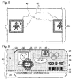
- FIG. 6 shows a use of the dashed line 23 with the window surfaces 25 for sealing a badge 28.
- the badge 28 consists of the substrate 5 (Fig. 1), the color field 9 and the indicia 8 (Fig. 1) on its surface 29 (Fig. 1) to be protected by the laminating film, and a field for a photograph 30 of the card holder having.
- the indicia 8 are general information about the issuer of the pass in a text field 31.
- the photograph 30 is glued in the field provided or directly on the substrate 5 and inserted in a labeling strip 32, for example, the name of the owner and his Identification number, here "123-B-10", inscribed.
- a piece of the laminating film is glued to the badge by the belt 23 so that the photograph 30 is visible through the window surface 25 and the inscription strip 32 is visible through the area 26.
- the text field 31 and the color field 9 are hidden by the opaque partial surfaces of the strip 24 of the laminating film. After sticking the badge 28 is trimmed so that no excess remains of laminating remain.
- Pieces of the laminating film are also used to secure the passport details, visas in a passport, banknotes, packages, etc. In the following, these applications are described using the example of "passport".
- the writing device 18 (FIG. 1) is moved by means of a coordinate control over the surface to be described of the layer composite 1 in order to produce in a predetermined screening the transparent spots 7 (FIG. 1) such that the indicia 8 underlying the laminating film, e.g. in the text field 31, and, if no special window area 25 is provided in the laminating film, the photograph 30 can be seen through the transparent areas of the layer composite 1.
- the energy beam 19 ( Figure 1) of the writing device 18 further individual information is inscribed in the area of the reflective strip 24 on the card 28 by destroying the metallic layer 6 ( Figure 1), e.g. alphanumeric characters 33, emblems 34, a bar code 35 or rasterized images.
- the transparent areas 7 FIG. 1
- the transparent areas 7 form a dot and / or line pattern which stands out in the invariable color of the surface 29 conspicuously from reflecting surface parts 36 (FIG. 1) of the layer composite 1.
- the transparent areas 7 also have shapes of the alphanumeric characters 33, the emblems 34, the bar code 35 and are visible in the color of the surface 29.
- the text 33 is generated above the color field 9.
- the rectangular transparent areas 7 and the reflective areas 7 of different widths separating the transparent areas 7 form the bar code 35, the rectangular transparent areas 7 representing lines and the reflective areas 36 separating spaces of the bar code 35.
- the serial number is the individual element which is to be coded visually and / or machine-readable after the lamination foil has been affixed.
- the decorative films whether used later as laminating films or packaging films, can be described with the patterns explained.
- One application is to label a packaging film with the logo or trademark of the product to be packaged.
- a multi-layer dielectric layer 3 e.g. from US 3,858,977 is known to read.
Description
- Die Erfindung bezieht sich auf eine Dekorfolie, ein Verfahren zum Beschriften der Dekorfolie und eine Verwendung der Dekorfolie gemäss dem Oberbegriff der Ansprüche 17 und 21.
- Solche Dekorfolien werden zum Sichern und zum Schutz von Beschriftungen, Photos und anderen Indicia auf Dokumenten, wie Pässen, Identitätskarten, Kreditkarten, Banknoten usw., oder zum Verpacken von Wertgegenständen verwendet.
- In der US 5,331,443 ist ein Verfahren beschrieben, wie eine frisch geprägte und mit einer Reflexionsschicht überzogene lichtbeugende Reliefstruktur durch eine Beschriftung individualisierbar ist. Die Reflexionsschicht wird mittels Laserstrahlen lokal entfernt und anschliessend mit einer Klebeschicht überzogen. Der Nachteil dieses Verfahrens liegt darin, dass vor der Fertigstellung des Schichtverbunds durch Auftragen der Klebeschicht die individuelle Beschriftung eingebracht werden muss.
- Es ist auch bekannt (US 2,590,906), dass ein mit einem Metall beschichtetes Dielektrikum ein Interferenzfilter bildet, das im Tageslicht brillante Interferenzfarben reflektiert. In der US 3 858 977 ist die Eignung von mehrschichtigen Interferenzfiltern als Echtheitsmerkmal für Dokumente beschrieben. Gemäss US 3,338,730 sind strukturierte, nicht Tageslicht beugende Oberflächen mit solchen Interferenzfiltem überzogen worden, um ein in den Interferenzfarben aufscheinendes, attraktives Verpackungsmaterial zu erhalten.
- Die WO 98/19869 beschreibt ein Verfahren zum Perforieren von Dokumenten mittels gebündeltem Laserlicht. Die Dichte der im Dokument hergestellten Löcher und deren Durchmesser werden durch ein Muster einer Vorlage bestimmt. Dazu tastet ein optischer Sensor die Vorlage ab und setzt die erkannten Grautöne der Vorlage in Dichte und Durchmesser der eingebrannten Löcher um. Damit lassen sich Bilder. Porträts oder Buchstabenbilder erzeugen, die in Durchsicht erkennbar und praktisch nicht verfälschbar sind. Anwendungen dieses Verfahrens sind im Aufsatz "Application of laser technology to introduce security features on security documents in order to reduce counterfeiting" von W. Hospel in Proceedings of SPIE, Vol. 3314, 28 - 30 January, 1998, Seiten 254 - 259 beschrieben.
- Im Aufsatz "Search for effective document security by 'inventioneering' " von J. D. Brongers in Proceedings of SPIE Vol. 3314, January, 1998, Seiten 29 - 38 werden mit dem intensiven, fein fokussierten Laserlicht Farbschichten auf der Oberfläche eines Substrats in vorgegebenem Muster aus einem Druckbild entfernt, ohne das Substrat selbst zu beschädigen.
- Die US 4'662'653 beschreibt eine optische Gitterstruktur aus spiegelnden ebenen Metallamellen. Die Metallamellen sind in einer Ebene periodisch angeordnet, die im vorbestimmten Abstand d parallel zu einer vollflächigen spiegelnden, ebenen metallischen Fläche ist. Die Metallamellen weisen eine Periode von 10 Mikrometer oder weniger auf. Die Metallamellen und die metallische Fläche sind mit Vorteil in ein transparentes Dielektrikum eingebettet und durch eine Schutzschicht aus dem gleichen dielektrischen Material geschützt. Durch die Schutzschicht einfallendes Licht wird durch die optische Gitterstruktur in die aktiven Beugungsordnungen gebeugt.
- Die EP 0 201 323 B1 beschreibt den Schichtaufbau von Kunststoffolien, die eingeprägte Hologramme mit transparenten Reflexionsschichten einschliessen. Die für den Schichtaufbau und die Reflexionsschicht geeignete Materialien sind in diesem Dokument zusammengestellt.
- Transparente Dielektrika mit einem sehr hohen Brechungsindex zur Erhöhung des Reflexionsvermögens bei Beugungsstrukturen sind aus der WO 99/47983 bekannt.
- Der Erfindung liegt die Aufgabe zugrunde, eine kostengünstige Dekorfolie zu schaffen, die sich zum Beschriften und zum Auflaminieren auf ein Dokument bzw. zum Verpacken eignet, ein Verfahren anzugeben, wie in die Dekorfolie Informationen eingebracht werden und eine Verwendung für die Dekorfolie anzugeben.
- Die genannte Aufgabe wird erfindungsgemäss durch die im Kennzeichen der Ansprüche 17 und 21 angegebenen Merkmale gelöst. Vorteilhafte Ausgestaltungen der Erfindung ergeben sich aus den abhängigen Ansprüchen.
- Ausführungsbeispiele der Erfindung sind in der Zeichnung dargestellt und werden im folgenden näher beschrieben.
- Es zeigen:
- Figur 1
- eine Dekorfolie auf einem Substrat im Querschnitt,
- Figur 2
- eine andere Ausführung der Dekorfolie im Querschnitt,
- Figur 3a
- ein Motiv in der Dekorfolie im Querschnitt,
- Figur 3b
- das Motiv in Draufsicht auf die Dekorfolie,
- Figur 4
- Ausführungen der Dekorfolie in Draufsicht,
- Figur 5
- ein Dekorfolienband in Draufsicht
und - Figur 6
- ein mit der Dekorfolie laminiertes Dokument.
- In der Figur 1 bedeutet 1 einen Schichtverbund für eine Dekorfolie, 2 eine Basisfolie, 3 eine dielektrische Schicht, 4 eine Deckschicht, 5 ein Substrat, 6 eine metallische Schicht, 7 eine transparente Stelle ohne metallische Schicht 6 sowie 8 Indicia und 9 ein Farbfeld auf dem Substrat 5. Das Substrat 5 ist wenigstens Teil eines Dokuments, wie Banknote, Personalausweis, Pass, Identitätskarte, Kreditkarte usw.
- Der Schichtverbund 1 ist auf einer transparenten Basisfolie 2 aufgebaut. Bei einer einfachen Ausführung des Schichtverbunds 1 ist die innenliegende Seite der Basisfolie 2 vollflächig mit einer dünnen Schicht 3 eines transparenten Dielektrikums überzogen. Anschliessend folgt auf der dielektrischen Schicht 3 wenigstens in Teilbereichen eine reflektierende metallische Schicht 6. Die metallische Schicht 6 kann direkt nur in den Teilbereichen aufgetragen sein oder zunächst vollflächig,
wobei anschliessend ausserhalb der Teilbereiche die metallische Schicht 6 wieder entfernt wird. Der Schichtverbund 1 wird als Dekorfolie fertiggestellt durch Abdecken der dielektrischen Schicht 3 bzw. metallischen Schicht 6 mit der Deckschicht 4. - Ist die Dekorfolie zum Auflaminieren auf ein Substrat 5 vorgesehen, weist das Material der Deckschicht 4 eine Klebefähigkeit auf. Der Schichtverbund 1 wird mit der Deckschicht 4 mit dem Substrat 5 in Kontakt gebracht und durch Aktivieren des Klebers der Deckschicht 4 mit dem Substrat 5 verbunden. Beispielsweise besteht die Deckschicht 4 aus einem Heisskleber, dessen Klebefähigkeit sich erst durch Erwärmen des Schichtverbunds 1 und des Substrats 5 auf eine Temperatur von über 100°C entwickelt. Solche Heisskleber sind auf Polyurethan- oder Polyäthylenbasis verfügbar. In einer anderen Ausführung des Schichtverbunds 1 ist das Material der Deckschicht 4 ein Kaltkleber, der durch Andrücken des Schichtverbunds 1 auf das Substrat 5 aktiviert wird. Der Einsatz eines Kaltkleber bedingt, dass die freie Oberfläche der Deckschicht 4 sofort nach dem Aufbringen des Kaltklebers mit einer hier nicht gezeigten Abziehfolie abzudecken ist. Die Abziehfolie muss vor dem Aufkleben des Schichtverbunds 1 auf das Substrat 5 entfernt werden. Für die Deckschicht 4 verwendbare Materialien sind in der EP 0 201 323 B1, im Abschnitt "adhesive layer" auf der Seite 13 erwähnt.
- Die Basisfolie 2 kann auf der dem Dielektrikum zugewandten Seite eine transparente Lackschicht 10 aufweisen, um bessere Haftung des Dielektrikums und/oder um eine leichtere mechanische Verformbarkeit der dem Dielektrikum zugewandten Oberfläche der Basisfolie 2 zu erhalten, wenn sich die Lackschicht 10 zum Abformen eines mikroskopisch feinen Reliefs eines Flächenmusters besser als die Basisfolie 2 eignet. Das Flächenmuster umfasst mosaikartig angeordnete Beugungselemente und andere Flächenelemente mit streuenden oder spiegelnden Eigenschaften oder ist ein Hologramm. Die Lackschicht 10 ist wenigstens etwa doppelt so dick wie die Profilhöhe der mikroskopisch feinen Reliefs des Flächenmusters aufgetragen; die Dicke der Lackschicht 10 liegt im Bereich von 150 nm bis 2 µm. Das Abformen des Reliefs kann vor oder nach dem Aufbringen der dielektrischen Schicht 3 oder auch erst in die metallische Schicht 6 erfolgen.
- Heisslaminierbare Dekorfolien weisen in einer Ausführung zwischen einer Lackschicht 10 und der Basisfolie 2 mit Vorteil eine in der Figur 1 durch eine gestrichelte Linie angedeutete, etwa 500 nm bis 1 µm starke Trennschicht 10' auf, um nach dem Auflaminieren der Dekorfolie auf das Substrat 5 die Basisfolie 2 abziehen zu können. Der auf dem Substrat 5 verbleibende Teil des Schichtverbundes 1 ist weniger als 20 µm stark.
- In einer anderen Ausführung enthält der Schichtverbund 1 zusätzlich einen transparenten Metallfilm 11 zwischen der Basisfolie 2 bzw. der Lackschicht 10 und der dielektrischen Schicht 3. Der Metallfilm 11 überdeckt die erste Grenzschicht 13 derart, dass die dielektrische Schicht 3 zwischen dem Metallfilm 11 und der metallischen Schicht 6 eingebettet ist.
- Transparentes Material ist optisch klar und lässt das ganze Spektrum des sichtbaren Lichts (= glasklares Material) oder nur gewisse Spektralbereiche desselben (= farbiges Material) durch.
- Als Basisfolie 2 eignen sich Folienbahnen aus Polyvinylchlorid (PVC), Polycarbonat (PC), Polyethylentheraphtalat (PETP), Polyäthylen (PE), Polypropylen (PP), Cellophan oder eine Folie aus einem anderen transparenten Kunststoff, die in Breiten von etwa 30 cm bis 120 cm im Handel erhältlich sind. Gemeinsam sind den Folien ihre hohe Transparenz und grosse Zugfestigkeit auch in geringen Schichtdicken. Typisch liegen die Schichtdicken dieser Folien, in Abhängigkeit vom Folienmaterial, im Bereich zwischen 200 µm und weniger als 9 µm. Der Brechungsindex nD dieser Materialien liegen im Wertebereich von 1,50 bis 1,60 bzw. diesem Bereich um wenige Zehntel unmittelbar benachbart. Eine gute Haftung zwischen der Basisfolie 2 und den übrigen Schichten des Schichtverbunds 1 ist unabdingbar.
- Die Lackschicht 10 wird auf der Basisfolie 2 in Form eines dünnflüssigen Lacks aufgetragen. Beispiele verschiedener transparenter Lacke sind in der eingangs erwähnten EP 0 201 323 B1, Seite 5, Abschnitt "Transparent hologram forming layer" aufgeführt, sowohl lösungsmittelhaltige als auch lösungsmittelfreie, z.B. mittels ultraviolettem Licht härtende, Lacke. Ein Rezept für einen Lack mit Lösungsmittel für die thermoplastische Lackschicht 10 ist auf der Seite 19, Zeile 15 der EP 0 201 323 B1 angegeben.
- Die dielektrische Schicht 3 weist in einer Ausführung einen im wesentlichen gleichmässigen Auftrag in der Stärke s auf, wobei die Stärke s höchstens 300 nm beträgt, typische Werte sind jedoch 50 nm bis 200 nm. Geeignete, im sichtbaren Teil des Spektrums elektromagnetischer Wellen transparente Dielektrika sind in der eingangs erwähnten EP 0 201 323 B1, Tabelle 1 erwähnt. Das ausgewählte Dielektrikum wird im Vakuum mittels Aufdampfen oder Sputtern auf die Basisfolie 2 bzw. auf die Lackschicht 10 aufgetragen. Bevorzugte transparente Dielektrika sind MgF2, ZnO, SiO, SiO2, TiO2 und ZnS sowie die sich durch einen sehr hohen Brechungsindex auszeichnenden, aus der WO 99/47983 bekannten chalkogeniden Substanzen, wie Ge30Sb10S60 (n= 2.25), As50Ge20Se30 (n= 2.95), Ge20Sb25Se55 (n= 3.11).Durch die Basisfolie 2 in den Schichtverbund 1 unter einem Einfallswinkel α eindringendes weisses Licht 12 wird an einer ersten Grenzfläche 13 zwischen der Basisfolie 2 bzw. Lackschicht 10 und dem Metallfilm 11 bzw. der dielektrischen Schicht 3 sowie an einer zweiten Grenzfläche 14 zwischen der dielektrischen Schicht 3 und der metallischen Schicht 6 bzw. der Deckschicht 4 teilweise reflektiert, wobei der Grad der Reflexion vom Sprung im Brechungsindex beim Übergang an jeder Grenzfläche 13, 14 und dem Einfallswinkel α bestimmt ist. Lichtstrahlen 15, die in die dielektrische Schicht 3 eingedrungen sind und an der zweiten Grenzfläche 14 reflektiert wurden, legen eine grössere Wegstrecke zurück wie Lichtwellen 16, die schon an der ersten Grenzfläche 13 gespiegelt wurden. Die Lichtstrahlen 15 und die Lichtwellen 16 weisen aufgrund des Weglängenunterschieds einen Phasenunterschied auf, wobei infolge von Interferenzeffekten ein reflektiertes Licht 17 aus den Lichtstrahlen 15 und den Lichtwellen 16 entsteht, bei dem bestimmte Wellenlängenbereiche aus dem Spektrum des weissen Lichts 12 ausgelöscht sind. Die Dekorfolie glänzt daher im Tageslicht in einer von der Dicke der dielektrischen Schicht 3 und dem Reflexionswinkel β, d.h. α = β, abhängigen Interferenzfarbe. Die Intensität der Interferenzfarbe des reflektierten Lichts 17 ist verstärkt, wenn die metallische Schicht 6 und/oder der Metallfilm 11 vorhanden ist.
- Anstelle dieser transparenten Dielektrika besteht in einer weiteren Ausführung die dielektrische Schicht 3 aus einem der für die Lackschicht 10 genannten Lacke. Da sich die Brechungsindices der Materialien für die Basisfolie 2 bzw. die Lackschicht 10 und für die Deckschicht 4 nur sehr wenig von der dielektrischen Schicht 3 unterscheiden, ist die Intensität der Interferenzfarben gering. Die dielektrische Schicht 3 ist daher vorzugsweise zwischen dem Metallfilm 11 und der metallischen Schicht 6 angeordnet.
- In einer anderen Ausführung des Schichtverbunds 1 ist für die Deckschicht 4 anstelle des Klebers dasselbe Material wie für die Lackschicht 10 aufgetragen. Eine solche Folie ist als Verpackungsfolie für exklusive Gegenstände und Geschenkartikel verwendbar. Auch die mit einem Heisskleber ausgerüsteten Dekorfolien sind zum Verpacken verwendbar. Deshalb bezeichnet "Dekorfolie" sowohl eine dekorative Laminierfolie als auch eine dekorative Verpackungsfolie.
- Das gegebenenfalls in die Lackschicht 10 eingeformte, mikroskopisch feine Relief des beugungsoptischen Flächenmusters beugt an der ersten und zweiten Grenzfläche 13, 14 das einfallende Licht 12 mit der Wellenlänge λ unter den durch die Wellenlänge λ und den jeweiligen Gitterparameter, wie Gittervektor, Reliefprofil, Spatialfrequenz f, Azimut usw., bestimmten Beugungswinkeln γ. Das an der ersten Grenzfläche 13 gebeugte Licht weist gegenüber dem an der zweiten Grenzfläche 14 gebeugten Licht einen Weglängenunterschied auf. Wegen der Interferenzeffekte kann das unter dem Beugungswinkel γ in der m-ten Ordnung gebeugte Licht mit der Wellenlänge λ ausgelöscht werden, so dass Teile des Flächenmusters statt in brillanten Farben in einer Mischfarbe oder gar grau bis schwarz erscheinen. Falls der Gittervektor in der Ebene des unter dem Winkel α einfallenden Lichts 12 liegt, ist der Beugungswinkel γ durch die Beziehung γ = ± arcsin[m·f·λ + sin(α)] bestimmt. Zur Vereinfachung der Darstellung in der Figur 1 sind Richtungsänderungen der Lichtstrahlen 12, 15, 16 infolge von Brechungseffekten nicht gezeigt.
- Die metallische Schicht 6 und der Metallfilm 11 bestehen aus einem Metall der bevorzugten Gruppe: Aluminium, Silber, Gold, Chrom, Kupfer und Tellur. Diese Metalle eignen sich zum Aufdampfen der metallischen Schicht 6 bzw. des Metallfilms 11 und sind im Schichtverbund 1 chemisch unempfindlich. Die metallische Schicht 6 soll einen Grossteil der einfallenden Lichtstrahlen 12 reflektieren. Die Dicke D der metallischen Schicht 6 beträgt daher mehr als 50 nm, vorzugsweise 50 nm bis 300 nm. Im Gegensatz dazu muss der Metallfilm 11 für einen Grossteil des einfallenden Lichts 12 transparent sein; der Metallfilm 11 weist daher eine Schichtdicke d im Wert von 50 nm oder weniger auf; ein typischer Bereich der Schichtdicke d ist 5 nm bis 15 nm. Die Schichtdicken D und d sind vom Metall und der Wellenlänge λ des einfallenden Lichts 12 bzw. 15 abhängig, wie dies in "Optical properties of thin solid films" von O. S. Heavens, Butterworths Scientific Publications, London (1955), Seiten 156 - 170 dargelegt ist. In einer Sonderausführung ist auch die Dicke D (Fig. 1) der metallischen Schicht 6 so gering, dass die metallische Schicht 6 so transparent wie der Metallfilm 11 ist. Die Reflektivität im Schichtverbund 1 ist höher als beim Schichtverbund 1 ohne Metallschichten 6, 11, jedoch geringer als bei der Dekorfolie mit einer vollständig reflektierenden metallischen Schicht 6. Der Schichtverbund 1 ist daher auf seiner ganzen Fläche farbig transparent und reflektiert farbiges Licht 17.
- Eine Schreibeinrichtung 18 umfasst eine gepulste Lichtquelle, z.B. Laser, Leuchtdiode usw., mit einer Fokussiereinrichtung kurzer Brennweite. Ein von der Lichtquelle kurzzeitig emittierter Energiestrahl 19 hoher Leistung wird mittels der Fokussiereinrichtung derart durch die Basisfolie 2 hindurch in den Schichtverbund 1 hinein gebündelt, dass sich der Fokus des Energiestrahls 19 und damit die höchste Leistungsdichte im Bereich der metallischen Schicht 6 befindet. Auf einer Achse des Energiestrahls 19 nimmt die Leistungsdichte ausserhalb des Fokus rasch ab. Die dünne metallischen Schicht 6 und ein allfällig vorhandener Metallfilm 11 werden lokal schnell über den Schmelzpunkt des Metalls hinaus erwärmt. Beim Abkühlen erstarrt das Metall an den Grenzflächen 13, 14 zu sehr feinen, vom Auge nicht sichtbaren Kügelchen. Der Energiestrahl 19 perforiert nur die Metallschichten 6, 11, nicht aber die anderen Schichten des Schichtverbunds 1, so dass der Schichtverbund 1 an der Perforation die transparente Stelle 7 aufweist. Im Fokus beträgt der Durchmesser des Energiestrahls 19 typisch einige 10 µm. Die Impulsdauer und die abgegebene Leistung des Energiestrahls 19 bestimmen den Durchmesser der mit einem Impuls erzeugten transparenten Stelle 7. Eine Vielzahl von Impulsen des Energiestrahls 19, appliziert an unmittelbar nebeneinander liegenden Orten, erzeugen die kreisrunde transparente Stelle 7 mit einer Abmessung bis 1 mm oder eine bis zu 1 mm breite, linienförmige transparente Stelle 7. Die Impulsdauer, die Leistung und die Wellenlänge des Energiestrahls 19 sind so zu wählen, dass der Energiestrahl 19 einerseits möglichst wenig Energie in der dielektrischen Schicht 3, in den Kunststoffschichten 2, 4, 10 und in den Indicia 8 bzw. dem Farbfeld 9 deponiert, so dass sich deren Erwärmung in Grenzen hält und keine Beschädigung des Schichtverbunds 1 bzw. des Substrats 5 auftritt, und anderseits vom Metall der Schichten 6, 11 stark absorbiert wird. Die Folienbahnen mit dem Schichtaufbau 1 sind mit dieser Einrichtung in den Teilflächen mit der metallischen Schicht 6 beschriftbar. Dazu werden die Folienbahnen auf einer Umrollanlage von einem Wickel abgerollt und auf dem andern wieder aufgerollt. Während des Umrollens wird die Foliebahn unter dem computergesteuerten, quer über die Folienbahn verschiebbaren Energiestrahl 19 hindurchgezogen und die transparenten Stellen 7 in einem vorbestimmten Muster im Schichtverbund 1 erzeugt.
- In der Ausführung der Dekorfolie gemäss Figur 2 weist der Schichtverbund 1 die dielektrische Schicht 3 auf, deren Stärke s in der Richtung z in einem Winkel θ (Fig. 4) zur Laufrichtung x (Fig. 4) der Dekorfolie mit einer Funktion F(z) moduliert ist. Der Winkel θ weist einen Wert im Bereich von 30° bis 90° auf. Die Funktion F(z) ist beispielsweise, wie in der Figur 2 gezeigt, periodisch, wobei eine in der Richtung z gemessene Periode p in der Grössenordnung von einigen Zentimetern bis Dezimetern liegt; vorzugsweise ist die Länge der Periode p aus dem Bereich 1 cm ≤ p ≤ 50 cm gewählt. Diese Modulation wird durch ein ungleichmässiges Aufdampfen des Materials für die dielektrischen Schicht 3 erhalten. Die Funktion F(z) ändert die Werte der Stärke s zwischen einem Minimalwert M und dem Maximalwert A. Zum Beispiel liegt der Minimalwert M im Bereich ≤ 50 nm, während sich der Bereich für den Maximalwert A von 100 nm bis 300 nm erstreckt. Die Stärke s variiert daher sehr langsam über die Fläche der Dekorfolie. Für die in der Darstellung der Figur 2 gezeigte Sägezahn - Funktion F(z) liegt der Gradient der Stärke s im Bereich von 2 nm/cm bis 250 nm/cm, wenn die vorgenannten Werte für den Minimalwert M, den Maximalwert A und für die Periode p angenommen werden. Für andere Funktionen F(z) ändert sich die Stärke s zwischen dem Minimalwert M und dem Maximalwert A mit einem maximalen Gradienten der Stärke s, der sich im gleichen Bereich wie bei der periodischen Sägezahn - Modulation bewegt.
- Da, wie oben ausgeführt, die Farbe des von der Dekorfolie reflektierten Lichts 17 (Fig. 1) von der Stärke s der dielektrischen Schicht 3 abhängt, ändert sich die Farbe des reflektierten Lichts 17 über die Fläche des Schichtverbunds 1 entsprechend der durch die Funktion F(z) bewirkten Modulation der Stärke s. Mit und ohne beugungsoptische Flächenmuster in der Basisfolie 2 bzw. Lackschicht 10 weist ein solcher Schichtverbund 1 ein auffallendes Aussehen auf. Ein besonders auffälliges Muster wird erhalten, falls nach dem Auftragen einer ersten, in der Richtung (z) modulierten dielektrischen Schicht 3 in einer zweiten Anlage auf diese erste Schicht 3 ein zweites Dielektrikum aus demselben oder einem anderen Material abgeschieden wird, wobei die Auftragsstärke des zweiten Dielektrikums z.B. quer zur Richtung z moduliert ist. In diesem Beispiel erscheint im reflektierten Licht 17 auf der Oberfläche der Dekorfolie ein netzförmiges, farbiges Muster.
- In einer in der Figur 3a gezeigten Ausführung der dielektrischen Schicht 3 ist die Modulation binär, d.h. die dielektrische Schicht 3 weist nur zwei Werte der Stärke s (Fig. 2) auf. Die dünnere Schicht in Hintergrundflächen 40 weist einen Wert der Stärke smin von weniger als 200 nm und die dickere Schicht in Motivflächen 41 einen Wert der Stärke smax im Bereich von 100 nm bis 300 nm auf, wobei die Stärke smax wenigstens um 25 nm dicker als die Stärke smin ist. In einem Spezialfall ist die Stärke smin = 0; d.h. die dielektrische Schicht 3 besteht aus den nicht zusammenhängenden Motivflächen 41, die durch die Hintergrundflächen 40 mit oder ohne metallische Schicht 6 getrennt sind. In einem Beispiel ist auf die gleichmässig aufgetragene dielektrische Schicht 3 ein aus Motivflächen 41 bestehendes Motiv aus dem gleichen oder einem anderen Dielektrikum so aufgetragen, dass die dielektrischen Schicht 3 die Stärke smax in den Motivflächen 41 des Motivs und die Stärke smin ausserhalb der Motivflächen 41 aufweist. Die Stärke s der dielektrische Schicht 3 ändert sich gemäss dem Motiv und ist daher mit dem Motiv moduliert. Beim Betrachten des Schichtverbunds 1 ist das Motiv durch die Basisfolie 2 hindurch sichtbar. Die Motivflächen 41 unterscheiden sich von den Hintergrundsflächen 40 durch eine andere Interferenzfarbe des reflektierten Lichts 17 (Fig. 1). Die Erzeugung der Motivflächen 41 erfolgt mit Vorteil durch Auftragen einer zusätzlichen Schicht des Dielektrikums, z.B. durch eine hier nicht gezeigte Maske hindurch, oder mittels eines an sich bekannten Druckverfahrens, wobei in den Motivflächen 41 vorzugsweise der oben erwähnte transparente Lack bis auf die erforderliche Stärke smax aufgetragen wird.
- Überlappen sich die Motivflächen 41, die nacheinander in verschiedenen Schichten mit demselben Dielektrikum oder mit verschiedenen Dielektrika aufgetragen sind, ergibt die Anordnung der Motivflächen 41 eine Stufenmodulation der aus dem Dielektrikum oder den Dielektrika bestehenden Schicht 3.
- Die Figur 3b zeigt in der Draufsicht die Struktur der dielektrischen Schicht 3, wobei die erhabenen Motivflächen 41 zeichnerisch gerastert dargestellten sind. Die Abmessungen der mittels eines Linienrasters zeichnerisch dargestellten Motivflächen 41 sind meist grösser als 0,3 mm, ausser bei gerasterten Bildern 42, deren Motivflächen 41 einen Punktraster mit einer Auflösung von bis zu 400 dpi (= 16 Pixel/mm) aufweisen. Werden Grauwerte der Bilder 42 durch die Dichte des Punktrasters dargestellt, sind schwarz-weiss Portraits als Vorlage für die Bilder 42 verwendbar. Die Motivflächen 41 und/oder die Bilder 42 bilden ein Muster 43. Zu erwähnen ist in diesem Zusammenhang die Tintenstrahldrucktechnik, mit der die Motivflächen 41 der gerasterten Bilder 42, Schriften und Linien nach einer in einem Computer in elektronischer Form gespeicherten Vorlage auf die dielektrische Schicht 3 übertragen werden.
- Es wird nun wieder auf Figur 1 Bezug genommen. Da die Schicht 6 infolge ihrer Schichtdicke D praktisch nicht mehr transparent ist, verdeckt der Schichtverbund 1 in den Teilflächen mit den metallischen Schichten 6 die unter dem Schichtverbund 1 liegenden Indicia 8 oder Farbfelder 9. Im Gegensatz dazu ist der Schichtverbund 1 in den übrigen Teilflächen, wo die transparente dielektrische Schicht 3 direkt an die Deckschicht 4 angrenzt, transparent. Die unter der transparenten Dekorfolie liegenden Indicia 8 oder Farbfelder 9 bzw. Oberfläche 29 des Substrats 5 sind gut sichtbar, sofern die Sichtbarkeit durch das farbige, reflektierte Licht 17 nicht gestört wird.
- Die Figur 4 zeigt einen Ausschnitt aus einer Folienbahn mit dem Schichtverbund 1 (Fig. 1), die sich in der Richtung x erstreckt. Die breite Dekorfolie wird nach dem Aufbringen der Deckschicht 4 (Fig. 2) bzw. der allfälligen Abziehfolie entlang den Linien 20, 21, 22 in Bänder 23 von vorbestimmter Breite geteilt und in den Verkehr gebracht.
- In der Darstellung der Figur 4 ist auf der linken Seite eine Ausführung der Dekorfolie gezeigt, bei der die dielektrische Schicht 3 (Fig. 1) eine möglichst gleichmässige Stärke s (Fig. 1) aufweist. In einer Ausführung des Bandes 23 weist die dielektrische Schicht 3 in einem Streifen 24 wenigstens an der zweiten Grenzfläche 14 (Fig. 1) die metallische Schicht 6 (Fig. 2) auf, während streifenförmige Areale 26, 26' des Schichtverbunds 1 transparent sind. In der Zeichnung der Figur 4 sind im Band 23 der mit einem groben Punktraster hervorgehobene Streifen 24, 24' und das Areal 26, 26' mit einer gestrichelten Linie zeichnerisch getrennt. In einer Ausführung weist der Streifen 24 in regelmässigen Abständen Fensterflächen 25 in der metallische Schicht 6 auf, in denen der Schichtverbund 1 transparent ist. In einer vorteilhaften Ausführung ist im Bereich der Fensterflächen 25 das mikroskopisch feine Relief des oben erwähnten Flächenmusters 27 eingeprägt, um die Fälschungssicherheit zu erhöhen. Das Flächenmuster 27 kann auch in an die Fensterflächen 25 angrenzende Zonen des Streifens 24 übergreifen.
- In einer anderen Ausführung der Dekorfolie, die in der Darstellung der Figur 4 auf der rechten Seite gezeigt ist, weist die dielektrischen Schicht 3 in der ausgezeichneten Richtung z die periodische Modulation der Stärke s auf. Das im reflektierten Licht verschieden farbig aufscheinende Streifenmuster ist in der Darstellung der Figur 4 mittels streifenförmigen Flächen, die alternierend einen dichten Raster und einen groben Raster bzw. keinen Raster aufweisen, mit zeichnerischen Mitteln hervorgehoben. In den Arealen 26' zwischen der Linie 21 bzw. 22 und der nächst gelegenen gestrichelten Linie weist die dielektrische Schicht 3 keinen Metallbelag auf und das Areal 26' ist transparent. Der grobe Raster im Streifen 24' zwischen der Linie 22 und der links davon gelegenen gestrichelten Linie symbolisiert das Vorhandensein der metallischen Schicht 6, so dass im Streifen 24' der Schichtverbund 1 undurchsichtig ist.
- In einer weiteren Ausführung des Schichtverbunds 1 ist die dielektrische Schicht 3 vollflächig wenigstens mit der metallischen Schicht 6 abgedeckt, so dass die ganze Dekorfolie intensiv farbig jedoch nicht transparent ist. Je nach Verwendungszweck wird die Dekorfolie in der Breite unzertrennt oder in Bänder 23 unterschiedlichster Breite zerteilt in den Verkehr gebracht.
- Die Figur 5 zeigt einen Ausschnitt des Bands 23 mit Blick auf die Basisfolie 2 (Fig. 3a). Im reflektierten Licht 17 (Fig. 1) hebt sich das Muster 43 wegen der Modulation der Stärke s (Fig. 2) der dielektrischen Schicht 3 (Fig. 3a) in einer anderen Interferenzfarbe von der Interferenzfarbe der Hintergrundflächen 40 in und um das Muster 43 ab. Das in der Figur 3b gezeigte Motiv 43 wiederholt sich beispielsweise in einem regelmässigen Abstand.
- In der Figur 6 ist eine Verwendung des gestrichelt gezeichneten Bandes 23 mit den Fensterflächen 25 zum Versiegeln eines Ausweises 28 gezeigt. Der Ausweis 28 besteht aus dem Substrat 5 (Fig. 1), das auf seiner mit der Laminierfolie zu schützenden Oberfläche 29 (Fig. 1) das Farbfeld 9 und die Indicia 8 (Fig. 1) und ein Feld für eine Photographie 30 des Ausweisinhabers aufweist. Die Indicia 8 sind allgemeine Angaben über den Herausgeber des Ausweises in einem Textfeld 31. Bei der Abgabe des Ausweises wird die Photographie 30 in das dafür vorgesehene Feld eingeklebt oder direkt auf das Substrat 5 eingebracht und in einem Beschriftungsstreifen 32 beispielsweise der Name des Inhabers und seine Identifikationsnummer, hier "123-B-10", eingeschrieben. Um ein nachträgliches Verändern des Ausweises 28 zu verhindern, wird ein Stück der Laminierfolie von dem Band 23 so auf den Ausweis geklebt, dass die Photographie 30 durch die Fensterfläche 25 hindurch und der Beschriftungsstreifen 32 durch das Areal 26 hindurch sichtbar sind. Das Textfeld 31 und das Farbfeld 9 sind durch die undurchsichtigen Teilflächen des Streifens 24 der Laminierfolie verdeckt. Nach dem Aufkleben wird der Ausweis 28 so beschnitten, dass keine überstehenden Reste der Laminierfolie verbleiben.
- Stücke der Laminierfolie finden auch Verwendung zum Sichern der Individualien eines Passes, von Visa in einem Pass, der Banknoten, der Verpackungen usw. Im folgenden sind diese Anwendungen anhand des Beispiels "Ausweis" beschrieben.
- Die Schreibeinrichtung 18 (Fig. 1) wird mittels einer Koordinatensteuerung über die zu beschreibende Fläche des Schichtverbunds 1 verschoben, um in einer vorbestimmten Rasterung die transparenten Stellen 7 (Fig. 1) so zu erzeugen, dass die unter der Laminierfolie liegenden Indicia 8, z.B. im Textfeld 31, und, wenn in der Laminierfolie keine spezielle Fensterfläche 25 vorgesehen ist, die Photographie 30 durch die transparenten Stellen des Schichtverbunds 1 hindurch sichtbar sind.
- Mit Vorteil werden mit dem Energiestrahl 19 (Fig. 1) der Schreibeinrichtung 18 auch weitere individuelle Informationen im Gebiet des reflektierenden Streifens 24 auf dem Ausweis 28 durch Zerstören der metallischen Schicht 6 (Fig. 1) eingeschrieben, wie z.B. alphanumerische Zeichen 33, Embleme 34, ein Strichkode 35 oder gerasterte Bilder. Durch die transparenten Stellen 7 (Fig. 1) hindurch ist die Farbe der darunterliegenden Oberfläche 29 zu erkennen. Die transparenten Stellen 7 bilden ein Punkt- und/oder Linienmuster, das sich in der unveränderlichen Farbe der Oberfläche 29 auffällig von reflektierenden Flächenteilen 36 (Fig. 1) des Schichtverbunds 1 abhebt. Anstelle des Punkt- und/oder Linienmusters weisen die transparenten Stellen 7 auch Formen der alphanumerischen Zeichen 33, der Embleme 34, des Strichkodes 35 auf und sind in der Farbe der Oberfläche 29 sichtbar. Im gezeigten Beispiel ist der Text 33, die Identifikationsnummer "123-B-10" aus dem Beschriftungsstreifen 32, über dem Farbfeld 9 erzeugt. In einem anderen Beispiel bilden die rechteckigen transparenten Stellen 7 und die die transparenten Stellen 7 trennenden, reflektierenden Flächenteile 36 unterschiedlicher Breite den Strichkode 35, wobei die rechteckigen transparenten Stellen 7 Striche und die reflektierenden Flächenteile 36 trennende Abstände des Strichkodes 35 darstellen. Bei der Banknote ist die Serienummer das individuelle Element, das nach dem Aufkleben der Laminierfolie kodiert visuell und/oder maschinell lesbar einzuschreiben ist.
- Die Schreibeinrichtung 18 ist in einer anderen Ausführung mit der aus der eingangs erwähnten WO 98/19869 bekannten Vorrichtung ausgerüstet und ist in der Lage, eine Bildvorlage abzulesen, sie in kleine, im Raster angeordnete Bildelemente (= Pixel) zu zerlegen und im Schichtverbund 1 in der metallischen Schicht 6 im gleichen Raster transparente Stellen 7 in Form einer Kreisfläche so zu erzeugen, dass die Bildvorlage in dem Schichtverbund 1 abgebildet ist. Grauwerte der Pixel werden durch verschieden grosse Durchmesser der transparenten Kreisflächen wiedergegeben. Auflösungen bis zu 400 dpi (= 16 Pixel pro mm) oder mehr sind erreichbar.
- Beispielsweise enthält die Laminierfolie zusätzlich das beugungsoptische Flächenmuster 27 in Form einer Guilloche im Bereich der Fensterfläche 25. Da die Fensterfläche 25 mit der Guilloche nie genau auf dem Feld für die Photographie plaziert ist, ist ein Vertauschen der Photographie 30 (im Rahmen eines Fälschungsversuches) an einem Bruch in der Linienführung der Guilloche erkennbar. Zusätzlich weist in einer Ausführung die Laminierfolie das mittels der Modulation der Stärke s (Fig. 2) der dielektrischen Schicht 3 erzeugte Muster 43 und/oder die periodische Modulation mit einem Streifen- oder Netzmuster auf.
- Auf der oben erwähnten Umrollanlage sind die Dekorfolien, ob später als Laminierfolien oder Verpackungsfolien verwendet, mit den erläuterten Mustern beschreibbar. Eine Anwendung ist das Beschriften einer Verpackungsfolie mit dem Logo oder mit dem Warenzeichen des zu verpackenden Produkts.
- Ohne von der erfinderischen Idee abzuweichen, ist in der obigen Beschreibung anstelle der dielektrischen Schicht 3 (Fig. 1) aus einem einzigen Dielektrikum auch eine aus mehreren Lagen bestehende dielektrische Schicht 3, wie sie z.B. aus der US 3,858,977 bekannt ist, mitzulesen.
Claims (21)
- Dekorfolie in Form eines Schichtverbunds (1), der wenigstens eine transparente Basisfolie (2), eine transparente Deckschicht (4), eine zwischen der Basisfolie (2) und der Deckschicht (4) angeordnete, transparente dielektrische Schicht (3) umfasst
dadurch gekennzeichnet,
dass zwischen der dielektrischen Schicht (3) und der Deckschicht (4) wenigstens in reflektierenden Flächenteilen (24; 24'; 36) eine metallische Schicht (6) angeordnet ist und dass zwischen der dielektrischen Schicht (3) und der Basisfolie (2) eine erste Grenzschicht (13) vorhanden ist, in der sich der Brechungsindex sprunghaft ändert. - Dekorfolie nach Anspruch 1,
dadurch gekennzeichnet,
dass die Basisfolie (2) auf der dem Dielektrikum zugewandten Seite eine zusätzlich aufgetragene, transparente thermoplastische Lackschicht (10) aufweist. - Dekorfolie nach Anspruch 2
dadurch gekennzeichnet,
dass zwischen der Basisfolie (2) und der transparenten thermoplastischen Lackschicht (10) eine 0,5 µm bis 1 µm starke Trennschicht (10') angeordnet ist. - Dekorfolie nach Anspruch 2 oder 3
dadurch gekennzeichnet,
dass wenigstens in den Bereichen der metallischen Schicht (6) zwischen der dielektrischen Schicht (3) und der Lackschicht (10) ein Metallfilm (11) angeordnet ist. - Dekorfolie nach Anspruch 1
dadurch gekennzeichnet,
dass wenigstens in den Bereichen der metallischen Schicht (6) zwischen der dielektrischen Schicht (3) und der Basisfolie (2) ein Metallfilm (11) angeordnet ist. - Dekorfolie nach Anspruch 4 oder 5
dadurch gekennzeichnet,
dass der Metallfilm (11) eine Transparenz von wenigstens 50 % aufweist. - Dekorfolie nach einem der Ansprüche 4 bis 6
dadurch gekennzeichnet,
dass der Metallfilm (11) aus einem Metall der Gruppe Aluminium, Silber, Gold, Chrom, Kupfer und Tellur besteht. - Dekorfolie nach einem der Ansprüche 1 bis 7
dadurch gekennzeichnet,
dass die metallische Schicht (6) aus einem Metall der Gruppe Aluminium, Silber, Gold, Chrom, Kupfer und Tellur besteht. - Dekorfolie nach einem der Ansprüche 1 bis 8,
dadurch gekennzeichnet,
dass die Stärke (s) der dielektrischen Schicht (3) wenigstens in einer Richtung (z) über die Fläche des Schichtverbunds (1) periodisch moduliert ist. - Dekorfolie nach einem der Ansprüche 1 bis 9,
dadurch gekennzeichnet,
dass die Stärke (s) der dielektrischen Schicht (3) eine Funktion des Ortes ist und sich über die Fläche des Schichtverbunds (1) mit einem Gradienten der Stärke (s) von 2 nm/cm bis 250 nm/cm ändert. - Dekorfolie nach einem der Ansprüche 1 bis 10,
dadurch gekennzeichnet,
dass die dielektrische Schicht (3) in Teilbereichen eine Licht (12) beugende, mikroskopisch feine Reliefstruktur eines Flächenmusters (27) an der der Basisfolie (2) zugewandten ersten Grenzfläche (13) und/oder an einer der Deckschicht (4) zugewandten zweiten Grenzfläche (14) aufweist. - Dekorfolie nach einem der Ansprüche 1 bis 11,
dadurch gekennzeichnet,
dass die dielektrischen Schicht (3) aus einem der transparenten Dielektrika der Gruppe MgF2, ZnO, TiO2, SiO, SiO2, ZnS oder einer chalkogeniden Substanz besteht. - Dekorfolie nach einem der Ansprüche 1 bis 11,
dadurch gekennzeichnet,
dass die dielektrischen Schicht (3) aus mehreren Lagen mit verschiedenen transparenten Dielektrika besteht. - Dekorfolie nach Anspruch 12 oder 13,
dadurch gekennzeichnet,
dass die Stärke (s) der dielektrischen Schicht (3) weniger als 300 nm beträgt. - Dekorfolie nach einem der Ansprüche 1 bis 14,
dadurch gekennzeichnet,
dass eine zweite Grenzfäche (14) zwischen der dielektrischen Schicht (3) und der Deckschicht (4) Stellen (7; 25; 26; 26') ohne metallische Schicht (6) aufweist und dass der Schichtverbund (1) an diesen Stellen (7; 25; 26; 26'), die einen Raster, ein Punkt- und/oder Linienmuster in Form von alphanumerischen Zeichen (33) und Emblemen (34) oder Fensterflächen (25) bilden, transparent ist. - Dekorfolie nach einem der Ansprüche 1 bis 15
dadurch gekennzeichnet,
dass das Material der Deckschicht (4) eine Klebefähigkeit aufweist, um den Schichtverbund (1) mittels der Deckschicht (4) mit einem Substrat (5) zu verbinden. - Verfahren zum Beschriften von Dekorfolien nach einem der Ansprüche 1 bis 16, dadurch gekennzeichnet, dass mittels gepulsten Energiestrahlen (19) im Schichtverbund (1) angeordnete, sich im Kontakt mit der dielektrischen Schicht (3) befindliche Metallschichten (6; 11) ohne eine weitere Beschädigung des Schichtverbunds (1) durch Verdampfen des Metalls im Bereich der Energiestrahlen (19) lokal perforiert werden, wobei im Schichtverbund (1) durch die Perforation der Metallschichten (6, 11) transparente Stellen (7) erzeugt werden.
- Verfahren nach Anspruch 17, dadurch gekennzeichnet, dass die im Kontakt mit der dielektrischen Schicht (3) befindlichen Metallschichten (6; 11) in einem Punkt- oder Linienraster perforiert werden, wobei die Dichte des Punkt- oder Linienrasters aufgrund eines vorgegebenen Musters lokal verändert wird.
- Verfahren nach Anspruch 17 oder 18, dadurch gekennzeichnet, dass die transparenten Stellen (7) bzw. die verbleibenden reflektierenden Flächenteile (36) in Form von alphanumerischen Zeichen (33) erzeugt werden.
- Verfahren nach einem der Ansprüche 17 bis 19, dadurch gekennzeichnet, dass die Metallschichten (6; 11) der Dekorfolie erst nach dem Aufkleben des Schichtverbunds (1) auf eine Indicia (8) tragende Oberfläche (29) eines Ausweises (28) lokal perforiert werden.
- Verwendung der Dekorfolie nach Anspruch 16
dadurch gekennzeichnet,
dass zum Versiegeln einer zu schützenden Oberfläche (29) des Substrats (5) die Deckschicht (4) des Schichtverbunds (1) mit dem Substrat (5) verbunden ist und dass das Substrat (5) ein Ausweis (28) ist.
Applications Claiming Priority (3)
| Application Number | Priority Date | Filing Date | Title |
|---|---|---|---|
| DE10064616A DE10064616C2 (de) | 2000-12-22 | 2000-12-22 | Dekorfolie und Verfahren zum Beschriften der Dekorfolie |
| DE10064616 | 2000-12-22 | ||
| PCT/EP2001/014970 WO2002051646A1 (de) | 2000-12-22 | 2001-12-18 | Dekorfolie |
Publications (2)
| Publication Number | Publication Date |
|---|---|
| EP1343639A1 EP1343639A1 (de) | 2003-09-17 |
| EP1343639B1 true EP1343639B1 (de) | 2006-07-19 |
Family
ID=7668696
Family Applications (1)
| Application Number | Title | Priority Date | Filing Date |
|---|---|---|---|
| EP01272028A Expired - Lifetime EP1343639B1 (de) | 2000-12-22 | 2001-12-18 | Dekorfolie |
Country Status (12)
| Country | Link |
|---|---|
| US (1) | US7078090B2 (de) |
| EP (1) | EP1343639B1 (de) |
| JP (1) | JP2004525785A (de) |
| AT (1) | ATE333382T1 (de) |
| CZ (1) | CZ298454B6 (de) |
| DE (2) | DE10064616C2 (de) |
| DK (1) | DK1343639T3 (de) |
| ES (1) | ES2269304T3 (de) |
| PL (1) | PL202500B1 (de) |
| PT (1) | PT1343639E (de) |
| TW (1) | TW536487B (de) |
| WO (1) | WO2002051646A1 (de) |
Cited By (1)
| Publication number | Priority date | Publication date | Assignee | Title |
|---|---|---|---|---|
| EP2159071B1 (de) | 2008-08-25 | 2015-12-09 | Hueck Folien Ges.m.b.H. | Sicherheitselement, das ohne Hilfsmittel verifiziert werden kann |
Families Citing this family (80)
| Publication number | Priority date | Publication date | Assignee | Title |
|---|---|---|---|---|
| US7667895B2 (en) * | 1999-07-08 | 2010-02-23 | Jds Uniphase Corporation | Patterned structures with optically variable effects |
| AT413360B (de) | 2002-08-06 | 2006-02-15 | Hueck Folien Gmbh | Verfahren zur herstellung von fälschungssicheren identifikationsmerkmalen |
| CN101164797B (zh) * | 2003-07-14 | 2012-07-18 | Jds尤尼费斯公司 | 防伪线 |
| US7476327B2 (en) * | 2004-05-04 | 2009-01-13 | Idc, Llc | Method of manufacture for microelectromechanical devices |
| JP4930745B2 (ja) * | 2004-07-12 | 2012-05-16 | 大日本印刷株式会社 | レ−ザ−印字用多層積層フィルム |
| US7304784B2 (en) * | 2004-09-27 | 2007-12-04 | Idc, Llc | Reflective display device having viewable display on both sides |
| US7372613B2 (en) | 2004-09-27 | 2008-05-13 | Idc, Llc | Method and device for multistate interferometric light modulation |
| US7583429B2 (en) | 2004-09-27 | 2009-09-01 | Idc, Llc | Ornamental display device |
| US7302157B2 (en) * | 2004-09-27 | 2007-11-27 | Idc, Llc | System and method for multi-level brightness in interferometric modulation |
| US7420725B2 (en) | 2004-09-27 | 2008-09-02 | Idc, Llc | Device having a conductive light absorbing mask and method for fabricating same |
| US7130104B2 (en) * | 2004-09-27 | 2006-10-31 | Idc, Llc | Methods and devices for inhibiting tilting of a mirror in an interferometric modulator |
| US7630119B2 (en) * | 2004-09-27 | 2009-12-08 | Qualcomm Mems Technologies, Inc. | Apparatus and method for reducing slippage between structures in an interferometric modulator |
| US7936497B2 (en) | 2004-09-27 | 2011-05-03 | Qualcomm Mems Technologies, Inc. | MEMS device having deformable membrane characterized by mechanical persistence |
| US7564612B2 (en) * | 2004-09-27 | 2009-07-21 | Idc, Llc | Photonic MEMS and structures |
| US7289259B2 (en) * | 2004-09-27 | 2007-10-30 | Idc, Llc | Conductive bus structure for interferometric modulator array |
| US8008736B2 (en) | 2004-09-27 | 2011-08-30 | Qualcomm Mems Technologies, Inc. | Analog interferometric modulator device |
| US7527995B2 (en) | 2004-09-27 | 2009-05-05 | Qualcomm Mems Technologies, Inc. | Method of making prestructure for MEMS systems |
| US7944599B2 (en) * | 2004-09-27 | 2011-05-17 | Qualcomm Mems Technologies, Inc. | Electromechanical device with optical function separated from mechanical and electrical function |
| DE102004061635A1 (de) † | 2004-12-17 | 2006-07-06 | Giesecke & Devrient Gmbh | Kartenförmiger Datenträger |
| DE102005021514B4 (de) * | 2005-05-10 | 2020-10-29 | Giesecke+Devrient Currency Technology Gmbh | Sicherheitselement und Verfahren zu seiner Herstellung |
| US7884989B2 (en) * | 2005-05-27 | 2011-02-08 | Qualcomm Mems Technologies, Inc. | White interferometric modulators and methods for forming the same |
| US20070007324A1 (en) * | 2005-07-06 | 2007-01-11 | Lynn Weddington | Gift wrap kit, methods and apparatus |
| US7916980B2 (en) | 2006-01-13 | 2011-03-29 | Qualcomm Mems Technologies, Inc. | Interconnect structure for MEMS device |
| US7550810B2 (en) * | 2006-02-23 | 2009-06-23 | Qualcomm Mems Technologies, Inc. | MEMS device having a layer movable at asymmetric rates |
| US7649671B2 (en) | 2006-06-01 | 2010-01-19 | Qualcomm Mems Technologies, Inc. | Analog interferometric modulator device with electrostatic actuation and release |
| US7835061B2 (en) | 2006-06-28 | 2010-11-16 | Qualcomm Mems Technologies, Inc. | Support structures for free-standing electromechanical devices |
| US7527998B2 (en) | 2006-06-30 | 2009-05-05 | Qualcomm Mems Technologies, Inc. | Method of manufacturing MEMS devices providing air gap control |
| DE102006034854A1 (de) * | 2006-07-25 | 2008-01-31 | Ovd Kinegram Ag | Verfahren zur Erzeugen einer Lasermarkierung in einem Sicherheitsdokument sowie derartiges Sicherheitsdokument |
| US8120854B2 (en) * | 2006-12-28 | 2012-02-21 | 3M Innovative Properties Company | Interference films having acrylamide layer and method of making same |
| US8289579B2 (en) | 2007-01-29 | 2012-10-16 | Hewlett-Packard Development Company, L.P. | Variable guilloche and method |
| US8115987B2 (en) | 2007-02-01 | 2012-02-14 | Qualcomm Mems Technologies, Inc. | Modulating the intensity of light from an interferometric reflector |
| US7742220B2 (en) * | 2007-03-28 | 2010-06-22 | Qualcomm Mems Technologies, Inc. | Microelectromechanical device and method utilizing conducting layers separated by stops |
| US7643202B2 (en) * | 2007-05-09 | 2010-01-05 | Qualcomm Mems Technologies, Inc. | Microelectromechanical system having a dielectric movable membrane and a mirror |
| US7715085B2 (en) * | 2007-05-09 | 2010-05-11 | Qualcomm Mems Technologies, Inc. | Electromechanical system having a dielectric movable membrane and a mirror |
| US7719752B2 (en) | 2007-05-11 | 2010-05-18 | Qualcomm Mems Technologies, Inc. | MEMS structures, methods of fabricating MEMS components on separate substrates and assembly of same |
| DE102007025866B4 (de) | 2007-06-01 | 2012-08-30 | Giesecke & Devrient Gmbh | Datenträger mit Sicherheitskennzeichnung |
| US7782517B2 (en) * | 2007-06-21 | 2010-08-24 | Qualcomm Mems Technologies, Inc. | Infrared and dual mode displays |
| US7630121B2 (en) | 2007-07-02 | 2009-12-08 | Qualcomm Mems Technologies, Inc. | Electromechanical device with optical function separated from mechanical and electrical function |
| NL2000782C2 (nl) † | 2007-07-26 | 2009-02-05 | Sdu Identification Bv | Kaart met metaalfolie laag voorzien van opening. |
| CN101809471B (zh) | 2007-07-31 | 2013-12-25 | 高通Mems科技公司 | 用于增强干涉式调制器的色彩偏移的装置 |
| US7847999B2 (en) * | 2007-09-14 | 2010-12-07 | Qualcomm Mems Technologies, Inc. | Interferometric modulator display devices |
| US7773286B2 (en) * | 2007-09-14 | 2010-08-10 | Qualcomm Mems Technologies, Inc. | Periodic dimple array |
| US7848003B2 (en) * | 2007-09-17 | 2010-12-07 | Qualcomm Mems Technologies, Inc. | Semi-transparent/transflective lighted interferometric devices |
| JP5209727B2 (ja) * | 2007-10-19 | 2013-06-12 | クォルコム・メムズ・テクノロジーズ・インコーポレーテッド | 一体型光起電力デバイスを有するディスプレイ |
| US8058549B2 (en) | 2007-10-19 | 2011-11-15 | Qualcomm Mems Technologies, Inc. | Photovoltaic devices with integrated color interferometric film stacks |
| GB2456500B (en) | 2007-10-23 | 2011-12-28 | Rue De Int Ltd | Improvements in security elements |
| EP2203765A1 (de) | 2007-10-23 | 2010-07-07 | Qualcomm Mems Technologies, Inc. | Auf mems basierende vorrichtungen mit einstellbarer durchlässigkeit |
| DE102008012419A1 (de) † | 2007-10-31 | 2009-05-07 | Bundesdruckerei Gmbh | Polymerschichtverbund für ein Sicherheits- und/oder Wertdokument, Verfahren zu dessen Herstellung sowie Sicherheits- und/oder Wertdokument |
| US8941631B2 (en) | 2007-11-16 | 2015-01-27 | Qualcomm Mems Technologies, Inc. | Simultaneous light collection and illumination on an active display |
| US7715079B2 (en) * | 2007-12-07 | 2010-05-11 | Qualcomm Mems Technologies, Inc. | MEMS devices requiring no mechanical support |
| JP2011507306A (ja) * | 2007-12-17 | 2011-03-03 | クォルコム・メムズ・テクノロジーズ・インコーポレーテッド | 干渉裏側マスクを有する光起電力装置 |
| US8164821B2 (en) * | 2008-02-22 | 2012-04-24 | Qualcomm Mems Technologies, Inc. | Microelectromechanical device with thermal expansion balancing layer or stiffening layer |
| US7944604B2 (en) | 2008-03-07 | 2011-05-17 | Qualcomm Mems Technologies, Inc. | Interferometric modulator in transmission mode |
| US7612933B2 (en) | 2008-03-27 | 2009-11-03 | Qualcomm Mems Technologies, Inc. | Microelectromechanical device with spacing layer |
| US7898723B2 (en) * | 2008-04-02 | 2011-03-01 | Qualcomm Mems Technologies, Inc. | Microelectromechanical systems display element with photovoltaic structure |
| US7969638B2 (en) * | 2008-04-10 | 2011-06-28 | Qualcomm Mems Technologies, Inc. | Device having thin black mask and method of fabricating the same |
| US8023191B2 (en) * | 2008-05-07 | 2011-09-20 | Qualcomm Mems Technologies, Inc. | Printable static interferometric images |
| US7768690B2 (en) * | 2008-06-25 | 2010-08-03 | Qualcomm Mems Technologies, Inc. | Backlight displays |
| US7746539B2 (en) * | 2008-06-25 | 2010-06-29 | Qualcomm Mems Technologies, Inc. | Method for packing a display device and the device obtained thereof |
| US8023167B2 (en) | 2008-06-25 | 2011-09-20 | Qualcomm Mems Technologies, Inc. | Backlight displays |
| US7859740B2 (en) * | 2008-07-11 | 2010-12-28 | Qualcomm Mems Technologies, Inc. | Stiction mitigation with integrated mech micro-cantilevers through vertical stress gradient control |
| US7855826B2 (en) * | 2008-08-12 | 2010-12-21 | Qualcomm Mems Technologies, Inc. | Method and apparatus to reduce or eliminate stiction and image retention in interferometric modulator devices |
| US8358266B2 (en) | 2008-09-02 | 2013-01-22 | Qualcomm Mems Technologies, Inc. | Light turning device with prismatic light turning features |
| EP2230539B1 (de) * | 2009-03-19 | 2019-12-04 | Viavi Solutions Inc. | Ausformung einer Abstandsschicht in einem Interferenzfilter |
| US8270056B2 (en) | 2009-03-23 | 2012-09-18 | Qualcomm Mems Technologies, Inc. | Display device with openings between sub-pixels and method of making same |
| RU2406152C1 (ru) * | 2009-04-28 | 2010-12-10 | Общество С Ограниченной Ответственностью "Новые Энергетические Технологии" | Защитный элемент для проверки подлинности объекта защиты и способ проверки подлинности |
| US9121979B2 (en) | 2009-05-29 | 2015-09-01 | Qualcomm Mems Technologies, Inc. | Illumination devices and methods of fabrication thereof |
| US8270062B2 (en) * | 2009-09-17 | 2012-09-18 | Qualcomm Mems Technologies, Inc. | Display device with at least one movable stop element |
| US8488228B2 (en) | 2009-09-28 | 2013-07-16 | Qualcomm Mems Technologies, Inc. | Interferometric display with interferometric reflector |
| EP2508922B2 (de) | 2009-12-01 | 2023-08-16 | Toppan Printing Co., Ltd. | Anzeigeelement und etikettierter artikel |
| KR20130100232A (ko) | 2010-04-09 | 2013-09-10 | 퀄컴 엠이엠에스 테크놀로지스, 인크. | 전기 기계 디바이스의 기계층 및 그 형성 방법 |
| DE102010019194A1 (de) † | 2010-05-04 | 2011-11-10 | Giesecke & Devrient Gmbh | Wertdokument mit Ausnehmung |
| JP2013544370A (ja) | 2010-08-17 | 2013-12-12 | クォルコム・メムズ・テクノロジーズ・インコーポレーテッド | 干渉ディスプレイデバイスの電荷中性電極の作動及び較正 |
| US9057872B2 (en) | 2010-08-31 | 2015-06-16 | Qualcomm Mems Technologies, Inc. | Dielectric enhanced mirror for IMOD display |
| US9134527B2 (en) | 2011-04-04 | 2015-09-15 | Qualcomm Mems Technologies, Inc. | Pixel via and methods of forming the same |
| US8963159B2 (en) | 2011-04-04 | 2015-02-24 | Qualcomm Mems Technologies, Inc. | Pixel via and methods of forming the same |
| US8659816B2 (en) | 2011-04-25 | 2014-02-25 | Qualcomm Mems Technologies, Inc. | Mechanical layer and methods of making the same |
| US8736939B2 (en) | 2011-11-04 | 2014-05-27 | Qualcomm Mems Technologies, Inc. | Matching layer thin-films for an electromechanical systems reflective display device |
| DE102015015730A1 (de) | 2015-09-28 | 2017-03-30 | Giesecke & Devrient Gmbh | Verpackung, Abdeckfolie und Verwendung einer Folie als Abdeckfolie |
| CN107041068B (zh) * | 2016-02-04 | 2019-10-25 | 毅嘉科技股份有限公司 | 电路板结构及其制造方法 |
Family Cites Families (23)
| Publication number | Priority date | Publication date | Assignee | Title |
|---|---|---|---|---|
| US2590906A (en) | 1946-11-22 | 1952-04-01 | Farrand Optical Co Inc | Reflection interference filter |
| US3338730A (en) * | 1964-02-18 | 1967-08-29 | Little Inc A | Method of treating reflective surfaces to make them multihued and resulting product |
| US3858977A (en) * | 1972-01-18 | 1975-01-07 | Canadian Patents Dev | Optical interference authenticating means |
| US4094575A (en) * | 1976-04-30 | 1978-06-13 | Minnesota Mining And Manufacturing Company | Holographic article and process for making same |
| CH661368A5 (de) * | 1984-01-03 | 1987-07-15 | Landis & Gyr Ag | Beugungsoptisches sicherheitselement. |
| CA1232068A (en) | 1984-06-08 | 1988-01-26 | National Research Council Of Canada | Form depicting, optical interference authenticating device |
| JPS6119350A (ja) | 1984-07-06 | 1986-01-28 | 旭化成株式会社 | 干渉色を呈する多層金属クラツド板 |
| CA1228225A (en) | 1984-11-09 | 1987-10-20 | National Research Council Of Canada | Method of manufacturing an optical interference authenticating device |
| EP0609683A1 (de) * | 1985-05-07 | 1994-08-10 | Dai Nippon Insatsu Kabushiki Kaisha | Reliefhologramm und Verfahren zur Herstellung eines Reliefhologramms |
| US4930866A (en) | 1986-11-21 | 1990-06-05 | Flex Products, Inc. | Thin film optical variable article and method having gold to green color shift for currency authentication |
| US5278590A (en) | 1989-04-26 | 1994-01-11 | Flex Products, Inc. | Transparent optically variable device |
| DE3932505C2 (de) * | 1989-09-28 | 2001-03-15 | Gao Ges Automation Org | Datenträger mit einem optisch variablen Element |
| US5377045A (en) * | 1990-05-10 | 1994-12-27 | The Boc Group, Inc. | Durable low-emissivity solar control thin film coating |
| US5331443A (en) * | 1992-07-31 | 1994-07-19 | Crown Roll Leaf, Inc. | Laser engraved verification hologram and associated methods |
| DE4404128A1 (de) * | 1993-02-19 | 1994-08-25 | Gao Ges Automation Org | Sicherheitsdokument und Verfahren zu seiner Herstellung |
| DE4410431A1 (de) * | 1994-03-25 | 1995-09-28 | Giesecke & Devrient Gmbh | Vor unerlaubter Reproduktion mit einem Kopiergerät geschützte Ausweiskarte |
| US5877895A (en) * | 1995-03-20 | 1999-03-02 | Catalina Coatings, Inc. | Multicolor interference coating |
| US5815292A (en) * | 1996-02-21 | 1998-09-29 | Advanced Deposition Technologies, Inc. | Low cost diffraction images for high security application |
| NL1004433C2 (nl) | 1996-11-05 | 1998-05-08 | Iai Bv | Beveiligingskenmerk in de vorm van een perforatiepatroon. |
| DE19744953A1 (de) * | 1997-10-10 | 1999-04-15 | Giesecke & Devrient Gmbh | Sicherheitselement und Verfahren zu seiner Herstellung |
| CZ286152B6 (cs) * | 1998-03-13 | 2000-01-12 | Miroslav Ing. Csc. Vlček | Transparentní a semitransparentní difrakční prvky |
| JP2000296698A (ja) | 1999-04-14 | 2000-10-24 | Art Laser Giken:Kk | 文字又は絵柄等の描画方法 |
| US6761959B1 (en) * | 1999-07-08 | 2004-07-13 | Flex Products, Inc. | Diffractive surfaces with color shifting backgrounds |
-
2000
- 2000-12-22 DE DE10064616A patent/DE10064616C2/de not_active Expired - Fee Related
-
2001
- 2001-12-18 US US10/450,546 patent/US7078090B2/en not_active Expired - Fee Related
- 2001-12-18 DK DK01272028T patent/DK1343639T3/da active
- 2001-12-18 AT AT01272028T patent/ATE333382T1/de active
- 2001-12-18 ES ES01272028T patent/ES2269304T3/es not_active Expired - Lifetime
- 2001-12-18 PT PT01272028T patent/PT1343639E/pt unknown
- 2001-12-18 JP JP2002552768A patent/JP2004525785A/ja active Pending
- 2001-12-18 CZ CZ20031705A patent/CZ298454B6/cs not_active IP Right Cessation
- 2001-12-18 DE DE50110510T patent/DE50110510D1/de not_active Expired - Lifetime
- 2001-12-18 EP EP01272028A patent/EP1343639B1/de not_active Expired - Lifetime
- 2001-12-18 PL PL362283A patent/PL202500B1/pl unknown
- 2001-12-18 WO PCT/EP2001/014970 patent/WO2002051646A1/de active IP Right Grant
- 2001-12-19 TW TW090131454A patent/TW536487B/zh not_active IP Right Cessation
Cited By (2)
| Publication number | Priority date | Publication date | Assignee | Title |
|---|---|---|---|---|
| EP2159071B1 (de) | 2008-08-25 | 2015-12-09 | Hueck Folien Ges.m.b.H. | Sicherheitselement, das ohne Hilfsmittel verifiziert werden kann |
| EP2159071B2 (de) † | 2008-08-25 | 2022-01-12 | Hueck Folien Ges.m.b.H. | Sicherheitselement, das ohne Hilfsmittel verifiziert werden kann |
Also Published As
| Publication number | Publication date |
|---|---|
| ES2269304T3 (es) | 2007-04-01 |
| PL362283A1 (en) | 2004-10-18 |
| ATE333382T1 (de) | 2006-08-15 |
| PT1343639E (pt) | 2006-11-30 |
| TW536487B (en) | 2003-06-11 |
| CZ20031705A3 (en) | 2004-05-12 |
| PL202500B1 (pl) | 2009-06-30 |
| WO2002051646A1 (de) | 2002-07-04 |
| US20040076802A1 (en) | 2004-04-22 |
| DK1343639T3 (da) | 2006-11-13 |
| JP2004525785A (ja) | 2004-08-26 |
| DE10064616C2 (de) | 2003-02-06 |
| DE10064616A1 (de) | 2002-07-04 |
| EP1343639A1 (de) | 2003-09-17 |
| CZ298454B6 (cs) | 2007-10-10 |
| US7078090B2 (en) | 2006-07-18 |
| DE50110510D1 (de) | 2006-08-31 |
Similar Documents
| Publication | Publication Date | Title |
|---|---|---|
| EP1343639B1 (de) | Dekorfolie | |
| EP2310211B1 (de) | Sicherheitselement sowie verfahren zu seiner herstellung | |
| EP2117840B1 (de) | Sicherheitselement für ein sicherheitsdokument und verfahren zu seiner herstellung | |
| EP0998396B1 (de) | Sicherheitsdokument | |
| EP0537439B2 (de) | Sicherheitselement | |
| EP1171319B1 (de) | Dekorationsfolie | |
| EP2909040B1 (de) | Optisch variables flächenmuster | |
| EP2155502B1 (de) | Datenträger mit sicherheitskennzeichnung | |
| EP2483082B1 (de) | Datenträger mit fenster | |
| EP1972463B1 (de) | Sicherheitselement | |
| EP2635444A2 (de) | Sicherheitselement und verfahren zur herstellung eines sicherheitselements | |
| EP0741370A1 (de) | Verfahren zum Aufbringen eines Sicherheitselementes auf ein Substrat sowie Dokument mit einem Sicherheitselement | |
| EP3184318B1 (de) | Optisch variables sicherheitselement mit reflektivem flächenbereich | |
| DE2555214B2 (de) | Dokument und verfahren zu dessen herstellung | |
| EP2819851B1 (de) | Sicherheitsetikett und ein verfahren zu seiner herstellung | |
| DE102006052413A1 (de) | Sicherheitsfolie | |
| DE102022115901A1 (de) | Sicherheitsdokument, System zur Herstellung eines Sicherheitsdokuments und Verfahren zur Herstellung eines Sicherheitsdokuments |
Legal Events
| Date | Code | Title | Description |
|---|---|---|---|
| PUAI | Public reference made under article 153(3) epc to a published international application that has entered the european phase |
Free format text: ORIGINAL CODE: 0009012 |
|
| 17P | Request for examination filed |
Effective date: 20030612 |
|
| AK | Designated contracting states |
Kind code of ref document: A1 Designated state(s): AT BE CH CY DE DK ES FI FR GB GR IE IT LI LU MC NL PT SE TR |
|
| AX | Request for extension of the european patent |
Extension state: AL LT LV MK RO SI |
|
| 17Q | First examination report despatched |
Effective date: 20031229 |
|
| GRAP | Despatch of communication of intention to grant a patent |
Free format text: ORIGINAL CODE: EPIDOSNIGR1 |
|
| GRAS | Grant fee paid |
Free format text: ORIGINAL CODE: EPIDOSNIGR3 |
|
| GRAA | (expected) grant |
Free format text: ORIGINAL CODE: 0009210 |
|
| RIN1 | Information on inventor provided before grant (corrected) |
Inventor name: TOMPKIN, WAYNE, ROBERT Inventor name: STAUB, RENE |
|
| AK | Designated contracting states |
Kind code of ref document: B1 Designated state(s): AT BE CH CY DE DK ES FI FR GB GR IE IT LI LU MC NL PT SE TR |
|
| REG | Reference to a national code |
Ref country code: GB Ref legal event code: FG4D Free format text: NOT ENGLISH |
|
| REG | Reference to a national code |
Ref country code: CH Ref legal event code: EP |
|
| REG | Reference to a national code |
Ref country code: IE Ref legal event code: FG4D Free format text: LANGUAGE OF EP DOCUMENT: GERMAN |
|
| REF | Corresponds to: |
Ref document number: 50110510 Country of ref document: DE Date of ref document: 20060831 Kind code of ref document: P |
|
| REG | Reference to a national code |
Ref country code: CH Ref legal event code: NV Representative=s name: FIAMMENGHI-FIAMMENGHI |
|
| REG | Reference to a national code |
Ref country code: SE Ref legal event code: TRGR |
|
| GBT | Gb: translation of ep patent filed (gb section 77(6)(a)/1977) |
Effective date: 20061009 |
|
| REG | Reference to a national code |
Ref country code: DK Ref legal event code: T3 |
|
| REG | Reference to a national code |
Ref country code: PT Ref legal event code: SC4A Free format text: AVAILABILITY OF NATIONAL TRANSLATION Effective date: 20060914 |
|
| PG25 | Lapsed in a contracting state [announced via postgrant information from national office to epo] |
Ref country code: MC Free format text: LAPSE BECAUSE OF NON-PAYMENT OF DUE FEES Effective date: 20061231 |
|
| ET | Fr: translation filed | ||
| REG | Reference to a national code |
Ref country code: ES Ref legal event code: FG2A Ref document number: 2269304 Country of ref document: ES Kind code of ref document: T3 |
|
| PLBE | No opposition filed within time limit |
Free format text: ORIGINAL CODE: 0009261 |
|
| STAA | Information on the status of an ep patent application or granted ep patent |
Free format text: STATUS: NO OPPOSITION FILED WITHIN TIME LIMIT |
|
| 26N | No opposition filed |
Effective date: 20070420 |
|
| PG25 | Lapsed in a contracting state [announced via postgrant information from national office to epo] |
Ref country code: GR Free format text: LAPSE BECAUSE OF FAILURE TO SUBMIT A TRANSLATION OF THE DESCRIPTION OR TO PAY THE FEE WITHIN THE PRESCRIBED TIME-LIMIT Effective date: 20061020 |
|
| PG25 | Lapsed in a contracting state [announced via postgrant information from national office to epo] |
Ref country code: TR Free format text: LAPSE BECAUSE OF FAILURE TO SUBMIT A TRANSLATION OF THE DESCRIPTION OR TO PAY THE FEE WITHIN THE PRESCRIBED TIME-LIMIT Effective date: 20060719 |
|
| PG25 | Lapsed in a contracting state [announced via postgrant information from national office to epo] |
Ref country code: CY Free format text: LAPSE BECAUSE OF FAILURE TO SUBMIT A TRANSLATION OF THE DESCRIPTION OR TO PAY THE FEE WITHIN THE PRESCRIBED TIME-LIMIT Effective date: 20060719 |
|
| PGFP | Annual fee paid to national office [announced via postgrant information from national office to epo] |
Ref country code: LU Payment date: 20081223 Year of fee payment: 8 |
|
| PGFP | Annual fee paid to national office [announced via postgrant information from national office to epo] |
Ref country code: PT Payment date: 20081205 Year of fee payment: 8 |
|
| PGFP | Annual fee paid to national office [announced via postgrant information from national office to epo] |
Ref country code: IT Payment date: 20081224 Year of fee payment: 8 |
|
| REG | Reference to a national code |
Ref country code: PT Ref legal event code: MM4A Free format text: LAPSE DUE TO NON-PAYMENT OF FEES Effective date: 20100618 |
|
| PG25 | Lapsed in a contracting state [announced via postgrant information from national office to epo] |
Ref country code: PT Free format text: LAPSE BECAUSE OF NON-PAYMENT OF DUE FEES Effective date: 20100618 |
|
| PG25 | Lapsed in a contracting state [announced via postgrant information from national office to epo] |
Ref country code: IT Free format text: LAPSE BECAUSE OF NON-PAYMENT OF DUE FEES Effective date: 20091218 |
|
| PG25 | Lapsed in a contracting state [announced via postgrant information from national office to epo] |
Ref country code: LU Free format text: LAPSE BECAUSE OF NON-PAYMENT OF DUE FEES Effective date: 20091218 |
|
| REG | Reference to a national code |
Ref country code: FR Ref legal event code: PLFP Year of fee payment: 15 |
|
| REG | Reference to a national code |
Ref country code: FR Ref legal event code: PLFP Year of fee payment: 16 |
|
| REG | Reference to a national code |
Ref country code: FR Ref legal event code: PLFP Year of fee payment: 17 |
|
| PGFP | Annual fee paid to national office [announced via postgrant information from national office to epo] |
Ref country code: NL Payment date: 20171219 Year of fee payment: 17 Ref country code: DK Payment date: 20171221 Year of fee payment: 17 Ref country code: FI Payment date: 20171215 Year of fee payment: 17 |
|
| PGFP | Annual fee paid to national office [announced via postgrant information from national office to epo] |
Ref country code: AT Payment date: 20171215 Year of fee payment: 17 Ref country code: IE Payment date: 20171215 Year of fee payment: 17 Ref country code: SE Payment date: 20171221 Year of fee payment: 17 Ref country code: BE Payment date: 20171219 Year of fee payment: 17 Ref country code: GB Payment date: 20171221 Year of fee payment: 17 |
|
| PGFP | Annual fee paid to national office [announced via postgrant information from national office to epo] |
Ref country code: ES Payment date: 20180124 Year of fee payment: 17 |
|
| REG | Reference to a national code |
Ref country code: DK Ref legal event code: EBP Effective date: 20181231 |
|
| REG | Reference to a national code |
Ref country code: SE Ref legal event code: EUG |
|
| PG25 | Lapsed in a contracting state [announced via postgrant information from national office to epo] |
Ref country code: FI Free format text: LAPSE BECAUSE OF NON-PAYMENT OF DUE FEES Effective date: 20181218 Ref country code: SE Free format text: LAPSE BECAUSE OF NON-PAYMENT OF DUE FEES Effective date: 20181219 |
|
| REG | Reference to a national code |
Ref country code: NL Ref legal event code: MM Effective date: 20190101 |
|
| REG | Reference to a national code |
Ref country code: AT Ref legal event code: MM01 Ref document number: 333382 Country of ref document: AT Kind code of ref document: T Effective date: 20181218 |
|
| GBPC | Gb: european patent ceased through non-payment of renewal fee |
Effective date: 20181218 |
|
| REG | Reference to a national code |
Ref country code: IE Ref legal event code: MM4A |
|
| PG25 | Lapsed in a contracting state [announced via postgrant information from national office to epo] |
Ref country code: NL Free format text: LAPSE BECAUSE OF NON-PAYMENT OF DUE FEES Effective date: 20190101 |
|
| REG | Reference to a national code |
Ref country code: BE Ref legal event code: MM Effective date: 20181231 |
|
| PG25 | Lapsed in a contracting state [announced via postgrant information from national office to epo] |
Ref country code: IE Free format text: LAPSE BECAUSE OF NON-PAYMENT OF DUE FEES Effective date: 20181218 |
|
| PG25 | Lapsed in a contracting state [announced via postgrant information from national office to epo] |
Ref country code: BE Free format text: LAPSE BECAUSE OF NON-PAYMENT OF DUE FEES Effective date: 20181231 |
|
| PG25 | Lapsed in a contracting state [announced via postgrant information from national office to epo] |
Ref country code: GB Free format text: LAPSE BECAUSE OF NON-PAYMENT OF DUE FEES Effective date: 20181218 Ref country code: AT Free format text: LAPSE BECAUSE OF NON-PAYMENT OF DUE FEES Effective date: 20181218 |
|
| PG25 | Lapsed in a contracting state [announced via postgrant information from national office to epo] |
Ref country code: DK Free format text: LAPSE BECAUSE OF NON-PAYMENT OF DUE FEES Effective date: 20181231 |
|
| PGFP | Annual fee paid to national office [announced via postgrant information from national office to epo] |
Ref country code: DE Payment date: 20191115 Year of fee payment: 19 |
|
| REG | Reference to a national code |
Ref country code: ES Ref legal event code: FD2A Effective date: 20200203 |
|
| PGFP | Annual fee paid to national office [announced via postgrant information from national office to epo] |
Ref country code: FR Payment date: 20191219 Year of fee payment: 19 |
|
| PGFP | Annual fee paid to national office [announced via postgrant information from national office to epo] |
Ref country code: CH Payment date: 20191220 Year of fee payment: 19 |
|
| PG25 | Lapsed in a contracting state [announced via postgrant information from national office to epo] |
Ref country code: ES Free format text: LAPSE BECAUSE OF NON-PAYMENT OF DUE FEES Effective date: 20181219 |
|
| REG | Reference to a national code |
Ref country code: DE Ref legal event code: R119 Ref document number: 50110510 Country of ref document: DE |
|
| REG | Reference to a national code |
Ref country code: CH Ref legal event code: PL |
|
| PG25 | Lapsed in a contracting state [announced via postgrant information from national office to epo] |
Ref country code: FR Free format text: LAPSE BECAUSE OF NON-PAYMENT OF DUE FEES Effective date: 20201231 |
|
| PG25 | Lapsed in a contracting state [announced via postgrant information from national office to epo] |
Ref country code: LI Free format text: LAPSE BECAUSE OF NON-PAYMENT OF DUE FEES Effective date: 20201231 Ref country code: DE Free format text: LAPSE BECAUSE OF NON-PAYMENT OF DUE FEES Effective date: 20210701 Ref country code: CH Free format text: LAPSE BECAUSE OF NON-PAYMENT OF DUE FEES Effective date: 20201231 |