EP1353447A1 - Method of saving power in communication devices - Google Patents
Method of saving power in communication devices Download PDFInfo
- Publication number
- EP1353447A1 EP1353447A1 EP03100918A EP03100918A EP1353447A1 EP 1353447 A1 EP1353447 A1 EP 1353447A1 EP 03100918 A EP03100918 A EP 03100918A EP 03100918 A EP03100918 A EP 03100918A EP 1353447 A1 EP1353447 A1 EP 1353447A1
- Authority
- EP
- European Patent Office
- Prior art keywords
- radio frequency
- power
- receiver
- signal
- identification code
- Prior art date
- Legal status (The legal status is an assumption and is not a legal conclusion. Google has not performed a legal analysis and makes no representation as to the accuracy of the status listed.)
- Withdrawn
Links
Images

Classifications
-
- H—ELECTRICITY
- H04—ELECTRIC COMMUNICATION TECHNIQUE
- H04W—WIRELESS COMMUNICATION NETWORKS
- H04W52/00—Power management, e.g. TPC [Transmission Power Control], power saving or power classes
- H04W52/02—Power saving arrangements
- H04W52/0209—Power saving arrangements in terminal devices
- H04W52/0225—Power saving arrangements in terminal devices using monitoring of external events, e.g. the presence of a signal
- H04W52/0229—Power saving arrangements in terminal devices using monitoring of external events, e.g. the presence of a signal where the received signal is a wanted signal
-
- Y—GENERAL TAGGING OF NEW TECHNOLOGICAL DEVELOPMENTS; GENERAL TAGGING OF CROSS-SECTIONAL TECHNOLOGIES SPANNING OVER SEVERAL SECTIONS OF THE IPC; TECHNICAL SUBJECTS COVERED BY FORMER USPC CROSS-REFERENCE ART COLLECTIONS [XRACs] AND DIGESTS
- Y02—TECHNOLOGIES OR APPLICATIONS FOR MITIGATION OR ADAPTATION AGAINST CLIMATE CHANGE
- Y02D—CLIMATE CHANGE MITIGATION TECHNOLOGIES IN INFORMATION AND COMMUNICATION TECHNOLOGIES [ICT], I.E. INFORMATION AND COMMUNICATION TECHNOLOGIES AIMING AT THE REDUCTION OF THEIR OWN ENERGY USE
- Y02D30/00—Reducing energy consumption in communication networks
- Y02D30/70—Reducing energy consumption in communication networks in wireless communication networks
Definitions
- This invention relates to communication devices, and in particular to a method of saving power in such devices and a power saving circuit for use with such devices.
- More and more electronic devices are employing RF operating at higher and higher frequencies for communications. Similar devices exist using infrared and optical communication means. Such devices today often operate in the region of many hundreds of MHz to GHz. Such high frequencies imply high power consumption. Since the devices are generally battery powered, power saving becomes an important issue. Many current communication devices consume too much power to leave the communication function on all the time. This is especially true in the case of ultra low power RF devices used, for example, in medical applications. RF can also be used as a power switch to turn on and off a complete function within a device that may or may not use RF.
- the first technique is to let the user switch the device off when the device is not in use. This results in the most efficient power saving but is often not acceptable, e.g., in a mobile phone or a pacemaker.
- the second technique is to switch the RF function off for a period of time, known as the sleep mode, for example, 30 seconds, when the communication link is inactive, and then switch it on for a few seconds to decide if an RF signal is present. If so the device is restored to full functionality; if not the device goes into sleep mode again.
- the sleep mode for example, 30 seconds
- the RF receiver is not fully on; instead it only listens to determine whether an RF signal is present that might want to communicate with the device. If the receiver circuit in power down mode is made simple or operates on a much lower frequency than the normal carrier, a lot of current can be saved. If the device detects a signal while in power down mode, it returns to full functionality and starts detection to determine whether the detected signal is intended for the device.
- a fourth technique relies on a combination of the second and third techniques.
- the disadvantage with the third technique are that if the receiver is made to have a low power consumption, it will generally be very simple and is susceptible of detecting a much wider spectrum of signals than intended. With the amount of RF signals in the air today, the low power receiver is liable to wake up the full RF functionality almost all the time. In certain environments the power saving functionality can be effectively lost.
- a power saving circuit for activating an electronic device with a sleep mode and a wake-up mode, comprising a radio frequency receiver with low power consumption including a down-converter for reducing the frequency of a received signal; a decoder for decoding a received radio frequency signal; and an analyzer for detecting a predetermined identification code in said received radio frequency signal and activating said electronic device in response to detection of said predetermined identification code.
- the method in accordance with the invention uses a low power simplified receiver with a down conversion of the received frequency included to save power wherein an identification scheme is employed during the low energy wake-up stage.
- the identification code which is unique for the particular device requested or family of devices, is present in the initial RF-transmission.
- the ability to detect and identify the code is already-present at the low power receiver stage. The advantage of this arrangement is twofold: First even if a very simple low power receiver is used, which detects signals all the time, the identification code associated with the wake-up signal prevents it from starting any high power RF functionality. Secondly the down conversion increases the power saving even further because the rest of the low power receiver operates on kHz signals instead of MHz.
- the method can be applied in stand-alone or other low power devices that need to be in low power mode for long periods of time and then activated and deactivated with the described RF signal. These devices may or may not employ RF themselves.
- the electronic device can be a receiver of infrared or optical signals.
- the invention provides a method of saving power in a remote electronic device having a sleep mode and a wake-up mode, comprising transmitting a radio frequency signal with an identification code; receiving said radio frequency signal at said remote device in the sleep mode; down-converting said received radio frequency signal; decoding said down-converted received radio frequency signal; and in response to detection of a predetermined identification code in said received radio frequency signal, switching said remote electronic device to the wake-up mode.
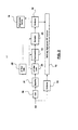
- an RF signal is received by an antenna 10.
- the antenna is connected to a simple low power receiver 17, which is constantly listening to incoming signals, and an ordinary high power receiver 15, which is normally in a sleep mode in which it is turned off or consumes minimal power.
- the antenna 10 is connected to a receiver chain consisting of a simple band pass filter 11, a down converter 12, a comparator 13, and an analyzer 14.
- the analyzer 14 is connected to a high power RF device 16 and the ordinary high power receiver 15. After filtering in the band pass filter 11, the incoming signal is down-converted by the down-converter 12 and then passed through the comparator 13, which acts as a simple decoder.
- the antenna 10 is also connected to an ordinary high power receiver 15, which is used for receiving data when in wake-up mode.
- the ordinary high power receiver 15 may or may not be used to communicate with the high power device 16.
- the simple receiver 17 can bc made totally separate, complete with its own antenna, or it can use part of the main RF communication system.
- the external RF signal to wake up the device may or may not use the same frequency as is used for normal data communication.
- the incoming RF signal picked up by the antenna is fed into the simple receiver circuit 17.
- the modulation can, for example, be Frequency Shift Keying (FSK), which is significantly lowered in frequency by the down converter. This reduction in frequency enables power saving in both the comparator 13 and the analyzer 14.
- the down-converter can reduce the frequency of an incoming signal from the MHz to KHz range.
- the analyzer 14 includes digital logic to separate out logic ones in the FSK signal.
- the timing of the frequency shifts and the embedded digital code are used to prevent the receiver 17 from turning on the ordinary high power RF receiver 15.
- the signal may be amplitude modulated using Pulse Position Modulation (PPM), Pulse Width Modulation (PWM) or Pulse Amplitude Modulation (PAM), provided a suitable analyzer 14 is used.
- PPM Pulse Position Modulation
- PWM Pulse Width Modulation
- PAM Pulse Amplitude Modulation
- the frequency band used to wake -up the device can be different from the one used for ordinary communication, thus enabling higher power levels in the wake-up signal than otherwise allowed (many frequency bands used in various data applications have an upper power limit).
- the antenna 10 receiving the RF signal is a wide band antenna enabling the frequency of the wake-up signal to be different from the ordinary frequency without using a separate antenna.
- a separate antenna can be employed.
- the signal picked up by the antenna is fed into the low power band-pass filter 11, which filters the incoming signal around the chosen wake-up frequency, e.g., 27 MHz.
- the filtered signal is then fed into the comparator 13 that after the down conversion detects an incoming signal with an amplitude higher than a preset level and outputs a digital signal to the analyzer.
- the comparator 13 thus acts as a decoder that decodes the incoming RF-signal (if any), and if the frequency is correct starts to convert the signal into logical ones '1' and zeros '0 '.
- the analyzer 14 compares the digital bit stream with a preset wake up code stored in memory, and if found correct turns on the ordinary high power RF receiver 15 or another high power device 16.
- the receiver 15 then receives the incoming signal in its wake-up mode.
- the receiver 15 and high power device 16 are programmed to return to the sleep mode after a predetermined period of inactivity.
- a tag is used in circuits that do not have a battery. Such circuits include ID cards for door opening systems.
- the tag has a pick-up coil 20 and a rectifier 21 that half wave rectifies the incoming signal and feeds it into two branches.
- One branch has a low pass filter 23 with a very long time constant ( ⁇ ) that turns the rectified signal into a DC voltage that powers the electronic circuitry of the device.
- the other branch feeds the signal into another low pass filter 22 with a much shorter time constant ( ⁇ ).
- ⁇ time constant
- Also present in the incoming RF carrier signal is communication information carrying data.
- the data can, for instance, be a simple pulse-pause scheme which is easily detected by the comparator 13 as two different voltage levels.
- the incoming RF signal can contain an address of the device for which this particular communication is intended.
- the address can be made unique for each individual device or for the same type of devices depending on the application.
- the device If the device reads the correct incoming code it turns on the full RF functionality. Otherwise it just continues to be ready to detect the correct signal.
- the tag part of the device does not consume any power and thus can be ready a 100% of the time without wasting any power. In this case the incoming frequency is lowered into the 100 Hz to 1 kHz range with blocks 21 and 23. This is desirable since otherwise can it be difficult to get enough power to supply the remainder of the circuitry.
- the coil 20 picks up the RF signal, at e.g. 70 kHz.
- the energy is then converted in the rectifier 21 and filter 22 to a DC voltage that supplies power to blocks 23, 13, 25, and 14, which together form the RF receiver.
- the low pass filter 23 filters the rectified signal and feeds it to the comparator 13, where it is converted a square wave.
- the square wave passes into the decoder 25, where the two different voltage levels are converted into ones and zeros.
- the stream of bits is then compared to a register in the analyzer 26, and if the decoded signal matches the stored code, the ordinary high power RF receiver 15 is turned on. The receiver then starts to receive the ordinary RF signal from the antenna 10.
- a correct detected code by the analyzer 26 can also turn on a separate high power block/chip 16 within the device.
- the coil 20 may be replaced by an antenna suitable for the frequency to be used.
- the proposed solution can also be used without converting the RF signal to the supply voltage for blocks 23, 13, 25 and 14.
- the described circuitry lends itself to integration in a single chip, for example, using CMOS technology.
Abstract
An electronic device with a power saving circuit incorporates a radio frequency receiver
with low power consumption and including a frequency down converter. A functional
device, which may be a high power radio receiver, is normally turned off during a period
of inactivity. An analyzer detects a predetermined identification code in a received radio
frequency signal and outputs a signal to turn on the functional device.
Description
- This invention relates to communication devices, and in particular to a method of saving power in such devices and a power saving circuit for use with such devices.
- More and more electronic devices are employing RF operating at higher and higher frequencies for communications. Similar devices exist using infrared and optical communication means. Such devices today often operate in the region of many hundreds of MHz to GHz. Such high frequencies imply high power consumption. Since the devices are generally battery powered, power saving becomes an important issue. Many current communication devices consume too much power to leave the communication function on all the time. This is especially true in the case of ultra low power RF devices used, for example, in medical applications. RF can also be used as a power switch to turn on and off a complete function within a device that may or may not use RF.
- In RF modern devices it is generally not necessary to have the RF function on at 100% level of operation constantly. Therefore the RF function often has power saving features. There are four main techniques in use today.
- The first technique is to let the user switch the device off when the device is not in use. This results in the most efficient power saving but is often not acceptable, e.g., in a mobile phone or a pacemaker.
- The second technique is to switch the RF function off for a period of time, known as the sleep mode, for example, 30 seconds, when the communication link is inactive, and then switch it on for a few seconds to decide if an RF signal is present. If so the device is restored to full functionality; if not the device goes into sleep mode again.
- In the third technique the RF receiver is not fully on; instead it only listens to determine whether an RF signal is present that might want to communicate with the device. If the receiver circuit in power down mode is made simple or operates on a much lower frequency than the normal carrier, a lot of current can be saved. If the device detects a signal while in power down mode, it returns to full functionality and starts detection to determine whether the detected signal is intended for the device.
- A fourth technique relies on a combination of the second and third techniques.
- The disadvantages with second technique are that in some cases the user expects to be serviced very rapidly. If the device is turned on too frequently to detect whether a signal is present, the advantages of power saving are largely lost.
- The disadvantage with the third technique are that if the receiver is made to have a low power consumption, it will generally be very simple and is susceptible of detecting a much wider spectrum of signals than intended. With the amount of RF signals in the air today, the low power receiver is liable to wake up the full RF functionality almost all the time. In certain environments the power saving functionality can be effectively lost.
- According to the present invention there is provided a power saving circuit for activating an electronic device with a sleep mode and a wake-up mode, comprising a radio frequency receiver with low power consumption including a down-converter for reducing the frequency of a received signal; a decoder for decoding a received radio frequency signal; and an analyzer for detecting a predetermined identification code in said received radio frequency signal and activating said electronic device in response to detection of said predetermined identification code.
- Down-conversion of the received signal significantly increases the power saving.
- The method in accordance with the invention uses a low power simplified receiver with a down conversion of the received frequency included to save power wherein an identification scheme is employed during the low energy wake-up stage. The identification code, which is unique for the particular device requested or family of devices, is present in the initial RF-transmission. The ability to detect and identify the code is already-present at the low power receiver stage. The advantage of this arrangement is twofold: First even if a very simple low power receiver is used, which detects signals all the time, the identification code associated with the wake-up signal prevents it from starting any high power RF functionality. Secondly the down conversion increases the power saving even further because the rest of the low power receiver operates on kHz signals instead of MHz.
- The method can be applied in stand-alone or other low power devices that need to be in low power mode for long periods of time and then activated and deactivated with the described RF signal. These devices may or may not employ RF themselves. For example, the electronic device can be a receiver of infrared or optical signals.
- In another aspect the invention provides a method of saving power in a remote electronic device having a sleep mode and a wake-up mode, comprising transmitting a radio frequency signal with an identification code; receiving said radio frequency signal at said remote device in the sleep mode; down-converting said received radio frequency signal; decoding said down-converted received radio frequency signal; and in response to detection of a predetermined identification code in said received radio frequency signal, switching said remote electronic device to the wake-up mode.
- The invention will now be described in more detail, by way of example only, with reference to the accompanying drawings, in which:-
- Figure 1 is a block diagram of a first embodiment of a power saving circuit; and
- Figure 2 is a block diagram of a second embodiment of a power saving circuit.
-
- In the embodiments, like parts have like reference numerals.
- In Figure 1, an RF signal is received by an
antenna 10. The antenna is connected to a simplelow power receiver 17, which is constantly listening to incoming signals, and an ordinaryhigh power receiver 15, which is normally in a sleep mode in which it is turned off or consumes minimal power. - Within the
low power receiver 17, theantenna 10 is connected to a receiver chain consisting of a simpleband pass filter 11, adown converter 12, acomparator 13, and ananalyzer 14. In the embodiment shown, theanalyzer 14 is connected to a highpower RF device 16 and the ordinaryhigh power receiver 15. After filtering in theband pass filter 11, the incoming signal is down-converted by the down-converter 12 and then passed through thecomparator 13, which acts as a simple decoder. - The
antenna 10 is also connected to an ordinaryhigh power receiver 15, which is used for receiving data when in wake-up mode. The ordinaryhigh power receiver 15 may or may not be used to communicate with thehigh power device 16. - The
simple receiver 17 can bc made totally separate, complete with its own antenna, or it can use part of the main RF communication system. The external RF signal to wake up the device may or may not use the same frequency as is used for normal data communication. - The incoming RF signal picked up by the antenna is fed into the
simple receiver circuit 17. The modulation can, for example, be Frequency Shift Keying (FSK), which is significantly lowered in frequency by the down converter. This reduction in frequency enables power saving in both thecomparator 13 and theanalyzer 14. The down-converter can reduce the frequency of an incoming signal from the MHz to KHz range. - The
analyzer 14 includes digital logic to separate out logic ones in the FSK signal. The timing of the frequency shifts and the embedded digital code are used to prevent thereceiver 17 from turning on the ordinary highpower RF receiver 15. Alternatively, the signal may be amplitude modulated using Pulse Position Modulation (PPM), Pulse Width Modulation (PWM) or Pulse Amplitude Modulation (PAM), provided asuitable analyzer 14 is used. - The frequency band used to wake -up the device can be different from the one used for ordinary communication, thus enabling higher power levels in the wake-up signal than otherwise allowed (many frequency bands used in various data applications have an upper power limit).
- It will be appreciated that modulation schemes other than the above mentioned can be employed as will be understood by one skilled in the art.
- In this exemplary embodiment, the
antenna 10 receiving the RF signal is a wide band antenna enabling the frequency of the wake-up signal to be different from the ordinary frequency without using a separate antenna. However, in an alternative embodiment, a separate antenna can be employed. - The signal picked up by the antenna is fed into the low power band-
pass filter 11, which filters the incoming signal around the chosen wake-up frequency, e.g., 27 MHz. The filtered signal is then fed into thecomparator 13 that after the down conversion detects an incoming signal with an amplitude higher than a preset level and outputs a digital signal to the analyzer. Thecomparator 13 thus acts as a decoder that decodes the incoming RF-signal (if any), and if the frequency is correct starts to convert the signal into logical ones '1' and zeros '0 '. Theanalyzer 14 then compares the digital bit stream with a preset wake up code stored in memory, and if found correct turns on the ordinary highpower RF receiver 15 or anotherhigh power device 16. Thereceiver 15 then receives the incoming signal in its wake-up mode. - The
receiver 15 andhigh power device 16 are programmed to return to the sleep mode after a predetermined period of inactivity. - To further improve the power saving function, use can be made of a so-called RF tag as shown in the embodiment illustrated in Figure 2. A tag is used in circuits that do not have a battery. Such circuits include ID cards for door opening systems. The tag has a pick-up
coil 20 and arectifier 21 that half wave rectifies the incoming signal and feeds it into two branches. One branch has alow pass filter 23 with a very long time constant (τ) that turns the rectified signal into a DC voltage that powers the electronic circuitry of the device. The other branch feeds the signal into anotherlow pass filter 22 with a much shorter time constant (τ). Also present in the incoming RF carrier signal is communication information carrying data. The data can, for instance, be a simple pulse-pause scheme which is easily detected by thecomparator 13 as two different voltage levels. Thus the incoming RF signal can contain an address of the device for which this particular communication is intended. The address can be made unique for each individual device or for the same type of devices depending on the application. - If the device reads the correct incoming code it turns on the full RF functionality. Otherwise it just continues to be ready to detect the correct signal. The tag part of the device does not consume any power and thus can be ready a 100% of the time without wasting any power. In this case the incoming frequency is lowered into the 100 Hz to 1 kHz range with
blocks - In Figure 2, the
coil 20 picks up the RF signal, at e.g. 70 kHz. The energy is then converted in therectifier 21 andfilter 22 to a DC voltage that supplies power to blocks 23, 13, 25, and 14, which together form the RF receiver. Thelow pass filter 23 filters the rectified signal and feeds it to thecomparator 13, where it is converted a square wave. The square wave passes into thedecoder 25, where the two different voltage levels are converted into ones and zeros. The stream of bits is then compared to a register in the analyzer 26, and if the decoded signal matches the stored code, the ordinary highpower RF receiver 15 is turned on. The receiver then starts to receive the ordinary RF signal from theantenna 10. - A correct detected code by the analyzer 26 can also turn on a separate high power block/
chip 16 within the device. - Alternatively the
coil 20 may be replaced by an antenna suitable for the frequency to be used. The proposed solution can also be used without converting the RF signal to the supply voltage forblocks - The described circuitry lends itself to integration in a single chip, for example, using CMOS technology.
- It will be appreciated by one skilled in the art that the above description represents an exemplary embodiment, and that many variants within the scope of the appended claims are possible without departing from the scope of the invention.
Claims (23)
- A power saving circuit for activating an electronic device with a sleep mode and a wake-up mode, comprising:a radio frequency receiver with low power consumption including:a down-converter for reducing the frequency of a received signal;a decoder for decoding a received radio frequency signal; andan analyzer for detecting a predetermined identification code in said received radio frequency signal and activating said electronic device in response to detection of said predetermined identification code.
- A power saving circuit as claimed in claim 1, wherein said electronic device is a high power radio frequency receiver for receiving a communication signal.
- A power saving circuit as claimed in claim 2, wherein said low power radio frequency receiver forms part of said high power radio frequency receiver.
- A power saving circuit as claimed in claim 2, wherein said low power radio frequency receiver is separate from said high power radio frequency receiver.
- A power saving circuit as claimed in claim 1, wherein said identification code includes an address of said electronic device.
- A power saving circuit as claimed in claim 2, wherein said low power receiver operates at a different frequency from said high power radio frequency receiver.
- A power saving circuit as claimed in claim 1, wherein said identification code is modulated using frequency shift keying.
- A power saving circuit as claimed in claim 1, wherein said identification code is modulated using amplitude shift keying.
- A power saving circuit as claimed in claim 1, wherein said receiver with low power consumption further includes a band pass filter and a comparator acting as said decoder.
- A power saving circuit as claimed in claim 1, further comprising a sensor and a converter for producing DC power from said received radio frequency signal to power said radio frequency receiver with low power consumption.
- A power saving circuit as claimed in claim 10, wherein said sensor comprises a pick-up coil.
- A power saving circuit as claimed in claim 11, further comprising a rectifier for rectifying said received signal and feeding it to a low pass filter having a long time constant for generating a DC voltage therefrom and to a low pass filter having a shorter time constant to down-convert said received signal.
- A power saving circuit as in claim 2, where said electronic device is a receiver of infrared or optical signals.
- A method of saving power in a remote electronic device having a sleep mode and a wake-up mode, comprising:transmitting a radio frequency signal with an identification code;receiving said radio frequency signal at said remote device in the sleep mode;down-converting said received radio frequency signal;decoding said down-converted received radio frequency signal; andin response to detection of a predetermined identification code in said received radio frequency signal, switching said remote electronic device to the wake-up mode.
- A method as claimed in claim 14, wherein said electronic device includes a high power radio frequency receiver that is activated in response to detection of said predetermined identification code.
- A method as claimed in claim 14, wherein said identification code includes an address of said device.
- A method as claimed in claim 15, wherein said signal is transmitted at a frequency different from a frequency of operation of said high power receiver.
- A method as claimed in claim 14, wherein said identification code is modulated using frequency shift keying.
- A method as claimed in claim 14, wherein said identification code is modulated using amplitude shift keying.
- A method as claimed in claim 14, wherein power for receiving said signal in said sleep mode is derived from said received radio frequency signal.
- A method as claimed in claim 20, wherein said received radio frequency signal is rectified to produce said power.
- A method as claimed in claim 15, wherein said signal is received in a low power receiver separate from said high power receiver.
- A method as claimed in claim 15, wherein said signal is received in a low power receiver forming part of said high power receiver.
Applications Claiming Priority (2)
| Application Number | Priority Date | Filing Date | Title |
|---|---|---|---|
| GB2084499 | 2002-04-10 | ||
| GBGB0208449.9A GB0208449D0 (en) | 2002-04-10 | 2002-04-10 | Method of saving power in RF devices |
Publications (1)
| Publication Number | Publication Date |
|---|---|
| EP1353447A1 true EP1353447A1 (en) | 2003-10-15 |
Family
ID=9934727
Family Applications (1)
| Application Number | Title | Priority Date | Filing Date |
|---|---|---|---|
| EP03100918A Withdrawn EP1353447A1 (en) | 2002-04-10 | 2003-04-07 | Method of saving power in communication devices |
Country Status (3)
| Country | Link |
|---|---|
| US (1) | US20030236077A1 (en) |
| EP (1) | EP1353447A1 (en) |
| GB (1) | GB0208449D0 (en) |
Cited By (4)
| Publication number | Priority date | Publication date | Assignee | Title |
|---|---|---|---|---|
| WO2006000976A1 (en) * | 2004-06-24 | 2006-01-05 | Koninklijke Philips Electronics N.V. | Zero power radio |
| EP1734671A2 (en) | 2005-06-13 | 2006-12-20 | Gilat Satellite Networks Ltd. | Switching VSAT transmitter with smart stand-by mode |
| EP1772977A2 (en) * | 2005-10-06 | 2007-04-11 | Broadcom Corporation | Mobile communication device with low power signal detector |
| EP1892011A2 (en) | 2006-08-22 | 2008-02-27 | BIOTRONIK CRM Patent AG | Electromedical implant |
Families Citing this family (31)
| Publication number | Priority date | Publication date | Assignee | Title |
|---|---|---|---|---|
| US7574168B2 (en) * | 2005-06-16 | 2009-08-11 | Terahop Networks, Inc. | Selective GPS denial system |
| US7583769B2 (en) * | 2005-06-16 | 2009-09-01 | Terahop Netowrks, Inc. | Operating GPS receivers in GPS-adverse environment |
| US8315563B2 (en) | 2000-12-22 | 2012-11-20 | Google Inc. | Wireless reader tags (WRTs) with sensor components in asset monitoring and tracking systems |
| US7522568B2 (en) | 2000-12-22 | 2009-04-21 | Terahop Networks, Inc. | Propagating ad hoc wireless networks based on common designation and routine |
| US20080303897A1 (en) | 2000-12-22 | 2008-12-11 | Terahop Networks, Inc. | Visually capturing and monitoring contents and events of cargo container |
| US7940716B2 (en) | 2005-07-01 | 2011-05-10 | Terahop Networks, Inc. | Maintaining information facilitating deterministic network routing |
| US7783246B2 (en) | 2005-06-16 | 2010-08-24 | Terahop Networks, Inc. | Tactical GPS denial and denial detection system |
| US7742773B2 (en) | 2005-10-31 | 2010-06-22 | Terahop Networks, Inc. | Using GPS and ranging to determine relative elevation of an asset |
| US20060194564A1 (en) * | 2003-07-30 | 2006-08-31 | Takehiro Hokimoto | Radio transmitting/receiving apparatus and intermittent transmission/reception control method of radio transmitting/receiving apparatus |
| US7142107B2 (en) | 2004-05-27 | 2006-11-28 | Lawrence Kates | Wireless sensor unit |
| US7295828B2 (en) * | 2004-06-01 | 2007-11-13 | Ati Technologies Inc. | Differential signal comparator |
| US8897884B2 (en) * | 2004-11-26 | 2014-11-25 | St. Jude Medical Ab | Implantable medical device with a voltage protection circuit |
| WO2007100343A1 (en) * | 2005-06-03 | 2007-09-07 | Terahop Networks Inc. | Remote sensor interface (rsi) stepped wake-up sequence |
| CN1913354B (en) * | 2005-08-12 | 2010-05-26 | 鸿富锦精密工业(深圳)有限公司 | System and method for recovering power supply to electronic device |
| US20090129306A1 (en) | 2007-02-21 | 2009-05-21 | Terahop Networks, Inc. | Wake-up broadcast including network information in common designation ad hoc wireless networking |
| WO2008036425A1 (en) * | 2006-01-01 | 2008-03-27 | Terahop Networks, Inc. | Determining presence of radio frequency communication device |
| US8223680B2 (en) | 2007-02-21 | 2012-07-17 | Google Inc. | Mesh network control using common designation wake-up |
| US8056988B2 (en) * | 2008-01-15 | 2011-11-15 | Hui-Lan Pan | Cabinet assembly |
| US8023928B2 (en) | 2008-01-16 | 2011-09-20 | Intuitive Research And Technology | System and method for monitoring an analog data signal |
| US8233877B2 (en) * | 2008-04-09 | 2012-07-31 | Telefonaktiebolaget Lm Ericsson (Publ) | Discontinuous reception of bursts for voice calls |
| WO2009140669A2 (en) | 2008-05-16 | 2009-11-19 | Terahop Networks, Inc. | Securing, monitoring and tracking shipping containers |
| US8462662B2 (en) | 2008-05-16 | 2013-06-11 | Google Inc. | Updating node presence based on communication pathway |
| US8681218B1 (en) * | 2008-07-03 | 2014-03-25 | Rockwell Collins, Inc. | System for providing spatial awareness of transmissions of energy in an environment |
| US8391435B2 (en) | 2008-12-25 | 2013-03-05 | Google Inc. | Receiver state estimation in a duty cycled radio |
| US8300551B2 (en) | 2009-01-28 | 2012-10-30 | Google Inc. | Ascertaining presence in wireless networks |
| US8705523B2 (en) | 2009-02-05 | 2014-04-22 | Google Inc. | Conjoined class-based networking |
| US9325543B2 (en) * | 2012-11-11 | 2016-04-26 | Ethertronics, Inc. | Multi-mode active circuit control and activation system |
| US9204394B2 (en) * | 2013-03-12 | 2015-12-01 | Qualcomm Incorporated | Signature-coded wake-up transmission |
| US9112790B2 (en) | 2013-06-25 | 2015-08-18 | Google Inc. | Fabric network |
| US9510288B1 (en) * | 2015-08-06 | 2016-11-29 | Texas Instruments Incorporated | Concurrent, reconfigurable, low power harmonic wake-up and main radio receiver |
| US20180202224A1 (en) * | 2017-01-17 | 2018-07-19 | Crestron Electronics, Inc. | Battery operated roller shade |
Citations (5)
| Publication number | Priority date | Publication date | Assignee | Title |
|---|---|---|---|---|
| JPH0264494A (en) * | 1988-08-31 | 1990-03-05 | Yamatake Honeywell Co Ltd | Radio receiving apparatus |
| EP0358166A2 (en) * | 1988-09-07 | 1990-03-14 | Sanyo Electric Co., Ltd. | Power saving arrangement and power saving method |
| EP0792030A2 (en) * | 1992-06-29 | 1997-08-27 | Motorola, Inc. | Dual mode receiver having battery saving capability |
| US5940447A (en) * | 1996-08-30 | 1999-08-17 | Motorola, Inc. | Wireless powered communication device using power signal sampling and method |
| US6329808B1 (en) * | 1998-06-18 | 2001-12-11 | Stmicroelectronics S.A. | Method and system for the detection, by inductive coupling, of a load modulation signal |
Family Cites Families (3)
| Publication number | Priority date | Publication date | Assignee | Title |
|---|---|---|---|---|
| US5790946A (en) * | 1993-07-15 | 1998-08-04 | Rotzoll; Robert R. | Wake up device for a communications system |
| US6100814A (en) * | 1996-05-07 | 2000-08-08 | Lear Automotive Dearborn, Inc. | Remote control wake up detector system |
| GB9723743D0 (en) * | 1997-11-12 | 1998-01-07 | Philips Electronics Nv | Battery economising in a communications system |
-
2002
- 2002-04-10 GB GBGB0208449.9A patent/GB0208449D0/en not_active Ceased
-
2003
- 2003-04-07 US US10/408,274 patent/US20030236077A1/en not_active Abandoned
- 2003-04-07 EP EP03100918A patent/EP1353447A1/en not_active Withdrawn
Patent Citations (5)
| Publication number | Priority date | Publication date | Assignee | Title |
|---|---|---|---|---|
| JPH0264494A (en) * | 1988-08-31 | 1990-03-05 | Yamatake Honeywell Co Ltd | Radio receiving apparatus |
| EP0358166A2 (en) * | 1988-09-07 | 1990-03-14 | Sanyo Electric Co., Ltd. | Power saving arrangement and power saving method |
| EP0792030A2 (en) * | 1992-06-29 | 1997-08-27 | Motorola, Inc. | Dual mode receiver having battery saving capability |
| US5940447A (en) * | 1996-08-30 | 1999-08-17 | Motorola, Inc. | Wireless powered communication device using power signal sampling and method |
| US6329808B1 (en) * | 1998-06-18 | 2001-12-11 | Stmicroelectronics S.A. | Method and system for the detection, by inductive coupling, of a load modulation signal |
Non-Patent Citations (1)
| Title |
|---|
| PATENT ABSTRACTS OF JAPAN vol. 014, no. 245 (P - 1052) 24 May 1990 (1990-05-24) * |
Cited By (12)
| Publication number | Priority date | Publication date | Assignee | Title |
|---|---|---|---|---|
| US9112579B2 (en) | 1998-11-03 | 2015-08-18 | Gilat Satellite Networks Ltd. | Switching VSAT transmitter with smart stand-by mode |
| WO2006000976A1 (en) * | 2004-06-24 | 2006-01-05 | Koninklijke Philips Electronics N.V. | Zero power radio |
| CN101019334B (en) * | 2004-06-24 | 2011-07-06 | Nxp股份有限公司 | Zero power radio |
| EP1734671A2 (en) | 2005-06-13 | 2006-12-20 | Gilat Satellite Networks Ltd. | Switching VSAT transmitter with smart stand-by mode |
| EP1734671A3 (en) * | 2005-06-13 | 2009-01-21 | Gilat Satellite Networks Ltd. | Switching VSAT transmitter with smart stand-by mode |
| EP1772977A2 (en) * | 2005-10-06 | 2007-04-11 | Broadcom Corporation | Mobile communication device with low power signal detector |
| EP1772977A3 (en) * | 2005-10-06 | 2010-11-24 | Broadcom Corporation | Mobile communication device with low power signal detector |
| US8532718B2 (en) | 2005-10-06 | 2013-09-10 | Broadcom Corporation | Mobile communication device with low power signal detector |
| US8892177B2 (en) | 2005-10-06 | 2014-11-18 | Broadcom Corporation | Mobile communication device with low power signal detector |
| EP1892011A2 (en) | 2006-08-22 | 2008-02-27 | BIOTRONIK CRM Patent AG | Electromedical implant |
| EP1892011A3 (en) * | 2006-08-22 | 2009-08-05 | BIOTRONIK CRM Patent AG | Electromedical implant |
| US7948362B2 (en) | 2006-08-22 | 2011-05-24 | Biotronik Crm Patent Ag | Implantable medical transceiver device |
Also Published As
| Publication number | Publication date |
|---|---|
| GB0208449D0 (en) | 2002-05-22 |
| US20030236077A1 (en) | 2003-12-25 |
Similar Documents
| Publication | Publication Date | Title |
|---|---|---|
| EP1353447A1 (en) | Method of saving power in communication devices | |
| US6920342B2 (en) | Electronic device having an operating mode and an energy saving standby mode, and a method for switching between the two modes | |
| US8538544B2 (en) | Implantable RF telemetry devices with power saving mode | |
| CN102017435B (en) | Wake-up receiver and wake-up method using duty cycling and power off technique | |
| US7019617B2 (en) | Radio frequency identification devices, backscatter communication device wake-up methods, communication device wake-up methods and a radio frequency identification device wake-up method | |
| US7912443B2 (en) | Wake up device for communications system and methods | |
| KR100883218B1 (en) | Noise alarm timer function for three-axis low frequency transponder | |
| US8164416B2 (en) | Programmable selective wake-up for radio frequency transponder | |
| KR100691175B1 (en) | Wireless transceiver | |
| US20050237160A1 (en) | Reducing false wake-up in a low frequency transponder | |
| WO2015042362A1 (en) | Wake-up receiver with automatic interference rejection | |
| US7587195B2 (en) | Wireless communications apparatus made operative in dependent upon a received signal strength | |
| EP3047619B1 (en) | Wake-up receiver with automatic interference rejection | |
| US20090156245A1 (en) | Wireless Communication Unit, Power Control Method for Wireless Communication Unit and Wireless Network | |
| CN101583203A (en) | Remote control device and remote control method for mobile phone | |
| JP2611670B2 (en) | Selective call receiver | |
| JP2007028628A (en) | Ultra-low power high-efficiency wireless digital receiver | |
| US6831953B2 (en) | Method of, and a radio terminal for, detecting the presence of a 2-FSK signal | |
| JPH09298486A (en) | Contactless data transmission reception method and its equipment | |
| Köble et al. | A narrow-band and ultra-low-power 433 MHz wake-up receiver | |
| US6750770B2 (en) | Transponder with a changeable circuit configuration | |
| KR20070112491A (en) | Rfid tag with real-time wake-up function utilizing communication signal with periodic structure | |
| US6885256B2 (en) | Input circuit for an HF-transmitting component | |
| JP2007281768A (en) | Rf device, and rf data transmission method | |
| WO2011121663A1 (en) | Receiver device and remote control system |
Legal Events
| Date | Code | Title | Description |
|---|---|---|---|
| PUAI | Public reference made under article 153(3) epc to a published international application that has entered the european phase |
Free format text: ORIGINAL CODE: 0009012 |
|
| AK | Designated contracting states |
Kind code of ref document: A1 Designated state(s): AT BE BG CH CY CZ DE DK EE ES FI FR GB GR HU IE IT LI LU MC NL PT SE SI SK TR |
|
| AX | Request for extension of the european patent |
Extension state: AL LT LV MK |
|
| STAA | Information on the status of an ep patent application or granted ep patent |
Free format text: STATUS: THE APPLICATION HAS BEEN WITHDRAWN |
|
| 17P | Request for examination filed |
Effective date: 20031118 |
|
| 18W | Application withdrawn |
Effective date: 20031215 |