EP1362339B1 - Low-power organic light emitting diode pixel circuit - Google Patents
Low-power organic light emitting diode pixel circuit Download PDFInfo
- Publication number
- EP1362339B1 EP1362339B1 EP01272506A EP01272506A EP1362339B1 EP 1362339 B1 EP1362339 B1 EP 1362339B1 EP 01272506 A EP01272506 A EP 01272506A EP 01272506 A EP01272506 A EP 01272506A EP 1362339 B1 EP1362339 B1 EP 1362339B1
- Authority
- EP
- European Patent Office
- Prior art keywords
- oled
- circuit
- pixel
- data
- display
- Prior art date
- Legal status (The legal status is an assumption and is not a legal conclusion. Google has not performed a legal analysis and makes no representation as to the accuracy of the status listed.)
- Expired - Lifetime
Links
- 230000003068 static effect Effects 0.000 claims abstract description 13
- 239000004065 semiconductor Substances 0.000 claims abstract description 9
- 229910044991 metal oxide Inorganic materials 0.000 claims abstract description 7
- 150000004706 metal oxides Chemical class 0.000 claims abstract description 7
- 230000002441 reversible effect Effects 0.000 claims description 16
- 230000005669 field effect Effects 0.000 abstract description 2
- 239000010410 layer Substances 0.000 description 11
- 238000010586 diagram Methods 0.000 description 7
- 238000005516 engineering process Methods 0.000 description 7
- 229910052710 silicon Inorganic materials 0.000 description 7
- 239000010703 silicon Substances 0.000 description 7
- 239000000758 substrate Substances 0.000 description 7
- XUIMIQQOPSSXEZ-UHFFFAOYSA-N Silicon Chemical compound [Si] XUIMIQQOPSSXEZ-UHFFFAOYSA-N 0.000 description 6
- 239000004020 conductor Substances 0.000 description 6
- 230000002829 reductive effect Effects 0.000 description 6
- 230000006870 function Effects 0.000 description 5
- 239000011159 matrix material Substances 0.000 description 5
- 238000012360 testing method Methods 0.000 description 5
- 230000000694 effects Effects 0.000 description 4
- 239000011368 organic material Substances 0.000 description 4
- 239000003990 capacitor Substances 0.000 description 3
- 229910021419 crystalline silicon Inorganic materials 0.000 description 3
- 238000000034 method Methods 0.000 description 3
- 239000012044 organic layer Substances 0.000 description 3
- 230000003071 parasitic effect Effects 0.000 description 3
- 239000010409 thin film Substances 0.000 description 3
- 229920001621 AMOLED Polymers 0.000 description 2
- 230000015556 catabolic process Effects 0.000 description 2
- 238000009792 diffusion process Methods 0.000 description 2
- 238000009826 distribution Methods 0.000 description 2
- 238000005286 illumination Methods 0.000 description 2
- 230000001788 irregular Effects 0.000 description 2
- 230000000670 limiting effect Effects 0.000 description 2
- 238000004519 manufacturing process Methods 0.000 description 2
- 230000000737 periodic effect Effects 0.000 description 2
- 229910021420 polycrystalline silicon Inorganic materials 0.000 description 2
- 229920005591 polysilicon Polymers 0.000 description 2
- 238000003860 storage Methods 0.000 description 2
- 238000010521 absorption reaction Methods 0.000 description 1
- 229910021417 amorphous silicon Inorganic materials 0.000 description 1
- 238000003491 array Methods 0.000 description 1
- 239000000919 ceramic Substances 0.000 description 1
- 230000000295 complement effect Effects 0.000 description 1
- 239000006059 cover glass Substances 0.000 description 1
- 238000013500 data storage Methods 0.000 description 1
- 230000007547 defect Effects 0.000 description 1
- 230000008021 deposition Effects 0.000 description 1
- 230000006866 deterioration Effects 0.000 description 1
- 238000007599 discharging Methods 0.000 description 1
- 230000007613 environmental effect Effects 0.000 description 1
- 238000007667 floating Methods 0.000 description 1
- 239000011521 glass Substances 0.000 description 1
- AMGQUBHHOARCQH-UHFFFAOYSA-N indium;oxotin Chemical compound [In].[Sn]=O AMGQUBHHOARCQH-UHFFFAOYSA-N 0.000 description 1
- 238000012423 maintenance Methods 0.000 description 1
- 239000000463 material Substances 0.000 description 1
- 229910052751 metal Inorganic materials 0.000 description 1
- 239000002184 metal Substances 0.000 description 1
- 229910021424 microcrystalline silicon Inorganic materials 0.000 description 1
- TWNQGVIAIRXVLR-UHFFFAOYSA-N oxo(oxoalumanyloxy)alumane Chemical compound O=[Al]O[Al]=O TWNQGVIAIRXVLR-UHFFFAOYSA-N 0.000 description 1
- 239000004033 plastic Substances 0.000 description 1
- 229920000642 polymer Polymers 0.000 description 1
- 230000001681 protective effect Effects 0.000 description 1
- 238000007789 sealing Methods 0.000 description 1
- 238000000926 separation method Methods 0.000 description 1
Images


Classifications
-
- G—PHYSICS
- G09—EDUCATION; CRYPTOGRAPHY; DISPLAY; ADVERTISING; SEALS
- G09G—ARRANGEMENTS OR CIRCUITS FOR CONTROL OF INDICATING DEVICES USING STATIC MEANS TO PRESENT VARIABLE INFORMATION
- G09G3/00—Control arrangements or circuits, of interest only in connection with visual indicators other than cathode-ray tubes
- G09G3/20—Control arrangements or circuits, of interest only in connection with visual indicators other than cathode-ray tubes for presentation of an assembly of a number of characters, e.g. a page, by composing the assembly by combination of individual elements arranged in a matrix no fixed position being assigned to or needed to be assigned to the individual characters or partial characters
- G09G3/22—Control arrangements or circuits, of interest only in connection with visual indicators other than cathode-ray tubes for presentation of an assembly of a number of characters, e.g. a page, by composing the assembly by combination of individual elements arranged in a matrix no fixed position being assigned to or needed to be assigned to the individual characters or partial characters using controlled light sources
- G09G3/30—Control arrangements or circuits, of interest only in connection with visual indicators other than cathode-ray tubes for presentation of an assembly of a number of characters, e.g. a page, by composing the assembly by combination of individual elements arranged in a matrix no fixed position being assigned to or needed to be assigned to the individual characters or partial characters using controlled light sources using electroluminescent panels
- G09G3/32—Control arrangements or circuits, of interest only in connection with visual indicators other than cathode-ray tubes for presentation of an assembly of a number of characters, e.g. a page, by composing the assembly by combination of individual elements arranged in a matrix no fixed position being assigned to or needed to be assigned to the individual characters or partial characters using controlled light sources using electroluminescent panels semiconductive, e.g. using light-emitting diodes [LED]
- G09G3/3208—Control arrangements or circuits, of interest only in connection with visual indicators other than cathode-ray tubes for presentation of an assembly of a number of characters, e.g. a page, by composing the assembly by combination of individual elements arranged in a matrix no fixed position being assigned to or needed to be assigned to the individual characters or partial characters using controlled light sources using electroluminescent panels semiconductive, e.g. using light-emitting diodes [LED] organic, e.g. using organic light-emitting diodes [OLED]
- G09G3/3225—Control arrangements or circuits, of interest only in connection with visual indicators other than cathode-ray tubes for presentation of an assembly of a number of characters, e.g. a page, by composing the assembly by combination of individual elements arranged in a matrix no fixed position being assigned to or needed to be assigned to the individual characters or partial characters using controlled light sources using electroluminescent panels semiconductive, e.g. using light-emitting diodes [LED] organic, e.g. using organic light-emitting diodes [OLED] using an active matrix
- G09G3/3233—Control arrangements or circuits, of interest only in connection with visual indicators other than cathode-ray tubes for presentation of an assembly of a number of characters, e.g. a page, by composing the assembly by combination of individual elements arranged in a matrix no fixed position being assigned to or needed to be assigned to the individual characters or partial characters using controlled light sources using electroluminescent panels semiconductive, e.g. using light-emitting diodes [LED] organic, e.g. using organic light-emitting diodes [OLED] using an active matrix with pixel circuitry controlling the current through the light-emitting element
-
- G—PHYSICS
- G09—EDUCATION; CRYPTOGRAPHY; DISPLAY; ADVERTISING; SEALS
- G09G—ARRANGEMENTS OR CIRCUITS FOR CONTROL OF INDICATING DEVICES USING STATIC MEANS TO PRESENT VARIABLE INFORMATION
- G09G3/00—Control arrangements or circuits, of interest only in connection with visual indicators other than cathode-ray tubes
- G09G3/20—Control arrangements or circuits, of interest only in connection with visual indicators other than cathode-ray tubes for presentation of an assembly of a number of characters, e.g. a page, by composing the assembly by combination of individual elements arranged in a matrix no fixed position being assigned to or needed to be assigned to the individual characters or partial characters
- G09G3/22—Control arrangements or circuits, of interest only in connection with visual indicators other than cathode-ray tubes for presentation of an assembly of a number of characters, e.g. a page, by composing the assembly by combination of individual elements arranged in a matrix no fixed position being assigned to or needed to be assigned to the individual characters or partial characters using controlled light sources
- G09G3/30—Control arrangements or circuits, of interest only in connection with visual indicators other than cathode-ray tubes for presentation of an assembly of a number of characters, e.g. a page, by composing the assembly by combination of individual elements arranged in a matrix no fixed position being assigned to or needed to be assigned to the individual characters or partial characters using controlled light sources using electroluminescent panels
-
- G—PHYSICS
- G09—EDUCATION; CRYPTOGRAPHY; DISPLAY; ADVERTISING; SEALS
- G09G—ARRANGEMENTS OR CIRCUITS FOR CONTROL OF INDICATING DEVICES USING STATIC MEANS TO PRESENT VARIABLE INFORMATION
- G09G3/00—Control arrangements or circuits, of interest only in connection with visual indicators other than cathode-ray tubes
- G09G3/20—Control arrangements or circuits, of interest only in connection with visual indicators other than cathode-ray tubes for presentation of an assembly of a number of characters, e.g. a page, by composing the assembly by combination of individual elements arranged in a matrix no fixed position being assigned to or needed to be assigned to the individual characters or partial characters
- G09G3/2007—Display of intermediate tones
- G09G3/2014—Display of intermediate tones by modulation of the duration of a single pulse during which the logic level remains constant
-
- G—PHYSICS
- G11—INFORMATION STORAGE
- G11C—STATIC STORES
- G11C11/00—Digital stores characterised by the use of particular electric or magnetic storage elements; Storage elements therefor
- G11C11/21—Digital stores characterised by the use of particular electric or magnetic storage elements; Storage elements therefor using electric elements
- G11C11/34—Digital stores characterised by the use of particular electric or magnetic storage elements; Storage elements therefor using electric elements using semiconductor devices
- G11C11/40—Digital stores characterised by the use of particular electric or magnetic storage elements; Storage elements therefor using electric elements using semiconductor devices using transistors
- G11C11/41—Digital stores characterised by the use of particular electric or magnetic storage elements; Storage elements therefor using electric elements using semiconductor devices using transistors forming static cells with positive feedback, i.e. cells not needing refreshing or charge regeneration, e.g. bistable multivibrator or Schmitt trigger
- G11C11/413—Auxiliary circuits, e.g. for addressing, decoding, driving, writing, sensing, timing or power reduction
- G11C11/417—Auxiliary circuits, e.g. for addressing, decoding, driving, writing, sensing, timing or power reduction for memory cells of the field-effect type
- G11C11/419—Read-write [R-W] circuits
-
- G—PHYSICS
- G09—EDUCATION; CRYPTOGRAPHY; DISPLAY; ADVERTISING; SEALS
- G09G—ARRANGEMENTS OR CIRCUITS FOR CONTROL OF INDICATING DEVICES USING STATIC MEANS TO PRESENT VARIABLE INFORMATION
- G09G2300/00—Aspects of the constitution of display devices
- G09G2300/08—Active matrix structure, i.e. with use of active elements, inclusive of non-linear two terminal elements, in the pixels together with light emitting or modulating elements
- G09G2300/0809—Several active elements per pixel in active matrix panels
- G09G2300/0842—Several active elements per pixel in active matrix panels forming a memory circuit, e.g. a dynamic memory with one capacitor
- G09G2300/0857—Static memory circuit, e.g. flip-flop
-
- G—PHYSICS
- G09—EDUCATION; CRYPTOGRAPHY; DISPLAY; ADVERTISING; SEALS
- G09G—ARRANGEMENTS OR CIRCUITS FOR CONTROL OF INDICATING DEVICES USING STATIC MEANS TO PRESENT VARIABLE INFORMATION
- G09G2300/00—Aspects of the constitution of display devices
- G09G2300/08—Active matrix structure, i.e. with use of active elements, inclusive of non-linear two terminal elements, in the pixels together with light emitting or modulating elements
- G09G2300/0809—Several active elements per pixel in active matrix panels
- G09G2300/0842—Several active elements per pixel in active matrix panels forming a memory circuit, e.g. a dynamic memory with one capacitor
- G09G2300/0861—Several active elements per pixel in active matrix panels forming a memory circuit, e.g. a dynamic memory with one capacitor with additional control of the display period without amending the charge stored in a pixel memory, e.g. by means of additional select electrodes
-
- G—PHYSICS
- G09—EDUCATION; CRYPTOGRAPHY; DISPLAY; ADVERTISING; SEALS
- G09G—ARRANGEMENTS OR CIRCUITS FOR CONTROL OF INDICATING DEVICES USING STATIC MEANS TO PRESENT VARIABLE INFORMATION
- G09G2310/00—Command of the display device
- G09G2310/02—Addressing, scanning or driving the display screen or processing steps related thereto
- G09G2310/0243—Details of the generation of driving signals
- G09G2310/0254—Control of polarity reversal in general, other than for liquid crystal displays
- G09G2310/0256—Control of polarity reversal in general, other than for liquid crystal displays with the purpose of reversing the voltage across a light emitting or modulating element within a pixel
-
- G—PHYSICS
- G09—EDUCATION; CRYPTOGRAPHY; DISPLAY; ADVERTISING; SEALS
- G09G—ARRANGEMENTS OR CIRCUITS FOR CONTROL OF INDICATING DEVICES USING STATIC MEANS TO PRESENT VARIABLE INFORMATION
- G09G2310/00—Command of the display device
- G09G2310/06—Details of flat display driving waveforms
- G09G2310/061—Details of flat display driving waveforms for resetting or blanking
- G09G2310/063—Waveforms for resetting the whole screen at once
-
- G—PHYSICS
- G09—EDUCATION; CRYPTOGRAPHY; DISPLAY; ADVERTISING; SEALS
- G09G—ARRANGEMENTS OR CIRCUITS FOR CONTROL OF INDICATING DEVICES USING STATIC MEANS TO PRESENT VARIABLE INFORMATION
- G09G2320/00—Control of display operating conditions
- G09G2320/02—Improving the quality of display appearance
- G09G2320/0233—Improving the luminance or brightness uniformity across the screen
-
- G—PHYSICS
- G09—EDUCATION; CRYPTOGRAPHY; DISPLAY; ADVERTISING; SEALS
- G09G—ARRANGEMENTS OR CIRCUITS FOR CONTROL OF INDICATING DEVICES USING STATIC MEANS TO PRESENT VARIABLE INFORMATION
- G09G2320/00—Control of display operating conditions
- G09G2320/04—Maintaining the quality of display appearance
- G09G2320/043—Preventing or counteracting the effects of ageing
- G09G2320/046—Dealing with screen burn-in prevention or compensation of the effects thereof
-
- G—PHYSICS
- G09—EDUCATION; CRYPTOGRAPHY; DISPLAY; ADVERTISING; SEALS
- G09G—ARRANGEMENTS OR CIRCUITS FOR CONTROL OF INDICATING DEVICES USING STATIC MEANS TO PRESENT VARIABLE INFORMATION
- G09G2320/00—Control of display operating conditions
- G09G2320/06—Adjustment of display parameters
- G09G2320/0626—Adjustment of display parameters for control of overall brightness
- G09G2320/0633—Adjustment of display parameters for control of overall brightness by amplitude modulation of the brightness of the illumination source
-
- G—PHYSICS
- G09—EDUCATION; CRYPTOGRAPHY; DISPLAY; ADVERTISING; SEALS
- G09G—ARRANGEMENTS OR CIRCUITS FOR CONTROL OF INDICATING DEVICES USING STATIC MEANS TO PRESENT VARIABLE INFORMATION
- G09G2320/00—Control of display operating conditions
- G09G2320/06—Adjustment of display parameters
- G09G2320/0626—Adjustment of display parameters for control of overall brightness
- G09G2320/064—Adjustment of display parameters for control of overall brightness by time modulation of the brightness of the illumination source
-
- G—PHYSICS
- G09—EDUCATION; CRYPTOGRAPHY; DISPLAY; ADVERTISING; SEALS
- G09G—ARRANGEMENTS OR CIRCUITS FOR CONTROL OF INDICATING DEVICES USING STATIC MEANS TO PRESENT VARIABLE INFORMATION
- G09G2330/00—Aspects of power supply; Aspects of display protection and defect management
- G09G2330/02—Details of power systems and of start or stop of display operation
- G09G2330/021—Power management, e.g. power saving
- G09G2330/022—Power management, e.g. power saving in absence of operation, e.g. no data being entered during a predetermined time
-
- G—PHYSICS
- G09—EDUCATION; CRYPTOGRAPHY; DISPLAY; ADVERTISING; SEALS
- G09G—ARRANGEMENTS OR CIRCUITS FOR CONTROL OF INDICATING DEVICES USING STATIC MEANS TO PRESENT VARIABLE INFORMATION
- G09G2330/00—Aspects of power supply; Aspects of display protection and defect management
- G09G2330/04—Display protection
-
- G—PHYSICS
- G09—EDUCATION; CRYPTOGRAPHY; DISPLAY; ADVERTISING; SEALS
- G09G—ARRANGEMENTS OR CIRCUITS FOR CONTROL OF INDICATING DEVICES USING STATIC MEANS TO PRESENT VARIABLE INFORMATION
- G09G3/00—Control arrangements or circuits, of interest only in connection with visual indicators other than cathode-ray tubes
- G09G3/006—Electronic inspection or testing of displays and display drivers, e.g. of LED or LCD displays
-
- G—PHYSICS
- G09—EDUCATION; CRYPTOGRAPHY; DISPLAY; ADVERTISING; SEALS
- G09G—ARRANGEMENTS OR CIRCUITS FOR CONTROL OF INDICATING DEVICES USING STATIC MEANS TO PRESENT VARIABLE INFORMATION
- G09G3/00—Control arrangements or circuits, of interest only in connection with visual indicators other than cathode-ray tubes
- G09G3/20—Control arrangements or circuits, of interest only in connection with visual indicators other than cathode-ray tubes for presentation of an assembly of a number of characters, e.g. a page, by composing the assembly by combination of individual elements arranged in a matrix no fixed position being assigned to or needed to be assigned to the individual characters or partial characters
- G09G3/22—Control arrangements or circuits, of interest only in connection with visual indicators other than cathode-ray tubes for presentation of an assembly of a number of characters, e.g. a page, by composing the assembly by combination of individual elements arranged in a matrix no fixed position being assigned to or needed to be assigned to the individual characters or partial characters using controlled light sources
- G09G3/30—Control arrangements or circuits, of interest only in connection with visual indicators other than cathode-ray tubes for presentation of an assembly of a number of characters, e.g. a page, by composing the assembly by combination of individual elements arranged in a matrix no fixed position being assigned to or needed to be assigned to the individual characters or partial characters using controlled light sources using electroluminescent panels
- G09G3/32—Control arrangements or circuits, of interest only in connection with visual indicators other than cathode-ray tubes for presentation of an assembly of a number of characters, e.g. a page, by composing the assembly by combination of individual elements arranged in a matrix no fixed position being assigned to or needed to be assigned to the individual characters or partial characters using controlled light sources using electroluminescent panels semiconductive, e.g. using light-emitting diodes [LED]
- G09G3/3208—Control arrangements or circuits, of interest only in connection with visual indicators other than cathode-ray tubes for presentation of an assembly of a number of characters, e.g. a page, by composing the assembly by combination of individual elements arranged in a matrix no fixed position being assigned to or needed to be assigned to the individual characters or partial characters using controlled light sources using electroluminescent panels semiconductive, e.g. using light-emitting diodes [LED] organic, e.g. using organic light-emitting diodes [OLED]
- G09G3/3275—Details of drivers for data electrodes
- G09G3/3291—Details of drivers for data electrodes in which the data driver supplies a variable data voltage for setting the current through, or the voltage across, the light-emitting elements
-
- H—ELECTRICITY
- H10—SEMICONDUCTOR DEVICES; ELECTRIC SOLID-STATE DEVICES NOT OTHERWISE PROVIDED FOR
- H10K—ORGANIC ELECTRIC SOLID-STATE DEVICES
- H10K59/00—Integrated devices, or assemblies of multiple devices, comprising at least one organic light-emitting element covered by group H10K50/00
-
- H—ELECTRICITY
- H10—SEMICONDUCTOR DEVICES; ELECTRIC SOLID-STATE DEVICES NOT OTHERWISE PROVIDED FOR
- H10K—ORGANIC ELECTRIC SOLID-STATE DEVICES
- H10K59/00—Integrated devices, or assemblies of multiple devices, comprising at least one organic light-emitting element covered by group H10K50/00
- H10K59/10—OLED displays
- H10K59/12—Active-matrix OLED [AMOLED] displays
Definitions
- This invention relates generally to a pixel circuit, and, more particularly, to a low-power organic light emitting diode (OLED) pixel circuit utilizing complementary metal oxide semiconductor (CMOS) technology.
- OLED organic light emitting diode
- CMOS complementary metal oxide semiconductor
- An OLED pixel may utilize any of a variety of organic materials that emit light when an electric current is applied thereto.
- An OLED display comprises a plurality of OLED pixels organized into an array.
- Illumination of an OLED pixel is controlled by a pixel circuit that may include either a constant current source or a constant voltage source. It is generally recognized that the constant current source provides a greater uniformity of luminance among the pixels of the array. This is because the dependence of luminance upon current tends to be uniform while the voltage across the OLEDs at a given current in the various pixels tends to be less uniform.
- US Patent No. 6,023,259 to Howard et al . describes a current driver that provides a passive matrix drive current to an OLED. For typical display brightness, passive matrix drive operation results in lower OLED power efficiency and, in order to avoid flicker, requires a refresh rate greater than or equal to 60 Hz.
- a disadvantage of such an arrangement is that the voltage quickly bleeds off the capacitors, and consequently any image represented on the display must be regularly refreshed. This act of refreshing the image consumes a significant quantity of power. It is therefore desirable to find an alternative to the conventional use of dynamic RAMs.
- Control of the luminance of an "on" pixel is commonly achieved by controlling a magnitude of an analog voltage that determines the voltage or current applied to the pixel.
- Analog control circuits are another source of excessive power dissipation. It is therefore desirable to find an alternative to the conventional use of analog control circuitry.
- the OLED display is constructed of thin layers of organic material in which individual OLED pixels are subject to an occasional short circuit between an anode of the OLED and a counter-electrode of the OLED. Such a short can cause excess current to flow in the circuit, excess voltage across the pixel circuit and excess power dissipation. Good pixels neighboring a shorted pixel may be destroyed by heat from the shorted pixel and the excess current may alter power supply voltages.
- the layers of organic material tend to trap charge, causing increases in the voltage drop across the OLED, which can cause a non-uniformity of luminance and a burned-in image.
- the trapped charge may be removed by reverse-biasing the OLED.
- CMOS complementary metal-oxide-semiconductor
- OLED itself typically requires a voltage on the order of +/- 6 volts to develop an adequate luminance when turned ON and to remove trapped charge when reverse-biased.
- Conventional CMOS integrated circuit technology uses transistors that operate with a voltage of less than 4 volts. Accordingly, CMOS technology is not ordinarily capable of driving an OLED.
- a CMOS device in an OLED pixel circuit is particularly susceptible to damage from the voltage in excess of 4 volts.
- a traditional manner of changing a displayed image is for a processor to update the memory of a display controller that periodically and individually addresses each of the pixels of the display, and turn them "on” (ON) and “off” (OFF) as required. If the display included a large number of pixels, for example one hundred thousand, one million, or more, this operation would consume a significant quantity of power and could burden the processor.
- An additional problem when incorporating a plurality of pixel circuits into a display is that of physically distributing the collective elements of the display. That is, the display is a finite area within which the pixels and their accompanying circuitry are confined, yet a constant pitch between pixels must be maintained in order to provide a uniform image.
- OLED displays have not been as readily adopted by designers as have many other conventional display technologies.
- the use of dynamic RAM and its corresponding circuitry required for refreshing an image, and issues relating to power dissipation are an obstacle to an employment of OLEDs in battery operated devices, and in small displays such as those used for hand-held devices or watches.
- the OLED operating voltages are an obstacle to the use of CMOS circuitry in an OLED pixel circuit.
- the regular addressing of every pixel in an array is an obstacle to the employment of OLEDs in large displays.
- the maintenance of a constant pitch between pixels is an important consideration in any display.
- Document EP-A-0365445 describes a pixel circuit with an organic electroluminescent element and a memory cell with two CMOS inventers.
- the teachings in accordance with presently preferred embodiments of this invention relate to active matrix OLED displays. Such displays may be configured as micro-displays and incorporated into small, battery-powered devices such as electronic wristwatches. This particular field of use and application should not, however, be construed in any manner as a limitation upon the practice of the teachings of this invention.
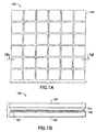
- Fig. 1A is an illustration of a top view of an array 100 of OLED structures, e.g., picture elements (pixels) or light emitting elements
- Fig. 1B is a side view of array 100 taken through line 1B - 1B of Fig. 1A .
- Each OLED structure of array 100 is constructed to have a pixel circuit that includes an OLED and a static memory for storing data that represents an operational state of the OLED.
- Array 100 may be generally considered to be a regular n x m array of pixels, where n may or may not be equal to m.
- Array 100 includes a plurality of OLED structures, each of which has an anode electrode 105.
- the anode electrodes 105 are arranged in two dimensions, forming a planar display.
- the side view shown in Fig. 1B depicts the vertical structure of array 100 on, by example, a silicon chip 101 upon which anode electrodes 105 are patterned.
- Disposed below anode electrodes 105 may be a light-blocking layer (not shown) to prevent OLED light or external light from reaching underlying circuitry.
- An organic layer 102 and a transparent cathode counter-electrode layer 103 are disposed above anode electrodes 105.
- an observer may view the OLED through its anode electrode 105, but the preferred embodiment involves viewing the OLED through its cathode counter-electrode layer 103. This is because the silicon substrate 101 is not transparent, but is opaque.
- a protective cover glass 104 is attached to the silicon chip 101 over cathode electrode layer 103 to provide environmental protection for the OLED structure.
- a suitable getter for moisture absorption may also be positioned within a cover-glass-to-silicon seal, but outside the boundary of array 100.
- data that defines a state of the pixels may be written to, and stored, in either a dynamic or static memory structure.
- the stored data may also be read out from the memory structure, if it is so configured, for example, for purposes of electrical testing.
- a dynamic memory array data is stored on a capacitor and must be refreshed periodically, an operation that dissipates power.
- a static memory data is stored in an electronic latch comprised of CMOS circuits, and virtually no power is dissipated to hold the data.
- the OLED display apparatus in accordance with the presently preferred embodiments of this invention uses static memory for low power dissipation.
- the organic material is sandwiched between pixel electrodes of the underlying circuit and a counter-electrode.
- the pixel electrode is typically the anode of the light emitting diode and the counter-electrode is typically the cathode.
- the display is formed as a rectangular array of pixels that are turned ON or OFF as the displayed image requires. Each pixel has a pixel anode electrode and pixel circuits that control the electrical state of the anode relative to the counter-electrode.
- the pixel circuits may be constructed using thin-films formed on an insulating substrate, or they may be constructed using integrated circuit technology, preferably silicon-based.
- the pixel circuit can be fabricated with (1) any suitable material, such as, for example, crystalline silicon, amorphous silicon, polysilicon, micro crystalline silicon, an organic semiconductor or a polymer semiconductor, and (2) disposed, for example, on a substrate of silicon, glass, plastic, ceramic, or sapphire (AL 2 O 3 ).
- the thin-film circuits on an insulating (dielectric) substrate have the advantages of lower cost and an ability to be fabricated into large displays.
- the use of crystalline silicon devices is confined to small area arrays, but the circuits have higher performance and higher fabrication density than the thin-film circuits.
- the OLED circuitry in accordance with these teachings is suitable for being implemented using a variety of fabrication techniques, but the crystalline silicon technology is the preferred embodiment. Since silicon substrates are opaque to visible light, light emission is preferably through the counter-electrode, which is preferably formed as a continuous sheet of transparent conductive material such as indium tin oxide, e.g., see counter-electrode layer 103.
- array is used to refer to an array of pixels as well as to an array of anodes.
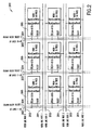
- Fig. 2 is a block diagram of an OLED array 200 comprising a plurality of data storage devices or units, also referred to herein as word structures 205.
- Each word structure 205 is a static random access memory (SRAM) of, for example, 16 bits that correspond to sixteen pixels along a row of array 200.
- SRAM static random access memory
- data is written into, and read out of, the array 16 bits at a time.
- each word structure 205 The inputs to each word structure 205 are a column block select 204, bit lines 203, a word line read 202 and a word line write 201. Data is written into word structure 205 from bit lines 203 when word line write 201 and column block select 204 lines are both activated, for example by switching them to a high state. Data is read from word structure 205 onto bit lines 203 when word line read 202 and column block select 204 are both activated. No operation is defined for the case where both word line read 202 and word line write 201 lines are active.
- each column block select 204 relates to a column of array 200, whereas each word line write 201 and word line read 202 relates to a row of array 200.
- word line writes 201 and word line reads 202 data can be written to, or read from, any of word structures 205 in array 200.
- the total number of bit lines 203 corresponds to the number of columns of pixels in array 200. Since each word structure 205 represents 16 pixels, the number of column block selects 204 corresponds to the number of columns of pixels in array 200 divided by 16.
- CMOS complementary metal-oxide-semiconductor
- CMOS complementary metal-oxide-semiconductor
- a set of bit lines 203 representing data bits 1 - 16 is configured as 16 single lines.
- reading data from the memory cells of a display is less efficient than reading from a system memory external to the display because reading from the display typically has higher power dissipation and lower speed.
- reading data from the memory cells of the display is useful when electrically testing the display. Nonetheless, an emphasis is placed on writing to the display rather than reading from the display. Accordingly, conventional SRAM design techniques such as pulsed word line addressing, bit line equalization and bit line sense circuitry are not required.
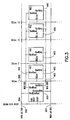
- Fig. 3 is a block diagram of an OLED pixel word structure 205.
- Word structure 205 includes a word select circuit 300 and sixteen pixel circuits 400.
- the inputs to word select circuit 300 are column block select 204, word line read 202 and word line write 201.
- the outputs of word select circuit 300 are word read 404 and word write 405.
- the inputs to pixel circuit 400 are a single bit line 203, word read 404 and word write 405.
- Word read 404 and word write 405 are the local word-selected extensions of word line read 202 and word line write 201, respectively.
- Word select circuit 300 is shown to the left of pixel circuits 400 by way of example.
- FIG. 4 shows the circuit details of some of the logic in word select circuit 300.
- Word select circuit 300 includes two AND gates 500 and 501.
- AND gate 500 The inputs to AND gate 500 are column block select 204 and word line read 202.
- Word read 404 is the output of AND gate 500. When both column block select 204 and word line read 202 are high, i.e., active, word read 404 goes high, i.e., active.
- AND gate 501 The inputs to AND gate 501 are column block select 204 and word line write 201.
- Word write 405 is the output of AND gate 501. When both column block select 204 and word line write 201 are high, i.e., active, word write 405 goes high, i.e., active.
- FIG. 5 is a simplified schematic of the major functional elements of pixel circuit 400 in array 200.
- Pixel circuit 400 includes an SRAM cell 10, a current source 20 connected to a voltage power supply V1, three switches 30, 40 and 50, a grounded gate p-type metal oxide semiconductor (PMOS) transistor 60 with its n-well connected to its source 64, i.e., a floating well, and an OLED 70 connected to a power supply voltage V2.
- PMOS metal oxide semiconductor
- V1 is a positive voltage
- V2 is a negative voltage.
- the inputs to SRAM cell 10 are a single bit line 203, word read 404, and word write 405.
- bit line 203 is a single bit line for inputting a signal that represents data to, and outputting a signal that represents the data from, SRAM cell 10.
- Word write 405 enables writing of data into SRAM cell 10
- word read 404 enables reading of data from SRAM cell 10.
- the outputs of SRAM cell 10 are bit line 203, and a control line 8.
- bit line 203 is both an input and an output of SRAM cell 10.
- Control line 8 is for controlling switch 40. With high states on both bit line 203 and word write 405, a high state is written into SRAM cell 10. When SRAM cell 10 stores a high state, control line 8 closes switch 40. When SRAM cell 10 stores a low state, control line 8 opens switch 40.
- V1 provides power for current source 20.
- Current source 20 produces an output current corresponding to a predetermined maximum brightness level of OLED 70.
- DUTY FACTOR NOT (6) is a pulse width modulated signal that is provided as an input common to all pixels in array 200. A low state on DUTY FACTOR NOT (6) closes switch 30. A high state on the DUTY FACTOR NOT (6) opens switch 30. The DUTY FACTOR NOT (6) controls the average current through OLED 70 to set its luminance to a level of less than the maximum brightness.
- a REVERSE BIAS (7) is a signal that is provided as an input common to all pixels in array 200. A high state on REVERSE BIAS (7) closes switch 50. A low state on REVERSE BIAS (7) opens switch 50.
- PMOS transistor 60 When switches 30 and 40 are closed and switch 50 is open, current flows from current source 20, through switches 30 and 40, and into source 64 of PMOS transistor 60.
- PMOS transistor 60 operates as a cascode stage to provide a greater voltage compliance range for current source 20, as is known in the art.
- Current out the drain 62 of PMOS transistor 60 flows into OLED 70 turning OLED 70 ON.
- Voltage compliance range is the range of output voltages over which the output current is essentially constant.
- a cascode stage is a common gate amplifier stage that improves the voltage compliance range by providing voltage gain.
- PMOS transistor 60 When current is flowing through PMOS transistor 60, it has a relatively low voltage, e.g., approximately 10 millivolts, across its drain 62 and source 64. With current flowing, the voltage on drain 62 can be several volts above or below ground while the voltage on source 64 is at a minimum of one threshold voltage above ground and always higher than the voltage on its drain 62. A threshold voltage is the minimum source to gate voltage required to maintain the transistor in the normal conducting region of operation. When no current is flowing into source 64 of PMOS transistor 60, the voltage on source 64 does not go below ground.
- a threshold voltage is the minimum source to gate voltage required to maintain the transistor in the normal conducting region of operation.
- charge can be trapped in its organic layers. This increases the forward bias voltage of the OLED required for a given current to flow.
- the trapped charge can be removed by reverse-biasing the OLED, either periodically or at irregular intervals.
- OLED 70 is reverse-biased by opening switch 30, thus interrupting flow of current from current source 20, closing switch 50 and switching V2 from a negative voltage to a positive voltage.
- Closing switch 50 grounds the source 64 and n-well of PMOS transistor 60.
- the drain 62 of PMOS transistor 60 is a p-diffusion.
- V2 is switched to a positive voltage, current flows from V2, through OLED 70 PMOS transistor 60 and switch 50.
- the anode 72 of OLED 70 is held at one diode voltage drop above ground.
- the reverse-bias voltage across OLED 70 is the positive voltage of V2 minus one diode drop.
- Reverse biasing of an OLED does not need to be performed at frequent intervals. Instead, it can be performed at irregular intervals or when a display is not being viewed.
- the OLED may be driven during the day in a normal forward bias manner, and at night, when the image on the display is OFF, the OLED voltage can be reverse-biased.
- the OLED can be reverse-biased during a pulse width modulation brightness control cycle when the OLED is turned OFF.
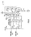
- FIG. 6 shows details of the pixel circuit 400 of FIG. 5 .
- V1 is set to +3V and V2 is set to -5V.
- SRAM cell 10 includes n-type metal oxide semiconductor (NMOS) transistors 11 and 15, and inverters 12, 13 and 14.
- NMOS metal oxide semiconductor
- a high state on word write input 405 causes NMOS transistor 11 to couple the logic state on bit line 203 to the input of inverter 12.
- inverter 12 The output of inverter 12 is an inverse of its input.
- the output of inverter 12 is connected to the input of inverter 13, and the input of inverter 14, and it also provides the signal for control line 8.
- Inverter 13 has its output connected to the input of inverter 12.
- inverter 12 receives its input either from bit line 203 by a turned ON NMOS transistor 11, or from the output of inverter 13.
- the current drive of NMOS transistor 11 is determined, in part, by a ratio of its channel width to its channel length.
- the current drives of inverter 12 and NMOS transistor 11 are relatively stronger, e.g., about 10 times stronger, than the drive of inverter 13. Accordingly, the input from bit line 203, by way of a turned ON NMOS transistor 11 to inverter 12, determines the state of SRAM cell 10.
- NMOS transistor 11 initially sets the state of inverter 12, and inverter 13 feeds back, i.e., provides a latch signal, into inverter 12 to hold the state after the data level from NMOS transistor 11 is removed.
- NMOS transistor 11, and inverters 12 and 13 comprise a data latch.
- a PMOS transistor 40A serves the role of switch 40 ( Fig. 5 ).
- Control line 8 from the output of inverter 12 is connected to the gate of PMOS transistor 40A.
- word read 404 is set high to cause NMOS transistor 15 to couple the output of inverter 14 to bit line 3.
- NMOS transistor 15 couples the output of inverter 14 to bit line 3.
- SRAM cell 10 may be simplified by eliminating inverter 14 and connecting the output of inverter 12 directly to NMOS transistor 15.
- the data read out of SRAM cell 10 is an inverse of that which was previously written into SRAM cell 10, but it can be re-inverted in a bit line read circuit (not shown).
- inverter 14 is included because it isolates pixel circuit 400 from noise on bit line 203 and from capacitance loading by bit line 203 during the read operation.
- a PMOS transistor 20A serves as a current source 20 ( Fig. 5 ).
- a VREF 21 is connected to the gate of PMOS transistor 20A, and also to a similarly situated PMOS transistor in all of the other pixel circuits of array 200.
- the previously mentioned light-blocking layer may, for instance, be used to distribute the +3V power of V1.
- the light-blocking layer a conducting layer, is distributed and connected throughout the array providing a low-resistance path for V1 power distribution. In this manner, the light-blocking layer performs two functions, i.e., light-blocking and power distribution.
- PMOS transistor 20A is a field effect transistor (FET) with a channel width (W), a channel length (L) and a gate to source voltage (V gs ) that are optimized within area constraints (- W x L) to minimize effects of threshold voltage (v r ) and channel width variations on the uniformity of current through OLED 70 of the pixels throughout the array.
- the channel length is determined by the separation of drain and source diffusions as formed by the gate conductor.
- the channel width is the drain or source dimension along the gate conductor. In saturation (
- VREF 21 voltage is set relative to V1 and is adjusted to obtain a desired measured maximum brightness of OLED 70, thereby removing the effect of current source transistor parameters and OLED efficiency on the overall maximum brightness of the display.
- the channel length is 2 ⁇ m (79.12 microns), the channel width is 67 nm (2.64 microns), and the gate to source voltage of PMOS transistor 20A is nominally -1.1 V.
- a threshold voltage of -0.6V PMOS transistor 20A remains in saturation, i.e., produces constant current, as long as its source to drain voltage is greater than 0.5V.
- the static source to gate voltage of PMOS transistor 20A is greater than its threshold voltage. In other words, only 0.5V of overhead voltage is required to drive OLED 70. In this regard, the design is very power efficient. With this implementation, the variation of current from PMOS transistor 20A, in pixels across the display, is less than 1.05:1.
- a PMOS transistor 30A serves the role of switch 30 ( Fig. 5 ), and an NMOS transistor 50A serves the role of switch 50 ( Fig. 5 ).
- This configuration of components allows the DUTY FACTOR NOT (6) and REVERSE BIAS (7) as shown in FIG. 5 to be combined in a single REVERSE BIAS/DUTY FACTOR NOT (9) signal.
- REVERSE BIAS/DUTY FACTOR NOT (9) is an input common to all pixels in array 200.
- REVERSE BIAS/DUTY FACTOR NOT 9 is duty factor modulated to turn PMOS transistor 30A ON and OFF rapidly, to duty factor modulate the current in OLED 70.
- This digital control of the brightness of OLED 70 is more uniform than controlling it by means of an analog voltage.
- NMOS transistor 50A is turned ON by REVERSE BIAS/DUTY FACTOR NOT (9) when PMOS transistor 30A is turned OFF to help linearize the pulse width modulation by discharging parasitic capacitances of transistors 20A, 30A, 40A, 50A and 60.
- the parasitic wiring, drain to substrate, source to substrate and FET interelectrode capacitances will allow current to continue to flow into the OLED for a short period while PMOS transistor 30A is OFF.
- the parasitic capacitances would tend to keep the voltage of PMOS transistor 60 source 64 high, allowing PMOS transistor 60 to continue conducting until source 64 is discharged.
- CMOS circuitry is susceptible to damage if it is exposed to a voltage exceeding a its breakdown voltage, which is typically 3.6V. Also, the lifespan of the organic layers is significantly shortened when subjected to temperatures greater than 100 degrees centigrade. If an OLED is shorted between its anode and cathode, then an excessive current may flow through the shorted OLED's pixel circuit. Such a current may generate heat and damage an adjacent pixel, and it may also interfere with the voltages supplied to other pixels in the display.
- pixel circuit 400 includes a protection circuit comprising PMOS transistors 81, 82 and 83, and a resistor 84.
- PMOS transistors 81, 82 and 83 When the pixel is in the OFF state, the voltage drop across OLED 70 is reduced so the voltage at drain 62 of PMOS transistor 60 becomes more negative.
- Each of PMOS transistors 81, 82 and 83 drops approximately 1V, so that the voltage at source 64 of PMOS transistor 60 is limited to about 3 volts more negative than ground. That is, PMOS transistors 81, 82 and 83 provide a negative (-3V) voltage clamp to assure that the gate to drain voltage of PMOS transistor 60 does not exceed its breakdown voltage rating of 3.6V.
- the protection circuit effectively limits the current that can flow through the other components of pixel circuit 400.
- the voltage at drain 62 is about 1.75V above ground.
- PMOS transistors 81, 82 and 83 have no effect when OLED 70 is ON.
- resistor 84 limits the current that can flow, and the power that can be dissipated.
- PMOS transistors 81, 82 and 83 still clamp the voltage at drain 62 of PMOS transistor 60 to approximately -3 volts, and any excess voltage is dropped across resistor 84.
- resistor 84 is manufactured of undoped polysilicon having 40,000 ohms of resistance.
- PMOS transistors 81, 82 and 83, and resistor 84 also allow testing of OLED 70, and through similarly situated components in other pixel circuits, all of the OLED pixels in array 200. This done by setting V2 to a negative voltage, e.g., -7V, with respect to ground, and either allowing V1 to float or setting it to ground. With this arrangement, current path is created from ground through PMOS transistors 81, 82 and 83, resistor 84, OLED 70 to V2. Each of PMOS transistors 81, 82 and 83 drop about 0.7V. OLED 70 is forward biased, and if it is good, then it turns ON. This test is useful, for example, to spot defects after OLED deposition and sealing prior to further assembly of the display.
- power can be saved by managing the manner in which images are written to a display.
- display power dissipation is proportional to the brightness of a pixel, and the number of pixels that are ON, therefore a strategy to reduce the brightness of a pixel and the number pixels that are ON would result in a saving of power.
- array 200 is installed in a display for a wristwatch, then the number of pixels required to show the time as hands of a clock is between 1 and 2% of the total number of pixels.
- a typical screen for text might turn ON 10 to 20% of the pixels. Images may require an illumination of 50% of the pixels.
- gray scale images are produced by spatial dithering as opposed to frame sequential operation to eliminate the power required to write rapidly to the display, as would be required for frame sequential operation.
- the number of ON pixels is usually less than 50%, and therefore power can be saved by clearing the display in one operation before writing new data to the display and by only writing to word structures that have pixels turned ON.
- the full display can be cleared using bit line and word line driver circuits outside the array. If all word line writes 201 and column block selects 204 are brought high, with low data states on all bit lines 203, then low level data is written into all SRAM cells 10 in array 200 turning OFF all the pixels in the display. In the example of a wristwatch, the control for this function is issued by the watch processor prior to updating the display. Then, data is written only to pixels that need to be ON in the new displayed screen.
- the brightness when showing time can be reduced to a relatively low luminance level, e.g., about 30 candelas/meter squared.
- This luminance level should be sufficient for nighttime use and for low contrast applications at room ambient light levels. For showing text and images in room ambient conditions, 100 candelas/meter squared should be sufficient. Only use in bright sunlight conditions require luminance levels of 500 candelas/meter squared.
- the REVERSE BIAS/DUTY FACTOR NOT (9) should be in a high state.
- the connection of V2 to the display should be opened to eliminate any OFF state OLED current or currents due to OLED shorts. Accordingly, the current path between V1 and V2 is broken so that no current flows through pixel circuit 400.
- the standby current draw of SRAM cell 10 can be reduced if the voltage of V1 is reduced, but not set so low that the display losses its data. Lowering the supply voltage reduces the leakage current through inverters 12, 13 and 14, and thus lowers standby power.
- the control for standby is provided by the watch processor.
- the control signals for DUTY FACTOR NOT (6), REVERSE BIAS (7), standby and clear can be written into an a SRAM word structure that forms a display control register, as described below, that is not part of array 200, but external to it. In this manner, the display control signals are part of the display and not located elsewhere in the watch, thus reducing the number of dedicated signal lines to the display.
- control register One function of the control register is to "clear" the display, i.e., turn all pixels OFF in one operation. That is, to clear the displayed image without addressing all of the individual pixels of the display. This is done so that the processor need write only the pixels that will be ON in the new image, thus reducing power dissipation and burden on the processor compared to writing all pixels of the display.
- FIG. 7 shows the functional blocks of the display involved in writing to and reading from array 200 and a display control register 705, and the control flow for the clear operation.
- the processor (not shown) writes a word into display control register 705 including one bit that is dedicated to the clear function.
- a word has 16 bits.
- the processor sends addresses, a read/write signal, a chip select signal, and image data to the display.
- one column select line 204 ( Fig. 2 ) is activated by a column block decoder 701
- one word line read 202 ( Fig. 2 ) or one word line write 201 ( Fig. 2 ) is activated by a word line decoder 702
- appropriate bit lines 203 ( Fig. 2 ) are selected by bit line read/write drivers 703.
- display control register 705 is addressed for writing by the column block decoder 701 and word line decoder 702, and the data bit for clear is applied to the bit line read/write drivers 703 and stored in display control register 705.
- a clear line output 704 of display control register 705 is then activated, applying a clear signal to column block decoder 701, word line decoder 702 and bit line read/write drivers 703, which causes a "zero" to be written to all pixels of array 200 simultaneously, turning OFF all OLEDs.
- the display is designed to be addressed by the memory expansion bus of a microprocessor which transmits image data to the display in the form of words, each comprising the data for several pixels at a time, for example, 16 pixels at a time. Data may also be read out of the SRAM storage of the display, for instance for testing purposes, also a word at a time.
- word select circuits are embedded in the display, for example, one such circuit for every horizontal group of 16 pixels. This necessitates a periodic shifting of the connections between the pixel circuits and the actual pixels to maintain a uniform, or constant, pixel pitch.
- Fig. 8 is a block diagram of an OLED pixel word structure 205 showing a physical relationship of pixel circuits 400 and a word select circuit 300 to respective anodes of OLED pixels.
- Word structure 205 is comprised of 16 pixel circuits 400 and one word select circuit 300 disposed along a row of array 200.
- 16 OLED anode electrodes 105 overlay word structure 205, each anode being connected by a conductive via 802 to a metal conductor 801 of a corresponding pixel circuit 400.
- Via 802 and conductor 801 are part of a conductive path from pixel circuit 400 to anode 105, i.e. a connection from resistor 84 to OLED 70 in Fig. 6 .
- anode electrodes 105 and pixel circuits 400 are shown adjacent to each other for clarity, it will be clear that in practice they overlap each other, at least in part.
- the average row-wise dimension of pixel circuit 400 and the pitch of anode electrode 105 are 871 nm (34.3 microns), while the row-wise pitch of word select circuit 300 is 203 nm (8 microns).
- each pixel circuit 400 In order for the 16 pixel circuits 400 and one word select circuit 300 to occupy the same horizontal space as the 16 anode electrodes 105, the row-wise dimension of each pixel circuit 400 is reduced by 12.7 nm (0.5 microns), i.e., from 871 nm (34.3 microns) to 859 nm (33.8 microns), as compared to the anode electrodes 105.
- via 802 should be centered on each anode electrode 105, or at least be located at the same relative position on each anode electrode 105.
- conductor 801 of each pixel circuit 400 has a sufficient row-wise extent to accommodate the shifting position of via 802. The result is that the pitch of the OLED anodes is uniform throughout the array even though the pitch of the pixel circuits, to which the OLED anodes are connected, is not uniform.
- CMOS circuits are incorporated into each pixel of an active matrix OLED display.
- the circuits exhibit low power dissipation for battery operation, incorporate a constant current source for uniformity of brightness and reduced dependence of brightness on the characteristics of the OLED, and permit the use of a lower voltage circuit technology than the voltage which the OLED requires for operation.
- Each pixel incorporates an SRAM memory cell to control the state, ON or OFF, of the pixel and so does not require periodic refreshing.
- the circuit also has a provision for application of reverse voltage when required to minimize deterioration of the OLED over time, a provision for duty factor control of luminance, and a current limiting resistor to isolate the effect of shorted pixels.
- the display is addressed by the memory expansion bus of a microprocessor in the form of words of several pixels length, and the display data may be read out in the same form. Circuits for decoding the word address are embedded in the array of pixels that comprise the display. Furthermore, a provision is made to clear the display image in one operation so that a new image may be displayed by addressing only the pixels that are turned ON.
Abstract
Description
- This invention relates generally to a pixel circuit, and, more particularly, to a low-power organic light emitting diode (OLED) pixel circuit utilizing complementary metal oxide semiconductor (CMOS) technology.
- An OLED pixel may utilize any of a variety of organic materials that emit light when an electric current is applied thereto. An OLED display comprises a plurality of OLED pixels organized into an array.
- Illumination of an OLED pixel is controlled by a pixel circuit that may include either a constant current source or a constant voltage source. It is generally recognized that the constant current source provides a greater uniformity of luminance among the pixels of the array. This is because the dependence of luminance upon current tends to be uniform while the voltage across the OLEDs at a given current in the various pixels tends to be less uniform.
US Patent No. 6,023,259 to Howard et al . describes a current driver that provides a passive matrix drive current to an OLED. For typical display brightness, passive matrix drive operation results in lower OLED power efficiency and, in order to avoid flicker, requires a refresh rate greater than or equal to 60 Hz. - In an active matrix display, a provision is generally made for storage of the state of a pixel within its respective pixel circuit. This is commonly achieved by incorporating the equivalent of a dynamic RAM cell in each pixel circuit, in which the state is stored as a voltage across a capacitor. A disadvantage of such an arrangement is that the voltage quickly bleeds off the capacitors, and consequently any image represented on the display must be regularly refreshed. This act of refreshing the image consumes a significant quantity of power. It is therefore desirable to find an alternative to the conventional use of dynamic RAMs.
- Control of the luminance of an "on" pixel is commonly achieved by controlling a magnitude of an analog voltage that determines the voltage or current applied to the pixel. Analog control circuits are another source of excessive power dissipation. It is therefore desirable to find an alternative to the conventional use of analog control circuitry.
- The OLED display is constructed of thin layers of organic material in which individual OLED pixels are subject to an occasional short circuit between an anode of the OLED and a counter-electrode of the OLED. Such a short can cause excess current to flow in the circuit, excess voltage across the pixel circuit and excess power dissipation. Good pixels neighboring a shorted pixel may be destroyed by heat from the shorted pixel and the excess current may alter power supply voltages.
- During operation of the OLED display, the layers of organic material tend to trap charge, causing increases in the voltage drop across the OLED, which can cause a non-uniformity of luminance and a burned-in image. The trapped charge may be removed by reverse-biasing the OLED.
- The OLED itself typically requires a voltage on the order of +/- 6 volts to develop an adequate luminance when turned ON and to remove trapped charge when reverse-biased. Conventional CMOS integrated circuit technology uses transistors that operate with a voltage of less than 4 volts. Accordingly, CMOS technology is not ordinarily capable of driving an OLED. Furthermore, a CMOS device in an OLED pixel circuit is particularly susceptible to damage from the voltage in excess of 4 volts.
- A traditional manner of changing a displayed image is for a processor to update the memory of a display controller that periodically and individually addresses each of the pixels of the display, and turn them "on" (ON) and "off" (OFF) as required. If the display included a large number of pixels, for example one hundred thousand, one million, or more, this operation would consume a significant quantity of power and could burden the processor.
- An additional problem when incorporating a plurality of pixel circuits into a display is that of physically distributing the collective elements of the display. That is, the display is a finite area within which the pixels and their accompanying circuitry are confined, yet a constant pitch between pixels must be maintained in order to provide a uniform image.
- Because of the aforementioned disadvantages, OLED displays have not been as readily adopted by designers as have many other conventional display technologies. The use of dynamic RAM and its corresponding circuitry required for refreshing an image, and issues relating to power dissipation are an obstacle to an employment of OLEDs in battery operated devices, and in small displays such as those used for hand-held devices or watches. The OLED operating voltages are an obstacle to the use of CMOS circuitry in an OLED pixel circuit. The regular addressing of every pixel in an array is an obstacle to the employment of OLEDs in large displays. The maintenance of a constant pitch between pixels is an important consideration in any display.
- Document
EP-A-0365445 describes a pixel circuit with an organic electroluminescent element and a memory cell with two CMOS inventers. - The invention is set forth in attached
claim 1. - The invention will now be described, by way of example only, with reference to the accompanying drawings, in which:
-
Fig. 1A is an illustration of a top view of an array of OLED structures, in accordance with the teachings of this invention; -
Fig. 1B is a side view of the array ofFig. 1A taken throughline 1B - 1B; -
Fig. 2 is a block diagram of an OLED pixel word array structure, each word being composed of 16 pixels; -
Fig. 3 is a block diagram of an embodiment of an OLED pixel word circuit; -
Fig. 4 is schematic of logic circuitry in a word select circuit, in accordance with these teachings; -
Fig. 5 is a simplified schematic of an embodiment of an OLED pixel circuit; -
Fig. 6 is a more detailed schematic of an OLED pixel circuit; -
Fig. 7 is a block diagram of display and control register clear connections for driving an OLED array; and -
Fig. 8 is a block diagram of an OLED pixel word structure showing a physical relationship of pixel circuits and a word select circuit to respective anodes of OLED pixels. - The teachings in accordance with presently preferred embodiments of this invention relate to active matrix OLED displays. Such displays may be configured as micro-displays and incorporated into small, battery-powered devices such as electronic wristwatches. This particular field of use and application should not, however, be construed in any manner as a limitation upon the practice of the teachings of this invention.
-
Fig. 1A is an illustration of a top view of anarray 100 of OLED structures, e.g., picture elements (pixels) or light emitting elements, andFig. 1B is a side view ofarray 100 taken throughline 1B - 1B ofFig. 1A . Each OLED structure ofarray 100 is constructed to have a pixel circuit that includes an OLED and a static memory for storing data that represents an operational state of the OLED. -
Array 100 may be generally considered to be a regular n x m array of pixels, where n may or may not be equal to m. -
Array 100 includes a plurality of OLED structures, each of which has ananode electrode 105. Theanode electrodes 105 are arranged in two dimensions, forming a planar display. The side view shown inFig. 1B depicts the vertical structure ofarray 100 on, by example, asilicon chip 101 upon whichanode electrodes 105 are patterned. Disposed belowanode electrodes 105 may be a light-blocking layer (not shown) to prevent OLED light or external light from reaching underlying circuitry. Anorganic layer 102 and a transparentcathode counter-electrode layer 103 are disposed aboveanode electrodes 105. - In some OLED displays with a transparent anode, an observer may view the OLED through its
anode electrode 105, but the preferred embodiment involves viewing the OLED through itscathode counter-electrode layer 103. This is because thesilicon substrate 101 is not transparent, but is opaque. - A
protective cover glass 104 is attached to thesilicon chip 101 overcathode electrode layer 103 to provide environmental protection for the OLED structure. A suitable getter for moisture absorption may also be positioned within a cover-glass-to-silicon seal, but outside the boundary ofarray 100. - In an active matrix scheme of addressing the display, data that defines a state of the pixels, that is, whether the pixel is ON, i.e., luminous, or OFF, i.e., dark, may be written to, and stored, in either a dynamic or static memory structure. The stored data may also be read out from the memory structure, if it is so configured, for example, for purposes of electrical testing. In a dynamic memory array, data is stored on a capacitor and must be refreshed periodically, an operation that dissipates power. In a static memory, data is stored in an electronic latch comprised of CMOS circuits, and virtually no power is dissipated to hold the data. The OLED display apparatus in accordance with the presently preferred embodiments of this invention uses static memory for low power dissipation.
- In an active matrix display in accordance with these teachings the organic material is sandwiched between pixel electrodes of the underlying circuit and a counter-electrode. The pixel electrode is typically the anode of the light emitting diode and the counter-electrode is typically the cathode. The display is formed as a rectangular array of pixels that are turned ON or OFF as the displayed image requires. Each pixel has a pixel anode electrode and pixel circuits that control the electrical state of the anode relative to the counter-electrode.
- The pixel circuits may be constructed using thin-films formed on an insulating substrate, or they may be constructed using integrated circuit technology, preferably silicon-based. In general, the pixel circuit can be fabricated with (1) any suitable material, such as, for example, crystalline silicon, amorphous silicon, polysilicon, micro crystalline silicon, an organic semiconductor or a polymer semiconductor, and (2) disposed, for example, on a substrate of silicon, glass, plastic, ceramic, or sapphire (AL2O3). The thin-film circuits on an insulating (dielectric) substrate have the advantages of lower cost and an ability to be fabricated into large displays. In general, the use of crystalline silicon devices is confined to small area arrays, but the circuits have higher performance and higher fabrication density than the thin-film circuits. The OLED circuitry in accordance with these teachings is suitable for being implemented using a variety of fabrication techniques, but the crystalline silicon technology is the preferred embodiment. Since silicon substrates are opaque to visible light, light emission is preferably through the counter-electrode, which is preferably formed as a continuous sheet of transparent conductive material such as indium tin oxide, e.g., see
counter-electrode layer 103. - In the description that follows, the term "array" is used to refer to an array of pixels as well as to an array of anodes.
-
Fig. 2 is a block diagram of anOLED array 200 comprising a plurality of data storage devices or units, also referred to herein asword structures 205. Eachword structure 205 is a static random access memory (SRAM) of, for example, 16 bits that correspond to sixteen pixels along a row ofarray 200. In this embodiment data is written into, and read out of, thearray 16 bits at a time. - The inputs to each
word structure 205 are a column block select 204,bit lines 203, a word line read 202 and aword line write 201. Data is written intoword structure 205 frombit lines 203 whenword line write 201 and column block select 204 lines are both activated, for example by switching them to a high state. Data is read fromword structure 205 ontobit lines 203 when word line read 202 and column block select 204 are both activated. No operation is defined for the case where both word line read 202 and word line write 201 lines are active. - Note that each column block select 204 relates to a column of
array 200, whereas eachword line write 201 and word line read 202 relates to a row ofarray 200. By using an appropriate combination of column block selects 204, word line writes 201 and word line reads 202, data can be written to, or read from, any ofword structures 205 inarray 200. - The total number of
bit lines 203 corresponds to the number of columns of pixels inarray 200. Since eachword structure 205 represents 16 pixels, the number of column block selects 204 corresponds to the number of columns of pixels inarray 200 divided by 16. - Conventional SRAMs typically use complimentary bit lines, i.e., two lines per bit. The present invention uses a single bit line per pixel column, thus reducing power dissipation as compared to the conventional design. For example, in
Fig. 2 , a set ofbit lines 203 representing data bits 1 - 16 is configured as 16 single lines. - From a system point of view, reading data from the memory cells of a display is less efficient than reading from a system memory external to the display because reading from the display typically has higher power dissipation and lower speed. However, reading data from the memory cells of the display is useful when electrically testing the display. Nonetheless, an emphasis is placed on writing to the display rather than reading from the display. Accordingly, conventional SRAM design techniques such as pulsed word line addressing, bit line equalization and bit line sense circuitry are not required.
-
Fig. 3 is a block diagram of an OLEDpixel word structure 205.Word structure 205 includes a wordselect circuit 300 and sixteenpixel circuits 400. The inputs to wordselect circuit 300 are column block select 204, word line read 202 andword line write 201. The outputs of wordselect circuit 300 are word read 404 and word write 405. The inputs topixel circuit 400 are asingle bit line 203, word read 404 and word write 405. Word read 404 and word write 405 are the local word-selected extensions of word line read 202 andword line write 201, respectively. Wordselect circuit 300 is shown to the left ofpixel circuits 400 by way of example. -
FIG. 4 shows the circuit details of some of the logic in wordselect circuit 300. Wordselect circuit 300 includes two ANDgates - The inputs to AND
gate 500 are column block select 204 and word line read 202. Word read 404 is the output of ANDgate 500. When both column block select 204 and word line read 202 are high, i.e., active, word read 404 goes high, i.e., active. - The inputs to AND
gate 501 are column block select 204 andword line write 201. Word write 405 is the output of ANDgate 501. When both column block select 204 andword line write 201 are high, i.e., active, word write 405 goes high, i.e., active. -
FIG. 5 is a simplified schematic of the major functional elements ofpixel circuit 400 inarray 200.Pixel circuit 400 includes anSRAM cell 10, acurrent source 20 connected to a voltage power supply V1, threeswitches transistor 60 with its n-well connected to itssource 64, i.e., a floating well, and anOLED 70 connected to a power supply voltage V2. During normal operation V1 is a positive voltage and V2 is a negative voltage. - The inputs to
SRAM cell 10 are asingle bit line 203, word read 404, and word write 405. Note thatbit line 203 is a single bit line for inputting a signal that represents data to, and outputting a signal that represents the data from,SRAM cell 10. Word write 405 enables writing of data intoSRAM cell 10 and word read 404 enables reading of data fromSRAM cell 10. The outputs ofSRAM cell 10 arebit line 203, and acontrol line 8. Note thatbit line 203 is both an input and an output ofSRAM cell 10.Control line 8 is for controllingswitch 40. With high states on bothbit line 203 and word write 405, a high state is written intoSRAM cell 10. WhenSRAM cell 10 stores a high state,control line 8 closes switch 40. WhenSRAM cell 10 stores a low state,control line 8 opensswitch 40. - V1 provides power for
current source 20.Current source 20 produces an output current corresponding to a predetermined maximum brightness level ofOLED 70. - It is desirable to control the luminance of
OLED 70 by controlling the average current throughOLED 70. DUTY FACTOR NOT (6) is a pulse width modulated signal that is provided as an input common to all pixels inarray 200. A low state on DUTY FACTOR NOT (6) closesswitch 30. A high state on the DUTY FACTOR NOT (6) opensswitch 30. The DUTY FACTOR NOT (6) controls the average current throughOLED 70 to set its luminance to a level of less than the maximum brightness. - A REVERSE BIAS (7) is a signal that is provided as an input common to all pixels in
array 200. A high state on REVERSE BIAS (7) closesswitch 50. A low state on REVERSE BIAS (7) opensswitch 50. - When switches 30 and 40 are closed and switch 50 is open, current flows from
current source 20, throughswitches source 64 ofPMOS transistor 60.PMOS transistor 60 operates as a cascode stage to provide a greater voltage compliance range forcurrent source 20, as is known in the art. Current out thedrain 62 ofPMOS transistor 60 flows intoOLED 70 turningOLED 70 ON. Voltage compliance range is the range of output voltages over which the output current is essentially constant. A cascode stage is a common gate amplifier stage that improves the voltage compliance range by providing voltage gain. - When current is flowing through
PMOS transistor 60, it has a relatively low voltage, e.g., approximately 10 millivolts, across itsdrain 62 andsource 64. With current flowing, the voltage ondrain 62 can be several volts above or below ground while the voltage onsource 64 is at a minimum of one threshold voltage above ground and always higher than the voltage on itsdrain 62. A threshold voltage is the minimum source to gate voltage required to maintain the transistor in the normal conducting region of operation. When no current is flowing intosource 64 ofPMOS transistor 60, the voltage onsource 64 does not go below ground. - During operation of an OLED, charge can be trapped in its organic layers. This increases the forward bias voltage of the OLED required for a given current to flow. The trapped charge can be removed by reverse-biasing the OLED, either periodically or at irregular intervals.
-
OLED 70 is reverse-biased by openingswitch 30, thus interrupting flow of current fromcurrent source 20, closingswitch 50 and switching V2 from a negative voltage to a positive voltage. Closingswitch 50 grounds thesource 64 and n-well ofPMOS transistor 60. Thedrain 62 ofPMOS transistor 60 is a p-diffusion. When V2 is switched to a positive voltage, current flows from V2, throughOLED 70PMOS transistor 60 andswitch 50. ThroughPMOS transistor 60 andclosed switch 50, theanode 72 ofOLED 70 is held at one diode voltage drop above ground. The reverse-bias voltage acrossOLED 70 is the positive voltage of V2 minus one diode drop. - Reverse biasing of an OLED does not need to be performed at frequent intervals. Instead, it can be performed at irregular intervals or when a display is not being viewed. For example, in a wristwatch display, the OLED may be driven during the day in a normal forward bias manner, and at night, when the image on the display is OFF, the OLED voltage can be reverse-biased. As another example, the OLED can be reverse-biased during a pulse width modulation brightness control cycle when the OLED is turned OFF.
-
FIG. 6 shows details of thepixel circuit 400 ofFIG. 5 . In this embodiment, V1 is set to +3V and V2 is set to -5V. -
SRAM cell 10 includes n-type metal oxide semiconductor (NMOS)transistors 11 and 15, andinverters input 405 causes NMOS transistor 11 to couple the logic state onbit line 203 to the input ofinverter 12. - The output of
inverter 12 is an inverse of its input. The output ofinverter 12 is connected to the input ofinverter 13, and the input ofinverter 14, and it also provides the signal forcontrol line 8. -
Inverter 13 has its output connected to the input ofinverter 12. Note thatinverter 12 receives its input either frombit line 203 by a turned ON NMOS transistor 11, or from the output ofinverter 13. The current drive of NMOS transistor 11 is determined, in part, by a ratio of its channel width to its channel length. The current drives ofinverter 12 and NMOS transistor 11 are relatively stronger, e.g., about 10 times stronger, than the drive ofinverter 13. Accordingly, the input frombit line 203, by way of a turned ON NMOS transistor 11 toinverter 12, determines the state ofSRAM cell 10. A data level through NMOS transistor 11 initially sets the state ofinverter 12, andinverter 13 feeds back, i.e., provides a latch signal, intoinverter 12 to hold the state after the data level from NMOS transistor 11 is removed. Thus, NMOS transistor 11, andinverters - A
PMOS transistor 40A serves the role of switch 40 (Fig. 5 ).Control line 8, from the output ofinverter 12, is connected to the gate ofPMOS transistor 40A. - To read data from
SRAM cell 10, word read 404 is set high to causeNMOS transistor 15 to couple the output ofinverter 14 tobit line 3. Through the inversions ofinverter 12 andinverter 14, the polarity of data read out ofSRAM cell 10 is the same as that previously written intoSRAM cell 10. -
SRAM cell 10 may be simplified by eliminatinginverter 14 and connecting the output ofinverter 12 directly toNMOS transistor 15. In such a case, the data read out ofSRAM cell 10 is an inverse of that which was previously written intoSRAM cell 10, but it can be re-inverted in a bit line read circuit (not shown). Preferably,inverter 14 is included because it isolatespixel circuit 400 from noise onbit line 203 and from capacitance loading bybit line 203 during the read operation. - A
PMOS transistor 20A serves as a current source 20 (Fig. 5 ). AVREF 21 is connected to the gate ofPMOS transistor 20A, and also to a similarly situated PMOS transistor in all of the other pixel circuits ofarray 200. - The previously mentioned light-blocking layer may, for instance, be used to distribute the +3V power of V1. The light-blocking layer, a conducting layer, is distributed and connected throughout the array providing a low-resistance path for V1 power distribution. In this manner, the light-blocking layer performs two functions, i.e., light-blocking and power distribution.
-
PMOS transistor 20A is a field effect transistor (FET) with a channel width (W), a channel length (L) and a gate to source voltage (Vgs) that are optimized within area constraints (- W x L) to minimize effects of threshold voltage (vr) and channel width variations on the uniformity of current throughOLED 70 of the pixels throughout the array. The channel length is determined by the separation of drain and source diffusions as formed by the gate conductor. The channel width is the drain or source dimension along the gate conductor. In saturation

where Vds is the drain to source voltage.VREF 21 voltage is set relative to V1 and is adjusted to obtain a desired measured maximum brightness ofOLED 70, thereby removing the effect of current source transistor parameters and OLED efficiency on the overall maximum brightness of the display. - In an exemplary implementation of
PMOS transistor 20A, the channel length is 2µm (79.12 microns), the channel width is 67 nm (2.64 microns), and the gate to source voltage ofPMOS transistor 20A is nominally -1.1 V. With a threshold voltage of -0.6V,PMOS transistor 20A remains in saturation, i.e., produces constant current, as long as its source to drain voltage is greater than 0.5V. Note that the static source to gate voltage ofPMOS transistor 20A is greater than its threshold voltage. In other words, only 0.5V of overhead voltage is required to driveOLED 70. In this regard, the design is very power efficient. With this implementation, the variation of current fromPMOS transistor 20A, in pixels across the display, is less than 1.05:1. - A
PMOS transistor 30A serves the role of switch 30 (Fig. 5 ), and anNMOS transistor 50A serves the role of switch 50 (Fig. 5 ). This configuration of components allows the DUTY FACTOR NOT (6) and REVERSE BIAS (7) as shown inFIG. 5 to be combined in a single REVERSE BIAS/DUTY FACTOR NOT (9) signal. REVERSE BIAS/DUTY FACTOR NOT (9) is an input common to all pixels inarray 200. - In normal forward biased operation of
OLED 70, REVERSE BIAS/DUTY FACTOR NOT (9) is duty factor modulated to turnPMOS transistor 30A ON and OFF rapidly, to duty factor modulate the current inOLED 70. This digital control of the brightness ofOLED 70 is more uniform than controlling it by means of an analog voltage.NMOS transistor 50A is turned ON by REVERSE BIAS/DUTY FACTOR NOT (9) whenPMOS transistor 30A is turned OFF to help linearize the pulse width modulation by discharging parasitic capacitances oftransistors PMOS transistor 30A is OFF. The parasitic capacitances would tend to keep the voltage ofPMOS transistor 60source 64 high, allowingPMOS transistor 60 to continue conducting untilsource 64 is discharged. - CMOS circuitry is susceptible to damage if it is exposed to a voltage exceeding a its breakdown voltage, which is typically 3.6V. Also, the lifespan of the organic layers is significantly shortened when subjected to temperatures greater than 100 degrees centigrade. If an OLED is shorted between its anode and cathode, then an excessive current may flow through the shorted OLED's pixel circuit. Such a current may generate heat and damage an adjacent pixel, and it may also interfere with the voltages supplied to other pixels in the display.
- Accordingly,
pixel circuit 400 includes a protection circuit comprisingPMOS transistors resistor 84. During normal operation, when the pixel is in the OFF state, the voltage drop acrossOLED 70 is reduced so the voltage atdrain 62 ofPMOS transistor 60 becomes more negative. Each ofPMOS transistors source 64 ofPMOS transistor 60 is limited to about 3 volts more negative than ground. That is,PMOS transistors PMOS transistor 60 does not exceed its breakdown voltage rating of 3.6V. By limiting the voltage atdrain 62 ofPMOS transistor 60, the protection circuit effectively limits the current that can flow through the other components ofpixel circuit 400. WhenOLED 70 is ON, the voltage atdrain 62 is about 1.75V above ground.PMOS transistors OLED 70 is ON. - In the case where
OLED 70 is shorted,resistor 84 limits the current that can flow, and the power that can be dissipated.PMOS transistors drain 62 ofPMOS transistor 60 to approximately -3 volts, and any excess voltage is dropped acrossresistor 84. In a preferred embodiment,resistor 84 is manufactured of undoped polysilicon having 40,000 ohms of resistance. -
PMOS transistors resistor 84 also allow testing ofOLED 70, and through similarly situated components in other pixel circuits, all of the OLED pixels inarray 200. This done by setting V2 to a negative voltage, e.g., -7V, with respect to ground, and either allowing V1 to float or setting it to ground. With this arrangement, current path is created from ground throughPMOS transistors resistor 84,OLED 70 to V2. Each ofPMOS transistors V. OLED 70 is forward biased, and if it is good, then it turns ON. This test is useful, for example, to spot defects after OLED deposition and sealing prior to further assembly of the display. - In addition to the techniques for saving power mentioned above, power can be saved by managing the manner in which images are written to a display. For example, display power dissipation is proportional to the brightness of a pixel, and the number of pixels that are ON, therefore a strategy to reduce the brightness of a pixel and the number pixels that are ON would result in a saving of power.
- For example, if
array 200 is installed in a display for a wristwatch, then the number of pixels required to show the time as hands of a clock is between 1 and 2% of the total number of pixels. A typical screen for text might turn ON 10 to 20% of the pixels. Images may require an illumination of 50% of the pixels. - Accordingly, gray scale images are produced by spatial dithering as opposed to frame sequential operation to eliminate the power required to write rapidly to the display, as would be required for frame sequential operation.
- The number of ON pixels is usually less than 50%, and therefore power can be saved by clearing the display in one operation before writing new data to the display and by only writing to word structures that have pixels turned ON. The full display can be cleared using bit line and word line driver circuits outside the array. If all word line writes 201 and column block selects 204 are brought high, with low data states on all
bit lines 203, then low level data is written into allSRAM cells 10 inarray 200 turning OFF all the pixels in the display. In the example of a wristwatch, the control for this function is issued by the watch processor prior to updating the display. Then, data is written only to pixels that need to be ON in the new displayed screen. - Since a watch display typically displays time 99% of the time and since the watch hands that indicate the time do not require high contrast, the brightness when showing time can be reduced to a relatively low luminance level, e.g., about 30 candelas/meter squared. This luminance level should be sufficient for nighttime use and for low contrast applications at room ambient light levels. For showing text and images in room ambient conditions, 100 candelas/meter squared should be sufficient. Only use in bright sunlight conditions require luminance levels of 500 candelas/meter squared.
- To save power during a watch system standby function, the REVERSE BIAS/DUTY FACTOR NOT (9) should be in a high state. In addition, the connection of V2 to the display should be opened to eliminate any OFF state OLED current or currents due to OLED shorts. Accordingly, the current path between V1 and V2 is broken so that no current flows through
pixel circuit 400. - Also, the standby current draw of
SRAM cell 10 can be reduced if the voltage of V1 is reduced, but not set so low that the display losses its data. Lowering the supply voltage reduces the leakage current throughinverters - The control signals for DUTY FACTOR NOT (6), REVERSE BIAS (7), standby and clear can be written into an a SRAM word structure that forms a display control register, as described below, that is not part of
array 200, but external to it. In this manner, the display control signals are part of the display and not located elsewhere in the watch, thus reducing the number of dedicated signal lines to the display. - One function of the control register is to "clear" the display, i.e., turn all pixels OFF in one operation. That is, to clear the displayed image without addressing all of the individual pixels of the display. This is done so that the processor need write only the pixels that will be ON in the new image, thus reducing power dissipation and burden on the processor compared to writing all pixels of the display.
-
FIG. 7 shows the functional blocks of the display involved in writing to and reading fromarray 200 and adisplay control register 705, and the control flow for the clear operation. The processor (not shown) writes a word into display control register 705 including one bit that is dedicated to the clear function. In the exemplary embodiment shown inFig. 7 , a word has 16 bits. - In operation, the processor sends addresses, a read/write signal, a chip select signal, and image data to the display. For each address and data word received, one column select line 204 (
Fig. 2 ) is activated by acolumn block decoder 701, one word line read 202 (Fig. 2 ) or one word line write 201 (Fig. 2 ) is activated by aword line decoder 702, and appropriate bit lines 203 (Fig. 2 ) are selected by bit line read/writedrivers 703. If a clear operation is to be performed,display control register 705 is addressed for writing by thecolumn block decoder 701 andword line decoder 702, and the data bit for clear is applied to the bit line read/writedrivers 703 and stored indisplay control register 705. Aclear line output 704 ofdisplay control register 705 is then activated, applying a clear signal tocolumn block decoder 701,word line decoder 702 and bit line read/writedrivers 703, which causes a "zero" to be written to all pixels ofarray 200 simultaneously, turning OFF all OLEDs. - The display is designed to be addressed by the memory expansion bus of a microprocessor which transmits image data to the display in the form of words, each comprising the data for several pixels at a time, for example, 16 pixels at a time. Data may also be read out of the SRAM storage of the display, for instance for testing purposes, also a word at a time. To facilitate this, word select circuits are embedded in the display, for example, one such circuit for every horizontal group of 16 pixels. This necessitates a periodic shifting of the connections between the pixel circuits and the actual pixels to maintain a uniform, or constant, pixel pitch.
-
Fig. 8 is a block diagram of an OLEDpixel word structure 205 showing a physical relationship ofpixel circuits 400 and a wordselect circuit 300 to respective anodes of OLED pixels.Word structure 205 is comprised of 16pixel circuits 400 and one wordselect circuit 300 disposed along a row ofarray 200. 16OLED anode electrodes 105overlay word structure 205, each anode being connected by a conductive via 802 to ametal conductor 801 of acorresponding pixel circuit 400. Via 802 andconductor 801 are part of a conductive path frompixel circuit 400 toanode 105, i.e. a connection fromresistor 84 toOLED 70 inFig. 6 . Although inFig. 8 anode electrodes 105 andpixel circuits 400 are shown adjacent to each other for clarity, it will be clear that in practice they overlap each other, at least in part. In the example ofFig. 8 , the average row-wise dimension ofpixel circuit 400 and the pitch ofanode electrode 105 are 871 nm (34.3 microns), while the row-wise pitch of wordselect circuit 300 is 203 nm (8 microns). In order for the 16pixel circuits 400 and one wordselect circuit 300 to occupy the same horizontal space as the 16anode electrodes 105, the row-wise dimension of eachpixel circuit 400 is reduced by 12.7 nm (0.5 microns), i.e., from 871 nm (34.3 microns) to 859 nm (33.8 microns), as compared to theanode electrodes 105. Preferably, via 802 should be centered on eachanode electrode 105, or at least be located at the same relative position on eachanode electrode 105. To achieve this,conductor 801 of eachpixel circuit 400 has a sufficient row-wise extent to accommodate the shifting position of via 802. The result is that the pitch of the OLED anodes is uniform throughout the array even though the pitch of the pixel circuits, to which the OLED anodes are connected, is not uniform. - In summary, the pixel circuits of the present invention offer many advantages over the prior art. For example, CMOS circuits are incorporated into each pixel of an active matrix OLED display. The circuits exhibit low power dissipation for battery operation, incorporate a constant current source for uniformity of brightness and reduced dependence of brightness on the characteristics of the OLED, and permit the use of a lower voltage circuit technology than the voltage which the OLED requires for operation. Each pixel incorporates an SRAM memory cell to control the state, ON or OFF, of the pixel and so does not require periodic refreshing. The circuit also has a provision for application of reverse voltage when required to minimize deterioration of the OLED over time, a provision for duty factor control of luminance, and a current limiting resistor to isolate the effect of shorted pixels. The display is addressed by the memory expansion bus of a microprocessor in the form of words of several pixels length, and the display data may be read out in the same form. Circuits for decoding the word address are embedded in the array of pixels that comprise the display. Furthermore, a provision is made to clear the display image in one operation so that a new image may be displayed by addressing only the pixels that are turned ON.
Claims (10)
- A pixel circuit comprising:an organic tight emitting diode (OLED) (70); anda static memory (10) for storing data that represents an operational state of said OLED;a first input (405) to enable writing of said data to said static memory;
anda second input (404) to enable reading of said data from said static memory; anda third input (203) for receiving a data signal; andwherein said static memory comprises:a first component (11) through which said data signal is coupled to provide a source signal drive current;a second component (12) having an input for receiving said source signal drive current from said first component, and for being driven to a state to produce an output drive current that represents said stored data; anda third component (13) having an input coupled to said output of said second component, and an output coupled to said input of said second component, for providing a latch signal drive current, said latch signal drive current being less than said source signal drive current, to maintain said state of said second component after a removal of said source signal drive current. - A pixel circuit as claimed in claim 1, wherein said third input comprises a single bit line for inputting a signal that represents said data to, and outputting a signal that represents said data from, said static memory.
- A pixel circuit as claimed in claim 1 further comprising:a complimentary metal oxide semiconductor (CMOS) circuit for controlling said OLED; anda protection circuit (81, 82, 83, 84) for protecting said CMOS circuit from over-voltage damage.
- A pixel circuit as claimed in claim 3, wherein said CMOS circuit comprises a circuit (30, 30A, 50, 50A) for reverse biasing said OLED to remove trapped charge from said OLED.
- A pixel circuit as claimed in claim 4, wherein said circuit for reverse biasing said OLED comprises:an n-type metal oxide semiconductor (NMOS) transistor (30A) in series with said OLED; anda p-type metal oxide semiconductor (PMOS) transistor (50A) in series with said NMOS transistor,wherein said NMOS transistor and said PMOS transistor provide a reverse bias current path from an anode of said OLED to ground.
- A pixel circuit as claimed in claim 3, wherein:said CMOS circuit comprises a duty factor circuit (30, 30A) for controlling an average current through said OLED; andsaid duty factor circuit permits a reverse biasing of said OLED to remove trapped charge from said OLED.
- A pixel circuit as claimed in claim 3, wherein said CMOS circuit comprises:a first input (21) for setting a maximum brightness of said pixel; anda second input (6, 9) for controlling a duty factor of said pixel to set a brightness of said pixel to less than said maximum brightness.
- A pixel circuit as claimed in claim 3, wherein said protection circuit is capable of providing a forward bias current path for said OLED in order to illuminate said OLED.
- A display comprising an array of the pixel circuits of claim 1.
- A display as claimed in claim 9, wherein each said OLED comprises an electrode, wherein said OLEDs are separated from one another by a pitch that is uniform throughout said array, and wherein said pixel circuits are separated from one another by a pitch that is not uniform throughout said array.
Priority Applications (1)
| Application Number | Priority Date | Filing Date | Title |
|---|---|---|---|
| EP06019722A EP1732058A3 (en) | 2001-01-04 | 2001-12-21 | Low-power organic light emitting diode pixel circuit |
Applications Claiming Priority (3)
| Application Number | Priority Date | Filing Date | Title |
|---|---|---|---|
| US09/754,489 US6580657B2 (en) | 2001-01-04 | 2001-01-04 | Low-power organic light emitting diode pixel circuit |
| US754489 | 2001-01-04 | ||
| PCT/GB2001/005736 WO2002054373A2 (en) | 2001-01-04 | 2001-12-21 | Low-power organic light emitting diode pixel circuit |
Related Child Applications (1)
| Application Number | Title | Priority Date | Filing Date |
|---|---|---|---|
| EP06019722A Division EP1732058A3 (en) | 2001-01-04 | 2001-12-21 | Low-power organic light emitting diode pixel circuit |
Publications (2)
| Publication Number | Publication Date |
|---|---|
| EP1362339A2 EP1362339A2 (en) | 2003-11-19 |
| EP1362339B1 true EP1362339B1 (en) | 2008-10-29 |
Family
ID=25035022
Family Applications (2)
| Application Number | Title | Priority Date | Filing Date |
|---|---|---|---|
| EP06019722A Withdrawn EP1732058A3 (en) | 2001-01-04 | 2001-12-21 | Low-power organic light emitting diode pixel circuit |
| EP01272506A Expired - Lifetime EP1362339B1 (en) | 2001-01-04 | 2001-12-21 | Low-power organic light emitting diode pixel circuit |
Family Applications Before (1)
| Application Number | Title | Priority Date | Filing Date |
|---|---|---|---|
| EP06019722A Withdrawn EP1732058A3 (en) | 2001-01-04 | 2001-12-21 | Low-power organic light emitting diode pixel circuit |
Country Status (12)
| Country | Link |
|---|---|
| US (2) | US6580657B2 (en) |
| EP (2) | EP1732058A3 (en) |
| JP (2) | JP4038125B2 (en) |
| KR (1) | KR100526268B1 (en) |
| CN (1) | CN100336092C (en) |
| AT (1) | ATE412959T1 (en) |
| AU (1) | AU2002222301A1 (en) |
| CA (1) | CA2432530C (en) |
| DE (1) | DE60136389D1 (en) |
| IL (1) | IL156524A0 (en) |
| TW (1) | TW516243B (en) |
| WO (1) | WO2002054373A2 (en) |
Families Citing this family (178)
| Publication number | Priority date | Publication date | Assignee | Title |
|---|---|---|---|---|
| JP3757797B2 (en) * | 2001-01-09 | 2006-03-22 | 株式会社日立製作所 | Organic LED display and driving method thereof |
| US7569849B2 (en) | 2001-02-16 | 2009-08-04 | Ignis Innovation Inc. | Pixel driver circuit and pixel circuit having the pixel driver circuit |
| US6753654B2 (en) * | 2001-02-21 | 2004-06-22 | Semiconductor Energy Laboratory Co., Ltd. | Light emitting device and electronic appliance |
| US6734636B2 (en) * | 2001-06-22 | 2004-05-11 | International Business Machines Corporation | OLED current drive pixel circuit |
| JP4873677B2 (en) * | 2001-09-06 | 2012-02-08 | 東北パイオニア株式会社 | Driving device for light emitting display panel |
| TW563088B (en) * | 2001-09-17 | 2003-11-21 | Semiconductor Energy Lab | Light emitting device, method of driving a light emitting device, and electronic equipment |
| JP3810725B2 (en) | 2001-09-21 | 2006-08-16 | 株式会社半導体エネルギー研究所 | LIGHT EMITTING DEVICE AND ELECTRONIC DEVICE |
| TW518543B (en) * | 2001-11-14 | 2003-01-21 | Ind Tech Res Inst | Integrated current driving framework of active matrix OLED |
| US7167169B2 (en) * | 2001-11-20 | 2007-01-23 | Toppoly Optoelectronics Corporation | Active matrix oled voltage drive pixel circuit |
| GB0205859D0 (en) * | 2002-03-13 | 2002-04-24 | Koninkl Philips Electronics Nv | Electroluminescent display device |
| US6914387B2 (en) * | 2002-05-08 | 2005-07-05 | Sumitomo Electric Industries, Ltd. | Driving circuit for a light emitting element |
| TWI360098B (en) * | 2002-05-17 | 2012-03-11 | Semiconductor Energy Lab | Display apparatus and driving method thereof |
| US7184034B2 (en) * | 2002-05-17 | 2007-02-27 | Semiconductor Energy Laboratory Co., Ltd. | Display device |
| US7474285B2 (en) * | 2002-05-17 | 2009-01-06 | Semiconductor Energy Laboratory Co., Ltd. | Display apparatus and driving method thereof |
| TWI345211B (en) | 2002-05-17 | 2011-07-11 | Semiconductor Energy Lab | Display apparatus and driving method thereof |
| US20030234392A1 (en) * | 2002-06-25 | 2003-12-25 | Nein-Hui Kung | Active matrix organic light emitting diode display pixel structure |
| JP2004157467A (en) * | 2002-11-08 | 2004-06-03 | Tohoku Pioneer Corp | Driving method and driving-gear of active type light emitting display panel |
| JP2006506678A (en) * | 2002-11-15 | 2006-02-23 | コーニンクレッカ フィリップス エレクトロニクス エヌ ヴィ | Display device, electrical device having such a display device, and method for driving the display device |
| KR101021083B1 (en) * | 2002-12-04 | 2011-03-14 | 코닌클리케 필립스 일렉트로닉스 엔.브이. | An organic led display device and a method for driving such a device |
| CN1310204C (en) * | 2003-01-09 | 2007-04-11 | 友达光电股份有限公司 | Organic luminous display |
| CA2419704A1 (en) | 2003-02-24 | 2004-08-24 | Ignis Innovation Inc. | Method of manufacturing a pixel with organic light-emitting diode |
| TWI223713B (en) * | 2003-03-31 | 2004-11-11 | Toppoly Optoelectronics Corp | Method and system for testing driver circuits of AMOLED |
| TW572302U (en) * | 2003-04-08 | 2004-01-11 | Richtek Technology Corp | Energy-saving type auto-contrast compensation device of OLED |
| JP4425574B2 (en) * | 2003-05-16 | 2010-03-03 | 株式会社半導体エネルギー研究所 | Element substrate and light emitting device |
| JP4599819B2 (en) * | 2003-09-16 | 2010-12-15 | ソニー株式会社 | Display device, light receiving device, communication method, program, and communication system |
| CA2443206A1 (en) | 2003-09-23 | 2005-03-23 | Ignis Innovation Inc. | Amoled display backplanes - pixel driver circuits, array architecture, and external compensation |
| EP1676257A4 (en) * | 2003-09-23 | 2007-03-14 | Ignis Innovation Inc | Circuit and method for driving an array of light emitting pixels |
| US7221332B2 (en) * | 2003-12-19 | 2007-05-22 | Eastman Kodak Company | 3D stereo OLED display |
| US7859494B2 (en) * | 2004-01-02 | 2010-12-28 | Samsung Electronics Co., Ltd. | Display device and driving method thereof |
| GB0405807D0 (en) | 2004-03-16 | 2004-04-21 | Koninkl Philips Electronics Nv | Active matrix display devices |
| TWI324332B (en) * | 2004-03-30 | 2010-05-01 | Au Optronics Corp | Display array and display panel |
| JP2005308857A (en) * | 2004-04-19 | 2005-11-04 | Sony Corp | Active matrix type display apparatus and driving method for the same |
| KR101142994B1 (en) | 2004-05-20 | 2012-05-08 | 삼성전자주식회사 | Display device and driving method thereof |
| US20050258867A1 (en) * | 2004-05-21 | 2005-11-24 | Seiko Epson Corporation | Electronic circuit, electro-optical device, electronic device and electronic apparatus |
| CA2472671A1 (en) | 2004-06-29 | 2005-12-29 | Ignis Innovation Inc. | Voltage-programming scheme for current-driven amoled displays |
| US20060001614A1 (en) * | 2004-07-02 | 2006-01-05 | Wei-Chieh Hsueh | Apparatus for refreshing voltage data in display pixel circuit and organic light emitting diode display using the same |
| US7136303B2 (en) * | 2004-08-31 | 2006-11-14 | Broadcom Corporation | System and method using a one-time programmable memory cell |
| US7139189B2 (en) * | 2004-09-24 | 2006-11-21 | Intel Corporation | State-retentive mixed register file array |
| CA2490858A1 (en) | 2004-12-07 | 2006-06-07 | Ignis Innovation Inc. | Driving method for compensated voltage-programming of amoled displays |
| US8576217B2 (en) | 2011-05-20 | 2013-11-05 | Ignis Innovation Inc. | System and methods for extraction of threshold and mobility parameters in AMOLED displays |
| US9171500B2 (en) | 2011-05-20 | 2015-10-27 | Ignis Innovation Inc. | System and methods for extraction of parasitic parameters in AMOLED displays |
| US9799246B2 (en) | 2011-05-20 | 2017-10-24 | Ignis Innovation Inc. | System and methods for extraction of threshold and mobility parameters in AMOLED displays |
| US9280933B2 (en) | 2004-12-15 | 2016-03-08 | Ignis Innovation Inc. | System and methods for extraction of threshold and mobility parameters in AMOLED displays |
| US9275579B2 (en) | 2004-12-15 | 2016-03-01 | Ignis Innovation Inc. | System and methods for extraction of threshold and mobility parameters in AMOLED displays |
| US10013907B2 (en) | 2004-12-15 | 2018-07-03 | Ignis Innovation Inc. | Method and system for programming, calibrating and/or compensating, and driving an LED display |
| US10012678B2 (en) | 2004-12-15 | 2018-07-03 | Ignis Innovation Inc. | Method and system for programming, calibrating and/or compensating, and driving an LED display |
| US8599191B2 (en) | 2011-05-20 | 2013-12-03 | Ignis Innovation Inc. | System and methods for extraction of threshold and mobility parameters in AMOLED displays |
| US20140111567A1 (en) | 2005-04-12 | 2014-04-24 | Ignis Innovation Inc. | System and method for compensation of non-uniformities in light emitting device displays |
| EP2383720B1 (en) | 2004-12-15 | 2018-02-14 | Ignis Innovation Inc. | Method and system for programming, calibrating and driving a light emitting device display |
| US8362525B2 (en) * | 2005-01-14 | 2013-01-29 | Nantero Inc. | Field effect device having a channel of nanofabric and methods of making same |
| CA2495726A1 (en) | 2005-01-28 | 2006-07-28 | Ignis Innovation Inc. | Locally referenced voltage programmed pixel for amoled displays |
| CA2496642A1 (en) | 2005-02-10 | 2006-08-10 | Ignis Innovation Inc. | Fast settling time driving method for organic light-emitting diode (oled) displays based on current programming |
| US7852298B2 (en) | 2005-06-08 | 2010-12-14 | Ignis Innovation Inc. | Method and system for driving a light emitting device display |
| CA2510855A1 (en) * | 2005-07-06 | 2007-01-06 | Ignis Innovation Inc. | Fast driving method for amoled displays |
| CA2518276A1 (en) | 2005-09-13 | 2007-03-13 | Ignis Innovation Inc. | Compensation technique for luminance degradation in electro-luminance devices |
| KR100646992B1 (en) * | 2005-09-13 | 2006-11-23 | 삼성에스디아이 주식회사 | Emission driver and organic light emitting display using the same |
| CN102176299B (en) * | 2005-12-02 | 2013-07-17 | 株式会社半导体能源研究所 | Driving method of light emitting member |
| US7545348B2 (en) | 2006-01-04 | 2009-06-09 | Tpo Displays Corp. | Pixel unit and display and electronic device utilizing the same |
| US9269322B2 (en) | 2006-01-09 | 2016-02-23 | Ignis Innovation Inc. | Method and system for driving an active matrix display circuit |
| US9489891B2 (en) | 2006-01-09 | 2016-11-08 | Ignis Innovation Inc. | Method and system for driving an active matrix display circuit |
| WO2007079572A1 (en) | 2006-01-09 | 2007-07-19 | Ignis Innovation Inc. | Method and system for driving an active matrix display circuit |
| WO2007090287A1 (en) * | 2006-02-10 | 2007-08-16 | Ignis Innovation Inc. | Method and system for light emitting device displays |
| EP3133590A1 (en) | 2006-04-19 | 2017-02-22 | Ignis Innovation Inc. | Stable driving scheme for active matrix displays |
| US7471588B2 (en) * | 2006-05-05 | 2008-12-30 | Altera Corporation | Dual port random-access-memory circuitry |
| US7583244B2 (en) * | 2006-05-11 | 2009-09-01 | Ansaldo Sts Usa, Inc. | Signal apparatus, light emitting diode (LED) drive circuit, LED display circuit, and display system including the same |
| CA2556961A1 (en) | 2006-08-15 | 2008-02-15 | Ignis Innovation Inc. | Oled compensation technique based on oled capacitance |
| TW200816870A (en) * | 2006-09-21 | 2008-04-01 | Beyond Innovation Tech Co Ltd | Circuit and method for driving light source |
| TWI326066B (en) * | 2006-09-22 | 2010-06-11 | Au Optronics Corp | Organic light emitting diode display and related pixel circuit |
| US7440312B2 (en) * | 2006-10-02 | 2008-10-21 | Analog Devices, Inc. | Memory write timing system |
| JP2008180802A (en) * | 2007-01-23 | 2008-08-07 | Eastman Kodak Co | Active matrix display device |
| JP5242076B2 (en) * | 2007-04-13 | 2013-07-24 | グローバル・オーエルイーディー・テクノロジー・リミテッド・ライアビリティ・カンパニー | Active matrix display device |
| JP5270120B2 (en) * | 2007-07-25 | 2013-08-21 | グローバル・オーエルイーディー・テクノロジー・リミテッド・ライアビリティ・カンパニー | Dual display device |
| KR100904737B1 (en) * | 2007-12-20 | 2009-06-26 | 주식회사 하이닉스반도체 | Semiconductor memory device having threshold voltage switching device and method for storing data therein |
| TW200949807A (en) | 2008-04-18 | 2009-12-01 | Ignis Innovation Inc | System and driving method for light emitting device display |
| CN101261810B (en) * | 2008-04-21 | 2010-04-14 | 上海大学 | A pixel driving circuit in silicon base organic luminescent display device |
| CA2637343A1 (en) | 2008-07-29 | 2010-01-29 | Ignis Innovation Inc. | Improving the display source driver |
| JPWO2010024053A1 (en) * | 2008-08-26 | 2012-01-26 | シャープ株式会社 | Image display device |
| JP4693009B2 (en) | 2008-10-07 | 2011-06-01 | 奇美電子股▲ふん▼有限公司 | Active matrix display device and portable device including the same |
| US9370075B2 (en) | 2008-12-09 | 2016-06-14 | Ignis Innovation Inc. | System and method for fast compensation programming of pixels in a display |
| SI22945A (en) * | 2008-12-16 | 2010-06-30 | IDS@d@o@o | Procedure for battery based and passive power supply of rfid labels and switching circuit for performing this procedure |
| US8125472B2 (en) * | 2009-06-09 | 2012-02-28 | Global Oled Technology Llc | Display device with parallel data distribution |
| US9311859B2 (en) | 2009-11-30 | 2016-04-12 | Ignis Innovation Inc. | Resetting cycle for aging compensation in AMOLED displays |
| US10319307B2 (en) | 2009-06-16 | 2019-06-11 | Ignis Innovation Inc. | Display system with compensation techniques and/or shared level resources |
| US9384698B2 (en) | 2009-11-30 | 2016-07-05 | Ignis Innovation Inc. | System and methods for aging compensation in AMOLED displays |
| CA2688870A1 (en) | 2009-11-30 | 2011-05-30 | Ignis Innovation Inc. | Methode and techniques for improving display uniformity |
| CA2669367A1 (en) | 2009-06-16 | 2010-12-16 | Ignis Innovation Inc | Compensation technique for color shift in displays |
| KR102181301B1 (en) | 2009-07-18 | 2020-11-20 | 가부시키가이샤 한도오따이 에네루기 켄큐쇼 | Semiconductor device and method for manufacturing semiconductor device |
| US9058786B2 (en) * | 2009-10-14 | 2015-06-16 | Innolux Corporation | Active matrix type liquid crystal display device and related driving methods |
| US8633873B2 (en) | 2009-11-12 | 2014-01-21 | Ignis Innovation Inc. | Stable fast programming scheme for displays |
| US10996258B2 (en) | 2009-11-30 | 2021-05-04 | Ignis Innovation Inc. | Defect detection and correction of pixel circuits for AMOLED displays |
| CA2686174A1 (en) * | 2009-12-01 | 2011-06-01 | Ignis Innovation Inc | High reslution pixel architecture |
| US8803417B2 (en) | 2009-12-01 | 2014-08-12 | Ignis Innovation Inc. | High resolution pixel architecture |
| CA2687631A1 (en) | 2009-12-06 | 2011-06-06 | Ignis Innovation Inc | Low power driving scheme for display applications |
| US20140313111A1 (en) | 2010-02-04 | 2014-10-23 | Ignis Innovation Inc. | System and methods for extracting correlation curves for an organic light emitting device |
| US10163401B2 (en) | 2010-02-04 | 2018-12-25 | Ignis Innovation Inc. | System and methods for extracting correlation curves for an organic light emitting device |
| US10089921B2 (en) | 2010-02-04 | 2018-10-02 | Ignis Innovation Inc. | System and methods for extracting correlation curves for an organic light emitting device |
| US10176736B2 (en) | 2010-02-04 | 2019-01-08 | Ignis Innovation Inc. | System and methods for extracting correlation curves for an organic light emitting device |
| CA2692097A1 (en) | 2010-02-04 | 2011-08-04 | Ignis Innovation Inc. | Extracting correlation curves for light emitting device |
| US9881532B2 (en) | 2010-02-04 | 2018-01-30 | Ignis Innovation Inc. | System and method for extracting correlation curves for an organic light emitting device |
| CA2696778A1 (en) | 2010-03-17 | 2011-09-17 | Ignis Innovation Inc. | Lifetime, uniformity, parameter extraction methods |
| DE102010019667B4 (en) * | 2010-04-28 | 2014-02-20 | Fraunhofer-Gesellschaft zur Förderung der angewandten Forschung e.V. | Circuit arrangement for arranged in a two-dimensional matrix organic light-emitting diodes |
| JP5268117B2 (en) | 2010-10-25 | 2013-08-21 | 群創光電股▲ふん▼有限公司 | Display device and electronic apparatus including the same |
| US8907991B2 (en) | 2010-12-02 | 2014-12-09 | Ignis Innovation Inc. | System and methods for thermal compensation in AMOLED displays |
| CN105869575B (en) | 2011-05-17 | 2018-09-21 | 伊格尼斯创新公司 | The method for operating display |
| US9606607B2 (en) | 2011-05-17 | 2017-03-28 | Ignis Innovation Inc. | Systems and methods for display systems with dynamic power control |
| US9351368B2 (en) | 2013-03-08 | 2016-05-24 | Ignis Innovation Inc. | Pixel circuits for AMOLED displays |
| US20140368491A1 (en) | 2013-03-08 | 2014-12-18 | Ignis Innovation Inc. | Pixel circuits for amoled displays |
| US9886899B2 (en) | 2011-05-17 | 2018-02-06 | Ignis Innovation Inc. | Pixel Circuits for AMOLED displays |
| US9530349B2 (en) | 2011-05-20 | 2016-12-27 | Ignis Innovations Inc. | Charged-based compensation and parameter extraction in AMOLED displays |
| US9466240B2 (en) | 2011-05-26 | 2016-10-11 | Ignis Innovation Inc. | Adaptive feedback system for compensating for aging pixel areas with enhanced estimation speed |
| EP3547301A1 (en) | 2011-05-27 | 2019-10-02 | Ignis Innovation Inc. | Systems and methods for aging compensation in amoled displays |
| EP2945147B1 (en) | 2011-05-28 | 2018-08-01 | Ignis Innovation Inc. | Method for fast compensation programming of pixels in a display |
| EP2542025B1 (en) * | 2011-06-28 | 2018-09-26 | Rohm Co., Ltd. | A power supply system for a display panel |
| JP5733077B2 (en) * | 2011-07-26 | 2015-06-10 | セイコーエプソン株式会社 | ELECTRO-OPTICAL DEVICE, ELECTRO-OPTICAL DEVICE POWER SUPPLY METHOD, AND ELECTRONIC DEVICE |
| US8901579B2 (en) | 2011-08-03 | 2014-12-02 | Ignis Innovation Inc. | Organic light emitting diode and method of manufacturing |
| US9070775B2 (en) | 2011-08-03 | 2015-06-30 | Ignis Innovations Inc. | Thin film transistor |
| US9324268B2 (en) | 2013-03-15 | 2016-04-26 | Ignis Innovation Inc. | Amoled displays with multiple readout circuits |
| US10089924B2 (en) | 2011-11-29 | 2018-10-02 | Ignis Innovation Inc. | Structural and low-frequency non-uniformity compensation |
| US9385169B2 (en) | 2011-11-29 | 2016-07-05 | Ignis Innovation Inc. | Multi-functional active matrix organic light-emitting diode display |
| JP2012118552A (en) * | 2012-01-16 | 2012-06-21 | Global Oled Technology Llc | Dual display device |
| US8937632B2 (en) | 2012-02-03 | 2015-01-20 | Ignis Innovation Inc. | Driving system for active-matrix displays |
| US9190456B2 (en) | 2012-04-25 | 2015-11-17 | Ignis Innovation Inc. | High resolution display panel with emissive organic layers emitting light of different colors |
| US9747834B2 (en) | 2012-05-11 | 2017-08-29 | Ignis Innovation Inc. | Pixel circuits including feedback capacitors and reset capacitors, and display systems therefore |
| US8922544B2 (en) | 2012-05-23 | 2014-12-30 | Ignis Innovation Inc. | Display systems with compensation for line propagation delay |
| US9786223B2 (en) | 2012-12-11 | 2017-10-10 | Ignis Innovation Inc. | Pixel circuits for AMOLED displays |
| US9336717B2 (en) | 2012-12-11 | 2016-05-10 | Ignis Innovation Inc. | Pixel circuits for AMOLED displays |
| CN108665836B (en) | 2013-01-14 | 2021-09-03 | 伊格尼斯创新公司 | Method and system for compensating for deviations of a measured device current from a reference current |
| US9830857B2 (en) | 2013-01-14 | 2017-11-28 | Ignis Innovation Inc. | Cleaning common unwanted signals from pixel measurements in emissive displays |
| CA2894717A1 (en) | 2015-06-19 | 2016-12-19 | Ignis Innovation Inc. | Optoelectronic device characterization in array with shared sense line |
| US9721505B2 (en) | 2013-03-08 | 2017-08-01 | Ignis Innovation Inc. | Pixel circuits for AMOLED displays |
| EP3043338A1 (en) | 2013-03-14 | 2016-07-13 | Ignis Innovation Inc. | Re-interpolation with edge detection for extracting an aging pattern for amoled displays |
| CN105247462A (en) | 2013-03-15 | 2016-01-13 | 伊格尼斯创新公司 | Dynamic adjustment of touch resolutions on AMOLED display |
| CN110634431B (en) | 2013-04-22 | 2023-04-18 | 伊格尼斯创新公司 | Method for inspecting and manufacturing display panel |
| US9230473B2 (en) * | 2013-06-24 | 2016-01-05 | Microsoft Technology Licensing, Llc | Dual duty cycle OLED to enable dynamic control for reduced motion blur control with constant brightness in augmented reality experiences |
| CN107452314B (en) | 2013-08-12 | 2021-08-24 | 伊格尼斯创新公司 | Method and apparatus for compensating image data for an image to be displayed by a display |
| US9741282B2 (en) | 2013-12-06 | 2017-08-22 | Ignis Innovation Inc. | OLED display system and method |
| US9761170B2 (en) | 2013-12-06 | 2017-09-12 | Ignis Innovation Inc. | Correction for localized phenomena in an image array |
| US9502653B2 (en) | 2013-12-25 | 2016-11-22 | Ignis Innovation Inc. | Electrode contacts |
| US20150213752A1 (en) * | 2014-01-28 | 2015-07-30 | Nvidia Corporation | Adjustable screen display size for an electronic device |
| US10997901B2 (en) | 2014-02-28 | 2021-05-04 | Ignis Innovation Inc. | Display system |
| US10176752B2 (en) | 2014-03-24 | 2019-01-08 | Ignis Innovation Inc. | Integrated gate driver |
| DE102015206281A1 (en) | 2014-04-08 | 2015-10-08 | Ignis Innovation Inc. | Display system with shared level resources for portable devices |
| TWI538407B (en) * | 2014-10-17 | 2016-06-11 | 円星科技股份有限公司 | Pulse-width modulation device |
| CA2872563A1 (en) | 2014-11-28 | 2016-05-28 | Ignis Innovation Inc. | High pixel density array architecture |
| CA2873476A1 (en) | 2014-12-08 | 2016-06-08 | Ignis Innovation Inc. | Smart-pixel display architecture |
| CA2879462A1 (en) | 2015-01-23 | 2016-07-23 | Ignis Innovation Inc. | Compensation for color variation in emissive devices |
| CA2886862A1 (en) | 2015-04-01 | 2016-10-01 | Ignis Innovation Inc. | Adjusting display brightness for avoiding overheating and/or accelerated aging |
| CA2889870A1 (en) | 2015-05-04 | 2016-11-04 | Ignis Innovation Inc. | Optical feedback system |
| CA2892714A1 (en) | 2015-05-27 | 2016-11-27 | Ignis Innovation Inc | Memory bandwidth reduction in compensation system |
| JP6832634B2 (en) | 2015-05-29 | 2021-02-24 | 株式会社半導体エネルギー研究所 | Semiconductor device |
| US10657895B2 (en) | 2015-07-24 | 2020-05-19 | Ignis Innovation Inc. | Pixels and reference circuits and timing techniques |
| CA2898282A1 (en) | 2015-07-24 | 2017-01-24 | Ignis Innovation Inc. | Hybrid calibration of current sources for current biased voltage progra mmed (cbvp) displays |
| US10373554B2 (en) | 2015-07-24 | 2019-08-06 | Ignis Innovation Inc. | Pixels and reference circuits and timing techniques |
| CA2900170A1 (en) | 2015-08-07 | 2017-02-07 | Gholamreza Chaji | Calibration of pixel based on improved reference values |
| CA2908285A1 (en) | 2015-10-14 | 2017-04-14 | Ignis Innovation Inc. | Driver with multiple color pixel structure |
| US11600234B2 (en) | 2015-10-15 | 2023-03-07 | Ordos Yuansheng Optoelectronics Co., Ltd. | Display substrate and driving method thereof |
| WO2021035420A1 (en) | 2019-08-23 | 2021-03-04 | 京东方科技集团股份有限公司 | Display panel and manufacturing method therefor, and display device |
| CN105185816A (en) | 2015-10-15 | 2015-12-23 | 京东方科技集团股份有限公司 | Array substrate, manufacturing method, and display device |
| WO2021035414A1 (en) * | 2019-08-23 | 2021-03-04 | 京东方科技集团股份有限公司 | Pixel circuit and driving method therefor, and display substrate and driving method therefor, and display device |
| CA2909813A1 (en) | 2015-10-26 | 2017-04-26 | Ignis Innovation Inc | High ppi pattern orientation |
| US10586491B2 (en) | 2016-12-06 | 2020-03-10 | Ignis Innovation Inc. | Pixel circuits for mitigation of hysteresis |
| CN106448564B (en) | 2016-12-20 | 2019-06-25 | 京东方科技集团股份有限公司 | A kind of OLED pixel circuit and its driving method, display device |
| US10714018B2 (en) | 2017-05-17 | 2020-07-14 | Ignis Innovation Inc. | System and method for loading image correction data for displays |
| US10276105B2 (en) * | 2017-06-07 | 2019-04-30 | Qualcomm Incorporated | Reversible bias organic light-emitting diode (OLED) drive circuit without initialization voltage |
| US11025899B2 (en) | 2017-08-11 | 2021-06-01 | Ignis Innovation Inc. | Optical correction systems and methods for correcting non-uniformity of emissive display devices |
| US10971078B2 (en) | 2018-02-12 | 2021-04-06 | Ignis Innovation Inc. | Pixel measurement through data line |
| CN111402782B (en) * | 2018-12-14 | 2021-09-03 | 成都辰显光电有限公司 | Digital driving pixel circuit and method for digitally driving pixel |
| US11600681B2 (en) | 2019-08-23 | 2023-03-07 | Boe Technology Group Co., Ltd. | Display device and manufacturing method thereof |
| US11930664B2 (en) | 2019-08-23 | 2024-03-12 | Boe Technology Group Co., Ltd. | Display device with transistors oriented in directions intersecting direction of driving transistor and manufacturing method thereof |
| CN112771674B (en) | 2019-08-27 | 2022-02-22 | 京东方科技集团股份有限公司 | Electronic device substrate, manufacturing method thereof and electronic device |
| CN110634443B (en) * | 2019-09-24 | 2021-01-26 | 京东方科技集团股份有限公司 | Light emitting element protection circuit and method for driving light emitting element protection circuit |
| KR102137639B1 (en) * | 2020-01-23 | 2020-07-27 | 주식회사 사피엔반도체 | Minimulized pixel circuit |
| CN113711296A (en) | 2020-01-28 | 2021-11-26 | Oled沃克斯有限责任公司 | Stacked OLED micro-display with low-voltage silicon backplane |
| CN113963667B (en) * | 2020-07-21 | 2023-04-18 | 京东方科技集团股份有限公司 | Display device and driving method thereof |
| US20220165208A1 (en) * | 2020-11-25 | 2022-05-26 | Jasper Display Corp. | Hybrid pixel backplane and driving method |
| CN115298730A (en) * | 2021-02-23 | 2022-11-04 | 京东方科技集团股份有限公司 | Display panel and display device |
| CN114863879B (en) | 2022-05-23 | 2023-05-02 | 惠科股份有限公司 | Organic light emitting diode control circuit and display panel |
| WO2024016350A1 (en) * | 2022-07-22 | 2024-01-25 | 京东方科技集团股份有限公司 | Pixel driving circuit and driving method therefor, and display panel and display apparatus |
Family Cites Families (33)
| Publication number | Priority date | Publication date | Assignee | Title |
|---|---|---|---|---|
| US4996523A (en) * | 1988-10-20 | 1991-02-26 | Eastman Kodak Company | Electroluminescent storage display with improved intensity driver circuits |
| US5198803A (en) * | 1990-06-06 | 1993-03-30 | Opto Tech Corporation | Large scale movie display system with multiple gray levels |
| US5151632A (en) * | 1991-03-22 | 1992-09-29 | General Motors Corporation | Flat panel emissive display with redundant circuit |
| JPH06103781A (en) * | 1992-09-21 | 1994-04-15 | Sharp Corp | Memory cell circuit |
| US5471225A (en) * | 1993-04-28 | 1995-11-28 | Dell Usa, L.P. | Liquid crystal display with integrated frame buffer |
| JP3476241B2 (en) * | 1994-02-25 | 2003-12-10 | 株式会社半導体エネルギー研究所 | Display method of active matrix type display device |
| US5689471A (en) * | 1995-01-24 | 1997-11-18 | Cypress Semiconductor Corp. | Dummy cell for providing a reference voltage in a memory array |
| US5682174A (en) * | 1995-02-16 | 1997-10-28 | Texas Instruments Incorporated | Memory cell array for digital spatial light modulator |
| JP3630489B2 (en) * | 1995-02-16 | 2005-03-16 | 株式会社東芝 | Liquid crystal display |
| US5723950A (en) * | 1996-06-10 | 1998-03-03 | Motorola | Pre-charge driver for light emitting devices and method |
| JPH10161563A (en) * | 1996-11-29 | 1998-06-19 | Tdk Corp | Organic electroluminescence display device |
| US6072517A (en) * | 1997-01-17 | 2000-06-06 | Xerox Corporation | Integrating xerographic light emitter array with grey scale |
| US5903246A (en) | 1997-04-04 | 1999-05-11 | Sarnoff Corporation | Circuit and method for driving an organic light emitting diode (O-LED) display |
| US5952789A (en) | 1997-04-14 | 1999-09-14 | Sarnoff Corporation | Active matrix organic light emitting diode (amoled) display pixel structure and data load/illuminate circuit therefor |
| EP0978114A4 (en) * | 1997-04-23 | 2003-03-19 | Sarnoff Corp | Active matrix light emitting diode pixel structure and method |
| US6229506B1 (en) * | 1997-04-23 | 2001-05-08 | Sarnoff Corporation | Active matrix light emitting diode pixel structure and concomitant method |
| US6175345B1 (en) * | 1997-06-02 | 2001-01-16 | Canon Kabushiki Kaisha | Electroluminescence device, electroluminescence apparatus, and production methods thereof |
| US6023259A (en) | 1997-07-11 | 2000-02-08 | Fed Corporation | OLED active matrix using a single transistor current mode pixel design |
| US6229508B1 (en) * | 1997-09-29 | 2001-05-08 | Sarnoff Corporation | Active matrix light emitting diode pixel structure and concomitant method |
| DE69727939D1 (en) * | 1997-11-28 | 2004-04-08 | St Microelectronics Srl | RAM memory cell with low power consumption and a single bit line |
| EP1055218A1 (en) | 1998-01-23 | 2000-11-29 | Fed Corporation | High resolution active matrix display system on a chip with high duty cycle for full brightness |
| GB9803441D0 (en) | 1998-02-18 | 1998-04-15 | Cambridge Display Tech Ltd | Electroluminescent devices |
| JP3252897B2 (en) * | 1998-03-31 | 2002-02-04 | 日本電気株式会社 | Element driving device and method, image display device |
| US6339417B1 (en) * | 1998-05-15 | 2002-01-15 | Inviso, Inc. | Display system having multiple memory elements per pixel |
| US6384804B1 (en) | 1998-11-25 | 2002-05-07 | Lucent Techonologies Inc. | Display comprising organic smart pixels |
| JP2001056669A (en) * | 1999-01-29 | 2001-02-27 | Seiko Instruments Inc | Constant current output driver |
| JP4092857B2 (en) * | 1999-06-17 | 2008-05-28 | ソニー株式会社 | Image display device |
| JP4627822B2 (en) * | 1999-06-23 | 2011-02-09 | 株式会社半導体エネルギー研究所 | Display device |
| TW482992B (en) * | 1999-09-24 | 2002-04-11 | Semiconductor Energy Lab | El display device and driving method thereof |
| TW484117B (en) * | 1999-11-08 | 2002-04-21 | Semiconductor Energy Lab | Electronic device |
| FR2806271B1 (en) | 2000-03-17 | 2002-05-03 | Oreal | DEVICE FOR THE EXTEMPORANEOUS MIXING OF AT LEAST TWO PRODUCTS |
| US20020030647A1 (en) * | 2000-06-06 | 2002-03-14 | Michael Hack | Uniform active matrix oled displays |
| TW463393B (en) * | 2000-08-25 | 2001-11-11 | Ind Tech Res Inst | Structure of organic light emitting diode display |
-
2001
- 2001-01-04 US US09/754,489 patent/US6580657B2/en not_active Expired - Lifetime
- 2001-12-21 DE DE60136389T patent/DE60136389D1/en not_active Expired - Lifetime
- 2001-12-21 JP JP2002555396A patent/JP4038125B2/en not_active Expired - Fee Related
- 2001-12-21 KR KR10-2003-7008902A patent/KR100526268B1/en not_active IP Right Cessation
- 2001-12-21 AU AU2002222301A patent/AU2002222301A1/en not_active Abandoned
- 2001-12-21 IL IL15652401A patent/IL156524A0/en unknown
- 2001-12-21 CN CNB018217656A patent/CN100336092C/en not_active Expired - Fee Related
- 2001-12-21 CA CA002432530A patent/CA2432530C/en not_active Expired - Fee Related
- 2001-12-21 AT AT01272506T patent/ATE412959T1/en not_active IP Right Cessation
- 2001-12-21 EP EP06019722A patent/EP1732058A3/en not_active Withdrawn
- 2001-12-21 WO PCT/GB2001/005736 patent/WO2002054373A2/en active IP Right Grant
- 2001-12-21 EP EP01272506A patent/EP1362339B1/en not_active Expired - Lifetime
- 2001-12-28 TW TW090132765A patent/TW516243B/en not_active IP Right Cessation
-
2003
- 2003-03-18 US US10/390,809 patent/US6777712B2/en not_active Expired - Lifetime
-
2007
- 2007-06-20 JP JP2007162127A patent/JP4276273B2/en not_active Expired - Fee Related
Also Published As
| Publication number | Publication date |
|---|---|
| WO2002054373A2 (en) | 2002-07-11 |
| TW516243B (en) | 2003-01-01 |
| EP1732058A3 (en) | 2010-02-17 |
| CA2432530C (en) | 2007-03-20 |
| ATE412959T1 (en) | 2008-11-15 |
| KR100526268B1 (en) | 2005-11-08 |
| CN1543637A (en) | 2004-11-03 |
| JP2004517363A (en) | 2004-06-10 |
| JP4276273B2 (en) | 2009-06-10 |
| US6580657B2 (en) | 2003-06-17 |
| IL156524A0 (en) | 2004-01-04 |
| CN100336092C (en) | 2007-09-05 |
| US6777712B2 (en) | 2004-08-17 |
| EP1732058A2 (en) | 2006-12-13 |
| US20030179626A1 (en) | 2003-09-25 |
| WO2002054373A3 (en) | 2003-08-14 |
| JP4038125B2 (en) | 2008-01-23 |
| JP2007328351A (en) | 2007-12-20 |
| CA2432530A1 (en) | 2002-07-11 |
| KR20030066790A (en) | 2003-08-09 |
| DE60136389D1 (en) | 2008-12-11 |
| EP1362339A2 (en) | 2003-11-19 |
| AU2002222301A1 (en) | 2002-07-16 |
| US20020084463A1 (en) | 2002-07-04 |
Similar Documents
| Publication | Publication Date | Title |
|---|---|---|
| EP1362339B1 (en) | Low-power organic light emitting diode pixel circuit | |
| US7173612B2 (en) | EL display device providing means for delivery of blanking signals to pixel elements | |
| US7551164B2 (en) | Active matrix oled display device with threshold voltage drift compensation | |
| EP1713053B1 (en) | Active-matrix display, the emitters of which are supplied by voltage-controlled current generators | |
| US4680580A (en) | Active matrix-addressed liquid-crystal display device | |
| US20050205880A1 (en) | Display device and electronic appliance | |
| US20090174333A1 (en) | Display Device and Electronic Device | |
| US20030112205A1 (en) | Display apparatus with function for initializing luminance data of optical element | |
| JPH10161564A (en) | Display device | |
| JP2004280059A (en) | Display device | |
| JPWO2002075709A1 (en) | Driver circuit for active matrix light emitting device | |
| JP2006227586A (en) | Display device | |
| GB2453372A (en) | A pixel driver circuit for active matrix driving of an organic light emitting diode (OLED) | |
| JP4210830B2 (en) | Current drive circuit and image display device | |
| US7145543B2 (en) | Image display unit | |
| WO2004088626A1 (en) | Active matrix display devices with modelling circuit located outside the display area for compensating threshold variations of the pixel drive transistor | |
| US6937248B2 (en) | Pixel array with indirectly associated memory | |
| US20100020001A1 (en) | Active matrix array device | |
| US20060290622A1 (en) | Active matrix display device and method of driving active matrix display device | |
| CN102364568B (en) | Pixel cell circuit of AMOLED (active matrix/organic light emitting diode) and organic light-emitting display device | |
| CN101647054B (en) | Active matrix display device with pixels comprising two light emitting elements and a static memory | |
| JP2004341200A (en) | Active matrix type display device |
Legal Events
| Date | Code | Title | Description |
|---|---|---|---|
| PUAI | Public reference made under article 153(3) epc to a published international application that has entered the european phase |
Free format text: ORIGINAL CODE: 0009012 |
|
| 17P | Request for examination filed |
Effective date: 20030721 |
|
| AK | Designated contracting states |
Kind code of ref document: A2 Designated state(s): AT BE CH CY DE DK ES FI FR GB GR IE IT LI LU MC NL PT SE TR |
|
| AX | Request for extension of the european patent |
Extension state: AL LT LV MK RO SI |
|
| GRAP | Despatch of communication of intention to grant a patent |
Free format text: ORIGINAL CODE: EPIDOSNIGR1 |
|
| GRAS | Grant fee paid |
Free format text: ORIGINAL CODE: EPIDOSNIGR3 |
|
| 17Q | First examination report despatched |
Effective date: 20070202 |
|
| RAP1 | Party data changed (applicant data changed or rights of an application transferred) |
Owner name: TPO DISPLAYS CORP. |
|
| GRAA | (expected) grant |
Free format text: ORIGINAL CODE: 0009210 |
|
| AK | Designated contracting states |
Kind code of ref document: B1 Designated state(s): AT BE CH CY DE DK ES FI FR GB GR IE IT LI LU MC NL PT SE TR |
|
| REG | Reference to a national code |
Ref country code: GB Ref legal event code: FG4D |
|
| REG | Reference to a national code |
Ref country code: CH Ref legal event code: EP |
|
| REG | Reference to a national code |
Ref country code: IE Ref legal event code: FG4D |
|
| REF | Corresponds to: |
Ref document number: 60136389 Country of ref document: DE Date of ref document: 20081211 Kind code of ref document: P |
|
| NLV1 | Nl: lapsed or annulled due to failure to fulfill the requirements of art. 29p and 29m of the patents act | ||
| PG25 | Lapsed in a contracting state [announced via postgrant information from national office to epo] |
Ref country code: ES Free format text: LAPSE BECAUSE OF FAILURE TO SUBMIT A TRANSLATION OF THE DESCRIPTION OR TO PAY THE FEE WITHIN THE PRESCRIBED TIME-LIMIT Effective date: 20090209 Ref country code: AT Free format text: LAPSE BECAUSE OF FAILURE TO SUBMIT A TRANSLATION OF THE DESCRIPTION OR TO PAY THE FEE WITHIN THE PRESCRIBED TIME-LIMIT Effective date: 20081029 |
|
| PG25 | Lapsed in a contracting state [announced via postgrant information from national office to epo] |
Ref country code: FI Free format text: LAPSE BECAUSE OF FAILURE TO SUBMIT A TRANSLATION OF THE DESCRIPTION OR TO PAY THE FEE WITHIN THE PRESCRIBED TIME-LIMIT Effective date: 20081029 Ref country code: NL Free format text: LAPSE BECAUSE OF FAILURE TO SUBMIT A TRANSLATION OF THE DESCRIPTION OR TO PAY THE FEE WITHIN THE PRESCRIBED TIME-LIMIT Effective date: 20081029 Ref country code: PT Free format text: LAPSE BECAUSE OF FAILURE TO SUBMIT A TRANSLATION OF THE DESCRIPTION OR TO PAY THE FEE WITHIN THE PRESCRIBED TIME-LIMIT Effective date: 20090330 |
|
| PG25 | Lapsed in a contracting state [announced via postgrant information from national office to epo] |
Ref country code: MC Free format text: LAPSE BECAUSE OF NON-PAYMENT OF DUE FEES Effective date: 20081231 Ref country code: DK Free format text: LAPSE BECAUSE OF FAILURE TO SUBMIT A TRANSLATION OF THE DESCRIPTION OR TO PAY THE FEE WITHIN THE PRESCRIBED TIME-LIMIT Effective date: 20081029 Ref country code: BE Free format text: LAPSE BECAUSE OF FAILURE TO SUBMIT A TRANSLATION OF THE DESCRIPTION OR TO PAY THE FEE WITHIN THE PRESCRIBED TIME-LIMIT Effective date: 20081029 |
|
| REG | Reference to a national code |
Ref country code: CH Ref legal event code: PL |
|
| PG25 | Lapsed in a contracting state [announced via postgrant information from national office to epo] |
Ref country code: SE Free format text: LAPSE BECAUSE OF FAILURE TO SUBMIT A TRANSLATION OF THE DESCRIPTION OR TO PAY THE FEE WITHIN THE PRESCRIBED TIME-LIMIT Effective date: 20090129 |
|
| PLBE | No opposition filed within time limit |
Free format text: ORIGINAL CODE: 0009261 |
|
| STAA | Information on the status of an ep patent application or granted ep patent |
Free format text: STATUS: NO OPPOSITION FILED WITHIN TIME LIMIT |
|
| 26N | No opposition filed |
Effective date: 20090730 |
|
| PG25 | Lapsed in a contracting state [announced via postgrant information from national office to epo] |
Ref country code: LI Free format text: LAPSE BECAUSE OF NON-PAYMENT OF DUE FEES Effective date: 20081231 Ref country code: IE Free format text: LAPSE BECAUSE OF NON-PAYMENT OF DUE FEES Effective date: 20081221 Ref country code: CH Free format text: LAPSE BECAUSE OF NON-PAYMENT OF DUE FEES Effective date: 20081231 |
|
| PG25 | Lapsed in a contracting state [announced via postgrant information from national office to epo] |
Ref country code: CY Free format text: LAPSE BECAUSE OF FAILURE TO SUBMIT A TRANSLATION OF THE DESCRIPTION OR TO PAY THE FEE WITHIN THE PRESCRIBED TIME-LIMIT Effective date: 20081029 Ref country code: LU Free format text: LAPSE BECAUSE OF NON-PAYMENT OF DUE FEES Effective date: 20081221 |
|
| PG25 | Lapsed in a contracting state [announced via postgrant information from national office to epo] |
Ref country code: TR Free format text: LAPSE BECAUSE OF FAILURE TO SUBMIT A TRANSLATION OF THE DESCRIPTION OR TO PAY THE FEE WITHIN THE PRESCRIBED TIME-LIMIT Effective date: 20081029 |
|
| PG25 | Lapsed in a contracting state [announced via postgrant information from national office to epo] |
Ref country code: GR Free format text: LAPSE BECAUSE OF FAILURE TO SUBMIT A TRANSLATION OF THE DESCRIPTION OR TO PAY THE FEE WITHIN THE PRESCRIBED TIME-LIMIT Effective date: 20090130 |
|
| PGFP | Annual fee paid to national office [announced via postgrant information from national office to epo] |
Ref country code: IT Payment date: 20101223 Year of fee payment: 10 |
|
| PG25 | Lapsed in a contracting state [announced via postgrant information from national office to epo] |
Ref country code: IT Free format text: LAPSE BECAUSE OF NON-PAYMENT OF DUE FEES Effective date: 20121221 |
|
| REG | Reference to a national code |
Ref country code: FR Ref legal event code: PLFP Year of fee payment: 15 |
|
| PGFP | Annual fee paid to national office [announced via postgrant information from national office to epo] |
Ref country code: GB Payment date: 20151229 Year of fee payment: 15 |
|
| PGFP | Annual fee paid to national office [announced via postgrant information from national office to epo] |
Ref country code: FR Payment date: 20151217 Year of fee payment: 15 |
|
| PGFP | Annual fee paid to national office [announced via postgrant information from national office to epo] |
Ref country code: DE Payment date: 20151229 Year of fee payment: 15 |
|
| REG | Reference to a national code |
Ref country code: DE Ref legal event code: R119 Ref document number: 60136389 Country of ref document: DE |
|
| GBPC | Gb: european patent ceased through non-payment of renewal fee |
Effective date: 20161221 |
|
| REG | Reference to a national code |
Ref country code: FR Ref legal event code: ST Effective date: 20170831 |
|
| PG25 | Lapsed in a contracting state [announced via postgrant information from national office to epo] |
Ref country code: FR Free format text: LAPSE BECAUSE OF NON-PAYMENT OF DUE FEES Effective date: 20170102 |
|
| PG25 | Lapsed in a contracting state [announced via postgrant information from national office to epo] |
Ref country code: DE Free format text: LAPSE BECAUSE OF NON-PAYMENT OF DUE FEES Effective date: 20170701 Ref country code: GB Free format text: LAPSE BECAUSE OF NON-PAYMENT OF DUE FEES Effective date: 20161221 |