EP1376552A2 - Wobble detection circuit and optical disk apparatus - Google Patents
Wobble detection circuit and optical disk apparatus Download PDFInfo
- Publication number
- EP1376552A2 EP1376552A2 EP03077803A EP03077803A EP1376552A2 EP 1376552 A2 EP1376552 A2 EP 1376552A2 EP 03077803 A EP03077803 A EP 03077803A EP 03077803 A EP03077803 A EP 03077803A EP 1376552 A2 EP1376552 A2 EP 1376552A2
- Authority
- EP
- European Patent Office
- Prior art keywords
- wobble
- circuit
- signal
- detection circuit
- filter
- Prior art date
- Legal status (The legal status is an assumption and is not a legal conclusion. Google has not performed a legal analysis and makes no representation as to the accuracy of the status listed.)
- Granted
Links
Images


Classifications
-
- G—PHYSICS
- G11—INFORMATION STORAGE
- G11B—INFORMATION STORAGE BASED ON RELATIVE MOVEMENT BETWEEN RECORD CARRIER AND TRANSDUCER
- G11B20/00—Signal processing not specific to the method of recording or reproducing; Circuits therefor
- G11B20/10—Digital recording or reproducing
- G11B20/10009—Improvement or modification of read or write signals
-
- G—PHYSICS
- G11—INFORMATION STORAGE
- G11B—INFORMATION STORAGE BASED ON RELATIVE MOVEMENT BETWEEN RECORD CARRIER AND TRANSDUCER
- G11B27/00—Editing; Indexing; Addressing; Timing or synchronising; Monitoring; Measuring tape travel
- G11B27/10—Indexing; Addressing; Timing or synchronising; Measuring tape travel
- G11B27/19—Indexing; Addressing; Timing or synchronising; Measuring tape travel by using information detectable on the record carrier
- G11B27/24—Indexing; Addressing; Timing or synchronising; Measuring tape travel by using information detectable on the record carrier by sensing features on the record carrier other than the transducing track ; sensing signals or marks recorded by another method than the main recording
-
- G—PHYSICS
- G11—INFORMATION STORAGE
- G11B—INFORMATION STORAGE BASED ON RELATIVE MOVEMENT BETWEEN RECORD CARRIER AND TRANSDUCER
- G11B7/00—Recording or reproducing by optical means, e.g. recording using a thermal beam of optical radiation by modifying optical properties or the physical structure, reproducing using an optical beam at lower power by sensing optical properties; Record carriers therefor
- G11B7/004—Recording, reproducing or erasing methods; Read, write or erase circuits therefor
- G11B7/005—Reproducing
- G11B7/0053—Reproducing non-user data, e.g. wobbled address, prepits, BCA
-
- G—PHYSICS
- G11—INFORMATION STORAGE
- G11B—INFORMATION STORAGE BASED ON RELATIVE MOVEMENT BETWEEN RECORD CARRIER AND TRANSDUCER
- G11B7/00—Recording or reproducing by optical means, e.g. recording using a thermal beam of optical radiation by modifying optical properties or the physical structure, reproducing using an optical beam at lower power by sensing optical properties; Record carriers therefor
- G11B2007/0003—Recording, reproducing or erasing systems characterised by the structure or type of the carrier
- G11B2007/0006—Recording, reproducing or erasing systems characterised by the structure or type of the carrier adapted for scanning different types of carrier, e.g. CD & DVD
-
- G—PHYSICS
- G11—INFORMATION STORAGE
- G11B—INFORMATION STORAGE BASED ON RELATIVE MOVEMENT BETWEEN RECORD CARRIER AND TRANSDUCER
- G11B2220/00—Record carriers by type
- G11B2220/20—Disc-shaped record carriers
- G11B2220/21—Disc-shaped record carriers characterised in that the disc is of read-only, rewritable, or recordable type
- G11B2220/215—Recordable discs
- G11B2220/216—Rewritable discs
-
- G—PHYSICS
- G11—INFORMATION STORAGE
- G11B—INFORMATION STORAGE BASED ON RELATIVE MOVEMENT BETWEEN RECORD CARRIER AND TRANSDUCER
- G11B2220/00—Record carriers by type
- G11B2220/20—Disc-shaped record carriers
- G11B2220/21—Disc-shaped record carriers characterised in that the disc is of read-only, rewritable, or recordable type
- G11B2220/215—Recordable discs
- G11B2220/218—Write-once discs
-
- G—PHYSICS
- G11—INFORMATION STORAGE
- G11B—INFORMATION STORAGE BASED ON RELATIVE MOVEMENT BETWEEN RECORD CARRIER AND TRANSDUCER
- G11B2220/00—Record carriers by type
- G11B2220/20—Disc-shaped record carriers
- G11B2220/25—Disc-shaped record carriers characterised in that the disc is based on a specific recording technology
- G11B2220/2537—Optical discs
- G11B2220/2545—CDs
-
- G—PHYSICS
- G11—INFORMATION STORAGE
- G11B—INFORMATION STORAGE BASED ON RELATIVE MOVEMENT BETWEEN RECORD CARRIER AND TRANSDUCER
- G11B2220/00—Record carriers by type
- G11B2220/20—Disc-shaped record carriers
- G11B2220/25—Disc-shaped record carriers characterised in that the disc is based on a specific recording technology
- G11B2220/2537—Optical discs
- G11B2220/2562—DVDs [digital versatile discs]; Digital video discs; MMCDs; HDCDs
- G11B2220/2575—DVD-RAMs
-
- G—PHYSICS
- G11—INFORMATION STORAGE
- G11B—INFORMATION STORAGE BASED ON RELATIVE MOVEMENT BETWEEN RECORD CARRIER AND TRANSDUCER
- G11B7/00—Recording or reproducing by optical means, e.g. recording using a thermal beam of optical radiation by modifying optical properties or the physical structure, reproducing using an optical beam at lower power by sensing optical properties; Record carriers therefor
- G11B7/007—Arrangement of the information on the record carrier, e.g. form of tracks, actual track shape, e.g. wobbled, or cross-section, e.g. v-shaped; Sequential information structures, e.g. sectoring or header formats within a track
- G11B7/00718—Groove and land recording, i.e. user data recorded both in the grooves and on the lands
Definitions
- the present invention relates to a circuit for detecting a wobble signal from various kinds of media having different pre-formats.
- a general recording medium employs a pre-format in which a wobble signal frequency detectable from deviation of tracks formed on the medium becomes constant when constant linear velocity (CLV) rotation control is performed in order to detect a linear velocity at a radial position accurately.
- CLV constant linear velocity
- the wobble signal frequency differs depending on the pre-format.
- CD, DVD-RAM, end DVD-R have different wobble signal frequencies.
- physical address information is also necessary so as to identify an approximate position in an unrecorded area.
- the physical address information is obtained by different method depending on the pre-format. For example, the physical address information is obtained by performing frequency modulation to the wobble signals in a CD, by prepits in a DVD-RAM, and by land prepits formed between tracks in a DVD-R.
- a simple method to cope with a plurality of media having different pre-formats is to carry detection circuits exclusive for respective pre-formats in parallel and to select the detection circuit depending on the pre-format of the medium to be accessed.
- two or more filter circuits are provided so as to select the filter suitable for the wobble signal that changes frequency according to rotational errors of a spindle motor.
- a structure in the above-mentioned case is for preventing performance of the wobble signal detection from deteriorating due to change of rotational velocity of the medium.
- a wobble detection circuit wherein: a signal is detected by a common photodetector (light receiving) element from several kinds of media having different pre-formats; and a gain for amplifying the signal in a wobble signal detection process is changed depending on the pre-format of a reproducing or recording media to obtain a wobble signal.
- a wobble signal of good quality can be detected since signal processing can be performed while maintaining suitable signal strength with regard to signals obtained by a plurality of media having different pre-formats and signal strength as well as different frequencies of signals.
- a wobble detection circuit wherein a plurality of divided photodetector (light receiving) elements are provided, each of the photodetector elements receives reflectional light from each corresponding medium among several kinds of media having different pre-formats, and a pair of outputs of the photodetector element are selected so as to share a rear processing circuit.
- a wobble detection circuit can be used in common irrespective of the pre-formats of the media, and power consumption can be reduced since the size of the wobble detection circuit is reduced.
- the above-mentioned wobble detection circuit can be applied to an optical system having a divided structure for each photodetector element.
- a wobble detection circuit wherein a plurality of divided photodetector (light receiving) elements are provided, each of the photodetector elements receives reflectional light from each corresponding medium among several kinds of media having different pre-formats, and after obtaining push-pull signals from outputs of the photodetector elements, one of the push-pull signals is selected so as to use the rear processing circuit in common.
- a part of the wobble detection circuit can be used in common irrespective of the pre-formats of the media, and the power consumption can be reduced since the size of the circuit is reduced.
- the object described above is also achieved, according to another aspect of the present invention, by the wobble detection circuit, wherein wobble signals of good quality can be obtained since a gain for amplifying the signal in a wobble signal detection process is changed depending on the pre-format so that signal processing is possible while maintaining suitable signal strength for the signals obtained by the plurality of media having different pre-formats as well as frequencies of the wobble signals.
- the object described above is also achieved, according to another aspect of the present invention, by the wobble detection circuit, wherein a plurality of filter circuits having variable frequency characteristics are provided, and the filter circuit is selected according to the wobble frequency to be detected.
- the wobble detection circuit wherein a plurality of filter circuits having variable frequency characteristics are provided, and the filter circuit is selected according to the wobble frequency to be detected.
- the wobble detection circuit wherein the frequency characteristic of the filter circuit is changed according to the frequency to be detected.
- the single filter circuit can be used in a CAV (constant angular velocity) access in which the wobble frequency is changed continuously.
- the wobble detection circuit that can be used for pre-formats of various frequencies merely by setting a dividing ratio calculated by relationship between a channel clock signal and a wobble signal to a divider circuit, since a signal obtained by dividing the channel clock of reproducing or recording data by a variable divider circuit is used for a reference signal determining the frequency characteristic of the filter circuit.
- the object described above is also achieved, according to another aspect of the present invention, by the wobble detection circuit, wherein the polarity of the wobble signal is inverted depending on the pre-format of the media.
- the polarity of the wobble signal is inverted depending on the pre-format of the media.
- the wobble detection circuit wherein characteristics of the wobble detection circuit are changed and a selection of a physical address detection circuit is made based on a selected signal depending on the pre-format.
- an operation of an unused address detection circuit can be stopped.
- an output terminal of the address signal as well as a terminal of the wobble signal can be used in common when the wobble detection circuit is carried on such as an LSI, so that the size of a package can be reduced.
- optical disk apparatus that carries the wobble detection circuit and can record on or reproduce several 'kinds of the media having different pre-formats.
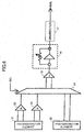
- FIG. 1 is a schematic diagram showing an optical disk apparatus.
- a spot of laser light is emitted on a medium 1, and reflection light is detected by a pickup 2.
- the reproducing signal detected is processed at a reproducing circuit 3.
- the data format of a user data component generated by the reproducing circuit 3 is converted by a decoder 4.
- the converted user data is delivered to an external host (illustration thereof is omitted) via a CPU 5.
- information to be recorded is delivered from the external host to an encoder 6 via the CPU 5.
- the data format of the information is converted by the encoder 6.
- the information is written on the medium 1 such that a laser controlling circuit 7 controls emission of the laser carried on the pickup 2 according to information bit.
- a push-pull signal (a kind of track error signal) detected by the pickup 2 is sent to a wobble detection circuit 8.
- a wobble signal extracted is sent to a servo circuit 9 or a clock generation circuit 10.
- the servo circuit 9 controls rotation of a motor 11 carrying the medium 1.
- the clock generation circuit 10 generates an accurate clock following rotation of the medium 1.
- the push-pull signal including the physical address is sent to an address detection circuit 12. Then, the push-pull signal is converted into address information by an address decoder 13.
- the address decoder 13 decodes the address information of accessing position.
- the pickup 2 carries an objective lens that focuses the laser light and a photodetector (light receiving) element that receives the reflection light from the medium 1.
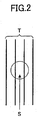
- FIG. 2 shows an enlarged view of a part of the medium, and tracks T and a spot S are shown.
- the push-pull signal is obtained by a difference between the reflection light in the right side and the reflection light in the left side with respect to a dividing line in a direction tangential to the track.
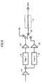
- FIG. 3A shows a divided-by-two photodectector (light receiving) element 100, which is divided into two photodetector parts A and B by a dividing line L1.
- the dividing line L1 is in a tangential direction to the track.
- FIG. 3B shows a subtracting amplifier reproducing the push-pull signal PPS.
- the push-pull signal PPS can be obtained by subtracting B from A using the subtracting amplifier shown in FIG. 3B.
- FIG. 4A shows a divided-by-four photodetector (light receiving) element 101 divided into four photodetector parts A, B, C and D by the dividing line L1 and a dividing line L2.
- the dividing line L2 is orthogonal to the track.
- the output signals of the photodetector parts A, B, C and D will respectively be denoted by A, B, C and D.
- FIG. 4B shows two adding amplifiers and a subtracting amplifier.
- the push-pull signal PPS can be obtained as follows: the adding amplifiers add A and B to D and C, respectively.
- the subtracting amplifier calculates a difference between the two calculated results, that is, (A + D) - (B + C). Accordingly, the wobble signals can be obtained from predetermined components included in the push-pull signals obtained as described above.
- FIG. 5 is a schematic diagram showing a first embodiment (corresponding to claim 1) of the present invention.
- a photodetector (light receiving) element is used in common for receiving the reflection light from the medium irrespective of the pre-format.
- a photodetector (light receiving) element 14 is the divided-by-four photodetector (light receiving) element.
- a and D, and B and C are symmetric with respect to the dividing line that is orthogonal to the track.
- Two adding amplifiers 15 add A and B to D and C, respectively, so as to generate two signals A + D and B + C.
- the two signals are divided by the dividing line in the tangential direction to the track.
- the photodetector (light receiving) element 14 may be the divided-by-two photodetector (light receiving) element or a structure of more parts as long as the two signals divided by the dividing line in the tangential direction to the track are generated.
- the push-pull signals are generated by calculating the difference between the two signals by a subtracting amplifier 16. Then, by digitalizing the push-pull signals by a binary circuit 17, binary wobble signals BWS are produced. Any one of the amplifiers in the process described above or an amplifier 18 inserted between the subtracting amplifier 16 and the binary circuit 17 may have a gain switching function so as to set an appropriate gain in accordance with the pre-format.
- the amplifier 18 is surrounded by a broken line so as to indicate that the adding amplifier 15 or the subtracting amplifier 16 may include the function of the amplifier 18. For, since the wobble signal strength standardized at the reproducing signal level differs depending on the pre-format, the appropriate gain for obtaining the binary wobble signals BWS of high quality differs depending on the pre-format.
- FIG. 6 is a schematic diagram showing a second embodiment (corresponding to claims 2 and 4) of the present invention.
- This embodiment shows the structure of the wobble signal detection circuit when the divided photodetector element receiving the reflection light from the medium differs depending on the pre-format. Further, in FIGS. 6 through 12, those elements that are the same as those corresponding elements in FIG. 5 are designated by the same reference numerals.
- FIGS. 6 through 8 two types of the pre-formats, a type A and a type B, are shown as examples. Additionally, in FIG. 6, it is assumed that a photodetector (light receiving) element 21 of the type A is a divided-by-four photodetector element, and a photodetector (light receiving) element 22 of the type B is a divided-by-two photodetector element. Thus, in order to make the circuit after the subtracting amplifier 16 the same as the circuit shown in FIG. 5, it is preferable to select signals before the subtracting amplifier 16.
- a signal processing of the type A pre-format is as follows: with regard to outputs of the photodetector element 21, each addition amplifier 23 adds a pair of the signals that are symmetric with respect to the dividing line; the dividing line is orthogonal to the track; two signals generated are divided by the dividing line in the tangential direction to the track.
- the outputs of the photodetector element 22 of the type B are directly input to a selector 24 since the photodetector element 22 is the divided-by-two photodetector element.
- the photodetector elements may alternately be structures with more blocks instead of the divided-by-two photodetector element or the divided-by-four photodetector element, as long as two signals divided by the dividing line in the tangential direction to the track are produced before the signals are sent to the selector 24.
- the pairs of signals obtained from a plurality of media having different pre-formats are input to the selector 24, and a pair of signals are selected by the pre-format selection signal SEL.
- the process thereafter is the same as the process of the circuit in FIG. 5.
- FIG. 7 shows a case where a plurality of photodetector (light receiving) elements 26 and 27 have parts of the same number.
- outputs of these photodetector elements 26 and 27 may directly be input to a selector 28. Then, the signals selected by the selector 28 may be added up by an adding amplifier 29.
- FIG. 8 shows a third embodiment (corresponding to claims 3 and 4) of the present invention.
- a type A wobble detection circuit W1 and a type B wobble detection circuit W2 a plurality of circuits are provided in parallel as many as the number of the photodetector elements.
- the circuits have the same structure as the circuit shown in FIG. 5 with regard to a part from the divided photodetector element 14 to the subtracting amplifier 16.
- a selector 30 selects an output from the outputs of the wobble detection circuits W1 and W2.
- the binary wobble signal is obtained by the binary circuit 17. Needless to say, it may be possible to provide a plurality of circuits including the structure from the detection circuit to the binary circuit 17 in parallel. However, it is preferable that the output is selected before the output is input to an output terminal so as not to increase the number of the output terminals when the circuit is incorporated in an LSI.
- the amplifiers 18 in FIGS. 6 through 8 surrounded by the broken lines have the gain switching function so as to set the gain suitable for the pre-formats (corresponding to claim 4).
- the adding amplifier or the subtracting amplifier may have the function mentioned above.
- the gain switching function is necessary for the amplifiers 18 in FIGS. 6 and 7 since the amplifiers 18 are provided between a plurality of detection circuits and a single binary circuit 17.
- the amplifier 18 may have a fixed amplification function suitable for a pre-format.
- FIG. 9 shows a fourth embodiment (corresponding to claim 5) of the present invention.
- the part before the subtracting amplifier 16 is the same as the corresponding part of the circuit mentioned above.
- the output of the subtracting amplifier 16, a push-pull signal passes through a filter circuit 19 for extracting the wobble signal component by eliminating a noise component.
- the push-pull signal is amplified to proper amplitude by an amplifier 20, and converted into a digital signal by the binary circuit 17.
- Sets of the filter circuit 19 and the amplifier 20 exclusive for corresponding pre-formats are provided in parallel as many as the number of the pre-formats, or sets of the filter circuit 19 and the amplifier 20 that serve for a plurality of pre-formats of the wobble signal frequencies that are approximately the same may also be provided.
- the set of the filter circuit 19 and the amplifier 20 serves for a plurality of pre-formats, the number of the photodetector elements and the number of the filters may be different.
- Outputs of the amplifiers 20 are sent to the selector 30.
- One of the outputs is selected by the selecting signal SEL corresponding to the pre-format.
- the selected output is input to the binary circuit 17.
- the filter circuit is provided after the selector 30.
- the selector 30 selects one of the outputs of the plurality of subtracting amplifiers. Then, the selected output is sent to the filter circuit.
- FIG. 10 shows a fifth embodiment (corresponding to claims 6 and 7) of the present invention.
- a filter circuit 21 extracts a wobble signal component from the push-pull signal output by the subtracting amplifier 16 by eliminating the noise component.
- the filter circuit 21 is a variable frequency characteristic filter that can be used in common for the pre-formats of different wobble signal frequencies.
- the variable frequency characteristic is such that a cut-off frequency of the filter changes according to a signal provided from outside of the circuit, a data channel clock signal, for example, or a frequency of a reference signal obtained by dividing a data channel clock signal by a 1/X frequency divider circuit 22.
- the filter circuit 21 As a general circuit, there are a SCF (switched capacitor filter) and a phase comparison filter. These filters can change the frequency characteristics almost continuously.
- providing the filter circuit 21 is equivalent to providing a plurality of filters that have different fixed frequency characteristics. Accordingly, providing the filter circuit 21 has the advantages of size and characteristics.
- the wobble signal frequency changes continuously depending on radius when rotating a medium at CAV (constant angular velocity) when the wobble is formed on the medium so as to realize the CLV (constant linear velocity).
- the wobble signal frequency becomes low at the inner diameter and high at the outer diameter. Accordingly, it is necessary to provide a multitude of filters, each of which has different fixed frequency characteristics, when accessing the medium of CLV format at CAV. However, it is preferable to use the filter of variable frequency characteristics since better continuity is secured.
- FIG. 11 shows a sixth embodiment (corresponding to claim 8) of the present invention.
- the circuit ahead of the binary circuit 17 is the same structure as the circuit mentioned above.
- the binary wobble signal BWS digitized by the binary circuit 17 passes through both an inversion buffer 40 that reverses the polarity and an-noninversion buffer 41 that does not change the polarity.
- the selector 30 selects one of outputs of the inversion buffer 40 and the noninversion buffer 41.
- the selector 30 makes a selection based on a polarity selection signal POL as a connection-switching signal.
- a structure may also be possible in which the polarity of the signal output by the subtraction amplifier is reversed though the illustration thereof is omitted.
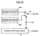
- FIG. 12 shows a seventh embodiment (corresponding to claim 9) of the present invention.
- a physical address is formed on a medium for recording so that an approximate position can be identified though in an unrecorded area.
- the physical address can be identified by frequency modulation to the wobble signals in CD, by prepits between tracks in DVD-RAM, and by LPP (land prepits) between tracks in DVD-R.
- LPP laand prepits
- the selector 30 switches address detection circuits (for example, an address detection circuit 33A for the type A pre-format and an address detection circuit 33B for the type B pre-format as shown in FIG. 12) so as to obtain an address signal ADS.
Abstract
Description
- The present invention relates to a circuit for detecting a wobble signal from various kinds of media having different pre-formats.
- A general recording medium employs a pre-format in which a wobble signal frequency detectable from deviation of tracks formed on the medium becomes constant when constant linear velocity (CLV) rotation control is performed in order to detect a linear velocity at a radial position accurately. A detailed description of the wobble signal will be given later.
- The wobble signal frequency differs depending on the pre-format. For example, CD, DVD-RAM, end DVD-R have different wobble signal frequencies. Additionally, physical address information is also necessary so as to identify an approximate position in an unrecorded area. However, the physical address information is obtained by different method depending on the pre-format. For example, the physical address information is obtained by performing frequency modulation to the wobble signals in a CD, by prepits in a DVD-RAM, and by land prepits formed between tracks in a DVD-R.
- A simple method to cope with a plurality of media having different pre-formats is to carry detection circuits exclusive for respective pre-formats in parallel and to select the detection circuit depending on the pre-format of the medium to be accessed.
- In Japanese Laid-Open Patent Application No. 2000-207745 "Wobble Clock Generating Circuit and Optical Disc Apparatus Using the Same", two or more filter circuits are provided so as to select the filter suitable for the wobble signal that changes frequency according to rotational errors of a spindle motor.
- As in the case of the above-mentioned publication, there is a case where a plurality of the filter circuits are carried in parallel even for one formatted medium and the suitable filter circuit is selected and used. A structure in the above-mentioned case is for preventing performance of the wobble signal detection from deteriorating due to change of rotational velocity of the medium.
- Thus, in an apparatus which records on and reproduces a plurality of the media having various pre-formats, when the wobble detection circuits exclusive for respective pre-formats are provided or when, as in the above publication, a plurality of filter circuits are carried in parallel for one pre-format medium, the circuit size becomes very large. Accordingly, power consumption increases and it becomes difficult to reduce the circuit size.
- It is a general object of the present invention to provide an improved and useful circuit structure in which the above-mentioned problems are eliminated.
- The object described above is achieved, according to one aspect of the present invention, by a wobble detection circuit, wherein: a signal is detected by a common photodetector (light receiving) element from several kinds of media having different pre-formats; and a gain for amplifying the signal in a wobble signal detection process is changed depending on the pre-format of a reproducing or recording media to obtain a wobble signal. Thus, a wobble signal of good quality can be detected since signal processing can be performed while maintaining suitable signal strength with regard to signals obtained by a plurality of media having different pre-formats and signal strength as well as different frequencies of signals.
- The object described above is also achieved, according to another aspect of the present invention, by a wobble detection circuit, wherein a plurality of divided photodetector (light receiving) elements are provided, each of the photodetector elements receives reflectional light from each corresponding medium among several kinds of media having different pre-formats, and a pair of outputs of the photodetector element are selected so as to share a rear processing circuit. Thus, many parts of the wobble detection circuit can be used in common irrespective of the pre-formats of the media, and power consumption can be reduced since the size of the wobble detection circuit is reduced. Additionally, the above-mentioned wobble detection circuit can be applied to an optical system having a divided structure for each photodetector element.
- The object described above is also achieved, according to another aspect of the present invention, by a wobble detection circuit, wherein a plurality of divided photodetector (light receiving) elements are provided, each of the photodetector elements receives reflectional light from each corresponding medium among several kinds of media having different pre-formats, and after obtaining push-pull signals from outputs of the photodetector elements, one of the push-pull signals is selected so as to use the rear processing circuit in common. Thus, a part of the wobble detection circuit can be used in common irrespective of the pre-formats of the media, and the power consumption can be reduced since the size of the circuit is reduced. Additionally, it is possible to obtain the wobble signals of good quality since the process up to the generation of a push-pull signal is performed before a selector, and homologous noise components superimposed on two signals input to a subtracting amplifier can be eliminated effectively.
- The object described above is also achieved, according to another aspect of the present invention, by the wobble detection circuit, wherein wobble signals of good quality can be obtained since a gain for amplifying the signal in a wobble signal detection process is changed depending on the pre-format so that signal processing is possible while maintaining suitable signal strength for the signals obtained by the plurality of media having different pre-formats as well as frequencies of the wobble signals.
- The object described above is also achieved, according to another aspect of the present invention, by the wobble detection circuit, wherein a plurality of filter circuits having variable frequency characteristics are provided, and the filter circuit is selected according to the wobble frequency to be detected. Thus, it is possible to obtain the wobble signals of good quality by providing an exclusive circuit for each wobble frequency with regard to an important part relating to performance of signal detection, while using a part of the circuit in common irrespective of the pre-formats of the media.
- The object described above is also achieved, according to another aspect of the present invention, by the wobble detection circuit, wherein the frequency characteristic of the filter circuit is changed according to the frequency to be detected. Thus, it is possible to detect a wobble signal with the single filter circuit from a multitude of media having different pre-formats. Additionally, the single filter circuit can be used in a CAV (constant angular velocity) access in which the wobble frequency is changed continuously.
- The object described above is also achieved, according to another aspect of the present invention, by the wobble detection circuit that can be used for pre-formats of various frequencies merely by setting a dividing ratio calculated by relationship between a channel clock signal and a wobble signal to a divider circuit, since a signal obtained by dividing the channel clock of reproducing or recording data by a variable divider circuit is used for a reference signal determining the frequency characteristic of the filter circuit.
- The object described above is also achieved, according to another aspect of the present invention, by the wobble detection circuit, wherein the polarity of the wobble signal is inverted depending on the pre-format of the media. Thus, it is possible to generate a binary wobble signal with a desired polarity irrespective of the given polarity of the wobble signal of each pre-format.
- The object described above is also achieved, according to another aspect of the present invention, by the wobble detection circuit, wherein characteristics of the wobble detection circuit are changed and a selection of a physical address detection circuit is made based on a selected signal depending on the pre-format. Thus, an operation of an unused address detection circuit can be stopped. At the same time, an output terminal of the address signal as well as a terminal of the wobble signal can be used in common when the wobble detection circuit is carried on such as an LSI, so that the size of a package can be reduced.
- The object described above is also achieved, according to another aspect of the present invention, by an optical disk apparatus that carries the wobble detection circuit and can record on or reproduce several 'kinds of the media having different pre-formats. Thus, it is possible to realize a small and power-saving optical disk apparatus having effective and high-performance circuit structure.
- Other objects, features and advantages of the present invention will become more apparent from the following detailed description when read in conjunction with the following drawings.
-
- FIG. 1 is a block diagram showing a general structure of an optical disk apparatus;
- FIG. 2 is an enlarged view of a part of a medium;
- FIGS. 3A is an illustrative drawing showing a divided-by-two photodetector (light receiving) element;
- FIG. 3B is an illustrative drawing showing a subtracting amplifier producing a push-pull signal;
- FIG. 4A is an illustrative drawing showing a divided-by-four photodetector (light receiving) element;
- FIG. 4B is an illustrative drawing showing adding amplifiers and a subtracting amplifier producing a push-pull signal;
- FIG. 5 is a block diagram showing a first embodiment of the present invention;
- FIG. 6 is a block diagram showing a second embodiment of the present invention;
- FIG. 7 is a block diagram showing a second embodiment of the present invention;
- FIG. 8 is a block diagram showing a third embodiment of the present invention;
- FIG. 9 is a block diagram showing a fourth embodiment of the present invention;
- FIG. 10 is a block diagram showing a fifth embodiment of the present invention;
- FIG. 11 is a block diagram showing a sixth embodiment of the present invention; and
- FIG. 12 is a block diagram showing a seventh embodiment of the present invention.
-
- FIG. 1 is a schematic diagram showing an optical disk apparatus. A spot of laser light is emitted on a
medium 1, and reflection light is detected by apickup 2. The reproducing signal detected is processed at a reproducingcircuit 3. The data format of a user data component generated by the reproducingcircuit 3 is converted by adecoder 4. The converted user data is delivered to an external host (illustration thereof is omitted) via aCPU 5. - Additionally, information to be recorded is delivered from the external host to an
encoder 6 via theCPU 5. The data format of the information is converted by theencoder 6. Then, the information is written on the medium 1 such that a laser controlling circuit 7 controls emission of the laser carried on thepickup 2 according to information bit. - On the other hand, a push-pull signal (a kind of track error signal) detected by the
pickup 2 is sent to awobble detection circuit 8. A wobble signal extracted is sent to aservo circuit 9 or aclock generation circuit 10. Theservo circuit 9 controls rotation of amotor 11 carrying themedium 1. Theclock generation circuit 10 generates an accurate clock following rotation of themedium 1. - Additionally, the push-pull signal including the physical address is sent to an
address detection circuit 12. Then, the push-pull signal is converted into address information by anaddress decoder 13. Theaddress decoder 13 decodes the address information of accessing position. Thepickup 2 carries an objective lens that focuses the laser light and a photodetector (light receiving) element that receives the reflection light from themedium 1. - The simplest example of a generation method of the wobble signal used in the present invention is to detect the wobble signal from the push-pull signal. FIG. 2 shows an enlarged view of a part of the medium, and tracks T and a spot S are shown. The push-pull signal is obtained by a difference between the reflection light in the right side and the reflection light in the left side with respect to a dividing line in a direction tangential to the track. FIG. 3A shows a divided-by-two photodectector (light receiving)
element 100, which is divided into two photodetector parts A and B by a dividing line L1. The dividing line L1 is in a tangential direction to the track. Output signals of the photodetector parts A and B will respectively be denoted by A and B. FIG. 3B shows a subtracting amplifier reproducing the push-pull signal PPS. When the divided-by-two photodetector element is used, the push-pull signal PPS can be obtained by subtracting B from A using the subtracting amplifier shown in FIG. 3B. - FIG. 4A shows a divided-by-four photodetector (light receiving)
element 101 divided into four photodetector parts A, B, C and D by the dividing line L1 and a dividing line L2. The dividing line L2 is orthogonal to the track. The output signals of the photodetector parts A, B, C and D will respectively be denoted by A, B, C and D. FIG. 4B shows two adding amplifiers and a subtracting amplifier. When the divided-by-four photodetector element is used, the push-pull signal PPS can be obtained as follows: the adding amplifiers add A and B to D and C, respectively. Then, the subtracting amplifier calculates a difference between the two calculated results, that is, (A + D) - (B + C). Accordingly, the wobble signals can be obtained from predetermined components included in the push-pull signals obtained as described above. - A description will be given of the wobble detection circuit of the present invention.
- FIG. 5 is a schematic diagram showing a first embodiment (corresponding to claim 1) of the present invention. In this embodiment, a photodetector (light receiving) element is used in common for receiving the reflection light from the medium irrespective of the pre-format.
- It is assumed that a photodetector (light receiving)
element 14 is the divided-by-four photodetector (light receiving) element. A and D, and B and C are symmetric with respect to the dividing line that is orthogonal to the track. Two addingamplifiers 15 add A and B to D and C, respectively, so as to generate two signals A + D and B + C. The two signals are divided by the dividing line in the tangential direction to the track. Needless to say, the photodetector (light receiving)element 14 may be the divided-by-two photodetector (light receiving) element or a structure of more parts as long as the two signals divided by the dividing line in the tangential direction to the track are generated. - The push-pull signals are generated by calculating the difference between the two signals by a subtracting
amplifier 16. Then, by digitalizing the push-pull signals by abinary circuit 17, binary wobble signals BWS are produced. Any one of the amplifiers in the process described above or anamplifier 18 inserted between the subtractingamplifier 16 and thebinary circuit 17 may have a gain switching function so as to set an appropriate gain in accordance with the pre-format. - The
amplifier 18 is surrounded by a broken line so as to indicate that the addingamplifier 15 or the subtractingamplifier 16 may include the function of theamplifier 18. For, since the wobble signal strength standardized at the reproducing signal level differs depending on the pre-format, the appropriate gain for obtaining the binary wobble signals BWS of high quality differs depending on the pre-format. - FIG. 6 is a schematic diagram showing a second embodiment (corresponding to
claims 2 and 4) of the present invention. This embodiment shows the structure of the wobble signal detection circuit when the divided photodetector element receiving the reflection light from the medium differs depending on the pre-format. Further, in FIGS. 6 through 12, those elements that are the same as those corresponding elements in FIG. 5 are designated by the same reference numerals. - In FIGS. 6 through 8, two types of the pre-formats, a type A and a type B, are shown as examples. Additionally, in FIG. 6, it is assumed that a photodetector (light receiving)
element 21 of the type A is a divided-by-four photodetector element, and a photodetector (light receiving)element 22 of the type B is a divided-by-two photodetector element. Thus, in order to make the circuit after the subtractingamplifier 16 the same as the circuit shown in FIG. 5, it is preferable to select signals before the subtractingamplifier 16. - That is, a signal processing of the type A pre-format is as follows: with regard to outputs of the
photodetector element 21, eachaddition amplifier 23 adds a pair of the signals that are symmetric with respect to the dividing line; the dividing line is orthogonal to the track; two signals generated are divided by the dividing line in the tangential direction to the track. The outputs of thephotodetector element 22 of the type B are directly input to aselector 24 since thephotodetector element 22 is the divided-by-two photodetector element. Needless to say, the photodetector elements may alternately be structures with more blocks instead of the divided-by-two photodetector element or the divided-by-four photodetector element, as long as two signals divided by the dividing line in the tangential direction to the track are produced before the signals are sent to theselector 24. The pairs of signals obtained from a plurality of media having different pre-formats are input to theselector 24, and a pair of signals are selected by the pre-format selection signal SEL. The process thereafter is the same as the process of the circuit in FIG. 5. - FIG. 7 shows a case where a plurality of photodetector (light receiving)
elements photodetector elements selector 28. Then, the signals selected by theselector 28 may be added up by an addingamplifier 29. - FIG. 8 shows a third embodiment (corresponding to
claims 3 and 4) of the present invention. - As shown by a type A wobble detection circuit W1 and a type B wobble detection circuit W2, a plurality of circuits are provided in parallel as many as the number of the photodetector elements. The circuits have the same structure as the circuit shown in FIG. 5 with regard to a part from the divided
photodetector element 14 to the subtractingamplifier 16. Aselector 30 selects an output from the outputs of the wobble detection circuits W1 and W2. The binary wobble signal is obtained by thebinary circuit 17. Needless to say, it may be possible to provide a plurality of circuits including the structure from the detection circuit to thebinary circuit 17 in parallel. However, it is preferable that the output is selected before the output is input to an output terminal so as not to increase the number of the output terminals when the circuit is incorporated in an LSI. - The same as the amplifier shown in FIG. 5, the
amplifiers 18 in FIGS. 6 through 8 surrounded by the broken lines have the gain switching function so as to set the gain suitable for the pre-formats (corresponding to claim 4). Needless to say, the adding amplifier or the subtracting amplifier may have the function mentioned above. Especially, the gain switching function is necessary for theamplifiers 18 in FIGS. 6 and 7 since theamplifiers 18 are provided between a plurality of detection circuits and a singlebinary circuit 17. On the other hand, when theamplifier 18 is provided for each detection circuit, theamplifier 18 may have a fixed amplification function suitable for a pre-format. - FIG. 9 shows a fourth embodiment (corresponding to claim 5) of the present invention.
- The part before the subtracting
amplifier 16 is the same as the corresponding part of the circuit mentioned above. The output of the subtractingamplifier 16, a push-pull signal, passes through afilter circuit 19 for extracting the wobble signal component by eliminating a noise component. Then, the push-pull signal is amplified to proper amplitude by anamplifier 20, and converted into a digital signal by thebinary circuit 17. Sets of thefilter circuit 19 and theamplifier 20 exclusive for corresponding pre-formats are provided in parallel as many as the number of the pre-formats, or sets of thefilter circuit 19 and theamplifier 20 that serve for a plurality of pre-formats of the wobble signal frequencies that are approximately the same may also be provided. When the set of thefilter circuit 19 and theamplifier 20 serves for a plurality of pre-formats, the number of the photodetector elements and the number of the filters may be different. - Outputs of the
amplifiers 20 are sent to theselector 30. One of the outputs is selected by the selecting signal SEL corresponding to the pre-format. The selected output is input to thebinary circuit 17. The above explanation is given on the assumption that the subtractingamplifier 16 receives outputs from a plurality of adding amplifiers. Needless to say, it may be possible to employ a structure in which the filter circuit is provided after theselector 30. In this structure, theselector 30 selects one of the outputs of the plurality of subtracting amplifiers. Then, the selected output is sent to the filter circuit. - FIG. 10 shows a fifth embodiment (corresponding to
claims 6 and 7) of the present invention. - A
filter circuit 21 extracts a wobble signal component from the push-pull signal output by the subtractingamplifier 16 by eliminating the noise component. Thefilter circuit 21 is a variable frequency characteristic filter that can be used in common for the pre-formats of different wobble signal frequencies. The variable frequency characteristic is such that a cut-off frequency of the filter changes according to a signal provided from outside of the circuit, a data channel clock signal, for example, or a frequency of a reference signal obtained by dividing a data channel clock signal by a 1/Xfrequency divider circuit 22. - As a general circuit, there are a SCF (switched capacitor filter) and a phase comparison filter. These filters can change the frequency characteristics almost continuously. Thus, providing the
filter circuit 21 is equivalent to providing a plurality of filters that have different fixed frequency characteristics. Accordingly, providing thefilter circuit 21 has the advantages of size and characteristics. For example, the wobble signal frequency changes continuously depending on radius when rotating a medium at CAV (constant angular velocity) when the wobble is formed on the medium so as to realize the CLV (constant linear velocity). The wobble signal frequency becomes low at the inner diameter and high at the outer diameter. Accordingly, it is necessary to provide a multitude of filters, each of which has different fixed frequency characteristics, when accessing the medium of CLV format at CAV. However, it is preferable to use the filter of variable frequency characteristics since better continuity is secured. - FIG. 11 shows a sixth embodiment (corresponding to claim 8) of the present invention.
- In an example shown in FIG. 11, the circuit ahead of the
binary circuit 17 is the same structure as the circuit mentioned above. The binary wobble signal BWS digitized by thebinary circuit 17 passes through both aninversion buffer 40 that reverses the polarity and an-noninversion buffer 41 that does not change the polarity. Then, theselector 30 selects one of outputs of theinversion buffer 40 and thenoninversion buffer 41. Theselector 30 makes a selection based on a polarity selection signal POL as a connection-switching signal. A structure may also be possible in which the polarity of the signal output by the subtraction amplifier is reversed though the illustration thereof is omitted. - FIG. 12 shows a seventh embodiment (corresponding to claim 9) of the present invention.
- A physical address is formed on a medium for recording so that an approximate position can be identified though in an unrecorded area. For example, the physical address can be identified by frequency modulation to the wobble signals in CD, by prepits between tracks in DVD-RAM, and by LPP (land prepits) between tracks in DVD-R. When the pre-format differs in this way, a physical address detection circuit as well as the wobble signal frequency differ. Thus, by using selection signal SEL that selects the
wobble detection circuit 32 depending on the pre-format, theselector 30 switches address detection circuits (for example, anaddress detection circuit 33A for the type A pre-format and anaddress detection circuit 33B for the type B pre-format as shown in FIG. 12) so as to obtain an address signal ADS. - As mentioned above, when a plurality of media with different pre-formats use the same detection circuits of the wobble signal and the address signal in common, not only the size of the circuit can be reduced but also an output terminal can be used in common so as to use a small size package.
- The present invention is not limited to the specifically disclosed embodiments, and variations and modifications may be made without departing from the scope of the present invention.
- The present application is based on Japanese priority application No. 2001-081152 filed on March 21, 2001, the entire contents of which are hereby incorporated by reference.
Claims (9)
- A wobble detection circuit detecting a wobble signal from an output of a common photodetector element for several kinds of recording or reproducing media having different pre-formats, characterized by comprising:a plurality of filter circuits extracting a wobble signal by removing a noise component from the output of said photodetector element, said filter circuits each corresponding to one of the pre-formats of the media.
- A wobble detection circuit detecting a wobble signal from an output of a common photodetector element for several kinds of recording or reproducing media having different pre-formats, characterized by comprising:a filter circuit having a variable frequency characteristic that is varied according to a wobble frequency to be detected.
- The wobble detection circuit as claimed in claim 2, characterized by further comprising:wherein an output of said divider circuit is used as a reference signal of the filter circuit and supplied to the filter circuit,a divider circuit dividing a channel clock signal that is a basis for reproducing or recording data,
the frequency characteristic of the filter circuit is determined by a frequency of the reference signal supplied from said divider circuit, and
the frequency characteristic of the filter circuit is varied by changing a dividing ratio of said divider circuit. - The wobble detection circuit as claimed in claim 2 or 3, wherein the filter circuit is constructed by one of a switched capacitor filter and a phase comparison filter.
- The wobble detection circuit as claimed in any of claims 2-4, wherein, when accessing at a constant angular velocity a medium on which a wobble is carved such that a linear velocity becomes constant, the wobble signal is detected by using the filter circuit.
- The wobble detection circuit as claimed in any of claims 1-5, characterized by further comprising:wherein the polarity is selected according to a pre-format of a reproducing or recording medium.an inversion circuit inverting polarity of the wobble signal; anda selector selecting one of noninversion and inversion,
- The wobble detection circuit as claimed in claim 6, characterized by further comprising:wherein a characteristic of the wobble detection circuit is varied and one of said physical address detection circuits is selected based on a selecting signal according to the pre-format of the reproducing or recording medium.a plurality of physical address detection circuits each corresponding to one of the pre-formats of the reproducing or recording media; anda selector selecting one of said physical address detection circuits,
- An optical disk apparatus performing recording or reproducing with regard to several kinds of media having different pre-formats, said optical disk apparatus characterized by comprising:a wobble detection circuit detecting a wobble signal from an output of a common photodetector element for the several kinds of media, said wobble detection circuit comprising:a plurality of filter circuits extracting a wobble signal by removing a noise component from the output of said photodetector element, said filter circuits each corresponding to one of the pre-formats of the media.
- An optical disk apparatus performing recording or reproducing with regard to several kinds of media having different pre-formats, said optical disk apparatus characterized by comprising:a wobble detection circuit detecting a wobble signal from an output of a common photodetector element for the several kinds of media, comprising:a filter circuit having a variable frequency characteristic that is varied according to a wobble frequency to be detected.
Applications Claiming Priority (3)
| Application Number | Priority Date | Filing Date | Title |
|---|---|---|---|
| JP2001081152 | 2001-03-21 | ||
| JP2001081152A JP2002279640A (en) | 2001-03-21 | 2001-03-21 | Wobble detecting circuit and device thereof |
| EP02251986A EP1244099B1 (en) | 2001-03-21 | 2002-03-20 | Wobble detection circuit and optical disk apparatus |
Related Parent Applications (1)
| Application Number | Title | Priority Date | Filing Date |
|---|---|---|---|
| EP02251986A Division EP1244099B1 (en) | 2001-03-21 | 2002-03-20 | Wobble detection circuit and optical disk apparatus |
Publications (3)
| Publication Number | Publication Date |
|---|---|
| EP1376552A2 true EP1376552A2 (en) | 2004-01-02 |
| EP1376552A3 EP1376552A3 (en) | 2004-02-04 |
| EP1376552B1 EP1376552B1 (en) | 2006-03-15 |
Family
ID=18937306
Family Applications (2)
| Application Number | Title | Priority Date | Filing Date |
|---|---|---|---|
| EP02251986A Expired - Lifetime EP1244099B1 (en) | 2001-03-21 | 2002-03-20 | Wobble detection circuit and optical disk apparatus |
| EP03077803A Expired - Lifetime EP1376552B1 (en) | 2001-03-21 | 2002-03-20 | Wobble detection circuit and optical disk apparatus |
Family Applications Before (1)
| Application Number | Title | Priority Date | Filing Date |
|---|---|---|---|
| EP02251986A Expired - Lifetime EP1244099B1 (en) | 2001-03-21 | 2002-03-20 | Wobble detection circuit and optical disk apparatus |
Country Status (5)
| Country | Link |
|---|---|
| US (2) | US6888783B2 (en) |
| EP (2) | EP1244099B1 (en) |
| JP (1) | JP2002279640A (en) |
| DE (2) | DE60209946T2 (en) |
| ES (2) | ES2286205T3 (en) |
Families Citing this family (14)
| Publication number | Priority date | Publication date | Assignee | Title |
|---|---|---|---|---|
| JP4300727B2 (en) * | 2001-10-09 | 2009-07-22 | ソニー株式会社 | DISC RECORDING MEDIUM, DISC DRIVE DEVICE, REPRODUCTION METHOD, AND DISC MANUFACTURING METHOD |
| JP3566690B2 (en) | 2001-12-07 | 2004-09-15 | 株式会社リコー | Wobble signal detection circuit and optical disk device |
| EP1388850A1 (en) * | 2002-08-06 | 2004-02-11 | Deutsche Thomson-Brandt GmbH | Method for detecting a wobble signal |
| US7474603B2 (en) * | 2002-09-04 | 2009-01-06 | Ricoh Company, Ltd. | Optical information recording method, apparatus, and medium, laser control circuit, wobble signal detection method, and servo signal detection method |
| JP2004342158A (en) * | 2003-05-13 | 2004-12-02 | Pioneer Electronic Corp | Recording medium discriminating device, information reproducing device, and information recording device |
| EP1662488A1 (en) | 2003-09-02 | 2006-05-31 | Ricoh Company, Ltd. | Push-pull signal generation device and optical disc device |
| US7317667B2 (en) * | 2003-10-31 | 2008-01-08 | Matsushita Electric Industrial Co., Ltd. | Wobble signal extraction circuit and optical disk device |
| US7706242B2 (en) * | 2004-02-25 | 2010-04-27 | Ricoh Company, Ltd. | Optical disk, signal generation method, clock signal generation method, and optical disk device |
| US7633846B2 (en) * | 2004-03-15 | 2009-12-15 | Ricoh Company, Ltd. | Multi-level information reproducing method, multi-level information recording medium, multi-level information waveform equalizing device, multi-level information reproducing apparatus, multi-level information recording apparatus, signal processing method, reproduced signal processing circuit and optical disk apparatus |
| JP4247261B2 (en) | 2006-09-28 | 2009-04-02 | 東芝サムスン ストレージ・テクノロジー株式会社 | Optical disk device |
| JP2009129520A (en) * | 2007-11-26 | 2009-06-11 | Taiyo Yuden Co Ltd | Optical information recording medium, method of recording optical information therein, and optical information recorder |
| US20100329088A1 (en) * | 2008-02-06 | 2010-12-30 | Kinji Kayanuma | Device for determining existence of wobble, medium discrimination device, method of determining existence of wobble, and medium discrimination method |
| TW200942243A (en) | 2008-03-05 | 2009-10-16 | Biocryst Pharm Inc | Antiviral therapeutic agents |
| US8436504B2 (en) * | 2010-01-11 | 2013-05-07 | Ford Global Technologies, Llc | Stator for an electric machine |
Citations (6)
| Publication number | Priority date | Publication date | Assignee | Title |
|---|---|---|---|---|
| EP0753845A1 (en) * | 1995-01-31 | 1997-01-15 | Sony Corporation | Device for reproducing optical recording medium |
| JPH1064166A (en) * | 1996-08-15 | 1998-03-06 | Toshiba Corp | Disk reproducing device |
| EP0874356A2 (en) * | 1997-04-25 | 1998-10-28 | Pioneer Electronic Corporation | Optical disc discriminating system |
| EP0938084A2 (en) * | 1998-02-24 | 1999-08-25 | Sony Corporation | Reproduction apparatus and reproduction method |
| JP2000231726A (en) * | 1999-02-10 | 2000-08-22 | Hitachi Ltd | Optical disk reproducing device |
| US6172956B1 (en) * | 1996-01-26 | 2001-01-09 | Sharp Kabushiki Kaisha | Optical recording medium and optical recording/reproducing device, and manufacturing method of optical recording medium |
Family Cites Families (40)
| Publication number | Priority date | Publication date | Assignee | Title |
|---|---|---|---|---|
| US4879707A (en) * | 1985-07-30 | 1989-11-07 | Laser Magnetic Storage International Company | Optical disk tracking and seeking systems specific track formats using discontinuities |
| US5166921A (en) * | 1987-06-17 | 1992-11-24 | Pioneer Electronic Corporation | Optical disk carrying tracking information in multiple formats and apparatus for analyzing same |
| JPH0724142B2 (en) * | 1989-04-28 | 1995-03-15 | 株式会社ケンウッド | Optical disc servo circuit |
| JP3461017B2 (en) * | 1993-10-29 | 2003-10-27 | 株式会社ケンウッド | Spindle control circuit for optical disk drive |
| JP2860229B2 (en) * | 1993-06-25 | 1999-02-24 | 株式会社ケンウッド | Optical disk recording and playback device |
| JPH07169078A (en) | 1993-12-16 | 1995-07-04 | Sony Corp | Method for detecting wobble signal |
| JPH08185664A (en) | 1994-12-28 | 1996-07-16 | Kenwood Corp | Wobble detecting circuit for optical disk device |
| JP3458502B2 (en) | 1995-01-11 | 2003-10-20 | ソニー株式会社 | Optical disk drive |
| JP3410869B2 (en) | 1995-04-11 | 2003-05-26 | 株式会社リコー | Optical pickup device |
| JP3052994B2 (en) | 1995-06-30 | 2000-06-19 | ティアック株式会社 | Wobble signal detection circuit of optical disk device |
| JPH09198779A (en) | 1996-01-18 | 1997-07-31 | Pioneer Electron Corp | Disk discriminating device |
| KR100208714B1 (en) * | 1996-06-14 | 1999-07-15 | 윤종용 | Reproducing system for optical disc of a different kind |
| JP3671572B2 (en) * | 1997-01-10 | 2005-07-13 | ソニー株式会社 | Optical disk device |
| TW451191B (en) | 1997-03-19 | 2001-08-21 | Hitachi Ltd | Wobble signal detecting circuit, wobble abnormality detecting circuit, information processing apparatus using these circuit and method, and recording medium used in the apparatus or method |
| JP3653923B2 (en) | 1997-03-19 | 2005-06-02 | ソニー株式会社 | Recording / reproducing apparatus and method |
| JPH1166578A (en) | 1997-08-07 | 1999-03-09 | Sanyo Electric Co Ltd | Circuit for detecting wobble signal of disk player |
| KR100298929B1 (en) * | 1997-08-16 | 2001-10-26 | 구자홍 | Information recording/reproducing method and device |
| JPH1166602A (en) | 1997-08-25 | 1999-03-09 | Sanyo Electric Co Ltd | Optical pickup device and disk recording and reproducing device utilizing the same |
| KR100285315B1 (en) * | 1997-09-24 | 2001-04-02 | 구자홍 | Method and device for inspecting quality of optical disc |
| JPH11161982A (en) | 1997-09-25 | 1999-06-18 | Ricoh Co Ltd | Optical disk driving device and incidental information detecting circuit |
| DE19807809A1 (en) | 1998-02-26 | 1999-09-02 | Thomson Brandt Gmbh | Device for reading and / or writing to optical recording media |
| US6657929B1 (en) * | 1998-06-23 | 2003-12-02 | Matsushita Electric Industrial Co., Ltd. | Optical disk recording apparatus and method for recording data on optical disk |
| US6487149B1 (en) | 1998-10-09 | 2002-11-26 | Ricoh Company, Ltd. | Optical recording and reproducing methods for optical disk |
| JP2000207745A (en) | 1999-01-12 | 2000-07-28 | Hitachi Ltd | Wobble clock generating circuit and optical disc apparatus usint the same |
| JP2000285455A (en) | 1999-03-31 | 2000-10-13 | Ricoh Co Ltd | Wobble signal detection device and information recording device |
| JP2001093147A (en) | 1999-09-20 | 2001-04-06 | Teac Corp | Wobble signal detecting circuit of optical disk device |
| EP1098302A3 (en) * | 1999-11-03 | 2007-12-12 | SAMSUNG ELECTRONICS Co. Ltd. | Physical identification data addressing method using wobble signal, wobble address encoding circuit, method and circuit for detecting wobble address, and recording medium |
| JP2001134943A (en) | 1999-11-05 | 2001-05-18 | Yamaha Corp | Push-pull signal processing circuit, wobble extracting circuit and prepit detecting circuit, in optical disk recorder |
| JP4277452B2 (en) * | 2000-02-25 | 2009-06-10 | ソニー株式会社 | Recording device, playback device |
| JP4422855B2 (en) | 2000-03-16 | 2010-02-24 | 株式会社日立製作所 | Wobble signal regeneration circuit |
| JP4012673B2 (en) | 2000-08-23 | 2007-11-21 | パイオニア株式会社 | Wobble detector |
| JP2002074674A (en) | 2000-09-04 | 2002-03-15 | Matsushita Electric Ind Co Ltd | Wobble signal detecting circuit |
| KR100754160B1 (en) | 2001-06-30 | 2007-09-03 | 삼성전자주식회사 | Optical disc drive and method for reproducing wobble signal |
| JP2003030878A (en) | 2001-07-13 | 2003-01-31 | Sanyo Electric Co Ltd | Wobble signal detection circuit for optical disk recording and reproducing device |
| JP3890934B2 (en) | 2001-08-10 | 2007-03-07 | 日本ビクター株式会社 | Wobble signal detector |
| JP3914018B2 (en) | 2001-09-26 | 2007-05-16 | 株式会社リコー | Wobble signal detecting device and optical information recording / reproducing device |
| JP4121264B2 (en) | 2001-10-16 | 2008-07-23 | コーニンクレッカ フィリップス エレクトロニクス エヌ ヴィ | Disk drive device and wobble information detection method |
| US6809997B2 (en) | 2001-11-17 | 2004-10-26 | Lg Electronics Inc. | Apparatus and method for detecting wobble signal read from optical disc |
| JP3789423B2 (en) | 2001-11-17 | 2006-06-21 | エルジー電子株式会社 | Apparatus and method for encoding wobble signal recorded on optical disk, and apparatus and method for decoding wobble signal read from optical disk |
| JP3566690B2 (en) | 2001-12-07 | 2004-09-15 | 株式会社リコー | Wobble signal detection circuit and optical disk device |
-
2001
- 2001-03-21 JP JP2001081152A patent/JP2002279640A/en active Pending
-
2002
- 2002-03-20 DE DE60209946T patent/DE60209946T2/en not_active Expired - Lifetime
- 2002-03-20 EP EP02251986A patent/EP1244099B1/en not_active Expired - Lifetime
- 2002-03-20 ES ES02251986T patent/ES2286205T3/en not_active Expired - Lifetime
- 2002-03-20 US US10/101,201 patent/US6888783B2/en not_active Expired - Lifetime
- 2002-03-20 DE DE60220208T patent/DE60220208T2/en not_active Expired - Lifetime
- 2002-03-20 ES ES03077803T patent/ES2259749T3/en not_active Expired - Lifetime
- 2002-03-20 EP EP03077803A patent/EP1376552B1/en not_active Expired - Lifetime
-
2003
- 2003-08-15 US US10/641,078 patent/US7046615B2/en not_active Expired - Lifetime
Patent Citations (6)
| Publication number | Priority date | Publication date | Assignee | Title |
|---|---|---|---|---|
| EP0753845A1 (en) * | 1995-01-31 | 1997-01-15 | Sony Corporation | Device for reproducing optical recording medium |
| US6172956B1 (en) * | 1996-01-26 | 2001-01-09 | Sharp Kabushiki Kaisha | Optical recording medium and optical recording/reproducing device, and manufacturing method of optical recording medium |
| JPH1064166A (en) * | 1996-08-15 | 1998-03-06 | Toshiba Corp | Disk reproducing device |
| EP0874356A2 (en) * | 1997-04-25 | 1998-10-28 | Pioneer Electronic Corporation | Optical disc discriminating system |
| EP0938084A2 (en) * | 1998-02-24 | 1999-08-25 | Sony Corporation | Reproduction apparatus and reproduction method |
| JP2000231726A (en) * | 1999-02-10 | 2000-08-22 | Hitachi Ltd | Optical disk reproducing device |
Non-Patent Citations (3)
| Title |
|---|
| DATABASE WPI Section EI, Week 199904 Derwent Publications Ltd., London, GB; Class T03, AN 1999-042538 XP002264073 & KR 98 004 670 A (SAMSUNG ELECTRONICS CO LTD), 30 March 1998 (1998-03-30) * |
| PATENT ABSTRACTS OF JAPAN vol. 1998, no. 08, 30 June 1998 (1998-06-30) -& JP 10 064166 A (TOSHIBA CORP), 6 March 1998 (1998-03-06) * |
| PATENT ABSTRACTS OF JAPAN vol. 2000, no. 11, 3 January 2001 (2001-01-03) -& JP 2000 231726 A (HITACHI LTD), 22 August 2000 (2000-08-22) * |
Also Published As
| Publication number | Publication date |
|---|---|
| EP1244099B1 (en) | 2007-05-23 |
| EP1244099A3 (en) | 2004-09-22 |
| US7046615B2 (en) | 2006-05-16 |
| ES2259749T3 (en) | 2006-10-16 |
| EP1376552B1 (en) | 2006-03-15 |
| DE60209946D1 (en) | 2006-05-11 |
| DE60209946T2 (en) | 2006-12-28 |
| DE60220208T2 (en) | 2008-01-17 |
| US20040013063A1 (en) | 2004-01-22 |
| US6888783B2 (en) | 2005-05-03 |
| ES2286205T3 (en) | 2007-12-01 |
| EP1376552A3 (en) | 2004-02-04 |
| JP2002279640A (en) | 2002-09-27 |
| EP1244099A2 (en) | 2002-09-25 |
| DE60220208D1 (en) | 2007-07-05 |
| US20020136126A1 (en) | 2002-09-26 |
Similar Documents
| Publication | Publication Date | Title |
|---|---|---|
| US7046615B2 (en) | Wobble detection circuit corresponding to a plurality of media having different pre-formats and optical disk apparatus having reduced size | |
| US6466533B2 (en) | Prepit detection unit | |
| US6859425B2 (en) | Wobble signal detection circuit and optical disk device | |
| EP1067524A2 (en) | Pre-pit detector of optical recording medium | |
| JPH0773470A (en) | Draw type optical disk and its recorder | |
| JP2005196846A (en) | Wobble signal obtaining circuit and optical disk drive | |
| US7561503B2 (en) | Clock signal generating device and an optical disc apparatus incorporating the device | |
| JP2004039213A (en) | Mirror signal detection circuit and its method for optical disk drive | |
| JP2005353153A (en) | Phase difference detection circuit and optical disk device having the phase difference detection circuit | |
| US7529173B2 (en) | Optical disc device, circuit for optical disc device, wobble signal reproduction method, and land pre-pit signal reproduction method | |
| JP2000030263A (en) | Optical recording medium reader | |
| US20070217317A1 (en) | Optical disk device, playback method of the optical disk device, and reproduction signal generating circuit | |
| US6894956B2 (en) | Multimode filter | |
| US20070014203A1 (en) | Apparatus and method for detecting wobble signal in disc drive using phase control | |
| JP2004006002A (en) | Wobble detecting circuit and device thereof | |
| WO2005101388A1 (en) | Optical disc recording/reproduction device | |
| JP2004030858A (en) | Detecting apparatus, detecting method, and optical disk apparatus | |
| US8542564B2 (en) | Method for designating disk recording capacity and apparatus therefor | |
| US20040105362A1 (en) | Disk device and risk processing method | |
| JP2005353195A (en) | Wobble signal detector circuit and optical disk device | |
| JP2002197649A (en) | Signal detecting circuit | |
| JPWO2005043516A1 (en) | Wobble signal extraction circuit and optical disk apparatus | |
| US20050207309A1 (en) | Optical data reading device and optical data writing device, and information detecting method and information detecting circuit used in the same reading and/or writing devices | |
| JPH0696451A (en) | Device for driving magneto-optical medium | |
| JP2006012308A (en) | Optical disk device |
Legal Events
| Date | Code | Title | Description |
|---|---|---|---|
| PUAI | Public reference made under article 153(3) epc to a published international application that has entered the european phase |
Free format text: ORIGINAL CODE: 0009012 |
|
| PUAL | Search report despatched |
Free format text: ORIGINAL CODE: 0009013 |
|
| 17P | Request for examination filed |
Effective date: 20030916 |
|
| AC | Divisional application: reference to earlier application |
Ref document number: 1244099 Country of ref document: EP Kind code of ref document: P |
|
| AK | Designated contracting states |
Kind code of ref document: A2 Designated state(s): AT BE CH CY DE DK ES FI FR GB GR IE IT LI LU MC NL PT SE TR |
|
| AX | Request for extension of the european patent |
Extension state: AL LT LV MK |
|
| RIC1 | Information provided on ipc code assigned before grant |
Ipc: 7G 11B 7/09 B Ipc: 7G 11B 7/005 A |
|
| AK | Designated contracting states |
Kind code of ref document: A3 Designated state(s): AT BE CH CY DE DK ES FI FR GB GR IE IT LI LU MC NL PT SE TR |
|
| AX | Request for extension of the european patent |
Extension state: AL LT LV MK |
|
| AKX | Designation fees paid |
Designated state(s): DE ES FR GB IT NL |
|
| 17Q | First examination report despatched |
Effective date: 20041103 |
|
| 18W | Application withdrawn |
Effective date: 20041125 |
|
| D18W | Application withdrawn (deleted) | ||
| GRAP | Despatch of communication of intention to grant a patent |
Free format text: ORIGINAL CODE: EPIDOSNIGR1 |
|
| GRAS | Grant fee paid |
Free format text: ORIGINAL CODE: EPIDOSNIGR3 |
|
| GRAA | (expected) grant |
Free format text: ORIGINAL CODE: 0009210 |
|
| AC | Divisional application: reference to earlier application |
Ref document number: 1244099 Country of ref document: EP Kind code of ref document: P |
|
| AK | Designated contracting states |
Kind code of ref document: B1 Designated state(s): DE ES FR GB IT NL |
|
| REF | Corresponds to: |
Ref document number: 60209946 Country of ref document: DE Date of ref document: 20060511 Kind code of ref document: P |
|
| REG | Reference to a national code |
Ref country code: ES Ref legal event code: FG2A Ref document number: 2259749 Country of ref document: ES Kind code of ref document: T3 |
|
| ET | Fr: translation filed | ||
| PLBE | No opposition filed within time limit |
Free format text: ORIGINAL CODE: 0009261 |
|
| STAA | Information on the status of an ep patent application or granted ep patent |
Free format text: STATUS: NO OPPOSITION FILED WITHIN TIME LIMIT |
|
| 26N | No opposition filed |
Effective date: 20061218 |
|
| REG | Reference to a national code |
Ref country code: FR Ref legal event code: PLFP Year of fee payment: 15 |
|
| REG | Reference to a national code |
Ref country code: FR Ref legal event code: PLFP Year of fee payment: 16 |
|
| REG | Reference to a national code |
Ref country code: FR Ref legal event code: PLFP Year of fee payment: 17 |
|
| PGFP | Annual fee paid to national office [announced via postgrant information from national office to epo] |
Ref country code: GB Payment date: 20190320 Year of fee payment: 18 Ref country code: FR Payment date: 20190322 Year of fee payment: 18 |
|
| PGFP | Annual fee paid to national office [announced via postgrant information from national office to epo] |
Ref country code: NL Payment date: 20190320 Year of fee payment: 18 |
|
| PGFP | Annual fee paid to national office [announced via postgrant information from national office to epo] |
Ref country code: ES Payment date: 20190418 Year of fee payment: 18 |
|
| REG | Reference to a national code |
Ref country code: NL Ref legal event code: MM Effective date: 20200401 |
|
| PG25 | Lapsed in a contracting state [announced via postgrant information from national office to epo] |
Ref country code: NL Free format text: LAPSE BECAUSE OF NON-PAYMENT OF DUE FEES Effective date: 20200401 |
|
| PG25 | Lapsed in a contracting state [announced via postgrant information from national office to epo] |
Ref country code: FR Free format text: LAPSE BECAUSE OF NON-PAYMENT OF DUE FEES Effective date: 20200331 |
|
| GBPC | Gb: european patent ceased through non-payment of renewal fee |
Effective date: 20200320 |
|
| PG25 | Lapsed in a contracting state [announced via postgrant information from national office to epo] |
Ref country code: GB Free format text: LAPSE BECAUSE OF NON-PAYMENT OF DUE FEES Effective date: 20200320 |
|
| PGFP | Annual fee paid to national office [announced via postgrant information from national office to epo] |
Ref country code: DE Payment date: 20210310 Year of fee payment: 20 |
|
| REG | Reference to a national code |
Ref country code: ES Ref legal event code: FD2A Effective date: 20210804 |
|
| PG25 | Lapsed in a contracting state [announced via postgrant information from national office to epo] |
Ref country code: IT Free format text: LAPSE BECAUSE OF NON-PAYMENT OF DUE FEES Effective date: 20200320 |
|
| PG25 | Lapsed in a contracting state [announced via postgrant information from national office to epo] |
Ref country code: ES Free format text: LAPSE BECAUSE OF NON-PAYMENT OF DUE FEES Effective date: 20200321 |
|
| REG | Reference to a national code |
Ref country code: DE Ref legal event code: R071 Ref document number: 60209946 Country of ref document: DE |