EP1406209A2 - Non-contact card with transponder placed in cavity of the card - Google Patents
Non-contact card with transponder placed in cavity of the card Download PDFInfo
- Publication number
- EP1406209A2 EP1406209A2 EP20030077890 EP03077890A EP1406209A2 EP 1406209 A2 EP1406209 A2 EP 1406209A2 EP 20030077890 EP20030077890 EP 20030077890 EP 03077890 A EP03077890 A EP 03077890A EP 1406209 A2 EP1406209 A2 EP 1406209A2
- Authority
- EP
- European Patent Office
- Prior art keywords
- layer
- transponder
- antenna
- void
- material layer
- Prior art date
- Legal status (The legal status is an assumption and is not a legal conclusion. Google has not performed a legal analysis and makes no representation as to the accuracy of the status listed.)
- Withdrawn
Links
Images


Classifications
-
- G—PHYSICS
- G06—COMPUTING; CALCULATING OR COUNTING
- G06K—GRAPHICAL DATA READING; PRESENTATION OF DATA; RECORD CARRIERS; HANDLING RECORD CARRIERS
- G06K19/00—Record carriers for use with machines and with at least a part designed to carry digital markings
- G06K19/06—Record carriers for use with machines and with at least a part designed to carry digital markings characterised by the kind of the digital marking, e.g. shape, nature, code
- G06K19/067—Record carriers with conductive marks, printed circuits or semiconductor circuit elements, e.g. credit or identity cards also with resonating or responding marks without active components
- G06K19/07—Record carriers with conductive marks, printed circuits or semiconductor circuit elements, e.g. credit or identity cards also with resonating or responding marks without active components with integrated circuit chips
- G06K19/077—Constructional details, e.g. mounting of circuits in the carrier
- G06K19/07745—Mounting details of integrated circuit chips
-
- G—PHYSICS
- G06—COMPUTING; CALCULATING OR COUNTING
- G06K—GRAPHICAL DATA READING; PRESENTATION OF DATA; RECORD CARRIERS; HANDLING RECORD CARRIERS
- G06K19/00—Record carriers for use with machines and with at least a part designed to carry digital markings
- G06K19/06—Record carriers for use with machines and with at least a part designed to carry digital markings characterised by the kind of the digital marking, e.g. shape, nature, code
- G06K19/067—Record carriers with conductive marks, printed circuits or semiconductor circuit elements, e.g. credit or identity cards also with resonating or responding marks without active components
- G06K19/07—Record carriers with conductive marks, printed circuits or semiconductor circuit elements, e.g. credit or identity cards also with resonating or responding marks without active components with integrated circuit chips
- G06K19/077—Constructional details, e.g. mounting of circuits in the carrier
- G06K19/07718—Constructional details, e.g. mounting of circuits in the carrier the record carrier being manufactured in a continuous process, e.g. using endless rolls
-
- G—PHYSICS
- G06—COMPUTING; CALCULATING OR COUNTING
- G06K—GRAPHICAL DATA READING; PRESENTATION OF DATA; RECORD CARRIERS; HANDLING RECORD CARRIERS
- G06K19/00—Record carriers for use with machines and with at least a part designed to carry digital markings
- G06K19/06—Record carriers for use with machines and with at least a part designed to carry digital markings characterised by the kind of the digital marking, e.g. shape, nature, code
- G06K19/067—Record carriers with conductive marks, printed circuits or semiconductor circuit elements, e.g. credit or identity cards also with resonating or responding marks without active components
- G06K19/07—Record carriers with conductive marks, printed circuits or semiconductor circuit elements, e.g. credit or identity cards also with resonating or responding marks without active components with integrated circuit chips
- G06K19/077—Constructional details, e.g. mounting of circuits in the carrier
- G06K19/0772—Physical layout of the record carrier
- G06K19/07722—Physical layout of the record carrier the record carrier being multilayered, e.g. laminated sheets
-
- G—PHYSICS
- G06—COMPUTING; CALCULATING OR COUNTING
- G06K—GRAPHICAL DATA READING; PRESENTATION OF DATA; RECORD CARRIERS; HANDLING RECORD CARRIERS
- G06K19/00—Record carriers for use with machines and with at least a part designed to carry digital markings
- G06K19/06—Record carriers for use with machines and with at least a part designed to carry digital markings characterised by the kind of the digital marking, e.g. shape, nature, code
- G06K19/067—Record carriers with conductive marks, printed circuits or semiconductor circuit elements, e.g. credit or identity cards also with resonating or responding marks without active components
- G06K19/07—Record carriers with conductive marks, printed circuits or semiconductor circuit elements, e.g. credit or identity cards also with resonating or responding marks without active components with integrated circuit chips
- G06K19/077—Constructional details, e.g. mounting of circuits in the carrier
- G06K19/07737—Constructional details, e.g. mounting of circuits in the carrier the record carrier consisting of two or more mechanically separable parts
- G06K19/07739—Constructional details, e.g. mounting of circuits in the carrier the record carrier consisting of two or more mechanically separable parts comprising a first part capable of functioning as a record carrier on its own and a second part being only functional as a form factor changing part, e.g. SIM cards type ID 0001, removably attached to a regular smart card form factor
-
- G—PHYSICS
- G06—COMPUTING; CALCULATING OR COUNTING
- G06K—GRAPHICAL DATA READING; PRESENTATION OF DATA; RECORD CARRIERS; HANDLING RECORD CARRIERS
- G06K19/00—Record carriers for use with machines and with at least a part designed to carry digital markings
- G06K19/06—Record carriers for use with machines and with at least a part designed to carry digital markings characterised by the kind of the digital marking, e.g. shape, nature, code
- G06K19/067—Record carriers with conductive marks, printed circuits or semiconductor circuit elements, e.g. credit or identity cards also with resonating or responding marks without active components
- G06K19/07—Record carriers with conductive marks, printed circuits or semiconductor circuit elements, e.g. credit or identity cards also with resonating or responding marks without active components with integrated circuit chips
- G06K19/077—Constructional details, e.g. mounting of circuits in the carrier
- G06K19/07743—External electrical contacts
-
- G—PHYSICS
- G06—COMPUTING; CALCULATING OR COUNTING
- G06K—GRAPHICAL DATA READING; PRESENTATION OF DATA; RECORD CARRIERS; HANDLING RECORD CARRIERS
- G06K19/00—Record carriers for use with machines and with at least a part designed to carry digital markings
- G06K19/06—Record carriers for use with machines and with at least a part designed to carry digital markings characterised by the kind of the digital marking, e.g. shape, nature, code
- G06K19/067—Record carriers with conductive marks, printed circuits or semiconductor circuit elements, e.g. credit or identity cards also with resonating or responding marks without active components
- G06K19/07—Record carriers with conductive marks, printed circuits or semiconductor circuit elements, e.g. credit or identity cards also with resonating or responding marks without active components with integrated circuit chips
- G06K19/077—Constructional details, e.g. mounting of circuits in the carrier
- G06K19/07749—Constructional details, e.g. mounting of circuits in the carrier the record carrier being capable of non-contact communication, e.g. constructional details of the antenna of a non-contact smart card
- G06K19/0775—Constructional details, e.g. mounting of circuits in the carrier the record carrier being capable of non-contact communication, e.g. constructional details of the antenna of a non-contact smart card arrangements for connecting the integrated circuit to the antenna
-
- H—ELECTRICITY
- H01—ELECTRIC ELEMENTS
- H01L—SEMICONDUCTOR DEVICES NOT COVERED BY CLASS H10
- H01L2924/00—Indexing scheme for arrangements or methods for connecting or disconnecting semiconductor or solid-state bodies as covered by H01L24/00
- H01L2924/0001—Technical content checked by a classifier
- H01L2924/0002—Not covered by any one of groups H01L24/00, H01L24/00 and H01L2224/00
-
- Y—GENERAL TAGGING OF NEW TECHNOLOGICAL DEVELOPMENTS; GENERAL TAGGING OF CROSS-SECTIONAL TECHNOLOGIES SPANNING OVER SEVERAL SECTIONS OF THE IPC; TECHNICAL SUBJECTS COVERED BY FORMER USPC CROSS-REFERENCE ART COLLECTIONS [XRACs] AND DIGESTS
- Y10—TECHNICAL SUBJECTS COVERED BY FORMER USPC
- Y10T—TECHNICAL SUBJECTS COVERED BY FORMER US CLASSIFICATION
- Y10T29/00—Metal working
- Y10T29/49—Method of mechanical manufacture
- Y10T29/49002—Electrical device making
- Y10T29/49117—Conductor or circuit manufacturing
- Y10T29/49124—On flat or curved insulated base, e.g., printed circuit, etc.
- Y10T29/49128—Assembling formed circuit to base
Definitions
- Thin mediums of material such as paper, film and fabric have many useful applications. Often images and information are recorded on such mediums. Where information regarding characteristics of the medium is known in advance of the recording process, the recording process can be adjusted to improve the quality of the recording.
- RFID Radio Frequency Identification
- Such electronic information can include information that describes the chain of custody of the medium, the use of the medium, and who has accessed the medium.
- Radio Frequency Identification (RFID) tags typically comprise three principal elements, an antenna and transponder that cooperate to send and receive electromagnetic fields containing information and a memory that stores information.
- RFID Radio Frequency Identification
- Other useful information can also be associated with the medium such as electronic information that depicts information recorded on the medium. See for example, commonly assigned U.S. Pat. Appl. No. 10/161,514, entitled Virtual Annotation of a Recording on an Archival Media, filed by Kerr et al. on June 3, 2002.
- the present invention comprises a method for forming a medium.
- a base layer is provided.
- a material layer having a void is provided on the base layer.
- a transponder having a memory is positioned in the void.
- the present invention will be directed in particular to elements forming part of, or in cooperation more directly with the apparatus in accordance with the present invention. It is to be understood that elements not specifically shown or described may take various forms well known to those skilled in the art.
- material layer 50 can have a thickness 58 that is at least greater than the thickness 67 of transponder 60.
- Figs. 8 and 9 show still another embodiment of a method for forming a void in a material layer 50.
- a technique known as slot die coating is used.
- a supply 95 has a slot 96 that ejects material onto base layer 20 to form a material layer 50 thereon as the base 20 is moved relative to slot by a roller 98.
- a strip 99 interrupts the flow of the material onto base layer 20 creating a void 52 in material layer 50.
- other techniques can also be used to form material layer 50 including but not limited to spraying and printing.
Abstract
Description
- The present invention relates in general to the field of mediums and more particularly to mediums having electronic memory associated therewith.
- Thin mediums of material such as paper, film and fabric have many useful applications. Often images and information are recorded on such mediums. Where information regarding characteristics of the medium is known in advance of the recording process, the recording process can be adjusted to improve the quality of the recording. Once a recording has been made on a medium it can be useful to associate electronic information in a memory that is associated with the medium. Such electronic information can include information that describes the chain of custody of the medium, the use of the medium, and who has accessed the medium. Radio Frequency Identification (RFID) tags typically comprise three principal elements, an antenna and transponder that cooperate to send and receive electromagnetic fields containing information and a memory that stores information. Other useful information can also be associated with the medium such as electronic information that depicts information recorded on the medium. See for example, commonly assigned U.S. Pat. Appl. No. 10/161,514, entitled Virtual Annotation of a Recording on an Archival Media, filed by Kerr et al. on June 3, 2002.
- It is known to use Radio Frequency Identification (RFID) tags to provide the electronic memory and communication capabilities that allow electronic information to be associated with a medium.
- The RFID tag is adapted to exchange information with a co-designed reading/writing device. Information that is stored in an RFID tag that is joined to an item can later be used to track, identify and process the item. The RFID tag can also store other information that is to be associated with the item. A commercially available "TAG-IT INLAY"™ RFID tag available from Texas Instruments, Incorporated, Dallas, Texas, USA, can be used to provide identifying information about an item to which it is attached. This relatively thin, flexible type of RFID tag can be used in applications that previously required a label or bar code. The RFID tags of the prior art are typically used for identification purposes, such as for employee badges, inventory control, and credit card account identification. The advantage of such RFID tags is that they are small in size, easy to communicate with and unlike a bar coded item, do not require the item to be aligned to the reader or scanner.
- RFID tags have been proposed for use in applications with passports and credit cards, such as is disclosed in U.S. Patent No. 5,528,222 filed by Moskowitz et al. These devices are useful for tracking the location, characteristics and usage of documents, books and packages. For example, such tags can be used to track the location of documents and track the chain of custody of such documents within a document management system.
- RFID tags are typically formed into a package such as an inlay, a plastic glass or ceramic housing. The RFID package is then joined to an item such as a document or book after the item has been fully assembled. Typically the RFID tag has an adhesive surface that is used to form a bond between the RFID tag and the item to which it is being joined. It is also known to use other ways of mechanically joining an RFID tag to an item. For example, an RFID tag can be joined to an item using a staple or other mechanical fastener.
- There is room for improvement in this arrangement. For example, a poor bond or poor mechanical joint between the RFID tag and the item can result in separation of the RFID tag from the item. This can defeat the purpose of joining the RFID tag to the item. Further, joining an RFID tag to an item increases the cost of the combined RFID tag and item because the RFID tag must include the cost of both the base and the fastener and the cost of labor associated with joining the RFID tag to the item. These costs can become significant where RFID tags are to be joined to a multiplicity of individual items, for example, individual sheets of medium such as film or paper.
- Additionally, such RFID tags typically take the form of a patterned antenna located on a base having a transponder unit applied to the top of the antenna. Accordingly, such RFID tags have a non-uniform cross-sectional area. The non-uniform cross-section of the tag can make the tag vulnerable to incidental damage to contact during manufacturing, printing, use, storage and distribution. Further, such RFID tags can interfere with the appearance and the use of the item.
- One approach for solving these problems is to incorporate RFID tags inside an item such as an identification badge. In one example, this is done by providing a clam shell type outer casing into which the RFID and antenna electronics are deposited. An example of such an identification badge is the ProxCard II proximity access card sold by HID Corporation, Irvine, CA, USA. Thinner cards are made by sandwiching the RFID and antenna electronics between sheets of laminate material. An example of such a badge is the ISO ThinCard sold by HID Corporation, Irvine, CA, USA. While this method of forming a card produces a card that is thinner than the clam shell type card, the card has an uneven cross-section with increased thickness in the area of the RFID electronics.
- These techniques, however, are not feasibly applied to the task of forming a thin medium such as paper, film and fabric. Such thin mediums are typically fabricated in high volumes using coating, extrusion and rolling techniques to convert pulp, gelatin or other material into thin sheets of material that are then processed into useful forms. The addition of clam shell type structures known in the art is not practically or economically feasible in this type of production. The alternative lamination approach of the prior art is also not preferred because the increased thickness and uneven cross section caused by the presence of RFID electronics and antenna sandwiched between laminations, can interfere with subsequent fabrication processes causing damage to fabrication equipment and the RFID electronics and or to the medium itself. Further this uneven cross section can interfere with imaging equipment and medium when the laminated medium having an RFID unit is passed through equipment such as a printer that uses a medium after formation. This interference can damage the RFID tag, the medium and the equipment that uses the medium. The uneven cross section also creates a less than desirable appearance for the medium and images that are subsequently recorded thereon.
- Thus a need exists for a medium that has the ability to store and electronically exchange data with the medium being compatible with conventional web fabrication processes and post fabrication uses of the medium.
- In one aspect, the present invention comprises a method for forming a medium. A base layer is provided. A material layer having a void is provided on the base layer. A transponder having a memory is positioned in the void.
- In another aspect what is provided is a method for forming a medium. In accordance with this method an antenna layer having an antenna is formed on a base layer. A material layer is formed on the antenna layer. The material layer has a void. A transponder having a memory is positioned in the void. The transponder is adapted to cooperate with the antenna when the transponder is positioned in the void.
- In yet another aspect what is provided is a method for forming a medium. An antenna layer having an antenna is formed on a base layer. A transponder having a memory and adapted to cooperate with the antenna is provided. A material layer is formed on the antenna layer, with the material layer having a thickness that is at least equal to a thickness of the transponder and having at least one void sized to receive the transponder. The transponder is positioned in the void so that the transponder can cooperate with the antenna.
- In still another aspect, a medium is provided. The medium has a base layer and a material layer with the material layer having a void. A transponder having a memory is positioned in the void.
- In still another aspect, a medium is provided. The medium has an antenna layer forming an antenna on a base layer. A transponder has a memory and/or interface patterned to cooperate with the antenna. The transponder has a thickness. A material layer on the antenna layer has a void sized to receive the transponder. The transponder is positioned in the void to cooperate with the antenna.
- A more complete understanding of the invention and its advantages will become apparent from the detailed description taken in conjunction with the accompanying drawings, wherein examples of the invention are shown, and identical reference numbers have been used, where possible, to designate identical elements that are common to the figures referenced below:
- Fig. 1 shows a cross section view of one embodiment of the medium of the present invention;
- Fig. 2 shows an exploded cross-section view of the embodiment of Fig. 1;
- Fig. 3 shows a top perspective view of a base layer having an antenna layer formed thereon;
- Fig. 4 shows a top perspective view of a base layer having an antenna layer and a material layer formed thereon;
- Fig. 5 shows a cross section of view of a method for forming a void in a material layer using gap coating;
- Fig. 6 shows a perspective view of a method for forming a material layer having a void using gap coating;
- Fig. 7 shows an example of forming a material layer having a void using a curtain coating;
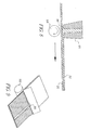
- Fig. 8 shows a cross-section view of an of a method for forming a material layer having a void using slot die coating;
- Fig. 9 shows a perspective view of a method for forming a material layer having a void using slot die coating;
- Fig. 10 is a cross-section view of an embodiment of the medium of the present invention having an overcoat layer;
- Fig. 11 is a cross-section and exploded view of the embodiment of Fig. 10;
- Fig. 12 is a cross-section view of an embodiment of the medium of the present invention having additional antenna, material and overcoat layers;
- Fig. 13 is a cross-section view of an embodiment of the medium of the present invention having an adhesive layer;
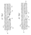
- Figs. 14 and 15 show cross sectional views of a void having walls that are shaped with features to help receive and to hold a transponder in the void.
-
- The present invention will be directed in particular to elements forming part of, or in cooperation more directly with the apparatus in accordance with the present invention. It is to be understood that elements not specifically shown or described may take various forms well known to those skilled in the art.
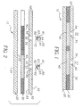
- An embodiment of the present invention will now be shown and described with reference to Figs. 1 - 3. Figs. 1 and 2 respectively show a cross-section view of one embodiment of the medium of the present invention and an exploded cross-section view of the embodiment of Fig. 1. Fig. 3 shows a top right perspective view of a base layer having an antenna layer formed thereon.
- As is shown in Figs. 1 and 2
medium 10 has abase layer 20 having atop surface 22 and abottom surface 24.Base layer 20 can be formed from a material such as a paper, plastic, metal or other convenient substrate. In certain embodiments, the material used inbase layer 20 is selected to receive image forming materials such as inks, dyes, toners, and colorants. This permits images to be formed for example onbottom surface 24 using ink jet printing, thermal printing, contact press printing and other techniques. Alternatively,base layer 20 can also be formed from a material that forms images when exposed to energy such thermal, electrical, optical, electro-magnetic or other forms. In a further alternativetop surface 22 orbottom surface 24 ofbase layer 20 can be adapted by chemical or other treatments or coatings to receive images. In the embodiment shown,base layer 20 has a thickness of approximately 100 microns however, the thickness ofbase layer 20 is not critical. - In the embodiment that is shown in Figs. 1 - 3 an
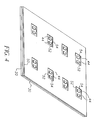
optional antenna layer 30 is formed ontop surface 22 ofbase layer 20.Antenna layer 30 typically comprises a material that is capable of being used to form an antenna. Examples of such materials include metals such as copper, aluminum and other materials having electrically conductive properties.Antenna layer 30 has patternedantennas 40 formed therein. Fig. 3 shows a top view of abase layer 20 having patternedantennas 40 applied thereon. In the embodiment shown in Figs. 1 - 3patterned antennas 40 are arranged in a first row ofantennas 32 and a second row ofantennas 34. Each one of patternedantennas 40 has an antenna section 42 and mating surfaces 44. As is shown in Fig. 3, rows ofantennas top surface 22 ofbase layer 20. However, where medium 10 has two or morepatterned antennas 40, such antennas can be arranged onantenna layer 30 in any useful pattern. - As is also shown in Fig. 3 each of patterned
antennas 40 is formed from patterns ofantenna layer 30 andspaces 36 inantenna layer 30. The arrangement ofspaces 36 that form the pattern of material comprising patternedantennas 40 can be formed by applyingantenna layer 30 totop surface 22 in a patterned fashion. This can be done for example by using printing, lamination, thermal transfer, or laser thermal transfer techniques to selectively transferantenna layer 30 totop surface 22. Alternatively,antenna layer 30 can be applied totop surface 22 to form a uniform layer, and portions ofantenna layer 30 can be selectively removed to formspaces 36. This selective removal can be done by etching or oblation processes that chemically, optically, thermally remove material fromantenna layer 30 to formspaces 36 that define patternedantennas 40. Mechanical processes can also be used to remove material fromantenna layer 30 to form patternedantennas 40. - A
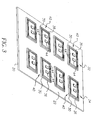
material layer 50 is applied totop surface 22 ofbase layer 20 and/or toantenna layer 30.Material layer 50 can comprise a material including paper, film, polymer or other materials. In one embodiment,material layer 50 is formed from BUTVAR polyvinyl butgral (PVB) resin sold commercially by Solutial, St. Louis, MO, USA. In the embodiments shown in Figs. 1 and 2material layer 50 is adapted to receive image forming substances such as inks, dyes, pigments, colorants, used in the formation of images. Alternatively,material layer 50 can be formed from a material that forms images when exposed to energy such as thermal, electrical optical, electromagnetic or other form.Material layer 50 can also be chemically treated to adaptmaterial layer 50 to receive images or to facilitate modification of the material layer to permit formation of images thereon. As is shown in Figs. 1 and 2, voids 52 are formed frommaterial layer 50. - Fig. 4 shows a top perspective view of
medium 10 having anantenna layer 30 coated with amaterial layer 50 havingvoids 52 formed therein. As will be seen in Fig. 4, voids 52expose antenna layer 40 so thattransponder 60 can engage antenna mating surfaces 44 onantenna layer 40 to cooperate electrically therewith. Antenna engagement surfaces 62 are provided on each of thetransponders 60 to engage mating surfaces 44. Whentransponders 60 are properly inserted invoids 52, antenna engagement surfaces 62 engagemating surfaces 44 to provide an electrical connection betweentransponders 60 and an antenna such asantenna 32. - Using this electrical connection
power supply circuits 61 intransponders 60 can receive electromagnetic signals and convert such signals into power to operates thetransponders 60. Whentransponder 60 is operated, radiofrequency communication circuit 63 uses the electrical connection between mating surfaces 44 and antenna engagement surfaces 62 to transmit radio frequency signals that contain data from amemory 65. Radiofrequency communication circuit 63 can also be adapted to use the electrical connection between engagement surfaces 62 and antenna mating surfaces 44 to receive radio frequency signals having data and to store the data from such signals inmemory 63. In embodiments that do not have an antenna layer,transponder 60 will incorporate an antenna. - In the embodiment shown in Figs. 1 - 4
voids 52 are sized to receivetransponders 60 havingwidth dimensions transponders 60. Alternatively, as will be described in greater detail below, wherematerial layer 50 is formed from a material having a degree of elasticity, thewidth dimensions voids 52 respectively can be undersized with respect to the width dimension 64 oftransponders 60. Where voids 52 are undersized, insertion oftransponders 60 intovoids 52 causes deformation ofmaterial layer 50 to allowtransponders 60 to be inserted intovoids 52.Material layer 50 resists this deformation and applies a force againsttransponders 60. This force tends to holdtransponders 60 withinvoids 52 and can be used to holdtransponders 60 so that engagement surfaces 62 remain in contact withmating surfaces 44 ofantennas 40 and do not slide along voids 52 in a manner that would cause separation of engagement surfaces 60 from mating surfaces 44. - In the embodiment shown in Figs. 1-4,
material layer 50 has athickness 58 that is at least as thick as the thickness 67 oftransponders 60. In this way, anouter surface 55 ofmaterial layer 50 and outer surfaces 69 oftransponders 60 form a common plane A - A to provide a level surface that can be processed without risk of interference with later material handling. This permits the use of useful medium fabrication processes such as rolling or extrusion aftertransponders 60 have been joined tomedium 10 and lowers the risk damage to previous and/or subsequently applied layers ofmedium 10 where medium 10 is wound onto rolls during further processing. Optionally, the portions ofvoids 52 that are not occupied bytransponders 60 can be filled with material to provide a common plane in other portions ofmedium 10 and to help secure the position oftransponders 60 invoids 52. These unoccupied portions ofvoids 52 can be filled with additional material of the type used to formmaterial layer 50. These portions can also be filled with other convenient materials such as adhesives. - Alternatively,
material layer 50 can have athickness 58 that is at least greater than the thickness 67 oftransponder 60. - A
material layer 50 havingvoid 52 can be formed on abase layer 20 and/or onantenna layer 30 using various methods. Figs. 5 - 9 show examples of these methods. Figs. 5 and 6 show an example of a gap coating method. In this method, asupply 80 of material that formsmaterial layer 50 is applied tobase layer 20 using a convenient means adapted for such material.Base layer 20 and the supply of material applied tobase layer 20 are passed between a roller 81 and limitingstructure 84 such as a knife. As the material that formsmaterial layer 50 andbase layer 20 passes between roller 81 and limitingstructure 84, excess material is scraped off. This provides auniform material layer 50 onbase layer 20. To form a void 52 inbase layer 50, astop 86 is provided in limitingstructure 84. Alternatively, stop 86 blocks material formingmaterial layer 50 from passing and creates a void 52 in thematerial layer 50. Where stop 86 is fixed, void 52 inmaterial layer 50 will have a slot shaped void extending longitudinally alongmaterial layer 50.Stop 86 can also be selectively moved into and out ofmaterial layer 50 so as to create anintermittent void 52. - Fig. 7 shows another embodiment of a method for forming a void 52 in a
material layer 50 on abase layer 20 using a technique known as curtain coating. In curtain coating, a material to be used to formmaterial layer 50 flows from asupply 88 in acontinuous curtain 90 ontobase layer 20 asbase layer 20 is passed through the flow. Astop 92 interrupts the flow fromsupply 86 in create aspace 94 incontinuous curtain 90 which results in a void 52 inmaterial layer 50. - Figs. 8 and 9 show still another embodiment of a method for forming a void in a
material layer 50. In this embodiment, a technique known as slot die coating is used. In this technique, asupply 95 has aslot 96 that ejects material ontobase layer 20 to form amaterial layer 50 thereon as thebase 20 is moved relative to slot by aroller 98. Astrip 99 interrupts the flow of the material ontobase layer 20 creating a void 52 inmaterial layer 50. It will be appreciated that other techniques can also be used to formmaterial layer 50 including but not limited to spraying and printing. - As is shown in Figs. 10 and 11, in another embodiment, an
overcoat layer 70 can be applied tomaterial layer 50.Overcoat layer 70 securestransponders 60 invoids 52. Further,overcoat layer 70 seals and fillsmaterial layer 50 so that no portion ofantenna layer 40 remains exposed afterovercoat layer 70 has been applied.Overcoat layer 70 can be applied to fill portions ofvoids 52 that are not occupied bytransponders 60. This helps to securetransponder 60 and prevent movement oftransponder 60 along voids 52.Overcoat layer 70 can be adapted to receive image-forming materials. In the embodiment that is shown in Figs. 10 and 11,overcoat layer 70 is applied to form anouter surface 72 along plane B - B that does not have protrusions or other non-uniform areas caused byspaces 36,antennas 40, voids 52 and/ortransponders 60.Overcoat layer 70 can also be adapted to cushion and protecttransponders 60,antennas 40 and medium 20 from chemical, thermal, radiation or mechanical damage during handling or manipulation ofmedium 20. - Where an
overcoat layer 70 is used, it is not essential thatmaterial layer 50 has a thickness that is at least as great as the thickness oftransponders 60. This is because a common plane e.g. B-B can be formed by anouter surface 72 ofovercoat layer 70 whereinovercoat layer 70 is applied to a thickness that, in combination withmaterial layer 50 has a thickness that is at least as thick as the thickness oftransponders 60. - Where
material layer 50 is adapted to receive image forming materials and such image forming materials can be applied to form images onmaterial layer 50 beforeovercoat layer 70 is formed. In one such embodiment,overcoat layer 70 can comprise a transparent material that blocks the flow of ultraviolet or other forms of radiation, that provides protection against mechanical, thermal, chemical or other factors that may damage the appearance of the images formed onmaterial layer 50. - As is shown in Fig. 12, an
additional antenna layer 110 can be formed onbottom surface 24 ofbase layer 20.Additional antenna layer 110 can be formed in the manner described above with respect to formingantenna layer 40. Similarly, anadditional material layer 120 can be applied toadditional antenna layer 110 withvoids 112 formed therein.Voids 112 are adapted to receivetransponders 60 and otherwise are similar tovoids 52 as described above. As is also shown in Fig. 12 anadditional overcoat layer 130 can optionally be applied toadditional material layer 90. -
Medium 10 is free ofprotrusions, thus medium 10 can be further processed as necessary using conventional web forming techniques such as winding, rolling, extruding and printing can be applied to medium 10 aftertransponder 60 has been positioned in the material layer ofmedium 10. For example, a medium 10 having atransponders 60 attached thereto can be slit and wound onto rolls with each roll having at least onetransponder 60.Medium 10 can also be slit and chopped into sheet form with each sheet having atransponder 60 associated therewith. - As is shown in Fig. 13, an adhesive layer 140 can be applied to
base layer 20 ofmedium 10 to permit medium 10 to be easily applied to a tangible thing such as a bottle. An advantage of such a medium is that a label can be provided that does not have a protrusion that might interfere with or be easily damaged by use and handling of the tangible thing to which the medium is attached. To facilitate handling of this adhesive embodiment ofmedium 10, a removable layer 150 can be applied to adhesive layer 140. - In any embodiment,
transponder 60 can be formed in whole or in part by depositing circuit forming material onmedium 20. For example,transponder 30 can be formed onbase layer 20,antenna layer 30, or inantenna layer 30 using lithographic, ink jet and other technologies that permit electronic circuits to be formed on a substrate. - In any embodiment, voids 52 can incorporate
void walls 54 that are shaped to align or otherwise positiontransponder 60 so that the antenna engagement surfaces 62 can engagemating surfaces 44 to provide an electrical connection betweentransponders 60 and an antenna such asantenna 32. The shape ofvoid walls 54 can be matched to a particular footprint of aparticular transponder 60. - Figs. 14 and 15 show cross sectional views of a void 52 having void
walls 54 that are shaped with features to help receive and to holdtransponder 60 invoid 52. As is shown, in Figs. 14 and 15void walls 54 are narrower nearouter surface 55 and wider nearinner surface 53. In this embodiment,material layer 50 is made from a material that permits some degree of elastic deformation. Accordingly, as shown in Fig. 11 when atransponder 60 is pressed into the portion ofvoid walls 54 that is nearouter surface 55,material layer 50 deforms to accepttransponder 60 into the portion ofvoid walls 54 that is nearinner surface 55. The portion ofvoid walls 54 near to the top surface ofmaterial layer 52 then elastically expands as shown in Fig. 15 to capturetransponder 30 inmaterial layer 52 in an area proximate toantenna layer 30.
Claims (10)
- A method for forming a medium comprising the steps of:providing a base layer;forming a material layer on the base layer with said material layer having a void; and,positioning a transponder having a memory in the void.
- The method of claim 1, further comprising the step of forming an antenna layer having an antenna on the base layer wherein the transponder is adapted to cooperate with the antenna when the transponder is positioned in the void.
- The method of claim 1 wherein said transponder has a thickness within a predefined range and wherein the step of forming a material layer having a void comprises forming a material layer having a thickness greater than the thickness of the transponder.
- The method of claim 1 wherein the material layer forms a void in the material layer having a width dimension that is smaller in size than a width dimension of the transponder and the step of positioning the transponder in the void comprises elastically deforming the material layer proximate to the void to receive the transponder.
- The method of claim 1, further comprising the step of providing an overcoat layer on the material layer, void and transponder.
- A method for forming a medium comprising the steps of:forming an antenna layer having an antenna on a base layer;forming a material layer on the antenna layer with said material layer having a void; and,positioning a transponder having a memory in the void wherein the transponder is adapted to cooperate with the antenna when the transponder is positioned in the void.
- A method for forming a medium, the method comprising the steps of:forming an antenna layer having an antenna on a base layer;providing a transponder having a memory and adapted to cooperate with the antenna with the transponder having a thickness;forming a material layer on the antenna layer, the material layer having a thickness that is at least equal to the thickness of the transponder and having a void sized to receive the transponder; and,positioning the transponder in the void so that the transponder can cooperate with the antenna.
- A medium comprising:a base layer;a material layer with said material layer having a void; and,a transponder having a memory in the void.
- A medium comprising:wherein the transponder is positioned in the void to cooperate with the antenna.an antenna layer forming an antenna on a base layer,a transponder with having a memory and an interface patterned to cooperate with the antenna, the transponder having a thickness; anda material layer on the antenna layer, the material layer having a void sized to receive the transponder;
- The medium of claim 9 further comprising an overcoat layer on the medium layer with the overcoat layer adapted to permit the formation of an image thereon.
Applications Claiming Priority (2)
| Application Number | Priority Date | Filing Date | Title |
|---|---|---|---|
| US10/256,769 US7233498B2 (en) | 2002-09-27 | 2002-09-27 | Medium having data storage and communication capabilities and method for forming same |
| US256769 | 2002-09-27 |
Publications (2)
| Publication Number | Publication Date |
|---|---|
| EP1406209A2 true EP1406209A2 (en) | 2004-04-07 |
| EP1406209A3 EP1406209A3 (en) | 2006-05-31 |
Family
ID=31993513
Family Applications (1)
| Application Number | Title | Priority Date | Filing Date |
|---|---|---|---|
| EP03077890A Withdrawn EP1406209A3 (en) | 2002-09-27 | 2003-09-15 | Non-contact card with transponder placed in cavity of the card |
Country Status (3)
| Country | Link |
|---|---|
| US (1) | US7233498B2 (en) |
| EP (1) | EP1406209A3 (en) |
| JP (1) | JP2004139583A (en) |
Cited By (5)
| Publication number | Priority date | Publication date | Assignee | Title |
|---|---|---|---|---|
| WO2006034355A2 (en) | 2004-09-21 | 2006-03-30 | International Business Machines Corporation | METHOD OF COLLECTOR FORMATION IN BiCMOS TECHNOLOGY |
| WO2006084984A1 (en) | 2005-02-11 | 2006-08-17 | Smart Packaging Solutions (Sps) | Method of producing a contactless microelectronic device, such as for an electronic passport |
| WO2006127773A1 (en) * | 2005-05-24 | 2006-11-30 | V.H. Blackinton And Co., Inc. | Badge verification device |
| WO2008037592A1 (en) * | 2006-09-26 | 2008-04-03 | Advanced Micromechanic And Automation Technology Ltd | Method of connecting an antenna to a transponder chip and corresponding transponder inlay |
| US8608080B2 (en) | 2006-09-26 | 2013-12-17 | Feinics Amatech Teoranta | Inlays for security documents |
Families Citing this family (16)
| Publication number | Priority date | Publication date | Assignee | Title |
|---|---|---|---|---|
| US6951596B2 (en) * | 2002-01-18 | 2005-10-04 | Avery Dennison Corporation | RFID label technique |
| US7755484B2 (en) * | 2004-02-12 | 2010-07-13 | Avery Dennison Corporation | RFID tag and method of manufacturing the same |
| US7500307B2 (en) * | 2004-09-22 | 2009-03-10 | Avery Dennison Corporation | High-speed RFID circuit placement method |
| US7623034B2 (en) * | 2005-04-25 | 2009-11-24 | Avery Dennison Corporation | High-speed RFID circuit placement method and device |
| US20060292946A1 (en) * | 2005-06-22 | 2006-12-28 | Perfect Plastic Printing Corporation | Financial Transaction Card With Embedded Fabric |
| US7224278B2 (en) | 2005-10-18 | 2007-05-29 | Avery Dennison Corporation | Label with electronic components and method of making same |
| US7740179B2 (en) * | 2005-12-15 | 2010-06-22 | Mediamark Research, Inc. | System and method for RFID-based printed media reading activity data acquisition and analysis |
| US7959086B2 (en) * | 2005-12-15 | 2011-06-14 | Gfk Mediamark Research & Intelligence, Llc | System and method for RFID-based printed media reading activity data acquisition and analysis |
| US7555826B2 (en) | 2005-12-22 | 2009-07-07 | Avery Dennison Corporation | Method of manufacturing RFID devices |
| US7701352B2 (en) * | 2006-11-22 | 2010-04-20 | Avery Dennison Corporation | RFID label with release liner window, and method of making |
| WO2009061968A1 (en) * | 2007-11-06 | 2009-05-14 | Ian Rex Binmore | Rfid transponder enclosure for harsh enviroments |
| US8094028B2 (en) * | 2007-12-28 | 2012-01-10 | Mckesson Automation, Inc. | Radio frequency alignment object, carriage and associated method of storing a product associated therewith |
| US8400277B2 (en) * | 2009-03-30 | 2013-03-19 | Mckesson Automation Inc. | Methods, apparatuses, and computer program products for monitoring a transfer of fluid between a syringe and a fluid reservoir |
| CN102714054B (en) * | 2009-11-02 | 2015-04-22 | V·V·列昂季耶夫 | Information storage and processing device |
| US9171246B2 (en) | 2012-06-29 | 2015-10-27 | Aesynt Incorporated | System, methods, apparatuses, and computer program products for detecting that an object has been accessed |
| EP3432224B1 (en) * | 2016-03-18 | 2022-06-29 | Sato Holdings Kabushiki Kaisha | Method for manufacturing an rfid inlet |
Citations (4)
| Publication number | Priority date | Publication date | Assignee | Title |
|---|---|---|---|---|
| WO1998009252A1 (en) * | 1996-08-26 | 1998-03-05 | Tomas Meinen | Process for manufacturing chip cards |
| FR2775533A1 (en) * | 1998-02-27 | 1999-09-03 | Gemplus Sca | ELECTRONIC DEVICE WITH CONTACTLESS ELECTRONIC MEMORY, AND METHOD FOR MANUFACTURING SUCH A DEVICE |
| DE20014076U1 (en) * | 2000-08-11 | 2000-10-19 | Reiner Kartengeraete Gmbh & Co | Chip card with adapter |
| US20010014377A1 (en) * | 1999-01-13 | 2001-08-16 | Babb Susan M. | Label having a protective cavity and method of manufacture |
Family Cites Families (104)
| Publication number | Priority date | Publication date | Assignee | Title |
|---|---|---|---|---|
| US3580565A (en) | 1968-12-11 | 1971-05-25 | Xerox Corp | Sheet feeding apparatus |
| US3713148A (en) | 1970-05-21 | 1973-01-23 | Communications Services Corp I | Transponder apparatus and system |
| US3835301A (en) | 1973-02-21 | 1974-09-10 | Helert P | Card coding and read-out system |
| US3926633A (en) | 1973-07-02 | 1975-12-16 | Peter Anderson Custer | Motion picture film soundtrack and method for production thereof |
| US4208210A (en) | 1974-12-19 | 1980-06-17 | Fuji Photo Film Co., Ltd. | Process for forming an optical soundtrack |
| US4129855A (en) | 1977-07-15 | 1978-12-12 | Rodrian J | Animal identification system |
| US4178183A (en) | 1978-07-27 | 1979-12-11 | Eastman Kodak Company | Thiazolyl coupler compositions and photographic elements suited to forming integral sound tracks |
| DE2840051A1 (en) | 1978-09-14 | 1980-03-27 | Agfa Gevaert Ag | PHOTOGRAPHIC IMMEDIATE IMAGE CAMERA |
| US4270853A (en) | 1979-03-21 | 1981-06-02 | West Electric Company, Ltd. | Sound-recording instant-printing film and camera therefor |
| US5019815A (en) | 1979-10-12 | 1991-05-28 | Lemelson Jerome H | Radio frequency controlled interrogator-responder system with passive code generator |
| US4247758A (en) | 1979-11-15 | 1981-01-27 | Rodrian James A | Animal identification and estrus detection system |
| US5196846A (en) | 1980-02-13 | 1993-03-23 | Brockelsby William K | Moving vehicle identification system |
| US4880325A (en) | 1980-03-17 | 1989-11-14 | Canon Kabushiki Kaisha | Ink ribbon cassette including means for identifying the type of ink ribbon contained therein and containing an ink ribbon having end indication means |
| US4663625A (en) | 1983-11-30 | 1987-05-05 | Motion Magnetics Inc. | Passive tag identification system and method |
| US4600280A (en) | 1984-07-16 | 1986-07-15 | Clark Lloyd D | Digital audio recording/playback system for motion picture film |
| DE3467822D1 (en) | 1984-09-28 | 1988-01-07 | Agfa Gevaert Nv | Photographic colour elements |
| US5008661A (en) | 1985-09-27 | 1991-04-16 | Raj Phani K | Electronic remote chemical identification system |
| US4742470A (en) | 1985-12-30 | 1988-05-03 | Gte Valeron Corporation | Tool identification system |
| NL8601021A (en) | 1986-04-22 | 1987-11-16 | Nedap Nv | PROGRAMMABLE RESPONDER. |
| US4806958A (en) | 1988-01-11 | 1989-02-21 | Eastman Kodak Company | Cassette/machine optically coupled interface |
| US5078523A (en) | 1988-03-04 | 1992-01-07 | Varitronic Systems, Inc. | Tape cassette with identifying circuit element for printing machine |
| US5559578A (en) | 1988-03-22 | 1996-09-24 | Hitachi, Ltd. | Electrostatic recording apparatus with electrified cap and managing system thereof |
| US5208450A (en) * | 1988-04-20 | 1993-05-04 | Matsushita Electric Industrial Co., Ltd. | IC card and a method for the manufacture of the same |
| DE3819783A1 (en) | 1988-06-10 | 1989-12-14 | Triumph Adler Ag | ELECTRONICALLY CONTROLLED TYPEWRITER, PRINTER OD. DGL. AND RIBBON CASSETTE OR TYPE WHEEL CASSETTE HERE |
| JP2752402B2 (en) | 1988-07-25 | 1998-05-18 | イーストマン コダック カンパニー | Print media container monitoring system for printers |
| US4855769A (en) | 1988-08-29 | 1989-08-08 | Polaroid Corporation | Photographic apparatus for motorized processing of instant film |
| JPH0236825U (en) | 1988-09-02 | 1990-03-09 | ||
| US4905029A (en) | 1988-09-28 | 1990-02-27 | Kelley Scott A | Audio still camera system |
| JPH02198881A (en) | 1989-01-27 | 1990-08-07 | Shimadzu Corp | Printer |
| US5049898A (en) | 1989-03-20 | 1991-09-17 | Hewlett-Packard Company | Printhead having memory element |
| US5128700A (en) | 1989-05-12 | 1992-07-07 | Minolta Camera Kabushiki Kaisha | Camera capable of recording sounds relevant to the photographing |
| DE4022696A1 (en) | 1989-07-18 | 1991-01-31 | Canon Kk | METHOD AND DEVICE FOR FORMING RECORDS BY MEANS OF A MULTICOLOR RIBBON |
| US4990092B1 (en) | 1989-08-14 | 1998-08-04 | Tonka Corp | Talking book |
| US5059126A (en) | 1990-05-09 | 1991-10-22 | Kimball Dan V | Sound association and learning system |
| US5347274A (en) | 1990-05-17 | 1994-09-13 | At/Comm Incorporated | Hazardous waste transport management system |
| US5266975A (en) | 1990-10-12 | 1993-11-30 | Seiko Epson Corporation | Ink jet printing apparatus having means for preventing excessive ink purging |
| US5184152A (en) | 1990-12-04 | 1993-02-02 | Sumimoto Electric Interconnect Products, Inc. | Printing apparatus and method for printing on an elongated member such as a tube |
| US5185315A (en) | 1991-02-21 | 1993-02-09 | Eastman Kodak Company | Making encoded dye-donor films for thermal printers |
| US5297881A (en) | 1991-05-16 | 1994-03-29 | Mitsubishi Steel Mfg. Co., Ltd. | Printing machine carriage having a magnetic encoder |
| US5956682A (en) | 1991-06-06 | 1999-09-21 | Lj Laboratories, Llc | Picture frame with associated audio messages and position sensitive or speech recognition device |
| US5268708A (en) | 1991-08-23 | 1993-12-07 | Eastman Kodak Company | Laser thermal printer with an automatic material supply |
| JP3155794B2 (en) | 1991-12-13 | 2001-04-16 | キヤノン株式会社 | Ink jet recording method and ink jet recording apparatus |
| JP2805666B2 (en) | 1991-12-13 | 1998-09-30 | ソニー株式会社 | ink ribbon |
| US5331338A (en) | 1992-01-30 | 1994-07-19 | Printware, Inc. | Web steering for an image recorder |
| US5196862A (en) | 1992-02-21 | 1993-03-23 | Eastman Kodak Company | Apparatus and method for donor sensing at the print line in a thermal printer |
| US5266968A (en) | 1992-03-27 | 1993-11-30 | Eastman Kodak Company | Non-volatile memory thermal printer cartridge |
| US5455617A (en) | 1992-03-27 | 1995-10-03 | Eastman Kodak Company | Thermal printer supply having non-volatile memory |
| US5342671A (en) | 1992-06-05 | 1994-08-30 | Eastman Kodak Company | Encoded dye receiver |
| US5310999A (en) | 1992-07-02 | 1994-05-10 | At&T Bell Laboratories | Secure toll collection system for moving vehicles |
| US5323704A (en) | 1992-07-30 | 1994-06-28 | Heidelberg-Harris Gmbh | Device for the identification of a flexible roller shell |
| US5290190A (en) | 1992-09-30 | 1994-03-01 | Mcclanahan Susan D | Talking book |
| US5504507A (en) | 1992-10-08 | 1996-04-02 | Xerox Corporation | Electronically readable performance data on a thermal ink jet printhead chip |
| US5521663A (en) | 1992-10-28 | 1996-05-28 | Norris, Iii; Wyamn J. | Sound system for still film photography |
| US5513920A (en) | 1992-10-29 | 1996-05-07 | Eastman Kodak Company | Dye donor web loading apparatus for a thermal printer |
| US5318370A (en) | 1992-11-17 | 1994-06-07 | Varitronic Systems, Inc. | Cartridge with data memory system and method regarding same |
| US5606347A (en) | 1992-12-16 | 1997-02-25 | Texas Instruments Incorporated | Devices systems and methods for flexible format data storage |
| US5305020A (en) | 1992-12-21 | 1994-04-19 | Tektronix, Inc. | Thermal transfer printer having media pre-coat selection apparatus and methods |
| US5398257A (en) | 1993-01-11 | 1995-03-14 | Groenteman; Frank S. | Copier and monitoring network |
| US5537135A (en) | 1993-01-22 | 1996-07-16 | Gerber Scientific Products, Inc. | Method and apparatus for making a graphic product |
| JP3170528B2 (en) | 1993-01-28 | 2001-05-28 | 富士写真フイルム株式会社 | Thermal recording apparatus and method having shading correction function |
| JP3292535B2 (en) | 1993-03-01 | 2002-06-17 | 理想科学工業株式会社 | Stencil printer and plate cylinder |
| DE69412691T2 (en) | 1993-04-30 | 1999-01-14 | Hewlett Packard Co | Alignment system for multiple inkjet cartridges |
| US5491468A (en) | 1993-06-24 | 1996-02-13 | Westinghouse Electric Corporation | Identification system and method with passive tag |
| US5516590A (en) | 1993-07-15 | 1996-05-14 | Ncr Corporation | Fluorescent security thermal transfer printing ribbons |
| US5412192A (en) * | 1993-07-20 | 1995-05-02 | American Express Company | Radio frequency activated charge card |
| US5430441A (en) | 1993-10-12 | 1995-07-04 | Motorola, Inc. | Transponding tag and method |
| JP3244371B2 (en) | 1993-12-22 | 2002-01-07 | オリンパス光学工業株式会社 | Audio information processing system and audio information processing method |
| JPH07186476A (en) | 1993-12-28 | 1995-07-25 | Sony Corp | Ribbon cartridge |
| US5565906A (en) | 1994-01-13 | 1996-10-15 | Schoonscan, Inc. | Clocking means for bandwise imaging device |
| US5598201A (en) | 1994-01-31 | 1997-01-28 | Hewlett-Packard Company | Dual-resolution encoding system for high cyclic accuracy of print-medium advance in an inkjet printer |
| US5528377A (en) | 1994-03-29 | 1996-06-18 | E. I. Du Pont De Nemours And Company | Extended density color printing |
| US5574519A (en) | 1994-05-03 | 1996-11-12 | Eastman Kodak Company | Talking photoalbum |
| TW280893B (en) | 1994-05-06 | 1996-07-11 | Kansai Paint Co Ltd | |
| US5530702A (en) | 1994-05-31 | 1996-06-25 | Ludwig Kipp | System for storage and communication of information |
| US5600352A (en) | 1994-06-27 | 1997-02-04 | Tektronix, Inc. | Apparatus and method for controlling coalescence of ink drops on a print medium |
| US5610635A (en) | 1994-08-09 | 1997-03-11 | Encad, Inc. | Printer ink cartridge with memory storage capacity |
| US5491327A (en) | 1994-08-10 | 1996-02-13 | American Magnetics Corporation | Universal magnetic medium encoder with tilt-compensating apparatus |
| US5528222A (en) | 1994-09-09 | 1996-06-18 | International Business Machines Corporation | Radio frequency circuit and memory in thin flexible package |
| US5493385A (en) | 1994-12-09 | 1996-02-20 | Eastman Kodak Company | Electrophotographic color printer apparatus and method with improved registration of colors |
| US5812156A (en) | 1997-01-21 | 1998-09-22 | Hewlett-Packard Company | Apparatus controlled by data from consumable parts with incorporated memory devices |
| US5584070A (en) | 1994-12-29 | 1996-12-10 | Motorola, Inc. | Wireless pager with separable receiver unit and transmitter unit |
| EP0727696B1 (en) * | 1995-02-17 | 2003-05-14 | Agfa-Gevaert | Identification system and method for use in the field of digital radiography |
| US5774639A (en) | 1995-02-17 | 1998-06-30 | Eastman Kodak Company | Printer media including compressed sensitometry curve information |
| US5721992A (en) | 1995-03-28 | 1998-02-24 | Chovanes; Joseph E. | Method and apparatus for taking still pictures |
| US5713288A (en) | 1995-08-03 | 1998-02-03 | Frazzitta; Joseph R. | Method and apparatus for use in offset printing |
| US5757394A (en) | 1995-09-27 | 1998-05-26 | Lexmark International, Inc. | Ink jet print head identification circuit with programmed transistor array |
| US6036099A (en) * | 1995-10-17 | 2000-03-14 | Leighton; Keith | Hot lamination process for the manufacture of a combination contact/contactless smart card and product resulting therefrom |
| US5647679A (en) | 1996-04-01 | 1997-07-15 | Itw Limited | Printer for printing on a continuous print medium |
| US6282819B1 (en) | 1996-06-10 | 2001-09-04 | Jing Lu Gu | Design and manufacture of communicating card |
| US5768633A (en) | 1996-09-03 | 1998-06-16 | Eastman Kodak Company | Tradeshow photographic and data transmission system |
| US5913088A (en) | 1996-09-06 | 1999-06-15 | Eastman Kodak Company | Photographic system capable of creating and utilizing applets on photographic film |
| US5755519A (en) | 1996-12-04 | 1998-05-26 | Fargo Electronics, Inc. | Printer ribbon identification sensor |
| US5842118A (en) | 1996-12-18 | 1998-11-24 | Micron Communications, Inc. | Communication system including diversity antenna queuing |
| US5774752A (en) | 1996-12-26 | 1998-06-30 | Eastman Kodak Company | Processing of sound media with still image films in photofinishing labs |
| US5914671A (en) | 1997-02-27 | 1999-06-22 | Micron Communications, Inc. | System and method for locating individuals and equipment, airline reservation system, communication system |
| US6227643B1 (en) | 1997-05-20 | 2001-05-08 | Encad, Inc. | Intelligent printer components and printing system |
| FR2769440B1 (en) * | 1997-10-03 | 1999-12-03 | Gemplus Card Int | METHOD FOR MANUFACTURING AN ELECTRONIC CHIP AND / OR ANTENNA DEVICE AND DEVICE OBTAINED BY THE METHOD |
| US6099178A (en) | 1998-08-12 | 2000-08-08 | Eastman Kodak Company | Printer with media supply spool adapted to sense type of media, and method of assembling same |
| US6075950A (en) | 1998-09-22 | 2000-06-13 | Eastman Kodak Company | Associating a sound record with a film image |
| US6404643B1 (en) * | 1998-10-15 | 2002-06-11 | Amerasia International Technology, Inc. | Article having an embedded electronic device, and method of making same |
| US6100804A (en) * | 1998-10-29 | 2000-08-08 | Intecmec Ip Corp. | Radio frequency identification system |
| US6173119B1 (en) | 1999-08-11 | 2001-01-09 | Eastman Kodak Company | Camera having radio-frequency identification transponder |
| US6106166A (en) | 1999-04-16 | 2000-08-22 | Eastman Kodak Company | Photoprocessing apparatus for sensing type of photoprocessing consumable and method of assembling the apparatus |
| US7664296B2 (en) * | 2001-01-31 | 2010-02-16 | Fujifilm Corporation | Image recording method and system, image transmitting method, and image recording apparatus |
-
2002
- 2002-09-27 US US10/256,769 patent/US7233498B2/en not_active Expired - Fee Related
-
2003
- 2003-09-15 EP EP03077890A patent/EP1406209A3/en not_active Withdrawn
- 2003-09-24 JP JP2003332062A patent/JP2004139583A/en active Pending
Patent Citations (4)
| Publication number | Priority date | Publication date | Assignee | Title |
|---|---|---|---|---|
| WO1998009252A1 (en) * | 1996-08-26 | 1998-03-05 | Tomas Meinen | Process for manufacturing chip cards |
| FR2775533A1 (en) * | 1998-02-27 | 1999-09-03 | Gemplus Sca | ELECTRONIC DEVICE WITH CONTACTLESS ELECTRONIC MEMORY, AND METHOD FOR MANUFACTURING SUCH A DEVICE |
| US20010014377A1 (en) * | 1999-01-13 | 2001-08-16 | Babb Susan M. | Label having a protective cavity and method of manufacture |
| DE20014076U1 (en) * | 2000-08-11 | 2000-10-19 | Reiner Kartengeraete Gmbh & Co | Chip card with adapter |
Cited By (10)
| Publication number | Priority date | Publication date | Assignee | Title |
|---|---|---|---|---|
| WO2006034355A2 (en) | 2004-09-21 | 2006-03-30 | International Business Machines Corporation | METHOD OF COLLECTOR FORMATION IN BiCMOS TECHNOLOGY |
| WO2006084984A1 (en) | 2005-02-11 | 2006-08-17 | Smart Packaging Solutions (Sps) | Method of producing a contactless microelectronic device, such as for an electronic passport |
| FR2882174A1 (en) * | 2005-02-11 | 2006-08-18 | Smart Packaging Solutions Sps | METHOD FOR MANUFACTURING A MICROELECTRONIC DEVICE WITH NON-CONTACT FUNCTIONING, IN PARTICULAR FOR ELECTRONIC PASSPORT |
| US7992790B2 (en) | 2005-02-11 | 2011-08-09 | Smart Packaging Solutions (Sps) | Method of producing a contactless microelectronic device, such as for an electronic passport |
| RU2464635C2 (en) * | 2005-02-11 | 2012-10-20 | Смарт Пэкэджинг Солюшнс (Спс) | Method of producing contactless microelectronic device, particularly for electronic passport |
| CN101203869B (en) * | 2005-02-11 | 2016-03-30 | 智能包装技术公司 | For the manufacture method of the contactless microelectronic device of E-Passport etc. |
| WO2006127773A1 (en) * | 2005-05-24 | 2006-11-30 | V.H. Blackinton And Co., Inc. | Badge verification device |
| US7522056B2 (en) | 2005-05-24 | 2009-04-21 | V.H. Blackinton & Co., Inc. | Badge verification device |
| WO2008037592A1 (en) * | 2006-09-26 | 2008-04-03 | Advanced Micromechanic And Automation Technology Ltd | Method of connecting an antenna to a transponder chip and corresponding transponder inlay |
| US8608080B2 (en) | 2006-09-26 | 2013-12-17 | Feinics Amatech Teoranta | Inlays for security documents |
Also Published As
| Publication number | Publication date |
|---|---|
| US7233498B2 (en) | 2007-06-19 |
| EP1406209A3 (en) | 2006-05-31 |
| US20040061994A1 (en) | 2004-04-01 |
| JP2004139583A (en) | 2004-05-13 |
Similar Documents
| Publication | Publication Date | Title |
|---|---|---|
| US7233498B2 (en) | Medium having data storage and communication capabilities and method for forming same | |
| US6851617B2 (en) | Laser imageable RFID label/tag | |
| US6557766B1 (en) | Hot lamination method for a hybrid radio frequency optical memory card converting sheets into a web process | |
| US7159298B2 (en) | Method for the formation of RF antennas by demetallizing | |
| US7997496B2 (en) | Laminated printable multi-layer card with entrapped security element | |
| EP1506635B1 (en) | Method of making secure personal data card | |
| US20040062016A1 (en) | Medium having data storage and communication capabilites and method for forming same | |
| CN110267806B (en) | Composite laminate assembly for forming a plurality of individual cards and method of making same | |
| JP4590908B2 (en) | Non-contact IC medium and method of manufacturing non-contact IC medium | |
| JPWO2006077689A1 (en) | IC card manufacturing method | |
| JP2005222277A (en) | Information recording medium | |
| JP4048788B2 (en) | card | |
| JP4882187B2 (en) | Contactless IC card and contactless IC card sending medium | |
| JP4163579B2 (en) | Non-contact IC label | |
| JP4529486B2 (en) | Non-contact IC media | |
| JPH08123926A (en) | Information storage carrier and production thereof | |
| US20210039423A1 (en) | Ribbon impresser/indenter for plastic cards | |
| JP4028223B2 (en) | card case | |
| EP2343673A2 (en) | Document incorporating an RFID device and manufacturing method thereof | |
| JP2007047937A (en) | Ic card and manufacturing method of ic card | |
| JP2003067716A (en) | Non-contact ic card, non-contact ic card transmission medium, and their manufacturing method | |
| JP2005284813A (en) | Manufacturing method for rf-id medium | |
| JP4259973B2 (en) | Method for manufacturing RF-ID media | |
| JP2007011441A (en) | Ic card | |
| JP2011150409A (en) | Security document |
Legal Events
| Date | Code | Title | Description |
|---|---|---|---|
| PUAI | Public reference made under article 153(3) epc to a published international application that has entered the european phase |
Free format text: ORIGINAL CODE: 0009012 |
|
| AK | Designated contracting states |
Kind code of ref document: A2 Designated state(s): AT BE BG CH CY CZ DE DK EE ES FI FR GB GR HU IE IT LI LU MC NL PT RO SE SI SK TR |
|
| AX | Request for extension of the european patent |
Extension state: AL LT LV MK |
|
| PUAL | Search report despatched |
Free format text: ORIGINAL CODE: 0009013 |
|
| AK | Designated contracting states |
Kind code of ref document: A3 Designated state(s): AT BE BG CH CY CZ DE DK EE ES FI FR GB GR HU IE IT LI LU MC NL PT RO SE SI SK TR |
|
| AX | Request for extension of the european patent |
Extension state: AL LT LV MK |
|
| AKX | Designation fees paid | ||
| REG | Reference to a national code |
Ref country code: DE Ref legal event code: 8566 |
|
| STAA | Information on the status of an ep patent application or granted ep patent |
Free format text: STATUS: THE APPLICATION IS DEEMED TO BE WITHDRAWN |
|
| 18D | Application deemed to be withdrawn |
Effective date: 20061202 |