EP1408643B1 - Phase detector having improved timing margins - Google Patents
Phase detector having improved timing margins Download PDFInfo
- Publication number
- EP1408643B1 EP1408643B1 EP03011844A EP03011844A EP1408643B1 EP 1408643 B1 EP1408643 B1 EP 1408643B1 EP 03011844 A EP03011844 A EP 03011844A EP 03011844 A EP03011844 A EP 03011844A EP 1408643 B1 EP1408643 B1 EP 1408643B1
- Authority
- EP
- European Patent Office
- Prior art keywords
- input
- clock
- gate
- data
- data signals
- Prior art date
- Legal status (The legal status is an assumption and is not a legal conclusion. Google has not performed a legal analysis and makes no representation as to the accuracy of the status listed.)
- Expired - Fee Related
Links
Images


Classifications
-
- H—ELECTRICITY
- H04—ELECTRIC COMMUNICATION TECHNIQUE
- H04L—TRANSMISSION OF DIGITAL INFORMATION, e.g. TELEGRAPHIC COMMUNICATION
- H04L7/00—Arrangements for synchronising receiver with transmitter
- H04L7/02—Speed or phase control by the received code signals, the signals containing no special synchronisation information
- H04L7/033—Speed or phase control by the received code signals, the signals containing no special synchronisation information using the transitions of the received signal to control the phase of the synchronising-signal-generating means, e.g. using a phase-locked loop
-
- H—ELECTRICITY
- H03—ELECTRONIC CIRCUITRY
- H03L—AUTOMATIC CONTROL, STARTING, SYNCHRONISATION, OR STABILISATION OF GENERATORS OF ELECTRONIC OSCILLATIONS OR PULSES
- H03L7/00—Automatic control of frequency or phase; Synchronisation
- H03L7/06—Automatic control of frequency or phase; Synchronisation using a reference signal applied to a frequency- or phase-locked loop
- H03L7/08—Details of the phase-locked loop
- H03L7/085—Details of the phase-locked loop concerning mainly the frequency- or phase-detection arrangement including the filtering or amplification of its output signal
- H03L7/091—Details of the phase-locked loop concerning mainly the frequency- or phase-detection arrangement including the filtering or amplification of its output signal the phase or frequency detector using a sampling device
Definitions
- This invention relates to phase detectors and more particularly to a system and method for clock recovery from non-return-to-zero (NRZ) data and even more particularly to such a system and method for an improved timing margin half-rate continuous phase detector.
- NRZ non-return-to-zero
- phase detectors Two classes of phase detectors are in common use, commonly referred to as “bang-bang” and “continuous.”
- the bang-bang circuits are derived from Alexander's original design, as discussed in Alexander, JDH, "Clock Recovery from Random Binary Signals," Electronic Letters, v. 11, n. 32, pp 541-542, Oct. 30, 1975 .
- the bang-bang class has a binary quantized output that only indicates whether the clock is "early” or “late,” but not by how much. This results in the control loop operating in a discontinuous or "bang-bang” mode, which adds spurious jitter to the recovered clock and thus argues against the use of bang-bang phase detectors in jitter measurement systems. Also, in communications systems, this spurious jitter reduces the performance of the system.
- the continuous phase detectors are patterned after, or emulate, Hogge's original design as discussed in Hogge, CP, "A Self Correcting Clock Recovery Circuit," Journal of Lightwave Technology, v. LT-3, n. 6, pp 1312-1314, Dec. 1985 . These detectors have an output that can be used to generate a voltage proportional to phase error, thus resulting in a "proportional" mode for the control loop. This is much more desirable in operational systems and essential in jitter measurement systems. However, many systems operating at state-of-the-art clock rates still use bang-bang phase detectors because they will operate considerably faster than continuous phase detectors, for a given logic hardware technology. This is because the timing is more critical in the continuous phase detectors of known design.
- phase detectors described above are clocked at "full rate,” meaning that the clock frequency is equal to the baud rate of the data. For example, if the data is at a 10 Gbit/s rate (10 10 baud), and the clock is 10 GHz, the circuit is described as being clocked at “full rate.” In this context, “half rate” clocking would refer, for example, to 10 Gbit/s data with a 5 GHz clock.
- the present invention provides a circuitry for providing an output representative of input data signals and clock signals according to claim 1.
- Preferred embodiments of the invention are defined in dependent claims.
- the present invention is directed to a phase detector constructed from a plurality of multi-input gates which combine combinations of unretimed input data with retimed data and with clock signals to achieve output pulses proportional to the phase difference between the unretimed data and the clock.
- the phase detector comprises an input for receiving data signals; an input for receiving clock signals; an output for providing phase control signals; data retiming circuiting for accepting unretimed data signals from said data input and for providing even and odd retimed signals therefrom; a plurality of multi-input gates having inputs connected to different combinations of said unretimed data signals, said retimed data signals, and said clock signals, such that no said gate can be active in two consecutive UIs, when a UI is defined as the length of time allocated to a single bit; and a combiner for mixing the outputs of at least two of said gates.
- FIGURE 1 shows one embodiment of an illustrative example of the invention
- FIGURE 2 shows the embodiment of FIGURE 1 with the addition of a reference output
- FIGURE 3A, 3B and 3C show timing diagrams for the circuit of FIGURE 1;
- FIGURE 4 shows timing diagrams of the circuit of FIGURE 1 for the situation where the rise and fall time of the output pulses is significant;
- FIGURE 6 shows another embodiment of the invention
- FIGURES 7 and 8 show timing diagrams of the circuit of FIGURE 6
- FIGURE 9A, 9B and 9C show prior art timing diagrams for full-rate clock
- FIGURES 10A, 10B, and 10C show prior art timing diagrams for half-rate clock
- FIGURES 11A and 11B show prior art flip-flop timing
- FIGURES 12A and 12B show prior art later timing
- FIGURE 13 shows prior art master/slave flip-flip constructed from two latches
- FIGURES 14A, 14B, and 14C show a prior art multiplexer and its timing
- FIGURES 15A, 15B, and 15C show a prior art demultiplexer and its timing
- FIGURES 16A, 16B, and 16C show a prior art half-rate retimer and its timing
- FIGURES 17A, 17B, 17C and 17D show a prior art phase detector and its timing
- FIGURES 18A and 18B show a prior art reference output and its timing
- FIGURES 19A and 19B show a prior art half-rate phase detector and its timing
- FIGURES 20A, 20B, 20C and 20D show a prior art half-rate phase detector and its timing.
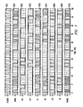
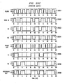
- Figures 9A, 9B and 9C are timing diagrams for full-rate operation showing clock waveforms 901 A, 901B, and 901C idealized as a square wave, and data 902A, 902B, and 902C idealized as instantaneously changing state at each bit boundary.
- the length of time allotted for a single bit is called a unit interval (UI).
- the optimum time to sample the data is at the center of the UI representing the bit, as shown by 903A and 903A', in FIGURE 9A.
- FIGURE 9B shows sample time 903B and 903B' as being early
- FIGURE 9C shows sample time 903C and 903C' as being late.
- the data is normally captured by an edge-triggered D-type flip-flop, which can be thought of as a sampler that samples the data at the time of a positive going transition of the clock (903A, 903B, 903C).
- edge-triggered D-type flip-flop which can be thought of as a sampler that samples the data at the time of a positive going transition of the clock (903A, 903B, 903C).
- the clock and data transitions should be spaced 1 ⁇ 2 UI apart.
- FIGURES 10A, 10B and 10C are similar to FIGURES 9A, 9B and 9C, except they show the half-rate clock operation.
- data 1002A, 1002B, and 1002C are sampled at every clock transition 1003A, 1003A', 1003B, 1003B', 1003C, and 1003C', whether positive or negative.
- clock transitions of clock signal 1001 A, 1001B and 1001C are 1 UI apart.
- Jitter refers to variation in the clock phase (the relationship of the clock signal to the data signal) from bit to bit. If clock phase is thought of statistically as a random variable, then jitter is a measure (similar to variance) of the "randomness" of the variable. While the clock phase may be correct on the average, it can vary considerably for any particular bit. If a jittery data signal is sampled at uniform intervals, instead of the sampling taking place in the middle of a bit, it will be early some of the time and late some of the time. This timing error makes the system more vulnerable to bit errors due to noise and other impairments.
- jitter Another way of thinking of jitter is to consider clock phase to be a signal. Then jitter represents noise added to this phase signal. Jitter is closely related to "phase noise,” which is a measure of spurious phase modulation of a sine wave.
- a straightforward jitter mechanism is that the clock signal itself has jitter on it, and the device generating the data will inherit this jitter. This jitter mechanism is independent of the characteristics of the data being transferred.
- a second jitter mechanism is called "data pattern jitter.” In this case, the timing of data will be corrupted while passing through a data transfer device due to group delay impairments in the device, which occur even in the presence of a perfect clock. Its name derives from the fact that the characteristics of the jitter depend on the characteristics of the data being transferred.
- phase detectors are built from hierarchically organized combinations of circuit blocks, rather than as being an unrelated collections of gates and other elements.
- FIGURE 11A shows D flip-flop 1100 (henceforth referred to simply as a "flip-flop"), and FIGURE 11B shows its timing diagram.
- the basic function of flip-flop 1100 is to take in data 1101 at the D input and send the data back out of the Q output to output lead 1102, under the control of clock 1103.
- clock transition 1104 FIGURE 11B
- the D input is low
- the output will go low 1105 (or stay low if it was already low).
- the D input is high at a positive clock transition 1106, 1107
- the output will go high 1108 (or stay high if it was already high).
- the flip-flop does nothing.
- a flip-flop can be thought of as a data retimer.
- the unretimed data at the D input to the flip-flop has a moderate amount of jitter on it.
- the flip-flop will, in general, sample the data at non-optimum times, but will still arrive at the correct value for each bit. It will then reproduce these bits at the output, however the timing of them will be controlled by the clock, not the time of arrival at the input.
- a perfect flip-flop, with a perfect clock will retime data so as to remove all jitter.
- a flip-flop may either increase or decrease jitter.
- unretimed data the input data to a flip-flop
- retimed data the output data from a flip-flop
- FIGURE 12A shows D latch 1200 (henceforth referred to simply as a "latch") and FIGURE 12B show its timing diagram.
- Latches are important in general because they are building blocks for flip-flops and specifically because they are used explicitly in the aforementioned Savoj et al paper.
- the basic function of the flip-flop is to take in data 1201 at the D input and send the data back out of Q output 1202.
- the latch is controlled by a latch input 1203 instead of a clock input, and its behavior is slightly different than a flip-flop. It has two modes, depending on the state of the latch input. When the latch input is low 1204, the latch is in track mode.
- Track mode is a straight-through transfer mode, in which the output responds immediately to the input.
- the latch input goes high, the latch goes to latch mode.
- latch mode the output is latched in whatever state it had upon leaving track mode.
- the latch input transitions from high to low 1206, returning the latch to track mode.
- the output state immediately changes (if necessary) to be the same as the current input state, and follows any input changes after that.
- FIGURE 13 shows how flip-flop 1300 can be constructed using two latches 1200 and 1200' When made this way, it is called a master-slave flip-flop.
- Master latch 1200 operates from clock input 1302 and slave latch 1200' operates from the complement (via inverter 1301) of the clock input. Therefore, when the clock is low, the master tracks and the slave latches. When the clock goes high, the master latches and the slave tracks. Operation is as follows: the master latch latches the unretimed data 1303 on positive clock transitions, and feeds it to the slave latch.
- the slave latch currently in track mode, passes the data through to the output. On the next negative clock edge, the slave latches the data at the output to hold it. Meanwhile, the master latch begins to track the current state of the unretimed data.
- each operation must take place in less than 1 ⁇ 2 of a clock period. If a full rate clock is used, 1 ⁇ 2 of a clock period is 1 ⁇ 2 UI. This requires the constituent latches to be able to operate at twice the data rate. If a half rate clock is used, 1 ⁇ 2 of a clock period is 1 UI. This merely requires the constituent latches to be able to operate at the data rate.
- a 1:2 demultiplexer (for the purposes of discussion herein) is a device that splits an unretimed data signal into two retimed output data signals, with the output data rate being half of the input data rate. Its basic function is to slow down data so that it can be processed at a lower rate by slower hardware.
- FIGURE 14A and 14B show how demultiplexer 1400 (FIGURE 14C) can be constructed from two flip-flops 1300 and 1300'.
- a half-rate clock 1401 is used for one flip-flop, (denoted “even"), and the complement of that half-rate clock 1401' is used for the other flip-flop, (denoted “odd”).
- Flip-flop 1300 samples unretimed data 1402 on positive going clock edges, while flip-flop 1300' samples unretimed data on negative going clock edges.
- the sampled data is at half the rate of the unretimed data.
- Retimed data is alternately transferred to "even" output 1403, then to "odd” output 1404. Thus, even numbered bits go to the even output and odd numbered bits go to the odd output.
- a 2:1 multiplexer does the reverse operation by combining two half-rate data inputs into one full rate data input.
- FIGURES 15A and 15B show that 2:1 multiplexer 1500 (FIGURE 15C) is simply a data selector switch driven by a half-rate clock. When half-rate clock 1501 is high, one input is switched through to output 1701; when the clock is low, the other input is switched through to output 1701. The complementary clock signals are generated by inverter 1703. The data switch is easily constructed using combinatorial logic.
- a multiplexer inherently retimes the data.
- FIGURES 16A and 16B show that it is also possible to combine 1:2 demultiplexer 1400 with 2:1 multiplexer 1500 to form half-rate retimer 1600, the symbol for which is shown in FIGURE 16C.
- the multiplexing function undoes the de-multiplexing function; the result is that the circuit merely retimes the data.
- data in 1601 is retimed as data out 1603, as shown in FIGURE 16B.
- It performs essentially the same function in terms of retiming data as a flip-flop; the main difference is that it operates from half-rate clock 1602, and the internal operation of the retimer is at half the rate of the flip-flop. Thus, it potentially can operate at a higher speed.
- a half-rate retimer is sometimes referred to as a double-edge triggered flip-flop because it responds to both positive and negative clock edges.
- Circuit 1700 shown in FIGURE 17A retimes the unretimed data with a conventional flip-flop 1200 (FIGURE 12), clocked at full rate by clock 1702.
- An exclusive-OR gate 1705 compares retimed data 1703 to unretimed data 1701.
- Output 1704 of the gate consists of pulses with duration proportional to the phase of clock 1702.
- a pulse is produced only when there is a data transition from which to gather phase information.
- the pulses are 1 ⁇ 2 UI long, as shown by the pulses designated as 1706 in FIGURE 17B.
- the pulses narrow as shown by the pulses designated as 1707 on FIGURE 17C.
- the pulses designated 1708 in FIGURE 17D The pulses can be smoothed by a low pass filter to produce a voltage proportional to phase.
- Circuit 1700 has at least four serious limitations. (1).
- the flip-flop must operate at the full clock rate.
- the effective data rate of the phase output is twice the data rate of the unretimed data. This immediately limits the maximum clock rate to half the maximum switching rate capability of the underlying logic technology.
- the circuit does not compare the unretimed data timing directly against the clock. Instead the unretimed data timing is compared against the retimed data at the output of the flip-flop. The retimed data serves as a proxy for the clock timing.
- any jitter, propagation delay drift, or other inaccuracy inherent in the flip-flop degrades output accuracy.
- a significant, but often overlooked, source of error in flip-flops operating near their maximum rate is a dependence of propagation delay on the amount of set up time at the data input.
- circuit 1800 shown in FIGURE 18A adds an additional "reference" output 1805 that generates a shifting reference voltage that has the same dependency on data transition density, but is independent of phase.
- the reference output consists of pulses with fixed duration of 1 ⁇ 2 UI generated after each data transition.
- the reference output is subtracted from the phase output, resulting in a corrected output that is always zero (on the average) when the phase error is zero.
- the reference output like the phase output, must operate at twice the rate of the unretimed data, which again limits the maximum clock rate.
- FIGURE 18B shows the timing for circuit 1800 with respect to data in 1801, clocks in 1802, Q1 1803, Q2 1804, and reference out 1805.
- the output from flip-flops 1810, 1811 are supplied to exclusive OR (XOR) gate 1806.
- Phase detector 1900 shown in FIGURE 19A replaces the full-rate flip-flop with half-rate retimer 1600.
- the operation of exclusive-OR gate 1906 to generate pulses 1903 having duration proportional to phase is identical to that described with respect to circuit 1700.
- the major advantage circuit 1900 over circuit 1700 is that the retiming function is now done at half-rate, which addresses limitation (1) discussed above. Limitations (2) through (4) remain.
- FIGURE 19B shows the timing for circuit 1900 with respect to data in 1901, clock 1902, data out 1903 and phase out 1904.
- FIGURE 20A shows the phase detector described in the above-identified Savoj et al reference
- FIGURE 20B shows its timing diagram for optimum clock phase with respect to, clock 2001, data in 2002, Y1 2003, X2 2005, phase out 2007, Y1 2004, Y2 2006 and reference out 2008.
- the circuit operates from half-rate clock 2001. It uses four latches 2010-2012 organized into a 1:2 demultiplexer using the architecture previously described.
- the multiplexer outputs supply the recovered data, which also drives exclusive-OR gate 2015 to produce reference output pulses 2008. Note that these reference pulses are of 1 UI duration, in contrast to circuit 1800 in which they are of 1 ⁇ 2 UI duration.
- the two master latch outputs are brought out separately to another exclusive-OR gate 2014 that produces the phase output pulses 2007.
- FIGURE 20B shows that the output of the latches 2007 contains 1 ⁇ 2 UI duration pulses. These pulses must then propagate through exclusive-OR gate 2015.
- the pulse duration decreases to less than 1 ⁇ 2 UI.
- the output pulse duration becomes impractically small, as shown by graph 2007, FIGURE 20C and the output pulses are no longer accurately produced, resulting in phase detector measurement error.
- the pulse duration increases to more than 1 ⁇ 2 UI.
- the gap between them decreases to less than 1 ⁇ 2 UI, as shown by graph 2007 FIGURE 20D.
- the pulse duration becomes impractically small, and the output pulses are no longer accurately produced, again resulting in phase detector measurement error.
- narrow pulses appear at nodes X1 and X2 (graphs 2003, 2004, FIGURE 20D). These narrow pulses must propagate through the exclusive-OR gate. Extremely narrow pulses tend to change their duration after propagating through a gate. This change of duration is another source of inaccuracy.
- the reference output works in a somewhat different manner than the phase detector.
- the even demultiplexed data is compared to the odd demultiplexed data by a second exclusive-OR gate.
- the gate produces a 1 UI pulse after each data transition.
- these pulses are averaged, they produce exactly twice the voltage as the reference pulses of circuit 1800.
- this voltage is attenuated by a factor of 2 before being subtracted from the phase output. Because of the doubled pulse duration, the reference output actually attains the full benefit of the half-rate clocking.
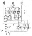
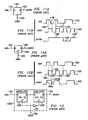
- FIGURE 1 shows the schematic of a first embodiment 10.
- the data recovery is done, for example, by a conventional half rate 1:2 demultiplexer, consisting of two flip-flops 111, 112 (FF1 and FF2) clocked on opposite clock edges of clock signal 100.
- the master latch outputs are not broken out separately.
- retimed data 102 is combined with delayed versions of unretimed data 113 and delayed versions of clock signal 105 by, in this embodiment, a bank of four 3-input AND gates 115, 116, 117, 118 (U1 through U4).
- the outputs of the gates are summed together by linear passive combiner 121 to form phase output 110.
- a "bubble" at the input of the AND gates denotes an inversion. Also note that all gates operate at half rate or less.
- FIGURE 2 shows the addition of XOR gate 1806 to generate a reference output as described with respect to FIGURE 18A.
- This gate (or other circuitry) may be conveniently added onto the circuit of FIGURE 1 to make a complete working system, since both designs are based on a 1:2 demultiplexer.
- Data bits that are valid during a positive clock edge are defined as “even” bits.
- Data bits that are valid during a negative clock edge are defined as “odd” bits.
- Data transitions that begin with an even bit and end with an odd bit are defined as “even transitions.”
- Data transitions that begin with an odd bit and end with an even bit are defined as “odd transitions.”
- Data transitions that begin with a 0 bit and end with a 1 bit are defined as “positive transitions.”
- Data transitions that begin with a 1 bit and end with a 0 bit are defined as "negative transitions.”
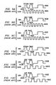
- FIGURE 3A shows the timing diagram (optimum clock phase) for circuit 10 (without optional low pass filters 120).
- figures 3B and 3C show the timing for late and early phase, respectively.
- the delay ⁇ through the flip-flop will be assumed to be zero. The effect of non-zero ⁇ delay will be discussed hereinafter.
- FF1 111 processes even data
- FF2 112 processes odd data.
- the retimed data (or complement thereof) is combined with the unretimed data (or complement thereof) and the clock (or complement thereof) in various combinations by AND gates 115-118 (U1-U4).
- gate U1 generates a pulse at each even, negative transition.
- Gate U2 generates a pulse at each even, positive transition.
- Gate U3 generates a pulse at each odd, negative transition and gate U4 generates a pulse at each odd, positive transition.
- the duration of the pulses from gates U1-U4 is proportional to phase.
- the pulses are optionally low pass filtered by filter 120, then summed by linear combiner 121, resulting in a phase output that consists of a pulse proportional to phase at every data transition.
- Phase signal 110 in FIGURES 3A, 3B, and 3C is for the case of no low pass filter 120. The effect of a low pass filter will be discussed hereinafter.
- the output combining is explained in more detail below. This output is functionally the same as the outputs discussed above with respect to the prior art, and thus circuit 10 is a direct replacement therefore.
- gate U3 puts out pulses that begin on a negative data transition and end on a positive clock transition.
- the U2 and U3 pulses alternate in time and are summed by combiner 121.
- the pulse duration depends on the time interval between data and clock, which is proportional to phase.
- No gate can be active during two consecutive UI's, because of the following mathematical properties: (1) positive and negative transitions always alternate (although there can be UI's in-between without transitions); (2) transitions occurring in consecutive UI's cannot both be even or both be odd. Therefore, any individual gate operates at half rate (or less), and always has at least 1 UI of dead time between pulses.
- the outputs of gates U1-U4 could simply be combined by a four-input OR gate, (instead of the linear combiner actually used), to produce the phase output waveforms of FIGURES 3A-3C, since (ideally) only one gate is active at a time.
- phase output When the phase approaches 1 ⁇ 2 UI late, the pulses at the outputs of gates U1-U4 approach 1 UI in duration. In that case, when there are consecutive data transitions, there is very little time between the end of one pulse and the beginning of the next. In the idealized case shown in FIGURE 3B, the phase output would contain narrow negative going pulses representing the time between output pulses. In practice, for a system operating near the capability of the logic hardware, this pulse would probably be too narrow to reproduce, resulting in the phase output staying high for an excessive period of time. As described previously, this is a significant problem for prior art phase detectors. However, the concepts taught herein overcome this limitation by taking advantage of the fact that the phase detector output is averaged over many pulses before being utilized. Because of this averaging, which can be thought of integration, the only requirement on the phase detector for accuracy is that the area under the pulses correctly indicates the phase. If this constraint is met, it is not necessary for the phase detector to accurately reproduce the theoretically correct pulse shape.
- the area under the curve of phase output voltage 110 (FIGURE 1) must be equal to the sum of the areas under the curves of individual gate outputs, 106, 107, 108, and 109.
- Linear combiner 121 will always met this requirement because of the mathematical property that the integral of a sum equals the sum of the constituent integrals. If the combiner 121 is passive, it is virtually guaranteed by design to be linear. Properly designed active combiners can also be linear. The bandwidth of the combiner would be dependent upon system usage and would typically be between 0-640 MHz when the system is operating at a data rule of 40 G bite/sec with a run length of 32 bits.
- FIGURE 4 illustrates what happens when gate outputs 106, 107, 108, and 109 have non-zero rise and fall times.
- the pulses run together at phase output 110.
- the area will be correct for the reasons given above. This would not be the case if linear combiner 121 were replaced by a 4-input OR gate, since an OR gate is a non-linear device.
- An OR gate implementation would work over a reduced phase range and/or with reduced accuracy.
- the optional low pass filters 120 can be used to prevent high speed transient pulses coming out of one gate from disrupting the operation of the other gates. These filters can either replace or supplement the low pass filters used downstream from the phase output.
- the presently contemplated range for the filter is 0-640 MHz.
- the ⁇ delay 113, 114 has two purposes. First, by making it equal to the propagation delay of the flip-flops, it has the effect of canceling out the delay. Note that all data flow in the phase detector is from input to output, without feedback, across reference plane 130, as shown in FIGURE 1. Therefore, if delay 114 is inserted in the clock and delay 113 is inserted in the unretimed data path, this delay has the same effect as if a hypothetical negative delay had been inserted at the flip-flop outputs. This negative delay can be used to effectively cancel out the propagation delay of the flip-flops. Second, by adding an additional delay of 1 ⁇ 2 UI beyond the flip-flop delay, the timing margin is increased.
- FIGURE 5A illustrates this situation for gate U1 115, which is representative of the other three phase output gates, with nominal clock phase.
- Output 106 and the three inputs (102, 104, 105), of this gate are shown.
- the complement 104' of the delayed unretimed data 104 is displayed, to take into account the inversion bubble at the input to U1 115.
- Delayed clock 105 is also shown.
- FIGURE 5A assumes that ⁇ is exactly 1 ⁇ 2 UI longer than the propagation delay of flip-flop 101.
- Output 106 (U1) of the AND gate goes high if, and only if, all three inputs (102, 104', and 105) are high.
- the minimum flip-flop timing margin with respect to the leading edge of an output pulse is 1 UI.
- FIGURE 5B shows how the waveforms change when the clock phase is .4 UI late.
- the output pulses (505', 506' and 507') are now .9 UI long.
- the minimum flip-flop timing margin with respect to the leading edge of an output pulse has been reduced to .6 UI.
- the minimum flip-flop timing margin with respect to the trailing edge of an output pulse is 1 ⁇ 2 UI.
- phase detector Since the accuracy of the phase detector is independent of flip-flop propagation delay, it will also be independent of pattern jitter caused by the flip-flops. This is an important consideration when the application is jitter measurement.
- phase detector If the phase detector is to be used at multiple clock rates, the conversion from UI to absolute seconds is made on the basis of the maximum data rate to be used. It is not necessary to increase ⁇ at rates below the maximum. The circuit will work at least as well at lower rates as it does at the maximum, if the value of ⁇ is chosen based on the maximum rate.
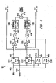
- FIGURE 6 shows one alternate embodiment 60, the need for which arises because of the fact that some commonly used high-speed logic technologies, such as differential current mode logic (CML), are not amenable to 3-input gates.
- CML differential current mode logic
- a 3-input function needs to be implemented as a cascade of two 2-input functions.
- a straightforward implementation of this concept would convert each 3-input gate to a cascade of two 2-input gates, resulting in a total of eight 2-input gates replacing the original four 3-input gates.
- FIGURE 6 shows a more efficient implementation using just two 2-input AND gates 617 and 618 (U3 and U4) and two exclusive-OR gates 615 and 616 (U1 and U2).
- Circuit 60 is logically equivalent to circuit 10 (FIGURE 1). In this case, there are only two output gates for the phase output. As with circuit 10, all logic of circuit 60 operates at half rate or less.
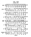
- FIGURE 7 shows the timing diagram for circuit 60.
- the theory of operation is best explained by describing operation with a pattern of alternating 0's and 1's (ie 01017) first, then describing what happens for other patterns.
- a 0101... pattern one flip-flop 611 or 612 will always sample 0's and the other flip-flop will always sample 1's.
- a 0101... pattern is received by the phase detector with timing such that output 602 of FF1 611 is always 0 and output 603 of FF2 612 is always 1.
- gate U 1 615 is effectively reduced to a non-inverting buffer and gate U2 616 is effectively reduced to an inverter.
- gates U3 617 and U4 618 driven by delayed clock 605 (delayed by 614) and its complement and unretimed data 606 and its complement 607 is then the same as for circuit 10.
- Output 608 of gate U3 617 contains pulses that begin on a positive data transition and end on a negative clock transition.
- output 609 of gate U4 618 contains pulses that begin on a negative data transition and end on a positive clock transition.
- Gates U3 617 and U4 618 pulse alternately in time and are summed by combiner 619 resulting in phase output 610. The pulse duration depends on the time interval between data and clock, as was the case with circuit 10.
- output 609 of gate U4 When the delayed clock 605 goes high, output 609 of gate U4 will go low, ending an output pulse. Additionally, output 602 of FF1 611 will go high, which will disable gate U3 617 via gate U1 615, preventing it from initiating an extra output pulse.
- timing-margins basically also applies to timing-margins with respect to FIGURE 7 of circuit 60, except for the time delays.
- ⁇ for both unretimed data 600 and clock 601, there are now individually chosen delays, ⁇ d and ⁇ c , respectively with respect to circuits 613 and 614.
- ⁇ d is the same as ⁇ in circuit 10.
- ⁇ c is equal to ⁇ plus the propagation delay of an exclusive-OR gate, to make up for the delay through gates U1 615 and U2 616.
- FIGURE 8 shows critical timing relationships, using correct values of ⁇ d and ⁇ c , for the worse case of 0.4 UI late clock phase.
- the output pulse width is still independent of small variations (up to 1 ⁇ 2 UI) in the flip-flop propagation delay, and is immune to flip-flop jitter.
- the reference points A, B, C, D and E are, with respect to FIGURE 6, and ⁇ c , is 0.5UI+flip-flop delay and ⁇ d is 0.5UI+flip-flop delay + exclusive OR delay.
- the minimum flip-flop timing margin with respect to the leading edge of an output pulse is .6 UI.
- the minimum flip-flop timing margin with respect to the trailing edge of an output pulse is 1 ⁇ 2 UI.
- any number and combination of other logical elements such as AND gates, OR gates, XOR gates, or other elements, such as, for example, flip-flops, retimers and latches, can be used to generate consecutive pulses which are not generated by the same hardware (thus avoiding overlap or near-overlap) and which can be averaged over a number of signal pulses.
- Such alternative circuit configurations which can be arrived at by starting with the desired pulse output characteristics and working backward to achieve a properly functioning combination of elements, will allow circuit designers design freedom to match the actual circuit to specific design criterion or overall circuit limitations. This can become important if signal timing factors or signal propagation delays become critical.
Description
- This invention relates to phase detectors and more particularly to a system and method for clock recovery from non-return-to-zero (NRZ) data and even more particularly to such a system and method for an improved timing margin half-rate continuous phase detector.
- In data transmission systems using NRZ formatting, there is no explicit clock signal transmitted with the data that can be used to recover the data. The clock must first be recovered from the data, based on the time of the data transitions. This requires a phase detector which measures the phase error between the NRZ data and an internal clock, producing an error signal. The error signal drives a control loop that corrects the error. In a properly working system, the control loop will be able to hold the phase error to a negligible value. The recovered clock is then used to recover the data. A circuit which performs the above operations is called a clock/data recovery (CDR) circuit. Nearly all modern data transmission systems use CDR circuits and the phase detector is an essential part of such a CDR circuit.
- Two classes of phase detectors are in common use, commonly referred to as "bang-bang" and "continuous." The bang-bang circuits are derived from Alexander's original design, as discussed in Alexander, JDH, "Clock Recovery from Random Binary Signals," Electronic Letters, v. 11, n. 32, pp 541-542, Oct. 30, 1975. The bang-bang class has a binary quantized output that only indicates whether the clock is "early" or "late," but not by how much. This results in the control loop operating in a discontinuous or "bang-bang" mode, which adds spurious jitter to the recovered clock and thus argues against the use of bang-bang phase detectors in jitter measurement systems. Also, in communications systems, this spurious jitter reduces the performance of the system.
- The continuous phase detectors are patterned after, or emulate, Hogge's original design as discussed in Hogge, CP, "A Self Correcting Clock Recovery Circuit," Journal of Lightwave Technology, v. LT-3, n. 6, pp 1312-1314, Dec. 1985. These detectors have an output that can be used to generate a voltage proportional to phase error, thus resulting in a "proportional" mode for the control loop. This is much more desirable in operational systems and essential in jitter measurement systems. However, many systems operating at state-of-the-art clock rates still use bang-bang phase detectors because they will operate considerably faster than continuous phase detectors, for a given logic hardware technology. This is because the timing is more critical in the continuous phase detectors of known design.
- The phase detectors described above are clocked at "full rate," meaning that the clock frequency is equal to the baud rate of the data. For example, if the data is at a 10 Gbit/s rate (1010 baud), and the clock is 10 GHz, the circuit is described as being clocked at "full rate." In this context, "half rate" clocking would refer, for example, to 10 Gbit/s data with a 5 GHz clock.
- In an effort to get more speed, "half-rate" clocked continuous phase detectors have been developed as discussed by Reis, AD, et al, "High Date Rate Synchronizers Operating at Low Speed." KEGS 2001. 8th IEEE International Conference on Electronics, Circuits and Systems, 2001, pp 1127-1130, V3 and Savoj, J and Razavi, B, "Design of Half-Rate Clock and Data Recovery Circuits for Optical Communications Systems, IEEE Journal of Solid-State Circuits, V36, No, 5, May 2001, pp 761-768. The clock has two phases, 180° apart, which activate duplicate flip-flops. The 2 phases correspond to the rising and falling edges of the clock waveform. This modification, potentially at least, gives the flip-flops twice as much time to switch, and thus enables up to twice the maximum clock rate. However, these half-rate phase detectors still have limitations with respect to critical timing margins that limit their maximum clock rate. It should also be noted, that because of the analog nature of continuous phase detectors, their accuracy and dynamic range gradually deteriorate as the maximum rate is approached. Therefore, even below the maximum rate, increased design margin usually improves performance. These increased margins then effectively increase the maximum data rate. Accordingly, a need exists in the art for a half-rate continuous phase detector with improved timing margins for increased speed and performance. REIS A D; Rocha JF; GAMEIRO A S; CARVALHO J P; 'Heigh data rate synchronizers operating at low speed' ICECS 2001. 8TH IEEE INTERNATIONAL CONFERENCE ON ELECTRONICS, CIRCUITS AND SYSTEMS, vol. 3, 2-5 September 2001, pages 1127-1130, XP002267204 Malta describe a phase detector producing pulses representative of the phase difference between data pulses and local clock. Data signals, both retimed and unretimed are logically combined with clock signals and inverse clock signals using a plurality of logical gates.
- The present invention provides a circuitry for providing an output representative of input data signals and clock signals according to
claim 1. Preferred embodiments of the invention are defined in dependent claims. - The present invention is directed to a phase detector constructed from a plurality of multi-input gates which combine combinations of unretimed input data with retimed data and with clock signals to achieve output pulses proportional to the phase difference between the unretimed data and the clock.
- In the embodiment the phase detector comprises an input for receiving data signals; an input for receiving clock signals; an output for providing phase control signals; data retiming circuiting for accepting unretimed data signals from said data input and for providing even and odd retimed signals therefrom; a plurality of multi-input gates having inputs connected to different combinations of said unretimed data signals, said retimed data signals, and said clock signals, such that no said gate can be active in two consecutive UIs, when a UI is defined as the length of time allocated to a single bit; and a combiner for mixing the outputs of at least two of said gates.
- The forgoing has outlined rather broadly the features and technical advantages of the present invention in order that the detailed description of the invention that follows may be better understood. Additional features and advantages of the invention will be described hereinafter which form the subject of the claims of the invention. It should be appreciated by those skilled in the art that the conception and specific embodiment disclosed may be readily utilized as a basis for modifying or designing other structures for carrying out the same purposes of the present invention. It should also be realized by those skilled in the art that such equivalent constructions do not depart form the spirit and scope of the invention as set forth in the appended claims. The novel features which are believed to be characteristic of the invention, both as to its organization and method of operation, together with further objects and advantages will be better understood from the following description when considered in connection with the accompanying figures. It is to be expressly understood, however, that each of the figures is provided for the purpose of illustration and description only and is not intended as a definition of the limits of the present invention.
- For a more complete understanding of the present invention, reference is now made to the following descriptions taken in conjunction with the accompanying drawing, in which:
- FIGURE 1 shows one embodiment of an illustrative example of the invention;
- FIGURE 2 shows the embodiment of FIGURE 1 with the addition of a reference output;
- FIGURE 3A, 3B and 3C show timing diagrams for the circuit of FIGURE 1;
- FIGURE 4 shows timing diagrams of the circuit of FIGURE 1 for the situation where the rise and fall time of the output pulses is significant;
- FIGURE 5A shows a timing diagram of the circuit of FIGURE 1 with nominal clock phase and τ=.5UI+flip-flop delay;
- FIGURE 5B shows a timing diagram of the circuit of FIGURE 1 with a 0.4UI late clock phase and τ=.5UI+flip-flop delay;
- FIGURE 6 shows another embodiment of the invention;
- FIGURES 7 and 8 show timing diagrams of the circuit of FIGURE 6;
- FIGURE 9A, 9B and 9C show prior art timing diagrams for full-rate clock;
- FIGURES 10A, 10B, and 10C show prior art timing diagrams for half-rate clock;
- FIGURES 11A and 11B show prior art flip-flop timing;
- FIGURES 12A and 12B show prior art later timing;
- FIGURE 13 shows prior art master/slave flip-flip constructed from two latches;
- FIGURES 14A, 14B, and 14C show a prior art multiplexer and its timing;
- FIGURES 15A, 15B, and 15C show a prior art demultiplexer and its timing;
- FIGURES 16A, 16B, and 16C show a prior art half-rate retimer and its timing;
- FIGURES 17A, 17B, 17C and 17D show a prior art phase detector and its timing;
- FIGURES 18A and 18B show a prior art reference output and its timing;
- FIGURES 19A and 19B show a prior art half-rate phase detector and its timing;
- FIGURES 20A, 20B, 20C and 20D show a prior art half-rate phase detector and its timing.
- Before beginning the detailed description it may be helpful to discuss the ramifications of clock phase as it relates to the task of correctly recovering data. The discussion which follows are with reference to FIGURE 9A-20D, all of which are provided by way of background.
- Figures 9A, 9B and 9C are timing diagrams for full-rate operation showing
clock waveforms data sample time sample time - The data is normally captured by an edge-triggered D-type flip-flop, which can be thought of as a sampler that samples the data at the time of a positive going transition of the clock (903A, 903B, 903C). Thus the clock and data transitions should be spaced ½ UI apart.
- In actual systems, there is some dead time when the data is transitioning, and thus not yet valid. This reduces the timing margin below ½ UI, but the principle remains the same: the optimum time to sample the data is in the center of the time interval in which the data is valid.
- FIGURES 10A, 10B and 10C are similar to FIGURES 9A, 9B and 9C, except they show the half-rate clock operation. In this case,
data 1002A, 1002B, and 1002C are sampled at everyclock transition clock signal - Jitter refers to variation in the clock phase (the relationship of the clock signal to the data signal) from bit to bit. If clock phase is thought of statistically as a random variable, then jitter is a measure (similar to variance) of the "randomness" of the variable. While the clock phase may be correct on the average, it can vary considerably for any particular bit. If a jittery data signal is sampled at uniform intervals, instead of the sampling taking place in the middle of a bit, it will be early some of the time and late some of the time. This timing error makes the system more vulnerable to bit errors due to noise and other impairments.
- Another way of thinking of jitter is to consider clock phase to be a signal. Then jitter represents noise added to this phase signal. Jitter is closely related to "phase noise," which is a measure of spurious phase modulation of a sine wave.
- There are basically two sources of jitter. A straightforward jitter mechanism is that the clock signal itself has jitter on it, and the device generating the data will inherit this jitter. This jitter mechanism is independent of the characteristics of the data being transferred. A second jitter mechanism is called "data pattern jitter." In this case, the timing of data will be corrupted while passing through a data transfer device due to group delay impairments in the device, which occur even in the presence of a perfect clock. Its name derives from the fact that the characteristics of the jitter depend on the characteristics of the data being transferred.
- It is important to keep in mind that phase detectors are built from hierarchically organized combinations of circuit blocks, rather than as being an unrelated collections of gates and other elements.
- FIGURE 11A shows D flip-flop 1100 (henceforth referred to simply as a "flip-flop"), and FIGURE 11B shows its timing diagram. The basic function of flip-
flop 1100 is to take indata 1101 at the D input and send the data back out of the Q output tooutput lead 1102, under the control ofclock 1103. At positive clock transition 1104 (FIGURE 11B), if the D input is low, the output will go low 1105 (or stay low if it was already low). Similarly, if the D input is high at apositive clock transition negative clock edge 1109, the flip-flop does nothing. - A flip-flop can be thought of as a data retimer. Suppose the unretimed data at the D input to the flip-flop has a moderate amount of jitter on it. The flip-flop will, in general, sample the data at non-optimum times, but will still arrive at the correct value for each bit. It will then reproduce these bits at the output, however the timing of them will be controlled by the clock, not the time of arrival at the input. Thus a perfect flip-flop, with a perfect clock, will retime data so as to remove all jitter.
- Unfortunately, if the clock has jitter, the output will inherit this jitter. Also, if the flip-flop has frequency-dependent amplitude or group delay, the output will have pattern jitter. Therefore, in practice, a flip-flop may either increase or decrease jitter.
- For purposes of discussion herein, the input data to a flip-flop will be referred to as "unretimed data" and the output data from a flip-flop will be referred to as "retimed data".
- FIGURE 12A shows D latch 1200 (henceforth referred to simply as a "latch") and FIGURE 12B show its timing diagram. Latches are important in general because they are building blocks for flip-flops and specifically because they are used explicitly in the aforementioned Savoj et al paper. Like the flip-flop, the basic function of the flip-flop is to take in
data 1201 at the D input and send the data back out ofQ output 1202. However, the latch is controlled by alatch input 1203 instead of a clock input, and its behavior is slightly different than a flip-flop. It has two modes, depending on the state of the latch input. When the latch input is low 1204, the latch is in track mode. Track mode is a straight-through transfer mode, in which the output responds immediately to the input. When the latch input goes high, the latch goes to latch mode. In latch mode, the output is latched in whatever state it had upon leaving track mode. Eventually, the latch input transitions from high to low 1206, returning the latch to track mode. At the instant of this transition, the output state immediately changes (if necessary) to be the same as the current input state, and follows any input changes after that. - FIGURE 13 shows how flip-
flop 1300 can be constructed using twolatches 1200 and 1200' When made this way, it is called a master-slave flip-flop.Master latch 1200 operates fromclock input 1302 and slave latch 1200' operates from the complement (via inverter 1301) of the clock input. Therefore, when the clock is low, the master tracks and the slave latches. When the clock goes high, the master latches and the slave tracks. Operation is as follows: the master latch latches theunretimed data 1303 on positive clock transitions, and feeds it to the slave latch. The slave latch, currently in track mode, passes the data through to the output. On the next negative clock edge, the slave latches the data at the output to hold it. Meanwhile, the master latch begins to track the current state of the unretimed data. - Because each bit requires 2 operations of the master-slave flip-flop, each operation must take place in less than ½ of a clock period. If a full rate clock is used, ½ of a clock period is ½ UI. This requires the constituent latches to be able to operate at twice the data rate. If a half rate clock is used, ½ of a clock period is 1 UI. This merely requires the constituent latches to be able to operate at the data rate.
- A 1:2 demultiplexer (for the purposes of discussion herein) is a device that splits an unretimed data signal into two retimed output data signals, with the output data rate being half of the input data rate. Its basic function is to slow down data so that it can be processed at a lower rate by slower hardware.
- FIGURE 14A and 14B show how demultiplexer 1400 (FIGURE 14C) can be constructed from two flip-
flops 1300 and 1300'. A half-rate clock 1401 is used for one flip-flop, (denoted "even"), and the complement of that half-rate clock 1401' is used for the other flip-flop, (denoted "odd"). Flip-flop 1300 samples unretimeddata 1402 on positive going clock edges, while flip-flop 1300' samples unretimed data on negative going clock edges. The sampled data is at half the rate of the unretimed data. Retimed data is alternately transferred to "even"output 1403, then to "odd"output 1404. Thus, even numbered bits go to the even output and odd numbered bits go to the odd output. - A 2:1 multiplexer does the reverse operation by combining two half-rate data inputs into one full rate data input. FIGURES 15A and 15B show that 2:1 multiplexer 1500 (FIGURE 15C) is simply a data selector switch driven by a half-rate clock. When half-
rate clock 1501 is high, one input is switched through tooutput 1701; when the clock is low, the other input is switched through tooutput 1701. The complementary clock signals are generated byinverter 1703. The data switch is easily constructed using combinatorial logic. A multiplexer inherently retimes the data. - FIGURES 16A and 16B show that it is also possible to combine 1:2
demultiplexer 1400 with 2:1multiplexer 1500 to form half-rate retimer 1600, the symbol for which is shown in FIGURE 16C. The multiplexing function undoes the de-multiplexing function; the result is that the circuit merely retimes the data. Thus data in 1601 is retimed as data out 1603, as shown in FIGURE 16B. It performs essentially the same function in terms of retiming data as a flip-flop; the main difference is that it operates from half-rate clock 1602, and the internal operation of the retimer is at half the rate of the flip-flop. Thus, it potentially can operate at a higher speed. A half-rate retimer is sometimes referred to as a double-edge triggered flip-flop because it responds to both positive and negative clock edges. -
Circuit 1700 shown in FIGURE 17A, retimes the unretimed data with a conventional flip-flop 1200 (FIGURE 12), clocked at full rate byclock 1702. An exclusive-OR gate 1705 compares retimeddata 1703 tounretimed data 1701.Output 1704 of the gate consists of pulses with duration proportional to the phase ofclock 1702. A pulse is produced only when there is a data transition from which to gather phase information. For nominal clock phase, the pulses are ½ UI long, as shown by the pulses designated as 1706 in FIGURE 17B. When the clock is early, the pulses narrow as shown by the pulses designated as 1707 on FIGURE 17C. When the clock is late, the pulses widen, as shown by the pulses designated 1708 in FIGURE 17D. The pulses can be smoothed by a low pass filter to produce a voltage proportional to phase. -
Circuit 1700 has at least four serious limitations. (1). The flip-flop must operate at the full clock rate. (2). The effective data rate of the phase output is twice the data rate of the unretimed data. This immediately limits the maximum clock rate to half the maximum switching rate capability of the underlying logic technology. (3). When the phase deviates significantly from nominal in either direction, the phase output is called upon to put out extremely narrow width pulses. This constraint either limits the maximum usable phase range or further limits the maximum clock rate to even less than half of the maximum logic switching rate. (4). The circuit does not compare the unretimed data timing directly against the clock. Instead the unretimed data timing is compared against the retimed data at the output of the flip-flop. The retimed data serves as a proxy for the clock timing. Therefore, any jitter, propagation delay drift, or other inaccuracy inherent in the flip-flop degrades output accuracy. A significant, but often overlooked, source of error in flip-flops operating near their maximum rate is a dependence of propagation delay on the amount of set up time at the data input. - Since phase pulses are only produced at data transitions, the average value of the phase output depends on the average density of data transitions. Thus, the reference voltage representing zero phase error shifts according to the transition density. To counteract this problem,
circuit 1800, shown in FIGURE 18A adds an additional "reference"output 1805 that generates a shifting reference voltage that has the same dependency on data transition density, but is independent of phase. The reference output consists of pulses with fixed duration of ½ UI generated after each data transition. The reference output is subtracted from the phase output, resulting in a corrected output that is always zero (on the average) when the phase error is zero. The reference output, like the phase output, must operate at twice the rate of the unretimed data, which again limits the maximum clock rate. Also, the two flip-flops flop 1810 and set-up/hold time of second flip-flop 1811. FIGURE 18B shows the timing forcircuit 1800 with respect to data in 1801, clocks in 1802, Q1 1803,Q2 1804, and reference out 1805. The output from flip-flops gate 1806. -
Phase detector 1900 shown in FIGURE 19A, replaces the full-rate flip-flop with half-rate retimer 1600. The operation of exclusive-OR gate 1906 to generatepulses 1903 having duration proportional to phase is identical to that described with respect tocircuit 1700. Themajor advantage circuit 1900 overcircuit 1700 is that the retiming function is now done at half-rate, which addresses limitation (1) discussed above. Limitations (2) through (4) remain. FIGURE 19B shows the timing forcircuit 1900 with respect to data in 1901,clock 1902, data out 1903 and phase out 1904. - FIGURE 20A shows the phase detector described in the above-identified Savoj et al reference, and FIGURE 20B shows its timing diagram for optimum clock phase with respect to,
clock 2001, data in 2002,Y1 2003,X2 2005, phase out 2007,Y1 2004,Y2 2006 and reference out 2008. The circuit operates from half-rate clock 2001. It uses four latches 2010-2012 organized into a 1:2 demultiplexer using the architecture previously described. The multiplexer outputs supply the recovered data, which also drives exclusive-OR gate 2015 to producereference output pulses 2008. Note that these reference pulses are of 1 UI duration, in contrast tocircuit 1800 in which they are of ½ UI duration. In addition, the two master latch outputs are brought out separately to another exclusive-OR gate 2014 that produces thephase output pulses 2007. - Although the latches are clocked at half-rate, FIGURE 20B shows that the output of the
latches 2007 contains ½ UI duration pulses. These pulses must then propagate through exclusive-OR gate 2015. When the clock phase is early, as shown in FIGURE 20C, the pulse duration decreases to less than ½ UI. For large negative phase errors, the output pulse duration becomes impractically small, as shown bygraph 2007, FIGURE 20C and the output pulses are no longer accurately produced, resulting in phase detector measurement error. - When the clock phase is late, as shown in FIGURE 20D, the pulse duration increases to more than ½ UI. When there are consecutive output pulses, the gap between them decreases to less than ½ UI, as shown by
graph 2007 FIGURE 20D. This results in narrow negative going pulses. For large negative phase errors, the pulse duration becomes impractically small, and the output pulses are no longer accurately produced, again resulting in phase detector measurement error. In addition, in the late timing case, narrow pulses appear at nodes X1 and X2 (graphs - The reference output works in a somewhat different manner than the phase detector. The even demultiplexed data is compared to the odd demultiplexed data by a second exclusive-OR gate. The gate produces a 1 UI pulse after each data transition. When these pulses are averaged, they produce exactly twice the voltage as the reference pulses of
circuit 1800. Thus, in practice, this voltage is attenuated by a factor of 2 before being subtracted from the phase output. Because of the doubled pulse duration, the reference output actually attains the full benefit of the half-rate clocking. - The inventive concepts will now be described with respect to two embodiments, namely; a high performance embodiment, and an alternate embodiment, with lower performance.
- FIGURE 1 shows the schematic of a
first embodiment 10. As in phase detector 2000 (FIGURE 20A), the data recovery is done, for example, by a conventional half rate 1:2 demultiplexer, consisting of two flip-flops 111, 112 (FF1 and FF2) clocked on opposite clock edges ofclock signal 100. However, in this case, the master latch outputs are not broken out separately. Instead, retimeddata 102 is combined with delayed versions ofunretimed data 113 and delayed versions ofclock signal 105 by, in this embodiment, a bank of four 3-input ANDgates passive combiner 121 to formphase output 110. Note that in the drawing a "bubble" at the input of the AND gates denotes an inversion. Also note that all gates operate at half rate or less. - FIGURE 2 shows the addition of
XOR gate 1806 to generate a reference output as described with respect to FIGURE 18A. This gate (or other circuitry) may be conveniently added onto the circuit of FIGURE 1 to make a complete working system, since both designs are based on a 1:2 demultiplexer. - Before describing the operation of the
circuit 10, some definitions are necessary. Data bits that are valid during a positive clock edge are defined as "even" bits. Data bits that are valid during a negative clock edge are defined as "odd" bits. Data transitions that begin with an even bit and end with an odd bit are defined as "even transitions." Data transitions that begin with an odd bit and end with an even bit are defined as "odd transitions." Data transitions that begin with a 0 bit and end with a 1 bit are defined as "positive transitions." Data transitions that begin with a 1 bit and end with a 0 bit are defined as "negative transitions." - FIGURE 3A shows the timing diagram (optimum clock phase) for circuit 10 (without optional low pass filters 120). Similarly, figures 3B and 3C show the timing for late and early phase, respectively. To simplify the description, the delay τ through the flip-flop will be assumed to be zero. The effect of non-zero τ delay will be discussed hereinafter. As shown in FIGURE 1,
FF1 111 processes even data, andFF2 112 processes odd data. The retimed data (or complement thereof) is combined with the unretimed data (or complement thereof) and the clock (or complement thereof) in various combinations by AND gates 115-118 (U1-U4). - In the embodiment of FIGURE 1, gate U1 generates a pulse at each even, negative transition. Gate U2 generates a pulse at each even, positive transition. Gate U3 generates a pulse at each odd, negative transition and gate U4 generates a pulse at each odd, positive transition. The duration of the pulses from gates U1-U4 is proportional to phase. The pulses are optionally low pass filtered by
filter 120, then summed bylinear combiner 121, resulting in a phase output that consists of a pulse proportional to phase at every data transition.Phase signal 110 in FIGURES 3A, 3B, and 3C is for the case of nolow pass filter 120. The effect of a low pass filter will be discussed hereinafter. The output combining is explained in more detail below. This output is functionally the same as the outputs discussed above with respect to the prior art, and thuscircuit 10 is a direct replacement therefore. - The theory of operation is best explained by first describing operation with a sequence of alternating 0's and 1's (ie 01010...), then describing what happens for other sequences. With a 0101... pattern, one flip-
flop FF 1 is always 0 and FF2 is always 1. In this case, gates U1 and U4 will be disabled, and gates U2 and U3 will be effectively reduced to two input gates, driven by clock 100 (or its complement) and unretimed data 104 (or its complement). Gate U2 puts out pulses that begin on a positive data transition and end on a negative clock transition. Similarly, gate U3 puts out pulses that begin on a negative data transition and end on a positive clock transition. The U2 and U3 pulses alternate in time and are summed bycombiner 121. The pulse duration depends on the time interval between data and clock, which is proportional to phase. - With other sequences, there are always at least two 0's preceding a 1 and two 1's preceding a 0. Suppose two or more consecutive 0's have been received by
phase detector 10. Then bothFF 1 and FF2 will be low. In this case, gates U1 and U3 will be disabled, and gates U2 and U4 will be effectively reduced to two input gates. These gates will be enabled alternately one gate at a time by the clock and clock complement, which drive gates U2 and U4 respectively. Suppose the clock is low, hence gate U4 is enabled. When a 0 to 1 data transition occurs, gate U4 will go high, beginning an output pulse. When the clock goes high, gate U4 will go low, ending the output pulse. Additionally, FF1 will go high, which will disable gate U2, preventing it from initiating an additional output pulse - In practice, patterns are mixtures of 0101... sequences and other sequences. Figure 3A shows that the circuit is able to transition between these sequences correctly.
- No gate can be active during two consecutive UI's, because of the following mathematical properties: (1) positive and negative transitions always alternate (although there can be UI's in-between without transitions); (2) transitions occurring in consecutive UI's cannot both be even or both be odd. Therefore, any individual gate operates at half rate (or less), and always has at least 1 UI of dead time between pulses. Ideally, the outputs of gates U1-U4 could simply be combined by a four-input OR gate, (instead of the linear combiner actually used), to produce the phase output waveforms of FIGURES 3A-3C, since (ideally) only one gate is active at a time.
- When the phase approaches ½ UI late, the pulses at the outputs of gates U1-
U4 approach 1 UI in duration. In that case, when there are consecutive data transitions, there is very little time between the end of one pulse and the beginning of the next. In the idealized case shown in FIGURE 3B, the phase output would contain narrow negative going pulses representing the time between output pulses. In practice, for a system operating near the capability of the logic hardware, this pulse would probably be too narrow to reproduce, resulting in the phase output staying high for an excessive period of time. As described previously, this is a significant problem for prior art phase detectors. However, the concepts taught herein overcome this limitation by taking advantage of the fact that the phase detector output is averaged over many pulses before being utilized. Because of this averaging, which can be thought of integration, the only requirement on the phase detector for accuracy is that the area under the pulses correctly indicates the phase. If this constraint is met, it is not necessary for the phase detector to accurately reproduce the theoretically correct pulse shape. - To be more specific, the area under the curve of phase output voltage 110 (FIGURE 1) must be equal to the sum of the areas under the curves of individual gate outputs, 106, 107, 108, and 109.
Linear combiner 121 will always met this requirement because of the mathematical property that the integral of a sum equals the sum of the constituent integrals. If thecombiner 121 is passive, it is virtually guaranteed by design to be linear. Properly designed active combiners can also be linear. The bandwidth of the combiner would be dependent upon system usage and would typically be between 0-640 MHz when the system is operating at a data rule of 40 G bite/sec with a run length of 32 bits. - FIGURE 4 illustrates what happens when gate outputs 106, 107, 108, and 109 have non-zero rise and fall times. The pulses run together at
phase output 110. However, the area will be correct for the reasons given above. This would not be the case iflinear combiner 121 were replaced by a 4-input OR gate, since an OR gate is a non-linear device. An OR gate implementation would work over a reduced phase range and/or with reduced accuracy. - In some cases, there can be a problem with crosstalk between
gate outputs linear combiner 121. The optional low pass filters 120, FIGURE 1, can be used to prevent high speed transient pulses coming out of one gate from disrupting the operation of the other gates. These filters can either replace or supplement the low pass filters used downstream from the phase output. The presently contemplated range for the filter is 0-640 MHz. - The
τ delay reference plane 130, as shown in FIGURE 1. Therefore, ifdelay 114 is inserted in the clock and delay 113 is inserted in the unretimed data path, this delay has the same effect as if a hypothetical negative delay had been inserted at the flip-flop outputs. This negative delay can be used to effectively cancel out the propagation delay of the flip-flops. Second, by adding an additional delay of ½ UI beyond the flip-flop delay, the timing margin is increased. - FIGURE 5A illustrates this situation for
gate U1 115, which is representative of the other three phase output gates, with nominal clock phase.Output 106 and the three inputs (102, 104, 105), of this gate are shown. For illustrative purposes, the complement 104' of the delayedunretimed data 104 is displayed, to take into account the inversion bubble at the input toU1 115. Delayedclock 105 is also shown. FIGURE 5A assumes that τ is exactly ½ UI longer than the propagation delay of flip-flop 101. Output 106 (U1) of the AND gate goes high if, and only if, all three inputs (102, 104', and 105) are high. - For the nominal phase case of FIGURE 5A, the minimum flip-flop timing margin with respect to the leading edge of an output pulse is 1 UI. For example,
pulse 505 begins at t=5.5 and ends at t=6.0. It is necessary for the output ofFF 1 102 to be high during thepulse 505. It can be seen thatFF1 102 goes high at t=4.5 503, which is 1 UI earlier than necessary.FF1 102 then stays high for many UIs after the end of the pulse at t=5.5. Similarly, the minimum flip-flop timing margin with respect to the trailing edge of an output pulse is ½ UI. For example,pulse 507 begins at t=9.5 and ends at t=10. It is necessary for the output ofFF1 102 to be high during thepulse 507. It can be seen thatFF1 102 stays high until t=10.5 504, which is 1/2 UI later than necessary.FF1 102 had also been high for many UI before the beginning of the pulse at t=9.5. - FIGURE 5B shows how the waveforms change when the clock phase is .4 UI late. The output pulses (505', 506' and 507') are now .9 UI long. The minimum flip-flop timing margin with respect to the leading edge of an output pulse has been reduced to .6 UI. For example, pulse 505' begins at t=5.5 and ends at t=6.4. The
output 102 ofFF1 111 goes high at t=4.9 503', which is .6 UI earlier than necessary. Theoutput 102 ofFF1 111 then stays high for many UI after the end of the pulse at t=6.4. Similarly, the minimum flip-flop timing margin with respect to the trailing edge of an output pulse is ½ UI. For example, pulse 507' begins at t=9.5 and ends at t=10.4. It is necessary for theoutput 102 ofFF1 111 to be high during pulse 507'. It can be seen thatoutput 102 ofFF1 111 stays high until t=10.9 504', which is ½ UI later than necessary. Theoutput 102 ofFF1 111 had also been high for many UI before the beginning of the pulse at t=9.5 - Since the accuracy of the phase detector is independent of flip-flop propagation delay, it will also be independent of pattern jitter caused by the flip-flops. This is an important consideration when the application is jitter measurement.
- If the phase detector is to be used at multiple clock rates, the conversion from UI to absolute seconds is made on the basis of the maximum data rate to be used. It is not necessary to increase τ at rates below the maximum. The circuit will work at least as well at lower rates as it does at the maximum, if the value of τ is chosen based on the maximum rate.
- FIGURE 6 shows one
alternate embodiment 60, the need for which arises because of the fact that some commonly used high-speed logic technologies, such as differential current mode logic (CML), are not amenable to 3-input gates. In technologies such as these, a 3-input function needs to be implemented as a cascade of two 2-input functions. A straightforward implementation of this concept would convert each 3-input gate to a cascade of two 2-input gates, resulting in a total of eight 2-input gates replacing the original four 3-input gates. However, FIGURE 6 shows a more efficient implementation using just two 2-input ANDgates 617 and 618 (U3 and U4) and two exclusive-OR gates 615 and 616 (U1 and U2).Circuit 60 is logically equivalent to circuit 10 (FIGURE 1). In this case, there are only two output gates for the phase output. As withcircuit 10, all logic ofcircuit 60 operates at half rate or less. - FIGURE 7 shows the timing diagram for
circuit 60. As withcircuit 10, the theory of operation is best explained by describing operation with a pattern of alternating 0's and 1's (ie 0101...) first, then describing what happens for other patterns. With a 0101... pattern, one flip-flop output 602 ofFF1 611 is always 0 andoutput 603 ofFF2 612 is always 1. In this case,gate U 1 615 is effectively reduced to a non-inverting buffer andgate U2 616 is effectively reduced to an inverter. The operation ofgates U3 617 andU4 618 driven by delayed clock 605 (delayed by 614) and its complement andunretimed data 606 and itscomplement 607 is then the same as forcircuit 10.Output 608 ofgate U3 617 contains pulses that begin on a positive data transition and end on a negative clock transition. Similarly,output 609 ofgate U4 618 contains pulses that begin on a negative data transition and end on a positive clock transition.Gates U3 617 andU4 618 pulse alternately in time and are summed bycombiner 619 resulting inphase output 610. The pulse duration depends on the time interval between data and clock, as was the case withcircuit 10. - With other patterns, there are always at least two 0's preceding a 1 and two 1's preceding a 0. Suppose two or more consecutive 0's have been received by
phase detector 60. Thenoutput 602 ofFF 1 611 andoutput 603 of FF2 will be low. In this case,gates U1 615 andU2 616 will be effectively reduced to non-inverting buffers.Gates U3 617 andU4 618 will be enabled alternately for one UI at a time by the clock signal and clock complement. Suppose the delayedclock 605 is low, hencegate U4 618 is enabled. When a 0 to 1 transition occurs in the delayedunretimed data 604,output 609 of gate U4 will go high, beginning an output pulse. When the delayedclock 605 goes high,output 609 of gate U4 will go low, ending an output pulse. Additionally,output 602 ofFF1 611 will go high, which will disablegate U3 617 viagate U1 615, preventing it from initiating an extra output pulse. - The discussion of timing-margins, regarding
circuit 10 basically also applies to timing-margins with respect to FIGURE 7 ofcircuit 60, except for the time delays. Instead of the same delay, τ, for bothunretimed data 600 andclock 601, there are now individually chosen delays, τd and τc, respectively with respect tocircuits circuit 10. However, τc is equal to τ plus the propagation delay of an exclusive-OR gate, to make up for the delay throughgates U1 615 andU2 616. - FIGURE 8 shows critical timing relationships, using correct values of τd and τc, for the worse case of 0.4 UI late clock phase. The output pulse width is still independent of small variations (up to ½ UI) in the flip-flop propagation delay, and is immune to flip-flop jitter.
- In FIGURE 8, the reference points A, B, C, D and E are, with respect to FIGURE 6, and τc, is 0.5UI+flip-flop delay and τd is 0.5UI+flip-flop delay + exclusive OR delay. Following along the lines of
circuit 10, the minimum flip-flop timing margin with respect to the leading edge of an output pulse is .6 UI. For example,output pulse 804 atpoint E 608 begins at t=5.5 and ends at t=6.4. Theoutput 602 ofFF1 611 at point A goes to createpulse 801 high at t=4.9, which is .6 UI earlier than necessary.Pulse 801 then stays high for many UI after the end of the pulse at t=6.4. Similarly, the minimum flip-flop timing margin with respect to the trailing edge of an output pulse is ½ UI. For example, pulse 802 begins at t=9.5 and ends at t=10.4. It is necessary forpulse 801 to be high during the 802 pulse. It can be seen that theoutput 602 of FF1 611 (pulse 801) stays high until t=10.9, which is ½ UI later than necessary.Pulse 801 had also been high for many UIs before the beginning of pulse 802 at t=9.5. - Note that
reference output 1805 described with respect tocircuit 10 can easily be added tocircuit 60 as discussed above. - It should be noted that because of the division of labor of the output gates, it is possible to utilize them individually, or in various pairs, rather than summing all their outputs together. For example, it may be desirable to have available the phase error of the positive transitions separately from the negative transitions. This would be important, by way of example, if there are asymmetrical impairments that affect one polarity more than another. Similarly, it may be desirable to have available the phase error of the even transitions separately from the odd transitions. If the data is generated by multiplexing up, as is usually the case, there could easily be systematic phase differences between even and odd data.
- It is also possible to simplify the circuit by building only a subset of the circuitry and recovering the clock from a subset of the transitions. In this case the assumption would be that the positive transitions only, or even transitions only, etc. are sufficiently representative of all transitions.
- Although the present invention and its advantages have been described in detail, it should be understood that various changes, substitutions and alterations can be made herein without departing from the spirit and scope of the invention as defined by the appended claims. Moreover, the scope of the present application is not intended to be limited to the particular embodiments of the process, machine, manufacture, composition of matter, means, methods and steps described in the specification. For example, while two embodiments (FIGURES 1 and 6) have been shown which allow for the logical combination of data input, retimed data signals and clock signals any number and combination of other logical elements, such as AND gates, OR gates, XOR gates, or other elements, such as, for example, flip-flops, retimers and latches, can be used to generate consecutive pulses which are not generated by the same hardware (thus avoiding overlap or near-overlap) and which can be averaged over a number of signal pulses. Such alternative circuit configurations, which can be arrived at by starting with the desired pulse output characteristics and working backward to achieve a properly functioning combination of elements, will allow circuit designers design freedom to match the actual circuit to specific design criterion or overall circuit limitations. This can become important if signal timing factors or signal propagation delays become critical.
- As one of skilled in the art will readily appreciate from the disclosure of the present invention, processes, machines, manufacture, compositions of matter, means, methods, or steps, presently existing or later to be developed that perform substantially the same function or achieve substantially the same result as the corresponding embodiments described herein may be utilized according to the present invention. Accordingly, the appended claims are intended to include within their scope such processes, machines, manufacture, compositions of matter, means, methods, or steps.
Claims (11)
- Circuitry (10, 60) for providing an output (1.10, 610) representative of a phase difference between input data signals (101; 601) and clock signals (100; 600), wherein the input data signals (101; 601) comprise even input data signals that are valid during a positive clock edge and odd input data signals that are valid during a negative clock edge, said circuitry comprising:means for separately retiming even and odd ones of said input data signals so as to provide even retimed data signals and odd retimed data signals;means (115, 116, 117, 118, 615, 616, 617, 618) for logically combining each of said retimed even and odd data signals with said data signals and with said clock signals; andmeans (121; 619) for combining said last-mentioned logically combined signals to provide said output.
- The circuitry of claim 1, wherein said logically combining means (615, 616, 617, 618) are adapted for logically combining each of said even retimed data signals with said data signals and said clock signals and each of said odd retimed data signals with said data signals and the inverse of said clock signals.
- The circuitry (10) of claim 1, wherein said logically combining means (115, 116, 117, 118) are adapted for logically combining each of said even retimed data signals with the inverse of said data signals and said clock signals and each of said odd retimed data signals with the inverse of said data signals and the inverse of said clock signals.
- The circuitry of one of the preceding claims wherein said last-mentioned combining means (121, 619) is a linear combiner.
- The circuitry (10) of claim 3 wherein said logically combining means comprise at least four, three-input AND gates whereby:a first input of a first gate (115) and a first input of a third gate (117) are said unretimed data signals (104) that have been inverted;a second input of said first gate is said even retimed data signal (102);a second input of a second gate (116) is said even retimed data signal inverted;a third input of said first gate is said clock signal (105);a first input of said second gate and a first input of a fourth gate (118) is said unretimed data signal;a second input of said third gate is said odd retimed data signal (103);a second input of said fourth gate is said odd retimed data signal inverted; anda third input of said third gate and a third input of said fourth gate is said clock signal inverted.
- The circuitry (10) of claim 5 wherein said gates comprise at least two, two-input AND gates (617, 618) and at least two two-input exclusive OR gates (615, 616) whereby:a first input of a first exclusive OR gate is said even retimed data signals (602);a second input of said first exclusive OR gate and a first input of a second OR gate is said unretimed data signals (604);a second input of said second exclusive OR gate is said odd retimed data signals (603);a first input to a first AND gate is the output (606) of said first exclusive OR gate;a second input to said first AND gate is said clock signal (605);a first input to a second AND gate is the output (607) of said second exclusive OR gate; anda second input to said second AND gate is said clock signal inverted.
- The circuitry (10) of claim 6 wherein said data signals (601) are delayed an amount τ1 (613) to compensate for signal delay through said retiming circuit (611, 612) and said clock signals (600) are delayed an amount τ2 (614) to compensate for signal delay through said retiming circuit and said exclusive OR gates (615, 616).
- The circuitry of one of the preceding claims further comprising:at least one low-pass filter (120) interposed between said logically combined signals (608, 609) and said combining means (619).
- A phase detector (10; 60) comprising:an input (101; 601) for receiving data signals;an input (100; 600) for receiving clock signals; andcircuitry (111, 112;611, 612)according to one of the preceding claims, wherein said means for logically combining comprises:a plurality of multi-input gates (115, 116, 117, 118; 615, 616, 617, 618), said gate inputs arranged in conjunction with different combinations of data signals retimed by said retiming circuitry, with unretimed data signals, with clock signals received from said clock input; and with the inverse of said clock signals, such that the linearly combined output (110; 610) of said gates is a signal at said output for providing pulses proportional to the phase difference between said data pulses received at said data input and clock pulses received said clock input.
- The phase detector (10; 60) of claim 9 further comprises:delay circuitry (113, 114; 613, 614) for delaying said unretimed data signals (101; 601) prior to said unretimed data signals arriving at said gate inputs.
- The circuitry of one of claims 1-3, wherein said means for logically combining comprises:a plurality of logic elements (115, 116, 117, 118; 615, 616, 617, 618) for combining combinations of said data signals, retimed data signals and clock signals, to provide a series of pulses indicative of said phase difference, said combination combined such that consecutive pulses are not generated by the same logic element; and comprising a combiner (619) for averaging said series of pulses over a plurality of data signal pulses.
Applications Claiming Priority (2)
| Application Number | Priority Date | Filing Date | Title |
|---|---|---|---|
| US10/268,196 US6686777B1 (en) | 2002-10-09 | 2002-10-09 | Phase detector having improved timing margins |
| US268196 | 2002-10-09 |
Publications (2)
| Publication Number | Publication Date |
|---|---|
| EP1408643A1 EP1408643A1 (en) | 2004-04-14 |
| EP1408643B1 true EP1408643B1 (en) | 2007-12-19 |
Family
ID=30443855
Family Applications (1)
| Application Number | Title | Priority Date | Filing Date |
|---|---|---|---|
| EP03011844A Expired - Fee Related EP1408643B1 (en) | 2002-10-09 | 2003-05-26 | Phase detector having improved timing margins |
Country Status (5)
| Country | Link |
|---|---|
| US (1) | US6686777B1 (en) |
| EP (1) | EP1408643B1 (en) |
| JP (1) | JP2004135318A (en) |
| CN (1) | CN100504403C (en) |
| DE (1) | DE60318162T2 (en) |
Families Citing this family (14)
| Publication number | Priority date | Publication date | Assignee | Title |
|---|---|---|---|---|
| US6956923B1 (en) * | 2003-01-17 | 2005-10-18 | Xilinx, Inc. | High speed phase detector architecture |
| US7505541B1 (en) * | 2003-01-17 | 2009-03-17 | Xilinx, Inc. | NRZ/PAM-4/PRML triple mode phase and data detector |
| US7805083B2 (en) * | 2003-04-28 | 2010-09-28 | Alcatel-Lucent Usa Inc. | Method and apparatus for data recovery in an optical transmission system |
| US7057435B2 (en) * | 2003-05-30 | 2006-06-06 | Regents Of The University Of California | Distributed delay-locked-based clock and data recovery systems |
| KR100479309B1 (en) * | 2003-07-26 | 2005-03-28 | 삼성전자주식회사 | Method for detecting phase difference, and apparatus for performing the same |
| US7049869B2 (en) * | 2003-09-02 | 2006-05-23 | Gennum Corporation | Adaptive lock position circuit |
| CN1937605B (en) * | 2005-09-19 | 2010-12-01 | 中兴通讯股份有限公司 | Phase position obtaining device |
| US7873132B2 (en) * | 2005-09-21 | 2011-01-18 | Hewlett-Packard Development Company, L.P. | Clock recovery |
| KR100656464B1 (en) * | 2005-12-28 | 2006-12-11 | 주식회사 하이닉스반도체 | Apparatus and method for generating output enable signal of semiconductor memory |
| US20080056403A1 (en) * | 2006-09-01 | 2008-03-06 | On Demand Microelectronics | Method and apparatus for timing recovery of pam signals |
| US8019022B2 (en) * | 2007-03-22 | 2011-09-13 | Mediatek Inc. | Jitter-tolerance-enhanced CDR using a GDCO-based phase detector |
| JP5148398B2 (en) * | 2008-07-23 | 2013-02-20 | アンリツ株式会社 | Demultiplexer |
| TWI555338B (en) * | 2014-11-14 | 2016-10-21 | 円星科技股份有限公司 | Phase detector and associated phase detecting method |
| US11212074B2 (en) | 2017-09-11 | 2021-12-28 | Sony Semiconductor Solutions Corporation | Data reception device and data transmission/reception device |
Family Cites Families (3)
| Publication number | Priority date | Publication date | Assignee | Title |
|---|---|---|---|---|
| US5719508A (en) * | 1996-02-01 | 1998-02-17 | Northern Telecom, Ltd. | Loss of lock detector for master timing generator |
| CA2201695C (en) * | 1997-04-03 | 2004-08-10 | Gennum Corporation | Phase detector for high speed clock recovery from random binary signals |
| US6483871B1 (en) * | 1998-12-28 | 2002-11-19 | Nortel Networks Limited | Phase detector with adjustable set point |
-
2002
- 2002-10-09 US US10/268,196 patent/US6686777B1/en not_active Expired - Lifetime
-
2003
- 2003-05-26 EP EP03011844A patent/EP1408643B1/en not_active Expired - Fee Related
- 2003-05-26 DE DE60318162T patent/DE60318162T2/en not_active Expired - Fee Related
- 2003-07-18 CN CNB031459978A patent/CN100504403C/en not_active Expired - Fee Related
- 2003-09-16 JP JP2003323294A patent/JP2004135318A/en not_active Withdrawn
Also Published As
| Publication number | Publication date |
|---|---|
| CN1488947A (en) | 2004-04-14 |
| US6686777B1 (en) | 2004-02-03 |
| JP2004135318A (en) | 2004-04-30 |
| EP1408643A1 (en) | 2004-04-14 |
| CN100504403C (en) | 2009-06-24 |
| DE60318162T2 (en) | 2008-12-04 |
| DE60318162D1 (en) | 2008-01-31 |
Similar Documents
| Publication | Publication Date | Title |
|---|---|---|
| EP1408643B1 (en) | Phase detector having improved timing margins | |
| US5329559A (en) | Phase detector for very high frequency clock and data recovery circuits | |
| US7587012B2 (en) | Dual loop clock recovery circuit | |
| KR101301698B1 (en) | Linear phase detector and clock & data recovery circuit including thereof | |
| US5374860A (en) | Multi-tap digital delay line | |
| US7251573B2 (en) | Phase detector | |
| EP1016218B1 (en) | Phase detector for high speed clock recovery from random binary signals | |
| US7450677B2 (en) | Clock and data recovery apparatus and method thereof | |
| US20080152057A1 (en) | Data Recovery Using Data Eye Tracking | |
| US8315349B2 (en) | Bang-bang phase detector with sub-rate clock | |
| US8023605B2 (en) | Oversampling circuit and oversampling method | |
| CN112703676A (en) | Frequency/phase lock detector for clock and data recovery circuit | |
| US20040114702A1 (en) | Bang-bang phase detector for full-rate and half-rate schemes clock and data recovery and method therefor | |
| KR100513385B1 (en) | Apparatus for recovering clock and data using linear phase detector, and method using the same | |
| KR100261294B1 (en) | High speed nrz data recovery apparatus | |
| US20060062339A1 (en) | Linear half-rate clock and data recovery (CDR) circuit | |
| KR100324981B1 (en) | Single terminal pulse gating circuit | |
| US7760030B2 (en) | Phase detection circuit and method thereof and clock recovery circuit and method thereof | |
| US7233187B2 (en) | Dual-mode pulse generator | |
| US7103131B1 (en) | System and method for half-rate clock phase detection | |
| US7127021B2 (en) | Interleaved pulse-extended phase detector | |
| Seedher et al. | Fractional rate phase detectors for clock and data recovery | |
| Golbus | Design of a 160 mW, 1 Gigabit/second, serial I/O link | |
| Elrabaa | Development of Digital Circuit Techniques for Clock Recovery and Data Re-Timing for High Speed Non-Return-to-Zero Source-Synchronous Serial Data Communications |
Legal Events
| Date | Code | Title | Description |
|---|---|---|---|
| PUAI | Public reference made under article 153(3) epc to a published international application that has entered the european phase |
Free format text: ORIGINAL CODE: 0009012 |
|
| AK | Designated contracting states |
Kind code of ref document: A1 Designated state(s): AT BE BG CH CY CZ DE DK EE ES FI FR GB GR HU IE IT LI LU MC NL PT RO SE SI SK TR |
|
| AX | Request for extension of the european patent |
Extension state: AL LT LV MK |
|
| 17P | Request for examination filed |
Effective date: 20040917 |
|
| AKX | Designation fees paid |
Designated state(s): DE FR GB |
|
| 17Q | First examination report despatched |
Effective date: 20041217 |
|
| RAP1 | Party data changed (applicant data changed or rights of an application transferred) |
Owner name: AVAGO TECHNOLOGIES GENERAL IP (SINGAPORE) PTE. LTD |
|
| GRAP | Despatch of communication of intention to grant a patent |
Free format text: ORIGINAL CODE: EPIDOSNIGR1 |
|
| GRAS | Grant fee paid |
Free format text: ORIGINAL CODE: EPIDOSNIGR3 |
|
| GRAA | (expected) grant |
Free format text: ORIGINAL CODE: 0009210 |
|
| AK | Designated contracting states |
Kind code of ref document: B1 Designated state(s): DE FR GB |
|
| REG | Reference to a national code |
Ref country code: GB Ref legal event code: FG4D |
|
| REF | Corresponds to: |
Ref document number: 60318162 Country of ref document: DE Date of ref document: 20080131 Kind code of ref document: P |
|
| EN | Fr: translation not filed | ||
| PLBE | No opposition filed within time limit |
Free format text: ORIGINAL CODE: 0009261 |
|
| STAA | Information on the status of an ep patent application or granted ep patent |
Free format text: STATUS: NO OPPOSITION FILED WITHIN TIME LIMIT |
|
| 26N | No opposition filed |
Effective date: 20080922 |
|
| PG25 | Lapsed in a contracting state [announced via postgrant information from national office to epo] |
Ref country code: FR Free format text: LAPSE BECAUSE OF FAILURE TO SUBMIT A TRANSLATION OF THE DESCRIPTION OR TO PAY THE FEE WITHIN THE PRESCRIBED TIME-LIMIT Effective date: 20081010 |
|
| PGFP | Annual fee paid to national office [announced via postgrant information from national office to epo] |
Ref country code: DE Payment date: 20090527 Year of fee payment: 7 |
|
| PGFP | Annual fee paid to national office [announced via postgrant information from national office to epo] |
Ref country code: GB Payment date: 20090520 Year of fee payment: 7 |
|
| GBPC | Gb: european patent ceased through non-payment of renewal fee |
Effective date: 20100526 |
|
| PG25 | Lapsed in a contracting state [announced via postgrant information from national office to epo] |
Ref country code: DE Free format text: LAPSE BECAUSE OF NON-PAYMENT OF DUE FEES Effective date: 20101201 |
|
| PG25 | Lapsed in a contracting state [announced via postgrant information from national office to epo] |
Ref country code: GB Free format text: LAPSE BECAUSE OF NON-PAYMENT OF DUE FEES Effective date: 20100526 |