EP1412550B1 - Support with getter-material for micromechanical device - Google Patents
Support with getter-material for micromechanical device Download PDFInfo
- Publication number
- EP1412550B1 EP1412550B1 EP02755628A EP02755628A EP1412550B1 EP 1412550 B1 EP1412550 B1 EP 1412550B1 EP 02755628 A EP02755628 A EP 02755628A EP 02755628 A EP02755628 A EP 02755628A EP 1412550 B1 EP1412550 B1 EP 1412550B1
- Authority
- EP
- European Patent Office
- Prior art keywords
- support
- support according
- gas absorbing
- base
- getter
- Prior art date
- Legal status (The legal status is an assumption and is not a legal conclusion. Google has not performed a legal analysis and makes no representation as to the accuracy of the status listed.)
- Expired - Lifetime
Links
- 239000000463 material Substances 0.000 title claims abstract description 44
- 238000004519 manufacturing process Methods 0.000 claims abstract description 20
- 239000011358 absorbing material Substances 0.000 claims description 23
- 239000002585 base Substances 0.000 claims description 18
- 229910052710 silicon Inorganic materials 0.000 claims description 12
- 239000010703 silicon Substances 0.000 claims description 12
- 229910045601 alloy Inorganic materials 0.000 claims description 11
- 239000000956 alloy Substances 0.000 claims description 11
- 229910052751 metal Inorganic materials 0.000 claims description 9
- 239000002184 metal Substances 0.000 claims description 9
- 239000000203 mixture Substances 0.000 claims description 9
- 229910052784 alkaline earth metal Inorganic materials 0.000 claims description 8
- 229910052742 iron Inorganic materials 0.000 claims description 6
- RTAQQCXQSZGOHL-UHFFFAOYSA-N Titanium Chemical compound [Ti] RTAQQCXQSZGOHL-UHFFFAOYSA-N 0.000 claims description 5
- 150000002739 metals Chemical class 0.000 claims description 5
- 229910052719 titanium Inorganic materials 0.000 claims description 5
- 239000010936 titanium Substances 0.000 claims description 5
- 229910052720 vanadium Inorganic materials 0.000 claims description 5
- 229910052726 zirconium Inorganic materials 0.000 claims description 5
- 239000003513 alkali Substances 0.000 claims description 4
- 150000001342 alkaline earth metals Chemical class 0.000 claims description 4
- 229910052782 aluminium Inorganic materials 0.000 claims description 4
- 229910052746 lanthanum Inorganic materials 0.000 claims description 4
- 229910052727 yttrium Inorganic materials 0.000 claims description 4
- QCWXUUIWCKQGHC-UHFFFAOYSA-N Zirconium Chemical compound [Zr] QCWXUUIWCKQGHC-UHFFFAOYSA-N 0.000 claims description 3
- ODINCKMPIJJUCX-UHFFFAOYSA-N calcium oxide Inorganic materials [Ca]=O ODINCKMPIJJUCX-UHFFFAOYSA-N 0.000 claims description 3
- 239000000292 calcium oxide Substances 0.000 claims description 3
- 239000000919 ceramic Substances 0.000 claims description 3
- 230000006870 function Effects 0.000 claims description 3
- 229910052758 niobium Inorganic materials 0.000 claims description 3
- 229910052761 rare earth metal Inorganic materials 0.000 claims description 3
- 239000004065 semiconductor Substances 0.000 claims description 3
- 229910052715 tantalum Inorganic materials 0.000 claims description 3
- BRPQOXSCLDDYGP-UHFFFAOYSA-N calcium oxide Chemical compound [O-2].[Ca+2] BRPQOXSCLDDYGP-UHFFFAOYSA-N 0.000 claims description 2
- 229910052804 chromium Inorganic materials 0.000 claims description 2
- 239000011521 glass Substances 0.000 claims description 2
- FZLIPJUXYLNCLC-UHFFFAOYSA-N lanthanum atom Chemical compound [La] FZLIPJUXYLNCLC-UHFFFAOYSA-N 0.000 claims description 2
- 229910052748 manganese Inorganic materials 0.000 claims description 2
- 229910052759 nickel Inorganic materials 0.000 claims description 2
- 150000002910 rare earth metals Chemical class 0.000 claims description 2
- VWQVUPCCIRVNHF-UHFFFAOYSA-N yttrium atom Chemical compound [Y] VWQVUPCCIRVNHF-UHFFFAOYSA-N 0.000 claims description 2
- 238000000034 method Methods 0.000 abstract description 13
- 238000004377 microelectronic Methods 0.000 abstract description 5
- 238000010521 absorption reaction Methods 0.000 abstract description 4
- 239000000356 contaminant Substances 0.000 abstract 5
- 239000007789 gas Substances 0.000 description 32
- 239000007787 solid Substances 0.000 description 15
- XUIMIQQOPSSXEZ-UHFFFAOYSA-N Silicon Chemical compound [Si] XUIMIQQOPSSXEZ-UHFFFAOYSA-N 0.000 description 10
- 238000000151 deposition Methods 0.000 description 10
- 230000008021 deposition Effects 0.000 description 9
- 230000005855 radiation Effects 0.000 description 5
- 239000011347 resin Substances 0.000 description 5
- 229920005989 resin Polymers 0.000 description 5
- XKRFYHLGVUSROY-UHFFFAOYSA-N Argon Chemical compound [Ar] XKRFYHLGVUSROY-UHFFFAOYSA-N 0.000 description 4
- IJGRMHOSHXDMSA-UHFFFAOYSA-N Atomic nitrogen Chemical compound N#N IJGRMHOSHXDMSA-UHFFFAOYSA-N 0.000 description 4
- 235000012431 wafers Nutrition 0.000 description 4
- 239000001257 hydrogen Substances 0.000 description 3
- 229910052739 hydrogen Inorganic materials 0.000 description 3
- 125000004435 hydrogen atom Chemical class [H]* 0.000 description 3
- 239000002245 particle Substances 0.000 description 3
- 238000001179 sorption measurement Methods 0.000 description 3
- 238000004544 sputter deposition Methods 0.000 description 3
- 239000000126 substance Substances 0.000 description 3
- XLYOFNOQVPJJNP-UHFFFAOYSA-N water Substances O XLYOFNOQVPJJNP-UHFFFAOYSA-N 0.000 description 3
- 206010034972 Photosensitivity reaction Diseases 0.000 description 2
- 229910052786 argon Inorganic materials 0.000 description 2
- QVGXLLKOCUKJST-UHFFFAOYSA-N atomic oxygen Chemical compound [O] QVGXLLKOCUKJST-UHFFFAOYSA-N 0.000 description 2
- 238000000407 epitaxy Methods 0.000 description 2
- 239000010955 niobium Substances 0.000 description 2
- 229910052757 nitrogen Inorganic materials 0.000 description 2
- 239000001301 oxygen Substances 0.000 description 2
- 229910052760 oxygen Inorganic materials 0.000 description 2
- 238000005240 physical vapour deposition Methods 0.000 description 2
- 229910001868 water Inorganic materials 0.000 description 2
- UGFAIRIUMAVXCW-UHFFFAOYSA-N Carbon monoxide Chemical class [O+]#[C-] UGFAIRIUMAVXCW-UHFFFAOYSA-N 0.000 description 1
- 208000037408 Device failure Diseases 0.000 description 1
- 229910001218 Gallium arsenide Inorganic materials 0.000 description 1
- 206010070834 Sensitisation Diseases 0.000 description 1
- 229910004688 Ti-V Inorganic materials 0.000 description 1
- 229910010968 Ti—V Inorganic materials 0.000 description 1
- 229910007727 Zr V Inorganic materials 0.000 description 1
- 229910003126 Zr–Ni Inorganic materials 0.000 description 1
- VNSWULZVUKFJHK-UHFFFAOYSA-N [Sr].[Bi] Chemical compound [Sr].[Bi] VNSWULZVUKFJHK-UHFFFAOYSA-N 0.000 description 1
- XAGFODPZIPBFFR-UHFFFAOYSA-N aluminium Chemical compound [Al] XAGFODPZIPBFFR-UHFFFAOYSA-N 0.000 description 1
- 238000000137 annealing Methods 0.000 description 1
- 238000003491 array Methods 0.000 description 1
- 230000006399 behavior Effects 0.000 description 1
- 229910002056 binary alloy Inorganic materials 0.000 description 1
- RZEADQZDBXGRSM-UHFFFAOYSA-N bismuth lanthanum Chemical compound [La].[Bi] RZEADQZDBXGRSM-UHFFFAOYSA-N 0.000 description 1
- 229910002090 carbon oxide Inorganic materials 0.000 description 1
- 229910010293 ceramic material Inorganic materials 0.000 description 1
- 238000005234 chemical deposition Methods 0.000 description 1
- 238000005229 chemical vapour deposition Methods 0.000 description 1
- 238000010276 construction Methods 0.000 description 1
- 238000011109 contamination Methods 0.000 description 1
- 238000005520 cutting process Methods 0.000 description 1
- 238000009792 diffusion process Methods 0.000 description 1
- 230000008030 elimination Effects 0.000 description 1
- 238000003379 elimination reaction Methods 0.000 description 1
- 238000005516 engineering process Methods 0.000 description 1
- 230000007613 environmental effect Effects 0.000 description 1
- HFGPZNIAWCZYJU-UHFFFAOYSA-N lead zirconate titanate Chemical compound [O-2].[O-2].[O-2].[O-2].[O-2].[Ti+4].[Zr+4].[Pb+2] HFGPZNIAWCZYJU-UHFFFAOYSA-N 0.000 description 1
- 230000000873 masking effect Effects 0.000 description 1
- 230000015654 memory Effects 0.000 description 1
- GUCVJGMIXFAOAE-UHFFFAOYSA-N niobium atom Chemical compound [Nb] GUCVJGMIXFAOAE-UHFFFAOYSA-N 0.000 description 1
- 150000004767 nitrides Chemical class 0.000 description 1
- 230000003287 optical effect Effects 0.000 description 1
- 238000004806 packaging method and process Methods 0.000 description 1
- 238000002161 passivation Methods 0.000 description 1
- 239000012466 permeate Substances 0.000 description 1
- 238000005289 physical deposition Methods 0.000 description 1
- 239000000047 product Substances 0.000 description 1
- 238000005086 pumping Methods 0.000 description 1
- 238000005546 reactive sputtering Methods 0.000 description 1
- 230000008313 sensitization Effects 0.000 description 1
- 238000005245 sintering Methods 0.000 description 1
- 238000005476 soldering Methods 0.000 description 1
- GUVRBAGPIYLISA-UHFFFAOYSA-N tantalum atom Chemical compound [Ta] GUVRBAGPIYLISA-UHFFFAOYSA-N 0.000 description 1
- 229910002058 ternary alloy Inorganic materials 0.000 description 1
- 229910052723 transition metal Inorganic materials 0.000 description 1
- 150000003624 transition metals Chemical class 0.000 description 1
- 238000009461 vacuum packaging Methods 0.000 description 1
- LEONUFNNVUYDNQ-UHFFFAOYSA-N vanadium atom Chemical compound [V] LEONUFNNVUYDNQ-UHFFFAOYSA-N 0.000 description 1
- 239000002699 waste material Substances 0.000 description 1
Images


Classifications
-
- B—PERFORMING OPERATIONS; TRANSPORTING
- B81—MICROSTRUCTURAL TECHNOLOGY
- B81C—PROCESSES OR APPARATUS SPECIALLY ADAPTED FOR THE MANUFACTURE OR TREATMENT OF MICROSTRUCTURAL DEVICES OR SYSTEMS
- B81C1/00—Manufacture or treatment of devices or systems in or on a substrate
- B81C1/00015—Manufacture or treatment of devices or systems in or on a substrate for manufacturing microsystems
- B81C1/00261—Processes for packaging MEMS devices
- B81C1/00277—Processes for packaging MEMS devices for maintaining a controlled atmosphere inside of the cavity containing the MEMS
- B81C1/00285—Processes for packaging MEMS devices for maintaining a controlled atmosphere inside of the cavity containing the MEMS using materials for controlling the level of pressure, contaminants or moisture inside of the package, e.g. getters
-
- H—ELECTRICITY
- H01—ELECTRIC ELEMENTS
- H01L—SEMICONDUCTOR DEVICES NOT COVERED BY CLASS H10
- H01L31/00—Semiconductor devices sensitive to infrared radiation, light, electromagnetic radiation of shorter wavelength or corpuscular radiation and specially adapted either for the conversion of the energy of such radiation into electrical energy or for the control of electrical energy by such radiation; Processes or apparatus specially adapted for the manufacture or treatment thereof or of parts thereof; Details thereof
- H01L31/08—Semiconductor devices sensitive to infrared radiation, light, electromagnetic radiation of shorter wavelength or corpuscular radiation and specially adapted either for the conversion of the energy of such radiation into electrical energy or for the control of electrical energy by such radiation; Processes or apparatus specially adapted for the manufacture or treatment thereof or of parts thereof; Details thereof in which radiation controls flow of current through the device, e.g. photoresistors
- H01L31/10—Semiconductor devices sensitive to infrared radiation, light, electromagnetic radiation of shorter wavelength or corpuscular radiation and specially adapted either for the conversion of the energy of such radiation into electrical energy or for the control of electrical energy by such radiation; Processes or apparatus specially adapted for the manufacture or treatment thereof or of parts thereof; Details thereof in which radiation controls flow of current through the device, e.g. photoresistors characterised by at least one potential-jump barrier or surface barrier, e.g. phototransistors
- H01L31/101—Devices sensitive to infrared, visible or ultraviolet radiation
-
- C—CHEMISTRY; METALLURGY
- C23—COATING METALLIC MATERIAL; COATING MATERIAL WITH METALLIC MATERIAL; CHEMICAL SURFACE TREATMENT; DIFFUSION TREATMENT OF METALLIC MATERIAL; COATING BY VACUUM EVAPORATION, BY SPUTTERING, BY ION IMPLANTATION OR BY CHEMICAL VAPOUR DEPOSITION, IN GENERAL; INHIBITING CORROSION OF METALLIC MATERIAL OR INCRUSTATION IN GENERAL
- C23C—COATING METALLIC MATERIAL; COATING MATERIAL WITH METALLIC MATERIAL; SURFACE TREATMENT OF METALLIC MATERIAL BY DIFFUSION INTO THE SURFACE, BY CHEMICAL CONVERSION OR SUBSTITUTION; COATING BY VACUUM EVAPORATION, BY SPUTTERING, BY ION IMPLANTATION OR BY CHEMICAL VAPOUR DEPOSITION, IN GENERAL
- C23C14/00—Coating by vacuum evaporation, by sputtering or by ion implantation of the coating forming material
- C23C14/04—Coating on selected surface areas, e.g. using masks
-
- C—CHEMISTRY; METALLURGY
- C23—COATING METALLIC MATERIAL; COATING MATERIAL WITH METALLIC MATERIAL; CHEMICAL SURFACE TREATMENT; DIFFUSION TREATMENT OF METALLIC MATERIAL; COATING BY VACUUM EVAPORATION, BY SPUTTERING, BY ION IMPLANTATION OR BY CHEMICAL VAPOUR DEPOSITION, IN GENERAL; INHIBITING CORROSION OF METALLIC MATERIAL OR INCRUSTATION IN GENERAL
- C23C—COATING METALLIC MATERIAL; COATING MATERIAL WITH METALLIC MATERIAL; SURFACE TREATMENT OF METALLIC MATERIAL BY DIFFUSION INTO THE SURFACE, BY CHEMICAL CONVERSION OR SUBSTITUTION; COATING BY VACUUM EVAPORATION, BY SPUTTERING, BY ION IMPLANTATION OR BY CHEMICAL VAPOUR DEPOSITION, IN GENERAL
- C23C16/00—Chemical coating by decomposition of gaseous compounds, without leaving reaction products of surface material in the coating, i.e. chemical vapour deposition [CVD] processes
- C23C16/04—Coating on selected surface areas, e.g. using masks
-
- H—ELECTRICITY
- H01—ELECTRIC ELEMENTS
- H01L—SEMICONDUCTOR DEVICES NOT COVERED BY CLASS H10
- H01L21/00—Processes or apparatus adapted for the manufacture or treatment of semiconductor or solid state devices or of parts thereof
- H01L21/67—Apparatus specially adapted for handling semiconductor or electric solid state devices during manufacture or treatment thereof; Apparatus specially adapted for handling wafers during manufacture or treatment of semiconductor or electric solid state devices or components ; Apparatus not specifically provided for elsewhere
- H01L21/683—Apparatus specially adapted for handling semiconductor or electric solid state devices during manufacture or treatment thereof; Apparatus specially adapted for handling wafers during manufacture or treatment of semiconductor or electric solid state devices or components ; Apparatus not specifically provided for elsewhere for supporting or gripping
- H01L21/6835—Apparatus specially adapted for handling semiconductor or electric solid state devices during manufacture or treatment thereof; Apparatus specially adapted for handling wafers during manufacture or treatment of semiconductor or electric solid state devices or components ; Apparatus not specifically provided for elsewhere for supporting or gripping using temporarily an auxiliary support
-
- H—ELECTRICITY
- H01—ELECTRIC ELEMENTS
- H01L—SEMICONDUCTOR DEVICES NOT COVERED BY CLASS H10
- H01L23/00—Details of semiconductor or other solid state devices
- H01L23/16—Fillings or auxiliary members in containers or encapsulations, e.g. centering rings
- H01L23/18—Fillings characterised by the material, its physical or chemical properties, or its arrangement within the complete device
- H01L23/26—Fillings characterised by the material, its physical or chemical properties, or its arrangement within the complete device including materials for absorbing or reacting with moisture or other undesired substances, e.g. getters
-
- G—PHYSICS
- G01—MEASURING; TESTING
- G01J—MEASUREMENT OF INTENSITY, VELOCITY, SPECTRAL CONTENT, POLARISATION, PHASE OR PULSE CHARACTERISTICS OF INFRARED, VISIBLE OR ULTRAVIOLET LIGHT; COLORIMETRY; RADIATION PYROMETRY
- G01J5/00—Radiation pyrometry, e.g. infrared or optical thermometry
- G01J5/02—Constructional details
- G01J5/04—Casings
- G01J5/041—Mountings in enclosures or in a particular environment
- G01J5/045—Sealings; Vacuum enclosures; Encapsulated packages; Wafer bonding structures; Getter arrangements
-
- H—ELECTRICITY
- H01—ELECTRIC ELEMENTS
- H01L—SEMICONDUCTOR DEVICES NOT COVERED BY CLASS H10
- H01L2924/00—Indexing scheme for arrangements or methods for connecting or disconnecting semiconductor or solid-state bodies as covered by H01L24/00
- H01L2924/0001—Technical content checked by a classifier
- H01L2924/0002—Not covered by any one of groups H01L24/00, H01L24/00 and H01L2224/00
-
- H—ELECTRICITY
- H01—ELECTRIC ELEMENTS
- H01L—SEMICONDUCTOR DEVICES NOT COVERED BY CLASS H10
- H01L2924/00—Indexing scheme for arrangements or methods for connecting or disconnecting semiconductor or solid-state bodies as covered by H01L24/00
- H01L2924/095—Indexing scheme for arrangements or methods for connecting or disconnecting semiconductor or solid-state bodies as covered by H01L24/00 with a principal constituent of the material being a combination of two or more materials provided in the groups H01L2924/013 - H01L2924/0715
- H01L2924/097—Glass-ceramics, e.g. devitrified glass
- H01L2924/09701—Low temperature co-fired ceramic [LTCC]
Definitions
- the present invention relates to a support for manufacturing microelectronic, microoptoelectronic or micromechanical devices with integrated deposit of gas absorbing material.
- Microelectronic devices are the base of the whole integrated electronic industry.
- Microoptoelectronic devices comprise, for example, new generation infrared radiation (IR) sensors which, unlike traditional ones, do not require cryogenic temperatures for their operation.
- IR sensors are formed of an array of semiconductor material deposits, for example silicon, arranged in an evacuated chamber.
- Micromechanical devices are in developing step for applications such as miniaturized sensors or actuators: typical examples of micromachines are microaccelerometers, used as sensors to activate automobile airbags; micromotors, having gears and sprocket wheels of the size of a few microns, or optic switches, wherein a mirror surface with a size of the order of a few tens microns ( ⁇ m) can be moved between two different positions, directing a light beam toward two different directions, one corresponding to the "on” condition and the other to the "off' condition of an optical circuit.
- micromachines are microaccelerometers, used as sensors to activate automobile airbags
- micromotors having gears and sprocket wheels of the size of a few microns, or optic switches, wherein a mirror surface with a size of the order of a few tens microns ( ⁇ m) can be moved between two different positions, directing a light beam toward two different directions, one corresponding to the "on” condition and the other to the
- ICs are manufactured by a technology comprising operations of deposit on a planar support of layers of material with different electric (or magnetic) functionality, alternated to selective removals thereof.
- the same techniques of depositions and selective removals are applied to microoptoelectronic or micromechanical devices construction as well. These are generally contained in housings formed, in their turn, with the same techniques.
- the support most commonly used in these productions is a silicon “slice” (said “wafer” in the field), about 1 mm thick and with a diameter up to 30 cm.
- the deposition steps are carried out with such techniques as chemical deposition from vapor state, generally defined “CVD” from the English “Chemical Vapor Deposition”, or physical deposition from vapor state or “PVD”, from the English “Physical Vapor Deposition”, the latter commonly indicated also with the English name “sputtering”.
- CVD chemical deposition from vapor state
- PVD physical deposition from vapor state or “PVD”
- sputtering from the English “Physical Vapor Deposition”
- selective removals are carried out through chemical or physical attacks with proper masking, as it is well known in the field.
- IR radiation sensors are generally comprised in a chamber, facing one wall thereof defined as “window”, transparent to the IR radiation.
- ferroelectric memories wherein hydrogen, diffusing through device layers, can reach the ferroelectric material (generally a ceramic oxide, such as lead titanate-zirconate, strontium-bismuth tantalate or titanate, or bismuth-lanthanum titanate), altering its correct behavior.
- ferroelectric material generally a ceramic oxide, such as lead titanate-zirconate, strontium-bismuth tantalate or titanate, or bismuth-lanthanum titanate
- gas control and elimination in IR sensors and in micromachines the gases possibly present in the chamber can either sorb part of the radiation or transport heat by convection from the window to the array of silicon deposits, modifying the measure.
- the mechanical friction between gas molecules and the moving part due to the very small size of the latter, can lead to sensible deviations from the device's ideal operation; moreover, polar molecules such as water can cause phenomena of adhesion between the moving part and other parts, for example the support thereof, thus causing the device's failure.
- polar molecules such as water can cause phenomena of adhesion between the moving part and other parts, for example the support thereof, thus causing the device's failure.
- materials that can absorb them comprise those commonly referred to as “getters, generally metals such as zirconium, titanium, vanadium, niobium or tantalum, or alloys thereof with other transition metals, with rare-earth elements or aluminum, having a very strong chemical affinity towards gases such as hydrogen, oxygen, water, carbon oxides and in some cases nitrogen; and drier materials, specific for moisture sorption, among which mainly the oxides of alkali or alkaline-earth metals.
- getters generally metals such as zirconium, titanium, vanadium, niobium or tantalum, or alloys thereof with other transition metals, with rare-earth elements or aluminum, having a very strong chemical affinity towards gases such as hydrogen, oxygen, water, carbon oxides and in some cases nitrogen
- drier materials specific for moisture sorption, among which mainly the oxides of alkali or alkaline-earth metals.
- the deposit of the gas absorbing material in the production line has the disadvantage that increasing the number of different steps of the process and of the materials therein used, also the risk of "cross-pollution" among the different chambers in which said different steps are carried out increases, with following possible increase of waste products because of contamination.
- the object of the present invention is to overcome the above-described problems of the prior art and, particularly, to simplify the manufacturing of solid state devices.
- the support of the invention is practically similar to silicon wafers commonly used in industry having, however, a gas absorption material (in'the form of discrete deposits) deposited in hollings onto the surface on which the microelectronic or micromechanical devices are constructed.
- a gas absorption material in'the form of discrete deposits
- FIG 1 a partial sectional view of a support 10.
- Said support, 10, comprises a base, 11, having the only function of backing the support and devices deriving therefrom, and constitutes nearly the whole thickness of support 10 (within the range of millimeters).
- Base material can be a metal, a ceramic, a glass or a semiconductor, preferably silicon.
- passages 15, 15', ... having function of exposing the gas absorbing material to the atmosphere surrounding support 10. Passages 15, 15', ..., can be made by selective removal of layer 14 upon deposits 13, 13', ..., through removing techniques know in the art.
- the gas absorbing material utilized for deposits 13, 13', ... can be any material free from the phenomenon of lost particles, chosen among materials commonly called getter, capable of absorbing various gas molecules, and drier materials, specific for the absorption of water vapor.
- a getter material it can be a metal such as Zr, Ti, Nb, Ta, V; an alloy among these metals or among these and one or more elements, chosen among Cr, Mn, Fe, Co, Ni, Al, Y, La and rare-earths, like binary alloys Ti-V, Zr-V, Zr-Fe and Zr-Ni, ternary alloys Zr-Mn-Fe or Zr-V-Fe, or alloys with more components.
- a metal such as Zr, Ti, Nb, Ta, V
- an alloy among these metals or among these and one or more elements chosen among Cr, Mn, Fe, Co, Ni, Al, Y, La and rare-earths, like binary alloys Ti-V, Zr-V, Zr-Fe and Zr-Ni, ternary alloys Zr-Mn-Fe or Zr-V-Fe, or alloys with more components.
- preferred getter materials are titanium, zirconium, the alloy of weight percentage composition Zr 84%-Al 16%, produced and sold from applicant with name St 101 ® , the alloy of weight percentage composition Zr 70%-V 24.6%-Fe 5.4%, produced and sold from applicant with name St 707 ® and the alloy of weight percentage composition Zr 80.8%-Co 14.2%-TR 5% (wherein TR is a rare-earth, yttrium, lanthanum or mixtures thereof), produced and sold from applicant with name St 787; in case the getter material is not completely free from the lost particles phenomenon, it can be properly treated so to reduce or eliminate said phenomenon, for example through a partial sintering or annealing treatment.
- these are preferably chosen among the oxides of alkali or alkaline-earth metals; particularly preferred is the use of calcium oxide, CaO, that does not pose safety or environmental problems during production, use or disposal of devices containing it.
- An oxide layer may be obtained for instance through the so-called "reactive sputtering" technique, depositing the alkali or alkaline-earth metal of interest under an atmosphere of a rare gas (generally argon) in which a low percentage of oxygen is present, so that the metal is converted to its oxide during deposition.
- a rare gas generally argon
- Deposits 13, 13', ... can be obtained through known techniques of selective deposition, and have thickness in the range between about 0,1 and 5 ⁇ m: with thickness values lower than the indicated ones, gas sorption capability is excessively reduced, while with higher thickness values deposition times are extended without any real advantages on sorption properties.
- Said deposits have lateral dimensions variable within wide ranges depending on final destination device: for example, if utilization is expected in ICs, lateral dimension will be within the range of some micron or less, while in the case of MMs, dimensions can be included between a few tens and a few hundreds micron.
- Material constituting layer 14 is one of the materials normally used as substate in solid state devices production; it can be a so-called III-V material (for example, GaAs o InP), or preferably silicon.
- Layer 14 can be obtained by sputtering, epitaxy, CVD or by others techniques known in the field. It has a variable thickness, which is generally lower than 60 ⁇ m in areas free from deposits 13, 13', ..., and preferably within the range of about 1-20 ⁇ m.
- layer 14 is preferably realized with the same material as base 11; preferred combination is silicon (mono- or polycrystalline) for base 11, and silicon grown by epitaxy for layer 14.
- Upper surface of layer 14 can also be treated thus modifying its chemical composition, for example forming an oxide or a nitride, in view of the following operations of devices production.
- Supports can be therefore utilized in the production of solid state devices of every kind. As appears from previous description, in supports completed and ready for utilization or commercialization, deposits of gas absorbing material are "uncovered", that is, exposed to external atmosphere. To avoid the risk of excessive passivation and damaging of the absorbing material, it is then preferable to keep supports inside boxes under inert atmosphere, for instance argon or dry nitrogen, as known in the art.
- inert atmosphere for instance argon or dry nitrogen
- Figs. 3-5 show a possible use of support 10 in solid state devices production, particularly referring to micromachines production. However, the same support could be utilized for manufacturing other solid state devices.
- a covering element 40 is placed over support 10, as shown in section in Fig. 4 .
- Said covering element is generally realized with the same base 11 materials and it has to be easily fixable to layer 14 (silicon utilization is preferred).
- Covering element 40 can have holes, 41, 41', ..., in correspondence with areas wherein, on support 10, structures 30, 30', ..., arc obtained and deposits 13, 13', ..., of gas absorbing material are exposed.
- each of said holes will be so wide that, when support 10 and covering element 40 are fixed together, a space 42, 42', ..., is obtained wherein a structure like 30, 30', ..., and a passage 15, 15', ..., giving access to the gas absorbing material, are contained, so that this latter is in direct contact with space 42, 42', ..., and is able to sorb gas possibly present or released during time in said space.
- single micromachines as the one represented in Fig. 5 , are obtained by cutting the whole made up of support 10 and covering element 40 along their adhesion areas.
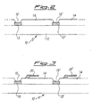
- Figs. 6 and 7 show, partially in section, a support of the invention.
- a support 60 comprises a base 61 of the same kind and dimensions of base 11 previously described, but in which are obtained hollows 65, 65', ..., localized in areas 62, 62', ..., and fitted to contain gas absorbing material deposits 63, 63', .... Thanks to its peculiar hollows conformation, base 61, can substitute the assembly made up of base 11 and layer 14.
- Fig. 8 represents a solid state device 80, in particular a micromachine, which can be obtained from support 60 of Figs. 6 and 7 , through a process similar to the one described with reference to Figs. 3-5 and utilizing a covering element 70 provided with holes 71, ..., in correspondence with areas wherein, on support 60, structures 72, ..., are disposed and gas absorbing material deposits 63, 63', ..., are exposed.
- support 60 of the invention is utilized as covering element of a solid state device instead of as base of the same.
- the base on which micromachine is constructed is a traditional one, without gas absorbing material deposits.
Abstract
Description
- The present invention relates to a support for manufacturing microelectronic, microoptoelectronic or micromechanical devices with integrated deposit of gas absorbing material.
- Microelectronic devices (also called integrated electronic circuits, indicated in the field with the abbreviation ICs) are the base of the whole integrated electronic industry. Microoptoelectronic devices comprise, for example, new generation infrared radiation (IR) sensors which, unlike traditional ones, do not require cryogenic temperatures for their operation. These IR sensors are formed of an array of semiconductor material deposits, for example silicon, arranged in an evacuated chamber. Micromechanical devices (better known in the field as "micromachines" or its abbreviation MMs) are in developing step for applications such as miniaturized sensors or actuators: typical examples of micromachines are microaccelerometers, used as sensors to activate automobile airbags; micromotors, having gears and sprocket wheels of the size of a few microns, or optic switches, wherein a mirror surface with a size of the order of a few tens microns (µm) can be moved between two different positions, directing a light beam toward two different directions, one corresponding to the "on" condition and the other to the "off' condition of an optical circuit. In the following, all these devices will also be referred to with the general definition of solid state devices.
- ICs are manufactured by a technology comprising operations of deposit on a planar support of layers of material with different electric (or magnetic) functionality, alternated to selective removals thereof. The same techniques of depositions and selective removals are applied to microoptoelectronic or micromechanical devices construction as well. These are generally contained in housings formed, in their turn, with the same techniques. The support most commonly used in these productions is a silicon "slice" (said "wafer" in the field), about 1 mm thick and with a diameter up to 30 cm. On each of these wafers a very high number of devices is constructed; then, at the end of the manufacturing process, from these slices are separated, by mechanical or laser cut, the single devices in the case of micromachines, or parts including an array of some tens of devices in the IR sensors case.
- The deposition steps are carried out with such techniques as chemical deposition from vapor state, generally defined "CVD" from the English "Chemical Vapor Deposition", or physical deposition from vapor state or "PVD", from the English "Physical Vapor Deposition", the latter commonly indicated also with the English name "sputtering". Generally, selective removals are carried out through chemical or physical attacks with proper masking, as it is well known in the field.
- The integrated circuits and the micromachines are then encapsulated in polymeric, metallic or ceramic materials, essentially for mechanical protection reasons, before being inserted in the final destination apparatus (a computer, an automobile, etc.). On the contrary, IR radiation sensors are generally comprised in a chamber, facing one wall thereof defined as "window", transparent to the IR radiation.
- In some kinds of integrated circuits it is important to be able to control the gas diffusion in solid state devices: it is for example the case of ferroelectric memories, wherein hydrogen, diffusing through device layers, can reach the ferroelectric material (generally a ceramic oxide, such as lead titanate-zirconate, strontium-bismuth tantalate or titanate, or bismuth-lanthanum titanate), altering its correct behavior.
- Still more important is gas control and elimination in IR sensors and in micromachines. In the case of IR sensors, the gases possibly present in the chamber can either sorb part of the radiation or transport heat by convection from the window to the array of silicon deposits, modifying the measure. In micromachines, the mechanical friction between gas molecules and the moving part, due to the very small size of the latter, can lead to sensible deviations from the device's ideal operation; moreover, polar molecules such as water can cause phenomena of adhesion between the moving part and other parts, for example the support thereof, thus causing the device's failure. In the IR sensors with arrays of silicon deposits or in the micromachines, it is therefore fundamental to be capable of ensuring the housing to remain in vacuum for the whole device life.
- In order to minimize the gas amount in these devices, their production is usually conducted in vacuum chambers and resorting to pumping steps before the packaging thereof. Anyway the problem is not completely solved in this way, because the same materials which form the devices can release gases, or these can permeate from outside during the device life.
- To remove also the gases entering in solid state devices during their life, it has been proposed to use materials that can absorb them. These materials comprise those commonly referred to as "getters, generally metals such as zirconium, titanium, vanadium, niobium or tantalum, or alloys thereof with other transition metals, with rare-earth elements or aluminum, having a very strong chemical affinity towards gases such as hydrogen, oxygen, water, carbon oxides and in some cases nitrogen; and drier materials, specific for moisture sorption, among which mainly the oxides of alkali or alkaline-earth metals. The use of materials for absorbing gases, particularly hydrogen, in ICs, is described for instance in patent
US-A-5,760,433 and in published Japanese patent applicationsJP-11-040761 JP-2000-40799 US 5,921,461 ; finally, the use of gas absorbing materials in micromachines is described for example in the article "Vacuum packaging for microsensors by glass-silicon anodic bonding" by H. Henmi et al., published on technical journal Sensors and Actuators A, vol. 43 (1994), at pages 243-248. - Localized deposits of gas absorbing materials can be obtained by CVD or sputtering during solid state devices productive steps. However, this procedure is not very appreciated by manufacturers of these devices, since the deposition of the absorbing material during devices production implies the need that the total process is added with a step of localized deposition of this material, generally carried out through the operations of resin deposition, resin local sensitization through radiations (generally UV), selective removal of the photosensitized resin, gas absorbing material deposition and subsequent removal of the resin and of the gas absorbing material thereon deposed, leaving the gas absorption material deposit in the area from which the photosensitized resin had been removed. Moreover, the deposit of the gas absorbing material in the production line has the disadvantage that increasing the number of different steps of the process and of the materials therein used, also the risk of "cross-pollution" among the different chambers in which said different steps are carried out increases, with following possible increase of waste products because of contamination.
- The object of the present invention is to overcome the above-described problems of the prior art and, particularly, to simplify the manufacturing of solid state devices.
- This object is achieved according to the present invention with a support for manufacturing microelectronic, microoptoelectronic or micromechanical devices, the main characteristics of which are specified in
claim 1 and other characteristics of which are specified in the following claims. - The support of the invention is practically similar to silicon wafers commonly used in industry having, however, a gas absorption material (in'the form of discrete deposits) deposited in hollings onto the surface on which the microelectronic or micromechanical devices are constructed.
- The invention will be described below with reference to the drawings in which:
-
Fig. 1 shows in perspective, partially in section, a support; -
Fig. 2 shows a sectional view of the support inFig. 1 ; -
Figs 3-5 represent operative phases for constructing a solid state device starting from the support ofFig. 1 ; -
Fig. 6 shows in perspective, partially in section, a support according to the invention; -
Fig. 7 shows a sectional view of support inFig. 6 ; -
Fig. 8 represent a solid state device obtainable from support ofFig. 6 ; and -
Fig. 9 shows a sectional view of a solid state device constructed starting from the support ofFig. 6 . - For the sake of description clarity, in the drawings height-diameter ratio of supports of the invention and lateral dimensions of gas absorbing material deposits upon the base are exaggerated with respect to real dimensions. Moreover, in the drawings, supports are always represented with a wafer geometry, that is a low disk of material, because this is the geometry commonly adopted by the producers of solid state devices, but this geometry could be also different, for example square or rectangular.
- In
figure 1 is shown a partial sectional view of asupport 10. Said support, 10, comprises a base, 11, having the only function of backing the support and devices deriving therefrom, and constitutes nearly the whole thickness of support 10 (within the range of millimeters). Base material can be a metal, a ceramic, a glass or a semiconductor, preferably silicon. - In
areas 12, 12', ..., of the surface ofbase 11,discrete deposits 13, 13', ... of a gas absorbing material are obtained. Then these deposits are covered with alayer 14 of a material compatible with ICs or MMs production process. Thislayer 14 performs duty of anchorage for layers subsequently deposed thereon to construct ICs, microoptoelectronic devices or MMs, or it can be even itself the layer in which these devices are constructed (for example micromachines moving parts can be obtained in this layer by removing parts thereof). Moreover the final device's soldering can be possibly made directly on the edge oflayer 14. - As also shown in
Fig. 2 , inlayer 14, in correspondence ofdeposits 13, 13',..., are then realizedpassages 15, 15', ..., having function of exposing the gas absorbing material to theatmosphere surrounding support 10.Passages 15, 15', ..., can be made by selective removal oflayer 14 upondeposits 13, 13', ..., through removing techniques know in the art. - The gas absorbing material utilized for
deposits 13, 13', ... can be any material free from the phenomenon of lost particles, chosen among materials commonly called getter, capable of absorbing various gas molecules, and drier materials, specific for the absorption of water vapor. - In case of a getter material, it can be a metal such as Zr, Ti, Nb, Ta, V; an alloy among these metals or among these and one or more elements, chosen among Cr, Mn, Fe, Co, Ni, Al, Y, La and rare-earths, like binary alloys Ti-V, Zr-V, Zr-Fe and Zr-Ni, ternary alloys Zr-Mn-Fe or Zr-V-Fe, or alloys with more components. For this application, preferred getter materials are titanium, zirconium, the alloy of weight percentage composition Zr 84%-Al 16%, produced and sold from applicant with name St 101®, the alloy of weight
percentage composition Zr 70%-V 24.6%-Fe 5.4%, produced and sold from applicant with name St 707® and the alloy of weight percentage composition Zr 80.8%-Co 14.2%-TR 5% (wherein TR is a rare-earth, yttrium, lanthanum or mixtures thereof), produced and sold from applicant with name St 787; in case the getter material is not completely free from the lost particles phenomenon, it can be properly treated so to reduce or eliminate said phenomenon, for example through a partial sintering or annealing treatment. - In case of drier materials, these are preferably chosen among the oxides of alkali or alkaline-earth metals; particularly preferred is the use of calcium oxide, CaO, that does not pose safety or environmental problems during production, use or disposal of devices containing it. An oxide layer may be obtained for instance through the so-called "reactive sputtering" technique, depositing the alkali or alkaline-earth metal of interest under an atmosphere of a rare gas (generally argon) in which a low percentage of oxygen is present, so that the metal is converted to its oxide during deposition. These layers are generally compact and free from the problem of lost particles.
-
Deposits 13, 13', ..., can be obtained through known techniques of selective deposition, and have thickness in the range between about 0,1 and 5 µm: with thickness values lower than the indicated ones, gas sorption capability is excessively reduced, while with higher thickness values deposition times are extended without any real advantages on sorption properties. Said deposits have lateral dimensions variable within wide ranges depending on final destination device: for example, if utilization is expected in ICs, lateral dimension will be within the range of some micron or less, while in the case of MMs, dimensions can be included between a few tens and a few hundreds micron. -
Material constituting layer 14 is one of the materials normally used as substate in solid state devices production; it can be a so-called III-V material (for example, GaAs o InP), or preferably silicon.Layer 14 can be obtained by sputtering, epitaxy, CVD or by others techniques known in the field. It has a variable thickness, which is generally lower than 60 µm in areas free fromdeposits 13, 13', ..., and preferably within the range of about 1-20 µm. - To help adhesion,
layer 14 is preferably realized with the same material asbase 11; preferred combination is silicon (mono- or polycrystalline) forbase 11, and silicon grown by epitaxy forlayer 14. - Upper surface of
layer 14 can also be treated thus modifying its chemical composition, for example forming an oxide or a nitride, in view of the following operations of devices production. - Supports can be therefore utilized in the production of solid state devices of every kind. As appears from previous description, in supports completed and ready for utilization or commercialization, deposits of gas absorbing material are "uncovered", that is, exposed to external atmosphere. To avoid the risk of excessive passivation and damaging of the absorbing material, it is then preferable to keep supports inside boxes under inert atmosphere, for instance argon or dry nitrogen, as known in the art.
-
Figs. 3-5 show a possible use ofsupport 10 in solid state devices production, particularly referring to micromachines production. However, the same support could be utilized for manufacturing other solid state devices. - Upon areas of surface of
layer 14 withoutpassages 15, 15', ..., are manufactured structures comprising micromachine mobile parts, schematized aselements 30, 30', ... inFig. 3 . Whenstructures 30, 30', ...production (including contacts for outside electric connection of every single micromachine, not shown in the drawing) is finished, a coveringelement 40 is placed oversupport 10, as shown in section inFig. 4 . Said covering element is generally realized with thesame base 11 materials and it has to be easily fixable to layer 14 (silicon utilization is preferred). Coveringelement 40 can have holes, 41, 41', ..., in correspondence with areas wherein, onsupport 10,structures 30, 30', ..., arc obtained anddeposits 13, 13', ..., of gas absorbing material are exposed. In particular each of said holes will be so wide that, whensupport 10 and coveringelement 40 are fixed together, aspace 42, 42', ..., is obtained wherein a structure like 30, 30', ..., and apassage 15, 15', ..., giving access to the gas absorbing material, are contained, so that this latter is in direct contact withspace 42, 42', ..., and is able to sorb gas possibly present or released during time in said space. Finally, single micromachines, as the one represented inFig. 5 , are obtained by cutting the whole made up ofsupport 10 and coveringelement 40 along their adhesion areas. -
Figs. 6 and7 show, partially in section, a support of the invention. Also in this case asupport 60 comprises abase 61 of the same kind and dimensions ofbase 11 previously described, but in which are obtainedhollows 65, 65', ..., localized inareas 62, 62', ..., and fitted to contain gas absorbingmaterial deposits 63, 63', .... Thanks to its peculiar hollows conformation,base 61, can substitute the assembly made up ofbase 11 andlayer 14. -
Fig. 8 represents asolid state device 80, in particular a micromachine, which can be obtained fromsupport 60 ofFigs. 6 and7 , through a process similar to the one described with reference toFigs. 3-5 and utilizing a coveringelement 70 provided withholes 71, ..., in correspondence with areas wherein, onsupport 60,structures 72, ..., are disposed and gas absorbingmaterial deposits 63, 63', ..., are exposed. - In a variation of the processes defined above, the result of which is
micromachine 90 shown infigure 9 ,support 60 of the invention is utilized as covering element of a solid state device instead of as base of the same. In this case, the base on which micromachine is constructed is a traditional one, without gas absorbing material deposits. Hollow 65, obtained insidebase 61, forms thus a space for housingmobile structure 91 and, at the same time, the passage giving access to gas absorbing material.
Claims (15)
- A support (60) for manufacturing micromechanical devices, comprising a base (61) having functions of mechanic support, characterized in that said base is provided with hollows (65, 65', ...) containing discrete deposits (63, 63', ...) of a gas absorbing material which are at least partially exposed to the atmosphere present nearby said support (60), said hollows (65, 65', ...) forming a space for housing mobile structures (91) of said micromechanical devices.
- A support according to claim 1 characterized in that material with which said base (61) is realized is chosen among a metal, a ceramic, a glass or a semiconductor.
- A support according to claim 2, characterized in that said material is silicon.
- A support according to claim 1 characterized in that said gas absorbing material is a getter material.
- A support according to claim 4 wherein said getter material is chosen among the metals Zr, Ti, Nb, Ta, V, alloys among these metals or alloys among these metals and one or more elements chosen among Cr, Mn, Fe, Co, Ni, Al, Y, La and rare-earths.
- A support according to claim 5 characterized in that said getter material is titanium.
- A support according to claim 5 characterized in that said getter material is zirconium.
- A support according to claim 5 characterized in that said getter material is an alloy having a weight percentage composition Zr 84%-A1 16%.
- A support according to claim 5 characterized in that said getter material is an alloy having a weight percentage composition Zr 70%-V 24.6%-Fe 5.4%.
- A support according to claim 5 characterized in that said getter material is an alloy having a weight percentage composition Zr 80.8%-Co 14.2%-TR 5%, wherein TR means a rare earth, yttrium, lanthanum or their mixtures.
- A support according to claim 1, characterized in that said gas absorbing material is a drier material.
- A support according to claim 11 characterized in that said drier material is chosen among the oxides of alkali or alkaline-earth metals.
- A support according to claim 12 characterized in that said drier material is calcium oxide.
- A support according to claim 1, characterized in that said discrete deposits (63, 63', ...) of gas absorbing material have a thickness within the range 0,1-5 µm.
- Use of a support of claim 1 as covering element in the production of a micromechanical device.
Applications Claiming Priority (5)
| Application Number | Priority Date | Filing Date | Title |
|---|---|---|---|
| IT2001MI001558A ITMI20011558A1 (en) | 2001-07-20 | 2001-07-20 | SUPPORT FOR MICRO-ELECTRONIC OR MICRO-ELECTRONIC OR MICROMECHANICAL DEVICES |
| ITMI20011558 | 2001-07-20 | ||
| IT2002MI000688A ITMI20020688A1 (en) | 2002-04-03 | 2002-04-03 | SUPPORT FOR MICRO-ELECTRONIC OR MICRO-ELECTRONIC OR MICROMECHANICAL DEVICES |
| ITMI20020068 | 2002-04-03 | ||
| PCT/IT2002/000466 WO2003009318A2 (en) | 2001-07-20 | 2002-07-16 | Support with getter-material for microelectronic, microoptoelectronic or micromechanical device |
Publications (2)
| Publication Number | Publication Date |
|---|---|
| EP1412550A2 EP1412550A2 (en) | 2004-04-28 |
| EP1412550B1 true EP1412550B1 (en) | 2009-03-25 |
Family
ID=26332783
Family Applications (1)
| Application Number | Title | Priority Date | Filing Date |
|---|---|---|---|
| EP02755628A Expired - Lifetime EP1412550B1 (en) | 2001-07-20 | 2002-07-16 | Support with getter-material for micromechanical device |
Country Status (15)
| Country | Link |
|---|---|
| US (5) | US6897551B2 (en) |
| EP (1) | EP1412550B1 (en) |
| JP (5) | JP4068555B2 (en) |
| KR (1) | KR100611134B1 (en) |
| CN (1) | CN100503879C (en) |
| AT (1) | ATE426688T1 (en) |
| AU (1) | AU2002321832A1 (en) |
| CA (1) | CA2450412C (en) |
| DE (1) | DE60231715D1 (en) |
| DK (1) | DK1412550T3 (en) |
| ES (1) | ES2321913T3 (en) |
| HK (1) | HK1073336A1 (en) |
| MY (1) | MY135763A (en) |
| TW (1) | TW533188B (en) |
| WO (1) | WO2003009318A2 (en) |
Cited By (4)
| Publication number | Priority date | Publication date | Assignee | Title |
|---|---|---|---|---|
| EP2736071A1 (en) | 2012-11-22 | 2014-05-28 | Tronics Microsystems S.A. | Wafer level package with getter |
| EP2813464A1 (en) | 2013-06-12 | 2014-12-17 | Tronics Microsystems S.A. | Device with getter material |
| EP2813465A1 (en) | 2013-06-12 | 2014-12-17 | Tronics Microsystems S.A. | MEMS device with getter layer |
| US8981544B2 (en) | 2010-11-09 | 2015-03-17 | Commissariat A L'energie Atomique Et Aux Energies Alternatives | Packaging structure of a micro-device including a getter material |
Families Citing this family (39)
| Publication number | Priority date | Publication date | Assignee | Title |
|---|---|---|---|---|
| TW583049B (en) * | 2001-07-20 | 2004-04-11 | Getters Spa | Support with integrated deposit of gas absorbing material for manufacturing microelectronic, microoptoelectronic or micromechanical devices |
| TW533188B (en) * | 2001-07-20 | 2003-05-21 | Getters Spa | Support for microelectronic, microoptoelectronic or micromechanical devices |
| WO2005015637A1 (en) * | 2003-08-08 | 2005-02-17 | Matsushita Electric Industrial Co., Ltd. | Electronic device and method of producing the same |
| US7871660B2 (en) * | 2003-11-14 | 2011-01-18 | Saes Getters, S.P.A. | Preparation of getter surfaces using caustic chemicals |
| ITMI20032208A1 (en) * | 2003-11-14 | 2005-05-15 | Getters Spa | CATODO WITH INTEGRATED AND LOW FUNCTION GETTER WORK FOR COLD CATO LAMPS. |
| ITMI20032209A1 (en) * | 2003-11-14 | 2005-05-15 | Getters Spa | PROCESS FOR THE PRODUCTION OF DEVICES THAT REQUIRE A NON-EVAPORABLE GETTER MATERIAL FOR THEIR OPERATION. |
| US8124434B2 (en) | 2004-09-27 | 2012-02-28 | Qualcomm Mems Technologies, Inc. | Method and system for packaging a display |
| US20060076634A1 (en) * | 2004-09-27 | 2006-04-13 | Lauren Palmateer | Method and system for packaging MEMS devices with incorporated getter |
| ITMI20052343A1 (en) * | 2005-12-06 | 2007-06-07 | Getters Spa | PROCESS FOR THE PRODUCTION OF MICROMECHANICAL DEVICES CONTAINING A GETTER MATERIAL AND DEVICES SO MANUFACTURED |
| JP2008135690A (en) * | 2006-10-30 | 2008-06-12 | Denso Corp | Semiconductor physical quantity sensor and method of manufacturing same |
| US7923790B1 (en) * | 2007-03-09 | 2011-04-12 | Silicon Laboratories Inc. | Planar microshells for vacuum encapsulated devices and damascene method of manufacture |
| US7736929B1 (en) | 2007-03-09 | 2010-06-15 | Silicon Clocks, Inc. | Thin film microshells incorporating a getter layer |
| US7595209B1 (en) | 2007-03-09 | 2009-09-29 | Silicon Clocks, Inc. | Low stress thin film microshells |
| US7659150B1 (en) | 2007-03-09 | 2010-02-09 | Silicon Clocks, Inc. | Microshells for multi-level vacuum cavities |
| EP2031677B1 (en) * | 2007-08-31 | 2011-10-12 | Technical University of Denmark | Removal of impurity phases from electrochemical devices |
| US8349635B1 (en) | 2008-05-20 | 2013-01-08 | Silicon Laboratories Inc. | Encapsulated MEMS device and method to form the same |
| FR2933389B1 (en) * | 2008-07-01 | 2010-10-29 | Commissariat Energie Atomique | STRUCTURE BASED ON SUSPENDED GETTER MATERIAL |
| JP2010019933A (en) * | 2008-07-08 | 2010-01-28 | Seiko Epson Corp | Actuator, optical scanner and image forming apparatus |
| ITMI20090410A1 (en) | 2009-03-18 | 2010-09-19 | Getters Spa | NON EVAPORABLE GETTER ALLOYS PARTICULARLY SUITABLE FOR HYDROGEN ABSORPTION |
| FR2950877B1 (en) | 2009-10-07 | 2012-01-13 | Commissariat Energie Atomique | CAVITY STRUCTURE COMPRISING A BONDING INTERFACE BASED ON MATERIAL GETTER |
| FR2950876B1 (en) | 2009-10-07 | 2012-02-10 | Commissariat Energie Atomique | METHOD FOR TREATING A GETTER MATERIAL AND METHOD FOR ENCAPSULATING SUCH A GETTER MATERIAL |
| JP5298047B2 (en) | 2010-02-26 | 2013-09-25 | 日立オートモティブシステムズ株式会社 | Manufacturing method of composite sensor |
| FR2967150A1 (en) | 2010-11-09 | 2012-05-11 | Commissariat Energie Atomique | PROCESS FOR PRODUCING A SUBSTRATE WITH BURNED LAYERS OF GETTER MATERIAL |
| US8395229B2 (en) | 2011-03-11 | 2013-03-12 | Institut National D'optique | MEMS-based getter microdevice |
| JP5541306B2 (en) | 2011-05-27 | 2014-07-09 | 株式会社デンソー | Mechanical quantity sensor device and manufacturing method thereof |
| US9491802B2 (en) | 2012-02-17 | 2016-11-08 | Honeywell International Inc. | On-chip alkali dispenser |
| DE102012207165A1 (en) | 2012-04-30 | 2013-10-31 | Robert Bosch Gmbh | Micro-electromechanical device e.g. micro-electromechanical sensor such as inertial sensor, has electrically conductive metallization portion which is arranged on surface of substrate and is partially formed of chemically active getter |
| US9018715B2 (en) | 2012-11-30 | 2015-04-28 | Silicon Laboratories Inc. | Gas-diffusion barriers for MEMS encapsulation |
| US10160638B2 (en) * | 2013-01-04 | 2018-12-25 | Taiwan Semiconductor Manufacturing Company, Ltd. | Method and apparatus for a semiconductor structure |
| US9029773B2 (en) * | 2013-02-24 | 2015-05-12 | Vlad Novotny | Sealed infrared imagers |
| WO2014129666A1 (en) * | 2013-02-25 | 2014-08-28 | 京セラ株式会社 | Package for housing electronic component and electronic device |
| EP3544353B1 (en) | 2014-03-20 | 2021-12-08 | Kyocera Corporation | User equipment, base station and corresponding methods |
| US9422149B2 (en) | 2014-07-25 | 2016-08-23 | Semiconductor Manufacturing International (Shanghai) Corporation | Trapped sacrificial structures and methods of manufacturing same using thin-film encapsulation |
| US11078075B2 (en) | 2015-12-31 | 2021-08-03 | Taiwan Semiconductor Manufacturing Company Ltd. | Packaging method and associated packaging structure |
| KR102145769B1 (en) * | 2016-01-25 | 2020-08-19 | 교세라 가부시키가이샤 | Measurement sensor package and measurement sensor |
| DE102017210459A1 (en) | 2017-06-22 | 2018-12-27 | Robert Bosch Gmbh | Micromechanical device with a first cavity and a second cavity |
| FR3072788B1 (en) | 2017-10-24 | 2020-05-29 | Commissariat A L'energie Atomique Et Aux Energies Alternatives | MODULAR INFRARED RADIATION SOURCE |
| FR3088319B1 (en) | 2018-11-08 | 2020-10-30 | Ulis | HERMETIC CASE INCLUDING A GETTER, OPTOELECTRONIC COMPONENT OR MEMS DEVICE INTEGRATING SUCH A HERMETIC CASE AND ASSOCIATED MANUFACTURING PROCESS |
| WO2023186704A1 (en) * | 2022-04-01 | 2023-10-05 | Saes Getters S.P.A. | Substrate comprising a base and an integrated getter film for manufacturing microelectronic devices |
Family Cites Families (56)
| Publication number | Priority date | Publication date | Assignee | Title |
|---|---|---|---|---|
| US503261A (en) * | 1893-08-15 | bereuter | ||
| US3214381A (en) * | 1962-12-05 | 1965-10-26 | Bell Telephone Labor Inc | Barium oxide moisture getter preparation |
| JPS56137658A (en) * | 1980-03-31 | 1981-10-27 | Chiyou Lsi Gijutsu Kenkyu Kumiai | Semiconductor device |
| US4426769A (en) * | 1981-08-14 | 1984-01-24 | Amp Incorporated | Moisture getter for integrated circuit packages |
| US5032461A (en) | 1983-12-19 | 1991-07-16 | Spectrum Control, Inc. | Method of making a multi-layered article |
| JPS63198320A (en) * | 1987-02-13 | 1988-08-17 | Mitsubishi Electric Corp | Crystal growth method |
| US5083466A (en) | 1988-07-14 | 1992-01-28 | University Of Hawaii | Multidimensional force sensor |
| US5192240A (en) | 1990-02-22 | 1993-03-09 | Seiko Epson Corporation | Method of manufacturing a microelectronic vacuum device |
| GB9015820D0 (en) | 1990-07-18 | 1990-09-05 | Raychem Ltd | Processing microchips |
| US5108026A (en) | 1991-05-14 | 1992-04-28 | Motorola Inc. | Eutectic bonding of metal to ceramic |
| JP2814445B2 (en) | 1992-09-16 | 1998-10-22 | インターナショナル・ビジネス・マシーンズ・コーポレイション | Selective low-temperature chemical vapor deposition of gold. |
| KR0139489B1 (en) * | 1993-07-08 | 1998-06-01 | 호소야 레이지 | Electric field radiate type display equipment |
| CA2179052C (en) | 1993-12-13 | 2001-02-13 | Robert E. Higashi | Integrated silicon vacuum micropackage for infrared devices |
| JP3456257B2 (en) * | 1994-05-27 | 2003-10-14 | 株式会社デンソー | Electronic device package |
| US5453659A (en) * | 1994-06-10 | 1995-09-26 | Texas Instruments Incorporated | Anode plate for flat panel display having integrated getter |
| JPH0878569A (en) * | 1994-09-07 | 1996-03-22 | Nippondenso Co Ltd | Package for electronic part |
| US5599749A (en) | 1994-10-21 | 1997-02-04 | Yamaha Corporation | Manufacture of micro electron emitter |
| CA2162095A1 (en) | 1994-12-27 | 1996-06-28 | Jeffery Alan Demeritt | Getter housing for electronic packages |
| US5668018A (en) * | 1995-06-07 | 1997-09-16 | International Business Machines Corporation | Method for defining a region on a wall of a semiconductor structure |
| US5614785A (en) | 1995-09-28 | 1997-03-25 | Texas Instruments Incorporated | Anode plate for flat panel display having silicon getter |
| JPH09127151A (en) * | 1995-11-01 | 1997-05-16 | Murata Mfg Co Ltd | Acceleration sensor |
| US5837935A (en) | 1996-02-26 | 1998-11-17 | Ford Motor Company | Hermetic seal for an electronic component having a secondary chamber |
| JPH09306920A (en) | 1996-05-20 | 1997-11-28 | Hitachi Ltd | Semiconductor integrated circuit device and its manufacture |
| US5760433A (en) * | 1996-05-31 | 1998-06-02 | Hughes Electronics | In situ reactive layers for protection of ferroelectric integrated circuits |
| JPH09318656A (en) * | 1996-05-31 | 1997-12-12 | Hitachi Ltd | Electrostatic capacity type acceleration sensor |
| IT1283484B1 (en) * | 1996-07-23 | 1998-04-21 | Getters Spa | METHOD FOR THE PRODUCTION OF THIN SUPPORTED LAYERS OF NON-EVAPORABLE GETTER MATERIAL AND GETTER DEVICES THUS PRODUCED |
| US6673400B1 (en) * | 1996-10-15 | 2004-01-06 | Texas Instruments Incorporated | Hydrogen gettering system |
| JPH10176768A (en) | 1996-11-27 | 1998-06-30 | Xerox Corp | Microdevice supporting system and array of microdevice |
| US5837934A (en) | 1996-12-02 | 1998-11-17 | Midway Games Inc. | Shock insulated container for hard disk drives |
| JPH10188460A (en) | 1996-12-25 | 1998-07-21 | Sony Corp | Optical disk device and optical disk recording medium |
| IT1290451B1 (en) | 1997-04-03 | 1998-12-03 | Getters Spa | NON-EVAPORABLE GETTER ALLOYS |
| US5921461A (en) * | 1997-06-11 | 1999-07-13 | Raytheon Company | Vacuum package having vacuum-deposited local getter and its preparation |
| US5951750A (en) * | 1997-06-19 | 1999-09-14 | Engelhard Corporation | Anti-yellowing polyolefin compositions containing pearlescent pigment to prevent yellowing and method therefore |
| JPH1140761A (en) | 1997-07-23 | 1999-02-12 | Fujitsu Ltd | Semiconductor device and manufacture thereof |
| US5961362A (en) * | 1997-09-09 | 1999-10-05 | Motorola, Inc. | Method for in situ cleaning of electron emitters in a field emission device |
| US5866978A (en) * | 1997-09-30 | 1999-02-02 | Fed Corporation | Matrix getter for residual gas in vacuum sealed panels |
| US6359333B1 (en) * | 1998-03-31 | 2002-03-19 | Honeywell International Inc. | Wafer-pair having deposited layer sealed chambers |
| US6499354B1 (en) * | 1998-05-04 | 2002-12-31 | Integrated Sensing Systems (Issys), Inc. | Methods for prevention, reduction, and elimination of outgassing and trapped gases in micromachined devices |
| US6843936B1 (en) | 1998-10-22 | 2005-01-18 | Texas Instruments Incorporated | Getter for enhanced micromechanical device performance |
| JP3677409B2 (en) * | 1999-03-05 | 2005-08-03 | 京セラ株式会社 | Surface acoustic wave device and manufacturing method thereof |
| JP2000277525A (en) * | 1999-03-26 | 2000-10-06 | Toshiba Ceramics Co Ltd | Silicon wafer for semiconductor and its manufacture |
| IT1312248B1 (en) * | 1999-04-12 | 2002-04-09 | Getters Spa | METHOD TO INCREASE THE PRODUCTIVITY OF THIN DISTRICT DISPOSAL PROCESSES ON A SUBSTRATE AND GETTER DEVICES FOR |
| US6449354B1 (en) * | 1999-06-08 | 2002-09-10 | Nortel Networks Limited | Communication system, article and method of configuring and establishing a connection therein |
| US6265246B1 (en) * | 1999-07-23 | 2001-07-24 | Agilent Technologies, Inc. | Microcap wafer-level package |
| US6228675B1 (en) * | 1999-07-23 | 2001-05-08 | Agilent Technologies, Inc. | Microcap wafer-level package with vias |
| US6400009B1 (en) * | 1999-10-15 | 2002-06-04 | Lucent Technologies Inc. | Hermatic firewall for MEMS packaging in flip-chip bonded geometry |
| GB9927806D0 (en) | 1999-11-24 | 2000-01-26 | Isis Innovation | Genetic indicators of tobacco consumption |
| US6477901B1 (en) | 1999-12-21 | 2002-11-12 | Integrated Sensing Systems, Inc. | Micromachined fluidic apparatus |
| JP2001196486A (en) * | 2000-01-07 | 2001-07-19 | Murata Mfg Co Ltd | Reduced-pressure package structure and manufacturing method thereof |
| US6410847B1 (en) * | 2000-07-25 | 2002-06-25 | Trw Inc. | Packaged electronic system having selectively plated microwave absorbing cover |
| CN1127138C (en) * | 2000-09-15 | 2003-11-05 | 北京大学 | Low-temp MEMS vacuum sealing technique for metals |
| US6534850B2 (en) | 2001-04-16 | 2003-03-18 | Hewlett-Packard Company | Electronic device sealed under vacuum containing a getter and method of operation |
| TW583049B (en) * | 2001-07-20 | 2004-04-11 | Getters Spa | Support with integrated deposit of gas absorbing material for manufacturing microelectronic, microoptoelectronic or micromechanical devices |
| TW533188B (en) * | 2001-07-20 | 2003-05-21 | Getters Spa | Support for microelectronic, microoptoelectronic or micromechanical devices |
| EP1310380A1 (en) | 2001-11-07 | 2003-05-14 | SensoNor asa | A micro-mechanical device and method for producing the same |
| US6923625B2 (en) | 2002-01-07 | 2005-08-02 | Integrated Sensing Systems, Inc. | Method of forming a reactive material and article formed thereby |
-
2002
- 2002-07-12 TW TW091115738A patent/TW533188B/en not_active IP Right Cessation
- 2002-07-16 WO PCT/IT2002/000466 patent/WO2003009318A2/en active Application Filing
- 2002-07-16 ES ES02755628T patent/ES2321913T3/en not_active Expired - Lifetime
- 2002-07-16 CA CA002450412A patent/CA2450412C/en not_active Expired - Lifetime
- 2002-07-16 EP EP02755628A patent/EP1412550B1/en not_active Expired - Lifetime
- 2002-07-16 KR KR1020047000915A patent/KR100611134B1/en active IP Right Grant
- 2002-07-16 JP JP2003514572A patent/JP4068555B2/en not_active Expired - Lifetime
- 2002-07-16 DK DK02755628T patent/DK1412550T3/en active
- 2002-07-16 AT AT02755628T patent/ATE426688T1/en active
- 2002-07-16 CN CNB028147103A patent/CN100503879C/en not_active Expired - Lifetime
- 2002-07-16 DE DE60231715T patent/DE60231715D1/en not_active Expired - Lifetime
- 2002-07-16 AU AU2002321832A patent/AU2002321832A1/en not_active Abandoned
- 2002-07-18 MY MYPI20022726A patent/MY135763A/en unknown
- 2002-07-19 US US10/201,657 patent/US6897551B2/en not_active Ceased
-
2005
- 2005-02-25 US US11/067,526 patent/US7534658B2/en not_active Expired - Lifetime
- 2005-03-01 US US11/070,728 patent/US7808091B2/en not_active Expired - Fee Related
- 2005-07-11 HK HK05105829.1A patent/HK1073336A1/en not_active IP Right Cessation
-
2007
- 2007-10-31 US US11/982,279 patent/US7566957B2/en not_active Expired - Lifetime
- 2007-11-14 JP JP2007295918A patent/JP2008118147A/en not_active Withdrawn
-
2008
- 2008-04-24 US US12/150,287 patent/USRE44255E1/en not_active Expired - Lifetime
-
2011
- 2011-10-19 JP JP2011229923A patent/JP2012051106A/en not_active Withdrawn
-
2013
- 2013-12-13 JP JP2013257638A patent/JP2014058040A/en active Pending
-
2015
- 2015-12-09 JP JP2015240035A patent/JP6140259B2/en not_active Expired - Lifetime
Cited By (4)
| Publication number | Priority date | Publication date | Assignee | Title |
|---|---|---|---|---|
| US8981544B2 (en) | 2010-11-09 | 2015-03-17 | Commissariat A L'energie Atomique Et Aux Energies Alternatives | Packaging structure of a micro-device including a getter material |
| EP2736071A1 (en) | 2012-11-22 | 2014-05-28 | Tronics Microsystems S.A. | Wafer level package with getter |
| EP2813464A1 (en) | 2013-06-12 | 2014-12-17 | Tronics Microsystems S.A. | Device with getter material |
| EP2813465A1 (en) | 2013-06-12 | 2014-12-17 | Tronics Microsystems S.A. | MEMS device with getter layer |
Also Published As
Similar Documents
| Publication | Publication Date | Title |
|---|---|---|
| EP1412550B1 (en) | Support with getter-material for micromechanical device | |
| US8193623B2 (en) | Support with integrated deposit of gas absorbing material for manufacturing microelectronic, microoptoelectronic or micromechanical devices | |
| US6923625B2 (en) | Method of forming a reactive material and article formed thereby | |
| KR102401863B1 (en) | Method for manufacturing a device comprising a hermetically sealed vacuum housing and getter | |
| JP5133680B2 (en) | Packaging for a microelectromechanical system and method for manufacturing the same | |
| KR20180058221A (en) | Use of external getter to lower package pressure | |
| ITMI20011558A1 (en) | SUPPORT FOR MICRO-ELECTRONIC OR MICRO-ELECTRONIC OR MICROMECHANICAL DEVICES | |
| ITMI20011557A1 (en) | SUPPORT FOR THE PRODUCTION OF MICRO-ELECTRONIC OR MICRO-ELECTRONIC OR MICROMECHANICAL DEVICES WITH INTEGRATED STORAGE OF GETTER MATERIAL |
Legal Events
| Date | Code | Title | Description |
|---|---|---|---|
| PUAI | Public reference made under article 153(3) epc to a published international application that has entered the european phase |
Free format text: ORIGINAL CODE: 0009012 |
|
| 17P | Request for examination filed |
Effective date: 20031227 |
|
| AK | Designated contracting states |
Kind code of ref document: A2 Designated state(s): AT BE BG CH CY CZ DE DK EE ES FI FR GB GR IE IT LI LU MC NL PT SE SK TR |
|
| AX | Request for extension of the european patent |
Extension state: AL LT LV MK RO SI |
|
| 17Q | First examination report despatched |
Effective date: 20060725 |
|
| 17Q | First examination report despatched |
Effective date: 20060725 |
|
| GRAP | Despatch of communication of intention to grant a patent |
Free format text: ORIGINAL CODE: EPIDOSNIGR1 |
|
| RTI1 | Title (correction) |
Free format text: SUPPORT WITH GETTER-MATERIAL FOR MICROMECHANICAL DEVICE |
|
| GRAP | Despatch of communication of intention to grant a patent |
Free format text: ORIGINAL CODE: EPIDOSNIGR1 |
|
| GRAS | Grant fee paid |
Free format text: ORIGINAL CODE: EPIDOSNIGR3 |
|
| GRAA | (expected) grant |
Free format text: ORIGINAL CODE: 0009210 |
|
| AK | Designated contracting states |
Kind code of ref document: B1 Designated state(s): AT BE BG CH CY CZ DE DK EE ES FI FR GB GR IE IT LI LU MC NL PT SE SK TR |
|
| REG | Reference to a national code |
Ref country code: GB Ref legal event code: FG4D |
|
| REG | Reference to a national code |
Ref country code: CH Ref legal event code: EP |
|
| REG | Reference to a national code |
Ref country code: CH Ref legal event code: NV Representative=s name: RIEDERER HASLER & PARTNER PATENTANWAELTE AG |
|
| REG | Reference to a national code |
Ref country code: IE Ref legal event code: FG4D |
|
| REF | Corresponds to: |
Ref document number: 60231715 Country of ref document: DE Date of ref document: 20090507 Kind code of ref document: P |
|
| REG | Reference to a national code |
Ref country code: DK Ref legal event code: T3 Ref country code: SE Ref legal event code: TRGR |
|
| REG | Reference to a national code |
Ref country code: ES Ref legal event code: FG2A Ref document number: 2321913 Country of ref document: ES Kind code of ref document: T3 |
|
| PG25 | Lapsed in a contracting state [announced via postgrant information from national office to epo] |
Ref country code: PT Free format text: LAPSE BECAUSE OF FAILURE TO SUBMIT A TRANSLATION OF THE DESCRIPTION OR TO PAY THE FEE WITHIN THE PRESCRIBED TIME-LIMIT Effective date: 20090901 Ref country code: EE Free format text: LAPSE BECAUSE OF FAILURE TO SUBMIT A TRANSLATION OF THE DESCRIPTION OR TO PAY THE FEE WITHIN THE PRESCRIBED TIME-LIMIT Effective date: 20090325 |
|
| PG25 | Lapsed in a contracting state [announced via postgrant information from national office to epo] |
Ref country code: SK Free format text: LAPSE BECAUSE OF FAILURE TO SUBMIT A TRANSLATION OF THE DESCRIPTION OR TO PAY THE FEE WITHIN THE PRESCRIBED TIME-LIMIT Effective date: 20090325 |
|
| PG25 | Lapsed in a contracting state [announced via postgrant information from national office to epo] |
Ref country code: BG Free format text: LAPSE BECAUSE OF FAILURE TO SUBMIT A TRANSLATION OF THE DESCRIPTION OR TO PAY THE FEE WITHIN THE PRESCRIBED TIME-LIMIT Effective date: 20090625 |
|
| PLBE | No opposition filed within time limit |
Free format text: ORIGINAL CODE: 0009261 |
|
| STAA | Information on the status of an ep patent application or granted ep patent |
Free format text: STATUS: NO OPPOSITION FILED WITHIN TIME LIMIT |
|
| PG25 | Lapsed in a contracting state [announced via postgrant information from national office to epo] |
Ref country code: MC Free format text: LAPSE BECAUSE OF NON-PAYMENT OF DUE FEES Effective date: 20090731 |
|
| 26N | No opposition filed |
Effective date: 20091229 |
|
| PG25 | Lapsed in a contracting state [announced via postgrant information from national office to epo] |
Ref country code: GR Free format text: LAPSE BECAUSE OF FAILURE TO SUBMIT A TRANSLATION OF THE DESCRIPTION OR TO PAY THE FEE WITHIN THE PRESCRIBED TIME-LIMIT Effective date: 20090626 |
|
| PG25 | Lapsed in a contracting state [announced via postgrant information from national office to epo] |
Ref country code: LU Free format text: LAPSE BECAUSE OF NON-PAYMENT OF DUE FEES Effective date: 20090716 |
|
| PG25 | Lapsed in a contracting state [announced via postgrant information from national office to epo] |
Ref country code: CY Free format text: LAPSE BECAUSE OF FAILURE TO SUBMIT A TRANSLATION OF THE DESCRIPTION OR TO PAY THE FEE WITHIN THE PRESCRIBED TIME-LIMIT Effective date: 20090325 |
|
| REG | Reference to a national code |
Ref country code: FR Ref legal event code: PLFP Year of fee payment: 15 |
|
| REG | Reference to a national code |
Ref country code: FR Ref legal event code: PLFP Year of fee payment: 16 |
|
| REG | Reference to a national code |
Ref country code: FR Ref legal event code: PLFP Year of fee payment: 17 |
|
| PGFP | Annual fee paid to national office [announced via postgrant information from national office to epo] |
Ref country code: NL Payment date: 20210726 Year of fee payment: 20 |
|
| PGFP | Annual fee paid to national office [announced via postgrant information from national office to epo] |
Ref country code: FR Payment date: 20210726 Year of fee payment: 20 Ref country code: CZ Payment date: 20210702 Year of fee payment: 20 Ref country code: AT Payment date: 20210702 Year of fee payment: 20 Ref country code: FI Payment date: 20210728 Year of fee payment: 20 Ref country code: IT Payment date: 20210721 Year of fee payment: 20 Ref country code: IE Payment date: 20210727 Year of fee payment: 20 |
|
| PGFP | Annual fee paid to national office [announced via postgrant information from national office to epo] |
Ref country code: ES Payment date: 20210802 Year of fee payment: 20 Ref country code: DK Payment date: 20210728 Year of fee payment: 20 Ref country code: GB Payment date: 20210727 Year of fee payment: 20 Ref country code: SE Payment date: 20210728 Year of fee payment: 20 Ref country code: TR Payment date: 20210701 Year of fee payment: 20 Ref country code: CH Payment date: 20210804 Year of fee payment: 20 Ref country code: DE Payment date: 20210728 Year of fee payment: 20 Ref country code: BE Payment date: 20210727 Year of fee payment: 20 |
|
| REG | Reference to a national code |
Ref country code: DE Ref legal event code: R071 Ref document number: 60231715 Country of ref document: DE |
|
| REG | Reference to a national code |
Ref country code: DK Ref legal event code: EUP Expiry date: 20220716 |
|
| REG | Reference to a national code |
Ref country code: NL Ref legal event code: MK Effective date: 20220715 |
|
| REG | Reference to a national code |
Ref country code: CH Ref legal event code: PL |
|
| REG | Reference to a national code |
Ref country code: ES Ref legal event code: FD2A Effective date: 20220803 |
|
| REG | Reference to a national code |
Ref country code: FI Ref legal event code: MAE |
|
| REG | Reference to a national code |
Ref country code: GB Ref legal event code: PE20 Expiry date: 20220715 |
|
| REG | Reference to a national code |
Ref country code: BE Ref legal event code: MK Effective date: 20220716 |
|
| REG | Reference to a national code |
Ref country code: SE Ref legal event code: EUG |
|
| REG | Reference to a national code |
Ref country code: IE Ref legal event code: MK9A |
|
| REG | Reference to a national code |
Ref country code: AT Ref legal event code: MK07 Ref document number: 426688 Country of ref document: AT Kind code of ref document: T Effective date: 20220716 |
|
| PG25 | Lapsed in a contracting state [announced via postgrant information from national office to epo] |
Ref country code: IE Free format text: LAPSE BECAUSE OF EXPIRATION OF PROTECTION Effective date: 20220716 Ref country code: GB Free format text: LAPSE BECAUSE OF EXPIRATION OF PROTECTION Effective date: 20220715 Ref country code: ES Free format text: LAPSE BECAUSE OF EXPIRATION OF PROTECTION Effective date: 20220717 Ref country code: CZ Free format text: LAPSE BECAUSE OF EXPIRATION OF PROTECTION Effective date: 20220716 |