EP1416635B1 - Sensor device - Google Patents
Sensor device Download PDFInfo
- Publication number
- EP1416635B1 EP1416635B1 EP03024962A EP03024962A EP1416635B1 EP 1416635 B1 EP1416635 B1 EP 1416635B1 EP 03024962 A EP03024962 A EP 03024962A EP 03024962 A EP03024962 A EP 03024962A EP 1416635 B1 EP1416635 B1 EP 1416635B1
- Authority
- EP
- European Patent Office
- Prior art keywords
- electric wire
- coated electric
- coil
- detection circuit
- circuit board
- Prior art date
- Legal status (The legal status is an assumption and is not a legal conclusion. Google has not performed a legal analysis and makes no representation as to the accuracy of the status listed.)
- Expired - Lifetime
Links
- 238000001514 detection method Methods 0.000 claims description 102
- 229910000679 solder Inorganic materials 0.000 claims description 23
- 239000011248 coating agent Substances 0.000 claims description 9
- 238000000576 coating method Methods 0.000 claims description 9
- 230000010355 oscillation Effects 0.000 claims description 5
- 238000004804 winding Methods 0.000 description 31
- 239000010410 layer Substances 0.000 description 24
- 239000004020 conductor Substances 0.000 description 23
- 239000011347 resin Substances 0.000 description 23
- 229920005989 resin Polymers 0.000 description 23
- RYGMFSIKBFXOCR-UHFFFAOYSA-N Copper Chemical compound [Cu] RYGMFSIKBFXOCR-UHFFFAOYSA-N 0.000 description 19
- 238000000034 method Methods 0.000 description 16
- 239000011889 copper foil Substances 0.000 description 14
- 238000002347 injection Methods 0.000 description 14
- 239000007924 injection Substances 0.000 description 14
- 229910000859 α-Fe Inorganic materials 0.000 description 13
- 238000010586 diagram Methods 0.000 description 12
- 230000008021 deposition Effects 0.000 description 11
- 239000000463 material Substances 0.000 description 11
- 238000003466 welding Methods 0.000 description 8
- 239000002356 single layer Substances 0.000 description 7
- WABPQHHGFIMREM-UHFFFAOYSA-N lead(0) Chemical compound [Pb] WABPQHHGFIMREM-UHFFFAOYSA-N 0.000 description 5
- 229920006264 polyurethane film Polymers 0.000 description 5
- 239000000047 product Substances 0.000 description 5
- 230000000694 effects Effects 0.000 description 4
- 230000003287 optical effect Effects 0.000 description 4
- 239000004952 Polyamide Substances 0.000 description 3
- 238000003754 machining Methods 0.000 description 3
- 229920002647 polyamide Polymers 0.000 description 3
- 229920006267 polyester film Polymers 0.000 description 3
- 229920002635 polyurethane Polymers 0.000 description 3
- 239000004814 polyurethane Substances 0.000 description 3
- 238000007789 sealing Methods 0.000 description 3
- 230000035945 sensitivity Effects 0.000 description 3
- 230000000087 stabilizing effect Effects 0.000 description 3
- 239000004677 Nylon Substances 0.000 description 2
- 230000015556 catabolic process Effects 0.000 description 2
- 238000006731 degradation reaction Methods 0.000 description 2
- 230000004927 fusion Effects 0.000 description 2
- 230000001965 increasing effect Effects 0.000 description 2
- 230000001939 inductive effect Effects 0.000 description 2
- 239000013067 intermediate product Substances 0.000 description 2
- 230000001678 irradiating effect Effects 0.000 description 2
- 239000000696 magnetic material Substances 0.000 description 2
- 229920001778 nylon Polymers 0.000 description 2
- 229920006284 nylon film Polymers 0.000 description 2
- 229920000728 polyester Polymers 0.000 description 2
- 238000002360 preparation method Methods 0.000 description 2
- 230000001012 protector Effects 0.000 description 2
- 238000005476 soldering Methods 0.000 description 2
- 229910000976 Electrical steel Inorganic materials 0.000 description 1
- XUIMIQQOPSSXEZ-UHFFFAOYSA-N Silicon Chemical compound [Si] XUIMIQQOPSSXEZ-UHFFFAOYSA-N 0.000 description 1
- 238000004891 communication Methods 0.000 description 1
- 230000008602 contraction Effects 0.000 description 1
- 229910052802 copper Inorganic materials 0.000 description 1
- 239000010949 copper Substances 0.000 description 1
- 238000007765 extrusion coating Methods 0.000 description 1
- 238000011049 filling Methods 0.000 description 1
- 230000006698 induction Effects 0.000 description 1
- 238000003780 insertion Methods 0.000 description 1
- 230000037431 insertion Effects 0.000 description 1
- 230000001788 irregular Effects 0.000 description 1
- 239000002184 metal Substances 0.000 description 1
- 229910052751 metal Inorganic materials 0.000 description 1
- 238000000465 moulding Methods 0.000 description 1
- 239000003921 oil Substances 0.000 description 1
- 229910000889 permalloy Inorganic materials 0.000 description 1
- 238000004382 potting Methods 0.000 description 1
- 230000001737 promoting effect Effects 0.000 description 1
- 229910052710 silicon Inorganic materials 0.000 description 1
- 239000010703 silicon Substances 0.000 description 1
- 230000006641 stabilisation Effects 0.000 description 1
- 238000011105 stabilization Methods 0.000 description 1
- XLYOFNOQVPJJNP-UHFFFAOYSA-N water Substances O XLYOFNOQVPJJNP-UHFFFAOYSA-N 0.000 description 1
Images


Classifications
-
- H—ELECTRICITY
- H03—ELECTRONIC CIRCUITRY
- H03K—PULSE TECHNIQUE
- H03K17/00—Electronic switching or gating, i.e. not by contact-making and –breaking
- H03K17/94—Electronic switching or gating, i.e. not by contact-making and –breaking characterised by the way in which the control signals are generated
- H03K17/945—Proximity switches
- H03K17/95—Proximity switches using a magnetic detector
- H03K17/9505—Constructional details
-
- H—ELECTRICITY
- H03—ELECTRONIC CIRCUITRY
- H03K—PULSE TECHNIQUE
- H03K17/00—Electronic switching or gating, i.e. not by contact-making and –breaking
- H03K17/94—Electronic switching or gating, i.e. not by contact-making and –breaking characterised by the way in which the control signals are generated
- H03K17/945—Proximity switches
- H03K17/95—Proximity switches using a magnetic detector
- H03K17/9502—Measures for increasing reliability
Definitions
- the present invention relates to a sensor device, in which a detection circuit is electrostatically shielded.
- Patent Literature 2 Japanese Patent Application Laid-open No. 195,542/1999 .
- the proximity switch which adopts the electrostatic shield structure disclosed in Patent Literature 1 has raised problems that: a film with a copper foil, which is subjected to secondary machining in a complicated shape and is expensive in material cost, is needed in each kind of sensor; it is cumbersome to manually wind the film with a copper foil having a complicated shape around the circuit board, thereby increasing the man-hours of assembly; it is difficult to automatically wind the film with a copper foil having a complicated shape around a circuit board; the man-hours of soldering a copper foil portion of the film with a copper foil to a GND pattern of the circuit board is large; it is difficult to automatically solder the copper foil portion of the film with a copper foil to the GND pattern of the circuit board; a film with a complicated electrostatic shield copper foil is needed by disposing a lead wire or a welded portion for electrically welding the metallic deposition portion of the core to the GND pattern of the circuit board; it is difficult to automatically solder the metallic deposition portion of the core and the GND pattern of
- Patent Literature 2 has not been suitable for electrostatically shielding a detection circuit in a sensor device since a member to be shielded is not a circuit board but a coil and a magnetic material wire is thickly wound for the purpose of magnetic shielding.
- GB-1 280 289 A shows a helically wound wire forming an electrostatic screen.
- an object of the present invention is to provide a sensor device capable of electrostatically shielding a detection circuit with ease.
- the invention is as defined in claim 1.
- a coated electric wire is wound around a detection circuit in a planar manner for the purpose of electrostatic shield.
- the detection circuit can be electrostatically shielded by stabilizing the potential of the coated electric wire via grounding at an intermediate portion thereof. Since the electrostatic shielding is directed, it is preferable that the material of a core wire of the coated electric wire should be low in electric resistance such as copper without any necessity of inclusion of a magnetic material.
- the detection circuit may be mounted on a circuit board, or may be a simple introducing-out path for an output signal in a transducer for converting a physical quantity into an electric signal, for example, a metallic lead frame.
- the coated electric wire is thinly wound.
- the coated electric wire may be spirally wound around the detection circuit in a single manner. In this manner, it is easy to miniaturize the sensor device because the thickness of a shield layer can be miniaturized while achieving the effect of the electrostatic shielding.
- the sensor device comprises a detection circuit board having the detection circuit; and a cylindrical case.
- the coated electric wire is wound around the detection circuit board in a cylindrical manner, and the direction of an axis of the cylindrical surface accords with the direction of the axis of the case. With this configuration, the space defined inside of the case can be effectively used.
- the sensor device is a proximity sensor device comprising a detection coil having a core, wherein the detection circuit includes an oscillation circuit having the detection coil serving as a resonance element.
- the proximity sensor device includes a product called a proximity switch.
- a metallic film for electrostatically shielding the detection coil is formed at the outer surface of the core, and the coated electric wire is electrically connected to the metallic film of the core. In this manner, the detection coil also can be electrostatically shielded.
- a detection circuit board having the detection circuit; wherein both ends of the coated electric wire are electrically connected to the metallic film of the core, and are electrically connected to a ground pattern of the detection circuit board at an intermediate portion of the coated electric wire by means of a welded solder.
- a stress of a filled resin is liable to be exerted on the connected portion between the coated electric wire and the metallic film of the core. Consequently, if both ends of the coated electric wire are connected, the electrostatic shielding with respect to the detection coil can be maintained even if one of both ends is disconnected.
- the coating strength of the coated electric wire for use in shielding should be greater than that of the coated electric wire to be used as a coil wire of the detection coil.
- the coated electric wire for use in shielding may be the same kind of coated electric wire to be used as a coil wire of the detection coil. In this manner, it is possible to facilitate a fabricating process.
- An exemplary sensor device is a photoelectric sensor device including a light receiving element for converting light from a region to be detected into an electric signal, wherein a signal relating to the state of the region to be detected is output based on an output from the light receiving element.
- the photoelectric sensor device includes products called an photoelectric switch, a photomicro sensor and a photomicro switch.
- the detection circuit in the photoelectric sensor device may be a simple introducing-out path of an output signal from a light receiving element, but in many cases, it includes a light receiving circuit for amplifying the output signal from the light receiving element. In the case where there is a determination circuit for determining an object to be detected based on the output signal from the light receiving circuit, the determination circuit may be electrostatically shielded.
- the central processing circuit may be electrostatically shielded.
- the coated electric wire may be wound also around the light receiving element in a planar manner. In this manner, not only the detection circuit but also the light receiving element can be electrostatically shielded in the process of winding the coated electric wire.
- a detection circuit board having the detection circuit; a cylindrical case; and a semi-split cylindrical board holder which supports the detection circuit board and is contained inside of the case; wherein the coated electric wire is wound around the detection circuit board and the board holder in a planar manner.
- the coated electric wire may be wound around the light receiving element in a planar manner.
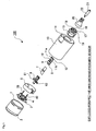
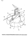
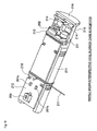
- FIG. 1 is an exploded perspective view showing a proximity sensor, to which a winding coil shield structure according to the present invention is applied.
- the proximity sensor has been previously proposed by the present applicant (see the pamphlet of WO No. 02/075,763 ), in which all of parts constituting the proximity sensor are integrated in several modules, so as to reduce the man-hours of assembly, thereby achieving the cost reduction.
- the parts of the proximity sensor are integrated in a detection end module SMJ, described later, a connecting member module CMJ, described later, and an output circuit module OMJ, described later.
- the detection end module SMJ includes a detection coil 4 wound around a spool 3 made of a resin; a ferrite core 5, in which the detection coil 4 is disposed; a coil case 1 made of a resin, for containing the detection coil 4 and the ferrite core 5 therein; and a detection circuit board 6, on which a detection circuit including an oscillation circuit having the detection coil 4 as a resonance element is mounted.
- the detection coil 4 and the detection circuit board 6 are connected to each other by soldering coil terminal pins 39 and 40 on the side of the detection coil 4 to connecting pads 61 and 62 on the side of the detection circuit board 6.
- reference numeral 2 designates a ring-like mask conductor fitted around the outer periphery at the tip of the coil case 1. As previously proposed by the present applicant, the existence of the mask conductor 2 makes the characteristics of the detection end module SMJ constant irrespective of the existence or material of a sheath case 13, thereby achieving self completion.
- the connecting member module CMJ is constituted of a harness 7 as a film-like wiring board. A plurality of wiring patterns are formed in parallel on the harness 7 along a longitudinal direction.
- the harness 7 is folded in a V shape at the intermediate portion thereof, and therefore, it can readily cope with the sheath case 13 having any length.
- the output circuit module OMJ comprises an output circuit board 8, on which an output circuit IC 9, a light emitting diode 10 and the like are mounted. At the rear end 12 of the output circuit board 8 are disposed terminal pads 11a and 11b.
- the above-described detection end module (including the coil case 1, the mask conductor 2, the spool 3, the detection coil 4, the ferrite core 5 and the detection circuit board 6) and the above-described output circuit module OMJ (including the output circuit board 8) are connected to each other via the connecting member module (including the harness 7), and are contained inside of the cylindrical sheath case 13 opened at both ends thereof. At this time, an opening at the tip of the sheath case 13 is closed since the coil case 1 is press-fitted. Furthermore, an opening at the rear end of the sheath case 13 is closed by an end plug 15.
- a slit 16 through which the rear end 12 of the output circuit board 8 projects, an injection port 17 for use in injecting a secondary injection type resin and an exhaust port 18, through which inside air is exhausted at the time of resin injection.
- an injection port 17 for use in injecting a secondary injection type resin
- an exhaust port 18 through which inside air is exhausted at the time of resin injection.
- a ridge-and-groove portion 19 for promoting fusion with a resin constituting a cord protector 20.
- the detection end module SMJ, the connecting member module CMJ and the output circuit module OMJ are contained inside of the sheath case 13.
- a pressurized fusion resin is injected through the injection port 17 in the end plug 15, thereby filling the secondary injection type resin into the clearance defined inside of the sheath case 13, so as to seal the intrusion of water or oil from the outside.
- an electric cord 21 is soldered to the terminal pads 11a and 11b at the rear end 12 of the output circuit board 8 projecting from the slit 16 formed at the end plug 15.
- the assembly is introduced into a predetermined molding die, so that the cord protector 20 is insert-molded. Consequently, the proximity sensor of a cord fixing type is completed.
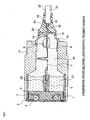
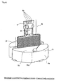
- Fig. 2 is a schematically longitudinal cross-sectional view showing the proximity sensor assembled in the above-described manner.
- reference numeral 27 designates the primary injection type resin; 28, a sealing resin for sealing the detection circuit board 6; and 29, the secondary injection type resin for sealing the clearance defined inside of the sheath case 13.
- reference numeral 21 denotes the electric cord; 22, a sheath; 23 and 24, core wires; and 25 and 26, conductors.
- the primary injection type resin 27 and the secondary injection type resin 29 are filled inside of the sheath case 13 of the proximity sensor as a complete product.
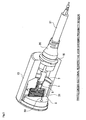
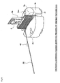
- Fig. 3 is a partly cross-sectional perspective view showing the proximity sensor in the state in which the primary injection type resin and the secondary injection type resin are removed.
- Reference numeral 31 is a planar wound portion of a coated electric wire. As described later, in the planar wound portion 31, a coated electric wire 30 is wound around a wide portion of the detection circuit board 6 in a planar manner. An electrostatic shield structure with respect to the detection circuit board 6 can be achieved by grounding the coated electric wire 30.
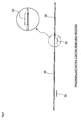
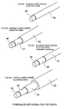
- Fig. 4 is a diagram illustrating a coating removing process. Explanation will be first made below on a preparation work for starting winding of the coated electric wire.
- the coating is fused and removed by irradiating a laser beam at two points on the coated electric wire 30, thereby forming a conductor exposed portion 32 and another conductor exposed portion 33.
- Fig. 5 work for attaching padding solders 34, 35 and 36 is performed on the side of the ferrite core 5 and the detection circuit board 6.
- the attaching position of the padding solder 34 is located at a winding starting end of the coated electric wire 30; the attaching position of the padding solder 35 is located at a winding finishing end of the coated electric wire 30; and the attaching position of the padding solder 36 is located at a terminal pad 61 on the detection circuit board 6.
- the terminal pad 61 functions as a GND pattern.
- the ferrite core 5 is formed into a thin-type cylindrical shape having an end 5a and a core circumference 5b, on which a metallic deposition film is formed.
- the padding solders 34 and 35 are attached onto the metallic deposition film.
- a welded solder 34a is formed by welding the conductor exposed portion 32 of the coated electric wire 30 to the padding solder 34 at the core end 5a of the ferrite core 5 by the irradiation of the laser beam, so that the winding starting end of the coated electric wire 30 is electrically connected to the core end of the ferrite core 5.
- the conductor exposed portion 33 of the coated electric wire 30 is located at the padding solder 36 on the detection circuit board 6 by turning the coated electric wire 30 once around the detection circuit board 6, followed by the irradiation of the laser beam, thereby forming a welded solder 36a.
- the coated electric wire 30 is grounded to the GND pattern at the welded solder 36a.
- the terminal pad 62 on the detection circuit board 6 is disposed opposite to the GND and on the side on which the terminal pad 62 is connected directly to the oscillation circuit.
- the coated electric wire 30 is started to be wound from a board edge on the side of the terminal pad 62.
- a portion to be protected most from noise is "a lead wire of a detection coil” in "a spool on the side connected to the oscillation circuit”, and therefore, the portion is wound without any clearance as possible.
- a positioning characteristic when the coated electric wire 30 is wound while being hooked at the edge of the board 6 is excellent when a hooked portion is flat, and consequently, the winding starting orientation is selected in this manner.
- the reason why the coated electric wire 30 is welded at the terminal pad 61 is that countermeasures are taken for the fear of a short-circuiting between the coated electric wire 30 and the detection circuit board 6 (which occurs by peeling-off the coating of the coated electric wire 30 by the laser or generation of the peeling-off in a length of several millimeters).
- a coil terminal pin 39 connected to the back of the terminal pad 61 is a GND terminal. Even if the coil terminal pin 39 and the coated electric wire 30 are short-circuited, there occurs no failure from the viewpoint of a circuit operation since they are GND potentials.
- the coated electric wire 30 fixed to the detection circuit board 6 via the welded solder 36a is pulled up to a shoulder 38 at an upper end in Fig. 8 at the wide portion 6a of the detection circuit board 6, and thereafter, the coated electric wire 30 is wound down from above to below, as shown in Fig. 9 .
- the coated electric wire 30 is pulled up from the welded solder 36a to the shoulder 38, and then, is pulled down. This is because a shield layer formed by the winding core should be only "a single layer". Since the clearance between the coil case 1 and the detection circuit board 6 is considerably small, if the winding coils are wound doubly or triply, the winding core shield layer may interfere at the time of insertion into the coil case 1.
- the coated electric wire 30 is wound up from below to above.
- a swelled-up portion is formed at the coil terminal pins 39 and 40 due to the connection of the coil wire and the solder, as shown in Fig. 9 , the coated electric wire 30 is slipped off due to the inclination of the swelled-up portion when the coated electric wire 30 is wound up at the swelled-up portion, thereby inducing a fear of the difficulty in winding at a uniform pitch.
- the winding coil is slipped off along the inclination from top to root at a portion at which the coated electric wire 30 is wound up in sequence from below to above, as indicated by arrows A and B in Fig.
- the coated electric wire 30 can be wound at a uniform pitch with relative ease.
- the coated electric wire 30 is wound down in sequence in a single layer from above to below around the wide portion 6a, thereby forming the planar wound portion 31. Since the planar wound portion 31 is formed of a conductor in a layered manner, it is grounded to the GND pattern at the welded solder 36a, to effectively function as an electrostatic shield member. Furthermore, the planar wound portion 31 formed in the above-described manner is insulated by the insulating coating in the direction of the adjacent coated electric wire, i.e., in a direction transverse to the coated electric wire, and therefore, no current flows.
- a conductor exposed portion 43 is formed by irradiating the laser beam onto the coated electric wire 30, to be located at the padding solder 35 at the core end 5a, and then, the conductor exposed portion 43 is welded at the core end 5a by the irradiation of the laser beam.
- the coated electric wire constituting the shield layer is electrically connected to the ferrite core at two points on the core end 5a, i.e., at the welded solders 34a and 35a.
- the coated electric wire 30 is electrically connected to the GND potential at the terminal pad 61, so that the potential of the metallic deposition film of the ferrite core 5 is stabilized at the GND potential.
- the coated electric wire 30 continuous to the conductor exposed portion 43 is cut out, thereby completing the planar wound portion 31 at which the coated electric wire is tightly wound in a planar manner around the wide portion 6a of the detection circuit board 6.
- the planar wound portion 31 is connected to the GND potential, thereby completing the electrostatic shield structure. Furthermore, since the coated electric wire 30 are connected at the two points also to the ferrite core 5, the potential of the metallic deposition film of the ferrite core 5 becomes the GND potential, thereby contributing to the operating stabilization.
- a welded point between the coated electric wire 30 and the metallic deposition film of the ferrite core 5 may be disconnected by a stress exerted at the time of the expansion or contraction during or after hardening when the primary injection type resin 29 is injected.
- the coated electric wire 30 is connected at the two points in the present preferred embodiment, the electrostatic shielding effect of the metallic deposition film can be maintained even if the coated electric wire 30 is disconnected at either one of the two points.
- the work of winding the coated electric wire around the wide portion 6a of the detection circuit board 6 can be easily automated by a coil winding machine or the like, and thus, it is possible to provide the electrostatic shield structure in the proximity sensor of this kind at a reduced cost.
- Figs. 13A to 13D illustrate examples of electric wires applicable to the shield structure in the coil according to the present invention.
- Fig. 13A illustrates a single-layer coated electric wire
- Fig. 13B illustrates a double-layer coated electric wire (a first example)
- Fig. 13C illustrates a double-layer coated electric wire (a second example)
- Fig. 13D illustrates a triple-layer coated electric wire.
- the single-layer coated electric wire includes a single copper wire 44 serving as a conductor and a polyurethane film 45.
- the coated electric wire can be used as a coil wire for a detection coil in the preferred embodiment of the above-described proximity sensor.
- the approximate thickness of the polyurethane film is 0.01 mm, and the outer diameter of the entire coated wire ranges from 0.02 mm to 0.60 mm.
- Such a single-layer coated electric wire is called a coil wire widely used in general, and is used for a relay coil, a transformer, a small-sized motor, a communication coil and the like. It is very high in versatility and is low in material cost.
- the single-layer coated electric wire is wound directly around the board, there is a fear of a damage imparted at the end edge of the board. Therefore, it is preferable that a round should be provided by covering the end edge of the board with an insulating tape or the like, and then, the single-layer coated electric wire should be wound. Otherwise, an insulating layer has been previously formed at the surface of the board.
- the insulating layer may be used a silicon potting, a cylindrical resin member, a thermally contractile tube and the like.
- the double-layer coated electric wire (the first example) illustrated in Fig. 13B includes a single copper wire 46 serving as a conductor, a first film 47 made of polyurethane and a second film 48 made of polyester.
- Each of the first film 47 and the second film 48 is an extrusion coating.
- the diameter of the conductor is 0.11 mm
- the outer diameter of the polyester film is about 0.18 mm.
- the approximate thickness of the polyurethane film is 0.01 mm and the approximate thickness of the polyester film is 0.025 mm.
- the features include a high insulating property since the double-layer insulating film has durability with respect to machining; an excellent space efficiency owing to a small sheath diameter, although the insulating property is slightly lower than the triple-layer insulating film; a material cost lower than the triple-layer coated electric wire; and the like.
- the double-layer coated electric wire (the second example) illustrated in Fig. 13C includes a single copper wire 49 serving as a conductor, a first film 50 made of polyurethane and a second film 51 made of nylon.
- the second nylon film is formed by baking a nylon resin.
- the outer diameter ranges from about 0.02 mm to about 0.55 mm.
- the approximate thickness of the polyurethane film is 0.01 mm, and the approximate thickness of the nylon film is 0.005 mm.
- the features of the coated electric wire include a low material cost because of a generally used coil wire, machining resistance, and excellent degradation characteristics.
- an edge cannot have resistance in the case where the coated electric wire is wound directly around the board. In this case, after the edge is covered with an insulating tape or the like, the coated electric wire must be wound.
- the triple-layer coated electric wire illustrated in Fig. 13D includes a single copper wire 52 serving as a conductor, a first film 53 made of polyurethane, a second film 54 made of polyester and a third film 55 made of polyamide.
- the diameter of the conductor is 0.11 mm, and the outer diameter of the polyamide film is 0.24 mm.
- the approximate thickness of the polyurethane film is 0.01 mm
- the approximate thickness of the polyester film is 0.028 mm
- the approximate thickness of the polyamide film is 0.028 mm.
- the features include resistance with respect to the edge of the board owing to the triple-layer insulting film and a sufficient insulating property.
- the detection end module in the proximity sensor is constituted by integrating the detection circuit board having the detection circuit mounted thereon, the core and the detection coil, wherein in particular, no output circuit is included in the detection circuit board.
- a board having an output circuit mounted thereon is prepared independently of the detection circuit board, and further, a plurality of kinds of detection end modules and output circuit boards are prepared. In this manner, many kinds of proximity sensor devices can be fabricated in combination.
- the detection end module may be put into circulation in a single unit as an intermediate product for the proximity sensor device.
- the electrostatic shield layer is formed by winding the coated electric wire around the detection circuit board in the detection end module, the volume of the detection end module is slightly increased, and further, the shield layer can be hardly broken at the time of handling in comparison with the winding of the film with the copper foil since the shield layer is integrated with the detection circuit board in substantial contact. Consequently, it is possible to easily handle the intermediate product of the detection end module.
- FIG. 14 is a circuit block diagram illustrating an exemplary photoelectric sensor.
- a light projecting/receiving system of the photoelectric sensor includes a light projecting element 201 constituted of an LED, a light receiving element 202 constituted of a photodiode, a light projecting circuit 203 for allowing the light projecting element 201 to emit light, and a light receiving circuit 204 for converting a current output signal from the light receiving element 202 into a voltage signal and amplifying the signal.
- the light receiving circuit 204 corresponds to the detection circuit according to the present invention.
- a central processing circuit 205 is constituted of an ASIC, controls the light projecting circuit 203 in such a manner that the light projecting element 201 is lighted at a pulse of a predetermined cycle, and further, acquires an output signal (i.e., a light receiving signal) from the light receiving circuit 204 in synchronism with a lighting timing of the light projecting element 201.
- the central processing circuit 205 has a threshold value with respect to the light receiving signal, and thus, determines a light receiving state under the condition where the magnitude of the light receiving signal exceeds the threshold value sequentially predetermined times.
- the threshold value can be adjusted by a sensitivity volume 206.
- a display lamp unit 207 includes two display lamps, i.e., an operating display lamp and a stabilizing display lamp.
- the operating display lamp is lighted when a light receiving state is determined.
- the stabilizing display lamp is lighted when a light receiving signal greater by a preset rate than the threshold value is obtained.
- An output circuit 208 converts a determination result signal into an electric signal having predetermined specifications, and then, outputs the electric signal to the outside.
- a power source circuit unit 209 receives a DC power source input within a predetermined volume range from the outside, converts the input into a voltage required inside of the sensor, and then, supplies the power source to each of the circuits.
- a coated electric wire 217 is wound around the light projecting element 201, the light receiving element 202, the light projecting circuit 203, the light receiving circuit 204, the central processing circuit 205, the output circuit 208 and the power source circuit unit 209, followed by electrostatic shielding. Only the light receiving circuit 204 may be electrostatically shielded.
- Fig. 15 is a partly broken perspective view showing the assembly of the photoelectric sensor, from which a case is removed.
- the upper half of an optical holder 210 is removed, and is shown in cross section.
- a board holder 211 is made of a resin, for holding a main circuit board 212.
- On the main circuit board 212 are mounted the circuits shown in Fig. 14 except for the light projecting element 201 and the light receiving element 202.
- the light receiving circuit 204 serving as the detection circuit and the other circuits are mounted on the main circuit board 212.
- the main circuit board 212 corresponds to the detection circuit board according to the present invention.
- reference numeral 214 designates a light projecting lens; 215, a light receiving lens; 216, a lens cover; 217, the coated electric wire; 218, a connecting portion; and 207a and 207b, display lamps constituting the display lamp unit.
- Fig. 16 illustrates the state of the assembly of the photoelectric sensor when the coated electric wire is completed to be wound, as viewed at an angle other than in Fig. 15 .
- a region denoted by reference numeral 219 is a coil shield region.
- the coated electric wire 217 is wound also around the optical holder 210 incorporating the light receiving element 202 therein.
- the terminal end of the coated electric wire 217 is securely bonded to the optical holder 210.
- a lock portion may be formed at the optical holder 210, and the coated electric wire 217 may be securely hooked on the lock portion.
- Fig. 17 illustrates the state in which the assembly of the photoelectric sensor is contained in a case 220.
- the case 220 is shown in cross section.
- the case 220 is made of a resin or metal.
- a hole 221 for operating the sensitivity volume 206 is formed at the case 220.
- a relay member, not shown, for transmitting the rotation of a driver held by an operator to the sensitivity volume 206 is inserted into the hole 221.
- Another hole 222 for visually confirming the display lamps 207a and 207b is formed at the case 220.
- a transparent window member, not shown, is fitted to the hole 222.
- a projection at the side of the board holder 211 abuts against the inner surface of the case 220.
- the board holder 211 is not a semi-split cylinder in a strict sense, but is formed into a C-shaped cylinder in cross section having an angle in excess of 180° on a center axis. Consequently, when the board holder 211 is inserted into the case 220, the board holder 211 can be held without any play inside of the case 220.
- a groove is formed at the lower surface of the board holder 211 in parallel to the center axis. The projection at the inner surface of the case is inserted into the groove, so that the board holder 211 is prevented from being turned with respect to the case 220.
- the board holder 211 can be positioned with respect to the case 220 only by inserting the board holder 211 into the case 220 from the front of the case 220. Additionally, since the shape of the board holder 211 is substantially half-split cylinder with few irregular portion, the coated electric wire 217 can be easily wound in alignment.
- the above-described photoelectric sensor further has a cap structure at the rear end of the case and a cable drawing structure. However, their illustrations and explanations will be omitted here.
Description
- The present invention relates to a sensor device, in which a detection circuit is electrostatically shielded.
- In a proximity sensor of an induction type, there has been known that an insulating flexible film having a conductor pattern is wound around a printed wiring board having a circuit unit mounted thereon, so that the printed wiring board is electrostatically shielded, and further, that the conductor pattern is soldered to a deposition film formed at the back surface of a core (see
Patent Literature 1 which is Japanese Patent Application Laid-open No.1,436/1981 DE 30 14 416 A1DE 30 14 416 A1claim 1. - Furthermore, there has been known that in a coil device, in which a coil wire is applied to a magnetic core, a fine wire of a metallic magnet such as permalloy or silicon steel is wound around the coil wire, so that the coil wire is magnetically shielded (see
Patent Literature 2 which is Japanese Patent Application Laid-open No.195,542/1999 - The proximity switch which adopts the electrostatic shield structure disclosed in
Patent Literature 1 has raised problems that: a film with a copper foil, which is subjected to secondary machining in a complicated shape and is expensive in material cost, is needed in each kind of sensor; it is cumbersome to manually wind the film with a copper foil having a complicated shape around the circuit board, thereby increasing the man-hours of assembly; it is difficult to automatically wind the film with a copper foil having a complicated shape around a circuit board; the man-hours of soldering a copper foil portion of the film with a copper foil to a GND pattern of the circuit board is large; it is difficult to automatically solder the copper foil portion of the film with a copper foil to the GND pattern of the circuit board; a film with a complicated electrostatic shield copper foil is needed by disposing a lead wire or a welded portion for electrically welding the metallic deposition portion of the core to the GND pattern of the circuit board; it is difficult to automatically solder the metallic deposition portion of the core and the GND pattern of the circuit board to each other by the use of the lead wire or the film with a copper foil; it is necessary to apply an insulating layer to the surface of the film with a copper foil in order to secure an insulating property between electronic parts or a sheath case, thereby requiring the film with a copper foil excellent in material cost; the surface of the insulating layer is peeled off when the insulating layer scrapes on the edge of the circuit board or the like since the insulating layer is relatively thin, thereby inducing short-circuiting between the electronic parts or circuit patterns; and the like. - The shield structure disclosed in
Patent Literature 2 has not been suitable for electrostatically shielding a detection circuit in a sensor device since a member to be shielded is not a circuit board but a coil and a magnetic material wire is thickly wound for the purpose of magnetic shielding. -
GB-1 280 289 A - In view of the above-described problems observed in the prior art, an object of the present invention is to provide a sensor device capable of electrostatically shielding a detection circuit with ease.
- Other objects, functions and effects of the present invention will be readily understood by one skilled in the art in consideration of the description below in the specification.
- The invention is as defined in
claim 1. - In a sensor device according to the present invention, a coated electric wire is wound around a detection circuit in a planar manner for the purpose of electrostatic shield.
- With the above-described configuration, since there is formed a conductor layer having the coated electric wire wound in a planar manner around the detection circuit, which is generally susceptible to an influence of noise in the sensor device, the detection circuit can be electrostatically shielded by stabilizing the potential of the coated electric wire via grounding at an intermediate portion thereof. Since the electrostatic shielding is directed, it is preferable that the material of a core wire of the coated electric wire should be low in electric resistance such as copper without any necessity of inclusion of a magnetic material. The detection circuit may be mounted on a circuit board, or may be a simple introducing-out path for an output signal in a transducer for converting a physical quantity into an electric signal, for example, a metallic lead frame.
- Since the electrostatic shielding is directed, it is sufficient that the coated electric wire is thinly wound. For example, the coated electric wire may be spirally wound around the detection circuit in a single manner. In this manner, it is easy to miniaturize the sensor device because the thickness of a shield layer can be miniaturized while achieving the effect of the electrostatic shielding.
- The sensor device comprises a detection circuit board having the detection circuit; and a cylindrical case. The coated electric wire is wound around the detection circuit board in a cylindrical manner, and the direction of an axis of the cylindrical surface accords with the direction of the axis of the case. With this configuration, the space defined inside of the case can be effectively used.
- The sensor device is a proximity sensor device comprising a detection coil having a core, wherein the detection circuit includes an oscillation circuit having the detection coil serving as a resonance element. The proximity sensor device includes a product called a proximity switch.
- In the proximity switch according to the present invention, a metallic film for electrostatically shielding the detection coil is formed at the outer surface of the core, and the coated electric wire is electrically connected to the metallic film of the core. In this manner, the detection coil also can be electrostatically shielded.
- There is provided a detection circuit board having the detection circuit; wherein both ends of the coated electric wire are electrically connected to the metallic film of the core, and are electrically connected to a ground pattern of the detection circuit board at an intermediate portion of the coated electric wire by means of a welded solder. A stress of a filled resin is liable to be exerted on the connected portion between the coated electric wire and the metallic film of the core. Consequently, if both ends of the coated electric wire are connected, the electrostatic shielding with respect to the detection coil can be maintained even if one of both ends is disconnected.
- In the coil wire of the detection coil in the proximity sensor device, a high coating strength is not required, although the high density of the core wire at the time of winding is required. In contrast, in the coated electric wire wound around the detection circuit, unintended electric short-circuiting with the detection circuit must be prevented, although the high density of the core wire at the time of winding is not required. Therefore, it is preferable that the coating strength of the coated electric wire for use in shielding should be greater than that of the coated electric wire to be used as a coil wire of the detection coil.
- However, in the case where there is no possibility of short-circuiting between the coated electric wire and the detection circuit, the coated electric wire for use in shielding may be the same kind of coated electric wire to be used as a coil wire of the detection coil. In this manner, it is possible to facilitate a fabricating process.
- An exemplary sensor device is a photoelectric sensor device including a light receiving element for converting light from a region to be detected into an electric signal, wherein a signal relating to the state of the region to be detected is output based on an output from the light receiving element. The photoelectric sensor device includes products called an photoelectric switch, a photomicro sensor and a photomicro switch. The detection circuit in the photoelectric sensor device may be a simple introducing-out path of an output signal from a light receiving element, but in many cases, it includes a light receiving circuit for amplifying the output signal from the light receiving element. In the case where there is a determination circuit for determining an object to be detected based on the output signal from the light receiving circuit, the determination circuit may be electrostatically shielded. In the case of an photoelectric sensor device further comprising a light projecting element, a light projecting circuit for allowing the light projecting element to emit light, and a central processing circuit for controlling the light projecting circuit and determining the object to be detected based on the output signal from the light receiving circuit, the central processing circuit may be electrostatically shielded.
- In the photoelectric sensor device, the coated electric wire may be wound also around the light receiving element in a planar manner. In this manner, not only the detection circuit but also the light receiving element can be electrostatically shielded in the process of winding the coated electric wire.
- In the photoelectric sensor device, there are further provided a detection circuit board having the detection circuit; a cylindrical case; and a semi-split cylindrical board holder which supports the detection circuit board and is contained inside of the case; wherein the coated electric wire is wound around the detection circuit board and the board holder in a planar manner. The coated electric wire may be wound around the light receiving element in a planar manner.
- According to the present invention, it is possible to electrostatically shield the detection circuit in the sensor device according to
claim 1 with ease. -
-
Fig. 1 is an exploded perspective view showing a proximity sensor. -
Fig. 2 is a longitudinal cross-sectional view showing the proximity sensor. -
Fig. 3 is a partly cross-sectional perspective view showing the proximity sensor. -
Fig. 4 is a diagram illustrating a coating removing process. -
Fig. 5 is a diagram illustrating a solder bonding process. -
Fig. 6 is a diagram illustrating a welding process to a core at the beginning of winding. -
Fig. 7 is a diagram illustrating the welding process to a board at the time of one turn winding. -
Fig. 8 is a diagram illustrating a transferring process to the upper end of a board. -
Fig. 9 is a diagram illustrating a winding-down starting process. -
Fig. 10 is a diagram illustrating a winding-down completing process. -
Fig. 11 is a diagram illustrating a coating removing process of a winding finishing end. -
Fig. 12 is a diagram illustrating the welding process to the core at the time of winding completion. -
Figs. 13A to 13D illustrate examples of applicable electric wires. -
Fig. 14 is a circuit block diagram illustrating an photoelectric sensor. -
Fig. 15 is a partly broken perspective view showing the assembly of the photoelectric sensor, from which a case is removed. -
Fig. 16 is a perspective view showing the assembly of the photoelectric sensor in the state in which the coated electric wire is completed to be wound. -
Fig. 17 is a partly broken perspective view showing the assembly of the photoelectric sensor, which is contained in the case. - A proximity sensor in a preferred embodiment according to the present invention will be described below in reference to the accompanying drawings.
Fig. 1 is an exploded perspective view showing a proximity sensor, to which a winding coil shield structure according to the present invention is applied. Incidentally, the proximity sensor has been previously proposed by the present applicant (see the pamphlet ofWO No. 02/075,763 - That is to say, the parts of the proximity sensor are integrated in a detection end module SMJ, described later, a connecting member module CMJ, described later, and an output circuit module OMJ, described later.
- Explanation will be made on the detection end module SMJ. The detection end module SMJ includes a
detection coil 4 wound around aspool 3 made of a resin; aferrite core 5, in which thedetection coil 4 is disposed; acoil case 1 made of a resin, for containing thedetection coil 4 and theferrite core 5 therein; and adetection circuit board 6, on which a detection circuit including an oscillation circuit having thedetection coil 4 as a resonance element is mounted. Thedetection coil 4 and thedetection circuit board 6 are connected to each other by soldering coil terminal pins 39 and 40 on the side of thedetection coil 4 to connectingpads detection circuit board 6. The assembly consisting of thespool 3 having thedetection coil 4 wound therearound, theferrite core 5 and thedetection circuit board 6 in an integral manner is contained inside of thecoil case 1 made of a resin, and thereafter, a primary injection type resin is filled in thecoil case 1. Here,reference numeral 2 designates a ring-like mask conductor fitted around the outer periphery at the tip of thecoil case 1. As previously proposed by the present applicant, the existence of themask conductor 2 makes the characteristics of the detection end module SMJ constant irrespective of the existence or material of asheath case 13, thereby achieving self completion. - Next, a description will be given of the connecting member module CMJ. The connecting member module CMJ is constituted of a
harness 7 as a film-like wiring board. A plurality of wiring patterns are formed in parallel on theharness 7 along a longitudinal direction. Theharness 7 is folded in a V shape at the intermediate portion thereof, and therefore, it can readily cope with thesheath case 13 having any length. - Subsequently, explanation will be made on the output circuit module OMJ. The output circuit module OMJ comprises an
output circuit board 8, on which anoutput circuit IC 9, alight emitting diode 10 and the like are mounted. At therear end 12 of theoutput circuit board 8 are disposedterminal pads - The above-described detection end module (including the
coil case 1, themask conductor 2, thespool 3, thedetection coil 4, theferrite core 5 and the detection circuit board 6) and the above-described output circuit module OMJ (including the output circuit board 8) are connected to each other via the connecting member module (including the harness 7), and are contained inside of thecylindrical sheath case 13 opened at both ends thereof. At this time, an opening at the tip of thesheath case 13 is closed since thecoil case 1 is press-fitted. Furthermore, an opening at the rear end of thesheath case 13 is closed by anend plug 15. At the rear end of theend plug 15 are formed aslit 16, through which therear end 12 of theoutput circuit board 8 projects, aninjection port 17 for use in injecting a secondary injection type resin and anexhaust port 18, through which inside air is exhausted at the time of resin injection. At the outer periphery at the rear end of theexhaust port 18 is formed a ridge-and-groove portion 19 for promoting fusion with a resin constituting acord protector 20. - The detection end module SMJ, the connecting member module CMJ and the output circuit module OMJ are contained inside of the
sheath case 13. After the rear opening of thesheath case 13 is closed by theend plug 15, a pressurized fusion resin is injected through theinjection port 17 in theend plug 15, thereby filling the secondary injection type resin into the clearance defined inside of thesheath case 13, so as to seal the intrusion of water or oil from the outside. Thereafter, anelectric cord 21 is soldered to theterminal pads rear end 12 of theoutput circuit board 8 projecting from theslit 16 formed at theend plug 15. Subsequently, the assembly is introduced into a predetermined molding die, so that thecord protector 20 is insert-molded. Consequently, the proximity sensor of a cord fixing type is completed. -
Fig. 2 is a schematically longitudinal cross-sectional view showing the proximity sensor assembled in the above-described manner. InFig. 2 ,reference numeral 27 designates the primary injection type resin; 28, a sealing resin for sealing thedetection circuit board 6; and 29, the secondary injection type resin for sealing the clearance defined inside of thesheath case 13. Furthermore,reference numeral 21 denotes the electric cord; 22, a sheath; 23 and 24, core wires; and 25 and 26, conductors. - Inside of the
sheath case 13 of the proximity sensor as a complete product are filled the primaryinjection type resin 27 and the secondaryinjection type resin 29. - Next,
Fig. 3 is a partly cross-sectional perspective view showing the proximity sensor in the state in which the primary injection type resin and the secondary injection type resin are removed.Reference numeral 31 is a planar wound portion of a coated electric wire. As described later, in theplanar wound portion 31, a coatedelectric wire 30 is wound around a wide portion of thedetection circuit board 6 in a planar manner. An electrostatic shield structure with respect to thedetection circuit board 6 can be achieved by grounding the coatedelectric wire 30. - Subsequently, the producing procedures of the
planar wound portion 31 will be explained below in reference toFigs. 4 to 12 . -
Fig. 4 is a diagram illustrating a coating removing process. Explanation will be first made below on a preparation work for starting winding of the coated electric wire. In the preparation step, as shown inFig. 4 , the coating is fused and removed by irradiating a laser beam at two points on the coatedelectric wire 30, thereby forming a conductor exposedportion 32 and another conductor exposedportion 33. In the meantime, as shown inFig. 5 , work for attaching padding solders 34, 35 and 36 is performed on the side of theferrite core 5 and thedetection circuit board 6. Here, the attaching position of thepadding solder 34 is located at a winding starting end of the coatedelectric wire 30; the attaching position of thepadding solder 35 is located at a winding finishing end of the coatedelectric wire 30; and the attaching position of thepadding solder 36 is located at aterminal pad 61 on thedetection circuit board 6. Theterminal pad 61 functions as a GND pattern. Incidentally, theferrite core 5 is formed into a thin-type cylindrical shape having anend 5a and acore circumference 5b, on which a metallic deposition film is formed. The padding solders 34 and 35 are attached onto the metallic deposition film. - Subsequently, as shown in
Fig. 6 , a weldedsolder 34a is formed by welding the conductor exposedportion 32 of the coatedelectric wire 30 to thepadding solder 34 at thecore end 5a of theferrite core 5 by the irradiation of the laser beam, so that the winding starting end of the coatedelectric wire 30 is electrically connected to the core end of theferrite core 5. - Next, as shown in
Fig. 7 , the conductor exposedportion 33 of the coatedelectric wire 30 is located at thepadding solder 36 on thedetection circuit board 6 by turning the coatedelectric wire 30 once around thedetection circuit board 6, followed by the irradiation of the laser beam, thereby forming a weldedsolder 36a. As described above, since theterminal pad 61 having thepadding solder 36 attached thereto functions as the GND pattern, the coatedelectric wire 30 is grounded to the GND pattern at the weldedsolder 36a. - The
terminal pad 62 on thedetection circuit board 6 is disposed opposite to the GND and on the side on which theterminal pad 62 is connected directly to the oscillation circuit. As shown inFig. 6 , after the coatedelectric wire 30 is fixed at thecore end 5a via the weldedsolder 34, the coatedelectric wire 30 is started to be wound from a board edge on the side of theterminal pad 62. This is because a portion to be protected most from noise is "a lead wire of a detection coil" in "a spool on the side connected to the oscillation circuit", and therefore, the portion is wound without any clearance as possible. A positioning characteristic when the coatedelectric wire 30 is wound while being hooked at the edge of theboard 6 is excellent when a hooked portion is flat, and consequently, the winding starting orientation is selected in this manner. - The reason why the coated
electric wire 30 is welded at theterminal pad 61 is that countermeasures are taken for the fear of a short-circuiting between the coatedelectric wire 30 and the detection circuit board 6 (which occurs by peeling-off the coating of the coatedelectric wire 30 by the laser or generation of the peeling-off in a length of several millimeters). Specifically, acoil terminal pin 39 connected to the back of theterminal pad 61 is a GND terminal. Even if thecoil terminal pin 39 and the coatedelectric wire 30 are short-circuited, there occurs no failure from the viewpoint of a circuit operation since they are GND potentials. - Subsequently, as shown in
Fig. 8 , the coatedelectric wire 30 fixed to thedetection circuit board 6 via the weldedsolder 36a is pulled up to ashoulder 38 at an upper end inFig. 8 at thewide portion 6a of thedetection circuit board 6, and thereafter, the coatedelectric wire 30 is wound down from above to below, as shown inFig. 9 . Here, as shown inFigs. 8 and9 , the coatedelectric wire 30 is pulled up from the weldedsolder 36a to theshoulder 38, and then, is pulled down. This is because a shield layer formed by the winding core should be only "a single layer". Since the clearance between thecoil case 1 and thedetection circuit board 6 is considerably small, if the winding coils are wound doubly or triply, the winding core shield layer may interfere at the time of insertion into thecoil case 1. - Incidentally, there also is construed that the coated
electric wire 30 is wound up from below to above. However, since a swelled-up portion is formed at the coil terminal pins 39 and 40 due to the connection of the coil wire and the solder, as shown inFig. 9 , the coatedelectric wire 30 is slipped off due to the inclination of the swelled-up portion when the coatedelectric wire 30 is wound up at the swelled-up portion, thereby inducing a fear of the difficulty in winding at a uniform pitch. Actually, the winding coil is slipped off along the inclination from top to root at a portion at which the coatedelectric wire 30 is wound up in sequence from below to above, as indicated by arrows A and B inFig. 9 , thereby resulting in the relative difficulty in uniformly winding. In contrast, in the case where the coatedelectric wire 30 is wound down in sequence from above to below, as shown inFigs. 9 and10 , the coatedelectric wire 30 can be wound at a uniform pitch with relative ease. - Thereafter, as shown in
Fig. 10 , the coatedelectric wire 30 is wound down in sequence in a single layer from above to below around thewide portion 6a, thereby forming theplanar wound portion 31. Since theplanar wound portion 31 is formed of a conductor in a layered manner, it is grounded to the GND pattern at the weldedsolder 36a, to effectively function as an electrostatic shield member. Furthermore, theplanar wound portion 31 formed in the above-described manner is insulated by the insulating coating in the direction of the adjacent coated electric wire, i.e., in a direction transverse to the coated electric wire, and therefore, no current flows. And then, even if a high frequency magnetic field generated from thedetection coil 4 travels transversely to theplanar wound portion 31 to thus generate an eddy current electromotive force, no eddy current flows in a direction transverse to the winding coil. Consequently, an eddy current loss hardly occurs, thus avoiding any degradation of the characteristics of the proximity sensor. - Finally, as shown in
Figs. 11 and12 , a conductor exposedportion 43 is formed by irradiating the laser beam onto the coatedelectric wire 30, to be located at thepadding solder 35 at thecore end 5a, and then, the conductor exposedportion 43 is welded at thecore end 5a by the irradiation of the laser beam. In this manner, as shown inFig. 12 , the coated electric wire constituting the shield layer is electrically connected to the ferrite core at two points on thecore end 5a, i.e., at the weldedsolders electric wire 30 is electrically connected to the GND potential at theterminal pad 61, so that the potential of the metallic deposition film of theferrite core 5 is stabilized at the GND potential. - Thereafter, as shown in
Fig. 12 , the coatedelectric wire 30 continuous to the conductor exposedportion 43 is cut out, thereby completing theplanar wound portion 31 at which the coated electric wire is tightly wound in a planar manner around thewide portion 6a of thedetection circuit board 6. Theplanar wound portion 31 is connected to the GND potential, thereby completing the electrostatic shield structure. Furthermore, since the coatedelectric wire 30 are connected at the two points also to theferrite core 5, the potential of the metallic deposition film of theferrite core 5 becomes the GND potential, thereby contributing to the operating stabilization. A welded point between the coatedelectric wire 30 and the metallic deposition film of theferrite core 5 may be disconnected by a stress exerted at the time of the expansion or contraction during or after hardening when the primaryinjection type resin 29 is injected. However, the coatedelectric wire 30 is connected at the two points in the present preferred embodiment, the electrostatic shielding effect of the metallic deposition film can be maintained even if the coatedelectric wire 30 is disconnected at either one of the two points. - Additionally, the work of winding the coated electric wire around the
wide portion 6a of thedetection circuit board 6 can be easily automated by a coil winding machine or the like, and thus, it is possible to provide the electrostatic shield structure in the proximity sensor of this kind at a reduced cost. - Next,
Figs. 13A to 13D illustrate examples of electric wires applicable to the shield structure in the coil according to the present invention.Fig. 13A illustrates a single-layer coated electric wire;Fig. 13B illustrates a double-layer coated electric wire (a first example);Fig. 13C illustrates a double-layer coated electric wire (a second example); andFig. 13D illustrates a triple-layer coated electric wire. - As illustrated in
Fig. 13A , the single-layer coated electric wire includes asingle copper wire 44 serving as a conductor and apolyurethane film 45. The coated electric wire can be used as a coil wire for a detection coil in the preferred embodiment of the above-described proximity sensor. The approximate thickness of the polyurethane film is 0.01 mm, and the outer diameter of the entire coated wire ranges from 0.02 mm to 0.60 mm. Such a single-layer coated electric wire is called a coil wire widely used in general, and is used for a relay coil, a transformer, a small-sized motor, a communication coil and the like. It is very high in versatility and is low in material cost. However, in the case where the single-layer coated electric wire is wound directly around the board, there is a fear of a damage imparted at the end edge of the board. Therefore, it is preferable that a round should be provided by covering the end edge of the board with an insulating tape or the like, and then, the single-layer coated electric wire should be wound. Otherwise, an insulating layer has been previously formed at the surface of the board. As the insulating layer may be used a silicon potting, a cylindrical resin member, a thermally contractile tube and the like. - The double-layer coated electric wire (the first example) illustrated in
Fig. 13B includes asingle copper wire 46 serving as a conductor, afirst film 47 made of polyurethane and asecond film 48 made of polyester. Each of thefirst film 47 and thesecond film 48 is an extrusion coating. In the case where a finest wire is selected, the diameter of the conductor is 0.11 mm, and the outer diameter of the polyester film is about 0.18 mm. In the case where the diameter of the conductor is 0.11 mm, the approximate thickness of the polyurethane film is 0.01 mm and the approximate thickness of the polyester film is 0.025 mm. - The features include a high insulating property since the double-layer insulating film has durability with respect to machining; an excellent space efficiency owing to a small sheath diameter, although the insulating property is slightly lower than the triple-layer insulating film; a material cost lower than the triple-layer coated electric wire; and the like.
- The double-layer coated electric wire (the second example) illustrated in
Fig. 13C includes asingle copper wire 49 serving as a conductor, afirst film 50 made of polyurethane and asecond film 51 made of nylon. The second nylon film is formed by baking a nylon resin. The outer diameter ranges from about 0.02 mm to about 0.55 mm. The approximate thickness of the polyurethane film is 0.01 mm, and the approximate thickness of the nylon film is 0.005 mm. - The features of the coated electric wire include a low material cost because of a generally used coil wire, machining resistance, and excellent degradation characteristics. However, an edge cannot have resistance in the case where the coated electric wire is wound directly around the board. In this case, after the edge is covered with an insulating tape or the like, the coated electric wire must be wound.
- The triple-layer coated electric wire illustrated in
Fig. 13D includes asingle copper wire 52 serving as a conductor, afirst film 53 made of polyurethane, asecond film 54 made of polyester and athird film 55 made of polyamide. The diameter of the conductor is 0.11 mm, and the outer diameter of the polyamide film is 0.24 mm. In the case where the diameter of the conductor is 0.11 mm, the approximate thickness of the polyurethane film is 0.01 mm, the approximate thickness of the polyester film is 0.028 mm and the approximate thickness of the polyamide film is 0.028 mm. - The features include resistance with respect to the edge of the board owing to the triple-layer insulting film and a sufficient insulating property.
- In the above-described preferred embodiment, there can be produced the following effects.
- (1) Since the shield unit is constituted of the coated electric wire which is inexpensive in material cost, a remarkable cost reduction can be expected.
- (2) Since the shield unit is constituted by winding the coated electric wire around the circuit board, only a single kind of coated electric wire can cope with products of various sizes. Consequently, the shield members need not be prepared for each kind of products, thereby facilitating the management of members.
- (3) Since the shield unit is constituted by winding the coated electric wire around the circuit board, the assembling automation can be achieved with ease by the use of a winding machine.
- (4) A lead wire or a copper foil for welding the metallic deposition portion of the coil core to the GND of the circuit board is not needed, thereby achieving reduction of the material cost.
- (5) The automation of electric welding of the shield unit to the GND of the circuit board can be achieved with ease.
- (6) The automation of electric welding of the metallic deposition portion of the coil core to the GND of the circuit board can be achieved with ease.
- (7) Since the coated electric wire is wound on the electronic part mounted on the circuit board, the electronic part can be protected from the outside. Consequently, it is possible to alleviate the exertion of the stress of the injection type resin on the electronic part, so as to prevent any peeling-off or crack of the electronic part.
- (8) In the case of the common use as the coated wire for the detection coil, the same material can be used as the wire rod for the detection coil and the shield unit, thereby integrating the members so as to achieve stock control and reduce the cost.
- (9) In the case where the same material is used by the common use of the detection coil, the same equipment is used in the process of winding the detection coil and in the process of winding the shield, thereby reducing the equipment cost and the number of processes.
- (10) Since the shield unit which can be fitted to the circuit board or the electronic part having the coated electric wire wound therearound can be constituted, the mounting efficiency is excellent without any necessity of previous provision of an extra space in comparison with the planar winding with the film with the copper foil in the prior art.
- The detection end module in the proximity sensor is constituted by integrating the detection circuit board having the detection circuit mounted thereon, the core and the detection coil, wherein in particular, no output circuit is included in the detection circuit board. A board having an output circuit mounted thereon is prepared independently of the detection circuit board, and further, a plurality of kinds of detection end modules and output circuit boards are prepared. In this manner, many kinds of proximity sensor devices can be fabricated in combination. The detection end module may be put into circulation in a single unit as an intermediate product for the proximity sensor device. If the electrostatic shield layer is formed by winding the coated electric wire around the detection circuit board in the detection end module, the volume of the detection end module is slightly increased, and further, the shield layer can be hardly broken at the time of handling in comparison with the winding of the film with the copper foil since the shield layer is integrated with the detection circuit board in substantial contact. Consequently, it is possible to easily handle the intermediate product of the detection end module.
- Next,
Fig. 14 is a circuit block diagram illustrating an exemplary photoelectric sensor. A light projecting/receiving system of the photoelectric sensor includes alight projecting element 201 constituted of an LED, alight receiving element 202 constituted of a photodiode, alight projecting circuit 203 for allowing thelight projecting element 201 to emit light, and alight receiving circuit 204 for converting a current output signal from thelight receiving element 202 into a voltage signal and amplifying the signal. In the present exemplary embodiment, thelight receiving circuit 204 corresponds to the detection circuit according to the present invention. - A
central processing circuit 205 is constituted of an ASIC, controls thelight projecting circuit 203 in such a manner that thelight projecting element 201 is lighted at a pulse of a predetermined cycle, and further, acquires an output signal (i.e., a light receiving signal) from thelight receiving circuit 204 in synchronism with a lighting timing of thelight projecting element 201. Moreover, thecentral processing circuit 205 has a threshold value with respect to the light receiving signal, and thus, determines a light receiving state under the condition where the magnitude of the light receiving signal exceeds the threshold value sequentially predetermined times. The threshold value can be adjusted by asensitivity volume 206. Adisplay lamp unit 207 includes two display lamps, i.e., an operating display lamp and a stabilizing display lamp. The operating display lamp is lighted when a light receiving state is determined. The stabilizing display lamp is lighted when a light receiving signal greater by a preset rate than the threshold value is obtained. Anoutput circuit 208 converts a determination result signal into an electric signal having predetermined specifications, and then, outputs the electric signal to the outside. A powersource circuit unit 209 receives a DC power source input within a predetermined volume range from the outside, converts the input into a voltage required inside of the sensor, and then, supplies the power source to each of the circuits. - In the present exemplary embodiment, a coated
electric wire 217 is wound around thelight projecting element 201, thelight receiving element 202, thelight projecting circuit 203, thelight receiving circuit 204, thecentral processing circuit 205, theoutput circuit 208 and the powersource circuit unit 209, followed by electrostatic shielding. Only thelight receiving circuit 204 may be electrostatically shielded. -
Fig. 15 is a partly broken perspective view showing the assembly of the photoelectric sensor, from which a case is removed. InFig. 15 , the upper half of anoptical holder 210 is removed, and is shown in cross section. InFig. 15 , aboard holder 211 is made of a resin, for holding amain circuit board 212. On themain circuit board 212 are mounted the circuits shown inFig. 14 except for thelight projecting element 201 and thelight receiving element 202. In this manner, thelight receiving circuit 204 serving as the detection circuit and the other circuits are mounted on themain circuit board 212. Here, themain circuit board 212 corresponds to the detection circuit board according to the present invention. Signals are transmitted between the light projectingelement 201 and themain circuit board 212 and between thelight receiving element 202 and themain circuit board 212 via a light projecting/receivingelement board 213. In addition, inFig. 15 ,reference numeral 214 designates a light projecting lens; 215, a light receiving lens; 216, a lens cover; 217, the coated electric wire; 218, a connecting portion; and 207a and 207b, display lamps constituting the display lamp unit. -
Fig. 16 illustrates the state of the assembly of the photoelectric sensor when the coated electric wire is completed to be wound, as viewed at an angle other than inFig. 15 . A region denoted byreference numeral 219 is a coil shield region. As is clear fromFig. 16 , the coatedelectric wire 217 is wound also around theoptical holder 210 incorporating thelight receiving element 202 therein. The terminal end of the coatedelectric wire 217 is securely bonded to theoptical holder 210. Here, a lock portion may be formed at theoptical holder 210, and the coatedelectric wire 217 may be securely hooked on the lock portion. -
Fig. 17 illustrates the state in which the assembly of the photoelectric sensor is contained in acase 220. In the present exemplary embodiment, thecase 220 is shown in cross section. Thecase 220 is made of a resin or metal. Ahole 221 for operating thesensitivity volume 206 is formed at thecase 220. A relay member, not shown, for transmitting the rotation of a driver held by an operator to thesensitivity volume 206 is inserted into thehole 221. Anotherhole 222 for visually confirming thedisplay lamps case 220. A transparent window member, not shown, is fitted to thehole 222. - A projection at the side of the
board holder 211 abuts against the inner surface of thecase 220. Theboard holder 211 is not a semi-split cylinder in a strict sense, but is formed into a C-shaped cylinder in cross section having an angle in excess of 180° on a center axis. Consequently, when theboard holder 211 is inserted into thecase 220, theboard holder 211 can be held without any play inside of thecase 220. Moreover, a groove is formed at the lower surface of theboard holder 211 in parallel to the center axis. The projection at the inner surface of the case is inserted into the groove, so that theboard holder 211 is prevented from being turned with respect to thecase 220. With the above-described structure, theboard holder 211 can be positioned with respect to thecase 220 only by inserting theboard holder 211 into thecase 220 from the front of thecase 220. Additionally, since the shape of theboard holder 211 is substantially half-split cylinder with few irregular portion, the coatedelectric wire 217 can be easily wound in alignment. There is no interference disturbing the winding in alignment of the coatedelectric wire 217 at a surface on a side in contact with the coatedelectric wire 217 in themain circuit board 212 if parts are mounted only at a surface on a side of theboard holder 211 at a portion of themain circuit board 212 to be wound with the coatedelectric wire 217, so that the coatedelectric wire 217 can be more easily wound in alignment, and further, a fear of short-circuiting between the coatedelectric wire 217 and the circuit can be more reduced. The above-described photoelectric sensor further has a cap structure at the rear end of the case and a cable drawing structure. However, their illustrations and explanations will be omitted here.
Claims (3)
- A proximity sensor device comprising:a detection coil (4) having a core (5), a metallic film for electrostatically shielding the detection coil (4) being formed at the outer surface of the core (5);a detection circuit board (6, 212) having a detection circuit, the detection circuit including an oscillation circuit having the detection coil (4) serving as a resonance element;and a cylindrical case (1, 220), characterized bya coated electric wire (30, 217) wound around the detection circuit so as to electrostatically shield the detection circuit;wherein the coated electric wire (30, 217) is wound around the detection circuit board in a cylindrical manner so as to form a cylindrical surface, the direction of an axis of the cylindrical surface according with the direction of the axis of the case (220), and the coated electric wire (217) being electrically connected to the metallic film of the core,wherein both ends of the coated electric wire (217) are electrically connected to the metallic film of the core (5), and are electrically connected to a ground pattern of the detection circuit board (212) at an intermediate portion of the coated electric wire (217) by means of a welded solder (36a).
- The sensor device according to claim 1, wherein the coating strength of the coated electric wire (217) for use in shielding is greater than that of the coated electric wire to be used as a coil wire of the detection coil (4).
- The sensor device according to claim 1, wherein the coated electric wire (217) for use in shielding is the same kind of coated electric wire to be used as a coil wire of the detection coil.
Applications Claiming Priority (2)
| Application Number | Priority Date | Filing Date | Title |
|---|---|---|---|
| JP2002320460 | 2002-11-01 | ||
| JP2002320460 | 2002-11-01 |
Publications (3)
| Publication Number | Publication Date |
|---|---|
| EP1416635A2 EP1416635A2 (en) | 2004-05-06 |
| EP1416635A3 EP1416635A3 (en) | 2006-05-24 |
| EP1416635B1 true EP1416635B1 (en) | 2012-12-12 |
Family
ID=32089628
Family Applications (1)
| Application Number | Title | Priority Date | Filing Date |
|---|---|---|---|
| EP03024962A Expired - Lifetime EP1416635B1 (en) | 2002-11-01 | 2003-10-29 | Sensor device |
Country Status (3)
| Country | Link |
|---|---|
| US (1) | US7145348B2 (en) |
| EP (1) | EP1416635B1 (en) |
| CN (1) | CN100409734C (en) |
Families Citing this family (19)
| Publication number | Priority date | Publication date | Assignee | Title |
|---|---|---|---|---|
| DE20211087U1 (en) * | 2002-07-23 | 2003-12-04 | Werner Turck Gmbh & Co. Kg | Proximity switch with shielding encapsulated in a plastic housing |
| DE102005041112A1 (en) * | 2005-08-30 | 2007-03-01 | BSH Bosch und Siemens Hausgeräte GmbH | Capacitive proximity switch for e.g. washing machine, has sensor surface with active shielding formed by shielding surface, and clock signal applied at shielding surface that is connected with earth for applying potential by switch |
| DE102005041109A1 (en) * | 2005-08-30 | 2007-03-01 | BSH Bosch und Siemens Hausgeräte GmbH | Capacitive proximity switch for use in input field of e.g. washing machine, has electronic components of evaluation circuit arranged on support such that they protrude into cavity, which is surrounded by electrically-conducting body |
| DE102007042592A1 (en) * | 2007-09-07 | 2009-03-26 | Siemens Medical Instruments Pte. Ltd. | Transmission device for a hearing device with foil conductor shield and self-shielded coil |
| US8502151B2 (en) * | 2010-01-31 | 2013-08-06 | Avago Technologies General Ip (Singapore) Pte. Ltd. | Optical proximity sensor package with lead frame |
| EP2741419B1 (en) * | 2012-12-10 | 2015-01-21 | ifm electronic gmbh | Inductive proximity switch |
| CN108352102B (en) * | 2015-11-19 | 2020-02-14 | 法国圣戈班玻璃厂 | Alarm glass plate device |
| DE102016211004A1 (en) * | 2016-06-21 | 2017-12-21 | Zf Friedrichshafen Ag | Method for producing a sensor system with two inductive sensors |
| JP2019531533A (en) | 2016-08-02 | 2019-10-31 | サン−ゴバン グラス フランス | Alarm pane assembly |
| KR20190037281A (en) | 2016-08-02 | 2019-04-05 | 쌩-고벵 글래스 프랑스 | Alarm plate glass assembly |
| KR102143853B1 (en) * | 2016-09-28 | 2020-08-12 | 에스엠시 가부시키가이샤 | Position detection switch and its manufacturing method |
| JP6968545B2 (en) * | 2017-02-01 | 2021-11-17 | オムロン株式会社 | Proximity sensor |
| JP6946661B2 (en) * | 2017-02-27 | 2021-10-06 | オムロン株式会社 | Proximity sensor |
| JP6852479B2 (en) * | 2017-03-14 | 2021-03-31 | オムロン株式会社 | Proximity sensor |
| KR102069583B1 (en) | 2017-06-26 | 2020-01-23 | 엘지전자 주식회사 | Induction heating apparatus and pot detection method thereof |
| KR102069580B1 (en) * | 2017-06-26 | 2020-01-23 | 엘지전자 주식회사 | Pot detecting sensor and induction heating apparatus including thereof |
| US10399256B1 (en) * | 2018-04-17 | 2019-09-03 | Goodrich Corporation | Sealed circuit card assembly |
| CN110391807B (en) * | 2018-04-19 | 2022-10-14 | 宏碁股份有限公司 | Optical knob device and optical detection method |
| WO2022164558A1 (en) * | 2021-01-26 | 2022-08-04 | Witricity Corporation | Wire-wound structures for electromagnetic sensing of objects |
Citations (6)
| Publication number | Priority date | Publication date | Assignee | Title |
|---|---|---|---|---|
| GB1581415A (en) * | 1977-04-29 | 1980-12-10 | Orega Electro Mecanique | Transformer provided with an electrostatic screen between its primary and secondary windings |
| US4700131A (en) * | 1986-04-07 | 1987-10-13 | Westinghouse Electric Corp. | Mutual inductor current sensor |
| US5682412A (en) * | 1993-04-05 | 1997-10-28 | Cardiac Mariners, Incorporated | X-ray source |
| US6069393A (en) * | 1987-06-26 | 2000-05-30 | Canon Kabushiki Kaisha | Photoelectric converter |
| EP1076344A1 (en) * | 1998-03-24 | 2001-02-14 | TDK Corporation | Inductance device |
| US6429762B1 (en) * | 1997-08-18 | 2002-08-06 | Compaq Information Technologies Group, L.P. | Data communication isolation transformer with improved common-mode attenuation |
Family Cites Families (15)
| Publication number | Priority date | Publication date | Assignee | Title |
|---|---|---|---|---|
| US3665298A (en) * | 1970-01-05 | 1972-05-23 | Erico Prod Inc | Metal impurity detector for tubular conveyor system |
| NL7002232A (en) * | 1970-02-18 | 1971-08-20 | ||
| US3684955A (en) * | 1970-07-06 | 1972-08-15 | Martin Marietta Corp | Wideband balanced current probe |
| US3747036A (en) * | 1972-01-17 | 1973-07-17 | Honeywell Inc | Magnetic line sensor |
| JPS5928012B2 (en) * | 1979-06-18 | 1984-07-10 | オムロン株式会社 | Proximity switch |
| US5066904A (en) * | 1988-10-18 | 1991-11-19 | General Electric Company | Coaxial current sensors |
| JP3278921B2 (en) * | 1992-08-31 | 2002-04-30 | オムロン株式会社 | Photoelectric switch |
| FR2728350B1 (en) * | 1994-12-16 | 1997-03-14 | Magneti Marelli France | PIVOTING ELECTRIC ACTUATOR INCLUDING IMPROVED SHIELDING |
| US5801530A (en) * | 1995-04-17 | 1998-09-01 | Namco Controls Corporation | Proximity sensor having a non-ferrous metal shield for enhanced sensing range |
| US6400130B2 (en) * | 1997-09-12 | 2002-06-04 | General Electric Company | Primary current conductor configurations for a residential electronic meter |
| JPH11195542A (en) | 1997-12-26 | 1999-07-21 | Citizen Electronics Co Ltd | Circuit component with coil |
| US6713685B1 (en) * | 1998-09-10 | 2004-03-30 | Viasystems Group, Inc. | Non-circular micro-via |
| JP3672777B2 (en) * | 1999-11-01 | 2005-07-20 | ホーチキ株式会社 | Smoke detector and insect screen |
| US6950291B1 (en) * | 1999-11-29 | 2005-09-27 | Lucent Technologies Inc. | Electromagnetic interference shielding for small magnetic devices |
| ATE397281T1 (en) * | 2001-03-15 | 2008-06-15 | Omron Tateisi Electronics Co | PROXIMITY SENSOR |
-
2003
- 2003-10-29 EP EP03024962A patent/EP1416635B1/en not_active Expired - Lifetime
- 2003-10-31 CN CNB2003101047666A patent/CN100409734C/en not_active Expired - Fee Related
- 2003-10-31 US US10/697,571 patent/US7145348B2/en not_active Expired - Lifetime
Patent Citations (6)
| Publication number | Priority date | Publication date | Assignee | Title |
|---|---|---|---|---|
| GB1581415A (en) * | 1977-04-29 | 1980-12-10 | Orega Electro Mecanique | Transformer provided with an electrostatic screen between its primary and secondary windings |
| US4700131A (en) * | 1986-04-07 | 1987-10-13 | Westinghouse Electric Corp. | Mutual inductor current sensor |
| US6069393A (en) * | 1987-06-26 | 2000-05-30 | Canon Kabushiki Kaisha | Photoelectric converter |
| US5682412A (en) * | 1993-04-05 | 1997-10-28 | Cardiac Mariners, Incorporated | X-ray source |
| US6429762B1 (en) * | 1997-08-18 | 2002-08-06 | Compaq Information Technologies Group, L.P. | Data communication isolation transformer with improved common-mode attenuation |
| EP1076344A1 (en) * | 1998-03-24 | 2001-02-14 | TDK Corporation | Inductance device |
Also Published As
| Publication number | Publication date |
|---|---|
| CN1499922A (en) | 2004-05-26 |
| US20040135572A1 (en) | 2004-07-15 |
| US7145348B2 (en) | 2006-12-05 |
| CN100409734C (en) | 2008-08-06 |
| EP1416635A3 (en) | 2006-05-24 |
| EP1416635A2 (en) | 2004-05-06 |
Similar Documents
| Publication | Publication Date | Title |
|---|---|---|
| EP1416635B1 (en) | Sensor device | |
| US5532522A (en) | Printed circuit reader/exciter coil for vehicle security system | |
| TWI445989B (en) | Electromagnetic coil structure having a flat conductive track, magnetic core and magneto electronic angle sensor | |
| CN110890205B (en) | Assembly with a secondary coil for a field device with an inductive interface | |
| US6528731B2 (en) | Flat shield harness and method for manufacturing the same | |
| JP2007028430A (en) | Camera module | |
| US10466073B2 (en) | Proximity sensor | |
| JP3631336B2 (en) | Endoscope position detection coil device | |
| US20180231872A1 (en) | Camera module | |
| US10249413B2 (en) | Shielded electrical cable | |
| JP4214396B2 (en) | Sensor device | |
| US4378504A (en) | Proximity switch | |
| JP6323066B2 (en) | Electronics | |
| CN112689881B (en) | Sensor and method for manufacturing the same | |
| US20050078917A1 (en) | Optical active connector | |
| US6563304B1 (en) | Protective terminal bumps for the variable reluctance sensor | |
| KR200304171Y1 (en) | transformer | |
| US6667611B2 (en) | Pulse signal generator, coil bobbin for the generator, and method of making the coil bobbin | |
| JP5115084B2 (en) | Proximity sensor | |
| KR102563918B1 (en) | Proximity sensor and method of assembling the proximity sensor | |
| US20230170168A1 (en) | Sensor | |
| EP1457671A1 (en) | Ignition coil assembly | |
| KR200169108Y1 (en) | Resistor | |
| JPH10261460A (en) | Choke coil integrated connector | |
| JPH05134147A (en) | Optical module |
Legal Events
| Date | Code | Title | Description |
|---|---|---|---|
| PUAI | Public reference made under article 153(3) epc to a published international application that has entered the european phase |
Free format text: ORIGINAL CODE: 0009012 |
|
| AK | Designated contracting states |
Kind code of ref document: A2 Designated state(s): AT BE BG CH CY CZ DE DK EE ES FI FR GB GR HU IE IT LI LU MC NL PT RO SE SI SK TR |
|
| AX | Request for extension of the european patent |
Extension state: AL LT LV MK |
|
| PUAL | Search report despatched |
Free format text: ORIGINAL CODE: 0009013 |
|
| AK | Designated contracting states |
Kind code of ref document: A3 Designated state(s): AT BE BG CH CY CZ DE DK EE ES FI FR GB GR HU IE IT LI LU MC NL PT RO SE SI SK TR |
|
| AX | Request for extension of the european patent |
Extension state: AL LT LV MK |
|
| RIC1 | Information provided on ipc code assigned before grant |
Ipc: H03K 17/945 20060101AFI20040212BHEP Ipc: H03K 17/95 20060101ALI20060401BHEP Ipc: H03K 17/94 20060101ALI20060401BHEP |
|
| 17P | Request for examination filed |
Effective date: 20061030 |
|
| AKX | Designation fees paid |
Designated state(s): AT BE BG CH CY CZ DE DK EE ES FI FR GB GR HU IE IT LI LU MC NL PT RO SE SI SK TR |
|
| 17Q | First examination report despatched |
Effective date: 20070112 |
|
| GRAP | Despatch of communication of intention to grant a patent |
Free format text: ORIGINAL CODE: EPIDOSNIGR1 |
|
| GRAS | Grant fee paid |
Free format text: ORIGINAL CODE: EPIDOSNIGR3 |
|
| GRAA | (expected) grant |
Free format text: ORIGINAL CODE: 0009210 |
|
| AK | Designated contracting states |
Kind code of ref document: B1 Designated state(s): AT BE BG CH CY CZ DE DK EE ES FI FR GB GR HU IE IT LI LU MC NL PT RO SE SI SK TR |
|
| REG | Reference to a national code |
Ref country code: GB Ref legal event code: FG4D |
|
| REG | Reference to a national code |
Ref country code: CH Ref legal event code: EP |
|
| REG | Reference to a national code |
Ref country code: AT Ref legal event code: REF Ref document number: 588749 Country of ref document: AT Kind code of ref document: T Effective date: 20121215 |
|
| REG | Reference to a national code |
Ref country code: IE Ref legal event code: FG4D |
|
| REG | Reference to a national code |
Ref country code: DE Ref legal event code: R082 Ref document number: 60342817 Country of ref document: DE Representative=s name: KILIAN KILIAN & PARTNER, DE Ref country code: DE Ref legal event code: R082 Ref document number: 60342817 Country of ref document: DE Representative=s name: KILIAN KILIAN & PARTNER MBB PATENTANWAELTE, DE |
|
| REG | Reference to a national code |
Ref country code: CH Ref legal event code: NV Representative=s name: PATENTANWAELTE SCHAAD, BALASS, MENZL AND PARTN, CH |
|
| REG | Reference to a national code |
Ref country code: DE Ref legal event code: R096 Ref document number: 60342817 Country of ref document: DE Effective date: 20130207 |
|
| REG | Reference to a national code |
Ref country code: CH Ref legal event code: NV Representative=s name: PATENTANWAELTE SCHAAD, BALASS, MENZL AND PARTN, CH |
|
| PG25 | Lapsed in a contracting state [announced via postgrant information from national office to epo] |
Ref country code: FI Free format text: LAPSE BECAUSE OF FAILURE TO SUBMIT A TRANSLATION OF THE DESCRIPTION OR TO PAY THE FEE WITHIN THE PRESCRIBED TIME-LIMIT Effective date: 20121212 Ref country code: SE Free format text: LAPSE BECAUSE OF FAILURE TO SUBMIT A TRANSLATION OF THE DESCRIPTION OR TO PAY THE FEE WITHIN THE PRESCRIBED TIME-LIMIT Effective date: 20121212 Ref country code: ES Free format text: LAPSE BECAUSE OF FAILURE TO SUBMIT A TRANSLATION OF THE DESCRIPTION OR TO PAY THE FEE WITHIN THE PRESCRIBED TIME-LIMIT Effective date: 20130323 |
|
| REG | Reference to a national code |
Ref country code: NL Ref legal event code: VDEP Effective date: 20121212 |
|
| REG | Reference to a national code |
Ref country code: AT Ref legal event code: MK05 Ref document number: 588749 Country of ref document: AT Kind code of ref document: T Effective date: 20121212 |
|
| PG25 | Lapsed in a contracting state [announced via postgrant information from national office to epo] |
Ref country code: SI Free format text: LAPSE BECAUSE OF FAILURE TO SUBMIT A TRANSLATION OF THE DESCRIPTION OR TO PAY THE FEE WITHIN THE PRESCRIBED TIME-LIMIT Effective date: 20121212 Ref country code: GR Free format text: LAPSE BECAUSE OF FAILURE TO SUBMIT A TRANSLATION OF THE DESCRIPTION OR TO PAY THE FEE WITHIN THE PRESCRIBED TIME-LIMIT Effective date: 20130313 |
|
| PG25 | Lapsed in a contracting state [announced via postgrant information from national office to epo] |
Ref country code: AT Free format text: LAPSE BECAUSE OF FAILURE TO SUBMIT A TRANSLATION OF THE DESCRIPTION OR TO PAY THE FEE WITHIN THE PRESCRIBED TIME-LIMIT Effective date: 20121212 Ref country code: SK Free format text: LAPSE BECAUSE OF FAILURE TO SUBMIT A TRANSLATION OF THE DESCRIPTION OR TO PAY THE FEE WITHIN THE PRESCRIBED TIME-LIMIT Effective date: 20121212 Ref country code: EE Free format text: LAPSE BECAUSE OF FAILURE TO SUBMIT A TRANSLATION OF THE DESCRIPTION OR TO PAY THE FEE WITHIN THE PRESCRIBED TIME-LIMIT Effective date: 20121212 Ref country code: BE Free format text: LAPSE BECAUSE OF FAILURE TO SUBMIT A TRANSLATION OF THE DESCRIPTION OR TO PAY THE FEE WITHIN THE PRESCRIBED TIME-LIMIT Effective date: 20121212 Ref country code: CZ Free format text: LAPSE BECAUSE OF FAILURE TO SUBMIT A TRANSLATION OF THE DESCRIPTION OR TO PAY THE FEE WITHIN THE PRESCRIBED TIME-LIMIT Effective date: 20121212 Ref country code: BG Free format text: LAPSE BECAUSE OF FAILURE TO SUBMIT A TRANSLATION OF THE DESCRIPTION OR TO PAY THE FEE WITHIN THE PRESCRIBED TIME-LIMIT Effective date: 20130312 Ref country code: CY Free format text: LAPSE BECAUSE OF FAILURE TO SUBMIT A TRANSLATION OF THE DESCRIPTION OR TO PAY THE FEE WITHIN THE PRESCRIBED TIME-LIMIT Effective date: 20121212 |
|
| PG25 | Lapsed in a contracting state [announced via postgrant information from national office to epo] |
Ref country code: NL Free format text: LAPSE BECAUSE OF FAILURE TO SUBMIT A TRANSLATION OF THE DESCRIPTION OR TO PAY THE FEE WITHIN THE PRESCRIBED TIME-LIMIT Effective date: 20121212 Ref country code: PT Free format text: LAPSE BECAUSE OF FAILURE TO SUBMIT A TRANSLATION OF THE DESCRIPTION OR TO PAY THE FEE WITHIN THE PRESCRIBED TIME-LIMIT Effective date: 20130412 Ref country code: RO Free format text: LAPSE BECAUSE OF FAILURE TO SUBMIT A TRANSLATION OF THE DESCRIPTION OR TO PAY THE FEE WITHIN THE PRESCRIBED TIME-LIMIT Effective date: 20121212 |
|
| PLBE | No opposition filed within time limit |
Free format text: ORIGINAL CODE: 0009261 |
|
| STAA | Information on the status of an ep patent application or granted ep patent |
Free format text: STATUS: NO OPPOSITION FILED WITHIN TIME LIMIT |
|
| PG25 | Lapsed in a contracting state [announced via postgrant information from national office to epo] |
Ref country code: DK Free format text: LAPSE BECAUSE OF FAILURE TO SUBMIT A TRANSLATION OF THE DESCRIPTION OR TO PAY THE FEE WITHIN THE PRESCRIBED TIME-LIMIT Effective date: 20121212 |
|
| 26N | No opposition filed |
Effective date: 20130913 |
|
| PG25 | Lapsed in a contracting state [announced via postgrant information from national office to epo] |
Ref country code: IT Free format text: LAPSE BECAUSE OF FAILURE TO SUBMIT A TRANSLATION OF THE DESCRIPTION OR TO PAY THE FEE WITHIN THE PRESCRIBED TIME-LIMIT Effective date: 20121212 |
|
| REG | Reference to a national code |
Ref country code: DE Ref legal event code: R097 Ref document number: 60342817 Country of ref document: DE Effective date: 20130913 |
|
| PG25 | Lapsed in a contracting state [announced via postgrant information from national office to epo] |
Ref country code: MC Free format text: LAPSE BECAUSE OF FAILURE TO SUBMIT A TRANSLATION OF THE DESCRIPTION OR TO PAY THE FEE WITHIN THE PRESCRIBED TIME-LIMIT Effective date: 20121212 |
|
| GBPC | Gb: european patent ceased through non-payment of renewal fee |
Effective date: 20131029 |
|
| REG | Reference to a national code |
Ref country code: IE Ref legal event code: MM4A |
|
| PG25 | Lapsed in a contracting state [announced via postgrant information from national office to epo] |
Ref country code: GB Free format text: LAPSE BECAUSE OF NON-PAYMENT OF DUE FEES Effective date: 20131029 |
|
| PG25 | Lapsed in a contracting state [announced via postgrant information from national office to epo] |
Ref country code: IE Free format text: LAPSE BECAUSE OF NON-PAYMENT OF DUE FEES Effective date: 20131029 |
|
| PG25 | Lapsed in a contracting state [announced via postgrant information from national office to epo] |
Ref country code: TR Free format text: LAPSE BECAUSE OF FAILURE TO SUBMIT A TRANSLATION OF THE DESCRIPTION OR TO PAY THE FEE WITHIN THE PRESCRIBED TIME-LIMIT Effective date: 20121212 |
|
| PG25 | Lapsed in a contracting state [announced via postgrant information from national office to epo] |
Ref country code: LU Free format text: LAPSE BECAUSE OF NON-PAYMENT OF DUE FEES Effective date: 20131029 Ref country code: HU Free format text: LAPSE BECAUSE OF FAILURE TO SUBMIT A TRANSLATION OF THE DESCRIPTION OR TO PAY THE FEE WITHIN THE PRESCRIBED TIME-LIMIT; INVALID AB INITIO Effective date: 20031029 |
|
| REG | Reference to a national code |
Ref country code: FR Ref legal event code: PLFP Year of fee payment: 13 |
|
| REG | Reference to a national code |
Ref country code: FR Ref legal event code: PLFP Year of fee payment: 14 |
|
| REG | Reference to a national code |
Ref country code: FR Ref legal event code: PLFP Year of fee payment: 15 |
|
| REG | Reference to a national code |
Ref country code: FR Ref legal event code: PLFP Year of fee payment: 16 |
|
| PGFP | Annual fee paid to national office [announced via postgrant information from national office to epo] |
Ref country code: FR Payment date: 20200914 Year of fee payment: 18 |
|
| PGFP | Annual fee paid to national office [announced via postgrant information from national office to epo] |
Ref country code: CH Payment date: 20201015 Year of fee payment: 18 Ref country code: DE Payment date: 20201013 Year of fee payment: 18 |
|
| REG | Reference to a national code |
Ref country code: DE Ref legal event code: R119 Ref document number: 60342817 Country of ref document: DE |
|
| REG | Reference to a national code |
Ref country code: CH Ref legal event code: PL |
|
| PG25 | Lapsed in a contracting state [announced via postgrant information from national office to epo] |
Ref country code: DE Free format text: LAPSE BECAUSE OF NON-PAYMENT OF DUE FEES Effective date: 20220503 |
|
| PG25 | Lapsed in a contracting state [announced via postgrant information from national office to epo] |
Ref country code: LI Free format text: LAPSE BECAUSE OF NON-PAYMENT OF DUE FEES Effective date: 20211031 Ref country code: CH Free format text: LAPSE BECAUSE OF NON-PAYMENT OF DUE FEES Effective date: 20211031 |
|
| PG25 | Lapsed in a contracting state [announced via postgrant information from national office to epo] |
Ref country code: FR Free format text: LAPSE BECAUSE OF NON-PAYMENT OF DUE FEES Effective date: 20211031 |