EP1444710B1 - Thin film capacitor using conductive polymers - Google Patents
Thin film capacitor using conductive polymers Download PDFInfo
- Publication number
- EP1444710B1 EP1444710B1 EP02778712A EP02778712A EP1444710B1 EP 1444710 B1 EP1444710 B1 EP 1444710B1 EP 02778712 A EP02778712 A EP 02778712A EP 02778712 A EP02778712 A EP 02778712A EP 1444710 B1 EP1444710 B1 EP 1444710B1
- Authority
- EP
- European Patent Office
- Prior art keywords
- polymeric
- thin film
- substrate
- pentoxide
- polymers
- Prior art date
- Legal status (The legal status is an assumption and is not a legal conclusion. Google has not performed a legal analysis and makes no representation as to the accuracy of the status listed.)
- Expired - Lifetime
Links
Images
Classifications
-
- H—ELECTRICITY
- H01—ELECTRIC ELEMENTS
- H01M—PROCESSES OR MEANS, e.g. BATTERIES, FOR THE DIRECT CONVERSION OF CHEMICAL ENERGY INTO ELECTRICAL ENERGY
- H01M10/00—Secondary cells; Manufacture thereof
- H01M10/36—Accumulators not provided for in groups H01M10/05-H01M10/34
-
- H—ELECTRICITY
- H01—ELECTRIC ELEMENTS
- H01G—CAPACITORS; CAPACITORS, RECTIFIERS, DETECTORS, SWITCHING DEVICES OR LIGHT-SENSITIVE DEVICES, OF THE ELECTROLYTIC TYPE
- H01G9/00—Electrolytic capacitors, rectifiers, detectors, switching devices, light-sensitive or temperature-sensitive devices; Processes of their manufacture
- H01G9/15—Solid electrolytic capacitors
-
- H—ELECTRICITY
- H01—ELECTRIC ELEMENTS
- H01G—CAPACITORS; CAPACITORS, RECTIFIERS, DETECTORS, SWITCHING DEVICES OR LIGHT-SENSITIVE DEVICES, OF THE ELECTROLYTIC TYPE
- H01G11/00—Hybrid capacitors, i.e. capacitors having different positive and negative electrodes; Electric double-layer [EDL] capacitors; Processes for the manufacture thereof or of parts thereof
- H01G11/22—Electrodes
- H01G11/30—Electrodes characterised by their material
- H01G11/48—Conductive polymers
-
- H—ELECTRICITY
- H01—ELECTRIC ELEMENTS
- H01G—CAPACITORS; CAPACITORS, RECTIFIERS, DETECTORS, SWITCHING DEVICES OR LIGHT-SENSITIVE DEVICES, OF THE ELECTROLYTIC TYPE
- H01G4/00—Fixed capacitors; Processes of their manufacture
- H01G4/002—Details
- H01G4/018—Dielectrics
- H01G4/06—Solid dielectrics
- H01G4/08—Inorganic dielectrics
- H01G4/10—Metal-oxide dielectrics
-
- H—ELECTRICITY
- H01—ELECTRIC ELEMENTS
- H01M—PROCESSES OR MEANS, e.g. BATTERIES, FOR THE DIRECT CONVERSION OF CHEMICAL ENERGY INTO ELECTRICAL ENERGY
- H01M4/00—Electrodes
- H01M4/02—Electrodes composed of, or comprising, active material
- H01M4/06—Electrodes for primary cells
- H01M4/08—Processes of manufacture
- H01M4/10—Processes of manufacture of pressed electrodes with central core, i.e. dollies
-
- H—ELECTRICITY
- H01—ELECTRIC ELEMENTS
- H01M—PROCESSES OR MEANS, e.g. BATTERIES, FOR THE DIRECT CONVERSION OF CHEMICAL ENERGY INTO ELECTRICAL ENERGY
- H01M4/00—Electrodes
- H01M4/02—Electrodes composed of, or comprising, active material
- H01M4/14—Electrodes for lead-acid accumulators
- H01M4/16—Processes of manufacture
- H01M4/20—Processes of manufacture of pasted electrodes
-
- H—ELECTRICITY
- H05—ELECTRIC TECHNIQUES NOT OTHERWISE PROVIDED FOR
- H05K—PRINTED CIRCUITS; CASINGS OR CONSTRUCTIONAL DETAILS OF ELECTRIC APPARATUS; MANUFACTURE OF ASSEMBLAGES OF ELECTRICAL COMPONENTS
- H05K1/00—Printed circuits
- H05K1/16—Printed circuits incorporating printed electric components, e.g. printed resistor, capacitor, inductor
- H05K1/162—Printed circuits incorporating printed electric components, e.g. printed resistor, capacitor, inductor incorporating printed capacitors
-
- H—ELECTRICITY
- H05—ELECTRIC TECHNIQUES NOT OTHERWISE PROVIDED FOR
- H05K—PRINTED CIRCUITS; CASINGS OR CONSTRUCTIONAL DETAILS OF ELECTRIC APPARATUS; MANUFACTURE OF ASSEMBLAGES OF ELECTRICAL COMPONENTS
- H05K2201/00—Indexing scheme relating to printed circuits covered by H05K1/00
- H05K2201/01—Dielectrics
- H05K2201/0137—Materials
- H05K2201/0179—Thin film deposited insulating layer, e.g. inorganic layer for printed capacitor
-
- H—ELECTRICITY
- H05—ELECTRIC TECHNIQUES NOT OTHERWISE PROVIDED FOR
- H05K—PRINTED CIRCUITS; CASINGS OR CONSTRUCTIONAL DETAILS OF ELECTRIC APPARATUS; MANUFACTURE OF ASSEMBLAGES OF ELECTRICAL COMPONENTS
- H05K2201/00—Indexing scheme relating to printed circuits covered by H05K1/00
- H05K2201/03—Conductive materials
- H05K2201/032—Materials
- H05K2201/0329—Intrinsically conductive polymer [ICP]; Semiconductive polymer
-
- H—ELECTRICITY
- H05—ELECTRIC TECHNIQUES NOT OTHERWISE PROVIDED FOR
- H05K—PRINTED CIRCUITS; CASINGS OR CONSTRUCTIONAL DETAILS OF ELECTRIC APPARATUS; MANUFACTURE OF ASSEMBLAGES OF ELECTRICAL COMPONENTS
- H05K2201/00—Indexing scheme relating to printed circuits covered by H05K1/00
- H05K2201/09—Shape and layout
- H05K2201/09209—Shape and layout details of conductors
- H05K2201/09654—Shape and layout details of conductors covering at least two types of conductors provided for in H05K2201/09218 - H05K2201/095
- H05K2201/09763—Printed component having superposed conductors, but integrated in one circuit layer
-
- Y—GENERAL TAGGING OF NEW TECHNOLOGICAL DEVELOPMENTS; GENERAL TAGGING OF CROSS-SECTIONAL TECHNOLOGIES SPANNING OVER SEVERAL SECTIONS OF THE IPC; TECHNICAL SUBJECTS COVERED BY FORMER USPC CROSS-REFERENCE ART COLLECTIONS [XRACs] AND DIGESTS
- Y02—TECHNOLOGIES OR APPLICATIONS FOR MITIGATION OR ADAPTATION AGAINST CLIMATE CHANGE
- Y02E—REDUCTION OF GREENHOUSE GAS [GHG] EMISSIONS, RELATED TO ENERGY GENERATION, TRANSMISSION OR DISTRIBUTION
- Y02E60/00—Enabling technologies; Technologies with a potential or indirect contribution to GHG emissions mitigation
- Y02E60/10—Energy storage using batteries
-
- Y—GENERAL TAGGING OF NEW TECHNOLOGICAL DEVELOPMENTS; GENERAL TAGGING OF CROSS-SECTIONAL TECHNOLOGIES SPANNING OVER SEVERAL SECTIONS OF THE IPC; TECHNICAL SUBJECTS COVERED BY FORMER USPC CROSS-REFERENCE ART COLLECTIONS [XRACs] AND DIGESTS
- Y02—TECHNOLOGIES OR APPLICATIONS FOR MITIGATION OR ADAPTATION AGAINST CLIMATE CHANGE
- Y02E—REDUCTION OF GREENHOUSE GAS [GHG] EMISSIONS, RELATED TO ENERGY GENERATION, TRANSMISSION OR DISTRIBUTION
- Y02E60/00—Enabling technologies; Technologies with a potential or indirect contribution to GHG emissions mitigation
- Y02E60/13—Energy storage using capacitors
Definitions
- the present invention relates to stacks of thin films used as capacitors.
- PCBs Printed circuit boards
- EP-A-1 100 295 it is an object of the invention to provide such a capacitor.
- a capacitor that includes alternating layers of tantalum pentoxide or niobium pentoxide and an electrically conductive polymer film such as H.C. Starck, Inc.'s Baytron ® line of polythiophene-based polymers.
- an electrically conductive polymer film such as H.C. Starck, Inc.'s Baytron ® line of polythiophene-based polymers.
- many types of thin conductive polymer films can be used.
- the invention relates to a thin film capacitor that includes (a) a substrate, (b) a first polymeric film made of an electrically conductive polymer located on the substrate, (c) a pentoxide layer selected from the group consisting of tantalum pentoxide, or niobium pentoxide, and mixtures thereof, located on a surface of the first polymeric film, (d) a second polymeric film made of a conductive polymer located on a surface of the pentoxide layer.
- the invention relates to a thin film capacitor comprising (a) a substrate, (b) a first polymeric film made of a conductive polymer located on the substrate, (c) a pentoxide layer selected from the group consisting of tantalum pentoxide, or niobium pentoxide, and mixtures thereof, and (d) a second polymeric film made of a conductive polymer located on the pentoxide layer.
- the substrate can be any substrate, which when used in accordance with the invention, enables the resulting thin film capacitor to be used in its intended application.
- the substrate is a non-conductive substrate and can be selected from materials such as vinyl polymers, olefin polymers or polyester polymers.
- the thickness of the substrate is generally at least about about 0.01 mm. The thickness of the substrate can vary widely, depending on the application. In one embodiment, the thickness ranges from about 0.01 to about 1mm.
- a polymeric film can include any electrically conductive polymer, which when used in accordance with the invention, enables the resulting thin film capacitor to be used in its intended use.
- suitable conductive polymers include polyaniline-based polymers, polypyrrole-based polymers, polyethyleneoxide-based polymers, polythiophene-based polymers, and mixtures or copolymers thereof. These polymers are well known in the art.
- conductive polymers are included in the BAYTRON ® line of conductive polymers, available from H.C. Starck, Inc, preferably conductive poly(3,4ethylene dioxythiophene), as described in US. Patent 5,035,926 , see document WO-A-00 19 469 .
- Such polymers are preferably synthesized by mixing the corresponding monomer in solution with iron(III) p -toluenesulfonate held in organic solvents such as isopropanol or ethanol. When polymerized, an iron salt precipitate appears which is removed by washing with water.
- the conductive polymer can also be provided as an aqueous solution in the presence of poly(styrenesulfonic acid) which serves as a colloid stabilizer.
- these conductive polymers exhibit high conductivity, high transparency in thin films, high stability, and easy processing.
- the fields of application of these polymers include but are not limited to antistatic coating of plastics, antistatic coating of glass, electrostatic coating of plastics, capacitor electrodes (tantalum and aluminum), through-hole plating of printed circuit boards (PCBs), and polymer light emitting diode displays.
- Boytron P is an aqueous polymer dispersion that exhibits good adhesion. If necessary, adhesion can be improved by addition of binders. Such an aqueous dispersion is easily applied to plastic and glass surfaces, e.g., by printing or spraying, and is water-based and thus environmentally friendly.
- the conductive polymer is generally combined with suitable binders for coating.
- suitable binders include but are not limited to polyvinyl acetate, polycarbonate, polyvinyl butyrate, polyacrylates, polymethacrylates, polystyrene, polyacrylonitrile, polyvinyl chloride, polybutadiene, polyisoprene, polyethers, polyesters, silicones, pyrrole/acecrylate, vinyl acetate/acrylate, ethylene/vinyl acetate copolymers, poly vinyl alcohols.
- the thickness of a conductive polymeric film is generally at least about 50 nanometers and preferably ranges from about 100 nanometers to about 10 micrometers, depending on the application.
- the invention relates to a thin film capacitor including (a) a substrate, (b) a first polymeric conductive layer located on a surface of the substrate and (c) a plurality of alternating pentoxide layer/polymeric conductive layers extending from the first polymeric layer, wherein the total number of pentoxide layers is n and the total number of polymeric conductive layers is n+1, in which n preferably ranges from 1 to 30.
- there can be 2 to 20 layers of each of the components generally more conductive film layer than oxide layers).
- Serial or parallel connections can be made to each of the virtual capacitors in such a stack.
- the whole stack of films is on a non-conductive substrate such as a vinyl, olefin or polyester film.
- each of the conductive films is about one micron thick and applied by printing, spraying or other wet methods from liquid or solution precursors.
- each of the Ta, Nb-oxide films is about one micron thick and applied by reaction physical vapor deposition (PVD) or chemical methods from liquid or vapor precursors. Alternatively Ta or Nb can be applied and oxidized in situ.
- the capacitors so made have an advantage over known Ta 2 O 5 /Cu/Ta 2 O 5 /Cu.... stacks in that the present stacks will be less susceptible to deterioration under influence of environmental humidity. Also a short stack (2-4 layers each of oxide and polymer) can be transparent.
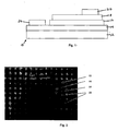
- Fig. 1 shows schematically an embodiment of a capacitor 10 made per the invention.
- a polymer substrate 12 e.g. Mylar TM film
- polythiophene conductor 14 is coated with a one micron layer of polythiophene conductor 14, in turn overlaid with a 100 nanometer tantalum pentoxide film 16 then another one micron layer 18 of the conductor.
- Silver connection pads 20 are applied to the layers 14 and 18.
- Such a capacitor was fabricated. It was tested at five volts and showed a capacitance of about 350 nanofards per sq. cm. of oxide area.
- Fig. 2 is a photograph of such a capacitor with reference numbers indicating the Fig. 1 layers. Fiduciary 1 cm., 1 in. (2.54 cm) markers are shown. The circle of conductive layers 14 is about 2.75 in. (6.98 cm) in diameter.
- the capacitor can be made in 1-30 oxide layers alternating with the conductive layers.
- the substrate film 12 can have a silicone coating and be removed after building the capacitor. Similarly transfer overcoatings can be applied to attach the capacitor to a new substrate.
- the capacitor can be made having more than 30 oxide layers.
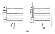
- Figs. 3 a, b show schematically capacitors 10A, 10B with serial and parallel connections of a conductive film (Baytron)-oxide array with three layers of oxide 16, 26, and 36 and four of conductive film 14, 18, 24, and 28, each layer being about one micron.
- a conductive film Boytron
- a thin film capacitor of the invention is generally made by (i) applying a polymeric film comprising a conductive polymer located on a substrate, (ii) applying a pentoxide layer, tantalum pentoxide, or niobium pentoxide, or mixtures thereof to the polymeric conductive layer, and (iii) applying a second conductive polymer located on the pentoxide layer.
- the process steps can be repeated, depending on the number of component layers desired.
- the solution is spread out on the substrate, by any suitable method, such as printing, bar coating, spin coating, or dip coating. After the solution has been applied a drying step is needed to evaporate the carrier solvent(s). In some cases it is advantageous to add some additional solvents and/or binders to the Baytron P solution, which in some cases increases the adherence of the film to the substrate.
- the monomer and oxidant solution are mixed into one solution.
- the solution needs to be spread out on the substrate, which can be accomplished by any known wet method (such as printing, bar coating, spin coating, dip coating). After the solution has been applied a drying step is needed to evaporate the carrier solvent(s). The resulting polymer film is then washed to remove any salts that are formed during the polymerization.
- the methods of establishing the ultra-thin but dense and highly dielectric oxide film include but are not limited to:
Abstract
Description
- The present invention relates to stacks of thin films used as capacitors.
- It is well known in electronic circuits to use capacitors. Printed circuit boards (PCBs) have a limitation of using roll form or powder/ electrolytic capacitors suspended over or under the board. It would be desirable to have a flat capacitor that can be attached directly to the board, or be integrated in the board with adequate electrical parameters and stability (see document
EP-A-1 100 295 ). As such, it is an object of the invention to provide such a capacitor. - It has been discovered that this object can be met by a capacitor that includes alternating layers of tantalum pentoxide or niobium pentoxide and an electrically conductive polymer film such as H.C. Starck, Inc.'s Baytron® line of polythiophene-based polymers. Advantageously, many types of thin conductive polymer films can be used.
- The invention relates to a thin film capacitor that includes (a) a substrate, (b) a first polymeric film made of an electrically conductive polymer located on the substrate, (c) a pentoxide layer selected from the group consisting of tantalum pentoxide, or niobium pentoxide, and mixtures thereof, located on a surface of the first polymeric film, (d) a second polymeric film made of a conductive polymer located on a surface of the pentoxide layer.
- These and other features, aspects, and advantages of the present invention will become better understood with reference to the following description and appended claims, where:
-
Fig. 1 shows schematically an embodiment of a capacitor made in accordance with the invention; -
Fig. 2 is a photograph of such a capacitor; -
Figs. 3a, and 3b show schematically serial and parallel connections of a conductive poly(3,4-ethylenedioxythiophene) film (Baytron) oxide array with 3 layers. - The invention relates to a thin film capacitor comprising (a) a substrate, (b) a first polymeric film made of a conductive polymer located on the substrate, (c) a pentoxide layer selected from the group consisting of tantalum pentoxide, or niobium pentoxide, and mixtures thereof, and (d) a second polymeric film made of a conductive polymer located on the pentoxide layer.
- The substrate can be any substrate, which when used in accordance with the invention, enables the resulting thin film capacitor to be used in its intended application. Generally, the substrate is a non-conductive substrate and can be selected from materials such as vinyl polymers, olefin polymers or polyester polymers. The thickness of the substrate is generally at least about about 0.01 mm. The thickness of the substrate can vary widely, depending on the application. In one embodiment, the thickness ranges from about 0.01 to about 1mm.
- A polymeric film can include any electrically conductive polymer, which when used in accordance with the invention, enables the resulting thin film capacitor to be used in its intended use. Examples of suitable conductive polymers include polyaniline-based polymers, polypyrrole-based polymers, polyethyleneoxide-based polymers, polythiophene-based polymers, and mixtures or copolymers thereof. These polymers are well known in the art.
- Particularly advantageous conductive polymers are included in the BAYTRON® line of conductive polymers, available from H.C. Starck, Inc, preferably conductive poly(3,4ethylene dioxythiophene), as described in
US. Patent 5,035,926 , see documentWO-A-00 19 469 - One such polythiophene preferred polymer, "Baytron P" is an aqueous polymer dispersion that exhibits good adhesion. If necessary, adhesion can be improved by addition of binders. Such an aqueous dispersion is easily applied to plastic and glass surfaces, e.g., by printing or spraying, and is water-based and thus environmentally friendly.
- The conductive polymer is generally combined with suitable binders for coating. Examples of suitable binders include but are not limited to polyvinyl acetate, polycarbonate, polyvinyl butyrate, polyacrylates, polymethacrylates, polystyrene, polyacrylonitrile, polyvinyl chloride, polybutadiene, polyisoprene, polyethers, polyesters, silicones, pyrrole/acecrylate, vinyl acetate/acrylate, ethylene/vinyl acetate copolymers, poly vinyl alcohols.
- The thickness of a conductive polymeric film is generally at least about 50 nanometers and preferably ranges from about 100 nanometers to about 10 micrometers, depending on the application.
- In one embodiment, the invention relates to a thin film capacitor including (a) a substrate, (b) a first polymeric conductive layer located on a surface of the substrate and (c) a plurality of alternating pentoxide layer/polymeric conductive layers extending from the first polymeric layer, wherein the total number of pentoxide layers is n and the total number of polymeric conductive layers is n+1, in which n preferably ranges from 1 to 30. In another embodiment, there can be 2 to 20 layers of each of the components (generally more conductive film layer than oxide layers). Serial or parallel connections can be made to each of the virtual capacitors in such a stack. Preferably, the whole stack of films is on a non-conductive substrate such as a vinyl, olefin or polyester film.
- In one embodiment, each of the conductive films is about one micron thick and applied by printing, spraying or other wet methods from liquid or solution precursors. In another embodiment, each of the Ta, Nb-oxide films is about one micron thick and applied by reaction physical vapor deposition (PVD) or chemical methods from liquid or vapor precursors. Alternatively Ta or Nb can be applied and oxidized in situ.
- The capacitors so made have an advantage over known Ta2O5/Cu/Ta2O5/Cu.... stacks in that the present stacks will be less susceptible to deterioration under influence of environmental humidity. Also a short stack (2-4 layers each of oxide and polymer) can be transparent.
- Referring to the figures,
Fig. 1 shows schematically an embodiment of acapacitor 10 made per the invention. A polymer substrate 12 (e.g. Mylar™ film) is coated with a one micron layer ofpolythiophene conductor 14, in turn overlaid with a 100 nanometertantalum pentoxide film 16 then another onemicron layer 18 of the conductor.Silver connection pads 20 are applied to thelayers -
Fig. 2 is a photograph of such a capacitor with reference numbers indicating theFig. 1 layers. Fiduciary 1 cm., 1 in. (2.54 cm) markers are shown. The circle ofconductive layers 14 is about 2.75 in. (6.98 cm) in diameter. - In one embodiment, the capacitor can be made in 1-30 oxide layers alternating with the conductive layers. If desired the
substrate film 12 can have a silicone coating and be removed after building the capacitor. Similarly transfer overcoatings can be applied to attach the capacitor to a new substrate. In other embodiments, the capacitor can be made having more than 30 oxide layers. -
Figs. 3 a, b show schematicallycapacitors oxide conductive film - A thin film capacitor of the invention is generally made by (i) applying a polymeric film comprising a conductive polymer located on a substrate, (ii) applying a pentoxide layer, tantalum pentoxide, or niobium pentoxide, or mixtures thereof to the polymeric conductive layer, and (iii) applying a second conductive polymer located on the pentoxide layer. The process steps can be repeated, depending on the number of component layers desired.
- When polythiophene-based polymers in aqueous solutions are used, the solution is spread out on the substrate, by any suitable method, such as printing, bar coating, spin coating, or dip coating. After the solution has been applied a drying step is needed to evaporate the carrier solvent(s). In some cases it is advantageous to add some additional solvents and/or binders to the Baytron P solution, which in some cases increases the adherence of the film to the substrate.
- When it is desirable to perform in-situ polymerization and make the polymeric conductive thin film onto the layer, the monomer and oxidant solution are mixed into one solution. The solution needs to be spread out on the substrate, which can be accomplished by any known wet method (such as printing, bar coating, spin coating, dip coating). After the solution has been applied a drying step is needed to evaporate the carrier solvent(s). The resulting polymer film is then washed to remove any salts that are formed during the polymerization.
- The methods of establishing the ultra-thin but dense and highly dielectric oxide film include but are not limited to:
- (a) physical vapor deposition (PVD) methods of, e.g., reactive sputtering or laser or EB scan heating of Ta, Nb targets to form oxide as deposited;
- (b) sputtering an oxide target to transfer oxide to a film substrate (or to top a previously laid conductive layer);
- (c) coating with a Ta, Nb film by any known method and anodizing it (by electrolytic or chemical anodization). In such case the film would be partly oxidized and the non-oxidized part becomes a part of the adjacent conductive layer.
- Although the present invention has been described in detail with reference to certain preferred versions thereof, other variations are possible. The scope of the invention is defined by the appended claims.
Claims (18)
- A thin film capacitor comprising:(a) a substrate,(b) a first polymeric film made of an electrically conductive polymer located on the substrate,(c) a pentoxide layer selected from the group consisting of tantalum pentoxide, or niobium pentoxide, and mixtures thereof, and located on a surface of the first polymeric film,(d) a second polymeric film made of an electrically conductive polymer located on a surface of the pentoxide layer.
- The thin film capactior of Claim 1, wherein the substrate is selected from the group consisting of vinyl polymers, olefin polymers, polyesters, and mixtures thereof.
- The thin film capacitor of Claim 1, wherein the first polymeric film and the second polymeric film is selected from the group consisting of polyanilin polymers, ligno-sulfonic acid polymers, poly pyrrol polymers, thiophene-based polymers, and mixtures thereof.
- The thin film capacitor of Claim 1, wherein the first polymeric film has a thickness ranging from about 100 nanometers to about 10 micrometers.
- The thin film capacitor of Claim 1, wherein the pentoxide layer has a thickness ranging from about 10 to about 100 nanometers.
- The thin film capacitor of claim 1 wherein the substrate has a thickness that is at least about 0.01 mm.
- The thin film capacitor of Claim 1, wherein the first polymeric film or the second polymeric film is selected from the group consisting of polythiophene-based polymers, polyaniline-based polymers, polypyrrole-based polymers, polyethyleneoxide-based polymers, and mixtures or copolymers thereof.
- A thin film capacitor comprising: (a) a substrate, (b) a first polymeric conductive layer located on a surface of the substrate and (c) a plurality of alternating pentoxide layer/polymeric conductive layers extending from the first polymeric layer, wherein the total number of pentoxide layers is n and the total number of polymeric conductive layers is n+1.
- The thin film capacitor of Claim 8, wherein n ranges from 1 to 30.
- The thin film capacitor of Claim 8, wherein the capacitor has a series connection.
- The thin film capacitor of Claim 8, wherein the capacitor has a parallel connection.
- The thin film capacitor of Claim 8, wherein the substrate is a non-conductive substrate selected from the group consisting of vinyl polymers, olefin polymers, polyester polymers and mixtures thereof.
- The thin film capacitor of Claim 8, wherein the substrate is selected from the group consisting of vinyl polymers, olefin polymers, polyesters, and mixtures thereof.
- The thin film capacitor of Claim 8, wherein at least one polymeric film is selected from the group consisting of polyaniline-based polymers, polypyrrole-based polymers, polyethyleneoxide-based polymers, polythiophene-based polymers, and mixtures or copolymers thereof.
- A method for making a thin film capacitor of claim 1 comprising:(a) applying a first electrically conductive polymer located on a substrate,(b) applying a pentoxide layer, tantalum pentoxide, or niobium pentoxide, or mixtures thereof to the polymeric conductive layer, and(c) applying a second electrically conductive polymer located on the pentoxide layer, and thereby forming a thin film capacitor.
- The method of Claim 15, wherein the thin film capacitor formed comprises:(a) a substrate,(b) a first polymeric film comprising an electrically conductive polymer located on the substrate,(c) a pentoxide layer selected from the group consisting of tantalum pentoxide, or niobium pentoxide, and mixtures thereof, located on a surface of the first polymeric film,(d) a second polymeric film comprising an electrically conductive polymer located on a surface of the pentoxide layer.
- The method of Claim 15, wherein the thin film capacitor comprises (a) a substrate, (b) a first polymeric conductive layer located on a surface of the substrate and (c) a plurality of alternating pentoxide layer/polymeric electrically conductive layers extending from the first polymeric layer, wherein the total number of pentoxide layers is n and the total number of polymeric conductive layers is n+1.
- The method of Claim 15, wherein the wherein the first polymeric film and the second polymeric film is selected from the group consisting of polyaniline-based polymers, polypyrrole-based polymers, polyethyleneoxide-based polymers, polythiophene-based polymers, and mixtures or copolymers thereof.
Applications Claiming Priority (3)
| Application Number | Priority Date | Filing Date | Title |
|---|---|---|---|
| US33771901P | 2001-11-03 | 2001-11-03 | |
| US337719P | 2001-11-03 | ||
| PCT/US2002/035261 WO2003041096A1 (en) | 2001-11-03 | 2002-11-01 | Thin film capacitor using conductive polymers |
Publications (2)
| Publication Number | Publication Date |
|---|---|
| EP1444710A1 EP1444710A1 (en) | 2004-08-11 |
| EP1444710B1 true EP1444710B1 (en) | 2009-10-21 |
Family
ID=23321725
Family Applications (1)
| Application Number | Title | Priority Date | Filing Date |
|---|---|---|---|
| EP02778712A Expired - Lifetime EP1444710B1 (en) | 2001-11-03 | 2002-11-01 | Thin film capacitor using conductive polymers |
Country Status (17)
| Country | Link |
|---|---|
| US (2) | US6731495B2 (en) |
| EP (1) | EP1444710B1 (en) |
| JP (1) | JP4328909B2 (en) |
| KR (1) | KR100974771B1 (en) |
| CN (1) | CN100449661C (en) |
| AT (1) | ATE446583T1 (en) |
| BR (1) | BR0213858A (en) |
| CA (1) | CA2465269A1 (en) |
| DE (1) | DE60234114D1 (en) |
| IL (2) | IL161634A0 (en) |
| MX (1) | MXPA04004147A (en) |
| NZ (1) | NZ532671A (en) |
| PL (1) | PL369208A1 (en) |
| RU (1) | RU2318263C2 (en) |
| UA (1) | UA77459C2 (en) |
| WO (1) | WO2003041096A1 (en) |
| ZA (1) | ZA200403225B (en) |
Families Citing this family (39)
| Publication number | Priority date | Publication date | Assignee | Title |
|---|---|---|---|---|
| UA77459C2 (en) | 2001-11-03 | 2006-12-15 | Thin-film capacitor and a method for producing the capacitor | |
| US7079377B2 (en) * | 2002-09-30 | 2006-07-18 | Joachim Hossick Schott | Capacitor and method for producing a capacitor |
| US7256982B2 (en) * | 2003-05-30 | 2007-08-14 | Philip Michael Lessner | Electrolytic capacitor |
| GB0323733D0 (en) * | 2003-10-10 | 2003-11-12 | Univ Heriot Watt | Conductive polymer |
| ES2329898T3 (en) * | 2003-10-17 | 2009-12-02 | H.C. Starck Gmbh | ELECTROLYTIC CONDENSERS WITH EXTERNAL POLYMER COAT. |
| JP2005268672A (en) * | 2004-03-22 | 2005-09-29 | Mitsubishi Electric Corp | Substrate |
| JP2007194592A (en) * | 2005-12-20 | 2007-08-02 | Tdk Corp | Dielectric element, and method of manufacturing same |
| US7612727B2 (en) * | 2005-12-29 | 2009-11-03 | Exatec, Llc | Antenna for plastic window panel |
| WO2007123752A2 (en) * | 2006-03-31 | 2007-11-01 | Aculon, Inc. | Solid electrolytic capacitors |
| JP2008181091A (en) * | 2006-12-26 | 2008-08-07 | Nitto Denko Corp | Optical laminate and liquid crystal panel using the same |
| US8461681B2 (en) | 2007-04-27 | 2013-06-11 | Medtronic, Inc. | Layered structure for corrosion resistant interconnect contacts |
| US8141556B2 (en) * | 2007-04-27 | 2012-03-27 | Medtronic, Inc. | Metallization with tailorable coefficient of thermal expansion |
| EP2198396B1 (en) * | 2007-10-10 | 2019-09-25 | Thin Film Electronics ASA | High reliability surveillance and/or identification tag/devices and methods of making and using the same |
| US8357858B2 (en) * | 2008-11-12 | 2013-01-22 | Simon Fraser University | Electrically conductive, thermosetting elastomeric material and uses therefor |
| CN103000379B (en) * | 2012-10-18 | 2016-04-20 | 中国科学院化学研究所 | A kind of method improving all-solid-state electrical energy storage device charge efficiency |
| EP2972700B1 (en) | 2013-03-15 | 2019-05-08 | Gottlieb, Stacey | Fingernail system for use with capacitive touchscreens |
| RU2540934C1 (en) * | 2013-10-15 | 2015-02-10 | Открытое акционерное общество "Обнинское научно-производственное предприятие "Технология" | Sensor for control of filler impregnation with polymeric binder |
| US10340082B2 (en) | 2015-05-12 | 2019-07-02 | Capacitor Sciences Incorporated | Capacitor and method of production thereof |
| WO2015175558A2 (en) * | 2014-05-12 | 2015-11-19 | Capacitor Sciences Incorporated | Energy storage device and method of production thereof |
| US10347423B2 (en) | 2014-05-12 | 2019-07-09 | Capacitor Sciences Incorporated | Solid multilayer structure as semiproduct for meta-capacitor |
| US10319523B2 (en) | 2014-05-12 | 2019-06-11 | Capacitor Sciences Incorporated | Yanli dielectric materials and capacitor thereof |
| US20170301477A1 (en) | 2016-04-04 | 2017-10-19 | Capacitor Sciences Incorporated | Electro-polarizable compound and capacitor |
| WO2016073522A1 (en) * | 2014-11-04 | 2016-05-12 | Capacitor Sciences Incorporated | Energy storage devices and methods of production thereof |
| US10037850B2 (en) * | 2014-12-18 | 2018-07-31 | 3M Innovative Properties Company | Multilayer film capacitor |
| US9932358B2 (en) | 2015-05-21 | 2018-04-03 | Capacitor Science Incorporated | Energy storage molecular material, crystal dielectric layer and capacitor |
| US9941051B2 (en) | 2015-06-26 | 2018-04-10 | Capactor Sciences Incorporated | Coiled capacitor |
| US10026553B2 (en) | 2015-10-21 | 2018-07-17 | Capacitor Sciences Incorporated | Organic compound, crystal dielectric layer and capacitor |
| US10636575B2 (en) | 2016-02-12 | 2020-04-28 | Capacitor Sciences Incorporated | Furuta and para-Furuta polymer formulations and capacitors |
| US10305295B2 (en) | 2016-02-12 | 2019-05-28 | Capacitor Sciences Incorporated | Energy storage cell, capacitive energy storage module, and capacitive energy storage system |
| US10566138B2 (en) | 2016-04-04 | 2020-02-18 | Capacitor Sciences Incorporated | Hein electro-polarizable compound and capacitor thereof |
| US9978517B2 (en) | 2016-04-04 | 2018-05-22 | Capacitor Sciences Incorporated | Electro-polarizable compound and capacitor |
| US10153087B2 (en) | 2016-04-04 | 2018-12-11 | Capacitor Sciences Incorporated | Electro-polarizable compound and capacitor |
| US10395841B2 (en) | 2016-12-02 | 2019-08-27 | Capacitor Sciences Incorporated | Multilayered electrode and film energy storage device |
| US10163575B1 (en) | 2017-11-07 | 2018-12-25 | Capacitor Sciences Incorporated | Non-linear capacitor and energy storage device comprising thereof |
| US11049664B2 (en) | 2018-04-13 | 2021-06-29 | Avx Corporation | Solid electrolytic capacitor containing a vapor-deposited barrier film |
| WO2019199485A1 (en) | 2018-04-13 | 2019-10-17 | Avx Corporation | Solid electrolytic capacitor containing an adhesive film |
| KR102412561B1 (en) | 2018-04-13 | 2022-06-23 | 교세라 에이브이엑스 컴포넌츠 코포레이션 | Solid Electrolytic Capacitors Containing Sequentially Deposited Internally Conductive Polymer Films |
| US11183339B2 (en) | 2018-11-29 | 2021-11-23 | Avx Corporation | Solid electrolytic capacitor containing a sequential vapor-deposited dielectric film |
| CN110845728B (en) * | 2019-11-07 | 2020-12-29 | 江南大学 | Preparation method and application of conductive polymer/niobium pentoxide heterojunction |
Family Cites Families (12)
| Publication number | Priority date | Publication date | Assignee | Title |
|---|---|---|---|---|
| JPS4870855A (en) * | 1971-12-29 | 1973-09-26 | ||
| US5126921A (en) * | 1990-07-06 | 1992-06-30 | Akira Fujishima | Electronic component and a method for manufacturing the same |
| JPH0547588A (en) | 1991-08-21 | 1993-02-26 | Rubikon Denshi Kk | Thin film capacitor and manufacture thereof |
| JPH05114532A (en) | 1991-10-23 | 1993-05-07 | Yoshiyasu Sasa | Multilayered capacitor |
| JPH09283389A (en) * | 1996-04-10 | 1997-10-31 | Matsushita Electric Ind Co Ltd | Capacitor and its manufacture |
| US5978207A (en) * | 1996-10-30 | 1999-11-02 | The Research Foundation Of The State University Of New York | Thin film capacitor |
| CA2289239C (en) | 1998-11-23 | 2010-07-20 | Micro Coating Technologies | Formation of thin film capacitors |
| EP1014399B1 (en) * | 1998-12-22 | 2006-05-17 | Matsushita Electric Industrial Co., Ltd. | Flexible thin film capacitor and method for producing the same |
| EP1170797A3 (en) * | 2000-07-04 | 2005-05-25 | Alps Electric Co., Ltd. | Thin-film capacitor element and electronic circuit board on which thin-film capacitor element is formed |
| JP3624822B2 (en) | 2000-11-22 | 2005-03-02 | 株式会社日立製作所 | Semiconductor device and manufacturing method thereof |
| JP2002252143A (en) * | 2000-12-21 | 2002-09-06 | Alps Electric Co Ltd | Temperature compensating thin-film capacitor and electronic apparatus |
| UA77459C2 (en) | 2001-11-03 | 2006-12-15 | Thin-film capacitor and a method for producing the capacitor |
-
2002
- 2002-01-11 UA UA20040604241A patent/UA77459C2/en unknown
- 2002-11-01 BR BR0213858-1A patent/BR0213858A/en not_active IP Right Cessation
- 2002-11-01 PL PL02369208A patent/PL369208A1/en unknown
- 2002-11-01 AT AT02778712T patent/ATE446583T1/en not_active IP Right Cessation
- 2002-11-01 MX MXPA04004147A patent/MXPA04004147A/en active IP Right Grant
- 2002-11-01 US US10/285,748 patent/US6731495B2/en not_active Expired - Fee Related
- 2002-11-01 RU RU2004116913/09A patent/RU2318263C2/en not_active IP Right Cessation
- 2002-11-01 IL IL16163402A patent/IL161634A0/en unknown
- 2002-11-01 CA CA002465269A patent/CA2465269A1/en not_active Abandoned
- 2002-11-01 WO PCT/US2002/035261 patent/WO2003041096A1/en active Application Filing
- 2002-11-01 JP JP2003543043A patent/JP4328909B2/en not_active Expired - Fee Related
- 2002-11-01 CN CNB028217896A patent/CN100449661C/en not_active Expired - Fee Related
- 2002-11-01 KR KR1020047006497A patent/KR100974771B1/en not_active IP Right Cessation
- 2002-11-01 DE DE60234114T patent/DE60234114D1/en not_active Expired - Lifetime
- 2002-11-01 NZ NZ532671A patent/NZ532671A/en unknown
- 2002-11-01 EP EP02778712A patent/EP1444710B1/en not_active Expired - Lifetime
-
2004
- 2004-03-16 US US10/801,324 patent/US6912113B2/en not_active Expired - Fee Related
- 2004-04-26 IL IL161634A patent/IL161634A/en not_active IP Right Cessation
- 2004-04-29 ZA ZA200403225A patent/ZA200403225B/en unknown
Also Published As
| Publication number | Publication date |
|---|---|
| PL369208A1 (en) | 2005-04-18 |
| BR0213858A (en) | 2004-08-31 |
| IL161634A0 (en) | 2004-09-27 |
| UA77459C2 (en) | 2006-12-15 |
| WO2003041096A1 (en) | 2003-05-15 |
| ZA200403225B (en) | 2005-04-29 |
| JP4328909B2 (en) | 2009-09-09 |
| US6731495B2 (en) | 2004-05-04 |
| CN1578993A (en) | 2005-02-09 |
| CN100449661C (en) | 2009-01-07 |
| KR20040064697A (en) | 2004-07-19 |
| MXPA04004147A (en) | 2004-09-06 |
| JP2005509283A (en) | 2005-04-07 |
| US20040173873A1 (en) | 2004-09-09 |
| ATE446583T1 (en) | 2009-11-15 |
| NZ532671A (en) | 2006-02-24 |
| DE60234114D1 (en) | 2009-12-03 |
| US6912113B2 (en) | 2005-06-28 |
| RU2318263C2 (en) | 2008-02-27 |
| EP1444710A1 (en) | 2004-08-11 |
| IL161634A (en) | 2010-11-30 |
| RU2004116913A (en) | 2005-10-27 |
| KR100974771B1 (en) | 2010-08-06 |
| US20030103319A1 (en) | 2003-06-05 |
| CA2465269A1 (en) | 2003-05-15 |
Similar Documents
| Publication | Publication Date | Title |
|---|---|---|
| EP1444710B1 (en) | Thin film capacitor using conductive polymers | |
| CN101023138B (en) | Conductive composition and process for production thereof, antistatic coating material, antistatic membrane, antistatic film, optical filter, optical information recording media, and condenser and pro | |
| RU2327708C2 (en) | Method of obtaining water dispersion containing complex of poly(3,4-dialkoxythiophen) and polyanion, coating composition, substrate with conducting transparent film obtained using above given method | |
| CN103160121B (en) | Electroconductive polymer composition, electroconductive polymer material, electroconductive substrate, electrode and solid electrolytic capacitor | |
| EP1003179B1 (en) | A method for preparing a conductive polythiophene layer at low temperature | |
| US6340496B1 (en) | Method for patterning a layer of conductive polymers | |
| JP4491098B2 (en) | Method for forming a conductive polythiophene layer at low temperature | |
| WO2016143715A1 (en) | Transparent conductor and method for producing transparent conductor | |
| EP1402319B1 (en) | Material having a conductive pattern; and a material and method for making a conductive pattern | |
| TW200938601A (en) | Process for the preparation of coatings exhibiting increased conductivity based on polythiophene and its derivatives | |
| CN103131137A (en) | Electroconductive polymer composition, electroconductive polymer material, electroconductive substrate, electrode and solid electrolytic capacitor | |
| AU2002340360A1 (en) | Thin film capacitor using conductive polymers | |
| NZ541932A (en) | Thin film capacitor using conductive polymers | |
| US5888582A (en) | Polyaniline solutions with bicyclic terpene solvent | |
| JP5600019B2 (en) | Metal laminate | |
| JPS62140410A (en) | Metallized plastic film capacitor | |
| JPH02290008A (en) | Metallized plastic film capacitor | |
| JPS613742A (en) | Conductive high-molecular sheet and manufacture thereof | |
| EP1402543A1 (en) | Material and method for making an electroconductive pattern | |
| JPS62134918A (en) | Organic laminated film capacitor |
Legal Events
| Date | Code | Title | Description |
|---|---|---|---|
| PUAI | Public reference made under article 153(3) epc to a published international application that has entered the european phase |
Free format text: ORIGINAL CODE: 0009012 |
|
| 17P | Request for examination filed |
Effective date: 20040603 |
|
| AK | Designated contracting states |
Kind code of ref document: A1 Designated state(s): AT BE BG CH CY CZ DE DK EE ES FI FR GB GR IE IT LI LU MC NL PT SE SK TR |
|
| AX | Request for extension of the european patent |
Extension state: AL LT LV MK RO SI |
|
| RIN1 | Information on inventor provided before grant (corrected) |
Inventor name: KUMAR, PRABHAT Inventor name: UHLENHUT, HENNING |
|
| GRAP | Despatch of communication of intention to grant a patent |
Free format text: ORIGINAL CODE: EPIDOSNIGR1 |
|
| DAX | Request for extension of the european patent (deleted) | ||
| RAX | Requested extension states of the european patent have changed |
Extension state: RO Payment date: 20040603 |
|
| GRAS | Grant fee paid |
Free format text: ORIGINAL CODE: EPIDOSNIGR3 |
|
| GRAA | (expected) grant |
Free format text: ORIGINAL CODE: 0009210 |
|
| RAP1 | Party data changed (applicant data changed or rights of an application transferred) |
Owner name: H.C. STARCK GMBH |
|
| AK | Designated contracting states |
Kind code of ref document: B1 Designated state(s): AT BE BG CH CY CZ DE DK EE ES FI FR GB GR IE IT LI LU MC NL PT SE SK TR |
|
| AX | Request for extension of the european patent |
Extension state: RO |
|
| REG | Reference to a national code |
Ref country code: GB Ref legal event code: FG4D |
|
| REG | Reference to a national code |
Ref country code: CH Ref legal event code: EP |
|
| RAP2 | Party data changed (patent owner data changed or rights of a patent transferred) |
Owner name: H.C. STARCK CLEVIOS GMBH |
|
| REG | Reference to a national code |
Ref country code: IE Ref legal event code: FG4D |
|
| REF | Corresponds to: |
Ref document number: 60234114 Country of ref document: DE Date of ref document: 20091203 Kind code of ref document: P |
|
| NLT2 | Nl: modifications (of names), taken from the european patent patent bulletin |
Owner name: H.C. STARCK CLEVIOS GMBH Effective date: 20091104 |
|
| NLV1 | Nl: lapsed or annulled due to failure to fulfill the requirements of art. 29p and 29m of the patents act | ||
| PG25 | Lapsed in a contracting state [announced via postgrant information from national office to epo] |
Ref country code: FI Free format text: LAPSE BECAUSE OF FAILURE TO SUBMIT A TRANSLATION OF THE DESCRIPTION OR TO PAY THE FEE WITHIN THE PRESCRIBED TIME-LIMIT Effective date: 20091021 Ref country code: PT Free format text: LAPSE BECAUSE OF FAILURE TO SUBMIT A TRANSLATION OF THE DESCRIPTION OR TO PAY THE FEE WITHIN THE PRESCRIBED TIME-LIMIT Effective date: 20100222 Ref country code: SE Free format text: LAPSE BECAUSE OF FAILURE TO SUBMIT A TRANSLATION OF THE DESCRIPTION OR TO PAY THE FEE WITHIN THE PRESCRIBED TIME-LIMIT Effective date: 20091021 Ref country code: ES Free format text: LAPSE BECAUSE OF FAILURE TO SUBMIT A TRANSLATION OF THE DESCRIPTION OR TO PAY THE FEE WITHIN THE PRESCRIBED TIME-LIMIT Effective date: 20100201 |
|
| PG25 | Lapsed in a contracting state [announced via postgrant information from national office to epo] |
Ref country code: AT Free format text: LAPSE BECAUSE OF FAILURE TO SUBMIT A TRANSLATION OF THE DESCRIPTION OR TO PAY THE FEE WITHIN THE PRESCRIBED TIME-LIMIT Effective date: 20091021 Ref country code: MC Free format text: LAPSE BECAUSE OF NON-PAYMENT OF DUE FEES Effective date: 20091130 Ref country code: BE Free format text: LAPSE BECAUSE OF FAILURE TO SUBMIT A TRANSLATION OF THE DESCRIPTION OR TO PAY THE FEE WITHIN THE PRESCRIBED TIME-LIMIT Effective date: 20091021 |
|
| REG | Reference to a national code |
Ref country code: CH Ref legal event code: PL |
|
| PG25 | Lapsed in a contracting state [announced via postgrant information from national office to epo] |
Ref country code: EE Free format text: LAPSE BECAUSE OF FAILURE TO SUBMIT A TRANSLATION OF THE DESCRIPTION OR TO PAY THE FEE WITHIN THE PRESCRIBED TIME-LIMIT Effective date: 20091021 Ref country code: BG Free format text: LAPSE BECAUSE OF FAILURE TO SUBMIT A TRANSLATION OF THE DESCRIPTION OR TO PAY THE FEE WITHIN THE PRESCRIBED TIME-LIMIT Effective date: 20100121 Ref country code: DK Free format text: LAPSE BECAUSE OF FAILURE TO SUBMIT A TRANSLATION OF THE DESCRIPTION OR TO PAY THE FEE WITHIN THE PRESCRIBED TIME-LIMIT Effective date: 20091021 |
|
| PLBE | No opposition filed within time limit |
Free format text: ORIGINAL CODE: 0009261 |
|
| STAA | Information on the status of an ep patent application or granted ep patent |
Free format text: STATUS: NO OPPOSITION FILED WITHIN TIME LIMIT |
|
| PG25 | Lapsed in a contracting state [announced via postgrant information from national office to epo] |
Ref country code: SK Free format text: LAPSE BECAUSE OF FAILURE TO SUBMIT A TRANSLATION OF THE DESCRIPTION OR TO PAY THE FEE WITHIN THE PRESCRIBED TIME-LIMIT Effective date: 20091021 Ref country code: CZ Free format text: LAPSE BECAUSE OF FAILURE TO SUBMIT A TRANSLATION OF THE DESCRIPTION OR TO PAY THE FEE WITHIN THE PRESCRIBED TIME-LIMIT Effective date: 20091021 |
|
| 26N | No opposition filed |
Effective date: 20100722 |
|
| PG25 | Lapsed in a contracting state [announced via postgrant information from national office to epo] |
Ref country code: LI Free format text: LAPSE BECAUSE OF NON-PAYMENT OF DUE FEES Effective date: 20091130 Ref country code: CH Free format text: LAPSE BECAUSE OF NON-PAYMENT OF DUE FEES Effective date: 20091130 Ref country code: IE Free format text: LAPSE BECAUSE OF NON-PAYMENT OF DUE FEES Effective date: 20091101 Ref country code: GR Free format text: LAPSE BECAUSE OF FAILURE TO SUBMIT A TRANSLATION OF THE DESCRIPTION OR TO PAY THE FEE WITHIN THE PRESCRIBED TIME-LIMIT Effective date: 20100122 |
|
| PGFP | Annual fee paid to national office [announced via postgrant information from national office to epo] |
Ref country code: FR Payment date: 20101123 Year of fee payment: 9 |
|
| PG25 | Lapsed in a contracting state [announced via postgrant information from national office to epo] |
Ref country code: IT Free format text: LAPSE BECAUSE OF FAILURE TO SUBMIT A TRANSLATION OF THE DESCRIPTION OR TO PAY THE FEE WITHIN THE PRESCRIBED TIME-LIMIT Effective date: 20091021 |
|
| PGFP | Annual fee paid to national office [announced via postgrant information from national office to epo] |
Ref country code: GB Payment date: 20101027 Year of fee payment: 9 |
|
| PG25 | Lapsed in a contracting state [announced via postgrant information from national office to epo] |
Ref country code: LU Free format text: LAPSE BECAUSE OF NON-PAYMENT OF DUE FEES Effective date: 20091101 |
|
| PG25 | Lapsed in a contracting state [announced via postgrant information from national office to epo] |
Ref country code: TR Free format text: LAPSE BECAUSE OF FAILURE TO SUBMIT A TRANSLATION OF THE DESCRIPTION OR TO PAY THE FEE WITHIN THE PRESCRIBED TIME-LIMIT Effective date: 20091021 |
|
| PG25 | Lapsed in a contracting state [announced via postgrant information from national office to epo] |
Ref country code: CY Free format text: LAPSE BECAUSE OF FAILURE TO SUBMIT A TRANSLATION OF THE DESCRIPTION OR TO PAY THE FEE WITHIN THE PRESCRIBED TIME-LIMIT Effective date: 20091021 |
|
| REG | Reference to a national code |
Ref country code: GB Ref legal event code: 732E Free format text: REGISTERED BETWEEN 20111215 AND 20111221 |
|
| GBPC | Gb: european patent ceased through non-payment of renewal fee |
Effective date: 20111101 |
|
| REG | Reference to a national code |
Ref country code: FR Ref legal event code: ST Effective date: 20120731 |
|
| PG25 | Lapsed in a contracting state [announced via postgrant information from national office to epo] |
Ref country code: NL Free format text: LAPSE BECAUSE OF FAILURE TO SUBMIT A TRANSLATION OF THE DESCRIPTION OR TO PAY THE FEE WITHIN THE PRESCRIBED TIME-LIMIT Effective date: 20091021 |
|
| PG25 | Lapsed in a contracting state [announced via postgrant information from national office to epo] |
Ref country code: GB Free format text: LAPSE BECAUSE OF NON-PAYMENT OF DUE FEES Effective date: 20111101 |
|
| PG25 | Lapsed in a contracting state [announced via postgrant information from national office to epo] |
Ref country code: FR Free format text: LAPSE BECAUSE OF NON-PAYMENT OF DUE FEES Effective date: 20111130 |
|
| REG | Reference to a national code |
Ref country code: DE Ref legal event code: R081 Ref document number: 60234114 Country of ref document: DE Owner name: HERAEUS PRECIOUS METALS GMBH & CO. KG, DE Free format text: FORMER OWNER: H.C. STARCK CLEVIOS GMBH, 38642 GOSLAR, DE Effective date: 20131106 |
|
| PGFP | Annual fee paid to national office [announced via postgrant information from national office to epo] |
Ref country code: DE Payment date: 20131121 Year of fee payment: 12 |
|
| REG | Reference to a national code |
Ref country code: DE Ref legal event code: R119 Ref document number: 60234114 Country of ref document: DE |
|
| PG25 | Lapsed in a contracting state [announced via postgrant information from national office to epo] |
Ref country code: DE Free format text: LAPSE BECAUSE OF NON-PAYMENT OF DUE FEES Effective date: 20150602 |