EP1445786A2 - Gas discharge panel and its production method - Google Patents
Gas discharge panel and its production method Download PDFInfo
- Publication number
- EP1445786A2 EP1445786A2 EP04250402A EP04250402A EP1445786A2 EP 1445786 A2 EP1445786 A2 EP 1445786A2 EP 04250402 A EP04250402 A EP 04250402A EP 04250402 A EP04250402 A EP 04250402A EP 1445786 A2 EP1445786 A2 EP 1445786A2
- Authority
- EP
- European Patent Office
- Prior art keywords
- dielectric layer
- atom
- gas discharge
- discharge panel
- pdp
- Prior art date
- Legal status (The legal status is an assumption and is not a legal conclusion. Google has not performed a legal analysis and makes no representation as to the accuracy of the status listed.)
- Granted
Links
- 0 O=N*1C2(C34)C5(CCC/C(/C6)=C/C7)C3C63C1C4C7C2C5CC3 Chemical compound O=N*1C2(C34)C5(CCC/C(/C6)=C/C7)C3C63C1C4C7C2C5CC3 0.000 description 1
Images


Classifications
-
- H—ELECTRICITY
- H01—ELECTRIC ELEMENTS
- H01J—ELECTRIC DISCHARGE TUBES OR DISCHARGE LAMPS
- H01J11/00—Gas-filled discharge tubes with alternating current induction of the discharge, e.g. alternating current plasma display panels [AC-PDP]; Gas-filled discharge tubes without any main electrode inside the vessel; Gas-filled discharge tubes with at least one main electrode outside the vessel
- H01J11/20—Constructional details
- H01J11/34—Vessels, containers or parts thereof, e.g. substrates
- H01J11/38—Dielectric or insulating layers
-
- E—FIXED CONSTRUCTIONS
- E02—HYDRAULIC ENGINEERING; FOUNDATIONS; SOIL SHIFTING
- E02D—FOUNDATIONS; EXCAVATIONS; EMBANKMENTS; UNDERGROUND OR UNDERWATER STRUCTURES
- E02D29/00—Independent underground or underwater structures; Retaining walls
- E02D29/02—Retaining or protecting walls
- E02D29/0258—Retaining or protecting walls characterised by constructional features
- E02D29/0291—Retaining or protecting walls characterised by constructional features made up of filled, bag-like elements
-
- C—CHEMISTRY; METALLURGY
- C23—COATING METALLIC MATERIAL; COATING MATERIAL WITH METALLIC MATERIAL; CHEMICAL SURFACE TREATMENT; DIFFUSION TREATMENT OF METALLIC MATERIAL; COATING BY VACUUM EVAPORATION, BY SPUTTERING, BY ION IMPLANTATION OR BY CHEMICAL VAPOUR DEPOSITION, IN GENERAL; INHIBITING CORROSION OF METALLIC MATERIAL OR INCRUSTATION IN GENERAL
- C23C—COATING METALLIC MATERIAL; COATING MATERIAL WITH METALLIC MATERIAL; SURFACE TREATMENT OF METALLIC MATERIAL BY DIFFUSION INTO THE SURFACE, BY CHEMICAL CONVERSION OR SUBSTITUTION; COATING BY VACUUM EVAPORATION, BY SPUTTERING, BY ION IMPLANTATION OR BY CHEMICAL VAPOUR DEPOSITION, IN GENERAL
- C23C16/00—Chemical coating by decomposition of gaseous compounds, without leaving reaction products of surface material in the coating, i.e. chemical vapour deposition [CVD] processes
- C23C16/22—Chemical coating by decomposition of gaseous compounds, without leaving reaction products of surface material in the coating, i.e. chemical vapour deposition [CVD] processes characterised by the deposition of inorganic material, other than metallic material
- C23C16/30—Deposition of compounds, mixtures or solid solutions, e.g. borides, carbides, nitrides
- C23C16/40—Oxides
- C23C16/401—Oxides containing silicon
-
- E—FIXED CONSTRUCTIONS
- E02—HYDRAULIC ENGINEERING; FOUNDATIONS; SOIL SHIFTING
- E02B—HYDRAULIC ENGINEERING
- E02B3/00—Engineering works in connection with control or use of streams, rivers, coasts, or other marine sites; Sealings or joints for engineering works in general
- E02B3/04—Structures or apparatus for, or methods of, protecting banks, coasts, or harbours
- E02B3/12—Revetment of banks, dams, watercourses, or the like, e.g. the sea-floor
- E02B3/122—Flexible prefabricated covering elements, e.g. mats, strips
- E02B3/127—Flexible prefabricated covering elements, e.g. mats, strips bags filled at the side
-
- H—ELECTRICITY
- H01—ELECTRIC ELEMENTS
- H01J—ELECTRIC DISCHARGE TUBES OR DISCHARGE LAMPS
- H01J11/00—Gas-filled discharge tubes with alternating current induction of the discharge, e.g. alternating current plasma display panels [AC-PDP]; Gas-filled discharge tubes without any main electrode inside the vessel; Gas-filled discharge tubes with at least one main electrode outside the vessel
- H01J11/10—AC-PDPs with at least one main electrode being out of contact with the plasma
- H01J11/12—AC-PDPs with at least one main electrode being out of contact with the plasma with main electrodes provided on both sides of the discharge space
-
- H—ELECTRICITY
- H01—ELECTRIC ELEMENTS
- H01J—ELECTRIC DISCHARGE TUBES OR DISCHARGE LAMPS
- H01J9/00—Apparatus or processes specially adapted for the manufacture, installation, removal, maintenance of electric discharge tubes, discharge lamps, or parts thereof; Recovery of material from discharge tubes or lamps
- H01J9/02—Manufacture of electrodes or electrode systems
Abstract
Description
- The present invention relates to a gas discharge panel such as a plasma display panel (PDP) and its production method. The gas discharge panel according to the present invention is suitably used for household TVs, computer monitors, as well as large-screen displays for displaying information provided at stations, airports, stock exchanges, factories, schools and the like.
- Conventionally, a plasma display panel (PDP), a plasma addressing liquid crystal (PALC) and the like are known as a gas discharge panel. Among these gas discharge panels, the PDP is characterized by large size and small thickness, and is one of the largest selling display devices at the present time.
- Fig. 1 illustrates a schematic perspective view of a representative PDP which is in practical use.
- The PDP of Fig. 1 is constituted of a front side substrate and a rear side substrate.
- The
front side substrate 10 is generally comprised of a plurality of display electrodes (sustain electrodes X, Y to be paired) formed on a glass substrate 11, adielectric layer 17 formed so as to cover the display electrodes X, Y, and aprotective film 18 formed on thedielectric layer 17 and exposed to a discharge space. - The display electrodes X, Y are each comprised of a
transparent electrode film 41, and abus electrode 42 laminated on an edge of thetransparent electrode film 41 for reducing the resistance of thefilm 41. Thebus electrode 42 is narrower in width than the transparent electrode film. - The
rear side substrate 20 is generally comprised of a plurality of address electrodes A formed on aglass substrate 21, adielectric layer 24 covering the address electrodes A, a plurality of band-shaped barrier ribs 29 formed on thedielectric layer 24 and between adjacent address electrodes, andphosphor layers - The aforesaid front side and rear side substrates are arranged with the display electrodes and address electrodes, which are placed to be adjacent to each other, opposed so that both the electrodes intersect at right angles, and the periphery of the substrates is sealed with a sealing glass layer and a space surrounded by the
barrier ribs 29 is filled with a discharge gas (for example, Ne-Xe gas), thereby to form aPDP 1. In Fig. 1, R, G and B respectively represent unit light-emitting areas of red, green and blue, and one pixel is constituted of RGB arranged in a lateral direction. - In the aforesaid construction of the PDP, when an electric field is applied between the display electrodes and address electrodes, a discharge gas is excited and ionized therebetween to discharge vacuum ultraviolet rays. At this time, the discharged vacuum UV rays are in contact with a phosphor, so that visible light is discharged by the phosphor for utilizing it for display.
- The dielectric layer is generally formed by using a glass paste obtained by dispensing low-melting glass into a vehicle containing ethyl cellulose resin as a main component or a glass sheet obtained by dispensing the low-melting glass into an acrylic resin or the like. The glass paste or glass sheet is baked to burn out the resin components for melting the low-melting glass contained therein, thereby forming the dielectric layer.
- Japanese Unexamined Patent Publication No. 2000-21304 has reported recently a PDP comprising a dielectric layer formed by a vapor phase growth method such as a CVD method or the like instead of the dielectric layer composed of the low-melting glass, in order to improve the panel performance of a PDP.
- Japanese Unexamined Patent Publication No. 2001-155647 proposes a cover film provided on a dielectric film in order to suppress the deterioration of a phosphor by a NH3 base gas generated by the dielectric film formed by the CVD method.
- In order to enhance the producing speed of the PDP, it is desired to increase the forming speed of the dielectric layer. However, even if only the layer forming speed is raised, an impurity gas is increased in the dielectric layer. Accordingly, the impurity gas is discharged, resulting in deterioration of the phosphor. The cover film is also insufficient for suppressing the discharge of impurity gas. When the layer forming speed is further increased, a number of defects such as a crack in the dielectric layer, the nonuniform thickness of the dielectric layer and the like will occur. These defects allow the dielectric layer to be partially deteriorated, so that a panel lifetime is shortened.
- The inventors of the present invention have studied a relationship between the forming conditions of the dielectric layer and the amount of gas discharged in the panel or a composition of the dielectric layer, and a relationship between the amount of the gas and the panel lifetime, and therefore attained the present invention.
- According to one aspect of the present invention, there is provided a gas discharge panel including a PDP, comprising: a pair of substrates facing each other for forming a discharge space; an electrode formed on at least one of the substrates; and a dielectric layer for covering the electrode; wherein the dielectric layer contains SiO2 as a main component and is composed of a material containing hydrogen of 5×10²¹ atom/cm3 or less and/or nitrogen of 3×10²⁰ atom/cm3 or less.
- In another aspect of the present invention, there is provided a method of producing the above mentioned gas discharge panel, wherein a dielectric layer is formed by a vapor phase growth method.
- These and other embodiments of the present application will become more readily apparent from the detailed description given hereinafter. However, it should be understood that the detailed description and specific examples, while indicating preferred embodiments of the invention, are given by way of illustration only, since various changes and modifications within the scope of the invention will become apparent to those skilled in the art from this detailed description.
- Reference will now be made, by way of example only to the accompanying drawings, in which:
- Fig. 1 is a schematic perspective view of a PDP;
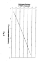
- Fig. 2 is a diagram for illustrating a relationship between a forming speed of a dielectric layer and the hydrogen content of the dielectric layer;
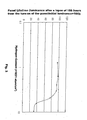
- Fig. 3 is a diagram for illustrating a relationship between the hydrogen content of the dielectric layer and a panel lifetime (the percentage of luminance deterioration with respect to that of initial luminance after a lapse of 168 hours from the turn-on of the panel);
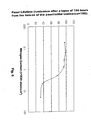
- Fig. 4 is a diagram for illustrating a relationship between the forming speed of the dielectric layer and the nitrogen content of the dielectric layer; and
- Fig. 5 is a diagram for illustrating a relationship between the nitrogen content of the dielectric layer and the panel lifetime (the percentage of luminance deterioration with respect to that of initial luminance after a lapse of 168 hours from the turn-on of the panel).
-
- The gas discharge panel according to the present invention has at least one dielectric layer, and is not particularly limited as long as it performs display by utilizing gas discharge. For example, a PDP, PALC and the like may be mentioned as the gas discharge panel.
- According to the present invention, the dielectric layer contains SiO2 as a main component and is composed of a material containing hydrogen of 5×10²¹ atom/cm3 or less and/or nitrogen of 3×10²⁰ atom/cm3 or less.
- Here, the main component means that a content ratio of SiO2 in the dielectric layer is 50 wt% or higher, more preferably a content ratio is 90 wt% or higher (the maximum ratio is 100 wt%). Components except SiO2 include hydrogen, nitrogen, carbon, phosphorus, boron and others. Among them, phosphorus and/or boron may be intentionally added to the dielectric layer for the purpose of controlling the film stress and etching speed of the dielectric layer. The concentration of phosphorus and boron is preferably 10 wt% or less, more preferably 8 wt% or less (the minimum ratio is 0 wt%).
- According to the present invention, the hydrogen content of the dielectric layer is 5×10²¹ atom/cm3 or less and/or the nitrogen content thereof is 3×10²⁰ atom/cm3 or less. The reason for defining the range of the hydrogen and nitrogen content will be hereinafter described by taking the PDP as an example.
- Fig. 2 is a diagram for illustrating a relationship between the forming speed of the dielectric layer and the hydrogen content of the dielectric layer. It is understood from Fig. 2 that the faster the layer forming speed is, the higher the hydrogen content is.
- Fig. 3 is a diagram for illustrating a relationship between the hydrogen content of the dielectric layer and a panel lifetime (the percentage of luminance deterioration with respect to that of initial luminance after a lapse of 168 hours from the turn-on of the panel). It is understood from Fig. 3 that the panel lifetime becomes sharply shorter when the hydrogen content of the dielectric layer exceeds a certain amount.
- As understood from Figs. 2 and 3, the hydrogen content of the dielectric layer to be formed needs to be within a certain range for rapidly forming the dielectric layer while prolonging the panel lifetime. The certain amount of hydrogen is 5×10²¹ atom/cm3 or less, more preferably in the range of 1×10²¹ to 3×10²¹ atom/cm3.
- Fig.4 is a diagram for illustrating a relationship between the forming speed of the dielectric layer and the nitrogen content of the dielectric layer, and Fig. 5 is a diagram for illustrating a relationship between the nitrogen content of the dielectric layer and the panel lifetime (the percentage of luminance deterioration with respect to that of initial luminance after a lapse of 168 hours from the turn-on of the panel). The same tendency can be seen for the case of nitrogen in Figs. 4 and 5, as in the case of hydrogen in Figs. 2 and 3.
- As understood from Figs. 4 and 5, the nitrogen content of the dielectric layer to be formed needs to be within a certain range for rapidly forming the dielectric layer while prolonging the panel lifetime. The certain amount of nitrogen is 3×10²⁰ atom/cm3 or less, more preferably in the range of 1×10¹⁹ to 1×10²⁰ atom/cm3.
- Accordingly, it is preferred that the hydrogen content is 5×10²¹ atom/cm3 or less and the nitrogen content is 3×10²⁰ atom/cm3 or less. A more preferable combination is a hydrogen content of 1×10²¹ to 5×10²¹ atom/cm3 and a nitrogen content of 1×10¹⁹ to 3×10²⁰ atom/cm3. A still more preferable combination is a hydrogen content of 1×10²¹ to 3×10²¹ atom/cm3 and a nitrogen content of 1×10¹⁹ to 1×10²⁰ atom/cm3.
- In Figs. 3 to 5, the dielectric layer is formed by a plasma CVD method under the conditions that a susceptor area is set to 2000 cm3, a RF output is set to 2000 W and a flow rate of SiH4 gas/N2O gas is set to 1/10, except that the flow rate of SiH4 gas varies from 100 to 2000 cm3. In Figs. 3 and 5, the measurement of the panel lifetime is performed as follows and the construction of the PDP is as follows.
- Display electrode: a width of transparent electrodes of 300 µm and that of bus electrodes of 100 µm
Discharge gap between display electrodes: 100 µm
The thickness of the dielectric layer: 10 µm
The height of barrier ribs: 100 µm
Discharge gas: Ne-Xe (5%)
Gas pressure: 500 Torr
The thickness of a phosphor layer: 20 µm
Phosphor material for red: (Y, Gd)BO3:Eu3+
Phosphor material for green: Zn2SiO4:Mn2+
Phosphor material for blue: BaMgAl10O17 : Eu2+ - An exemplary dielectric layer formed by the plasma CVD method is described above. However, a vapor phase growth method such as a CVD method except for the plasma CVD method, a sputtering, a vapor deposition or the like can be employed as long as the dielectric layer having the above specified hydrogen and/or nitrogen content can be formed. In the present invention; the plasma CVD method is preferably employed from the viewpoint of controlling warpage of the substrate and lowering cost.
- Material gas to be used for forming the dielectric layer by means of the plasma CVD method includes a silicon source such as silane: SiH4, tetraethoxysilane: Si(OC2H5)4, methyltrimethoxysilane: CH3Si (OCH3)3 or the like and a non-silicon source such as N2O CO2, CO, H2O, O2 or the like.
- Layer forming conditions such as susceptor area: 2000 to 15000 cm2, RF output: 2000 to 20000 W, temperature: 360 to 450°C, pressure: 2 to 3 Torr and the like may be mentioned for forming the dielectric layer by means of the plasma CVD method, but the above values may vary depending on the size of the substrate desirable for forming the dielectric layer and the property of the dielectric layer.
- The RF output/susceptor area is preferably 0.82 W/cm2 or higher, more preferably 0.9 W/cm2 or higher in order to set the hydrogen content at 5×10²¹ atom/cm3 or less and the nitrogen content at 3×10²⁰ atom/cm3 or less.
- A three electrode AC-type surface discharge PDP shown in Fig. 1 will be described below as an exemplary gas discharge panel according to the present invention capable of using a protective film. The following examples are provided only for illustrative purpose, and the invention is not limited thereto.
- A
PDP 1 shown in Fig. 1 is constituted of a front side substrate and a rear side substrate. - The
front side substrate 10 is generally comprised of a plurality of display electrodes X, Y to be paired which are formed on a glass substrate 11, adielectric layer 17 formed so as to cover the display electrodes, and aprotective film 18 formed on thedielectric layer 17 and exposed to a discharge space. - The display electrodes are comprised of
transparent electrode films 41 in the form of stripes or dots per discharge cell unit, andbus electrodes 42 laminated in stripes on an edge of thetransparent electrode films 41 for reducing the resistance of thefilms 41. Eachbus electrode 42 is narrower in width than each transparent electrode film. - The
transparent electrode film 41, may be formed using a method in which a paste containing an organic compound of a metal constituting the transparent electrode film is applied and baked, thereby forming the transparent electrode film. - The dielectric layer having the above specified hydrogen and/or nitrogen content can be used for the
dielectric layer 17. - The
rear side substrate 20 generally comprises a plurality of address electrodes A formed in stripes on aglass substrate 21, adielectric layer 24 formed so as to cover the address electrodes A, a plurality of band-shapedbarrier ribs 29 formed on thedielectric layer 24 and between adjacent address electrodes A, andphosphor layers - Each of the
barrier ribs 29 can be formed by applying a paste composed of low-melting glass and a binder on thedielectric layer 24 so as to form a film, baking the applied paste, and then cutting it by a sandblasting method with the use of a mask having a barrier rib shape. Where a photosensitive resin is used as the binder, the barrier rib can also be formed by exposing and developing the applied paste with the use of a mask having a predetermined shape, followed by baking. - The phosphor layers (28R, 28G, 28B) can be formed by applying a paste between the
barrier ribs 29 and then baking the paste in an inert atmosphere. In the paste, a particle-form phosphor is dispersed in a solution in which a binder is dissolved. - The dielectric layer having the above specified hydrogen and/or nitrogen content can be used for the
dielectric layer 24. In the rear side substrate, thebarrier rib 29 may be directly formed on theglass substrate 21 without forming the dielectric layer. - The aforesaid front side and rear side substrates (10,20) are arranged with the display electrodes (X,Y) and address electrodes A, which are placed to be adjacent to each other, opposed so that both the electrodes intersect at right angles, and a space surrounded by the
barrier ribs 29 is filled with a discharge gas, thereby to form thePDP 1. - The PDP to which the present method may be applied is not limited to the PDP shown in Fig. 1, but any PDP may be used insofar as it has a dielectric layer for covering discharge electrodes, such as an opposed discharge PDP, a transparent type PDP in which a phosphor layer is provided on a front side substrate and a PDP having a two electrode structure. Additionally, the barrier rib may be of a mesh form.
- The present invention will hereinafter be described in further detail by way of examples, but the invention is not limited thereto.
- Display electrodes comprised of transparent electrodes and bus electrodes were formed on a substrate by a known method.
- SiH4 and N2O as material gas were allowed to flow into a plasma CVD apparatus having a susceptor area of 2000 cm2 at flow rates of 900 sccm and 9000 sccm, respectively under the conditions of a RF output of 2.0 kW, a temperature of 400°C and a pressure of 3.0 Torr, whereby a 5-µm thick dielectric layer was formed at a layer forming speed of 0.75 µm per minute for covering the display electrodes.
- The hydrogen and nitrogen content of the formed dielectric layer was measured by SIMS (secondary ion mass spectrometry). As a result, the hydrogen content and the nitrogen content were 3.4×10²¹ atom/cm3 and 0.82×10²⁰ atom/cm3, respectively.
- A front side substrate was obtained by forming a MgO film having a thickness of 1.0 µm by means of a known electron beam evaporation.
- Subsequently, by means of a known method, address electrodes were formed on a substrate, a plurality of band-shaped barrier ribs were formed on the substrate and between adjacent address electrodes, and a phosphor layer was formed between the barrier ribs, whereby a rear side substrate was obtained.
- The obtained front side and rear side substrates were bonded to produce a PDP. The initial luminance of the produced PDP and the luminance thereof after a lapse of 168 hours were measured. Consequently, the luminance after the lapse of 168 hours was 94 % of the initial luminance, and a decline in luminance was suppressed.
- A dielectric layer was formed in the same manner as described above except that the RF output value was changed, and the hydrogen and nitrogen content of the dielectric layer was measured. The result is shown in Table 1.
RF output (W) Hydrogen content (×1021 atom/cm3) Nitrogen content (×1020 atom /cm3) 2900 0.8 0.06 2600 1.6 0.18 2300 2.5 0.38 2000 3.4 0.82 1700 4.9 2.1 1400 6.5 4.8 1100 9.6 21 - As seen from Table 1, an increase in the hydrogen and nitrogen content can be suppressed by increasing the RF output.
- A dielectric layer was formed at a layer forming speed of 0.71 µm per minute in the same manner as in Example 1, except that the susceptor area was set to 6700 cm2, the RF output was set to 6.0 kW and the flow rates of SiH4 and N2O were set to 3000 sccm and 30000 sccm, respectively.
- The hydrogen and nitrogen content of the formed dielectric layer was measured by SIMS (secondary ion mass spectrometry). As a result, the hydrogen content and the nitrogen content were 4.2×10²¹ atom/cm3 and 1.2×10²⁰ atom/cm3, respectively.
- A PDP was produced in the same manner as in Example 1. The initial luminance of the produced PDP and the luminance thereof after a lapse of 168 hours were measured. Consequently, the luminance after the lapse of 168 hours was 98 % of the initial luminance, and a decline in luminance was suppressed.
- A dielectric layer was formed in the same manner as described above except that the RF output value was changed, and the hydrogen and nitrogen content of the dielectric layer was measured. The result is shown in Table 2.
RF output (W) Hydrogen content (×1021 atom/cm3) Nitrogen content (×1020 atom /cm3) 7500 1.3 0.08 7000 2.1 0.3 6500 2.8 0.7 6000 4.2 1.2 5500 5.8 3.4 5000 7.1 11.2 4500 8.9 34.2 - As seen from Table 2, in the same manner as Table 2, an increase in the hydrogen and nitrogen content can be suppressed by increasing the RF output.
- When the initial luminance of the produced PDP and the luminance thereof after a lapse of 168 hours were measured at a RF output of 5.0 kW as shown in Table 2, the luminance after the lapse of 168 hours was 54 % of the initial luminance. That was, a sharp decline in luminance was observed. At this time, the layer forming speed was 0.84 µm per minute.
- According to the present invention, the hydrogen and/or nitrogen content of the dielectric layer constituting the gas discharge panel is defined within a specific content range, so that deaeration affecting the panel lifetime is suppressed. Therefore, it is possible to provide a low-priced display device with a high reliability.
Claims (6)
- A gas discharge panel including a plasma display panel (1), comprising:wherein the dielectric layer contains SiO2 as a main component and comprises a material containing hydrogen of 5×10²¹ atom/cm3 or less, and/or nitrogen of 3×10²⁰ atom/cm3 or less.a pair of substrates (10, 20) facing each other for forming a discharge space;an electrode (41, A) formed on at least one substrate; anda dielectric layer (17, 24) for covering the electrode;
- The gas discharge panel according to claim 1,
wherein the hydrogen content is in the range of 1×10²¹ to 5×10²¹ atom/cm3. - The gas discharge panel according to claim 1 or 2,
wherein the nitrogen content is in the range of 1×10¹⁹ to 3×10²⁰ atom/cm3. - A method of producing a gas discharge panel of any preceding claim, wherein the dielectric layer is formed by a vapor phase growth method.
- The method of producing a gas discharge panel according to claim 4, wherein the dielectric layer (17, 24) is formed by a plasma CVD method with the use of SiH4 and N2O as material gas.
- The method of producing a gas discharge panel according to claim 5, wherein the dielectric layer (17, 24) is formed by the plasma CVD method under conditions that a RF output/susceptor area is 0.82 W/cm2 or higher.
Applications Claiming Priority (2)
| Application Number | Priority Date | Filing Date | Title |
|---|---|---|---|
| JP2003032724A JP4034202B2 (en) | 2003-02-10 | 2003-02-10 | Gas discharge panel and manufacturing method thereof |
| JP2003032724 | 2003-02-10 |
Publications (3)
| Publication Number | Publication Date |
|---|---|
| EP1445786A2 true EP1445786A2 (en) | 2004-08-11 |
| EP1445786A3 EP1445786A3 (en) | 2005-08-31 |
| EP1445786B1 EP1445786B1 (en) | 2007-06-06 |
Family
ID=32653046
Family Applications (1)
| Application Number | Title | Priority Date | Filing Date |
|---|---|---|---|
| EP04250402A Expired - Fee Related EP1445786B1 (en) | 2003-02-10 | 2004-01-26 | Gas discharge panel and its production method |
Country Status (6)
| Country | Link |
|---|---|
| US (1) | US7061181B2 (en) |
| EP (1) | EP1445786B1 (en) |
| JP (1) | JP4034202B2 (en) |
| KR (1) | KR20040073290A (en) |
| DE (1) | DE602004006783T2 (en) |
| TW (1) | TWI229828B (en) |
Families Citing this family (9)
| Publication number | Priority date | Publication date | Assignee | Title |
|---|---|---|---|---|
| JP4151587B2 (en) * | 2004-02-26 | 2008-09-17 | ソニー株式会社 | Method for manufacturing AC-driven plasma display device |
| US20080211408A1 (en) * | 2004-08-17 | 2008-09-04 | Hiroyuki Yamakita | Plasma Display Panel and Method for Manufacturing Same |
| JP2006324076A (en) * | 2005-05-18 | 2006-11-30 | Japan Pionics Co Ltd | Glass panel, its manufacturing method, and plasma display panel using it |
| JPWO2007125600A1 (en) * | 2006-04-28 | 2009-09-10 | 日立プラズマディスプレイ株式会社 | Plasma display panel and method of manufacturing front plate thereof |
| WO2008038344A1 (en) * | 2006-09-27 | 2008-04-03 | Hitachi Plasma Display Limited | Gas discharge display device |
| WO2008078383A1 (en) * | 2006-12-25 | 2008-07-03 | Hitachi Plasma Display Limited | Substrate body structure for plasma display panel, and plasma display panel |
| JP5679622B2 (en) | 2008-01-31 | 2015-03-04 | 株式会社東芝 | Insulating film and semiconductor device using the same |
| KR20100048111A (en) * | 2008-10-30 | 2010-05-11 | 엘지전자 주식회사 | Plasma display panel and plasma display apparatus |
| US11538963B1 (en) * | 2018-02-20 | 2022-12-27 | Ostendo Technologies, Inc. | III-V light emitting device having low Si—H bonding dielectric layers for improved P-side contact performance |
Citations (3)
| Publication number | Priority date | Publication date | Assignee | Title |
|---|---|---|---|---|
| JPH06158327A (en) * | 1992-11-17 | 1994-06-07 | Canon Inc | Thin film depositing method |
| US6326064B1 (en) * | 1991-05-17 | 2001-12-04 | Lam Research Corporation | Process for depositing a SiOx film having reduced intrinsic stress and/or reduced hydrogen content |
| US6450849B1 (en) * | 1998-07-07 | 2002-09-17 | Fujitsu Limited | Method of manufacturing gas discharge display devices using plasma enhanced vapor deposition |
Family Cites Families (5)
| Publication number | Priority date | Publication date | Assignee | Title |
|---|---|---|---|---|
| US6184163B1 (en) * | 1998-03-26 | 2001-02-06 | Lg Electronics Inc. | Dielectric composition for plasma display panel |
| JP2000357462A (en) * | 1998-10-23 | 2000-12-26 | Sony Corp | Plane plasma discharge display device and its driving method |
| JP2001189136A (en) * | 1999-10-19 | 2001-07-10 | Matsushita Electric Ind Co Ltd | Plasma display device and its production |
| JP2001155647A (en) | 1999-11-30 | 2001-06-08 | Akt Kk | Gas discharge display device and its manufacturing method |
| JP4698077B2 (en) * | 2001-07-18 | 2011-06-08 | パナソニック株式会社 | Plasma display panel and manufacturing method thereof |
-
2003
- 2003-02-10 JP JP2003032724A patent/JP4034202B2/en not_active Expired - Fee Related
- 2003-12-19 TW TW092136209A patent/TWI229828B/en not_active IP Right Cessation
- 2003-12-22 US US10/740,818 patent/US7061181B2/en not_active Expired - Fee Related
-
2004
- 2004-01-05 KR KR1020040000236A patent/KR20040073290A/en not_active Application Discontinuation
- 2004-01-26 EP EP04250402A patent/EP1445786B1/en not_active Expired - Fee Related
- 2004-01-26 DE DE602004006783T patent/DE602004006783T2/en not_active Expired - Fee Related
Patent Citations (3)
| Publication number | Priority date | Publication date | Assignee | Title |
|---|---|---|---|---|
| US6326064B1 (en) * | 1991-05-17 | 2001-12-04 | Lam Research Corporation | Process for depositing a SiOx film having reduced intrinsic stress and/or reduced hydrogen content |
| JPH06158327A (en) * | 1992-11-17 | 1994-06-07 | Canon Inc | Thin film depositing method |
| US6450849B1 (en) * | 1998-07-07 | 2002-09-17 | Fujitsu Limited | Method of manufacturing gas discharge display devices using plasma enhanced vapor deposition |
Non-Patent Citations (2)
| Title |
|---|
| IDRIS I ET AL: "FILM CHARACTERISTICS OF LOW-TEMPERATURE PLASMA-ENHANCED CHEMICAL VAPOR DEPOSITION SILICON DIOXIDE USING TETRAISOCYANATESILANE AND OXYGEN" JAPANESE JOURNAL OF APPLIED PHYSICS, PUBLICATION OFFICE JAPANESE JOURNAL OF APPLIED PHYSICS. TOKYO, JP, vol. 37, no. 12A, PART 1, December 1998 (1998-12), pages 6562-6568, XP000927326 ISSN: 0021-4922 * |
| PATENT ABSTRACTS OF JAPAN vol. 018, no. 490 (C-1249), 13 September 1994 (1994-09-13) & JP 06 158327 A (CANON INC), 7 June 1994 (1994-06-07) * |
Also Published As
| Publication number | Publication date |
|---|---|
| US7061181B2 (en) | 2006-06-13 |
| US20040155585A1 (en) | 2004-08-12 |
| TW200415538A (en) | 2004-08-16 |
| DE602004006783T2 (en) | 2007-10-11 |
| TWI229828B (en) | 2005-03-21 |
| EP1445786A3 (en) | 2005-08-31 |
| DE602004006783D1 (en) | 2007-07-19 |
| JP4034202B2 (en) | 2008-01-16 |
| JP2004247068A (en) | 2004-09-02 |
| EP1445786B1 (en) | 2007-06-06 |
| KR20040073290A (en) | 2004-08-19 |
Similar Documents
| Publication | Publication Date | Title |
|---|---|---|
| US6450849B1 (en) | Method of manufacturing gas discharge display devices using plasma enhanced vapor deposition | |
| CN100499012C (en) | Plasma display panel | |
| EP1388878B1 (en) | Gas discharge panel substrate assembly | |
| CN100376011C (en) | Plasma display panel | |
| KR100723752B1 (en) | Production method for plasma display panel excellent in luminous characteristics | |
| US7061181B2 (en) | Gas discharge panel and its production method | |
| EP0935276B1 (en) | Gas discharge panel and gas light-emitting device | |
| JP2003173738A (en) | Protection film for plasma display panel | |
| US7439675B2 (en) | Plasma display panel having a magnesium oxide protective film and method for producing same | |
| KR100560458B1 (en) | Plasma display panel | |
| JP2002373588A (en) | Plasma display panel and its manufacturing method | |
| US20060082301A1 (en) | Image display | |
| JP2004047193A (en) | Plasma display panel | |
| JP4360926B2 (en) | Plasma display panel | |
| JP4715037B2 (en) | Plasma display panel and manufacturing method thereof | |
| EP2037480A1 (en) | Plasma display panel and manufacturing method therefor | |
| JP2004006426A (en) | Method of manufacture gas discharge display device | |
| JP2002373589A (en) | Gas discharge panel and its manufacturing method | |
| KR20080020822A (en) | Plasma display panel | |
| JP2006324254A (en) | Manufacturing method of gas discharge display device | |
| JP2004335339A (en) | Plasma display panel and its manufacturing method | |
| KR20030046062A (en) | Plasma Display Panel and Fabricating Method Thereof | |
| KR20060057848A (en) | Display panel, the fabrication method thereof, and panel assembly using the such | |
| KR20040085763A (en) | Plasma display panel and method of fabricating the same | |
| JP2011014444A (en) | Plasma display and method of manufacturing the same |
Legal Events
| Date | Code | Title | Description |
|---|---|---|---|
| PUAI | Public reference made under article 153(3) epc to a published international application that has entered the european phase |
Free format text: ORIGINAL CODE: 0009012 |
|
| AK | Designated contracting states |
Kind code of ref document: A2 Designated state(s): AT BE BG CH CY CZ DE DK EE ES FI FR GB GR HU IE IT LI LU MC NL PT RO SE SI SK TR |
|
| AX | Request for extension of the european patent |
Extension state: AL LT LV MK |
|
| PUAL | Search report despatched |
Free format text: ORIGINAL CODE: 0009013 |
|
| AK | Designated contracting states |
Kind code of ref document: A3 Designated state(s): AT BE BG CH CY CZ DE DK EE ES FI FR GB GR HU IE IT LI LU MC NL PT RO SE SI SK TR |
|
| AX | Request for extension of the european patent |
Extension state: AL LT LV MK |
|
| RIC1 | Information provided on ipc code assigned before grant |
Ipc: 7C 23C 16/44 B Ipc: 7C 23C 16/40 B Ipc: 7H 01J 17/02 B Ipc: 7H 01J 17/49 A |
|
| 17P | Request for examination filed |
Effective date: 20060222 |
|
| AKX | Designation fees paid |
Designated state(s): DE FR GB |
|
| GRAP | Despatch of communication of intention to grant a patent |
Free format text: ORIGINAL CODE: EPIDOSNIGR1 |
|
| GRAS | Grant fee paid |
Free format text: ORIGINAL CODE: EPIDOSNIGR3 |
|
| GRAA | (expected) grant |
Free format text: ORIGINAL CODE: 0009210 |
|
| AK | Designated contracting states |
Kind code of ref document: B1 Designated state(s): DE FR GB |
|
| REG | Reference to a national code |
Ref country code: GB Ref legal event code: FG4D |
|
| REF | Corresponds to: |
Ref document number: 602004006783 Country of ref document: DE Date of ref document: 20070719 Kind code of ref document: P |
|
| ET | Fr: translation filed | ||
| PLBE | No opposition filed within time limit |
Free format text: ORIGINAL CODE: 0009261 |
|
| STAA | Information on the status of an ep patent application or granted ep patent |
Free format text: STATUS: NO OPPOSITION FILED WITHIN TIME LIMIT |
|
| 26N | No opposition filed |
Effective date: 20080307 |
|
| REG | Reference to a national code |
Ref country code: FR Ref legal event code: CA Ref country code: FR Ref legal event code: CD |
|
| PGFP | Annual fee paid to national office [announced via postgrant information from national office to epo] |
Ref country code: DE Payment date: 20090123 Year of fee payment: 6 |
|
| PGFP | Annual fee paid to national office [announced via postgrant information from national office to epo] |
Ref country code: GB Payment date: 20090121 Year of fee payment: 6 |
|
| PGFP | Annual fee paid to national office [announced via postgrant information from national office to epo] |
Ref country code: FR Payment date: 20090113 Year of fee payment: 6 |
|
| GBPC | Gb: european patent ceased through non-payment of renewal fee |
Effective date: 20100126 |
|
| REG | Reference to a national code |
Ref country code: FR Ref legal event code: ST Effective date: 20100930 |
|
| PG25 | Lapsed in a contracting state [announced via postgrant information from national office to epo] |
Ref country code: FR Free format text: LAPSE BECAUSE OF NON-PAYMENT OF DUE FEES Effective date: 20100201 |
|
| PG25 | Lapsed in a contracting state [announced via postgrant information from national office to epo] |
Ref country code: DE Free format text: LAPSE BECAUSE OF NON-PAYMENT OF DUE FEES Effective date: 20100803 |
|
| PG25 | Lapsed in a contracting state [announced via postgrant information from national office to epo] |
Ref country code: GB Free format text: LAPSE BECAUSE OF NON-PAYMENT OF DUE FEES Effective date: 20100126 |