BACKGROUND OF THE INVENTION
1. Field of the Invention
The present invention relates to a method of
generating mask distortion data used in a lithography
step in producing a semiconductor device, an exposure
method using the same, and a method of producing a
semiconductor device using the same.
2. Description of the Related Art
Masks having a common point are used in lithography
using charged particles, such as an electron beam (EB)
and an ion beam, under development as next generation
lithography (NGL) which follows after present
photolithography (wavelengths of 248 nm and 193 nm are
dominant) used in mass production of a semiconductor
device.
The common point is that, by deeply etching a
substrate to be a mask from the back surface side to
leave a thin film (membrane) having a thickness of 10 nm
to 10 µm or so, mask blanks as a mask before being formed
a pattern are formed and a pattern to be transferred are
arranged to the obtained thin film.
Since such a mask includes a membrane region having
low mechanical strength, not to mention a method of
forming a pattern of high positional accuracy (IP: image
placement), a technique of measuring distortion of a mask
and correcting an IP error by using the information is
important.
Proximity electron lithography (PEL) and electron
projection lithography (EPL) are particularly dominant
among NGL using an EB.
General explanations on an electronic optical
system and mask of the two methods are described on the
PEL in "Journal of Vacuum Science and Technology", B17, p.
2897 (1999) by T. Utsumi and on the EPL in "Japanese
Journal of Applied Physics", 34, p. 6658 (1999) by H. C.
Pfeiffer.
Among masks used in the above PEL and EPL, (1)
those having a transfer pattern formed by an opening of a
membrane are called stencil masks (for example, refer to
"Japanese Journal of Applied Physics", 34, p. 6658 (1999)
by H. C. Pfeiffer) and (2) those having a transfer
pattern formed by a scattering body, such as a metal thin
film, are called a scattering membrane mask (for example,
refer to "Journal of Vacuum Science and Technology", B15,
P. 2130 (1997) by L. R. Harriott).
The former stencil mask is used for both of the PEL
and EPL, while the scattering membrane mask cannot be
used for the PEL. It is because the PEL generally uses a
low speed EB of several keV or less and the incident EB
on the membrane is all absorbed.
Since these masks include a membrane region having
low mechanical strength, a mask structure of not
configuring the overall mask region with one membrane but
configuring with a large number of small sectional
membranes divided by a lattice shaped beam has been
proposed. For example, a PEL mask is described in the
Japanese Unexamined Patent Publication No. 2003-59819 and
an EPL mask is described in the U.S. Patent No. 5523580.
FIG. 1 is a schematic perspective view of a mask
having a lattice shaped beam as above. The lattice shaped
beam 100b composes a plurality of recessed portions 100a
and, thereby, a thin film (membrane) 102 is divided to a
large number of small sectional membranes. In the thin
film 102, small regions sectionalized by the beam 100b
respectively become pattern regions PA formed with a
pattern.
As a method of producing a mask having the above
beam structure, a method of using wet etching by an
alkali solution of KOH, etc. and a method of using
reactive ion etching are described in the U.S. Patent No.
6428937.
FIG. 2A is a schematic sectional view of the above
stencil mask.
It has a multilayer structure of forming on a
silicon substrate 110 a buried oxide layer 111 as an
interlayer having an etching stopper function and a
silicon thin film (SOI: silicon on insulator) 112 to be a
membrane. A part of the substrate 110 corresponding to
the membrane is formed with recessed portions 110a
sectionalized to be a lattice shape by being etched from
the back surface to configure the lattice shaped beam
110b.
Also, the SOI layer 112 is formed with through
holes P along a mask pattern.
FIG. 2B is a schematic sectional view of the above
scattering membrane mask.
A silicon nitride thin film 121 to be a membrane is
formed on the silicon substrate 120, and a part of the
substrate 120 corresponding to the membrane is formed
with recessed portions 120a sectionalized to be a lattice
shape by being etched from the back surface to compose
the lattice shaped beam 120b.
Also, a scattering body pattern 124, for example,
made by a chrome film 122 having a film thickness of 10
nm and a tungsten film 123 having a film thickness of 50
nm is formed along the mask pattern.
As a method of transferring a pattern of a mask
used in the PEL and EPL on a wafer at a high accuracy, a
method of measuring distortion of the mask and correcting
it when transferring can be considered.
This concept itself is not new and has been also
used in photolithography, and IP accuracy of a produced
photomask is measured routinely by a coordinate measuring
device called "LMS IPRO" made by LEICA Corporate or
"lightwave XY-6i" made by Nikon Corporation.
For example, when a magnification error of 3 ppm is
measured on a mask pattern, the error can be corrected by
finely adjusting an optical system of an exposure
apparatus when exposing the photomask with a stepper or a
scanner.
However, in lithography using charged particles,
such as the PEL and EPL, since incident particles can be
deflected at high accuracy and high speed by an
electrostatic / magnetic field lens, it is considered
that correction at a higher accuracy becomes possible.
In the case of the PEL, a main deflection lens and
a sub deflection lens are combined to deflect the EB.
Here, by scanning the EB by the main deflection lens on
the mask region and changing an incident angle of the EB
by the sub deflection lens in real time, distortion of
the mask can be corrected (for example, refer to the U.S.
Patent No. 4334156).
On the other hand, in the case of the EPL,
individual membrane sectionalized by the beam 100b as
shown in FIG. 1 is defined as a subfield, and a method of
transferring the subfield by EB irradiation at one time
on a wafer and forming a device pattern by successively
connecting the subfields on the wafer is applied. For
example, a method of correcting distortion for each
subfield is disclosed in the Japanese Unexamined Patent
Publication No. 2000-124114.
In the case of the PEL, there is an advantage that,
by giving information of distortion over the whole mask
region as a map and compensating between measurement data
points by a function of a higher order, distortion of a
higher order can be corrected in addition to linear
distortion of magnification, rotation and orthogonality.
On the other hand, in the case of the EPL, only
linear distortion of each subfield can be corrected.
In either case of the above PEL and EPL, accurate
measurement of mask distortion is important at first.
However, a mark for a coordinate measuring device, such
as the above LMS IPRO, generally cannot be arranged on a
region arranged with a device pattern.
Accordingly, in the case of a photomask, a mark for
coordinate measurement is arranged on a part
corresponding to a so called scribe line, that is, a chip
periphery region (a margin region when detaching a chip
on a wafer by dicing).
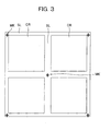
FIG. 3 is an example of a layout of arranging the
marks for coordinate measurement on the scribe line.
Coordinate measurement marks MK are arranged on the
scribe line SL for sectionalizing the chip region.
Reliability of distortion data becomes higher when
increasing the number of coordinate measurement marks to
increase measurement points and, furthermore, uniformly
distributing them allover the mask region, however, due
to the limit that the coordinate measurement marks can be
arranged only on the scribe line, only limited number of
coordinate measurement marks could be used as shown in
FIG. 3.
In the EPL, as shown in FIG. 1, by utilizing the
fact that the mask is originally divided to small
sectionalized subfields (typically, about 1 mm square),
it has been proposed to arrange coordinate measurement
marks on a beam between the subfields (refer to the U.S.
Patent No. 6040095).
As explained above, since only linear distortion of
subfields is corrected in the EPL, it is sufficient to
measure marked coordinates at four corners of each
subfield. The marks on the beam are not transferred to
the wafer, so that it is possible to increase measurement
points and improve accuracy of distortion measurement.
The U.S. Patent No. 6040095 discloses a formation method
and arrangement method of the marks on the beam.
In the method described in the above U.S. Patent No.
6040095, however, accuracy of measuring distortion is
limited, so it is difficult to use the method in device
production using the PEL and EPL.
Namely, the method of the U.S. Patent No. 6040095
stands on an assumption that beam marks and an actual
device pattern in a membrane displace by the same
distortion function, so that disposition of the latter
can be corrected based on measurement data of the former.
However, this assumption is physically not self-evident,
moreover, it became clear that it stood only
approximately in our actual measurement.
Accordingly, more accurate measurement of
distortion of the membrane is not possible only by
measuring the beam marks. Particularly, in the case of
the PEL, since a pattern on the mask is transferred on
the wafer without reduction, an effect of a distortion
data error is supposed to be larger than that in the case
of the EPL. Thus, it is difficult to apply the method
described in the U.S. Patent No. 6040095 as it is.
SUMMARY OF THE INVENTION
An object of the present invention is to provide a
method of generating mask distortion data capable of
improving accuracy of measuring distortion, an exposure
method for more accurately correcting mask distortion for
exposure by using the same, and a method of producing a
semiconductor device using the same.
To attain the above object, there is provided a
method of generating mask distortion data of a first thin
film of a production mask formed with first positional
accuracy measurement marks and having at least one first
thin film formed with a transmittance portion and a
blocking portion of a charged particle beam of a
predetermined pattern, comprising steps of obtaining a
positional accuracy measurement mask by forming second
positional accuracy measurement marks at substantially
same positions as those of the first positional accuracy
measurement marks on mask blanks having at least one
second thin film, and forming third positional accuracy
measurement marks on the second thin film; measuring
positions of the second positional accuracy measurement
marks and the third positional accuracy measurement marks
of the positional accuracy measurement mask; calculating
a correlation function between positions of the second
positional accuracy measurement marks and the third
positional accuracy measurement marks of the positional
accuracy measurement mask; measuring positions of the
first positional accuracy measurement marks of the
production mask; and generating mask distortion data on
the first thin film of the production mask from positions
of the first positional accuracy measurement marks of the
production mask by using the correlation function.
The generation method of mask distortion data of
the present invention as above is a method of generating
mask distortion data of a first thin film of a production
mask formed with first positional accuracy measurement
marks and having at least one first thin film formed with
a transmittance portion and a blocking portion of a
charged particle beam of a predetermined pattern.
A positional accuracy measurement mask is obtained
by forming second positional accuracy measurement marks
at substantially same positions as those of the first
positional accuracy measurement marks on mask blanks
having at least one second thin film, and forming third
positional accuracy measurement marks on the second thin
film.
Next, positions of the second positional accuracy
measurement marks and the third positional accuracy
measurement marks of the positional accuracy measurement
mask are measured, and a correlation function between
positions of the second positional accuracy measurement
marks and the third positional accuracy measurement marks
of the positional accuracy measurement masks is
calculated.
Next, positions of the first positional accuracy
measurement marks of the production mask are measured.
Next, mask distortion data on the first thin film
of the production mask is generated from positions of the
first positional accuracy measurement marks of the
production mask by using the correlation function.
To attain the above object, according to the
present invention, there is provided an exposure method
for exposing a pattern by using a production mask formed
with first positional accuracy measurement marks and
having at least one first thin film formed with a
transmittance portion and a blocking portion of a charged
particle beam of the predetermined pattern, comprising
steps of obtaining a positional accuracy measurement mask
by forming second positional accuracy measurement marks
at substantially same positions as those of the first
positional accuracy measurement marks on mask blanks
having at least one second thin film, and forming third
positional accuracy measurement marks on the second thin
film; measuring positions of the second positional
accuracy measurement marks and the third positional
accuracy measurement marks of the positional accuracy
measurement mask; calculating a correlation function
between positions of the second positional accuracy
measurement marks and the third positional accuracy
measurement marks of the positional accuracy measurement
mask; measuring positions of the first positional
accuracy measurement marks of the production mask;
generating mask distortion data on the first thin film of
the production mask from positions of the first
positional accuracy measurement marks of the production
mask by using the correlation function; and exposing the
pattern by using the production mask while correcting
mask distortion of the first thin film based on the mask
distortion data.
In the exposure method of the present invention as
above, mask distortion data is generated by the above
generation method of mask distortion data of the present
invention, then, a pattern is exposed by using the
production mask while correcting mask distortion on the
first thin film based on the mask distortion data.
To attain the above object, a method of producing a
semiconductor device including a step of exposing a
pattern on a wafer to be exposed by using a production
mask formed with first positional accuracy measurement
marks and having at least one first thin film formed with
a transmittance portion and a blocking portion of a
charged particle beam of the predetermined pattern,
comprising steps of obtaining a positional accuracy
measurement mask by forming second positional accuracy
measurement marks at substantially same positions as
those of the first positional accuracy measurement marks
on mask blanks having at least one second thin film, and
forming third positional accuracy measurement marks on
the second thin film; measuring positions of the second
positional accuracy measurement marks and the third
positional accuracy measurement marks of the positional
accuracy measurement mask; calculating a correlation
function between positions of the second positional
accuracy measurement marks and the third positional
accuracy measurement marks of the positional accuracy
measurement mask; measuring positions of the first
positional accuracy measurement marks of the production
mask; generating mask distortion data on the first thin
film of the production mask from positions of the first
positional accuracy measurement marks of the production
mask by using the correlation function; and exposing the
pattern on the wafer to be exposed by using the
production mask while correcting mask distortion of the
first thin film based on the mask distortion data.
The production method of a semiconductor device of
the present invention as above includes, after generating
mask distortion data by the generation method of mask
distortion data of the present invention as above, a step
of exposing a pattern on a wafer to be exposed by using
the production mask while correcting mask distortion on
the first thin film based on the mask distortion data.
BRIEF DESCRIPTION OF DRAWINGS
These and other objects and features of the present
invention will become clearer from the following
description of the preferred embodiments given with
reference to the attached drawings, in which:
DESCRIPTION OF THE PREFERRED EMBODIMENT
Below, a generation method of mask distortion data
according to the present embodiment, an exposure method
using the same and a production method of a semiconductor
device will be explained with reference to the drawings.
First Embodiment
The present embodiment relates to a method of
generating distortion data of a mask, such as a PEL mask,
for exposing by using a low energy electron beam
proximity projection lithography (LEEPL) transfer
apparatus, which is a method of generating mask
distortion data according to a pattern formed on a first
thin film of a production mask formed with first
positional accuracy measurement marks and having at least
one layer of first thin film formed with a transmittance
portion and blocking portion of a charged particle beam
of a predetermined pattern.
Also, the present embodiment relates to a method of
exposing a pattern by correcting distortion based on the
mask distortion data by using the above mask.
FIG. 4 is a flowchart of a generation method of
mask distortion data according to the present embodiment
and an exposure method using the same.
First, as a first step ST11, a positional accuracy
measurement mask is formed by mask blanks having at least
one layer of second thin film.
Here, it is assumed that except that positional
accuracy measurement marks are formed on the second thin
film instead of a pattern formed on the first thin film,
the configuration of the positional accuracy measurement
mask is the same as that of the production mask. Namely,
the first thin film and the second thin film have the
same layer configuration, and the positional accuracy
measurement mask is formed with second positional
accuracy measurement marks at substantially the same
positions as those of the first positional accuracy
measurement marks, and the second thin film is not formed
with a pattern but third positional accuracy measurement
marks.
Next, in a second step ST12, positions of the
second positional accuracy measurement marks and the
third positional accuracy measurement marks of the
positional accuracy measurement mask are measured by a
coordinate measurement device, such as an LMS IPRO. In a
third step ST13, IP data of the second positional
accuracy measurement marks is obtained. In a fourth step
ST14, IP data of the third positional accuracy
measurement marks is obtained.
Next, in a fifth step ST15, a correlation function
between the IP data of the second positional accuracy
measurement marks and the IP data of the third positional
accuracy measurement marks is calculated.
Here, the first step ST11 to the fifth step ST15
can be replaced by a finite element simulation modeling
the mask.
On the other hand, in a sixth step ST16, a
production mask is formed by a mask blanks having at
least one layer of a first thin film.
Here, the production mask is formed with first
positional accuracy measurement marks as explained above,
and a transmittance portion and blocking portion of a
charged particle beam of a predetermined pattern are
formed on the first thin film.
Next, in a seventh step ST17, in the same way as in
the second step ST12, positions of the first positional
accuracy measurement marks of the production mask are
measured by a coordinate measurement device, such as an
LMS IPRO. In an eighth step ST18, IP data of the first
positional accuracy measurement marks is obtained.
Next, in a ninth step ST19, by using the
correlation function between the IP data of the second
positional accuracy measurement marks and the IP data of
the third positional accuracy measurement marks obtained
in the fifth step ST15, mask distortion data of the first
thin film of the production mask is generated from the IP
data of the first positional accuracy measurement marks
obtained in the seventh step ST17.
From the above, mask distortion data on a pattern
formed on the first thin film of the production mask
formed with the first positional accuracy measurement
marks is generated.
Furthermore, to expose the pattern by using the
above production mask, the method below is performed.
Namely, in a tenth step ST20, a condition of an
exposure apparatus, such as an EB deflection condition
when exposing a pattern by using the production mask, is
corrected based on the mask distortion data of the first
thin film of the obtained production mask.
Next, in an eleventh step ST21, by using the
corrected condition of the exposure apparatus obtained in
the tenth step ST20, pattern exposure is performed while
correcting the mask distortion.
From the above, a pattern formed on the first thin
film of the production mask formed with the first
positional accuracy measurement marks is exposed.
Next, the configuration of a production mask and a
positional accuracy measurement mask according to the
generation method of the mask distortion data according
to the present embodiment and the exposure method will be
explained.
First, the production mask will be explained.
FIG. 5A is a plan view of an appearance of the
above production mask.
The production mask has a square mask region having
sides of 2L. The mask region is divided to four squares A
to D respectively having sides of L, and each of them
becomes one complementary mask.
FIG. 5B is an enlarged view of a center portion of
the mask region of FIG. 5A. A recessed portion 10a to be
a small sectionalized membrane region having sides of L10a
is divided by a lattice shaped beam 10b having a width of
L10b. A pattern formed respectively on the small
sectionalized membrane regions is omitted.
For example, a side L10a of the recessed portion 10a
is 1050 µm, the width L10b of the beam is 200 µm, and a
side 2L of the overall mask region is 40 mm.
Also, FIG. 6 is a schematic sectional view of the
above production mask.
It has the multilayer configuration wherein a
buried oxide film (BOX) 11 as an interlayer having an
etching stopper function and a first silicon thin film
(SOI: silicon on insulator) 12 to be a membrane are
formed on a silicon substrate 10. A part of the silicon
substrate 10 corresponding to the membrane is etched from
the back surface to be formed with recessed portion 10a
sectionalized to be a lattice shape to configure the
lattice shaped beam 10b.
The SOI layer 12 on the region of the recessed
portions 10a sectionalized by the lattice shaped beam 10b
is formed through holes P along a mask pattern.
Here, on a region of forming the lattice shaped
beam 10b for sectionalizing the recessed portions 10a to
be small sectionalized membrane regions, first positional
accuracy measurement marks MK1 are formed on the SOI
layer 10.
Also, FIG. 7 is a plan view of a layout of
positional accuracy measurement marks of the above
production mask.
The first positional accuracy measurement marks MK1
are formed on a region for forming the lattice shaped
beam 10b for sectionalizing the recessed portions 10a to
be small sectionalized membrane regions.
Here, the first positional accuracy measurement
marks MK1 may be formed on the SOI layer 12 positioned
above the beam 10b as shown in FIG. 6 or on the surface
of the beam 10b on the opposite surface from the surface
to be formed the SOI layer 12 as far as they are on the
lattice shaped beam 10b formation region. It can be
selected, for example, in accordance with the posture at
the time of measuring positions of the first positional
accuracy measurement marks MK1.
The through holes P along the mask pattern shown in
FIG. 6 are omitted in FIG. 7.
On the other hand, the positional accuracy
measurement mask has the same configuration as that of
the above production mask, but is different in the point
that third positional accuracy measurement marks MK3 are
formed instead of through holes along the mask pattern on
the SOI layer on the recessed portion 10a.
The positional accuracy measurement mask will be
explained with reference to FIG. 6 and FIG. 7.
Namely, a BOX layer 11 and a second thin film (SOI)
12' are stacked on a silicon substrate 10, a part of the
silicon substrate corresponding to a membrane is etched
from the back surface to form recessed portions 10a
sectionalized to be a lattice shape, so a lattice shaped
beam 10b is configured.
Here, as shown in FIG. 7, second positional
accuracy measurement marks MK2 are formed on the
formation region of the lattice shaped beam 10b in the
same way as in the first positional accuracy measurement
marks MK1.
Also, the SOI layer 12' on the region of the
recessed portions 10a sectionalized by the lattice shaped
beam 10b is formed third positional accuracy measurement
marks MK3. Detailed illustration is omitted in FIG. 7.
As the first positional accuracy measurement marks
MK1 and the second positional accuracy measurement marks
MK2, for example, twenty marks are formed on the
formation region of the beam 10b around the region
divided as one recessed portion. In this way, much larger
number of marks can be arranged than the number of marks
in the related art shown in FIG. 3, so that distortion of
a higher order can be measured by this and terms of a
higher order other than linear components can be
corrected.
Also, as the third positional accuracy measurement
marks MK3, for example, 3×3 number of square marks by 6
µm by 6 µm are arranged at pitches of 500 µm in each
recessed portion 10a sectionalized to be a lattice shape.
Next, a method of producing a production mask and a
positional accuracy measurement mask configured as above
will be explained. For example, a method described in
detail in the Japanese Unexamined Patent Publication No.
2003-59819 and an application (the Japanese Patent
Application No. 2001-370600) by the present inventors can
be preferably applied.
In a production mask, except that through holes are
formed along the mask pattern of the SOI layer on the
region of the recessed portions 10a, and the third
positional accuracy measurement marks MK3 are formed on
the positional accuracy measurement mask, the production
mask and the positional accuracy measurement mask can be
formed in the same way.
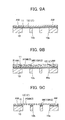
First, as shown in FIG. 8A, for example, an SOI
wafer formed by stacking a buried oxide film (BOX layer)
11 as an interlayer having an etching stopper function
and a silicon layer (SOI layer) 12 to be a membrane on a
silicon substrate 10 is prepared. The whole surface of
the SOI wafer is covered with a natural oxide film 13.
By injecting boron (B) to the SOI wafer configured
as above, an internal stress of the membrane layer is
adjusted.
Next, as shown in FIG. 8B, for example, the SOI
layer 12 is removed until reaching to the BOX layer 11 to
be a predetermined pattern on the periphery portion of
the SOI wafer so as to form alignment marks AM.
Next, as shown in FIG. 8C, a resist film (not
shown) is formed on the back surface of the silicon
substrate, openings of a pattern of a lattice shape is
formed by exposure and development, etching processing,
such as RIE (reactive ion etching), is performed to form
a recessed portion 10a reaching to the BOX layer 11 from
the back surface of the silicon substrate 10, for example,
of a pattern sectionalized to be a lattice shape. At this
time, a portion left to be a lattice shape on the silicon
substrate 10 becomes the lattice shaped beam 10b, and the
silicon substrate 10 becomes a supporting frame on the
peripheral portion of the SOI wafer.
Next, as shown in FIG. 9A, a resist film (not
shown) is removed by ashing processing, etc. and oxide
silicon on a portion exposed on the surface is removed by
wet etching by an HF solution. Namely, the natural oxide
film 13 and the BOX film 11 exposed on the bottom portion
of the recessed portion 10a are removed.
From the above, mask blanks configured by stacking
the BOX layer 11 and the SOI layer 12 on the silicon
substrate 10 wherein a recessed portion sectionalized to
be a lattice shape is formed to an extent the SOI layer
exposes from the back side of the silicon substrate 10.
Next, as shown in FIG. 9B, a resist film R is
formed on the SOI layer 12, and a pattern P is formed by
exposing, for example, by an electron beam and developing
along mask data of a mask to be formed in the method of
producing the production mask. At the same time, a
pattern for the first positional accuracy measurement
marks MK1 are also formed on the resist film R.
Next, dry etching, such as RIE, is performed by
using the resist film R as a mask, and the pattern P of
the mask to be formed on the SOI layer 12 and the first
positional accuracy measurement marks MK1 are transferred
in the method of producing the production mask.
After that, the resist film R is removed by ashing
processing, so that a mask having the configuration shown
in FIG. 9C can be produced.
On the other hand, in the method of producing a
positional accuracy measurement mask, in the same way as
in the above production method of the production mask,
mask blanks are formed by stacking the BOX layer 11 and
the SOI layer 12' on the silicon substrate 10 as shown in
FIG. 9A, and a pattern of the second positional accuracy
measurement marks MK2 and the third positional accuracy
measurement marks MK3 is obtained by exposing and
developing along the pattern of the second positional
accuracy measurement marks MK2 and the third positional
accuracy measurement marks MK3 as shown in FIG. 9B.
Next, as shown in FIG. 9C, a pattern of the second
positional accuracy measurement marks MK2 and the third
positional accuracy measurement marks MK3 are transferred
on the SOI layer 12'.
In the present embodiment, distortion data of a
production mask can be generated by a procedure shown in
the flowchart in FIG. 4 by using the production mask and
the positional accuracy measurement mask formed as above.
Mask distortion data generated as such can improve
accuracy of measuring distortion due to the reasons
explained later on.
Next, an exposure method capable of performing
pattern exposure while more accurately correcting mask
distortion when exposing a pattern by using the
production mask based on the obtained distortion data of
the production mask will be explained.
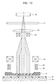
FIG. 10 is a schematic view of an exposure system
used in the LEEPL.
The exposure system comprises an electron gun 30,
an aperture 31, a condenser lens 32, a pair of main
deflection lenses (33, 34) and a pair of sub deflection
lenses (35, 36).
An electron beam EB having a current value of 5.5
µA and a beam diameter of 300 µm accelerated at an EB
acceleration voltage of 2keV emitted from the electron
gun 30 is limited by the aperture 31 and made to be a
parallel beam by the condenser lens 32.
The main deflection lenses (33, 34) deflect the
electron beam, so that the electron beam EB
perpendicularly irradiates the stencil mask 37 while
being in parallel.
The electron beam EB is incident on the stencil
mask 37 in a raster or vector scanning mode, and the main
deflection lenses (33, 34) are used for deflecting the
electron beam EB in both cases. The sub deflection lenses
(35, 36) further precisely adjust the electron beam EB
deflected by the main deflection lenses (33, 34).
The electron beam EB transmitted through the
stencil mask 37 is incident on the resist film 39
provided, for example, on a silicon wafer 38 and pattern
exposure is performed thereon.
In the present embodiment, based on the obtained
distortion data of the production mask, it is possible to
perform pattern exposure while more precisely correcting
mask distortion by using the production mask, for example,
correcting the condition of the sub deflection lenses (35,
36), and exposing under the corrected condition.
[Examples]
Here, a generation method of mask distortion data
of the present embodiment was applied to a PEL mask for
generating mask distortion data.
First, a production mask and a positional accuracy
measurement mask were formed as explained below.
As a substrate for producing mask blanks, 4 inches
(about 100 mm) of SOI wafer available on market produced
by a bonding method was used. A thickness of the wafer
substrate was 381 µm (polished on both surfaces to
improve flatness of the mask), a thickness of the BOX
layer was 400 nm, a thickness of the SOI layer was 600 nm,
and internal stress of the membrane layer was adjusted to
10 MPa by injecting boron (B) atoms of 1019/cm3.
On the SOI wafer configured as above, the
production mask and the positional accuracy measurement
mask having the configurations shown in FIG. 5 and FIG. 6
were formed by steps shown in FIG. 8A to FIG. 8C and FIG.
9A to FIG. 9C.
Here, first positional accuracy measurement marks
MK1 on the production mask and second positional accuracy
measurement marks MK2 on the positional accuracy
measurement mask were configured the same and formed on a
formation region of the beam 10b.
On the other hand, a pattern P of a mask to be
formed was transferred on the SOI layer on the region of
the recessed portions sectionalized to be a lattice shape
on the production mask, and a pattern of third positional
accuracy measurement marks were transferred on the
positional accuracy measurement mask.
In steps below, the production mask and the
positional accuracy measurement mask were adhered to an
aluminum frame shown in FIG. 11A and FIG. 11B to be used.
FIG. 11A is a plan view of the above frame, and FIG.
11B is a sectional view thereof.
A frame 20 has a ring shape having an outer
diameter of 20a and an inner diameter of 20b, and a step
20c is formed at a position of a predetermined diameter.
The inner diameter is designed to be wider than the whole
mask region having sides of 2L.
At three points on a circumference on a little
inner region of the step 20c being away by 120° from each
other, the production mask and the positional accuracy
measurement mask were respectively adhered to the above
frame with an epoxy resin.
Next, on the positional accuracy measurement mask,
positions of the second positional accuracy measurement
marks formed on a formation region of a lattice shaped
beam and the three positional accuracy measurement marks
formed on the SOI layer on the recessed portion formation
region sectionalized by the lattice shaped beam were
respectively measured by a coordinate measurement device
(LMS IPRO), and IP data of the second positional accuracy
measurement marks and IP data of the third positional
accuracy measurement marks were obtained.
Here, a mask holding cassette was newly produced to
measure positional accuracy of the positional accuracy
measurement mask and the production mask when measuring
positions by the coordinate measurement device.
FIG. 12A is a plan view of the mask holding
cassette, and FIG. 12B is a schematic sectional view when
holding a mask by the mask holding cassette.
The mask holding cassette 21 is provided with an
electrostatic chuck 21a and thereby an outer
circumference portion other than the mask region 21b (40
mm square at the center in this case) is
electrostatically chucked. And measurement is made in a
state that the SOI layer (second thin film) 12' faces
upward and the mask is held from the opposite side of the
SOI layer (second thin film) 12'. Note that in FIG. 12B,
illustration of the second positional accuracy
measurement marks is omitted.
Also, it may be configured to be provided with a
suction chuck instead of the electrostatic chuck.
Consequently, IP accuracy of marks can be measured
in a state that the stencil mask is made to be flat.
Here, measurement results of the second positional
accuracy measurement marks MK2 formed on the beam
formation region and the third positional accuracy
measurement marks MK3 formed on the SOI layer on the
region of the recessed portions sectionalized to be a
lattice shape will be explained.
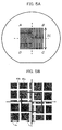
FIG. 13A is a graph of the measurement result of
the second positional accuracy measurement marks MK2
formed on the beam formation region, wherein solid lines
are made by connecting actually measured values and
broken lines indicate positions of an ideal lattice.
Note that errors are enlarged in the drawings so
that deviation from the ideal lattice is easily seen.
On the other hand, FIG. 13B is a graph of
measurement results of the third positional accuracy
measurement marks MK3 formed on the SOI layer on the
region of the recessed portions sectionalized to be a
lattice shape, wherein solid lines are made by connecting
actually measured values and broken lines indicate
positions of an ideal lattice.
As is known from the drawings, IP measurement
results of the second positional accuracy measurement
marks MK2 formed on the beam formation region and the
third positional accuracy measurement marks MK3 formed on
the SOI layer on the region of the recessed portions
sectionalized to be a lattice shape are similar and seem
to qualitatively support an idea of the related art (the
U.S. Patent No. 6040095), however, when closely analyzing
the data, a difference of about 20 nm at maximum was
found between them.
The error is 5 nm in the 1/4 reduction projection
method, such as the EPL, and 20 nm in the PEL on the
wafer. Since an error being unacceptable even in the 1/4
reduction production method is generated in the related
art, it cannot be used in the PEL as an unmagnification
method used in the present embodiment.
What described below is considered as a cause of
the error.
When the second positional accuracy measurement
marks MK2 formed on the beam formation region and the
third positional accuracy measurement marks MK3 formed on
the SOI layer on the region of the recessed portions
sectionalized to be a lattice shape are formed by the
same drawing in processing steps, an IP error thereof is
mainly regulated by accuracy of an EB plotting machine,
so the both are supposed to be similar.
However, when fixing a mask on stages of the EB
plotting machine and the coordinate measurement device,
the fixing methods are not completely the same on the two
stages, so that a shape of the mask (projections and
recesses) of the mask differs in accordance with
difference of degrees to straighten warps of the mask.
The second positional accuracy measurement marks
MK2 formed on the beam formation region basically
indicate displacement within the plane of (tilting angle
of mask substrate) x (half of substrate thickness) as
described in articles of mechanics of materials (for
example, refer to "Theory of Plates and Shells" by S. P.
Timoshenko and S. Woinowsky-Krieger).
On the other hand, the third positional accuracy
measurement marks MK3 formed on the SOI layer on the
region of the recessed portions sectionalized to be a
lattice shape follow displacement induced inside the SOI
layer when assuming that deformation of the beam around
the region of the recessed portions is constraint
displacement (boundary condition).
As explained above, the mechanism of displacement
is different, so that it is natural that the both are
physically different as shown in FIG. 13A and FIG. 13B.
In the present embodiment, a correlation function
between the IP data of the second positional accuracy
measurement marks and the IP data of the third positional
accuracy measurement marks was calculated from the two
data shown in FIG. 13A and FIG. 13B.
In the present embodiment, the correlation function
was calculated on an experimental basis, but the process
can be substituted by highly accurate finite element
simulation.
Next, as shown in FIG. 12A and FIG. 12B, in the
same way as in the case of the positional accuracy
measurement mask, the first positional accuracy
measurement marks formed on the formation region of the
lattice shaped beam were measured by the coordinate
measurement device (LMS IPRO) and IP data thereof was
obtained on the production mask. Note that illustration
of the first positional accuracy measurement marks are
omitted in FIG. 12B.
Here, at the time of measuring the production mask,
the production mask was held by using the same cassette
used in measuring the positional accuracy measurement
mask.
The measurement results of the first positional
accuracy measurement marks MK1 formed on the beam
formation region on the production mask will be explained.
FIG. 14 is a graph of measurement results of the
first positional accuracy measurement marks MK1 formed on
the beam formation region, wherein solid lines are made
by connecting actually measured values, broken lines
indicate positions of an ideal lattice, and errors are
enlarged in the same way as the above so that deviation
from the ideal lattice is easily seen.
After obtaining the IP data of the first positional
accuracy measurement marks as explained above, a
correlation function between the IP data of the second
positional accuracy measurement marks and the IP data of
the third positional accuracy measurement marks obtained
as explained above were used to generate mask distortion
data on the SOI layer of the production mask.
Next, by using the obtained mask distortion data on
the SOI layer of the production mask, sub deflection
correction data of the LEEPL transfer apparatus was
created.
When transferring a pattern by the PEL on the base
circuit pattern formed by ArF lithography based on the
obtained sub deflection correction data, superimposing
accuracy was remarkably improved from 50 nm (3σ) to 28 nm
at the average. It was proved that the generation method
of mask distortion data according to the present
embodiment and exposure method using the same are
extremely effective to improve transfer IP accuracy.
As explained above, in the present embodiment, a
correlation function of a distortion function obtained
form the second positional accuracy measurement marks MK2
formed on the beam formation region on the positional
accuracy measurement mask and the third positional
accuracy measurement marks MK3 formed on the SOI layer on
the region of the recessed portions sectionalized to be a
lattice shape is examined in advance, and an IP error of
the first positional accuracy measurement marks MK1
formed on the beam formation region are converted to an
IP error of a pattern on the SOI layer of the production
mask, and used.
As a result, it is possible to perform pattern
exposure while more accurately correcting mask distortion
by correcting a condition of an exposure apparatus, such
as an EB deflection condition at the time of exposing a
pattern by using the production mask, based on the
obtained IP error of the pattern.
Second Embodiment
To further improve the correction accuracy of the
first embodiment, after generating mask distortion data
on the SOI layer (first thin film) of the production mask,
it is preferable to correct the mask distortion data by
using a function indicating distortion generated on the
positional accuracy measurement mask and production mask
at the time the second thin film and the first thin film
facing upward were made to face downward in both of the
positional accuracy measurement mask and the production
mask.
High and low positions of the mask becomes inverted
between the time of positional accuracy measurement and
the time of exposure, and an IP error is generated by
global deformation of the mask due to the gravity.
Therefore, a pattern image transfer function (ITF)
indicating IP shift due to the positional inversion is
obtained in advance, and the mask data is shifted based
on the function. Note that the detailed description of
the method is in the patent application (the Patent
Application No. 2002-092612) filed by the present
inventors.
The distortion data of the production mask obtained
in the first embodiment is data in a state that the SOI
layer faces upward. But the SOI layer faces downward in
an actual exposure step, so the accuracy is furthermore
improved when creating the sub deflection correction data
after converting to data in the downward state by the ITF.
Third Embodiment
In the second embodiment, the inversion of the mask
posture between the time of IP measurement and the time
of exposure of the mask is corrected by the ITF, but
there is another method of dealing the mask posture in
the IP measurement step same as that in exposure step.
Namely, when measuring positions of the first to
third positional accuracy measurement marks (MK1 to MK3)
on the positional accuracy measurement mask and the
production mask, when being held in the cassette in a
state that the first thin film or the second thin film
faces downward, positions can be measured by the posture
that the first thin film or the second thin film faces
downward, which is the same as the posture in the
exposure step. Therefore, when measuring positions in
this state, more accurate measurement of the positions
can be attained without using the ITF and a mask
distortion function can be generated.
In a PEL exposure apparatuses and An EPL exposure
apparatus, a mask is loaded facing downward, but a face
to be electrostatically chucked is different, so that it
is preferable to use separately designed cassettes for
measuring positions in the same state with the exposure
posture as much as possible.
FIG. 15 is a schematic sectional view when holding
a PEL mask in a mask holding cassette for an EPL mask.
The mask holding cassette 22 is provided with an
electrostatic chuck 22a, wherein recessed portions 22b
are formed on the mask region and an outer
circumferential portion other than the recessed portion
is electrostatically chucked.
Here, measurement is made in a state that the SOI
layer (12, 12') of the mask faces downward and is
supported from the SOI layer (12, 12') side. Note that
illustration of the first and second positional accuracy
measurement marks are omitted in FIG. 15.
Also, it may be configured to be provided with a
suction chuck instead of the electrostatic chuck.
By making IP measurement by reproducing the mask
posture and held state in the exposure step, more
accurate distortion data can be generated.
FIG. 16 is a schematic sectional view when holding
a PEL mask in a mask holding cassette for a PEL mask.
The mask holding cassette is provided with an
electrostatic chuck 23a, and an outer circumferential
portion other than the mask region 23b is
electrostatically chucked thereby. Measurement is made in
a state that the SOI layer (12, 12') faces downward and
is supported from the opposite side of the SOI layer (12,
12') and inserted in the case 24. Note that illustration
of the first and second positional accuracy measurement
marks are omitted in FIG. 16.
Also, it may be configured to be provided with a
suction chuck instead of the electrostatic chuck.
In the PEL mask, by making IP measurement by
reproducing the mask posture and held state in the
exposure step, more accurate distortion data can be
generated.
According to the generation method of mask
distortion data of the present embodiment and the
exposure method using the same, effects below can be
obtained.
The above production method of a mask of the
present embodiment can be applied to a production method
of a semiconductor device.
Namely, distortion data of the production mask is
calculated by the generation method of mask distortion
data according to the present embodiment.
Next, a correction condition of a sub deflection
lens of an EB to correct the obtained distortion data is
obtained, pattern exposure is performed by using the
production mask, and a pattern formed on the mask is
transferred on a photosensitive face.
From the above, a semiconductor device can be
produced by applying the production method of a mask of
the present embodiment.
The present invention is not limited to the above
embodiment.
For example, in the present embodiment, a stencil
mask (PEL mask) was explained, but by applying a well
known mask production process disclosed in various papers
and patents, it can be made to be a mask for NGL. For
example, the present invention can be applied not only to
the PEL mask, but also to an EPL mask.
Also, the generation method of mask distortion data
and the exposure method of the present invention can be
applied as a generation method of mask distortion data
and an exposure method using the same for performing
pattern exposure in a production method of a
semiconductor device having a step of performing pattern
exposure on a wafer to be exposed.
Other than the above, various modifications can be
made within the scope of the present invention.
The method of generating mask distortion data of
the present invention is capable of improving accuracy of
measuring distortion.
The exposure method of the present invention is
capable of performing exposure by more accurately
correcting mask distortion by using the generation method
of mask distortion data of the present invention.
The method of producing a semiconductor device of
the present invention is capable of producing a
semiconductor device by using the generation method of
mask distortion data of the present invention and the
exposure method using the same.