EP1496540A2 - Exposure system and exposure method - Google Patents
Exposure system and exposure method Download PDFInfo
- Publication number
- EP1496540A2 EP1496540A2 EP04016126A EP04016126A EP1496540A2 EP 1496540 A2 EP1496540 A2 EP 1496540A2 EP 04016126 A EP04016126 A EP 04016126A EP 04016126 A EP04016126 A EP 04016126A EP 1496540 A2 EP1496540 A2 EP 1496540A2
- Authority
- EP
- European Patent Office
- Prior art keywords
- electron beam
- mask
- pattern
- charged particle
- distortion
- Prior art date
- Legal status (The legal status is an assumption and is not a legal conclusion. Google has not performed a legal analysis and makes no representation as to the accuracy of the status listed.)
- Withdrawn
Links
Images


Classifications
-
- G—PHYSICS
- G03—PHOTOGRAPHY; CINEMATOGRAPHY; ANALOGOUS TECHNIQUES USING WAVES OTHER THAN OPTICAL WAVES; ELECTROGRAPHY; HOLOGRAPHY
- G03F—PHOTOMECHANICAL PRODUCTION OF TEXTURED OR PATTERNED SURFACES, e.g. FOR PRINTING, FOR PROCESSING OF SEMICONDUCTOR DEVICES; MATERIALS THEREFOR; ORIGINALS THEREFOR; APPARATUS SPECIALLY ADAPTED THEREFOR
- G03F7/00—Photomechanical, e.g. photolithographic, production of textured or patterned surfaces, e.g. printing surfaces; Materials therefor, e.g. comprising photoresists; Apparatus specially adapted therefor
- G03F7/20—Exposure; Apparatus therefor
-
- H—ELECTRICITY
- H01—ELECTRIC ELEMENTS
- H01J—ELECTRIC DISCHARGE TUBES OR DISCHARGE LAMPS
- H01J37/00—Discharge tubes with provision for introducing objects or material to be exposed to the discharge, e.g. for the purpose of examination or processing thereof
- H01J37/30—Electron-beam or ion-beam tubes for localised treatment of objects
- H01J37/317—Electron-beam or ion-beam tubes for localised treatment of objects for changing properties of the objects or for applying thin layers thereon, e.g. for ion implantation
- H01J37/3174—Particle-beam lithography, e.g. electron beam lithography
-
- B—PERFORMING OPERATIONS; TRANSPORTING
- B82—NANOTECHNOLOGY
- B82Y—SPECIFIC USES OR APPLICATIONS OF NANOSTRUCTURES; MEASUREMENT OR ANALYSIS OF NANOSTRUCTURES; MANUFACTURE OR TREATMENT OF NANOSTRUCTURES
- B82Y10/00—Nanotechnology for information processing, storage or transmission, e.g. quantum computing or single electron logic
-
- B—PERFORMING OPERATIONS; TRANSPORTING
- B82—NANOTECHNOLOGY
- B82Y—SPECIFIC USES OR APPLICATIONS OF NANOSTRUCTURES; MEASUREMENT OR ANALYSIS OF NANOSTRUCTURES; MANUFACTURE OR TREATMENT OF NANOSTRUCTURES
- B82Y40/00—Manufacture or treatment of nanostructures
-
- H—ELECTRICITY
- H01—ELECTRIC ELEMENTS
- H01J—ELECTRIC DISCHARGE TUBES OR DISCHARGE LAMPS
- H01J2237/00—Discharge tubes exposing object to beam, e.g. for analysis treatment, etching, imaging
- H01J2237/30—Electron or ion beam tubes for processing objects
- H01J2237/317—Processing objects on a microscale
- H01J2237/3175—Lithography
- H01J2237/31777—Lithography by projection
- H01J2237/31788—Lithography by projection through mask
Definitions
- the present invention relates to an exposure system and an exposure method, more particularly to an exposure system and exposure method controlling an incidence angle of charged particles to a mask arranged facing a wafer to correct a position of a transfer patter in accordance with distortion of an underlying pattern of the wafer.
- Japanese Unexamined Patent Publication (Kokai) No.11-135423 discloses low energy electron beam proximity projection lithography (LEEPL), which brings a stencil mask into proximity with a wafer for exposure, using an electron beam sub deflection function to control the direction of an electron beam (EB) to correct offset between a pattern of the mask and an underlying pattern on the wafer.
- LEEPL low energy electron beam proximity projection lithography
- Japanese Unexamined Patent Publication (Kokai) No. 2003-59819 discloses complementary exposure enabling exposure of a donut shaped pattern or a leaf pattern by a stencil mask by dividing that pattern of the mask into two or more parts. To perform complementary exposure efficiently, the complementary patterns are formed adjacent to each other on the mask and exposed at one time.
- an underlying pattern of a wafer has drastic distortion at an area narrower than the EB diameter
- a low pass filter effect caused by the electron beam intensity distribution causes insufficient correction and residual distortions.
- Such drastic distortion occurs due to the magnification, rotation, or offset of the center of gravity of the chip and has to be corrected by electron beam sub-deflection.
- insufficient correction is caused by the electron beam being simultaneously focused on the chips at the two sides of a strut.
- the EB diameter is difficult to make smaller.
- LEEPL uses as a current source a cathode formed by LaB 6 .
- the electrons emitted from the cathode radiate from points on the surface of the cathode with a spreading angle. If the amount of current emitted from a unit area of the surface of the cathode to a unit solid angle is defined as the luminance, the electron beam optical system emitting the electron beam to the mask is maintained at a constant luminance if ignoring Coulomb interaction. Therefore, since the luminance is not increased due to Coulomb interaction, if focusing the electron beam finely, the convergence angle of the electron beam is increased.
- the resolution of a transfer pattern drops.
- the amount of current drops.
- the exposure time is an important factor determining LEEPL performance. If the electron beam is made low in current, the exposure time becomes longer, so becomes a primary factor behind the drop in throughput. Further, the luminance of a cathode is limited by its material, so making the cathode higher in luminance so as to make up for amount of current and maintain resolution is difficult.
- An object of the present invention is to provide an exposure system and exposure method able to obtain a transfer pattern matching with a high precision the distortion of an underlying pattern of an exposed member and able to improve an overlay accuracy of the underlying pattern and the transfer pattern.
- an exposure system having a mask arranged at a position facing to an exposed member having an underlying pattern and formed with a pattern to be transferred to the exposed member, a charged particle beam scanning means for scanning the mask by a charged particle beam, and an incidence angle controlling means for controlling an incidence angle of the charged particle beam to the mask so as to make forward direction correction and reverse direction correction of the position of the transfer pattern with respect to distortion of the underlying pattern.
- the charged particle beam used for the scanning by the charged particle beam scanning means is controlled in its incidence angle to the mask by the incidence angle controlling means and irradiated to the exposed member.
- the incidence angle controlling means controls the incidence angle of the charged particle beam to make forward direction correction and reverse direction correction for the distortion of an underlying pattern of the exposed member the required number of times.
- forward direction correction means making a position over the distortion (offset) of the underlying pattern the electron beam target position
- reverse direction correction means making a position not reaching the offset of the underlying pattern the electron beam target position. Due to this, latent images to the exposed member are overlaid in the forward direction correction and the reverse direction correction and, as a result, a transfer pattern distorted to match with the distortion of its underlying pattern can be obtained.
- an exposure method for arranging a mask facing an exposed member having an underlying pattern and forming a transfer pattern on the exposed member by a charged particle beam passing an aperture pattern formed in the mask comprising a step of scanning the mask by the charged particle beam controlled an incidence angle of that to the mask so as to make forward direction correction and reverse direction correction of the position of the transfer pattern and forming the transfer pattern at the exposed member.
- the incidence angle of the charged particle beam is controlled so as to make forward direction correction and reverse direction correction for distortion of the underlying pattern caused by the warping of the exposed member. Due to this, latent images to the exposed member are overlaid in the forward direction correction and the reverse direction correction and, as a result, a transfer pattern distorted to match with the distortion of its underlying pattern can be obtained.
- FIG. 1 is a view of the general configuration of an exposure system according to a first embodiment of the present invention.
- An exposure system shown in FIG. 1 is an equal magnification proximity exposure system using a low acceleration voltage electron beam.
- the exposure system has an electron gun 2 for emitting an electron beam EB, a condenser lens 3 for making the electron beam EB parallel, an aperture 4 for restricting the electron beam EB, a pair of main deflectors 5 and 6 for deflecting the electron beam EB so that it strikes a stencil mask SM perpendicularly in a raster or vector scan mode while remaining parallel, and a pair of sub-deflectors 7 and 8 for deflecting the electron beam so as to adjust an incidence angle to the stencil mask.
- the main deflectors 5 and 6 and the sub-deflectors 7 and 8 are connected to a control unit 10 outputting a signal for controlling the deflection of the electron beam by the deflectors 5 to 8.
- the control unit 10 is also connected to the electron gun 2 etc. and controls operation of the entire system.
- the main deflectors 5 and 6 and the control unit 10 correspond to the electron beam scanning means of the present invention, while the sub-deflectors 7 and 8 and the control unit 10 correspond to the incidence angle controlling means of the present invention.
- the control unit 10 corresponds to a compensation signal generating means of the present invention, while the sub-deflectors 7 to 8 correspond to the deflecting means.
- FIG. 2A is a perspective view of an example of the stencil mask
- FIG. 2B is a cross-sectional view of the stencil mask shown in FIG. 2A.
- the stencil mask is comprised of an about 10 nm to 10 ⁇ m thin film 22 of silicon etc. formed with not shown patterns comprised of apertures and is partitioned by lattice-like struts (beams) 23 for reinforcing the thin film.
- the stencil mask is formed for example by an SOI substrate, and, is comprised of a silicon substrate 20, an etching stopper film 21 made of silicon oxide etc., and a thin film 22 formed by an SOI layer.
- the silicon substrate 20 and the etching stopper film 21 are processed to form the struts 23.
- the thin film 22 partitioned by the struts 23 is formed with patterns P comprising apertures.
- the stencil mask is not limited in its material and may be formed without utilizing an SOI substrate.
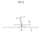
- FIG. 3 is a view for explaining an exposure operation using the above exposure system. Note that the struts of the stencil mask are not shown in FIG. 3 is.
- Electron beam EB passing through an aperture of the stencil mask SM exposes a not shown resist on a wafer W.
- the exposure system shown in FIG. 1 employs equal magnification exposure, so the stencil mask SM and the wafer W are arranged in proximity.
- control unit 10 controls the main deflectors 5 and 6 to scan the stencil mask SM by the electron beam EB so as to transfer patterns of the stencil mask to the wafer W. Further, the control unit 10 outputs a signal for controlling the deflection angle of electron beam to the sub-deflectors 7 and 8.
- the subdeflector 7 and 8 tilt the direction of the electron beam EB slightly to a normal V of the mask. Due to this, a transfer pattern is transferred displaced in position (distorted) so as to overlap an underlying pattern WP warped from its accurate position on the wafer W.
- "correction of distortion” means forming a transfer pattern distorted to match the distortion of its underlying pattern.
- FIG. 4A is a view for explaining characteristics of electron beam sub-deflection correction.
- the changes in position of a transfer pattern due to a electron beam sub-deflection function were examined in detail.
- G(x) is the offset of the transfer pattern with reference to the mask pattern after exposure (distortion of transfer pattern).
- the distortion "G" of the transfer pattern after electron beam sub-deflection correction can be considered the distortion obtained by applying a Fourier transform E of the electron beam intensity distribution K(x) as a filter to the distortion g of the underlying pattern.
- FIG. 4B is a view showing the value E obtained after a Fourier transform of the electron beam intensity distribution K(x).
- the value E indicates the correction efficiency for each frequency of distortion when correcting distortion of an underlying pattern.
- the "f" of the abscissa corresponds to the spatial frequency of the distortion of the underlying pattern.
- FIG. 4B shows an example in the case of calculation assuming the electron beam intensity distribution K(x) is a Gaussian distribution of a full width at half maximum of 500 ⁇ m.
- the value E of the Fourier transform of the electron beam intensity distribution K(x) can be used as a low pass filter.
- the EB diameter is difficult to make smaller.
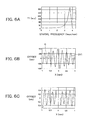
- FIGS. 5A, 5B, and 5C are graphs for explaining an example of occurrence of residual distortion in the case of correcting drastic distortion of an underlying pattern by electron beam sub-deflection correction of the related art.
- FIG. 5A shows an example of the intensity distribution of the electron beam used
- FIG. 5B shows distortion (offset) of an underlying pattern near a chip boundary (corresponding to a strut in a mask)
- FIG. 5C shows the residual distortion after transfer by sub-deflection correction.
- the electron beam intensity follows a Gaussian distribution and assumed that an electron beam having a full width at half maximum of 350 ⁇ m is used. Further, the case of using this electron beam to correct offset (distortion) of ⁇ 10 nm at chips adjoining each other across a distance of 250 ⁇ m as shown in FIG. 5B is assumed.
- the present embodiment generates a compensation signal to be output to the sub deflectors 7 and 8 for correcting an underlying pattern WP on the wafer as follows.
- the "electron beam deflection signal” is a signal of the EB deflection angle in the case of setting a target position so that the center of the electron beam overlays a distorted underlying pattern.
- the compensation filter T is a reciprocal of the value E at each frequency and increases as the frequency becomes higher. That is, it is a high pass filter. Therefore, it emphasizes offset compensation of a transfer pattern.
- the compensation filter T diverges exponentially, so even at a high frequency where it becomes so small that the Fourier transform F(g) of the distortion g of an underlying pattern can be neglected, the value obtained by applying the compensation filter T to F(g) diverges. Therefore, the filtered signal TF(g) also diverges.
- FIG. 6B is a graph of the electron beam correction target position CV1 based on a compensation signal generated by application of the compensation filter T1
- FIG. 6C is a graph of residual distortion comprised of the difference between the transfer pattern and the underlying pattern after correction. Note that "Wb" is 250 ⁇ m as an example.
- the electron beam correction target position CV1 is the position of irradiation targeted by the electron beam sub-deflection performance and corresponds to the compensation signal.
- the compensation signal is generated and output by the control unit 10. Further, FIG. 6B also shows the distortion G of an actual transfer pattern exposed by the electron beam correction target position CV1.
- FIG. 6B shows that by swinging back and forth the electron beam targeting the electron beam correction target position CV1, the latent images are overlaid and as a result finally the transfer pattern shown by G is obtained.
- the swing of the electron beam is too much larger than the pattern to be resolved, so it is impossible to overlap the images to obtain a transfer pattern in practice. Therefore, the problem arises that resolution of the transfer pattern cannot be obtained.
- FIG. 7B is a graph of an electron beam correction target position CV2 based on a compensation signal generated by applying the compensation filter T2
- FIG. 7C is a graph of the residual distortion comprised of the difference between the transfer pattern and the underlying pattern after correction. Note that "Wb" is 250 ⁇ m as an example.
- the cutoff frequency of the compensation filter T may be adjusted to select the optimal conditions. From the above, the cutoff frequency ft of the compensation filter T has to be larger than "fb". However, if too large, the electron beam correction target position will diverge and the resolution will drop.
- the most suitable range of the cutoff frequency is as shown in the following equation: fb ⁇ ft ⁇ ln( ⁇ / ⁇ )fb
- a compensation filter for canceling out the low pass filter effect of the electron beam intensity distribution (high pass filter) is generated using a Fourier transform.
- the compensation filter is applied to the electron beam deflection signal to generate a compensation signal.
- the compensation signal obtained by the above, as shown in FIG. 7B, makes the electron beam swing back and forth so as to periodically repeat forward direction correction and reverse direction correction for the distortion g of the underlying pattern.
- "Forward direction correction” means to make a position over the offset of the underlying pattern the electron beam target position
- "reverse direction correction” means to make a position not reaching the offset of the underlying pattern the electron beam target position.
- the sub deflectors 7 and 8 deflect the electron beam so as to control the incidence angle of the electron beam to the mask.
- the latent images of the forward direction correction and the latent images of the reverse direction correction can be overlaid to obtain the desired transfer pattern.
- the forward direction correction and the reverse direction correction are preferably repeated by a period and amplitude so that overlay of latent images of forward direction correction and latent images of reverse direction correction gives the resolution of the transfer pattern.
- the cutoff frequency of the compensation filter T is adjusted.
- a transfer pattern having distortion matching with a high precision the distortion of the underlayer pattern of the wafer can be obtained and the overlay accuracy of the underlying pattern and the transfer pattern can be improved. For example, if the full width at half maximum of the electron beam is 350 ⁇ m and the strut width is 250 ⁇ m, the residual distortion can be reduced to around 1 nm.
- the EB diameter of the electron beam used is preferably made the same or smaller than the strut width.
- the patterns of a semiconductor device produced by using the exposure system and the exposure method according to the present embodiment are characterized in that offsets of the transfer patterns shown by G in FIG. 7B become periodic.
- the compensation signal for correcting distortion of an underlying pattern was obtained by using a Fourier transform.
- a wavelet transform is used.
- the distortion G of a corrected transfer pattern is expressed by a convolution of the distortion g of the correction target and the electron beam intensity distribution K.
- the order "m” is the number of data points when sampling by a frequency not less than 2f max where the maximum frequency of the Fourier spectrum of the electron beam intensity distribution is "f max ". At that time, it is guaranteed that the electron beam intensity distribution can be accurately reproduced by a sampling theorem.
- "f max " is the frequency where the magnitude of the spectrum becomes small enough to be ignored.
- the system matrix is a matrix for expressing convolution of equation (1) by a matrix equation.
- W m and W n are wavelet transform matrixes.
- Haar basis or other orthogonal basis can be used.
- W m T expresses a transpose matrix of "W m " and is an inverse matrix "W m ".
- a wavelet transform by nature results in data of the system matrix M being converged near the mother wavelet (M 1,1 ) expressing the average information of the data. Therefore, by extracting a square matrix near the mother wavelet of "Mw" after the wavelet transform of the system matrix M, obtaining its inverse matrix, and applying an inverse wavelet transform, an approximate solution vector v" can be obtained.
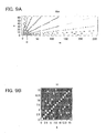
- FIG. 8A is a graph of distortion near chip boundaries for calculation of distortion compensation and shows a case of offset of ⁇ 10 nm at chips adjoining each other across a space of 240 nm.
- the distortion of the underlying pattern shown in FIG. 8A corresponds to the "q" in equation (4), while the position on the abscissa in FIG. 8B corresponds to the order "n".
- FIG. 8B is shows the electron beam intensity distribution K as well.
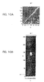
- FIG. 9A is a contour graph of the matrix M w obtained by applying a two-dimensional wavelet transform to the system matrix M shown in FIG. 8B.
- the Haar basis is an orthogonal basis, so can transform data completely similar to a Fourier transform.
- FIG. 9B is a view obtained by extracting a 16 x 16 partial matrix H shown by the square frame in FIG. 9A and expresses the magnitudes of the elements of the partial matrix H by shading.
- FIG. 10A is a graph obtained by finding an inverse matrix H -1 of the partial matrix H shown in FIG. 9B and expressing the magnitudes of the elements of the inverse matrix H -1 by shading.
- the 16 x 16 inverse matrix H -1 is given an 0 element at its outside to make the 256 x 64 matrix shown in FIG. 10B and thereby generate an approximate inverse matrix H' -1 of M w .
- Equation (11) the approximate inverse matrix M inv of the system matrix M is expressed by the following equation (11).
- Equation (12) "M inv " is given by a two-dimensional wavelet transform of "H' -1 ".
- M inv W m T ⁇ H' -1 ⁇ W n
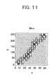
- FIG. 11 is a graph expressing the magnitudes of the elements of the approximate inverse matrix M inv shown in equation (11) by shading.
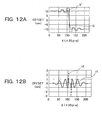
- FIG. 12A is a graph of the distortion G of a transfer pattern predicted at the time of electron beam sub-deflection correction using the compensation signal v" given by equation (12).
- “r1” is the residual distortion after electron beam sub-deflection correction according to the present embodiment
- “r2" is the residual distortion after electron beam sub-deflection correction of the related art.
- a residual distortion of 3 nm occurs at the chip boundaries in the related art, but the residual distortion can be suppressed to ⁇ 1 nm in the electron beam scan method according to the present embodiment. Therefore, the overlay accuracy between the underlying pattern and the transfer pattern can be improved.
- the correction target position v" and the residual distortion do not diverge at the two ends of a calculation area. That is, with the method of generating a compensation signal using a wavelet transform, the signal converges at positions away from the drastic distortion, so is suited for actual electron beam sub-deflection correction.
- the compensation signal generated using the Fourier transform explained in the first embodiment covers not only the vicinity the drastic distortion, but also the entire region.
- the compensation signal generated using a wavelet transform is localized at only drastic distortion. That is, a Fourier transform transforms all positional coordinates to frequency, so positional data is lost.
- a wavelet transform transforms spanning both position and frequency, so no positional data is lost.
- a transfer pattern matching with a high precision the distortion of the underlying pattern of an exposed member can be obtained, and the overlay accuracy between the underlying pattern and the transfer pattern can be improved.
- the present invention is not limited to the method such as the first embodiment in which a compensation filter prepared using a Fourier transform is applied to the electron beam deflection signal to obtain a compensation signal or the method such as the second embodiment in which wavelet transform is used to obtain a compensation signal suitable for control.
- it is not particularly limited so long as a transfer pattern reduced in distortion due to repeated forward direction correction and reverse direction correction and overlay of latent images can be obtained.
- the EB diameter of the electron beam is not limited.
- any charged particle beam other than an electron beam, such as ion beam can also be used.
Abstract
Description
Claims (11)
- An exposure system comprising:a mask arranged at a position facing to an exposed member having an underlying pattern and formed with a pattern to be transferred to the exposed member,a charged particle beam scanning means for scanning the mask by a charged particle beam, andan incidence angle controlling means for controlling an incidence angle of the charged particle beam to the mask so as to make forward direction correction and reverse direction correction of the position of the transfer pattern with respect to distortion of the underlying pattern.
- An exposure system as set forth in claim 1, wherein said incidence angle controlling means controls the incidence angle of said charged particle beam to said mask so as to repeat said forward direction correction and said reverse direction correction at a frequency and amplitude able to obtained resolution of said transfer pattern.
- An exposure system as set forth in claim 1, wherein
said mask has struts forming areas where said exposed member is not exposed, and
said charged particle beam scanning means scans said mask by a charged particle beam having a diameter smaller not more than a width of said struts. - An exposure system as set forth in claim 1, wherein said incidence angle controlling means controls the incidence angle of said charged particle beam to said mask for distortion of an underlying pattern occurring at an area smaller than the diameter of said charged particle beam.
- An exposure system as set forth in claim 1, wherein said incidence angle controlling means comprises:a compensation signal generating means for applying a compensation filter to a deflection signal for correcting distortion of said underlying pattern as it is to generate a compensation signal, said compensation filter corresponding to a reciprocal of the value found by applying a Fourier transform to an electron beam intensity distribution anda deflecting means for deflecting said charged particle beam according to said generated compensation signal to control said incidence angle.
- An exposure system as set forth in claim 5, wherein said compensation signal generating means applies said compensation filter cut off in a finite frequency area to said deflection signal to generate said compensation signal so as to suppress divergence of said compensation signal.
- An exposure system as set forth in claim 1, wherein said incidence angle controlling means comprises:a compensation signal generating means for generating a compensation signal based on an approximate inverse matrix of a system matrix and distortion of said underlying pattern, said approximate inverse matrix based on a low frequency component extracted by a wavelet transform of said system matrix expressed using electron beam intensity distribution, anda deflecting means for deflecting said charged particle beam according to said generated compensation signal to control said incidence angle.
- An exposure method for arranging a mask facing an exposed member having an underlying pattern and forming a transfer pattern on the exposed member by a charged particle beam passing an aperture pattern formed in the mask, comprising a step of scanning the mask by the charged particle beam controlled an incidence angle of that to the mask so as to make forward direction correction and reverse direction correction of the position of the transfer pattern and forming the transfer pattern at the exposed member.
- An exposure method as set forth in claim 8, wherein the incidence angle of said charged particle beam to said mask is controlled so as to repeat said forward direction correction and said reverse direction correction at a frequency and amplitude able to obtain resolution of said transfer pattern.
- An exposure method as set forth in claim 8, wherein said mask has struts where said exposed member is not exposed and is scanned by said charged particle beam having a diameter not more than a width of said struts.
- An exposure method as set forth in claim 8, wherein said incidence angle of said charged particle beam to said mask is controlled so as to make forward direction correction and reverse direction correction to distortion of said underlying pattern occurring at an area smaller than the diameter of said charged particle beam.
Applications Claiming Priority (4)
| Application Number | Priority Date | Filing Date | Title |
|---|---|---|---|
| JP2003194460 | 2003-07-09 | ||
| JP2003194460 | 2003-07-09 | ||
| JP2004020202 | 2004-01-28 | ||
| JP2004020202A JP2005045200A (en) | 2003-07-09 | 2004-01-28 | Exposure system and exposure method |
Publications (2)
| Publication Number | Publication Date |
|---|---|
| EP1496540A2 true EP1496540A2 (en) | 2005-01-12 |
| EP1496540A3 EP1496540A3 (en) | 2007-01-17 |
Family
ID=33455614
Family Applications (1)
| Application Number | Title | Priority Date | Filing Date |
|---|---|---|---|
| EP04016126A Withdrawn EP1496540A3 (en) | 2003-07-09 | 2004-07-08 | Exposure system and exposure method |
Country Status (5)
| Country | Link |
|---|---|
| US (1) | US6974960B2 (en) |
| EP (1) | EP1496540A3 (en) |
| JP (1) | JP2005045200A (en) |
| KR (1) | KR20050007167A (en) |
| TW (1) | TWI268404B (en) |
Families Citing this family (4)
| Publication number | Priority date | Publication date | Assignee | Title |
|---|---|---|---|---|
| JP4945763B2 (en) * | 2005-05-17 | 2012-06-06 | 国立大学法人京都大学 | Electron beam exposure system |
| US20150146179A1 (en) * | 2013-11-25 | 2015-05-28 | Takao Utsumi | Low energy electron beam lithography |
| JP6027150B2 (en) | 2014-06-24 | 2016-11-16 | 内海 孝雄 | Low energy electron beam lithography |
| CN113594076B (en) * | 2021-07-22 | 2023-06-20 | 上海精测半导体技术有限公司 | Alignment method of patterned wafer and semiconductor device |
Citations (3)
| Publication number | Priority date | Publication date | Assignee | Title |
|---|---|---|---|---|
| US5831272A (en) * | 1997-10-21 | 1998-11-03 | Utsumi; Takao | Low energy electron beam lithography |
| US20020096646A1 (en) * | 2001-01-22 | 2002-07-25 | Nobuo Shimazu | Electron beam proximity exposure apparatus and method |
| US20040086790A1 (en) * | 2001-06-08 | 2004-05-06 | Shigeru Moriya | Mask, method of producing mask, and method of producing semiconductor device |
Family Cites Families (1)
| Publication number | Priority date | Publication date | Assignee | Title |
|---|---|---|---|---|
| US6717157B2 (en) * | 2002-07-03 | 2004-04-06 | Leepl Corporation | Mask inspecting apparatus |
-
2004
- 2004-01-28 JP JP2004020202A patent/JP2005045200A/en active Pending
- 2004-07-08 TW TW093120516A patent/TWI268404B/en not_active IP Right Cessation
- 2004-07-08 EP EP04016126A patent/EP1496540A3/en not_active Withdrawn
- 2004-07-09 KR KR1020040053237A patent/KR20050007167A/en not_active Application Discontinuation
- 2004-07-09 US US10/888,468 patent/US6974960B2/en not_active Expired - Fee Related
Patent Citations (3)
| Publication number | Priority date | Publication date | Assignee | Title |
|---|---|---|---|---|
| US5831272A (en) * | 1997-10-21 | 1998-11-03 | Utsumi; Takao | Low energy electron beam lithography |
| US20020096646A1 (en) * | 2001-01-22 | 2002-07-25 | Nobuo Shimazu | Electron beam proximity exposure apparatus and method |
| US20040086790A1 (en) * | 2001-06-08 | 2004-05-06 | Shigeru Moriya | Mask, method of producing mask, and method of producing semiconductor device |
Also Published As
| Publication number | Publication date |
|---|---|
| KR20050007167A (en) | 2005-01-17 |
| TWI268404B (en) | 2006-12-11 |
| JP2005045200A (en) | 2005-02-17 |
| US20050116185A1 (en) | 2005-06-02 |
| TW200513804A (en) | 2005-04-16 |
| EP1496540A3 (en) | 2007-01-17 |
| US6974960B2 (en) | 2005-12-13 |
Similar Documents
| Publication | Publication Date | Title |
|---|---|---|
| US6433348B1 (en) | Lithography using multiple pass raster-shaped beam | |
| JP5090887B2 (en) | Drawing method for electron beam drawing apparatus and electron beam drawing apparatus | |
| JP5549032B2 (en) | Method for forming a pattern on a target surface by a charged particle beam | |
| JP2010041055A (en) | Correction of irradiation nonuniformity and image distortion | |
| US6940080B2 (en) | Charged particle beam lithography system, lithography method using charged particle beam, method of controlling charged particle beam, and method of manufacturing semiconductor device | |
| US10497539B2 (en) | Multi charged particle beam writing apparatus and multi charged particle beam writing method | |
| KR20100103650A (en) | Electron beam exposure system | |
| JP2842737B2 (en) | Electron beam exposure method | |
| JPH10214779A (en) | Electron beam exposure method and fabrication of device using that method | |
| US20130288181A1 (en) | Drawing apparatus, and method of manufacturing article | |
| TW202001968A (en) | Data processing method, data processing apparatus, and multiple charged-particle beam writing apparatus | |
| KR102498820B1 (en) | Optical alignment correction using convolutional neural network evaluation of a beam image | |
| JP2006186125A (en) | Charged particle beam exposure device and its exposure method | |
| JP4207232B2 (en) | Charged beam exposure system | |
| JP2007329220A (en) | Multiple beam charged particle beam apparatus and method of controlling the same, and method of manufacturing device | |
| US6974960B2 (en) | Exposure system and exposure method | |
| US7005659B2 (en) | Charged particle beam exposure apparatus, charged particle beam exposure method, and device manufacturing method using the same apparatus | |
| JP2002289517A (en) | Electron beam proximity exposure system and method | |
| KR20180088600A (en) | Advanced doselevel quantization for multibeam-writers | |
| US20050036175A1 (en) | Optical proximity correction in raster scan printing based on grayscale manipulation of the bitmap | |
| KR101988911B1 (en) | Multi-charged particle beam writing apparatus and adjusting method thereof | |
| US9846760B2 (en) | Writing data verification method and multi-charged particle beam writing apparatus | |
| JP3080006B2 (en) | Electron beam exposure correction method | |
| JP2005129850A (en) | Charged beam drawing apparatus and method | |
| JP2003332206A (en) | Aligner using electron beam and processing device using the electronic beam |
Legal Events
| Date | Code | Title | Description |
|---|---|---|---|
| PUAI | Public reference made under article 153(3) epc to a published international application that has entered the european phase |
Free format text: ORIGINAL CODE: 0009012 |
|
| AK | Designated contracting states |
Kind code of ref document: A2 Designated state(s): AT BE BG CH CY CZ DE DK EE ES FI FR GB GR HU IE IT LI LU MC NL PL PT RO SE SI SK TR |
|
| AX | Request for extension of the european patent |
Extension state: AL HR LT LV MK |
|
| PUAL | Search report despatched |
Free format text: ORIGINAL CODE: 0009013 |
|
| AK | Designated contracting states |
Kind code of ref document: A3 Designated state(s): AT BE BG CH CY CZ DE DK EE ES FI FR GB GR HU IE IT LI LU MC NL PL PT RO SE SI SK TR |
|
| AX | Request for extension of the european patent |
Extension state: AL HR LT LV MK |
|
| 17P | Request for examination filed |
Effective date: 20070702 |
|
| AKX | Designation fees paid |
Designated state(s): DE FR |
|
| 17Q | First examination report despatched |
Effective date: 20071227 |
|
| STAA | Information on the status of an ep patent application or granted ep patent |
Free format text: STATUS: THE APPLICATION IS DEEMED TO BE WITHDRAWN |
|
| 18D | Application deemed to be withdrawn |
Effective date: 20120201 |