EP1501115B1 - Dual beam system - Google Patents
Dual beam system Download PDFInfo
- Publication number
- EP1501115B1 EP1501115B1 EP04076891A EP04076891A EP1501115B1 EP 1501115 B1 EP1501115 B1 EP 1501115B1 EP 04076891 A EP04076891 A EP 04076891A EP 04076891 A EP04076891 A EP 04076891A EP 1501115 B1 EP1501115 B1 EP 1501115B1
- Authority
- EP
- European Patent Office
- Prior art keywords
- work piece
- magnetic field
- electron
- beam column
- objective lens
- Prior art date
- Legal status (The legal status is an assumption and is not a legal conclusion. Google has not performed a legal analysis and makes no representation as to the accuracy of the status listed.)
- Active
Links
- 230000009977 dual effect Effects 0.000 title claims description 20
- 238000010884 ion-beam technique Methods 0.000 claims description 43
- 239000011163 secondary particle Substances 0.000 claims description 29
- 238000010894 electron beam technology Methods 0.000 claims description 24
- 150000002500 ions Chemical class 0.000 claims description 13
- 238000000034 method Methods 0.000 claims description 13
- 230000003472 neutralizing effect Effects 0.000 claims description 11
- 239000000696 magnetic material Substances 0.000 claims description 2
- 229910052733 gallium Inorganic materials 0.000 description 24
- GYHNNYVSQQEPJS-UHFFFAOYSA-N Gallium Chemical compound [Ga] GYHNNYVSQQEPJS-UHFFFAOYSA-N 0.000 description 18
- 239000002245 particle Substances 0.000 description 17
- 230000008859 change Effects 0.000 description 12
- 238000004088 simulation Methods 0.000 description 8
- 230000005591 charge neutralization Effects 0.000 description 7
- -1 gallium ions Chemical class 0.000 description 6
- 238000004519 manufacturing process Methods 0.000 description 6
- 230000013011 mating Effects 0.000 description 6
- 230000003287 optical effect Effects 0.000 description 6
- 239000000203 mixture Substances 0.000 description 5
- 238000003032 molecular docking Methods 0.000 description 5
- 230000000694 effects Effects 0.000 description 4
- 230000000155 isotopic effect Effects 0.000 description 4
- 230000007246 mechanism Effects 0.000 description 4
- 230000008569 process Effects 0.000 description 4
- 239000000758 substrate Substances 0.000 description 4
- 230000002411 adverse Effects 0.000 description 3
- 229910001338 liquidmetal Inorganic materials 0.000 description 3
- 230000000979 retarding effect Effects 0.000 description 3
- 230000004075 alteration Effects 0.000 description 2
- 238000002347 injection Methods 0.000 description 2
- 239000007924 injection Substances 0.000 description 2
- 239000000463 material Substances 0.000 description 2
- 239000000243 solution Substances 0.000 description 2
- 125000003821 2-(trimethylsilyl)ethoxymethyl group Chemical group [H]C([H])([H])[Si](C([H])([H])[H])(C([H])([H])[H])C([H])([H])C(OC([H])([H])[*])([H])[H] 0.000 description 1
- XUIMIQQOPSSXEZ-UHFFFAOYSA-N Silicon Chemical compound [Si] XUIMIQQOPSSXEZ-UHFFFAOYSA-N 0.000 description 1
- 230000009471 action Effects 0.000 description 1
- 230000005540 biological transmission Effects 0.000 description 1
- 238000010276 construction Methods 0.000 description 1
- 239000000498 cooling water Substances 0.000 description 1
- 230000001934 delay Effects 0.000 description 1
- 238000010586 diagram Methods 0.000 description 1
- 230000005684 electric field Effects 0.000 description 1
- 230000005686 electrostatic field Effects 0.000 description 1
- 238000010304 firing Methods 0.000 description 1
- CKHJYUSOUQDYEN-UHFFFAOYSA-N gallium(3+) Chemical compound [Ga+3] CKHJYUSOUQDYEN-UHFFFAOYSA-N 0.000 description 1
- 230000020169 heat generation Effects 0.000 description 1
- 238000007689 inspection Methods 0.000 description 1
- 239000011810 insulating material Substances 0.000 description 1
- 238000002955 isolation Methods 0.000 description 1
- 230000005415 magnetization Effects 0.000 description 1
- 238000005459 micromachining Methods 0.000 description 1
- 229910000595 mu-metal Inorganic materials 0.000 description 1
- 238000000206 photolithography Methods 0.000 description 1
- 239000010453 quartz Substances 0.000 description 1
- 230000008439 repair process Effects 0.000 description 1
- 238000004626 scanning electron microscopy Methods 0.000 description 1
- 239000004065 semiconductor Substances 0.000 description 1
- 229910052710 silicon Inorganic materials 0.000 description 1
- 239000010703 silicon Substances 0.000 description 1
- VYPSYNLAJGMNEJ-UHFFFAOYSA-N silicon dioxide Inorganic materials O=[Si]=O VYPSYNLAJGMNEJ-UHFFFAOYSA-N 0.000 description 1
- 238000006467 substitution reaction Methods 0.000 description 1
- WFKWXMTUELFFGS-UHFFFAOYSA-N tungsten Chemical compound [W] WFKWXMTUELFFGS-UHFFFAOYSA-N 0.000 description 1
Images


Classifications
-
- H—ELECTRICITY
- H01—ELECTRIC ELEMENTS
- H01J—ELECTRIC DISCHARGE TUBES OR DISCHARGE LAMPS
- H01J37/00—Discharge tubes with provision for introducing objects or material to be exposed to the discharge, e.g. for the purpose of examination or processing thereof
- H01J37/02—Details
- H01J37/04—Arrangements of electrodes and associated parts for generating or controlling the discharge, e.g. electron-optical arrangement, ion-optical arrangement
- H01J37/10—Lenses
- H01J37/14—Lenses magnetic
- H01J37/141—Electromagnetic lenses
-
- H—ELECTRICITY
- H01—ELECTRIC ELEMENTS
- H01J—ELECTRIC DISCHARGE TUBES OR DISCHARGE LAMPS
- H01J37/00—Discharge tubes with provision for introducing objects or material to be exposed to the discharge, e.g. for the purpose of examination or processing thereof
- H01J37/02—Details
- H01J37/026—Means for avoiding or neutralising unwanted electrical charges on tube components
-
- H—ELECTRICITY
- H01—ELECTRIC ELEMENTS
- H01J—ELECTRIC DISCHARGE TUBES OR DISCHARGE LAMPS
- H01J37/00—Discharge tubes with provision for introducing objects or material to be exposed to the discharge, e.g. for the purpose of examination or processing thereof
- H01J37/02—Details
- H01J37/04—Arrangements of electrodes and associated parts for generating or controlling the discharge, e.g. electron-optical arrangement, ion-optical arrangement
- H01J37/08—Ion sources; Ion guns
-
- H—ELECTRICITY
- H01—ELECTRIC ELEMENTS
- H01J—ELECTRIC DISCHARGE TUBES OR DISCHARGE LAMPS
- H01J2237/00—Discharge tubes exposing object to beam, e.g. for analysis treatment, etching, imaging
- H01J2237/004—Charge control of objects or beams
- H01J2237/0041—Neutralising arrangements
- H01J2237/0042—Deflection of neutralising particles
-
- H—ELECTRICITY
- H01—ELECTRIC ELEMENTS
- H01J—ELECTRIC DISCHARGE TUBES OR DISCHARGE LAMPS
- H01J2237/00—Discharge tubes exposing object to beam, e.g. for analysis treatment, etching, imaging
- H01J2237/06—Sources
- H01J2237/08—Ion sources
- H01J2237/0802—Field ionization sources
- H01J2237/0805—Liquid metal sources
-
- H—ELECTRICITY
- H01—ELECTRIC ELEMENTS
- H01J—ELECTRIC DISCHARGE TUBES OR DISCHARGE LAMPS
- H01J2237/00—Discharge tubes exposing object to beam, e.g. for analysis treatment, etching, imaging
- H01J2237/10—Lenses
- H01J2237/14—Lenses magnetic
- H01J2237/1405—Constructional details
-
- H—ELECTRICITY
- H01—ELECTRIC ELEMENTS
- H01J—ELECTRIC DISCHARGE TUBES OR DISCHARGE LAMPS
- H01J2237/00—Discharge tubes exposing object to beam, e.g. for analysis treatment, etching, imaging
- H01J2237/26—Electron or ion microscopes
- H01J2237/28—Scanning microscopes
-
- H—ELECTRICITY
- H01—ELECTRIC ELEMENTS
- H01J—ELECTRIC DISCHARGE TUBES OR DISCHARGE LAMPS
- H01J2237/00—Discharge tubes exposing object to beam, e.g. for analysis treatment, etching, imaging
- H01J2237/30—Electron or ion beam tubes for processing objects
- H01J2237/317—Processing objects on a microscale
- H01J2237/31749—Focused ion beam
Landscapes
- Chemical & Material Sciences (AREA)
- Analytical Chemistry (AREA)
- Physics & Mathematics (AREA)
- Electromagnetism (AREA)
- Electron Sources, Ion Sources (AREA)
- Analysing Materials By The Use Of Radiation (AREA)
Description
- The present invention relates to charged particle beam systems, and in particular to systems including an ion beam column and an electron beam column using a magnetic objective lens.
- Charged particle beam systems are used in a variety of applications, including the manufacturing, repair, and inspection of miniature devices, such as integrated circuits, magnetic recording heads, and photolithography masks. Dual beam systems often include a scanning electron microscope (SEM) that can provide a high-resolution image with minimal damage to the target, and an ion beam system, such as a focused or shaped beam system, that can be used to alter substrates and to form images.
- One common application for a dual beam system is to expose a buried portion of a substrate and then to form an image of the exposed surface. For example, a focused or shaped ion beam can be used to make a vertical cut in a substrate to expose a cross sectional surface, and then an electron beam can be scanned over the newly exposed surface to form an image of it.
- One difficulty with such systems is that the final lens of the scanning electron microscope produces a magnetic field, which alters the trajectory of the ion beam and also interferes with various other functions of the dual beam system. For example, an image or information about the composition of the substrate can be obtained by collecting secondary particles ejected as the primary ion beam strikes target. The magnetic field of the SEM, however, changes the path of the secondary particles and makes them difficult to collect.
- When a work piece in a charged particle beam system is composed of an insulating material, such as quartz, the work piece tends to accumulate electrical charge that adversely affects the primary beams and secondary particles. One method of neutralizing the change entails the use of an electron flood gun that directs electrons to the work piece to neutralize positive charge. An electron flood gun differs from an electron microscope in that the flood gun lack precise optics options and produces a relatively broad beam of low energy electrons. The magnetic field of the SEM changes the path of the neutralizing electrons from the flood gun and makes it difficult to direct them accurately toward the work piece.
- A common solution to this problem of the magnetic field interference is to turn off the SEM when using the ion beam or when using certain functions of the ion beam system. For example, the SEM can be switched off to allow collection of the ion beam induced secondary particles or when using a charge neutralization flood gun. Turning the SEM lens on and off creates its own set of problems.
- The magnetic objective lens of an SEM uses a significant electrical current and therefore generates a significant amount of heat, the heat being proportional to the square of the current. The heat dissipated by an SEM causes components of the dual beam system to expand. The resolution of an SEM, being on the order of magnitude of nanometers requires a very stable physical platform, and the system therefore requires a significant amount of time after being turned on to reach thermal equilibrium and become stable. As the resolution of systems has increased, stability has become more important, and longer waits are required. Charged particle beam systems were originally used only in laboratories to analyze samples, and the time to reach thermal equilibrium was acceptable. Systems are now being used as production equipment and such delays are unacceptable.
-
U.S. Pat. No. 4,345,152 for a "Magnetic Lens" describes an electron lens that uses two coils having equal numbers of turns wound in opposite directions. By altering the allocation of current between the two coils, the magnetic field could be adjusted to focus the electron beam while maintaining a constant total current, and therefore a constant heat output. Using two lenses of equal turns allows the magnetic field to be varied or even cancelled without changing the total electrical current in the lens. Thus, the magnetic field could be eliminated without changing the heat output of the lens. - The surface viewed by the SEM is often oriented at a non-perpendicular angle to the SEM axis, so one part of the work piece is closer to the lens than another part. To compensate for the difference in distance, some SEMs change the focus of the objective lens during the scan and can therefore produce a clearer image. This is often referred to as "dynamic focusing." Dynamic focusing requires the ability to rapidly change the magnetic field, which requires rapidly changing the electrical current in the objective lens coils. The coil inductance, which is related to the number of turns of the coil, resists a current change.
- The two equal coils in
U.S. Pat. No. 4,345,152 have high inductance and cannot be changed rapidly. It is also known to use a separate, small lens for dynamic focusing. Such lenses have low inductance, but changing the lens current changes the power dissipation of the lens, which can upset the thermal equilibrium of the system, thereby reducing resolution. - If one designed a dual beam system to compensate for the effects of a constant magnetic field from the SEM objective lens, the problem would not be solved completely, because the magnetic field is not constant. To keep the SEM in focus, the magnetic field of the objective lens is changed depending upon the height of the work piece, the magnification, and the electron energy. In some system, it is possible to reduce the operating variation in the magnetic field by using "retarding field optics," that is, changing the voltage of the work piece to change the focus of the electron beam, rather than changing the magnetic field in the objective lens. In many dual beam systems, the FIB is mounted vertically and the SEM is mounted at an angle to view to vertical cross section cut by the FIB. A system in which the SEM is tilted cannot easily use retarding field options, since the tilt eliminates the symmetry of the retarding electric field and causes undesirable aberrations in the primary electron beam and difficulty in the collection of secondary electrons.
- An object of the invention is to provide a dual beam system in which an ion beam can operate while the SEM lens has current flowing in it.
- One aspect of the invention comprises a dual beam system in which the objective lens of an SEM can be energized while other functions of the system can still be used. The SEM produces a constant heat generation so that the system does not need extra time to reach thermal equilibrium when the magnetic field strength is changed to focus the beam. A charge neutralization flood gun is positioned so that the magnetic field helps to direct the neutralizing electrons to the target and steering electrodes in the flood gun alter the beam direction to compensate for changes in the magnetic field.
- Some embodiments include a secondary particle detector that is positioned such that the magnetic field of the SEM lens helps in the collection of secondary particles. Another embodiment uses monoisotopic gallium that eliminates blurring of the ion beam caused by the different effects of the SEM magnetic field with the different isotopes of gallium.
- The foregoing has outlined rather broadly the features and technical advantages of the present invention in order that the detailed description of the invention that follows may be better understood. Additional features and advantages of the invention will be described hereinafter. It should be appreciated by those skilled in the art that the conception and specific embodiment disclosed may be readily utilized as a basis for modifying or designing other structures for carrying out the same purposes of the present invention. It should also be realized by those skilled in the art that such equivalent constructions do not depart from the spirit and scope of the invention as set forth in the appended claims.
- For a more thorough understanding of the present invention, and the advantages thereof, reference is now made to the following descriptions taken in conjunction with the accompanying drawings, in which:
-
FIG. 1 shows part of a dual beam system embodying aspects of the invention -
FIG. 2 shows a bottom perspective view of the part of the system shown inFIG. 1 . -
FIG. 3 shows the desired trajectories of neutralizing electrodes in a magnetic field. -
FIG. 4 shows an electron flood gun that can be used with the system ofFIG. 1 . -
FIG. 5 shows an electron optical element used in the flood gun ofFIG. 4 -
FIG. 6 shows a bottom view of the system ofFIG. 1 . -
FIG. 7 shows a cross sectional view of a portion of the system ofFIG. 1 . -
FIG. 8 is a simulation showing the trajectories of ion beam induced secondary electrons in the presence of a magnetic field. -
FIG. 9 shows the desired trajectories of secondary electrons in the presence of magnetic field. -
FIG. 10 is a simulation showing the preferred trajectories of secondary charged particles in the presence of magnetic field. -
FIG. 11 shows a preferred scanning electron microscope column used in the system ofFIG. 1 . -
FIG. 12 shows the trajectories of gallium ions in a focused ion beam using a source composed of naturally occurring gallium. -
FIG. 13A is a focused ion beam image formed using a beam of dual isotopic gallium in the presence of the minimum magnetic field produced by the magnetic objective lens of a nearby scanning electron microscopic.FIG. 13B is a focused ion beam image formed using a beam of dual isotopic gallium in the presence of the maximum magnetic field produced by the magnetic objective lens of a nearby scanning electron microscopic. -
FIG. 14 shows the trajectories of gallium ions in a focused ion beam using monoisotopic gallium. -
FIG. 15A is a focused ion beam image formed using a beam of monoisotopic gallium in the presence of the minimum magnetic field produced by the magnetic objective lens of a nearby scanning electron microscopic.FIG. 15B is a focused ion beam image formed using a beam of monoisotopic gallium in the presence of the maximum magnetic field produced by the magnetic objective lens of a nearby scanning electron microscopic. -
FIGS. 16A and 16B show a docking mechanism that can be used in the system ofFIG. 1 .FIG. 16A shows the docking mechanism in isolation mode andFIG. 16B shows the docking mechanism in docking mode. -
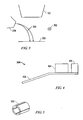
FIG. 1 shows a portion of adual beam system 96 that includes aturret 98 upon which are mounted anscanning electron microscope 100, anion beam column 102, alight microscope 105, one or more gas injection systems (GIS) 110, and anelectron detector 114 that detects electrons collected through the lens ofSEM 100 and deflected away from the primary electron beam axis.FIG. 2 shows the same component as seen from underneath, that is, as seen from the work piece surface. A chargeneutralization flood gun 204 and asecondary particle detector 205, such as a channel detector electron multiplier (CDEM) that detects particles generated from the work piece by the impact of ions fromion beam column 102, are visible inFIG. 2 . - Although the ion beam and the electron beam ideally point to the identical spot on the work piece, the physical sizes of the electron beam column and the ion beam column typically prevent them from being positioned very close to the surface and directed toward the same target spot. To have both beams pointing to the same spot, one or both beams must typically be backed away from the surface. Backing a column away from the surface increases the working distance, that is, the from the column final lens to the work piece surface. Increasing the working distance reduces the resolution of the column.
- In a preferred embodiment that provides a short working distance for both columns, the impact points from the
SEM 100 and theFIB 104 are offset from each other, for example, by about 50 mm. The work piece is mounted in a work piece holder or stage (not shown) that moves the work piece rapidly and accurately between the two spots depending upon which beam is being used. As the stage moves in the X-Y plane to position the work piece under the appropriate beam column, the stage also moves vertically to compensate for variations in the surface height of the work piece. Such surface height variations can be caused, for example, by warp in a semiconductor wafer. - A height sensor, such as a capacitive sensor 206 (
FIG. 2 ), detects a change in height of the work piece surface as the stage is moved and raises or lowers the stage so that the work piece does not collide with any of the instruments in the vacuum chamber and so that the work piece is in focus regardless of which beam is being applied to the work piece. In one embodiment, thecapacitive sensor 206 is conveniently mounted on and extends from optionaloptical microscope 105. Theoptical microscope 105 can be used for preliminary alignment of the work piece. - The various components of the system, such as
SEM 100,FIB 102, andGISs 110, are mounted onturret 98, which comprises the upper portion of a sample vacuum chamber. The turret includes various openings upon which instruments can be mounted or which can be readily sealed if not needed. By using such a turret, different charged particle beam systems can be readily configured from the same basic system. For example, different types of detectors or different numbers of gas injection systems can be mounted onto the turret to create a special or general purpose charged particle beam system, without having to design a system entirely from scratch. - The neutralizing electrons from the flood gun preferably land on the work piece at the point where the charge is accumulating, that is, near the impact point of the primary ion beam. The charge neutralizing electrons also preferably land on the work piece with a minimum of energy. In a preferred system in which the SEM objective lens is maintained in an energized state, the magnetic field from the objective lens distorts the trajectory of electrons from
flood gun 204 and can make them miss the area to be neutralized. The magnetic field from the SEM objective lens is typically around 2 mT near the ion beam impact point on the work piece. During operation of the SEM obj ective lens, the magnetic field can vary by a factor of two or more, as the strength of the lens is adjusted to maintain focus under different conditions. - The magnetic field generated by the SEM objective lens affects the neutralizing electrons not only after they leave the flood gun, but also within the flood gun as the electron beam is being produced. Although it would be possible to shield the flood gun using a material of high magnetization, referred to as a "mu-metal" material, such a magnetic shield would alter the magnetic field in the vacuum chamber and would adversely affect the focusing of the SEM. One solution is to turn off the SEM lens when using charge neutralization with the FIB beam but, as described above, turning on and off the SEM objective lens upsets the thermal equilibrium of the system and necessitates a waiting period for the system to reach thermal equilibrium.
- The invention overcomes this problem by using a two-fold approach that allows charge neutralization in the presence of the variable magnetic field of the SEM objective lens. The first aspect includes positioning and orienting the flood gun in a manner that considers the effect of the magnetic field. In other words, the flood gun is positioned and oriented so that the magnetic field accelerates the neutralizing electrons toward the target, rather than away from it.
FIG. 3 shows schematically thetrajectories 304 of the electrons fromflood gun 204 as influenced by amagnetic field 302 directed into the plane of the paper. By positioning theflood gun 204 in a preferred position and orientation, electrons from the flood gun are impact thework piece surface 306 at the correct location and at a 90 degree angle. - The second aspect of compensating for the magnetic field includes designing the flood gun for operation in a magnetic field.
FIG. 4 shows aflood gun 204 useful in connection with the invention.Flood gun 204 includes two primary sections, afiring unit 404 comprising a tungsten wire that is heated to emit electrons, and an accelerating/steering /focusingunit 406 that includes electron optical parts that accelerate, steer, and focus the electrons. Both units are supported on abracket 408 that is mounted onto the vacuum chamber. Theflood gun 204 is preferably composed of non-magnetic materials to reduce distortion of the objective lens field. -
Flood gun 204 includes steering electrodes that allow the beam of electrons to be directed. The beam is initially oriented to maximize the charge neutralization with an average magnetic field present. This orientation can be determined empirically. As the magnetic field changes on the SEM lens, the trajectories of the electrons in the neutralizing beam will change. The voltages on the steering electrodes are then adjusted to slightly steer the electrons back to the target to effect charge neutralization. The steering compensates to some extent for the deviation from ideal flood gun position and orientation. - In a preferred embodiment, the same optical components can be used to both focus and steer the electron beam. The preferred component includes a cylindrical
electrostatic lens 502 that is split into four sections as shown inFIG. 5 . A focusing voltage can be applied equally to the four elements, and a steering voltage can be superimposed on top of the focusing voltage on opposing elements. By using the same elements to steer and accelerate the beam, the electron path within the flood gun is kept short by reducing the number of components. Keeping the electron path within in the flood gun short reduces the time that the magnetic field acts on the electrons in the flood gun beam. In another embodiment, a curved flood gun can be used to compensate for the curved electron trajectory in the flood gun caused by the magnetic field. - The flood gun is also positioned such that electrons leaving the flood gun will be moved by the magnetic field toward the target, rather than away from the target. The preferred position of the flood gun varies with the specific application. The preferred position for the flood gun can be determined by performing a three dimensional simulation of the magnetic field generated by the SEM objective lens and combining that field with a three dimensional simulation of the electrostatic field within the flood gun. For example, applicants used Munro electron beam simulation software available from MEBS Ltd., London, UK to simulate the electron trajectories in the various fields. The configuration of the SEM objective gun lens is input into the MEBS program, and the program then determines the magnetic fields and calculates the trajectory of the electrons from the flood gun. The position and orientation of the flood gun in the simulation can be altered until the electrons land in the desired place.
-
FIGS. 6 and7 show the preferred orientations of theflood gun 204 and other components in one embodiment having avertical FIB column 102 and anSEM column 100 oriented at 45 degrees aimed at a spot about 50 mm from the FIB target on awork piece 600, for example, a 300 mm silicon wafer. The objective lens ofSEM column 100 is positioned about 1.4 mm from the target point.Fig. 6 shows the orientation of the various components viewed from underneath, that is, with the axis of theion beam column 102 extending into the page.FIG. 7 shows a partial cross sectional view of the system ofFIG. 6. FIG. 6 shows that theflood gun 204 is preferably positioned in a vertical plane that is ninety degrees clockwise, when viewed from below, from the vertical plane containing theSEM 100. -
FIG. 7 shows that theflood gun 204 is oriented at anangle 702 of preferably about 40 degrees from the horizontal and that the end of the flood gun is positioned adistance 704 of about 8 mm from the target.FIG. 6 also shows part of thesecondary particle detector 205 that detects electrons which were collected through the objective lens of the SEM and then were deflected off axis to a scintillator, which converts the electrons to light which is then routed out of the vacuum chamber via a light pipe to a detector. - The FIB system typically includes a
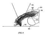
secondary particle detector 205, such as a channel detector electron multiplier (CDEM) that detects secondary particles that are generated when ions in the primary ion beam impact the work piece. Typically, such particle detectors can detect either electrons or ions, depending upon the voltages applied to the collector. - Another problem caused by the magnetic field of the SEM objective is that some of the secondary particles emitted from the target are deflected away from the input of the secondary particle detector.
FIG. 8 is a charged particle simulation, showingion beam column 102,particle detector 205, andtrajectories 802 of secondary electrons.Particle detector 205 includes ascreen 804 held at a positive electrical potential to attract electrons and aninput 806 through which electrons pass to enterdetector 205.FIG. 8 shows that, in the presence of the magnetic field from the SEM objective lens, most of the electrons generated at the work piece surface by the impact of the ions in the primary beam do not enterinput 806 and are not therefore detected. - The problem is solved by strategically positioning the secondary particle detector, so that the magnetic field of the objective lens bends the trajectories of the secondary particles toward the input of the detector. The ideal position and orientation for the detector can be determined using a simulation in a manner similar to the manner in which the position of the flood gun above was positioned.
FIG. 9 shows that with proper placement and orientation of the detector, secondary particles generated byprimary ion beam 902follow trajectories 904 that lead them to the input ofdetector 205 in the presence ofmagnetic field 302.FIG. 10 is asimulation showing trajectories 1002 of electrons generated by the impact of the primary ion beam fromFIB 102.FIG. 10 shows that all of the particles enter theinput 806 of particle detector. -
FIG. 6 shows that thesecondary particle detector 205 is preferably located in a vertical plane that is perpendicular to a vertical plane containing the SEM optical axis. If a flood gun is present, the particle detector is located in the same vertical plane as the flood gun, but on the opposite side of the system, that is, the particle detector is in a half plane rotated 90 degrees clockwise (looking from above) from the half plane containing the SEM.FIG. 7 shows that the particle detector is oriented at anangle 710 of about 30 degrees from the work piece surface and that the detector is positioned adistance 712 of about 0.6 mm above the surface ofwork piece 600. TheFIB column 102 is positioned adistance 720 of about 16 mm abovesurface 600. - In another embodiment, a secondary particle detector 810 (shown in dashed outline) could be positioned as shown in
FIG. 8 at a place where the secondary particles would enter the detector, although this position could physically interfere with the flood gun, if one is present on the system. - One aspect of a preferred embodiment is the use of an SEM objective lens that has relatively constant thermal signature, even as the magnetic field is adjusted to change the focus. By constant thermal signature is meant that not only is the total power dissipation approximately constant in time, but the power dissipations at all spatial positions on the lens are also approximately constant in time. Such an SEM objective lens is described in assignee's co-pending application entitled "Improved Magnetic Lens," of Bierhoff et al., filed July 14, 2003, at the USPTO with Application No.
10/621,103 -
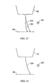
FIG. 11 shows apreferred SEM column 100. The SEM includes a magnetic objective lens 1104 as described in the above-referenced patent application and preferably useselectrostatic deflection 1106. Using electrostatic deflectors allows both the electron beam and the ion beam to be controlled using similar mechanisms, which makes system operation easier. Electrostatic deflectors also allow for fast scanning and do not produce the heat variation of magnetic deflectors. If magnetic deflectors were used, the current in magnetic deflectors would need to change as the magnification of the microscope is changed. Changing the deflector current would change the heat output, which adversely affects the stability of the system. - The magnetic field of the SEM lens also affects the trajectory of the ions in the primary ion beam. Although it is possible to steer the ion beam in a convention manner to compensate for the shift in position caused by the magnetic field, the resolution of the beam degrades in the presence of the magnetic field. Applicants have found that by using a liquid metal ion source of monoisotopic gallium, the resolution of the ion beam system is enhanced.
- Naturally occurring gallium is dual isotopic, that is, it is a mixture of two isotopes: one isotope, which comprises about 60 percent of the atoms in naturally occurring gallium, has an atomic mass of about 69 and a second isotope, which comprises about 40 percent of the atoms in naturally occurring gallium, has an atomic mass of about 71. The two isotopes are deflected differently in a strong magnetic field, so the different isotopes will split into two beams, which impact the target at slightly offset spots. This "double spot" results in poor image quality and poor resolution micromachining.
-
FIG. 12 shows the path ofgallium ions 1202 having an atomic mass of about 71 andgallium ions 1204 having an atomic mass of about 69 in themagnetic field 302 originating from the SEM objective lens. Themagnetic field 302 is in a direction into the plane of the paper.FIGS. 13A and 13B shows FIB images formed using naturally occurring, dual isotopic gallium ions from a gallium liquid metal ion source in the presence of a magnetic field from a SEM objective lens. InFIG. 13A , the magnetic field strength is at a minimum strength and the image is relatively sharp. InFIG. 13B , the magnetic field strength is at a maximum strength, and the image is noticeably blurry. -
FIG. 14 is similar toFIG 12 , but shows the use of monoisotopic gallium. Either of the two isotopes could be used. Monoisotopic gallium is used in time-of-flight mass spectrometers and so is readily available.FIG. 14 shows that with monoisotopic gallium, there is a single beam.FIGS. 15A and 15B shows FIB images formed using monoisotopic gallium ions from a gallium liquid metal ion source in the presence of a magnetic field from a SEM objective lens. InFIG. 15A , the magnetic field strength is at a minimum strength and the image is relatively sharp. InFIG. 15B , the magnetic field strength is at a maximum, and the image is still sharp. - Although the position of the beam landing will change as the magnetic field strength changes, the change in position can be compensated using the ion beam steering optics. There is no blurring in either image. Although monoisotopic gallium has been used in time-of-flight mass spectrometers, to applicants' knowledge it was not used in dual beam systems to overcome the problems caused by the action of the magnetic field on the gallium ion beam.
FIG. 7 shows that the FIB is positioned a distance 714 of 16 mm above the surface ofwork piece 600. - In a production environment, it is preferable that an operator can quickly move work pieces into and out of the dual beam system. Because the ion and electron beams operate in a vacuum chamber, it is necessary to open the chamber to remove or insert a work piece, and then the system must be evacuated again. The evacuation process is time consuming.
-
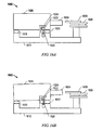
FIGS. 16A and 16B are block diagrams showing apreferred system 1602 that uses an "airlock"chamber 1604 that can be sealed and evacuated separately from aprimary vacuum system 1606. A work piece can be inserted into theairlock chamber 1604, which is sealed and can be evacuated while thesystem 1602 is operating with a primarysystem vacuum chamber 1606 that is evacuated. After theairlock chamber 1604 is evacuated, it can be opened to the primarysystem vacuum chamber 1606 and work pieces can be exchanged between the two chambers without requiring primarysystem vacuum chamber 1606 to be opened to the atmosphere. Arobotic arm 1608 loads a work piece, such aswafer 1609, onto a wafer holder (not shown) inairlock chamber 1604. Aframe 1612 supports the primary vacuum chamber and therobotic arm 1608. - The
airlock chamber 1604 preferably accommodates at least two work pieces, so that it can hold a new work piece and a completed work piece. Theairlock chamber 1604 preferably has a small volume to reduce the time required to evacuate it. - The high resolutions of the SEM and FIB make the system sensitive to vibration. The
primary vacuum chamber 1606, to which the ion and electron beam columns are mounted, "floats" onpneumatic cylinders 1610 above thesystem frame 1612 to stop the transmission of vibration from the floor.System 1602 typically includes an automatic leveler (not shown) that adjusts the air in thepneumatic cylinders 1610 so that thevacuum chamber 1606 system is level as it floats. To move the work piece to or from theairlock chamber 1604, it is necessary to "unfloat" theprimary chamber 1606 and precisely position theairlock chamber 1604 so that therobotic arm 1608 can accurately locate and lift the work piece into or out of theairlock 1604. In the prior art, this alignment typically entailed deflating thepneumatic cylinders 1610 that supports theprimary chamber 1606. Deflating thepneumatic cylinders 1610 takes time. - In a preferred embodiment, rather than deflating the
pneumatic cylinders 1610, theprimary chamber 1606 is forced up into a mating position, rather than being lowered into a mating position. The chamber can be forced up, for example, using a pneumatic orhydraulic cylinder 1620, an electric motor, or other means. Theprimary chamber 1606 is positioned, for example, by using two mating structures, onemating structure 1622 mounted on theprimary vacuum chamber 1606 and asecond mating structure 1624 mounted on theframe 1612. - For example, one or more acorn nuts mounted on the floating primary chamber can be forced into one or more mating holes mounted on the fixed system frame. Other alignment structures are well known. As the floating portion is forced up, the acorn nuts are forced into holes to align the primary chamber in three dimensions. One the airlock is aligned with the primary vacuum chamber, a
robotic arm 1608 mounted on the frame can move a work piece to the airlock and retrieve a wafer from the airlock. Preferably, the automatic leveling is turned off, and only the side of the primary chamber by the air lock is forced up. The slight angle of the primary chamber resulting from forcing only one side up does not interfere with the work piece transfer. After the work pieces are transferred, the primary chamber is released bycylinder 1620 and settles back onto thepneumatic cylinders 1610, the automatic leveling is activated, and system operation can continue. By docking in the "up" position, a significant amount of time is saved by making it unnecessary to deflate and then reinflate the pneumatic cylinders. - Although the present invention and its advantages have been described in detail, it should be understood that various changes, substitutions and alterations can be made herein without departing from the scope of the invention as defined by the appended claims. Moreover, the scope of the present application is not intended to be limited to the particular embodiments of the process, machine, manufacture, composition of matter, means, methods and steps described in the specification. As one of ordinary skill in the art will readily appreciate from the disclosure of the present invention, processes, machines, manufacture, compositions of matter, means, methods, or steps, presently existing or later to be developed that perform substantially the same function or achieve substantially the same result as the corresponding embodiments described herein may be utilized according to the present invention. Accordingly, the appended claims are intended to include within their scope such processes, machines, manufacture, compositions of matter, means, methods, or steps.
Claims (8)
- A dual beam system (96), comprising:• an ion beam column (102) for producing a primary ion beam, and• an electron beam column (100) having a magnetic objective lens (1104), characterized in that the system further comprises• an electron gun (204) not being part of the electron beam column to provide neutralizing electrons, the electron gun positioned so that the magnetic field (302) of the electron beam column assists in steering the neutralizing electrons to the target point of the focused ion beam column, the electron gun including steering electrodes (406, 502) to adjust the electron path (304) to compensate for changes in the magnetic field.
- The system of claim 1 further comprising a secondary particle collection device (205) for collecting secondary particles (802) generated by the primary ion beam, the secondary particle collection device positioned so that the magnetic field of the electron beam column assists in steering the secondary particles to the secondary particle collection device.
- The system of claim 1 or claim 2, in which the electron gun (204) includes a four electrode element (502) that focuses and steers the electron beam.
- The system of any of the preceding claims in which the electron gun (204) is composed of non-magnetic materials so as to reduce distortion of the magnetic field of the objective lens (1104).
- A method of operating a dual beam system (96), said dual beam system including an electron beam column (100) using a magnetic objective lens (1104) and an ion beam column (102), the method comprising:• directing a beam of ions towards a work piece (306),• applying a current to the magnetic objective lens of the electron beam column concurrently with directing the beam of ions towards the work piece, the current being the same current used when the electron beam column is directing electrons towards the work piece,characterised in that• low energy electrons are directed towards the work piece to neutralize at least some of the charge on the work piece while directing a beam of ions toward the work piece, said low energy electrons produced by an electron gun (204) separate from the electron beam column.
- The method of claim 5 in which the low energy electrons are steered to the work piece with the aid of the magnetic field of the magnetic objective lens.
- The method of claim 5 or claim 6 in which the low energy electrons are also steered to the work piece (306) with a four electrode steering element (406, 502) in the electron gun (204).
- The method of any of claims 5-7 in which secondary particles (802) emanating from the work piece (306) as a result of the ion beam impinging on the work piece are collected by a secondary particle collection device (205), said secondary particle collection device positioned so that the magnetic field of the electron beam column (100) assists in steering the secondary particles to the secondary particle collection device.
Applications Claiming Priority (2)
| Application Number | Priority Date | Filing Date | Title |
|---|---|---|---|
| US48779203P | 2003-07-14 | 2003-07-14 | |
| US487792 | 2003-07-14 |
Publications (3)
| Publication Number | Publication Date |
|---|---|
| EP1501115A2 EP1501115A2 (en) | 2005-01-26 |
| EP1501115A3 EP1501115A3 (en) | 2007-09-05 |
| EP1501115B1 true EP1501115B1 (en) | 2009-07-01 |
Family
ID=34135083
Family Applications (1)
| Application Number | Title | Priority Date | Filing Date |
|---|---|---|---|
| EP04076891A Active EP1501115B1 (en) | 2003-07-14 | 2004-07-01 | Dual beam system |
Country Status (4)
| Country | Link |
|---|---|
| US (4) | US7161159B2 (en) |
| EP (1) | EP1501115B1 (en) |
| JP (2) | JP2005038853A (en) |
| DE (1) | DE602004021750D1 (en) |
Cited By (1)
| Publication number | Priority date | Publication date | Assignee | Title |
|---|---|---|---|---|
| US9857318B2 (en) | 2013-03-19 | 2018-01-02 | Carl Zeiss Microscopy Gmbh | Method for generating image data relating to an object and particle beam device for carrying out this method |
Families Citing this family (37)
| Publication number | Priority date | Publication date | Assignee | Title |
|---|---|---|---|---|
| JP4178741B2 (en) | 2000-11-02 | 2008-11-12 | 株式会社日立製作所 | Charged particle beam apparatus and sample preparation apparatus |
| DE602004021750D1 (en) * | 2003-07-14 | 2009-08-13 | Fei Co | Two beam system |
| JP4431459B2 (en) * | 2004-07-29 | 2010-03-17 | 株式会社日立ハイテクノロジーズ | Focused ion beam apparatus and focused ion beam irradiation method |
| EP1630849B1 (en) | 2004-08-27 | 2011-11-02 | Fei Company | Localized plasma processing |
| US7459676B2 (en) * | 2005-11-21 | 2008-12-02 | Thermo Finnigan Llc | MALDI/LDI source |
| CN101461026B (en) * | 2006-06-07 | 2012-01-18 | Fei公司 | Slider bearing for use with an apparatus comprising a vacuum chamber |
| US8837677B2 (en) * | 2007-04-11 | 2014-09-16 | The Invention Science Fund I Llc | Method and system for compton scattered X-ray depth visualization, imaging, or information provider |
| US20080253627A1 (en) * | 2007-04-11 | 2008-10-16 | Searete LLC, a limited liability corporation of | Compton scattered X-ray visualization, imaging, or information provider using image combining |
| US20080253527A1 (en) * | 2007-04-11 | 2008-10-16 | Searete Llc, A Limited Liability Corporation Of The State Of Delaware | Limiting compton scattered x-ray visualizing, imaging, or information providing at particular regions |
| US20080253522A1 (en) * | 2007-04-11 | 2008-10-16 | Searete Llc, A Limited Liability Corporation Of The State Of Delaware | Tool associated with compton scattered X-ray visualization, imaging, or information provider |
| US7623625B2 (en) * | 2007-04-11 | 2009-11-24 | Searete Llc | Compton scattered X-ray visualization, imaging, or information provider with scattering event locating |
| US7711089B2 (en) | 2007-04-11 | 2010-05-04 | The Invention Science Fund I, Llc | Scintillator aspects of compton scattered X-ray visualization, imaging, or information providing |
| US20080253525A1 (en) * | 2007-04-11 | 2008-10-16 | Boyden Edward S | Compton scattered x-ray visualizing, imaging, or information providing of at least some dissimilar matter |
| US8041006B2 (en) * | 2007-04-11 | 2011-10-18 | The Invention Science Fund I Llc | Aspects of compton scattered X-ray visualization, imaging, or information providing |
| EP2006881A3 (en) | 2007-06-18 | 2010-01-06 | FEI Company | In-chamber electron detector |
| US20090006842A1 (en) * | 2007-06-26 | 2009-01-01 | John Gordon Ross | Sealing Electronic Data Associated With Multiple Electronic Documents |
| WO2009089499A2 (en) * | 2008-01-09 | 2009-07-16 | Fei Company | Multibeam system |
| DE102008041815A1 (en) | 2008-09-04 | 2010-04-15 | Carl Zeiss Nts Gmbh | Method for analyzing a sample |
| JP5702552B2 (en) * | 2009-05-28 | 2015-04-15 | エフ イー アイ カンパニFei Company | Control method of dual beam system |
| US20120119087A1 (en) * | 2009-08-03 | 2012-05-17 | Hitachi High-Technologies Corporation | Charged-particle microscope |
| EP2284524B1 (en) * | 2009-08-10 | 2014-01-15 | FEI Company | Microcalorimetry for X-ray spectroscopy |
| DE102010024625A1 (en) * | 2010-06-22 | 2011-12-22 | Carl Zeiss Nts Gmbh | Method for editing an object |
| DE102011006588A1 (en) * | 2011-03-31 | 2012-10-04 | Carl Zeiss Nts Gmbh | Particle beam device with detector arrangement |
| US9941096B2 (en) | 2011-09-12 | 2018-04-10 | Fei Company | Glancing angle mill |
| JP2013178876A (en) * | 2012-02-28 | 2013-09-09 | Hitachi High-Technologies Corp | Charged particle beam device |
| CN102636505B (en) * | 2012-03-20 | 2013-11-13 | 中国科学院合肥物质科学研究院 | Method for synchronously detecting single-ion-beam and double-channel signals |
| JP5969233B2 (en) * | 2012-03-22 | 2016-08-17 | 株式会社日立ハイテクサイエンス | Cross-section processing observation method and apparatus |
| DE112013001373B4 (en) * | 2012-04-03 | 2019-08-08 | Hitachi High-Technologies Corporation | Apparatus charged with a charged particle beam |
| CN102629541B (en) * | 2012-04-25 | 2016-02-17 | 中微半导体设备(上海)有限公司 | Spray head and forming method thereof |
| US8859982B2 (en) | 2012-09-14 | 2014-10-14 | Kla-Tencor Corporation | Dual-lens-gun electron beam apparatus and methods for high-resolution imaging with both high and low beam currents |
| US9991090B2 (en) | 2012-11-15 | 2018-06-05 | Fei Company | Dual laser beam system used with an electron microscope and FIB |
| CN105264635B (en) | 2012-12-31 | 2018-11-20 | Fei 公司 | Reference design for inclination or graze grinding operation using charged particle beam |
| KR102101350B1 (en) | 2013-03-15 | 2020-04-17 | 삼성전자주식회사 | particle counter and immersion scanner used the same |
| US10056228B2 (en) | 2014-07-29 | 2018-08-21 | Applied Materials Israel Ltd. | Charged particle beam specimen inspection system and method for operation thereof |
| US10037862B2 (en) * | 2015-07-31 | 2018-07-31 | Carl Zeiss Microscopy, Llc | Charged particle detecting device and charged particle beam system with same |
| US10242842B2 (en) * | 2016-03-25 | 2019-03-26 | Hitachi High-Tech Science Corporation | Method for cross-section processing and observation and apparatus therefor |
| DE102019203579A1 (en) | 2019-03-15 | 2020-09-17 | Carl Zeiss Microscopy Gmbh | Method for operating a particle beam device and particle beam device for carrying out the method |
Family Cites Families (69)
| Publication number | Priority date | Publication date | Assignee | Title |
|---|---|---|---|---|
| NL294153A (en) | 1962-06-25 | |||
| US3699334A (en) | 1969-06-16 | 1972-10-17 | Kollsman Instr Corp | Apparatus using a beam of positive ions for controlled erosion of surfaces |
| US4345152A (en) * | 1980-08-11 | 1982-08-17 | The Perkin-Elmer Corporation | Magnetic lens |
| JPS5981850A (en) * | 1982-11-02 | 1984-05-11 | Internatl Precision Inc | Electron lens |
| JPH0760657B2 (en) | 1985-08-22 | 1995-06-28 | 株式会社日立製作所 | Electron beam exposure system |
| US4818872A (en) * | 1987-05-11 | 1989-04-04 | Microbeam Inc. | Integrated charge neutralization and imaging system |
| JPS6417364A (en) | 1987-07-13 | 1989-01-20 | Mitsubishi Electric Corp | Electron beam device |
| JP2863558B2 (en) * | 1989-08-25 | 1999-03-03 | 株式会社日立製作所 | Charge neutralizer for focused ion beam equipment |
| JPH03117711A (en) | 1989-09-28 | 1991-05-20 | Nec Corp | Method of fitting surface-mounting connector on circuit board |
| US5093572A (en) | 1989-11-02 | 1992-03-03 | Mitsubishi Denki Kabushiki Kaisha | Scanning electron microscope for observation of cross section and method of observing cross section employing the same |
| JP2920390B2 (en) | 1989-11-08 | 1999-07-19 | 株式会社日立製作所 | Electronic lens cooling system |
| JPH03234417A (en) | 1990-02-08 | 1991-10-18 | Mitsubishi Electric Corp | Wire electric discharge machining method |
| JPH03117711U (en) * | 1990-03-19 | 1991-12-05 | ||
| JPH0473847A (en) * | 1990-07-12 | 1992-03-09 | Matsushita Electric Ind Co Ltd | Electron radiation device |
| GB9022945D0 (en) | 1990-10-22 | 1990-12-05 | Gillette Co | Safety razors |
| WO1994013010A1 (en) | 1991-04-15 | 1994-06-09 | Fei Company | Process of shaping features of semiconductor devices |
| US5206516A (en) | 1991-04-29 | 1993-04-27 | International Business Machines Corporation | Low energy, steered ion beam deposition system having high current at low pressure |
| JP2774884B2 (en) | 1991-08-22 | 1998-07-09 | 株式会社日立製作所 | Method for separating sample and method for analyzing separated sample obtained by this separation method |
| JP3082110B2 (en) | 1992-05-19 | 2000-08-28 | 松下電器産業株式会社 | Water detection circuit |
| JP3234373B2 (en) * | 1992-11-06 | 2001-12-04 | 株式会社日立製作所 | Magnetic field type electron lens and electron beam device using the same |
| JP3117836B2 (en) | 1993-03-02 | 2000-12-18 | セイコーインスツルメンツ株式会社 | Focused ion beam equipment |
| JPH07230784A (en) * | 1994-02-16 | 1995-08-29 | Jeol Ltd | Composite charge particle beam device |
| JPH06318443A (en) | 1994-03-31 | 1994-11-15 | Hitachi Ltd | Ion beam device |
| JP3152844B2 (en) | 1994-09-07 | 2001-04-03 | 旭化成マイクロシステム株式会社 | Gm-C filter |
| JP3234417B2 (en) | 1994-10-07 | 2001-12-04 | 本田技研工業株式会社 | Load sensor |
| JPH08115696A (en) | 1994-10-19 | 1996-05-07 | Jeol Ltd | Coil for electromagnet |
| EP0840940B1 (en) * | 1995-07-25 | 2000-06-14 | Nmi Naturwissenschaftliches Und Medizinisches Intitut An Der Universität Tübingen In Reutlingen | Process and device for ion thinning in a high-resolution transmission electron microscope |
| US5825038A (en) | 1996-11-26 | 1998-10-20 | Eaton Corporation | Large area uniform ion beam formation |
| JPH09257670A (en) | 1996-03-19 | 1997-10-03 | Hitachi Ltd | Specimen preparing apparatus for electron microscope |
| US6051839A (en) * | 1996-06-07 | 2000-04-18 | Arch Development Corporation | Magnetic lens apparatus for use in high-resolution scanning electron microscopes and lithographic processes |
| US5990476A (en) * | 1996-12-17 | 1999-11-23 | Physical Electronics Inc | Control of surface potential of insulating specimens in surface analysis |
| JPH10213422A (en) | 1997-01-29 | 1998-08-11 | Hitachi Ltd | Pattern inspecting device |
| US6332962B1 (en) * | 1997-06-13 | 2001-12-25 | Micrion Corporation | Thin-film magnetic recording head manufacture using selective imaging |
| US6538254B1 (en) | 1997-07-22 | 2003-03-25 | Hitachi, Ltd. | Method and apparatus for sample fabrication |
| JPH11154479A (en) * | 1997-11-20 | 1999-06-08 | Hitachi Ltd | Secondary electron image detection method and its device, and treatment method by focused charged particle beam and its device |
| JPH11238483A (en) * | 1997-12-12 | 1999-08-31 | Hitachi Ltd | Charged particle beam device |
| US6039000A (en) * | 1998-02-11 | 2000-03-21 | Micrion Corporation | Focused particle beam systems and methods using a tilt column |
| US6335532B1 (en) * | 1998-02-27 | 2002-01-01 | Hitachi, Ltd. | Convergent charged particle beam apparatus and inspection method using same |
| JP2992688B2 (en) * | 1998-05-19 | 1999-12-20 | セイコーインスツルメンツ株式会社 | Complex charged particle beam device |
| JP3041600B2 (en) | 1998-05-19 | 2000-05-15 | セイコーインスツルメンツ株式会社 | Complex charged particle beam device |
| JP3117950B2 (en) * | 1998-05-21 | 2000-12-18 | セイコーインスツルメンツ株式会社 | Charged particle device |
| US6344750B1 (en) * | 1999-01-08 | 2002-02-05 | Schlumberger Technologies, Inc. | Voltage contrast method for semiconductor inspection using low voltage particle beam |
| US6130432A (en) | 1999-04-13 | 2000-10-10 | International Business Machines Corporation | Particle beam system with dynamic focusing |
| US6414307B1 (en) * | 1999-07-09 | 2002-07-02 | Fei Company | Method and apparatus for enhancing yield of secondary ions |
| US6727500B1 (en) | 2000-02-25 | 2004-04-27 | Fei Company | System for imaging a cross-section of a substrate |
| US6683320B2 (en) * | 2000-05-18 | 2004-01-27 | Fei Company | Through-the-lens neutralization for charged particle beam system |
| WO2001097245A2 (en) * | 2000-06-15 | 2001-12-20 | Kla-Tencor, Inc. | Sectored magnetic lens and method of use |
| JP3951590B2 (en) * | 2000-10-27 | 2007-08-01 | 株式会社日立製作所 | Charged particle beam equipment |
| JP4178741B2 (en) * | 2000-11-02 | 2008-11-12 | 株式会社日立製作所 | Charged particle beam apparatus and sample preparation apparatus |
| US6770867B2 (en) * | 2001-06-29 | 2004-08-03 | Fei Company | Method and apparatus for scanned instrument calibration |
| JPWO2002075806A1 (en) * | 2001-03-16 | 2004-07-08 | 株式会社日立製作所 | Wafer inspection method, focused ion beam device, and transmitted electron beam device |
| DE60111496T2 (en) | 2001-04-24 | 2005-12-15 | Advantest Corp. | Rasterteilchenspiegelmikroskop |
| WO2003012551A1 (en) * | 2001-07-27 | 2003-02-13 | Fei Company | Electron beam processing |
| DE10233002B4 (en) | 2002-07-19 | 2006-05-04 | Leo Elektronenmikroskopie Gmbh | Objective lens for an electron microscopy system and electron microscopy system |
| EP1388883B1 (en) * | 2002-08-07 | 2013-06-05 | Fei Company | Coaxial FIB-SEM column |
| US7504182B2 (en) | 2002-09-18 | 2009-03-17 | Fei Company | Photolithography mask repair |
| JP2004146402A (en) | 2002-10-21 | 2004-05-20 | Advantest Corp | Electron beam exposure system and method for correcting deflection amount |
| JP4088533B2 (en) * | 2003-01-08 | 2008-05-21 | 株式会社日立ハイテクノロジーズ | Sample preparation apparatus and sample preparation method |
| DE602004021750D1 (en) | 2003-07-14 | 2009-08-13 | Fei Co | Two beam system |
| US6852982B1 (en) * | 2003-07-14 | 2005-02-08 | Fei Company | Magnetic lens |
| JP4073847B2 (en) | 2003-08-25 | 2008-04-09 | エスアイアイ・ナノテクノロジー株式会社 | Scanning probe microscope and scanning method |
| JP4431459B2 (en) | 2004-07-29 | 2010-03-17 | 株式会社日立ハイテクノロジーズ | Focused ion beam apparatus and focused ion beam irradiation method |
| JP5371142B2 (en) | 2006-07-14 | 2013-12-18 | エフ・イ−・アイ・カンパニー | Multi-source plasma focused ion beam system |
| US8303833B2 (en) | 2007-06-21 | 2012-11-06 | Fei Company | High resolution plasma etch |
| JP5873227B2 (en) | 2007-12-06 | 2016-03-01 | エフ・イ−・アイ・カンパニー | Slice and view with decoration |
| WO2009089499A2 (en) | 2008-01-09 | 2009-07-16 | Fei Company | Multibeam system |
| US10493559B2 (en) | 2008-07-09 | 2019-12-03 | Fei Company | Method and apparatus for laser machining |
| US8168961B2 (en) | 2008-11-26 | 2012-05-01 | Fei Company | Charged particle beam masking for laser ablation micromachining |
| EP2233907A1 (en) | 2009-03-27 | 2010-09-29 | FEI Company | Forming an image while milling a work piece |
-
2004
- 2004-07-01 DE DE602004021750T patent/DE602004021750D1/en active Active
- 2004-07-01 EP EP04076891A patent/EP1501115B1/en active Active
- 2004-07-13 US US10/889,967 patent/US7161159B2/en active Active
- 2004-07-14 JP JP2004206750A patent/JP2005038853A/en active Pending
-
2006
- 2006-12-18 US US11/641,540 patent/US7601976B2/en active Active
-
2009
- 2009-10-09 US US12/576,914 patent/US8013311B2/en active Active
-
2011
- 2011-07-26 JP JP2011163178A patent/JP5432220B2/en active Active
- 2011-08-31 US US13/222,536 patent/US8399864B2/en active Active
Cited By (1)
| Publication number | Priority date | Publication date | Assignee | Title |
|---|---|---|---|---|
| US9857318B2 (en) | 2013-03-19 | 2018-01-02 | Carl Zeiss Microscopy Gmbh | Method for generating image data relating to an object and particle beam device for carrying out this method |
Also Published As
| Publication number | Publication date |
|---|---|
| DE602004021750D1 (en) | 2009-08-13 |
| US7601976B2 (en) | 2009-10-13 |
| JP2005038853A (en) | 2005-02-10 |
| JP5432220B2 (en) | 2014-03-05 |
| US20050035291A1 (en) | 2005-02-17 |
| EP1501115A2 (en) | 2005-01-26 |
| EP1501115A3 (en) | 2007-09-05 |
| US8399864B2 (en) | 2013-03-19 |
| US20110309263A1 (en) | 2011-12-22 |
| US20100025578A1 (en) | 2010-02-04 |
| US20080035860A1 (en) | 2008-02-14 |
| US8013311B2 (en) | 2011-09-06 |
| US7161159B2 (en) | 2007-01-09 |
| JP2011210740A (en) | 2011-10-20 |
Similar Documents
| Publication | Publication Date | Title |
|---|---|---|
| EP1501115B1 (en) | Dual beam system | |
| US10522327B2 (en) | Method of operating a charged particle beam specimen inspection system | |
| KR102295389B1 (en) | A method for examining a sample using an array of primary charged particle beamlets, a charged particle beam device for examining a sample using an array of primary charged particle beamlets, and a multi-column microscope for examining a sample | |
| EP2365514B1 (en) | Twin beam charged particle column and method of operating thereof | |
| JP4215282B2 (en) | SEM equipped with electrostatic objective lens and electrical scanning device | |
| JP5498955B2 (en) | Apparatus and method for analyzing and / or processing samples | |
| KR101015116B1 (en) | Charged particle beam system | |
| US9053899B2 (en) | Method for imaging a sample in a charged particle apparatus | |
| EP1745492A1 (en) | Multi-column charged particle optics assembly | |
| JP6404736B2 (en) | Compound charged particle beam system | |
| US7034297B2 (en) | Method and system for use in the monitoring of samples with a charged particle beam | |
| US4929839A (en) | Focused ion beam column | |
| KR20200119839A (en) | Multi-beam inspection apparatus with improved detection performance of signal electrons | |
| US8987692B2 (en) | High brightness electron gun, system using the same, and method of operating thereof | |
| EP2182543B1 (en) | Method and device for improved alignment of a high brightness charged particle gun | |
| TW202326788A (en) | High resolution, multi-electron beam apparatus |
Legal Events
| Date | Code | Title | Description |
|---|---|---|---|
| PUAI | Public reference made under article 153(3) epc to a published international application that has entered the european phase |
Free format text: ORIGINAL CODE: 0009012 |
|
| 17P | Request for examination filed |
Effective date: 20040701 |
|
| AK | Designated contracting states |
Kind code of ref document: A2 Designated state(s): AT BE BG CH CY CZ DE DK EE ES FI FR GB GR HU IE IT LI LU MC NL PL PT RO SE SI SK TR |
|
| AX | Request for extension of the european patent |
Extension state: AL HR LT LV MK |
|
| PUAL | Search report despatched |
Free format text: ORIGINAL CODE: 0009013 |
|
| AK | Designated contracting states |
Kind code of ref document: A3 Designated state(s): AT BE BG CH CY CZ DE DK EE ES FI FR GB GR HU IE IT LI LU MC NL PL PT RO SE SI SK TR |
|
| AX | Request for extension of the european patent |
Extension state: AL HR LT LV MK |
|
| RIC1 | Information provided on ipc code assigned before grant |
Ipc: H01J 37/10 20060101ALI20070727BHEP Ipc: H01J 37/30 20060101AFI20041123BHEP Ipc: H01J 37/26 20060101ALI20070727BHEP |
|
| 17Q | First examination report despatched |
Effective date: 20071009 |
|
| AKX | Designation fees paid |
Designated state(s): CZ DE FR GB NL |
|
| GRAP | Despatch of communication of intention to grant a patent |
Free format text: ORIGINAL CODE: EPIDOSNIGR1 |
|
| RIN1 | Information on inventor provided before grant (corrected) |
Inventor name: DIMANNA, MARK Inventor name: TANGUAY, MICHAEL Inventor name: HILL, RAY Inventor name: SANFORD, COLIN Inventor name: SCIPIONI, LAWRENCE |
|
| GRAS | Grant fee paid |
Free format text: ORIGINAL CODE: EPIDOSNIGR3 |
|
| GRAA | (expected) grant |
Free format text: ORIGINAL CODE: 0009210 |
|
| AK | Designated contracting states |
Kind code of ref document: B1 Designated state(s): CZ DE FR GB NL |
|
| REG | Reference to a national code |
Ref country code: GB Ref legal event code: FG4D |
|
| REF | Corresponds to: |
Ref document number: 602004021750 Country of ref document: DE Date of ref document: 20090813 Kind code of ref document: P |
|
| NLV1 | Nl: lapsed or annulled due to failure to fulfill the requirements of art. 29p and 29m of the patents act | ||
| PG25 | Lapsed in a contracting state [announced via postgrant information from national office to epo] |
Ref country code: NL Free format text: LAPSE BECAUSE OF FAILURE TO SUBMIT A TRANSLATION OF THE DESCRIPTION OR TO PAY THE FEE WITHIN THE PRESCRIBED TIME-LIMIT Effective date: 20090701 |
|
| PG25 | Lapsed in a contracting state [announced via postgrant information from national office to epo] |
Ref country code: CZ Free format text: LAPSE BECAUSE OF FAILURE TO SUBMIT A TRANSLATION OF THE DESCRIPTION OR TO PAY THE FEE WITHIN THE PRESCRIBED TIME-LIMIT Effective date: 20090701 |
|
| PLBE | No opposition filed within time limit |
Free format text: ORIGINAL CODE: 0009261 |
|
| STAA | Information on the status of an ep patent application or granted ep patent |
Free format text: STATUS: NO OPPOSITION FILED WITHIN TIME LIMIT |
|
| 26N | No opposition filed |
Effective date: 20100406 |
|
| REG | Reference to a national code |
Ref country code: FR Ref legal event code: PLFP Year of fee payment: 13 |
|
| REG | Reference to a national code |
Ref country code: FR Ref legal event code: PLFP Year of fee payment: 14 |
|
| REG | Reference to a national code |
Ref country code: FR Ref legal event code: PLFP Year of fee payment: 15 |
|
| P01 | Opt-out of the competence of the unified patent court (upc) registered |
Effective date: 20230520 |
|
| PGFP | Annual fee paid to national office [announced via postgrant information from national office to epo] |
Ref country code: GB Payment date: 20230728 Year of fee payment: 20 |
|
| PGFP | Annual fee paid to national office [announced via postgrant information from national office to epo] |
Ref country code: FR Payment date: 20230728 Year of fee payment: 20 Ref country code: DE Payment date: 20230724 Year of fee payment: 20 |