EP1505648A2 - Active matrix display device - Google Patents
Active matrix display device Download PDFInfo
- Publication number
- EP1505648A2 EP1505648A2 EP04078120A EP04078120A EP1505648A2 EP 1505648 A2 EP1505648 A2 EP 1505648A2 EP 04078120 A EP04078120 A EP 04078120A EP 04078120 A EP04078120 A EP 04078120A EP 1505648 A2 EP1505648 A2 EP 1505648A2
- Authority
- EP
- European Patent Office
- Prior art keywords
- insulating layer
- film
- bank
- active matrix
- organic semiconductive
- Prior art date
- Legal status (The legal status is an assumption and is not a legal conclusion. Google has not performed a legal analysis and makes no representation as to the accuracy of the status listed.)
- Ceased
Links
- 239000011159 matrix material Substances 0.000 title claims abstract description 100
- 238000000034 method Methods 0.000 claims abstract description 35
- 230000008569 process Effects 0.000 claims abstract description 31
- 239000011368 organic material Substances 0.000 claims abstract description 24
- 239000000758 substrate Substances 0.000 claims description 33
- 229910010272 inorganic material Inorganic materials 0.000 claims description 31
- 239000011147 inorganic material Substances 0.000 claims description 31
- 230000002093 peripheral effect Effects 0.000 claims description 9
- 239000005871 repellent Substances 0.000 claims description 5
- 239000010408 film Substances 0.000 abstract description 276
- 239000010409 thin film Substances 0.000 abstract description 42
- 230000015572 biosynthetic process Effects 0.000 abstract description 25
- 230000003071 parasitic effect Effects 0.000 abstract description 23
- 239000010410 layer Substances 0.000 description 345
- 230000003247 decreasing effect Effects 0.000 description 19
- 239000003990 capacitor Substances 0.000 description 18
- 238000010586 diagram Methods 0.000 description 14
- VYPSYNLAJGMNEJ-UHFFFAOYSA-N Silicium dioxide Chemical compound O=[Si]=O VYPSYNLAJGMNEJ-UHFFFAOYSA-N 0.000 description 13
- 229920001721 polyimide Polymers 0.000 description 13
- 229910052814 silicon oxide Inorganic materials 0.000 description 13
- 239000000243 solution Substances 0.000 description 13
- 229910052581 Si3N4 Inorganic materials 0.000 description 12
- 239000011229 interlayer Substances 0.000 description 12
- HQVNEWCFYHHQES-UHFFFAOYSA-N silicon nitride Chemical compound N12[Si]34N5[Si]62N3[Si]51N64 HQVNEWCFYHHQES-UHFFFAOYSA-N 0.000 description 12
- 239000002243 precursor Substances 0.000 description 10
- 230000000694 effects Effects 0.000 description 9
- 238000005530 etching Methods 0.000 description 8
- 230000004048 modification Effects 0.000 description 8
- 238000012986 modification Methods 0.000 description 8
- 238000000059 patterning Methods 0.000 description 7
- 238000000623 plasma-assisted chemical vapour deposition Methods 0.000 description 7
- 230000000740 bleeding effect Effects 0.000 description 5
- 230000006866 deterioration Effects 0.000 description 5
- BOTDANWDWHJENH-UHFFFAOYSA-N Tetraethyl orthosilicate Chemical compound CCO[Si](OCC)(OCC)OCC BOTDANWDWHJENH-UHFFFAOYSA-N 0.000 description 4
- 238000000151 deposition Methods 0.000 description 4
- 230000008021 deposition Effects 0.000 description 4
- 238000002347 injection Methods 0.000 description 4
- 239000007924 injection Substances 0.000 description 4
- 239000004973 liquid crystal related substance Substances 0.000 description 4
- 230000007547 defect Effects 0.000 description 3
- 238000007599 discharging Methods 0.000 description 3
- 239000011344 liquid material Substances 0.000 description 3
- 238000004020 luminiscence type Methods 0.000 description 3
- 239000002904 solvent Substances 0.000 description 3
- 229910052782 aluminium Inorganic materials 0.000 description 2
- XAGFODPZIPBFFR-UHFFFAOYSA-N aluminium Chemical compound [Al] XAGFODPZIPBFFR-UHFFFAOYSA-N 0.000 description 2
- 229910021417 amorphous silicon Inorganic materials 0.000 description 2
- QVGXLLKOCUKJST-UHFFFAOYSA-N atomic oxygen Chemical compound [O] QVGXLLKOCUKJST-UHFFFAOYSA-N 0.000 description 2
- 230000004888 barrier function Effects 0.000 description 2
- 238000000576 coating method Methods 0.000 description 2
- 230000000052 comparative effect Effects 0.000 description 2
- 230000000295 complement effect Effects 0.000 description 2
- 239000007789 gas Substances 0.000 description 2
- 238000010438 heat treatment Methods 0.000 description 2
- 238000004519 manufacturing process Methods 0.000 description 2
- 239000000463 material Substances 0.000 description 2
- 229910052751 metal Inorganic materials 0.000 description 2
- 239000002184 metal Substances 0.000 description 2
- 229910052760 oxygen Inorganic materials 0.000 description 2
- 239000001301 oxygen Substances 0.000 description 2
- 229920000553 poly(phenylenevinylene) Polymers 0.000 description 2
- -1 polyphenylene vinylene Polymers 0.000 description 2
- 230000001681 protective effect Effects 0.000 description 2
- 239000002356 single layer Substances 0.000 description 2
- 238000004544 sputter deposition Methods 0.000 description 2
- OYPRJOBELJOOCE-UHFFFAOYSA-N Calcium Chemical compound [Ca] OYPRJOBELJOOCE-UHFFFAOYSA-N 0.000 description 1
- WHXSMMKQMYFTQS-UHFFFAOYSA-N Lithium Chemical compound [Li] WHXSMMKQMYFTQS-UHFFFAOYSA-N 0.000 description 1
- ZOKXTWBITQBERF-UHFFFAOYSA-N Molybdenum Chemical compound [Mo] ZOKXTWBITQBERF-UHFFFAOYSA-N 0.000 description 1
- XUIMIQQOPSSXEZ-UHFFFAOYSA-N Silicon Chemical compound [Si] XUIMIQQOPSSXEZ-UHFFFAOYSA-N 0.000 description 1
- RTAQQCXQSZGOHL-UHFFFAOYSA-N Titanium Chemical compound [Ti] RTAQQCXQSZGOHL-UHFFFAOYSA-N 0.000 description 1
- 238000009825 accumulation Methods 0.000 description 1
- 229910052791 calcium Inorganic materials 0.000 description 1
- 239000011575 calcium Substances 0.000 description 1
- 238000002425 crystallisation Methods 0.000 description 1
- 230000008025 crystallization Effects 0.000 description 1
- 238000005265 energy consumption Methods 0.000 description 1
- 239000012535 impurity Substances 0.000 description 1
- AMGQUBHHOARCQH-UHFFFAOYSA-N indium;oxotin Chemical compound [In].[Sn]=O AMGQUBHHOARCQH-UHFFFAOYSA-N 0.000 description 1
- 238000009434 installation Methods 0.000 description 1
- 238000009413 insulation Methods 0.000 description 1
- 230000001788 irregular Effects 0.000 description 1
- 238000005224 laser annealing Methods 0.000 description 1
- 229910052744 lithium Inorganic materials 0.000 description 1
- 229910052750 molybdenum Inorganic materials 0.000 description 1
- 239000011733 molybdenum Substances 0.000 description 1
- 229910052698 phosphorus Inorganic materials 0.000 description 1
- 239000011574 phosphorus Substances 0.000 description 1
- 229910021420 polycrystalline silicon Inorganic materials 0.000 description 1
- 229920005591 polysilicon Polymers 0.000 description 1
- 230000002035 prolonged effect Effects 0.000 description 1
- 230000009467 reduction Effects 0.000 description 1
- 229910052710 silicon Inorganic materials 0.000 description 1
- 239000010703 silicon Substances 0.000 description 1
- 239000007790 solid phase Substances 0.000 description 1
- 229910052715 tantalum Inorganic materials 0.000 description 1
- GUVRBAGPIYLISA-UHFFFAOYSA-N tantalum atom Chemical compound [Ta] GUVRBAGPIYLISA-UHFFFAOYSA-N 0.000 description 1
- 229910052719 titanium Inorganic materials 0.000 description 1
- 239000010936 titanium Substances 0.000 description 1
- WFKWXMTUELFFGS-UHFFFAOYSA-N tungsten Chemical compound [W] WFKWXMTUELFFGS-UHFFFAOYSA-N 0.000 description 1
- 229910052721 tungsten Inorganic materials 0.000 description 1
- 239000010937 tungsten Substances 0.000 description 1
Images


Classifications
-
- H—ELECTRICITY
- H10—SEMICONDUCTOR DEVICES; ELECTRIC SOLID-STATE DEVICES NOT OTHERWISE PROVIDED FOR
- H10K—ORGANIC ELECTRIC SOLID-STATE DEVICES
- H10K59/00—Integrated devices, or assemblies of multiple devices, comprising at least one organic light-emitting element covered by group H10K50/00
- H10K59/10—OLED displays
- H10K59/12—Active-matrix OLED [AMOLED] displays
- H10K59/122—Pixel-defining structures or layers, e.g. banks
-
- G—PHYSICS
- G09—EDUCATION; CRYPTOGRAPHY; DISPLAY; ADVERTISING; SEALS
- G09F—DISPLAYING; ADVERTISING; SIGNS; LABELS OR NAME-PLATES; SEALS
- G09F9/00—Indicating arrangements for variable information in which the information is built-up on a support by selection or combination of individual elements
- G09F9/30—Indicating arrangements for variable information in which the information is built-up on a support by selection or combination of individual elements in which the desired character or characters are formed by combining individual elements
-
- H—ELECTRICITY
- H10—SEMICONDUCTOR DEVICES; ELECTRIC SOLID-STATE DEVICES NOT OTHERWISE PROVIDED FOR
- H10K—ORGANIC ELECTRIC SOLID-STATE DEVICES
- H10K50/00—Organic light-emitting devices
- H10K50/80—Constructional details
- H10K50/805—Electrodes
-
- H—ELECTRICITY
- H10—SEMICONDUCTOR DEVICES; ELECTRIC SOLID-STATE DEVICES NOT OTHERWISE PROVIDED FOR
- H10K—ORGANIC ELECTRIC SOLID-STATE DEVICES
- H10K59/00—Integrated devices, or assemblies of multiple devices, comprising at least one organic light-emitting element covered by group H10K50/00
- H10K59/10—OLED displays
- H10K59/12—Active-matrix OLED [AMOLED] displays
- H10K59/131—Interconnections, e.g. wiring lines or terminals
-
- H—ELECTRICITY
- H10—SEMICONDUCTOR DEVICES; ELECTRIC SOLID-STATE DEVICES NOT OTHERWISE PROVIDED FOR
- H10K—ORGANIC ELECTRIC SOLID-STATE DEVICES
- H10K59/00—Integrated devices, or assemblies of multiple devices, comprising at least one organic light-emitting element covered by group H10K50/00
- H10K59/80—Constructional details
- H10K59/805—Electrodes
-
- H—ELECTRICITY
- H10—SEMICONDUCTOR DEVICES; ELECTRIC SOLID-STATE DEVICES NOT OTHERWISE PROVIDED FOR
- H10K—ORGANIC ELECTRIC SOLID-STATE DEVICES
- H10K50/00—Organic light-emitting devices
- H10K50/80—Constructional details
- H10K50/86—Arrangements for improving contrast, e.g. preventing reflection of ambient light
- H10K50/865—Arrangements for improving contrast, e.g. preventing reflection of ambient light comprising light absorbing layers, e.g. light-blocking layers
-
- H—ELECTRICITY
- H10—SEMICONDUCTOR DEVICES; ELECTRIC SOLID-STATE DEVICES NOT OTHERWISE PROVIDED FOR
- H10K—ORGANIC ELECTRIC SOLID-STATE DEVICES
- H10K59/00—Integrated devices, or assemblies of multiple devices, comprising at least one organic light-emitting element covered by group H10K50/00
- H10K59/30—Devices specially adapted for multicolour light emission
- H10K59/35—Devices specially adapted for multicolour light emission comprising red-green-blue [RGB] subpixels
-
- H—ELECTRICITY
- H10—SEMICONDUCTOR DEVICES; ELECTRIC SOLID-STATE DEVICES NOT OTHERWISE PROVIDED FOR
- H10K—ORGANIC ELECTRIC SOLID-STATE DEVICES
- H10K59/00—Integrated devices, or assemblies of multiple devices, comprising at least one organic light-emitting element covered by group H10K50/00
- H10K59/80—Constructional details
- H10K59/8791—Arrangements for improving contrast, e.g. preventing reflection of ambient light
- H10K59/8792—Arrangements for improving contrast, e.g. preventing reflection of ambient light comprising light absorbing layers, e.g. black layers
-
- H—ELECTRICITY
- H10—SEMICONDUCTOR DEVICES; ELECTRIC SOLID-STATE DEVICES NOT OTHERWISE PROVIDED FOR
- H10K—ORGANIC ELECTRIC SOLID-STATE DEVICES
- H10K71/00—Manufacture or treatment specially adapted for the organic devices covered by this subclass
- H10K71/10—Deposition of organic active material
- H10K71/12—Deposition of organic active material using liquid deposition, e.g. spin coating
- H10K71/13—Deposition of organic active material using liquid deposition, e.g. spin coating using printing techniques, e.g. ink-jet printing or screen printing
- H10K71/135—Deposition of organic active material using liquid deposition, e.g. spin coating using printing techniques, e.g. ink-jet printing or screen printing using ink-jet printing
Definitions
- the present invention relates to active matrix display devices which control thin film luminescent devices, such as electroluminescent (EL) devices emitting light by a driving current flowing in an organic semiconductive film, and light-emitting diode (LED) devices using thin film transistors (hereinafter referred to as TFTs).
- thin film luminescent devices such as electroluminescent (EL) devices emitting light by a driving current flowing in an organic semiconductive film, and light-emitting diode (LED) devices using thin film transistors (hereinafter referred to as TFTs).
- Active matrix display devices using current-control-type luminescent devices such as EL devices or LED devices have been proposed. Since luminescent devices used in such types of display devices have self-luminescent functions; these have advantages, such as no installation of a backlight being necessary, whereas backlights are essential for liquid crystal display devices, and a wider viewing angle.
- Fig. 22 is a block diagram of an active matrix display device using charge-injection-type organic EL devices.
- a plurality of scanning lines gate, a plurality of data lines sig extending in the direction perpendicular to the direction of the scanning lines gate, a plurality of common feed lines com along the data lines sig, and a plurality of pixels 7 in a matrix formed by the data lines sig and the scanning lines gate are formed on a transparent substrate 10.
- a data line driving circuit 3 and a scanning line driving circuit 4 are provided for the data lines sig and the scanning lines gate, respectively.
- Each pixel 7 is provided with a conduction control circuit 50 for supplying scanning signals from a scanning line gate , and a thin film luminescent device 40 emitting light based on image signals supplied from a data line sig through the conduction control circuit 50.
- the conduction control circuit 50 has a first TFT 20 for supplying scanning signals from the scanning line gate to a gate electrode; a holding capacitor cap for holding image signals supplied from the data line sig through the first TFT 20; and a second TFT 30 for supplying the image signals held in the holding capacitor cap to the gate electrode.
- the second TFT 30 and the thin film luminescent device 40 are connected in series between an opposite electrode op (described below) and a common feed line com .
- the thin film luminescent device 40 emits light by a driving current from the common feed line com when the second TFT 30 is an ON mode, and this emitting mode is maintained by a holding capacitor cap for a predetermined time.
- the first TFT 20 and the second TFT 30 are formed of islands of a semiconductive film in each pixel 7.
- the first TFT 20 is provided with a gate electrode 21 as a part of a scanning line gate .
- one source-drain region is electrically connected to a data line sig through a contact hole in a first insulating interlayer 51, and the other region is connected to a drain electrode 22.
- the drain electrode 22 extends towards the region of the second TFT 30, and this extension is electrically connected to a gate electrode 31 of the second TFT 30 through a contact hole in the first insulating interlayer 51.
- One source-drain region of the second TFT 30 is electrically connected to a relay electrode 35 through a contact hole of the first insulating interlayer 51, and the relay electrode 35 is electrically connected to a pixel electrode 41 of the thin film luminescent device 40 through a contact hole in a second insulating interlayer 52.
- Each pixel electrode 41 is independently formed in each pixel 7, as shown in Figs. 23, 24(B), and 24(C).
- An organic semiconductive film 43 and an opposite electrode op are formed above the pixel electrode 41 in that order.
- the organic semiconductive film 43 is formed in each pixel 7, a stripe film may be formed over a plurality of pixels 7.
- the opposite electrode op is formed not only in a display section 11 including pixels 7, but also over the entire surface of the transparent substrate 10.
- the other source-drain region of the second TFT 30 is electrically connected to the common feed line com through a contact hole in the first insulating interlayer 51.
- An extension 39 of the common feed line com faces an extension 36 of the gate electrode 31 in the second TFT 30 separated by the first insulating interlayer 51 as a dielectric film to form a holding capacitor cap.
- the second insulating interlayer 52 is disposed between the opposite electrode op facing the pixel electrode 41 and the data line sig on the same transparent substrate 10, unlike liquid crystal active matrix display devices; hence, a large capacitance is formed in the data line sig and the data line driving circuit 3 is heavily loaded.
- the present inventors propose a reduction in parasitic capacitance in the data line sig by providing a thick insulating film (a bank layer bank; the region shaded with lines slanting downward to the left at a wide pitch) between the opposite electrode op and the data line sig . Furthermore, the present inventors propose that the region for forming the organic semiconductive film 43 be surrounded with the insulating film (bank layer bank) to contain any solution discharged from an ink-jet head and to prevent bleeding of the solution towards the sides during formation of the organic semiconductive film 43.
- the entire bank layer bank is formed of a thick inorganic material in adoption of such a configuration, a problem of a prolonged film forming time arises.
- the thick inorganic film is patterned, the pixel electrode 41 may be damaged due to overetching.
- the bank layer bank is formed of an organic material, such as a resist, the organic semiconductive film 43 may deteriorate at the boundary between the organic semiconductive film 43 and the bank layer bank by the effects of the solvent components contained in the organic material in the bank layer bank.
- the opposite electrode op formed above the bank layer bank readily breaks on the step difference bb .
- Such breakage of the opposite electrode op due to the step difference bb causes insulation of the opposite electrode op from the neighboring opposite electrodes op to form point or linear defects in the display.
- the opposite electrode op breaks along the outer periphery of the bank layer bank which covers the surfaces of the data line driving circuit 3 and the scanning line driving circuit 4, the opposite electrode op in the display section 11 is completely insulated from a terminal 12 and thus no image is displayed.
- an active matrix display device comprising a display region including a plurality of scanning lines on a substrate, a plurality of data lines extending in the direction perpendicular to the direction of the scanning lines, and a plurality of pixels arranged in a matrix delimited by the data lines and the scanning lines; each of the pixels being provided with a thin film luminescent device having a conduction control circuit containing a thin film transistor for supplying a scanning signal to a gate electrode through one of the scanning lines, a pixel electrode, an organic semiconductive film deposited above the pixel electrode, and an opposite electrode deposited above the organic semiconductive film; the thin film luminescent device emitting light based on an image signal supplied from the data line through the conduction control circuit; wherein the region for forming the organic semiconductive film is divided by an insulating film which is thicker than the organic semiconductive film; and the insulating film comprises a lower insulating layer which is formed of an inorganic material and is thicker
- the data line will form large parasitic capacitance if the opposite electrode is formed on the entire surface of the display section to face the data line; however, a thick insulating film is provided between the data line and the opposite electrode in the present invention to prevent formation of the parasitic capacitance in the data line.
- a load on the data line driving circuit is reduced, and low energy consumption and high-speed display operation are achieved.
- the thick insulating film is formed of only an inorganic material, a long film deposition time is required, resulting in low productivity.
- the lower insulating layer in contact with the organic semiconductive film of the thin film luminescent device is formed of an inorganic material, and an upper insulating layer composed of an organic material such as a resist is formed thereon. Since the upper insulating layer composed of an organic material facilitates formation of a thick film and so results in improved productivity.
- the upper insulating layer does not come into contact with the organic semiconductive film, but the lower insulating layer composed of an inorganic material does come into contact with the organic semiconductive film; hence, the organic semiconductive film is protected from deterioration affected by the upper insulating layer. Accordingly, the thin film luminescent device does not have any decreased luminescent efficiency or reliability.
- the upper insulating layer be deposited in an inner region of the lower insulating layer so as to have a width narrower than that of the upper insulating layer.
- Such a two-step configuration prevents contact of the upper insulating layer composed of an organic material with the organic semiconductive film; hence deterioration of the organic semiconductive film can be more securely prevented.
- both the lower insulating layer and the upper insulating layer may be formed of inorganic materials.
- Another aspect of the present invention is an active matrix display device comprising a display region including a plurality of scanning lines on a substrate, a plurality of data lines extending in the direction perpendicular to the direction of the scanning lines, and a plurality of pixels arranged in a matrix delimited by the data lines and the scanning lines; each of the pixels being provided with a thin film luminescent device having a conduction control circuit containing a thin film transistor for supplying a scanning signal to a gate electrode through one of the scanning lines, a pixel electrode, an organic semiconductive film deposited above the pixel electrode, and an opposite electrode deposited above the organic semiconductive film; the thin film luminescent device emitting light based on an image signal supplied from the data line through the conduction control circuit; wherein the region for forming the organic semiconductive film is divided by an insulating film which is thicker than the organic semiconductive film; and the insulating
- the upper insulating layer is patterned. Since the lower insulating layer functions as an etching stopper, the pixel electrodes will not be damaged by slight overetching. After the patterning, the lower insulating layer is patterned. Since only one layer of the lower insulating layer is etched, the etching is readily controlled so that overetching, which would damage the pixel electrodes, does not occur.
- the conduction control circuit be provided with a first TFT for supplying the scanning signal to the gate electrode and a second TFT of which the gate electrode is connected to the data line through the first TFT, and that the second TFT and the thin film luminescent device be connected in series between a common feed line formed in addition to the data line and the scanning line for supplying a drive current and the opposite electrode.
- the conduction control circuit can be composed of a TFT and a holding capacitor
- the conduction control circuit of each pixel is preferably composed of two TFTs and two holding capacitors for improving display quality.
- the insulating film be used as a bank layer which prevents bleeding of a discharged solution when the organic semiconductive film is formed by an ink-jet process in a region delimited by the insulating film.
- the insulating film preferably has a thickness of 1 ⁇ m or more.
- a region overlapping the area for forming the conduction control circuit in the region for forming the pixel electrode be covered with the insulating film. That is, it is preferable that within the region for forming the pixel electrode, the thick insulating film be opened only at the flat section not having the conduction control circuit and the organic semiconductive film be formed only at the interior thereof.
- the thick insulating film be opened only at the flat section not having the conduction control circuit and the organic semiconductive film be formed only at the interior thereof.
- Such a configuration can prevent display irregularities due to an irregular thickness of the organic semiconductive film.
- a thinner section of the organic semiconductive film causes a concentration of the driving current of the thin film luminescent device and decreased reliability; however, this configuration can prevent such a problem.
- the organic semiconductive film emits light due to a driving current between a pixel electrode and the opposite electrode in the region overlapping the conduction control circuit, the light is shaded by the conduction control circuit and does not contribute to display.
- the driving current not contributing to display by the shading effect of the conduction control circuit is an unavailable current.
- the thick insulating film is formed at the section, in which such an unavailable current is expected, to prevent formation of the unavailable current.
- a current in the common feed line can be reduced.
- a luminescent area can be increased, improving display characteristics, such as luminance and contrast.
- the corners delimited by the insulating film may be rounded so that the organic semiconductive film has a rounded planar shape.
- the organic semiconductive film having such a shape avoids the concentration of the driving current at the corners, hence defects, such as insufficient voltage resistance, can be prevented at the corners.
- the lower insulating layer of the insulating film is formed so as to cover the area for forming the conduction control circuit in the region for forming the pixel electrode, the data line, the common feed line, and the scanning line, whereas the upper insulating layer is formed so as to form a striped pattern along the data line, and the organic semiconductive film is formed in the region delimited by the striped pattern of the upper insulating layer by, for example, an ink-jet process.
- the conduction control circuit is covered with the lower insulating layer so that only the organic semiconductive film formed at the flat section of the pixel electrode contributes to luminescence. That is, the thin film luminescent device is formed only at the flat section of the pixel electrode.
- the resulting organic semiconductive film has a constant thickness and does not display irregularities. Since the lower insulating layer prevents a driving current in the section not contributing to display, an unavailable current in the common feed line can be prevented.
- the section in which the lower insulating layer overlaps the upper insulating layer can be used as a bank layer for preventing bleeding of a discharged solution when the organic semiconductive film is formed by an ink-jet process.
- the overlapping section of the lower insulating layer and the upper insulating layer preferably has a thickness of 1 ⁇ m or more.
- the insulating film have a first discontinuities portion so that opposite electrodes of adjacent pixels are connected to each other at flat sections formed by the first discontinuities portion.
- the thick insulating film in the present invention may form a large step which causes breakage of the opposite electrode formed thereon; however, the first discontinuities portion formed at predetermined positions of the thick insulating film are planarized. Since the opposite electrodes of individual regions are electrically connected to each other at the flat sections corresponding to the first discontinuities portion, the opposite electrodes are protected from breakage even if breakage occurs at the step due to the insulating film. Since breakage of the opposite electrode formed above the insulating film does not occur when a thick insulating film is formed around the organic semiconductive film to suppress the parasitic capacitance, display quality and reliability of the active matrix display device can be improved.
- the first discontinuities portion are preferably formed between the adjacent pixels in the direction of the extending data line, between the adjacent pixels in the direction of the extending scanning line, or between the adjacent pixels in these directions.
- the first discontinuity may be formed on at least one end of the extending direction.
- the periphery of the display section be provided with a data line driving circuit for supplying data signals through the data lines, and a scanning line driving circuit for supplying scanning signals through the scanning lines, that the insulating film be also formed above the scanning line driving circuit and the data line driving circuit, and that the insulating film have a second discontinuity at a position between the region for forming the scanning line driving circuit and the region for forming the data line driving circuit so that the opposite electrodes at the display section and at the peripheral section of the substrate are connected through the flat section.
- the opposite electrode at the display section is connected to the opposite electrode at the periphery of the substrate via the flat section, and thus electrical connection between these opposite electrodes can be ensured.
- both the lower insulating layer and the upper insulating layer may have the discontinuity, or only the upper insulating layer between the upper insulating layer and the lower insulating layer may have the discontinuity.
- Fig. 1 is a schematic block diagram of an overall layout of an active matrix display device in accordance with the present invention.
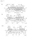
- Fig. 2 is a plan view of one of the pixels extracted included therein.
- Figs. 3(A), 3(B) and 3(C) are cross-sectional views taken from line A-A', B-B', and C-C', respectively, in Fig. 2.
- the central portion of a transparent substrate 10 as a base is used as a display section 11.
- a data line driving circuit 3 for outputting image signals is provided on the ends of data lines sig
- a scanning line driving circuit 4 for outputting scanning signals is provided on the ends of scanning lines gate.
- an n-TFT and a p-TFT form a complementary TFT
- many complementary TFTs form a shift resistor circuit, a level shifter circuit, and an analog switch circuit.
- a plurality of scanning lines gate a plurality of data lines sig extending perpendicular to the extending direction of the scanning lines gate , and a plurality of pixels 7 formed in a matrix by the data lines sig and the scanning lines gate are provided on the transparent substrate 10.
- Each pixel 7 is provided with a conduction control circuit 50 for supplying scanning signals through a scanning line gate , and a thin film luminescent device 40 emitting light on the basis of image signals supplied from a data line sig through the conduction control circuit 50 .
- the conduction control circuit 50 includes a first TFT 20 for supplying a scanning signal to a gate electrode through a scanning line gate , a holding capacitor cap for holding an image signal supplied from a data line sig through the first TFT 20, and a second TFT 30 for supplying the image signal held in the holding capacitor cap to the gate electrode.
- the second TFT 30 and the thin film luminescent device 40 are connected in series between an opposite electrode op and a common feed line com.
- the holding capacitor cap may be formed between the opposite electrode op and the scanning line gate , in addition to between the opposite electrode op and the common feed line com.
- the first TFT 20 and the second TFT 30 are formed using islands of semiconductive films (silicon films).
- a gate electrode 21 is formed as a part of the scanning line gate .
- one of the source and drain regions is electrically connected to the data line sig via a contact hole in a first insulating film 51, whereas the other is electrically connected to a drain electrode 22.
- the drain electrode 22 extends towards the region of the second TFT 30, and the extended section is electrically connected to a gate electrode 31 of the second TFT 30 via a contact hole in the first insulating film 51.
- One of the source and drain regions of the second TFT 30 is electrically connected to a relay electrode 35 simultaneously formed with the data line sig via a contact hole in the first insulating film 51, and the relay electrode 35 is electrically connected to a transparent pixel electrode 41 composed of an indium tin oxide (ITO) film in the thin film luminescent device 40 via a contact hole in a second insulating film 52.
- ITO indium tin oxide
- pixel electrodes 41 are independently formed in individual pixels 7.
- An organic semiconductive film 43 composed of polyphenylene vinylene (PPV) or the like and an opposite electrode op composed of a metal film such as lithium-containing aluminum or calcium are deposited above each pixel electrode 41, in that order, to form a thin film luminescent device 40.
- a stripe organic semiconductive film 43 will be formed over a plurality of pixels 7 in some cases, as will be described below.
- the opposite electrode op is formed over the entire display section 11, other than the periphery of the region in which terminals 12 are formed.
- the terminals 12 include a terminal electrically connected to the opposite electrode op formed using a conduction (not shown in the drawing) which is simultaneously formed with the opposite electrode op .
- the configuration of the thin film luminescent device 40 may be a configuration provided with a positive hole injection layer having an increased luminescent efficiency (hole injection efficiency), or a configuration provided with a positive hole injection layer and an electron injection layer.
- the other of the source and drain regions of the second TFT 30 is electrically connected to the common feed line com via a contact hole of the first insulating film 51.
- the extension 39 of the common feed line com faces the extension 36 of the gate electrode 31 separated by the first insulating film 51 as a dielectric film to form a holding capacitor cap .
- a capacitor line formed parallel to the scanning line gate may be used for the formation of the holding capacitor cap .
- the holding capacitor cap may be formed of the drain region of the first TFT 20 and the gate electrode 31 of the second TFT 39.
- the luminescent device 40 emits light as an electroluminescent device or an LED device.
- an insulating film (a bank layer bank , the region shaded with lines slanting downward to the left or double slanting lines at a wide pitch) which is thicker than the organic semiconductive film 41 is provided along the data line sig and the scanning line gate , and the opposite electrode op is formed above the bank layer bank . Since the second insulating film 52 and the thick bank layer bank are disposed between the data line sig and the opposite electrode op , the parasitic capacitance formed in the data line sig is significantly reduced. Thus, the load on the driving circuits 3 and 4 can be reduced, resulting in lower electrical power consumption and improved display operation.
- the bank layer bank consists of a lower insulating layer 61 which is formed of an inorganic material such as a silicon oxide film or a silicon nitride film and is thicker than the organic semiconductive film 41, and an upper insulating layer 62 which is formed on the lower insulating layer 61 and is composed of an organic material such as a resist or a polyimide film.
- the thicknesses of the organic semiconductive film 41, the lower insulating layer 61, and the upper insulating layer 62 are in ranges of 0.05 ⁇ m to 0.2 ⁇ m, 0.2 ⁇ m to 1.0 ⁇ m, and 1 ⁇ m to 2 ⁇ m, respectively.
- the upper insulating layer 62 is formed of a resist or a polyimide film which facilitates formation of a thick film; hence, only the lower insulating layer 61 can be formed of an inorganic material. Since the entire bank layer bank is not formed of an inorganic material, the formation of the inorganic film by, for example, a PECVD process does not require a long time. Thus, productivity of the active matrix display device 1 is increased.
- the organic semiconductive film 41 comes into contact with the inorganic lower insulating layer 61, but not with the organic upper insulating layer 62.
- the organic semiconductive film 41 is, therefore, not damaged by the effects of the organic upper insulating layer 62, and the thin film luminescent device 40 does not have decreased luminescent efficiency nor decreased reliability.
- the bank layer bank is also formed in the peripheral region of the transparent substrate 10 (the exterior region of the display section 11); hence the data line driving circuit 3 and the scanning line driving circuit 4 are covered with the bank layer bank .
- the opposite electrode op must be formed at least in the display section 11, but is unnecessary in the driving circuit region. Since the opposite electrode op is generally formed by a mask sputtering process, an inaccurate alignment such as overlap of the opposite electrode op and the driving circuits may occur.
- the bank layer bank is disposed between the lead layer of the driving circuits and the opposite electrode op ; hence formation of parasitic capacitance in the driving circuits 3 and 4 is prevented even if the opposite electrode op overlaps the driving circuits. As a result, the load on the driving circuits 3 and 4 is reduced, consumption of electrical power is reduced, and high-speed display operation is achieved.
- the bank layer bank is also formed in the area, which overlaps the relay electrode 35 of the conduction control circuit 50, in the region for forming the pixel electrode 41.
- the organic semiconductive film 43 is, therefore, not formed in the area overlapping the relay electrode 35. Since the organic semiconductive film 43 is formed only at the flat section in the region for forming the pixel electrode 41, the resulting organic semiconductive film 43 has a constant thickness so that irregularities of display do not occur. If the organic semiconductive film 43 has a part having a lesser thickness, the driving current for the thin film luminescent device 40 is concentrated therein, resulting in decreased reliability of the thin film luminescent device 40. The uniform thickness in this embodiment does not cause such a problem.
- the organic semiconductive film 43 emits light by a driving current between the relay electrode 35 and the opposite electrode op ; however, the relay electrode 35 and the opposite electrode op inhibit emission of the light to the exterior, and the light does not contribute to display.
- the driving current flowing in the section which does not contribute to display is an unavailable current in view of the display.
- the bank layer bank is formed at the position in which an unavailable current will flow so as to prevent an unavailable current flowing in the common feed line com.
- the width of the common feed line com can be reduced.
- the luminescent area which contributes to improved display performance, such as luminance and contrast, can be increased.
- the bank layer bank When the bank layer bank is formed of a black resist, the bank layer bank functions as a black matrix which improves the quality of display, such as contrast.
- the opposite electrode op is formed on the entire pixel 7 at the front face of the transparent substrate 10; hence light reflected by the opposite electrode op causes decreased contrast.
- the bank layer bank for preventing the formation of the parasitic capacitance is formed of a black resist, the bank layer bank also functions as a black matrix which shades the light reflected by the opposite electrode op and contributes to high contrast.
- the layer can prevent bleeding of a discharged solution outside when the organic semiconductive film 43 is formed by discharging a liquid material (discharging solution) through an ink-jet head in the production process of the active matrix display device.
- the steps for making the first TFT 20 and the second TFT 30 on the transparent substrate 10 are substantially the same as the steps for making the active matrix substrate of the active matrix liquid crystal display device; hence only the outline thereof will be briefly described with reference to Figs. 3(A), 3(B), and 3(C).
- an underlying protective film (not shown in the drawing) composed of a silicon oxide film with a thickness of approximately 2,000 to 5,000 angstroms is formed, if necessary, on a transparent substrate 10 by a plasma enhanced CVD using tetraethoxysilane (TEOS) and gaseous oxygen as formation gases.
- TEOS tetraethoxysilane
- a semiconductive film composed of an amorphous silicon film with a thickness of approximately 300 to 700 angstroms is formed on the underlying protective film by a plasma enhanced CVD.
- the amorphous silicon semiconductive film is subjected to a crystallization step, such as a laser annealing step or a solid phase deposition step so that the semiconductive film is crystallized to form a polysilicon film.
- the semiconductive film is patterned to form islands of semiconductive films, and then a gate insulating film 57 composed of a silicon oxide or silicon nitride film with a thickness of approximately 600 to 1,500 angstroms is formed thereon by a plasma enhanced CVD using tetraethoxysilane (TEOS), gaseous oxygen and the like as formation gases.
- TEOS tetraethoxysilane
- a conductive film composed of a metal film, such as aluminum, tantalum, molybdenum, titanium, or tungsten, is formed by a sputtering process, and is patterned to form gate electrodes 21 and 31 and an extension 36 of the gate electrode 31 (a gate electrode forming step). This step also forms a scanning line gate.
- a metal film such as aluminum, tantalum, molybdenum, titanium, or tungsten
- a high concentration of phosphorus ions are implanted to form source and drain regions by self-alignment with respect to the gate electrodes 21 and 31.
- the section which is not doped with the impurity functions as a channel region.
- a data line sig, a drain electrode 22, a common feed line com, an extension 39 of the common feed line com, and a relay electrode 35 are formed.
- a first TFT 20, a second TFT 30, and a holding capacitor cap are formed.
- a second insulating interlayer 52 is formed and a contact hole is formed at the position corresponding to the relay electrode 35 of the insulating interlayer.
- An ITO film is formed on the entire second insulating interlayer 52 and is patterned, and then a pixel electrode 41 which is electrically connected to the source and drain regions of the second TFT 30 via the contact hole is formed in each pixel 7.
- An inorganic film (for forming a lower insulating layer 61) is formed on the front face of the second insulating film 52 by a PECVD process, and then a resist (upper insulating layer 62) is formed along the scanning line gate and the data line sig .
- the inorganic film is patterned through the resist as a mask to form a lower insulating layer 61. Since the lower insulating layer 61 is thin, overetching does not occur when the lower insulating layer 61 is formed by such a patterning process. Thus, the pixel electrode 41 is not damaged.
- the inorganic film forms the lower insulating layer 61 along the scanning line gate and the data line sig.
- a double-layered bank layer bank including the lower insulating layer 61 and the upper insulating layer 62 is formed.
- the resist section remaining along the data line sig has a large width so as to cover the common feed line com.
- a region for forming the organic semiconductive film 43 in the luminescent device 40 is surrounded with the bank layer bank .
- Organic semiconductive films 43 corresponding to R, G, and B are formed in regions in a matrix delimited by the bank layer bank by an ink-jet process.
- a liquid material (a precursor or a discharging solution) for forming the organic semiconductive film 43 is discharged in the inner region of the bank layer bank through an ink-jet head and fixed in the inner region of the bank layer bank to form the organic semiconductive film 43.
- the upper insulating layer 62 of the bank layer bank is composed of a resist or a polyimide film, it has water-repellent properties.
- the precursor of the organic semiconductive film 43 contains a hydrophilic solution; hence, the region for forming the organic semiconductive film 43 is surely defined by the bank layer bank . Since the solution does not bleed out of the adjacent pixels 7, the organic semiconductive film 43 can be formed only in the predetermined region.
- the bank layer must have a thickness of approximately 1 ⁇ m to 3 ⁇ m.
- the solvent in the precursor is removed by heat treatment at 100°C to 150°C.
- the thickness of the organic semiconductive film 43 in the inner region of the bank layer bank is fixed in a range of approximately 0.05 ⁇ m to 0.2 ⁇ m. The organic semiconductive film 43 no longer is in contact with the upper insulating layer 62.
- the bank layer bank When the bank layer bank has a height of 1 ⁇ m or more, the bank layer bank sufficiently functions as a barrier even if the bank layer bank does not have water-repellent properties.
- Such a thick bank layer bank can define the region for forming the organic semiconductive film 43 when the film is formed by a coating process in place of the ink-jet process.
- an opposite electrode op is formed on substantially the entire transparent substrate 10.
- organic semiconductive films 43 can be formed at predetermined positions corresponding to R, G, and B by an ink-jet process; hence a full color active matrix display device 1 can be made with high productivity.
- TFTs are also formed in the data line driving circuit 3 and the scanning line driving circuit 4 shown in Fig. 1, these TFTs can be formed by completely or partly employing the above steps for forming the TFT in the pixel 7.
- the TFTs in the driving circuits are also formed in the same interlayer in which TFTs for pixels 7 are formed.
- combinations of an n-type and an n-type, of a p-type and a p-type, and of an n-type and a p-type are allowable. Since all the combinations of TFTs can be produced by any well-known method, description thereof will be omitted.
- Figs. 4(A), 4(B) and 4(C) are cross-sectional views of an active matrix display device in accordance with this embodiment at positions corresponding to line A-A', B-B', and C-C', respectively, in Fig. 2.
- This embodiment has a basic configuration which is substantially the same as that of the first embodiment; hence, the same symbols are assigned for the same parts, without detailed description thereof. Since the region for forming the bank layer bank in the active matrix display device of this embodiment is the same as that in the first embodiment, Figs. 1 and 2 are also referred to in the following description.
- an insulating film (a bank layer bank , the region shaded with lines slanting downward to the left or double slanting lines at a wide pitch) which is thicker than an organic semiconductive film 41 is provided along the data line sig and a scanning line gate , and an opposite electrode op is formed above the bank layer bank .
- the bank layer bank consists of an inorganic lower insulating layer 61 such as a silicon oxide or silicon nitride film which is thicker than the organic semiconductive film 41, and an upper organic insulating film 62 such as a resist or a polyimide film formed on the lower insulating layer 61.
- an inorganic lower insulating layer 61 such as a silicon oxide or silicon nitride film which is thicker than the organic semiconductive film 41
- an upper organic insulating film 62 such as a resist or a polyimide film formed on the lower insulating layer 61.
- the upper organic insulating film 62 has a smaller width than that of the lower inorganic insulating film 61 and is formed on the inner region of the lower insulating layer 61.
- the overlapping width of the upper insulating layer 62 and the pixel electrode 41 is in a range of 1 ⁇ m to 3 ⁇ m
- a gap between an edge of the lower insulating layer 61 and the corresponding edge of the upper insulating layer 62 is in a range of 1 ⁇ m to 5 ⁇ m.
- the bank layer bank has a double-layered configuration in which the underlying insulating film 61 and the upper insulating layer 62 having different widths are deposited.
- the upper insulating layer 62 is formed of a resist or a polyimide film, which facilitates formation of a thick film, in such a double-layered configuration, and only the lower insulating layer 61 is composed of an inorganic material.
- the process, such as a PECVD process, for forming the inorganic film does not require a long deposition time, unlike the process for forming a thick bank layer bank which is entirely composed of an inorganic material.
- the active matrix display device 1 can be manufactured with high productivity.
- the organic semiconductive film 41 comes into contact with the lower insulating layer 61, but not with the upper insulating layer 62. Furthermore, the upper insulating layer 62 is formed on the inner portion of the lower insulating layer 61 to avoid the contact of the organic semiconductive film 43 with the upper insulating layer 62. Thus, the upper organic insulating film 62 does not cause deterioration of the organic semiconductive film 41 which would result in decreased luminescent efficiency and decreased reliability of the thin film luminescent device 40.
- Each pixel 7 is surrounded with the bank layer bank.
- Organic semiconductive films 43 can be formed in predetermined positions corresponding to R, G, and B by an ink-jet process; hence, a full color active matrix display device 1 can be manufactured with high productivity, as in the first embodiment.
- an inorganic film for forming a lower insulating layer 61
- the lower insulating layer 61 is formed along the scanning line gate and the data line sig , and then a resist used for the patterning is removed.
- a resist or a polyimide film with a thickness which is smaller than that of the lower insulating layer 61 is formed thereon as the upper insulating layer 62. Since the lower insulating layer 61 is thin, overetching does not occur when the lower insulating layer 61 is formed by patterning. Thus, the pixel electrode 41 is not damaged.
- An active matrix display device 1 in this embodiment has the same configuration as that in the second embodiment, but a material for the bank layer bank is different. Thus, the same symbols are assigned for the same parts, without detailed description thereof. Figs. 1, 2, and 4 are also referred to in the following description, as in the second embodiment.
- an insulating film (a bank layer bank , the region shaded with lines slanting downward to the left or double slanting lines at a wide pitch) which is thicker than an organic semiconductive film 41 is provided along the data line sig and a scanning line gate , and an opposite electrode op is formed above the bank layer bank .
- the bank layer bank consists of an inorganic lower insulating layer 61 such as a silicon nitride film which is thicker than the organic semiconductive film 41, and an upper inorganic insulating film 62 such as a silicon oxide film formed on the lower insulating layer 61. Since the organic semiconductive film 43 does not come into contact with any other organic material in such a double-layered configuration, it will not be deteriorate by the effects of the other organic material. Thus, a decrease in luminescent efficiency and reliability does not occur in the thin film luminescent device 40.
- the upper organic insulating film 62 has a smaller width than that of the lower inorganic insulating film 61 and is formed on the inner region of the lower insulating layer 61.
- the bank layer bank has a double-layered configuration in which the underlying insulating film 61 and the upper insulating layer 62 having different widths are deposited.
- inorganic films for forming the lower insulating layer 61 and the upper insulating layer 62 are formed in that order, and the upper insulating layer 62 is patterned. Since the lower insulating layer 61 functions as an etching stopper, slight overetching will not damage the pixel electrode 41. After the patterning, the lower insulating layer 61 is patterned. Since a single layer of the lower insulating layer 61 is etched, the etching is readily controlled and overetching which would damage the pixel electrode 41 does not occur.
- Each pixel 7 is, therefore, surrounded with the bank layer bank .
- Organic semiconductive films 43 can be formed in predetermined positions corresponding to R, G, and B by an ink-jet process; hence, a full color active matrix display device 1 can be manufactured with high productivity, as in the first embodiment.
- the bank layer bank delimits pixels 7 in a matrix.
- the bank layer bank may be formed along only the data line sig .
- Organic semiconductive film 43 having a striped pattern, corresponding to R, G, and B, can be formed in striped regions delimited by the bank layer bank by an ink-jet process; hence a full color active matrix display device 1 can be made with high productivity.
- the corners delimited by the bank layer bank are edged in the above embodiments, it may be rounded so that the organic semiconductive film 43 has a rounded planar shape.
- the organic semiconductive film 43 having such a shape avoids the concentration of the driving current at the corners, hence defects, such as insufficient voltage resistance, can be prevented at the corners.
- An active matrix display device 1 in this embodiment has a basic configuration like that in the first, second or third embodiment; hence, Fig. 1 is referred to for the description, and the same symbols are assigned for the same parts, without detailed description thereof.
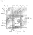
- Fig. 5 is a plan view of a pixel taken from an active matrix display device of this embodiment.
- Figs. 6(A), 6(B) and 6(C) are cross-sectional views taken from line A-A', B-B', and C-C', respectively, in Fig. 5.
- an upper insulating layer 62 partly overlaps a lower insulating layer 61 in this embodiment so that these films have different functions.
- a plurality of scanning lines gate a plurality of data lines sig extending perpendicular to the extending direction of the scanning lines gate, a plurality of common feed lines com formed parallel to the data lines sig, and a plurality of pixels 7 formed in a matrix by the data lines sig and the scanning lines gate are provided.
- a lower insulating layer 61 (a region shaded by double lines slanting down toward the left) is formed so as to cover an area overlapping the portion for forming a conduction control circuit 50 in the region for forming a pixel electrode 41; the data line sig; the common feed line com; and the scanning line gate .
- the upper insulating layer 62 (a region shaded by lines at a wide pitch and slanting down toward the left) is formed only on areas along the data lines sig in the region for forming the lower insulating layer 61 so as to form a striped pattern.
- Organic semiconductive films 43 are formed in the striped areas delimited by the upper insulating layer 62.
- the overlapping section of the lower insulating layer 61 and the upper insulating layer 62 is used as a bank layer bank to prevent bleeding of the discharged solution.
- the overlapping section of the lower insulating layer 61 and the upper insulating layer 62 has a thickness of 1 ⁇ m or more.
- the second insulating film 52 and the thick bank layer bank are disposed between the data lines sig and the opposite electrode op in such a configuration, parasitic capacitance forming in the data line sig is significantly reduced.
- the load on the driving circuits 3 and 4 can be reduced, resulting in lower electrical power consumption and improved display operation.
- the striped organic semiconductive films 43 are formed, an area overlapping the portion for forming a conduction control circuit 50 in the region for forming the pixel electrode 41, and a scanning line gate are covered with the upper insulating layer 62.
- organic semiconductive film 43 formed only on the flat section in the pixel electrode 41 contributes to luminescence.
- the thin film luminescent device 40 is formed only in the flat section of the pixel electrode 41.
- the organic semiconductive film 43 has a constant thickness and does not cause irregularities of display and concentration of a driving current. Since the lower insulating layer 61 inhibits a current flow in the section which does not contribute to display, an unavailable current does not flow in the common feed line com.
- the underlying insulating film 61 is formed of an inorganic material such as a silicon oxide film or a silicon nitride film which is thicker than the organic semiconductive film 41 and when the upper insulating layer 62 is composed of an organic material such as a resist or a polyimide film, only the lower insulating layer 61 is composed of the inorganic material.
- the process, such as a PECVD process, for forming the inorganic film does not require a long deposition time, unlike the process for forming a thick bank layer bank which is entirely composed of an inorganic material.
- the active matrix display device 1 can be manufactured with high productivity.
- the organic semiconductive film 41 comes into contact with the lower insulating layer 61, but not with the upper organic insulating film 62.
- the upper organic insulating film 62 does not cause deterioration of the organic semiconductive film 41 which results in decreased luminescent efficiency and decreased reliability of the thin film luminescent device 40.
- the organic semiconductive film 43 does not come into contact with an organic material and thus is not deteriorated by the effects of the organic material. Thus, a decrease in the luminescent efficiency and reliability does not occur in the thin film luminescent device 40.
- the lower insulating layer 61 functions as an etching stopper when the upper insulating layer 62 is patterned, as described in the third embodiment.
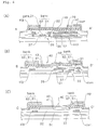
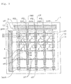
- Fig. 7 is a schematic block diagram of an overall layout of an active matrix display device.
- Fig. 8 is a plan view of a pixel extracted therefrom.
- Figs. 9(A), 9(B) and 9(C) are cross-sectional views taken from line A-A', B-B', and C-C', respectively, in Fig. 8.
- This embodiment has a basic configuration which is substantially the same as that of the first embodiment; hence, the same symbols are assigned for the same parts, without detailed description thereof.
- an insulating film (a bank layer bank , the region shaded with lines slanting downward to the left or double slanting lines at a wide pitch) which is thicker than an organic semiconductive film 41 is provided along the data line sig and a scanning line gate , and an opposite electrode op is formed above the bank layer bank . Since the second insulating film 52 and the thick bank layer bank are disposed between the data lines sig and the opposite electrode op , parasitic capacitance forming in the data line sig is significantly reduced. Thus, the load on the driving circuits 3 and 4 can be reduced, resulting in lower electrical power consumption and improved display operation.
- the bank layer bank consists of a lower insulating layer 61 which is formed of an inorganic material such as a silicon oxide film or a silicon nitride film and is thicker than the organic semiconductive film 41, and an upper insulating layer 62 which is formed on the lower insulating layer 61 and is composed of an organic material such as a resist or a polyimide film.
- the thicknesses of the organic semiconductive film 41, the lower insulating layer 61, and the upper insulating layer 62 are in ranges of 0.05 ⁇ m to 0.2 ⁇ m, 0.2 ⁇ m to 1.0 ⁇ m, and 1 ⁇ m to 2 ⁇ m, respectively.
- the organic semiconductive film 41 comes into contact with the inorganic lower insulating layer 61, but not with the organic upper insulating layer 62.
- the organic semiconductive film 41 is, therefore, not damaged by the effects of the organic upper insulating layer 62, and the thin film luminescent device 40, as in the first embodiment, does not have decreased luminescent efficiency nor decreased reliability.
- discontinuities portion off are provided for both the lower insulating layer 61 and the upper insulating layer 62 of the bank layer bank along the data lines sig between adjacent pixels 7.
- discontinuities portion off are also provided for both the lower insulating layer 61 and the upper insulating layer 62 of the bank layer bank along the scanning lines gate between adjacent pixels 7.
- discontinuities portion off are provided for both the lower insulating layer 61 and the upper insulating layer 62 of the bank layer bank at the ends of each data line sig and each scanning line gate.
- the thick bank layer bank is not provided at each discontinuity off , the discontinuity off does not have a large step and is flat. Thus, the opposite electrode op formed at this section does not cause disconnection.
- the opposite electrodes op of adjacent pixels 7 are securely connected through the flat section not having a step of the bank layer bank . Accordingly, a thick insulating film (a bank layer bank ) can be formed around a pixel 7 to suppress the parasitic capacitance, without disconnection of the opposite electrodes op formed on the thick insulating film (bank layer bank ).
- the data line driving circuit 3 and the scanning line driving circuit 4 are covered with the bank layer bank (the region is indicated by shading).
- the opposite electrode op provided above the region for forming these driving circuits is separated by the bank layer bank from the lead layer of these driving circuits. Since formation of the parasitic capacitance in the driving circuits can be prevented, the load on the driving circuits 3 and 4 can be reduced, resulting in lower electrical power consumption and improved display operation.
- a discontinuity off (second discontinuity) is provided for both the lower insulating layer 61 and the upper insulating layer 62 of the bank layer bank between the region for forming the scanning line driving circuit 4 and the region for the data line driving circuit 3.
- the opposite electrode op at the side of the display section 11 and the opposite electrode op at the peripheral side of the substrate are connected through the discontinuity off of the bank layer bank, and the discontinuity off is also a flat section not having a step. Since the opposite electrode op formed at the discontinuity off does not cause disconnection, the opposite electrodes op of the display section 11 and the opposite electrode op of the peripheral section of the substrate are securely connected through the discontinuity off of the bank layer bank . Thus, terminals 12 connected to the opposite electrode op of the peripheral section of the substrate are securely connected to the opposite electrode op of the display section 11.
- the bank layer bank is also formed in an area in which the region for forming the pixel electrode 41 overlaps the relay electrode 35 of the conduction control circuit 50 in this embodiment, no unavailable current flows. Accordingly, the width of the common feed line com can be reduced.
- the bank layer bank is formed on the front face of the second insulating film 52 along the scanning lines gate and the data lines sig, as in the first embodiment. Discontinuities portion off are formed at predetermined positions of the bank layer bank.
- the bank layer bank formed along the data lines sig has a larger width so that it can cover the common feed line com. As a result, the region for forming the organic semiconductive film 43 in the thin film luminescent device 40 is surrounded with the bank layer bank .
- Organic semiconductive films 43 corresponding to R, G, and B are formed in a region delimited as a matrix by the bank layer bank by an ink-jet process.
- a liquid material (a precursor) for forming the organic semiconductive film 43 is discharged into the inner region of the bank layer bank through an ink-jet head and is fixed in the inner region of the bank layer bank to form the organic semiconductive film 43.
- the upper insulating layer 62 of the bank layer bank is composed of a resist or a polyimide film, it has water-repellent properties.
- the precursor of the organic semiconductive film 43 contains a hydrophilic solution; hence, the region for forming the organic semiconductive film 43 is surely defined by the bank layer bank , and the solution does not bleed out of the adjacent pixels 7.
- the region for forming the organic semiconductive film 43 can be surely defined by the bank layer bank , and the solution does not bleed out into adjacent pixels 7. Accordingly, the organic semiconductive film 43 can be formed within a predetermined region.
- the bank layer Since the precursor discharged from the ink-jet head forms a convex surface with a thickness of approximately 2 ⁇ m to 4 ⁇ m by surface tension, the bank layer must have a thickness of approximately 1 ⁇ m to 3 ⁇ m. Although the precursor discharged from the ink-jet head comes into contact with the upper insulating layer 62 in this state, the solvent in the precursor is removed by heat treatment at 100°C to 150°C. Thus, the thickness of the organic semiconductive film 43 fixed in the inner region of the bank layer bank is in a range of approximately 0.05 ⁇ m to 0.2 ⁇ m. The organic semiconductive film 43 no longer is in contact with the upper insulating layer 62.
- the bank layer bank When the bank layer bank has a height of 1 ⁇ m or more, the bank layer bank sufficiently functions as a barrier even if the bank layer bank does not have water-repellent properties.
- Such a thick bank layer bank can define the region for forming the organic semiconductive film 43 when the film is formed by a coating process in place of the ink-jet process.
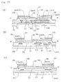
- Fig. 10 is a schematic block diagram of an overall layout of an active matrix display device.
- Fig. 11 is a plan view of a pixel taken from the device.
- Figs. 12(A), 12(B) and 12(C) are cross-sectional views taken from line A-A', B-B', and C-C', respectively, in Fig. 11.
- This embodiment has a basic configuration which is substantially the same as that of the first embodiment; hence, the same symbols are assigned for the same parts, without detailed description thereof.
- an insulating film (a bank layer bank , the region shaded with lines slanting downward to the left or double slanting lines at a wide pitch) which is thicker than an organic semiconductive film 43 is provided along the data line sig and a scanning line gate , and an opposite electrode op is formed above the bank layer bank . Since the second insulating film 52 and the thick bank layer bank are disposed between the data lines sig and the opposite electrode op, parasitic capacitance forming in the data line sig is significantly reduced. Thus, the load on the driving circuits 3 and 4 can be reduced, resulting in lower electrical power consumption and improved display operation.
- the bank layer bank consists of a lower insulating layer 61 which is formed of an inorganic material such as a silicon oxide film or a silicon nitride film and is thicker than the organic semiconductive film 43, and an upper insulating layer 62 which is formed on the lower insulating layer 61 and is composed of an organic material such as a resist or a polyimide film.
- the organic semiconductive film 43 comes into contact with the inorganic lower insulating layer 61, but not with the organic upper insulating layer 62.
- the organic semiconductive film 43 is, therefore, not damaged by the effects of the organic upper insulating layer 62, and the thin film luminescent device 40, as in the first embodiment, does not decreased luminescent efficiency nor decreased reliability.
- the bank layer bank is formed along the data line sig and the scanning line gate and each pixel 7 is surrounded with the bank layer bank .
- Organic semiconductive films 43 can be formed in predetermined positions corresponding to R, G, and B by an ink-jet process; hence, a full color active matrix display device 1 can be manufactured with high productivity.
- discontinuities portion off are provided for the bank layer bank along the scanning line gate between adjacent pixels 7.
- discontinuities portion off are also provided for the bank layer bank at the ends of each data line sig and each scanning line gate .
- a discontinuity off is provided for the bank layer bank between the region for forming the scanning line driving circuit 4 and the region for the data line driving circuit 3.
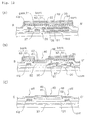
- Fig. 13 is a schematic block diagram of an overall layout of an active matrix display device.
- Fig. 14 is a plan view of a pixel taken from the device.
- Figs. 15(A), 15(B) and 15(C) are cross-sectional views taken from line A-A', B-B', and C-C', respectively, in Fig. 14.
- This embodiment has a basic configuration which is substantially the same as that of the first embodiment; hence, the same symbols are assigned for the same parts, without detailed description thereof.
- an insulating film (a bank layer bank , the region shaded with lines slanting downward to the left or double slanting lines at a wide pitch) which is thicker than an organic semiconductive film 43 is provided along the data line sig and a scanning line gate, and an opposite electrode op is formed above the bank layer bank . Since the second insulating film 52 and the thick bank layer bank are disposed between the data lines sig and the opposite electrode op , parasitic capacitance forming in the data line sig is significantly reduced. Thus, the load on the driving circuits 3 and 4 can be reduced, resulting in lower electrical power consumption and improved display operation.
- the bank layer bank consists of a lower insulating layer 61 which is formed of an inorganic material such as a silicon oxide film or a silicon nitride film and is thicker than the organic semiconductive film 43, and an upper insulating layer 62 which is formed on the lower insulating layer 61 and is composed of an organic material such as a resist or a polyimide film.
- the organic semiconductive film 43 comes into contact with the inorganic lower insulating layer 61, but not with the organic upper insulating layer 62.
- the organic semiconductive film 43 is, therefore, not damaged by the effects of the organic upper insulating layer 62, and the thin film luminescent device 40, as in the first embodiment, does not have decreased luminescent efficiency nor decreased reliability.
- the bank layer bank is formed along the data line sig and the scanning line gate and each pixel 7 is surrounded with the bank layer bank.
- Organic semiconductive films 43 can be formed in predetermined positions corresponding to R, G, and B by an ink-jet process; hence, a full color active matrix display device 1 can be manufactured with high productivity.
- discontinuities portion off are provided for the bank layer bank along the data line sig between adjacent pixels 7.
- discontinuities portion off are also provided for the bank layer bank at the ends of each data line sig and each scanning line gate.
- a discontinuity off is provided for the bank layer bank between the region for forming the scanning line driving circuit 4 and the region for the data line driving circuit 3.
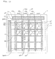
- Fig. 16 is a schematic block diagram of an overall layout of an active matrix display device.
- Fig. 17 is a plan view of a pixel taken from the device.
- Figs. 18(A), 18(B), and 18(C) are cross-sectional views taken from line A-A', B-B', and C-C', respectively, in Fig. 17.
- This embodiment has a basic configuration which is substantially the same as that of the first and fifth embodiments; hence, the same symbols are assigned for the same parts, without detailed description thereof.
- an insulating film (a bank layer bank, the region shaded with lines slanting downward to the left or double slanting lines at a wide pitch) which is thicker than an organic semiconductive film 43 is provided along the data line sig and a scanning line gate, and an opposite electrode op is formed above the bank layer bank. Since the second insulating film 52 and the thick bank layer bank are disposed between the data lines sig and the opposite electrode op , parasitic capacitance forming in the data line sig is significantly reduced. Thus, the load on the driving circuits 3 and 4 can be reduced, resulting in lower electrical power consumption and improved display operation.
- the bank layer bank consists of a lower insulating layer 61 which is formed of an inorganic material such as a silicon oxide film or a silicon nitride film and is thicker than the organic semiconductive film 43, and an upper insulating layer 62 which is formed on the lower insulating layer 61 and is composed of an organic material such as a resist or a polyimide film.
- the bank layer bank is formed along the data line sig and the scanning line gate and each pixel 7 is surrounded with the bank layer bank .
- Organic semiconductive films 43 can be formed in predetermined positions corresponding to R, G, and B by an ink-jet process; hence, a full color active matrix display device 1 can be manufactured with high productivity.
- discontinuities portion off are provided for the bank layer bank along the data line sig between adjacent pixels 7.
- discontinuities portion off are also provided for the bank layer bank at the ends of each data line sig and each scanning line gate .
- a discontinuity off is provided for the bank layer bank between the region for forming the scanning line driving circuit 4 and the region for the data line driving circuit 3.
- these discontinuities portion off are provided for only the upper insulating layer 62 between the lower insulating layer 61 (a region shaded by double slashes) and the upper insulating layer 62 (a region shaded by lines slanting down to the left) of the bank layer bank , and thus the lower insulating layer 61 is formed at the discontinuities portion off .
- the lower insulating layer 61 is formed for the first and second discontinuities portion in this embodiment, the present invention is not limited to this embodiment.
- the lower insulating layer 61 may be formed for either the first discontinuities portion or the second discontinuity.
- the configuration of this embodiment in which the lower insulating layer 61 is formed at the discontinuities portion can be applied to the bank layer bank having a pattern described in any other embodiment.
- Fig. 19 is a schematic block diagram of an overall layout of an active matrix display device.
- Fig. 20 is a plan view of a pixel taken from the device.
- Figs. 21(A), 21(B) and 21(C) are cross-sectional views taken from line A-A', B-B', and C-C', respectively, in Fig. 20.
- This embodiment has a basic configuration which is substantially the same as that of the first and fifth embodiments; hence, the same symbols are assigned for the same parts, without detailed description thereof.
- an insulating film (a bank layer bank , the region shaded with lines slanting downward to the left or double slanting lines at a wide pitch) which is thicker than an organic semiconductive film 43 is provided along the data line sig and a scanning line gate , and an opposite electrode op is formed above the bank layer bank . Since the second insulating film 52 and the thick bank layer bank are disposed between the data lines sig and the opposite electrode op , parasitic capacitance forming in the data line sig is significantly reduced. Thus, the load on the driving circuits 3 and 4 can be reduced, resulting in lower electrical power consumption and improved display operation.
- the bank layer bank consists of a lower insulating layer 61 which is formed of an inorganic material such as a silicon oxide film or a silicon nitride film and is thicker than the organic semiconductive film 43, and an upper insulating layer 62 which is formed on the lower insulating layer 61 and is composed of an organic material such as a resist or a polyimide film.
- the organic semiconductive film 43 comes into contact with the inorganic lower insulating layer 61, but not with the organic upper insulating layer 62.
- the organic semiconductive film 43 is, therefore, not damaged by the effects of the organic upper insulating layer 62, and the thin film luminescent device 40 does not have decreased luminescent efficiency nor decreased reliability.
- organic semiconductive film 43 having a striped pattern, corresponding to R, G, and B, can be formed in striped regions delimited by the bank layer bank by an ink-jet process; hence a full color active matrix display device 1 can be made with high productivity.
- discontinuities portion off are provided for both the lower insulating layer 61 and the upper insulating layer 62 of the bank layer bank along the data lines sig at the ends of each data line sig .
- the opposite electrode op of each pixel 7 is connected to the opposite electrode op of the adjacent pixel 7 over the thick bank layer bank in the direction of the scanning line gate .
- the opposite electrode op of each pixel 7 is connected to the opposite electrode op of the adjacent pixel 7 at the discontinuity off (the flat section not having a step due to the bank layer bank ) at the ends of the data line sig . Since the opposite electrode op of each pixel 7 is connected to the opposite electrode op of the adjacent pixel 7 at the flat section not having a step due to the bank layer bank , the opposite electrode op of each pixel 7 does not cause disconnection.
- the data line driving circuit 3 and the scanning line driving circuit 4 are covered with the bank layer bank.
- the opposite electrode op provided above the region for forming these driving circuits is separated by the bank layer bank from the lead layer of these driving circuits. Since formation of the parasitic capacitance in the driving circuits can be prevented, the load on the driving circuits 3 and 4 can be reduced, resulting in lower electrical power consumption and improved display operation.
- the bank layer bank which is formed above the scanning line driving circuit 4 and the data line driving circuit 3, has a discontinuity off (second discontinuity) between the region for forming the scanning line driving circuit 4 and the region for the data line driving circuit 3.
- the opposite electrodes are securely connected through the flat section not having a step due to the bank layer bank (the discontinuity off ) without disconnection.
- the configuration in which only the upper insulating layer 62 has discontinuities portion off of the bank layer bank may also be applied to the sixth embodiment
- the concept of provision of discontinuities portion off in the bank layer bank for avoiding disconnection of the opposite electrodes op is also applicable to a bank layer bank composed of an inorganic material, as described in the third embodiment.
- the insulating film which is formed so as to surround the region for forming the organic semiconductive film consists of a lower insulating layer which is composed of an inorganic material and is thicker than the organic semiconductive film, and an upper insulating layer which is formed thereon and is composed of an organic material. Since a thick insulating film is disposed between the data line and the opposite electrode, formation of parasitic capacitance in the data line can be prevented. Thus, the load on the data line driving circuit can be reduced, resulting in lower electrical power consumption and improved display operation.
- the process has high productivity.
- the upper insulating layer does not come into contact with the organic semiconductive film, but the lower insulating layer composed of an inorganic material does come into contact with the organic semiconductive film; hence, the organic semiconductive film is protected from deterioration caused by the upper insulating layer. Accordingly, the thin film luminescent device does not have decreased luminescent efficiency or reliability.
- the insulating film formed so as to surround the region for forming the organic semiconductive film consists of a lower insulating layer composed of an inorganic material and an upper insulating layer which is formed on an inner region of the lower insulating layer and has a smaller width than that of the lower insulating layer.
- the thick insulating film disposed between the data line and the opposite electrode can prevent formation of parasitic capacitance in the data line.
- the load on the data line driving circuit can be reduced, resulting in lower electrical power consumption and improved display operation.
- the lower insulating layer functions as an etching stopper.
Abstract
Description
- The present invention relates to active matrix display devices which control thin film luminescent devices, such as electroluminescent (EL) devices emitting light by a driving current flowing in an organic semiconductive film, and light-emitting diode (LED) devices using thin film transistors (hereinafter referred to as TFTs).
- Active matrix display devices using current-control-type luminescent devices, such as EL devices or LED devices have been proposed. Since luminescent devices used in such types of display devices have self-luminescent functions; these have advantages, such as no installation of a backlight being necessary, whereas backlights are essential for liquid crystal display devices, and a wider viewing angle.
- Fig. 22 is a block diagram of an active matrix display device using charge-injection-type organic EL devices. In the active matrix display device 1A shown in the drawing, a plurality of scanning lines gate, a plurality of data lines sig extending in the direction perpendicular to the direction of the scanning lines gate, a plurality of common feed lines com along the data lines sig, and a plurality of
pixels 7 in a matrix formed by the data lines sig and the scanning lines gate are formed on atransparent substrate 10. A dataline driving circuit 3 and a scanningline driving circuit 4 are provided for the data lines sig and the scanning lines gate, respectively. Eachpixel 7 is provided with aconduction control circuit 50 for supplying scanning signals from a scanning line gate, and a thin filmluminescent device 40 emitting light based on image signals supplied from a data line sig through theconduction control circuit 50. In this example, theconduction control circuit 50 has afirst TFT 20 for supplying scanning signals from the scanning line gate to a gate electrode; a holding capacitor cap for holding image signals supplied from the data line sig through thefirst TFT 20; and asecond TFT 30 for supplying the image signals held in the holding capacitor cap to the gate electrode. Thesecond TFT 30 and the thin filmluminescent device 40 are connected in series between an opposite electrode op (described below) and a common feed line com. The thin filmluminescent device 40 emits light by a driving current from the common feed line com when thesecond TFT 30 is an ON mode, and this emitting mode is maintained by a holding capacitor cap for a predetermined time. - In such a configuration of active matrix display device 1A, as shown in Figs. 23, 24(A), and 24(B), the
first TFT 20 and thesecond TFT 30 are formed of islands of a semiconductive film in eachpixel 7. The first TFT 20 is provided with agate electrode 21 as a part of a scanning line gate. In thefirst TFT 20, one source-drain region is electrically connected to a data line sig through a contact hole in a firstinsulating interlayer 51, and the other region is connected to adrain electrode 22. Thedrain electrode 22 extends towards the region of thesecond TFT 30, and this extension is electrically connected to agate electrode 31 of thesecond TFT 30 through a contact hole in the firstinsulating interlayer 51. One source-drain region of thesecond TFT 30 is electrically connected to arelay electrode 35 through a contact hole of the firstinsulating interlayer 51, and therelay electrode 35 is electrically connected to apixel electrode 41 of the thin filmluminescent device 40 through a contact hole in a secondinsulating interlayer 52. - Each
pixel electrode 41 is independently formed in eachpixel 7, as shown in Figs. 23, 24(B), and 24(C). An organicsemiconductive film 43 and an opposite electrode op are formed above thepixel electrode 41 in that order. Although the organicsemiconductive film 43 is formed in eachpixel 7, a stripe film may be formed over a plurality ofpixels 7. The opposite electrode op is formed not only in adisplay section 11 includingpixels 7, but also over the entire surface of thetransparent substrate 10. - With reference to Figs. 23 and 24(A) again, the other source-drain region of the
second TFT 30 is electrically connected to the common feed line com through a contact hole in the firstinsulating interlayer 51. Anextension 39 of the common feed line com faces anextension 36 of thegate electrode 31 in thesecond TFT 30 separated by the firstinsulating interlayer 51 as a dielectric film to form a holding capacitor cap. - In the active matrix display device 1A, however, only the second
insulating interlayer 52 is disposed between the opposite electrode op facing thepixel electrode 41 and the data line sig on the sametransparent substrate 10, unlike liquid crystal active matrix display devices; hence, a large capacitance is formed in the data line sig and the dataline driving circuit 3 is heavily loaded. - Accordingly, as shown in Figs. 22, 23, 25(A), 25(B), and 25(C), the present inventors propose a reduction in parasitic capacitance in the data line sig by providing a thick insulating film (a bank layer bank; the region shaded with lines slanting downward to the left at a wide pitch) between the opposite electrode op and the data line sig. Furthermore, the present inventors propose that the region for forming the organic
semiconductive film 43 be surrounded with the insulating film (bank layer bank) to contain any solution discharged from an ink-jet head and to prevent bleeding of the solution towards the sides during formation of the organicsemiconductive film 43. - When the entire bank layer bank is formed of a thick inorganic material in adoption of such a configuration, a problem of a prolonged film forming time arises. When the thick inorganic film is patterned, the
pixel electrode 41 may be damaged due to overetching. On the other hand, when the bank layer bank is formed of an organic material, such as a resist, the organicsemiconductive film 43 may deteriorate at the boundary between the organicsemiconductive film 43 and the bank layer bank by the effects of the solvent components contained in the organic material in the bank layer bank. - Since formation of a thick bank layer bank causes formation of a large step difference bb, the opposite electrode op formed above the bank layer bank readily breaks on the step difference bb. Such breakage of the opposite electrode op due to the step difference bb causes insulation of the opposite electrode op from the neighboring opposite electrodes op to form point or linear defects in the display. When the opposite electrode op breaks along the outer periphery of the bank layer bank which covers the surfaces of the data
line driving circuit 3 and the scanningline driving circuit 4, the opposite electrode op in thedisplay section 11 is completely insulated from aterminal 12 and thus no image is displayed. - Accordingly, it is an object of the present invention in view of the above problems to provide an active matrix display device, without damage of thin film luminescent devices, having a thick insulating film satisfactorily formed around an organic semiconductive film in the thin film luminescent devices.
- It is another object of the present invention to provide an active matrix display device without breakage of an opposite electrode formed on a thick insulating film which is formed around an organic semiconductive film to reduce parasitic capacitance.
- The present invention for solving the above-mentioned problems is characterized by an active matrix display device comprising a display region including a plurality of scanning lines on a substrate, a plurality of data lines extending in the direction perpendicular to the direction of the scanning lines, and a plurality of pixels arranged in a matrix delimited by the data lines and the scanning lines; each of the pixels being provided with a thin film luminescent device having a conduction control circuit containing a thin film transistor for supplying a scanning signal to a gate electrode through one of the scanning lines, a pixel electrode, an organic semiconductive film deposited above the pixel electrode, and an opposite electrode deposited above the organic semiconductive film; the thin film luminescent device emitting light based on an image signal supplied from the data line through the conduction control circuit; wherein the region for forming the organic semiconductive film is divided by an insulating film which is thicker than the organic semiconductive film; and the insulating film comprises a lower insulating layer which is formed of an inorganic material and is thicker than the organic semiconductive film, and an upper insulating layer which is deposited on the lower insulating layer and is formed of an organic material.
- In the present invention, the data line will form large parasitic capacitance if the opposite electrode is formed on the entire surface of the display section to face the data line; however, a thick insulating film is provided between the data line and the opposite electrode in the present invention to prevent formation of the parasitic capacitance in the data line. As a result, a load on the data line driving circuit is reduced, and low energy consumption and high-speed display operation are achieved. If the thick insulating film is formed of only an inorganic material, a long film deposition time is required, resulting in low productivity. In the present invention, only the lower insulating layer in contact with the organic semiconductive film of the thin film luminescent device is formed of an inorganic material, and an upper insulating layer composed of an organic material such as a resist is formed thereon. Since the upper insulating layer composed of an organic material facilitates formation of a thick film and so results in improved productivity. The upper insulating layer does not come into contact with the organic semiconductive film, but the lower insulating layer composed of an inorganic material does come into contact with the organic semiconductive film; hence, the organic semiconductive film is protected from deterioration affected by the upper insulating layer. Accordingly, the thin film luminescent device does not have any decreased luminescent efficiency or reliability.
- It is preferable in the present invention that the upper insulating layer be deposited in an inner region of the lower insulating layer so as to have a width narrower than that of the upper insulating layer. Such a two-step configuration prevents contact of the upper insulating layer composed of an organic material with the organic semiconductive film; hence deterioration of the organic semiconductive film can be more securely prevented.
- In such a two-step configuration, both the lower insulating layer and the upper insulating layer may be formed of inorganic materials. Another aspect of the present invention is an active matrix display device comprising a display region including a plurality of scanning lines on a substrate, a plurality of data lines extending in the direction perpendicular to the direction of the scanning lines, and a plurality of pixels arranged in a matrix delimited by the data lines and the scanning lines; each of the pixels being provided with a thin film luminescent device having a conduction control circuit containing a thin film transistor for supplying a scanning signal to a gate electrode through one of the scanning lines, a pixel electrode, an organic semiconductive film deposited above the pixel electrode, and an opposite electrode deposited above the organic semiconductive film; the thin film luminescent device emitting light based on an image signal supplied from the data line through the conduction control circuit; wherein the region for forming the organic semiconductive film is divided by an insulating film which is thicker than the organic semiconductive film; and the insulating film comprises a lower insulating layer composed of an inorganic material, and an upper insulating layer, composed of an inorganic material, so as to have a width which is narrower than that of the lower insulating layer.
- In such a configuration, after films composed of inorganic materials, constituting a lower insulating layer and an upper insulating layer, are formed, the upper insulating layer is patterned. Since the lower insulating layer functions as an etching stopper, the pixel electrodes will not be damaged by slight overetching. After the patterning, the lower insulating layer is patterned. Since only one layer of the lower insulating layer is etched, the etching is readily controlled so that overetching, which would damage the pixel electrodes, does not occur.
- It is preferable in the present invention that the conduction control circuit be provided with a first TFT for supplying the scanning signal to the gate electrode and a second TFT of which the gate electrode is connected to the data line through the first TFT, and that the second TFT and the thin film luminescent device be connected in series between a common feed line formed in addition to the data line and the scanning line for supplying a drive current and the opposite electrode. Although the conduction control circuit can be composed of a TFT and a holding capacitor, the conduction control circuit of each pixel is preferably composed of two TFTs and two holding capacitors for improving display quality.
- It is preferable in the present invention that the insulating film be used as a bank layer which prevents bleeding of a discharged solution when the organic semiconductive film is formed by an ink-jet process in a region delimited by the insulating film. The insulating film preferably has a thickness of 1 µm or more.
- It is preferable in the present invention that a region overlapping the area for forming the conduction control circuit in the region for forming the pixel electrode be covered with the insulating film. That is, it is preferable that within the region for forming the pixel electrode, the thick insulating film be opened only at the flat section not having the conduction control circuit and the organic semiconductive film be formed only at the interior thereof. Such a configuration can prevent display irregularities due to an irregular thickness of the organic semiconductive film. A thinner section of the organic semiconductive film causes a concentration of the driving current of the thin film luminescent device and decreased reliability; however, this configuration can prevent such a problem. If the organic semiconductive film emits light due to a driving current between a pixel electrode and the opposite electrode in the region overlapping the conduction control circuit, the light is shaded by the conduction control circuit and does not contribute to display. The driving current not contributing to display by the shading effect of the conduction control circuit is an unavailable current. In the present invention, the thick insulating film is formed at the section, in which such an unavailable current is expected, to prevent formation of the unavailable current. As a result, a current in the common feed line can be reduced. Thus, by reducing the width of the common feed line, a luminescent area can be increased, improving display characteristics, such as luminance and contrast.
- In the present invention, the corners delimited by the insulating film may be rounded so that the organic semiconductive film has a rounded planar shape. The organic semiconductive film having such a shape avoids the concentration of the driving current at the corners, hence defects, such as insufficient voltage resistance, can be prevented at the corners.
- When the organic semiconductive film having a striped pattern is formed, the lower insulating layer of the insulating film is formed so as to cover the area for forming the conduction control circuit in the region for forming the pixel electrode, the data line, the common feed line, and the scanning line, whereas the upper insulating layer is formed so as to form a striped pattern along the data line, and the organic semiconductive film is formed in the region delimited by the striped pattern of the upper insulating layer by, for example, an ink-jet process.
- In such a configuration, the conduction control circuit is covered with the lower insulating layer so that only the organic semiconductive film formed at the flat section of the pixel electrode contributes to luminescence. That is, the thin film luminescent device is formed only at the flat section of the pixel electrode. Thus, the resulting organic semiconductive film has a constant thickness and does not display irregularities. Since the lower insulating layer prevents a driving current in the section not contributing to display, an unavailable current in the common feed line can be prevented. In such a configuration, the section in which the lower insulating layer overlaps the upper insulating layer can be used as a bank layer for preventing bleeding of a discharged solution when the organic semiconductive film is formed by an ink-jet process. When the insulating film is used as a bank layer, the overlapping section of the lower insulating layer and the upper insulating layer preferably has a thickness of 1 µm or more.
- It is preferable in the present invention that the insulating film have a first discontinuities portion so that opposite electrodes of adjacent pixels are connected to each other at flat sections formed by the first discontinuities portion. The thick insulating film in the present invention may form a large step which causes breakage of the opposite electrode formed thereon; however, the first discontinuities portion formed at predetermined positions of the thick insulating film are planarized. Since the opposite electrodes of individual regions are electrically connected to each other at the flat sections corresponding to the first discontinuities portion, the opposite electrodes are protected from breakage even if breakage occurs at the step due to the insulating film. Since breakage of the opposite electrode formed above the insulating film does not occur when a thick insulating film is formed around the organic semiconductive film to suppress the parasitic capacitance, display quality and reliability of the active matrix display device can be improved.
- When the insulating film is formed along the data line and the scanning line so as to surround the region for forming the organic semiconductive film, the first discontinuities portion are preferably formed between the adjacent pixels in the direction of the extending data line, between the adjacent pixels in the direction of the extending scanning line, or between the adjacent pixels in these directions.
- When the insulating film extends in a striped pattern along the data line, the first discontinuity may be formed on at least one end of the extending direction.
- It is preferable in the present invention that the periphery of the display section be provided with a data line driving circuit for supplying data signals through the data lines, and a scanning line driving circuit for supplying scanning signals through the scanning lines, that the insulating film be also formed above the scanning line driving circuit and the data line driving circuit, and that the insulating film have a second discontinuity at a position between the region for forming the scanning line driving circuit and the region for forming the data line driving circuit so that the opposite electrodes at the display section and at the peripheral section of the substrate are connected through the flat section. Even if breakage of the opposite electrodes occurs along the periphery of the insulating film which covers the data line driving circuit and the scanning line driving circuit, the opposite electrode at the display section is connected to the opposite electrode at the periphery of the substrate via the flat section, and thus electrical connection between these opposite electrodes can be ensured.
- In the discontinuity of the present invention, both the lower insulating layer and the upper insulating layer may have the discontinuity, or only the upper insulating layer between the upper insulating layer and the lower insulating layer may have the discontinuity.
-
- Fig. 1 is a schematic block diagram of an overall layout of an active matrix display device in accordance with a first embodiment of the present invention.
- Fig. 2 is a plan view of a pixel taken from the active matrix display device shown in Fig. 1.
- Figs. 3(A), 3(B) and 3(C) are cross-sectional views taken from line A-A', B-B', and C-C', respectively, in Fig. 2.
- Figs. 4(A), 4(B) and 4(C) are cross-sectional views of active matrix display devices in accordance with a second embodiment and a third embodiment of the present invention at positions corresponding to line A-A', B-B', and C-C', respectively, in Fig. 2.
- Fig. 5 is a plan view of a pixel taken from an active matrix display device in accordance with a fourth embodiment of the present invention.
- Figs. 6(A), 6(B) and 6(C) are cross-sectional views taken from line A-A', B-B', and C-C', respectively, in Fig. 5.
- Fig. 7 is a schematic block diagram of an overall layout of an active matrix display device in accordance with a fifth embodiment of the present invention.
- Fig. 8 is a plan view of a pixel taken from the active matrix display device shown in Fig. 7.
- Figs. 9(A), 9(B) and 9(C) are cross-sectional views taken from line A-A', B-B', and C-C', respectively, in Fig. 8.
- Fig. 10 is a schematic block diagram of an overall layout of an active matrix display device in accordance with a first modification of the fifth embodiment of the present invention.
- Fig. 11 is a plan view of a pixel taken from the active matrix display device shown in Fig. 10.
- Figs. 12(A), 12(B) and 12(C) are cross-sectional views taken from line A-A', B-B', and C-C', respectively, in Fig. 11.
- Fig. 13 is a schematic block diagram of an overall layout of an active matrix display device in accordance with a second modification of the fifth embodiment of the present invention.
- Fig. 14 is a plan view of a pixel taken from the active matrix display device shown in Fig. 13.
- Figs. 15(A), 15(B) and 15(C) are cross-sectional views taken from line A-A', B-B', and C-C', respectively, in Fig. 14.
- Fig. 16 is a schematic block diagram of an overall layout of an active matrix display device in accordance with a third modification of the fifth embodiment of the present invention.
- Fig. 17 is a plan view of a pixel taken from the active matrix display device shown in Fig. 16.
- Figs. 18(A), 18(B) and 18(C) are cross-sectional views taken from line A-A', B-B', and C-C', respectively, in Fig. 17.
- Fig. 19 is a schematic block diagram of an overall layout of an active matrix display device in accordance with a sixth embodiment of the present invention.
- Fig. 20 is a plan view of a pixel taken from the active matrix display device shown in Fig. 19.
- Figs. 21(A), 21(B) and 21(C) are cross-sectional views taken from line A-A', B-B', and C-C', respectively, in Fig. 20.
- Fig. 22 is a schematic block diagram of an overall layout of a conventional active matrix display device or an active matrix display device in accordance with a comparative embodiment of the present invention.
- Fig. 23 is a plan view of a pixel taken from the active matrix display device shown in Fig. 22.
- Figs. 24(A), 24(B) and 24(C) are cross-sectional views taken from line A-A', B-B', and C-C', respectively, in Fig. 23.
- Figs. 25(A), 25(B) and 25(C) are cross-sectional views of an active matrix display device in accordance with a comparative embodiment at positions corresponding to line A-A', B-B', and C-C', respectively, in Fig. 23.
-
-
- 1
- active matrix display device
- 2
- display section
- 3
- data line driving circuit
- 4
- scanning line driving circuit
- 7
- pixel
- 10
- transparent substrate
- 12
- terminal
- 20
- first TFT
- 21
- gate electrode of first TFT
- 30
- second TFT
- 31
- gate electrode of second TFT
- 40
- luminescent device
- 41
- pixel electrode
- 43
- organic semiconductive material
- 61
- lower insulating layer
- 62
- upper insulating layer
- bank
- bank layer (insulating film)
- cap
- holding capacitor
- com
- common feed line
- gate
- scanning line
- op
- opposite electrode
- off
- discontinuity of bank layer
- sig
- data line
- Embodiments of the present invention will now be described with reference to the drawings. Parts having the same functions as in Figs. 22 and 25 are referred to the same numerals.
- Fig. 1 is a schematic block diagram of an overall layout of an active matrix display device in accordance with the present invention. Fig. 2 is a plan view of one of the pixels extracted included therein. Figs. 3(A), 3(B) and 3(C) are cross-sectional views taken from line A-A', B-B', and C-C', respectively, in Fig. 2.
- In the active
matrix display device 1 shown in Fig. 1, the central portion of atransparent substrate 10 as a base is used as adisplay section 11. Within the peripheral section of thetransparent substrate 10, a dataline driving circuit 3 for outputting image signals is provided on the ends of data lines sig, whereas a scanningline driving circuit 4 for outputting scanning signals is provided on the ends of scanning lines gate. In these drivingcircuits display section 11, like in an active matrix substrate of an active matrix liquid crystal display device, a plurality of scanning lines gate, a plurality of data lines sig extending perpendicular to the extending direction of the scanning lines gate, and a plurality ofpixels 7 formed in a matrix by the data lines sig and the scanning lines gate are provided on thetransparent substrate 10. - Each
pixel 7 is provided with aconduction control circuit 50 for supplying scanning signals through a scanning line gate, and a thin filmluminescent device 40 emitting light on the basis of image signals supplied from a data line sig through theconduction control circuit 50. In this embodiment, theconduction control circuit 50 includes afirst TFT 20 for supplying a scanning signal to a gate electrode through a scanning line gate, a holding capacitor cap for holding an image signal supplied from a data line sig through thefirst TFT 20, and asecond TFT 30 for supplying the image signal held in the holding capacitor cap to the gate electrode. Thesecond TFT 30 and the thin filmluminescent device 40 are connected in series between an opposite electrode op and a common feed line com. The holding capacitor cap may be formed between the opposite electrode op and the scanning line gate, in addition to between the opposite electrode op and the common feed line com. - As shown in Figs. 2, 3(A), and 3(B), in each pixel of the active
matrix display device 1 having such a configuration, thefirst TFT 20 and thesecond TFT 30 are formed using islands of semiconductive films (silicon films). - In the
first TFT 20, agate electrode 21 is formed as a part of the scanning line gate. In thefirst TFT 20, one of the source and drain regions is electrically connected to the data line sig via a contact hole in a first insulatingfilm 51, whereas the other is electrically connected to adrain electrode 22. Thedrain electrode 22 extends towards the region of thesecond TFT 30, and the extended section is electrically connected to agate electrode 31 of thesecond TFT 30 via a contact hole in the first insulatingfilm 51. - One of the source and drain regions of the
second TFT 30 is electrically connected to arelay electrode 35 simultaneously formed with the data line sig via a contact hole in the first insulatingfilm 51, and therelay electrode 35 is electrically connected to atransparent pixel electrode 41 composed of an indium tin oxide (ITO) film in the thin filmluminescent device 40 via a contact hole in a second insulatingfilm 52. - As shown in Figs. 2, 3(B), and 3(C),
pixel electrodes 41 are independently formed inindividual pixels 7. An organicsemiconductive film 43 composed of polyphenylene vinylene (PPV) or the like and an opposite electrode op composed of a metal film such as lithium-containing aluminum or calcium are deposited above eachpixel electrode 41, in that order, to form a thin filmluminescent device 40. Although an organicsemiconductive film 43 is formed on each pixel in this embodiment, a stripeorganic semiconductive film 43 will be formed over a plurality ofpixels 7 in some cases, as will be described below. The opposite electrode op is formed over theentire display section 11, other than the periphery of the region in whichterminals 12 are formed. Theterminals 12 include a terminal electrically connected to the opposite electrode op formed using a conduction (not shown in the drawing) which is simultaneously formed with the opposite electrode op. - The configuration of the thin film
luminescent device 40 may be a configuration provided with a positive hole injection layer having an increased luminescent efficiency (hole injection efficiency), or a configuration provided with a positive hole injection layer and an electron injection layer. - With reference to Figs. 2 and 3(A) again, the other of the source and drain regions of the
second TFT 30 is electrically connected to the common feed line com via a contact hole of the first insulatingfilm 51. Theextension 39 of the common feed line com faces theextension 36 of thegate electrode 31 separated by the first insulatingfilm 51 as a dielectric film to form a holding capacitor cap. In place of the common feed line com, a capacitor line formed parallel to the scanning line gate may be used for the formation of the holding capacitor cap. Alternatively, the holding capacitor cap may be formed of the drain region of thefirst TFT 20 and thegate electrode 31 of thesecond TFT 39. - In such an active
matrix display device 1, when thefirst TFT 20 turns on by selection of a scanning signal, an image signal from the data line sig is applied to thegate electrode 31 of thesecond TFT 30 via thefirst TFT 20 and simultaneously stored in the holding capacitor cap via thefirst TFT 20. When thesecond TFT 30 turns on, a voltage is applied between the opposite electrode op as a negative electrode and thepixel electrode 41 as a positive electrode. When the voltage exceeds the threshold voltage, a current (a driving current) flowing in the organicsemiconductive film 43 steeply increases. Thus, theluminescent device 40 emits light as an electroluminescent device or an LED device. Light from theluminescent device 40 is reflected by the opposite electrode op, passes through thetransparent pixel electrode 41, and emerges from thetransparent substrate 10. Since the driving current for performing such luminescence flows in a current passage including the opposite electrode op, the organicsemiconductive film 43, thepixel electrode 41, thesecond TFT 30, and the common feed line com, the current stops when thesecond TFT 30 turns off. The holding capacitor cap, however, holds the gate electrode of thesecond TFT 30 at a potential corresponding to the image signal; hence, thesecond TFT 30 still turns on. Thus, a driving current continues to flow in theluminescent device 40 so that the pixel maintains a turned-on state. This state is held until thesecond TFT 30 turns off by accumulation of the next image data in the holding capacitor cap. - In order to prevent formation of a large parasitic capacitance in the data line sig in such an active
matrix display device 1 in this embodiment, as shown in Figs. 1, 2, 3(A), 3(B), and 3(C), an insulating film (a bank layer bank, the region shaded with lines slanting downward to the left or double slanting lines at a wide pitch) which is thicker than the organicsemiconductive film 41 is provided along the data line sig and the scanning line gate, and the opposite electrode op is formed above the bank layer bank. Since the second insulatingfilm 52 and the thick bank layer bank are disposed between the data line sig and the opposite electrode op, the parasitic capacitance formed in the data line sig is significantly reduced. Thus, the load on the drivingcircuits - The bank layer bank consists of a lower insulating
layer 61 which is formed of an inorganic material such as a silicon oxide film or a silicon nitride film and is thicker than the organicsemiconductive film 41, and an upper insulatinglayer 62 which is formed on the lower insulatinglayer 61 and is composed of an organic material such as a resist or a polyimide film. For example, the thicknesses of the organicsemiconductive film 41, the lower insulatinglayer 61, and the upper insulatinglayer 62 are in ranges of 0.05 µm to 0.2 µm, 0.2 µm to 1.0 µm, and 1 µm to 2 µm, respectively. - In such a double-layer configuration, the upper insulating
layer 62 is formed of a resist or a polyimide film which facilitates formation of a thick film; hence, only the lower insulatinglayer 61 can be formed of an inorganic material. Since the entire bank layer bank is not formed of an inorganic material, the formation of the inorganic film by, for example, a PECVD process does not require a long time. Thus, productivity of the activematrix display device 1 is increased. - Also, in such a double-layer configuration, the organic
semiconductive film 41 comes into contact with the inorganic lower insulatinglayer 61, but not with the organic upper insulatinglayer 62. The organicsemiconductive film 41 is, therefore, not damaged by the effects of the organic upper insulatinglayer 62, and the thin filmluminescent device 40 does not have decreased luminescent efficiency nor decreased reliability. - As shown in Fig. 1, the bank layer bank is also formed in the peripheral region of the transparent substrate 10 (the exterior region of the display section 11); hence the data
line driving circuit 3 and the scanningline driving circuit 4 are covered with the bank layer bank. The opposite electrode op must be formed at least in thedisplay section 11, but is unnecessary in the driving circuit region. Since the opposite electrode op is generally formed by a mask sputtering process, an inaccurate alignment such as overlap of the opposite electrode op and the driving circuits may occur. In this embodiment, however, the bank layer bank is disposed between the lead layer of the driving circuits and the opposite electrode op; hence formation of parasitic capacitance in the drivingcircuits circuits - In this embodiment, the bank layer bank is also formed in the area, which overlaps the
relay electrode 35 of theconduction control circuit 50, in the region for forming thepixel electrode 41. The organicsemiconductive film 43 is, therefore, not formed in the area overlapping therelay electrode 35. Since the organicsemiconductive film 43 is formed only at the flat section in the region for forming thepixel electrode 41, the resulting organicsemiconductive film 43 has a constant thickness so that irregularities of display do not occur. If the organicsemiconductive film 43 has a part having a lesser thickness, the driving current for the thin filmluminescent device 40 is concentrated therein, resulting in decreased reliability of the thin filmluminescent device 40. The uniform thickness in this embodiment does not cause such a problem. If the bank layer bank is not provided in the region overlapping therelay electrode 35, the organicsemiconductive film 43 emits light by a driving current between therelay electrode 35 and the opposite electrode op; however, therelay electrode 35 and the opposite electrode op inhibit emission of the light to the exterior, and the light does not contribute to display. The driving current flowing in the section which does not contribute to display is an unavailable current in view of the display. In this embodiment, the bank layer bank is formed at the position in which an unavailable current will flow so as to prevent an unavailable current flowing in the common feed line com. Thus, the width of the common feed line com can be reduced. As a result, the luminescent area, which contributes to improved display performance, such as luminance and contrast, can be increased. - When the bank layer bank is formed of a black resist, the bank layer bank functions as a black matrix which improves the quality of display, such as contrast. In the active
matrix display device 1 of this embodiment, the opposite electrode op is formed on theentire pixel 7 at the front face of thetransparent substrate 10; hence light reflected by the opposite electrode op causes decreased contrast. When the bank layer bank for preventing the formation of the parasitic capacitance is formed of a black resist, the bank layer bank also functions as a black matrix which shades the light reflected by the opposite electrode op and contributes to high contrast. - Since the resulting bank layer bank surrounds the region for forming the organic
semiconductive film 43, the layer can prevent bleeding of a discharged solution outside when the organicsemiconductive film 43 is formed by discharging a liquid material (discharging solution) through an ink-jet head in the production process of the active matrix display device. In the following method for making the activematrix display device 1, the steps for making thefirst TFT 20 and thesecond TFT 30 on thetransparent substrate 10 are substantially the same as the steps for making the active matrix substrate of the active matrix liquid crystal display device; hence only the outline thereof will be briefly described with reference to Figs. 3(A), 3(B), and 3(C). - First, an underlying protective film (not shown in the drawing) composed of a silicon oxide film with a thickness of approximately 2,000 to 5,000 angstroms is formed, if necessary, on a
transparent substrate 10 by a plasma enhanced CVD using tetraethoxysilane (TEOS) and gaseous oxygen as formation gases. A semiconductive film composed of an amorphous silicon film with a thickness of approximately 300 to 700 angstroms is formed on the underlying protective film by a plasma enhanced CVD. The amorphous silicon semiconductive film is subjected to a crystallization step, such as a laser annealing step or a solid phase deposition step so that the semiconductive film is crystallized to form a polysilicon film. - The semiconductive film is patterned to form islands of semiconductive films, and then a gate insulating film 57 composed of a silicon oxide or silicon nitride film with a thickness of approximately 600 to 1,500 angstroms is formed thereon by a plasma enhanced CVD using tetraethoxysilane (TEOS), gaseous oxygen and the like as formation gases.
- Next, a conductive film composed of a metal film, such as aluminum, tantalum, molybdenum, titanium, or tungsten, is formed by a sputtering process, and is patterned to form
gate electrodes extension 36 of the gate electrode 31 (a gate electrode forming step). This step also forms a scanning line gate. - In such a state, a high concentration of phosphorus ions are implanted to form source and drain regions by self-alignment with respect to the
gate electrodes - After forming a first insulating
interlayer 51 and then forming contact holes, a data line sig, adrain electrode 22, a common feed line com, anextension 39 of the common feed line com, and arelay electrode 35 are formed. As a result, afirst TFT 20, asecond TFT 30, and a holding capacitor cap are formed. - Next, a second insulating
interlayer 52 is formed and a contact hole is formed at the position corresponding to therelay electrode 35 of the insulating interlayer. An ITO film is formed on the entire second insulatinginterlayer 52 and is patterned, and then apixel electrode 41 which is electrically connected to the source and drain regions of thesecond TFT 30 via the contact hole is formed in eachpixel 7. - An inorganic film (for forming a lower insulating layer 61) is formed on the front face of the second insulating
film 52 by a PECVD process, and then a resist (upper insulating layer 62) is formed along the scanning line gate and the data line sig. The inorganic film is patterned through the resist as a mask to form a lower insulatinglayer 61. Since the lower insulatinglayer 61 is thin, overetching does not occur when the lower insulatinglayer 61 is formed by such a patterning process. Thus, thepixel electrode 41 is not damaged. - After such an etching step, the inorganic film forms the lower insulating
layer 61 along the scanning line gate and the data line sig. As a result, a double-layered bank layer bank including the lower insulatinglayer 61 and the upper insulatinglayer 62 is formed. In this step, the resist section remaining along the data line sig has a large width so as to cover the common feed line com. Thus, a region for forming the organicsemiconductive film 43 in theluminescent device 40 is surrounded with the bank layer bank. - Organic
semiconductive films 43 corresponding to R, G, and B are formed in regions in a matrix delimited by the bank layer bank by an ink-jet process. A liquid material (a precursor or a discharging solution) for forming the organicsemiconductive film 43 is discharged in the inner region of the bank layer bank through an ink-jet head and fixed in the inner region of the bank layer bank to form the organicsemiconductive film 43. Since the upper insulatinglayer 62 of the bank layer bank is composed of a resist or a polyimide film, it has water-repellent properties. In contrast, the precursor of the organicsemiconductive film 43 contains a hydrophilic solution; hence, the region for forming the organicsemiconductive film 43 is surely defined by the bank layer bank. Since the solution does not bleed out of theadjacent pixels 7, the organicsemiconductive film 43 can be formed only in the predetermined region. - In this step, since the precursor discharged from the ink-jet head forms a convex surface with a thickness of approximately 2 µm to 4 µm due to surface tension, the bank layer must have a thickness of approximately 1 µm to 3 µm. Although the precursor discharged from the ink-jet head comes into contact with the upper insulating
layer 62 in this state, the solvent in the precursor is removed by heat treatment at 100°C to 150°C. Thus, the thickness of the organicsemiconductive film 43 in the inner region of the bank layer bank is fixed in a range of approximately 0.05 µm to 0.2 µm. The organicsemiconductive film 43 no longer is in contact with the upper insulatinglayer 62. - When the bank layer bank has a height of 1 µm or more, the bank layer bank sufficiently functions as a barrier even if the bank layer bank does not have water-repellent properties. Such a thick bank layer bank can define the region for forming the organic
semiconductive film 43 when the film is formed by a coating process in place of the ink-jet process. - Next, an opposite electrode op is formed on substantially the entire
transparent substrate 10. - According to the method, organic
semiconductive films 43 can be formed at predetermined positions corresponding to R, G, and B by an ink-jet process; hence a full color activematrix display device 1 can be made with high productivity. - Although TFTs are also formed in the data
line driving circuit 3 and the scanningline driving circuit 4 shown in Fig. 1, these TFTs can be formed by completely or partly employing the above steps for forming the TFT in thepixel 7. Thus, the TFTs in the driving circuits are also formed in the same interlayer in which TFTs forpixels 7 are formed. In addition to thefirst TFT 20 and thesecond TFT 30, combinations of an n-type and an n-type, of a p-type and a p-type, and of an n-type and a p-type are allowable. Since all the combinations of TFTs can be produced by any well-known method, description thereof will be omitted. - Figs. 4(A), 4(B) and 4(C) are cross-sectional views of an active matrix display device in accordance with this embodiment at positions corresponding to line A-A', B-B', and C-C', respectively, in Fig. 2. This embodiment has a basic configuration which is substantially the same as that of the first embodiment; hence, the same symbols are assigned for the same parts, without detailed description thereof. Since the region for forming the bank layer bank in the active matrix display device of this embodiment is the same as that in the first embodiment, Figs. 1 and 2 are also referred to in the following description.
- In order to prevent formation of a large parasitic capacitance in a data line sig, also, in this embodiment, as shown in Figs. 1, 2, 4(A), 4(B), and 4(C), an insulating film (a bank layer bank, the region shaded with lines slanting downward to the left or double slanting lines at a wide pitch) which is thicker than an organic
semiconductive film 41 is provided along the data line sig and a scanning line gate, and an opposite electrode op is formed above the bank layer bank. - As in the first embodiment, the bank layer bank consists of an inorganic lower insulating
layer 61 such as a silicon oxide or silicon nitride film which is thicker than the organicsemiconductive film 41, and an upper organic insulatingfilm 62 such as a resist or a polyimide film formed on the lower insulatinglayer 61. - In this embodiment, as shown in Figs. 4(A), 4(B) and 4(C), the upper organic insulating
film 62 has a smaller width than that of the lower inorganic insulatingfilm 61 and is formed on the inner region of the lower insulatinglayer 61. For example, the overlapping width of the upper insulatinglayer 62 and thepixel electrode 41 is in a range of 1 µm to 3 µm, and a gap between an edge of the lower insulatinglayer 61 and the corresponding edge of the upper insulatinglayer 62 is in a range of 1 µm to 5 µm. Thus, the bank layer bank has a double-layered configuration in which the underlying insulatingfilm 61 and the upper insulatinglayer 62 having different widths are deposited. The upper insulatinglayer 62 is formed of a resist or a polyimide film, which facilitates formation of a thick film, in such a double-layered configuration, and only the lower insulatinglayer 61 is composed of an inorganic material. The process, such as a PECVD process, for forming the inorganic film does not require a long deposition time, unlike the process for forming a thick bank layer bank which is entirely composed of an inorganic material. Thus, the activematrix display device 1 can be manufactured with high productivity. In such a double-layered configuration, the organicsemiconductive film 41 comes into contact with the lower insulatinglayer 61, but not with the upper insulatinglayer 62. Furthermore, the upper insulatinglayer 62 is formed on the inner portion of the lower insulatinglayer 61 to avoid the contact of the organicsemiconductive film 43 with the upper insulatinglayer 62. Thus, the upper organic insulatingfilm 62 does not cause deterioration of the organicsemiconductive film 41 which would result in decreased luminescent efficiency and decreased reliability of the thin filmluminescent device 40. - The other configurations are the same as those in the first embodiment. Each
pixel 7 is surrounded with the bank layer bank. Organicsemiconductive films 43 can be formed in predetermined positions corresponding to R, G, and B by an ink-jet process; hence, a full color activematrix display device 1 can be manufactured with high productivity, as in the first embodiment. - In the formation of the bank layer bank having such a configuration, an inorganic film (for forming a lower insulating layer 61) is formed on the front face of the second insulating
film 52 by a PECV process, the lower insulatinglayer 61 is formed along the scanning line gate and the data line sig, and then a resist used for the patterning is removed. Next, a resist or a polyimide film with a thickness which is smaller than that of the lower insulatinglayer 61 is formed thereon as the upper insulatinglayer 62. Since the lower insulatinglayer 61 is thin, overetching does not occur when the lower insulatinglayer 61 is formed by patterning. Thus, thepixel electrode 41 is not damaged. - An active
matrix display device 1 in this embodiment has the same configuration as that in the second embodiment, but a material for the bank layer bank is different. Thus, the same symbols are assigned for the same parts, without detailed description thereof. Figs. 1, 2, and 4 are also referred to in the following description, as in the second embodiment. - In order to prevent formation of a large parasitic capacitance in a data line sig, as shown in Figs. 1, 2, 4(A), 4(B), and 4(C), an insulating film (a bank layer bank, the region shaded with lines slanting downward to the left or double slanting lines at a wide pitch) which is thicker than an organic
semiconductive film 41 is provided along the data line sig and a scanning line gate, and an opposite electrode op is formed above the bank layer bank. - The bank layer bank consists of an inorganic lower insulating
layer 61 such as a silicon nitride film which is thicker than the organicsemiconductive film 41, and an upper inorganic insulatingfilm 62 such as a silicon oxide film formed on the lower insulatinglayer 61. Since the organicsemiconductive film 43 does not come into contact with any other organic material in such a double-layered configuration, it will not be deteriorate by the effects of the other organic material. Thus, a decrease in luminescent efficiency and reliability does not occur in the thin filmluminescent device 40. - The upper organic insulating
film 62 has a smaller width than that of the lower inorganic insulatingfilm 61 and is formed on the inner region of the lower insulatinglayer 61. Thus, the bank layer bank has a double-layered configuration in which the underlying insulatingfilm 61 and the upper insulatinglayer 62 having different widths are deposited. - In the formation of the bank layer bank having such a configuration, inorganic films (a silicon nitride film and a silicon oxide film) for forming the lower insulating
layer 61 and the upper insulatinglayer 62 are formed in that order, and the upper insulatinglayer 62 is patterned. Since the lower insulatinglayer 61 functions as an etching stopper, slight overetching will not damage thepixel electrode 41. After the patterning, the lower insulatinglayer 61 is patterned. Since a single layer of the lower insulatinglayer 61 is etched, the etching is readily controlled and overetching which would damage thepixel electrode 41 does not occur. - The other configurations are the same as those in the first and second embodiments. Each
pixel 7 is, therefore, surrounded with the bank layer bank. Organicsemiconductive films 43 can be formed in predetermined positions corresponding to R, G, and B by an ink-jet process; hence, a full color activematrix display device 1 can be manufactured with high productivity, as in the first embodiment. - Since the bank layer bank is formed along the data line sig and the scanning line gate in the above embodiments, the bank layer bank delimits
pixels 7 in a matrix. The bank layer bank may be formed along only the data line sig. Organicsemiconductive film 43 having a striped pattern, corresponding to R, G, and B, can be formed in striped regions delimited by the bank layer bank by an ink-jet process; hence a full color activematrix display device 1 can be made with high productivity. - Although the corners delimited by the bank layer bank are edged in the above embodiments, it may be rounded so that the organic
semiconductive film 43 has a rounded planar shape. The organicsemiconductive film 43 having such a shape avoids the concentration of the driving current at the corners, hence defects, such as insufficient voltage resistance, can be prevented at the corners. - An active
matrix display device 1 in this embodiment has a basic configuration like that in the first, second or third embodiment; hence, Fig. 1 is referred to for the description, and the same symbols are assigned for the same parts, without detailed description thereof. - Fig. 5 is a plan view of a pixel taken from an active matrix display device of this embodiment. Figs. 6(A), 6(B) and 6(C) are cross-sectional views taken from line A-A', B-B', and C-C', respectively, in Fig. 5.
- As described below, an upper insulating
layer 62 partly overlaps a lower insulatinglayer 61 in this embodiment so that these films have different functions. As shown in Fig. 1, also, in this embodiment, a plurality of scanning lines gate, a plurality of data lines sig extending perpendicular to the extending direction of the scanning lines gate, a plurality of common feed lines com formed parallel to the data lines sig, and a plurality ofpixels 7 formed in a matrix by the data lines sig and the scanning lines gate are provided. - In this embodiment, as shown in Figs. 5 and 6, a lower insulating layer 61 (a region shaded by double lines slanting down toward the left) is formed so as to cover an area overlapping the portion for forming a
conduction control circuit 50 in the region for forming apixel electrode 41; the data line sig; the common feed line com; and the scanning line gate. On the other hand, the upper insulating layer 62 (a region shaded by lines at a wide pitch and slanting down toward the left) is formed only on areas along the data lines sig in the region for forming the lower insulatinglayer 61 so as to form a striped pattern. Organicsemiconductive films 43 are formed in the striped areas delimited by the upper insulatinglayer 62. - When the organic
semiconductive films 43 having the striped pattern are formed by an ink-jet process in such a configuration, the overlapping section of the lower insulatinglayer 61 and the upper insulatinglayer 62 is used as a bank layer bank to prevent bleeding of the discharged solution. In this embodiment, the overlapping section of the lower insulatinglayer 61 and the upper insulatinglayer 62 has a thickness of 1 µm or more. - Since the second insulating
film 52 and the thick bank layer bank (the lower insulatinglayer 61 and the upper insulating layer 62) are disposed between the data lines sig and the opposite electrode op in such a configuration, parasitic capacitance forming in the data line sig is significantly reduced. Thus, the load on the drivingcircuits - Although the striped organic
semiconductive films 43 are formed, an area overlapping the portion for forming aconduction control circuit 50 in the region for forming thepixel electrode 41, and a scanning line gate are covered with the upper insulatinglayer 62. Thus, organicsemiconductive film 43 formed only on the flat section in thepixel electrode 41 contributes to luminescence. In other words, the thin filmluminescent device 40 is formed only in the flat section of thepixel electrode 41. Thus, the organicsemiconductive film 43 has a constant thickness and does not cause irregularities of display and concentration of a driving current. Since the lower insulatinglayer 61 inhibits a current flow in the section which does not contribute to display, an unavailable current does not flow in the common feed line com. - When the underlying insulating
film 61 is formed of an inorganic material such as a silicon oxide film or a silicon nitride film which is thicker than the organicsemiconductive film 41 and when the upper insulatinglayer 62 is composed of an organic material such as a resist or a polyimide film, only the lower insulatinglayer 61 is composed of the inorganic material. Thus, the process, such as a PECVD process, for forming the inorganic film does not require a long deposition time, unlike the process for forming a thick bank layer bank which is entirely composed of an inorganic material. Thus, the activematrix display device 1 can be manufactured with high productivity. In such a double-layered configuration, the organicsemiconductive film 41 comes into contact with the lower insulatinglayer 61, but not with the upper organic insulatingfilm 62. Thus, the upper organic insulatingfilm 62 does not cause deterioration of the organicsemiconductive film 41 which results in decreased luminescent efficiency and decreased reliability of the thin filmluminescent device 40. - When the lower insulating
layer 61 is composed of an inorganic material such as a silicon nitride film which is thicker than the organicsemiconductive film 41 and when the upper insulatinglayer 62 formed on the lower insulatinglayer 61 is composed of an inorganic material such as a silicon oxide film, the organicsemiconductive film 43 does not come into contact with an organic material and thus is not deteriorated by the effects of the organic material. Thus, a decrease in the luminescent efficiency and reliability does not occur in the thin filmluminescent device 40. Since the underlying insulatingfilm 61 with a smaller width is deposited on the inner region of the lower insulatinglayer 61, the lower insulatinglayer 61 functions as an etching stopper when the upper insulatinglayer 62 is patterned, as described in the third embodiment. - Fig. 7 is a schematic block diagram of an overall layout of an active matrix display device. Fig. 8 is a plan view of a pixel extracted therefrom. Figs. 9(A), 9(B) and 9(C) are cross-sectional views taken from line A-A', B-B', and C-C', respectively, in Fig. 8. This embodiment has a basic configuration which is substantially the same as that of the first embodiment; hence, the same symbols are assigned for the same parts, without detailed description thereof.
- Also, in this embodiment, an insulating film (a bank layer bank, the region shaded with lines slanting downward to the left or double slanting lines at a wide pitch) which is thicker than an organic
semiconductive film 41 is provided along the data line sig and a scanning line gate, and an opposite electrode op is formed above the bank layer bank. Since the second insulatingfilm 52 and the thick bank layer bank are disposed between the data lines sig and the opposite electrode op, parasitic capacitance forming in the data line sig is significantly reduced. Thus, the load on the drivingcircuits - The bank layer bank consists of a lower insulating
layer 61 which is formed of an inorganic material such as a silicon oxide film or a silicon nitride film and is thicker than the organicsemiconductive film 41, and an upper insulatinglayer 62 which is formed on the lower insulatinglayer 61 and is composed of an organic material such as a resist or a polyimide film. For example, the thicknesses of the organicsemiconductive film 41, the lower insulatinglayer 61, and the upper insulatinglayer 62 are in ranges of 0.05 µm to 0.2 µm, 0.2 µm to 1.0 µm, and 1 µm to 2 µm, respectively. Thus, the organicsemiconductive film 41 comes into contact with the inorganic lower insulatinglayer 61, but not with the organic upper insulatinglayer 62. The organicsemiconductive film 41 is, therefore, not damaged by the effects of the organic upper insulatinglayer 62, and the thin filmluminescent device 40, as in the first embodiment, does not have decreased luminescent efficiency nor decreased reliability. - In the active
matrix display device 1 having such a configuration, the organicsemiconductive film 41 is surrounded with the bank layer bank. Thus, the opposite electrode op of eachpixel 7 will be connected to the opposite electrode op of theadjacent pixel 7 over the bank layer bank as it stands. In this embodiment, discontinuities portion off (first discontinuities portion) are provided for both the lower insulatinglayer 61 and the upper insulatinglayer 62 of the bank layer bank along the data lines sig betweenadjacent pixels 7. Discontinuities portion off (first discontinuities portion) are also provided for both the lower insulatinglayer 61 and the upper insulatinglayer 62 of the bank layer bank along the scanning lines gate betweenadjacent pixels 7. Furthermore, discontinuities portion off (first discontinuities portion) are provided for both the lower insulatinglayer 61 and the upper insulatinglayer 62 of the bank layer bank at the ends of each data line sig and each scanning line gate. - Since the thick bank layer bank is not provided at each discontinuity off, the discontinuity off does not have a large step and is flat. Thus, the opposite electrode op formed at this section does not cause disconnection. The opposite electrodes op of
adjacent pixels 7 are securely connected through the flat section not having a step of the bank layer bank. Accordingly, a thick insulating film (a bank layer bank) can be formed around apixel 7 to suppress the parasitic capacitance, without disconnection of the opposite electrodes op formed on the thick insulating film (bank layer bank). - In the peripheral region of the transparent substrate 10 (the outer region of the display section 11), the data
line driving circuit 3 and the scanningline driving circuit 4 are covered with the bank layer bank (the region is indicated by shading). Thus, the opposite electrode op provided above the region for forming these driving circuits is separated by the bank layer bank from the lead layer of these driving circuits. Since formation of the parasitic capacitance in the driving circuits can be prevented, the load on the drivingcircuits - Furthermore, a discontinuity off (second discontinuity) is provided for both the lower insulating
layer 61 and the upper insulatinglayer 62 of the bank layer bank between the region for forming the scanningline driving circuit 4 and the region for the data line drivingcircuit 3. The opposite electrode op at the side of thedisplay section 11 and the opposite electrode op at the peripheral side of the substrate are connected through the discontinuity off of the bank layer bank, and the discontinuity off is also a flat section not having a step. Since the opposite electrode op formed at the discontinuity off does not cause disconnection, the opposite electrodes op of thedisplay section 11 and the opposite electrode op of the peripheral section of the substrate are securely connected through the discontinuity off of the bank layer bank. Thus,terminals 12 connected to the opposite electrode op of the peripheral section of the substrate are securely connected to the opposite electrode op of thedisplay section 11. - Since the bank layer bank is also formed in an area in which the region for forming the
pixel electrode 41 overlaps therelay electrode 35 of theconduction control circuit 50 in this embodiment, no unavailable current flows. Accordingly, the width of the common feed line com can be reduced. - In the production of the active
matrix display device 1 having such a configuration, the bank layer bank is formed on the front face of the second insulatingfilm 52 along the scanning lines gate and the data lines sig, as in the first embodiment. Discontinuities portion off are formed at predetermined positions of the bank layer bank. The bank layer bank formed along the data lines sig has a larger width so that it can cover the common feed line com. As a result, the region for forming the organicsemiconductive film 43 in the thin filmluminescent device 40 is surrounded with the bank layer bank. - Organic
semiconductive films 43 corresponding to R, G, and B are formed in a region delimited as a matrix by the bank layer bank by an ink-jet process. A liquid material (a precursor) for forming the organicsemiconductive film 43 is discharged into the inner region of the bank layer bank through an ink-jet head and is fixed in the inner region of the bank layer bank to form the organicsemiconductive film 43. Since the upper insulatinglayer 62 of the bank layer bank is composed of a resist or a polyimide film, it has water-repellent properties. In contrast, the precursor of the organicsemiconductive film 43 contains a hydrophilic solution; hence, the region for forming the organicsemiconductive film 43 is surely defined by the bank layer bank, and the solution does not bleed out of theadjacent pixels 7. Since the discontinuities portion off provided in the bank layer bank which delimits the region for forming the organicsemiconductive film 43 are narrow, the region for forming the organicsemiconductive film 43 can be surely defined by the bank layer bank, and the solution does not bleed out intoadjacent pixels 7. Accordingly, the organicsemiconductive film 43 can be formed within a predetermined region. - Since the precursor discharged from the ink-jet head forms a convex surface with a thickness of approximately 2 µm to 4 µm by surface tension, the bank layer must have a thickness of approximately 1 µm to 3 µm. Although the precursor discharged from the ink-jet head comes into contact with the upper insulating
layer 62 in this state, the solvent in the precursor is removed by heat treatment at 100°C to 150°C. Thus, the thickness of the organicsemiconductive film 43 fixed in the inner region of the bank layer bank is in a range of approximately 0.05 µm to 0.2 µm. The organicsemiconductive film 43 no longer is in contact with the upper insulatinglayer 62. - When the bank layer bank has a height of 1 µm or more, the bank layer bank sufficiently functions as a barrier even if the bank layer bank does not have water-repellent properties. Such a thick bank layer bank can define the region for forming the organic
semiconductive film 43 when the film is formed by a coating process in place of the ink-jet process. - Fig. 10 is a schematic block diagram of an overall layout of an active matrix display device. Fig. 11 is a plan view of a pixel taken from the device. Figs. 12(A), 12(B) and 12(C) are cross-sectional views taken from line A-A', B-B', and C-C', respectively, in Fig. 11. This embodiment has a basic configuration which is substantially the same as that of the first embodiment; hence, the same symbols are assigned for the same parts, without detailed description thereof.
- Also, as shown in Figs. 10, 11, 12(A), 12(B), and 12(C), in the active
matrix display device 1 of this embodiment, an insulating film (a bank layer bank, the region shaded with lines slanting downward to the left or double slanting lines at a wide pitch) which is thicker than an organicsemiconductive film 43 is provided along the data line sig and a scanning line gate, and an opposite electrode op is formed above the bank layer bank. Since the second insulatingfilm 52 and the thick bank layer bank are disposed between the data lines sig and the opposite electrode op, parasitic capacitance forming in the data line sig is significantly reduced. Thus, the load on the drivingcircuits - The bank layer bank consists of a lower insulating
layer 61 which is formed of an inorganic material such as a silicon oxide film or a silicon nitride film and is thicker than the organicsemiconductive film 43, and an upper insulatinglayer 62 which is formed on the lower insulatinglayer 61 and is composed of an organic material such as a resist or a polyimide film. Thus, the organicsemiconductive film 43 comes into contact with the inorganic lower insulatinglayer 61, but not with the organic upper insulatinglayer 62. The organicsemiconductive film 43 is, therefore, not damaged by the effects of the organic upper insulatinglayer 62, and the thin filmluminescent device 40, as in the first embodiment, does not decreased luminescent efficiency nor decreased reliability. - In this embodiment, the bank layer bank is formed along the data line sig and the scanning line gate and each
pixel 7 is surrounded with the bank layer bank. Organicsemiconductive films 43 can be formed in predetermined positions corresponding to R, G, and B by an ink-jet process; hence, a full color activematrix display device 1 can be manufactured with high productivity. - Furthermore, discontinuities portion off (first discontinuities portion) are provided for the bank layer bank along the scanning line gate between
adjacent pixels 7. Discontinuities portion off (first discontinuities portion) are also provided for the bank layer bank at the ends of each data line sig and each scanning line gate. Furthermore, a discontinuity off (second discontinuity) is provided for the bank layer bank between the region for forming the scanningline driving circuit 4 and the region for the data line drivingcircuit 3. Thus, the opposite electrodes op are securely connected through the flat sections (discontinuities portion off) of the bank layer bank not having steps, and do not cause disconnection. - Fig. 13 is a schematic block diagram of an overall layout of an active matrix display device. Fig. 14 is a plan view of a pixel taken from the device. Figs. 15(A), 15(B) and 15(C) are cross-sectional views taken from line A-A', B-B', and C-C', respectively, in Fig. 14. This embodiment has a basic configuration which is substantially the same as that of the first embodiment; hence, the same symbols are assigned for the same parts, without detailed description thereof.
- Also, as shown in Figs. 13, 14, 15(A), 15(B), and 15(C), in the active
matrix display device 1 of this embodiment, an insulating film (a bank layer bank, the region shaded with lines slanting downward to the left or double slanting lines at a wide pitch) which is thicker than an organicsemiconductive film 43 is provided along the data line sig and a scanning line gate, and an opposite electrode op is formed above the bank layer bank. Since the second insulatingfilm 52 and the thick bank layer bank are disposed between the data lines sig and the opposite electrode op, parasitic capacitance forming in the data line sig is significantly reduced. Thus, the load on the drivingcircuits - The bank layer bank consists of a lower insulating
layer 61 which is formed of an inorganic material such as a silicon oxide film or a silicon nitride film and is thicker than the organicsemiconductive film 43, and an upper insulatinglayer 62 which is formed on the lower insulatinglayer 61 and is composed of an organic material such as a resist or a polyimide film. Thus, the organicsemiconductive film 43 comes into contact with the inorganic lower insulatinglayer 61, but not with the organic upper insulatinglayer 62. The organicsemiconductive film 43 is, therefore, not damaged by the effects of the organic upper insulatinglayer 62, and the thin filmluminescent device 40, as in the first embodiment, does not have decreased luminescent efficiency nor decreased reliability. - In this embodiment, the bank layer bank is formed along the data line sig and the scanning line gate and each
pixel 7 is surrounded with the bank layer bank. Organicsemiconductive films 43 can be formed in predetermined positions corresponding to R, G, and B by an ink-jet process; hence, a full color activematrix display device 1 can be manufactured with high productivity. - Furthermore, discontinuities portion off (first discontinuities portion) are provided for the bank layer bank along the data line sig between
adjacent pixels 7. Discontinuities portion off (first discontinuities portion) are also provided for the bank layer bank at the ends of each data line sig and each scanning line gate. Furthermore, a discontinuity off (second discontinuity) is provided for the bank layer bank between the region for forming the scanningline driving circuit 4 and the region for the data line drivingcircuit 3. Thus the opposite electrodes op are securely connected through the flat sections (discontinuities portion off) of the bank layer bank not having steps, and do not cause disconnection. - Fig. 16 is a schematic block diagram of an overall layout of an active matrix display device. Fig. 17 is a plan view of a pixel taken from the device. Figs. 18(A), 18(B), and 18(C) are cross-sectional views taken from line A-A', B-B', and C-C', respectively, in Fig. 17. This embodiment has a basic configuration which is substantially the same as that of the first and fifth embodiments; hence, the same symbols are assigned for the same parts, without detailed description thereof.
- Also, as shown in Figs. 16, 17, 18(A), 18(B), and 18(C), in the active
matrix display device 1 of this embodiment, an insulating film (a bank layer bank, the region shaded with lines slanting downward to the left or double slanting lines at a wide pitch) which is thicker than an organicsemiconductive film 43 is provided along the data line sig and a scanning line gate, and an opposite electrode op is formed above the bank layer bank. Since the second insulatingfilm 52 and the thick bank layer bank are disposed between the data lines sig and the opposite electrode op, parasitic capacitance forming in the data line sig is significantly reduced. Thus, the load on the drivingcircuits - The bank layer bank consists of a lower insulating
layer 61 which is formed of an inorganic material such as a silicon oxide film or a silicon nitride film and is thicker than the organicsemiconductive film 43, and an upper insulatinglayer 62 which is formed on the lower insulatinglayer 61 and is composed of an organic material such as a resist or a polyimide film. - In this embodiment, the bank layer bank is formed along the data line sig and the scanning line gate and each
pixel 7 is surrounded with the bank layer bank. Organicsemiconductive films 43 can be formed in predetermined positions corresponding to R, G, and B by an ink-jet process; hence, a full color activematrix display device 1 can be manufactured with high productivity. - Furthermore, discontinuities portion off (first discontinuities portion) are provided for the bank layer bank along the data line sig between
adjacent pixels 7. Discontinuities portion off (first discontinuities portion) are also provided for the bank layer bank at the ends of each data line sig and each scanning line gate.
Furthermore, a discontinuity off (second discontinuity) is provided for the bank layer bank between the region for forming the scanningline driving circuit 4 and the region for the data line drivingcircuit 3. - In this embodiment, however, these discontinuities portion off are provided for only the upper insulating
layer 62 between the lower insulating layer 61 (a region shaded by double slashes) and the upper insulating layer 62 (a region shaded by lines slanting down to the left) of the bank layer bank, and thus the lower insulatinglayer 61 is formed at the discontinuities portion off. - In such a configuration, only the thin lower insulating
layer 61 is provided at the discontinuities portion off; hence, the opposite electrode op can be securely connected to each other through the discontinuities portion off without disconnection. - Although the lower insulating
layer 61 is formed for the first and second discontinuities portion in this embodiment, the present invention is not limited to this embodiment. The lower insulatinglayer 61 may be formed for either the first discontinuities portion or the second discontinuity. The configuration of this embodiment in which the lower insulatinglayer 61 is formed at the discontinuities portion can be applied to the bank layer bank having a pattern described in any other embodiment. - Fig. 19 is a schematic block diagram of an overall layout of an active matrix display device. Fig. 20 is a plan view of a pixel taken from the device. Figs. 21(A), 21(B) and 21(C) are cross-sectional views taken from line A-A', B-B', and C-C', respectively, in Fig. 20. This embodiment has a basic configuration which is substantially the same as that of the first and fifth embodiments; hence, the same symbols are assigned for the same parts, without detailed description thereof.
- Also, as shown in Figs. 19, 20, 21(A), 21(B), and 21(C), in the active
matrix display device 1 of this embodiment, an insulating film (a bank layer bank, the region shaded with lines slanting downward to the left or double slanting lines at a wide pitch) which is thicker than an organicsemiconductive film 43 is provided along the data line sig and a scanning line gate, and an opposite electrode op is formed above the bank layer bank. Since the second insulatingfilm 52 and the thick bank layer bank are disposed between the data lines sig and the opposite electrode op, parasitic capacitance forming in the data line sig is significantly reduced. Thus, the load on the drivingcircuits - The bank layer bank consists of a lower insulating
layer 61 which is formed of an inorganic material such as a silicon oxide film or a silicon nitride film and is thicker than the organicsemiconductive film 43, and an upper insulatinglayer 62 which is formed on the lower insulatinglayer 61 and is composed of an organic material such as a resist or a polyimide film. Thus, the organicsemiconductive film 43 comes into contact with the inorganic lower insulatinglayer 61, but not with the organic upper insulatinglayer 62. The organicsemiconductive film 43 is, therefore, not damaged by the effects of the organic upper insulatinglayer 62, and the thin filmluminescent device 40 does not have decreased luminescent efficiency nor decreased reliability. - Since the bank layer bank is formed along the data line sig in this embodiment, organic
semiconductive film 43 having a striped pattern, corresponding to R, G, and B, can be formed in striped regions delimited by the bank layer bank by an ink-jet process; hence a full color activematrix display device 1 can be made with high productivity. - In addition, discontinuities portion off (first discontinuities portion) are provided for both the lower insulating
layer 61 and the upper insulatinglayer 62 of the bank layer bank along the data lines sig at the ends of each data line sig. Thus, the opposite electrode op of eachpixel 7 is connected to the opposite electrode op of theadjacent pixel 7 over the thick bank layer bank in the direction of the scanning line gate. In the direction of the data line sig, however, the opposite electrode op of eachpixel 7 is connected to the opposite electrode op of theadjacent pixel 7 at the discontinuity off (the flat section not having a step due to the bank layer bank) at the ends of the data line sig. Since the opposite electrode op of eachpixel 7 is connected to the opposite electrode op of theadjacent pixel 7 at the flat section not having a step due to the bank layer bank, the opposite electrode op of eachpixel 7 does not cause disconnection. - In the peripheral region of the transparent substrate 10 (the outer region of the display section 11), the data
line driving circuit 3 and the scanningline driving circuit 4 are covered with the bank layer bank. Thus, the opposite electrode op provided above the region for forming these driving circuits is separated by the bank layer bank from the lead layer of these driving circuits. Since formation of the parasitic capacitance in the driving circuits can be prevented, the load on the drivingcircuits - Furthermore, the bank layer bank, which is formed above the scanning
line driving circuit 4 and the data line drivingcircuit 3, has a discontinuity off (second discontinuity) between the region for forming the scanningline driving circuit 4 and the region for the data line drivingcircuit 3. The opposite electrodes are securely connected through the flat section not having a step due to the bank layer bank (the discontinuity off) without disconnection. - As described in the third modification of the fifth embodiment, the configuration in which only the upper insulating
layer 62 has discontinuities portion off of the bank layer bank may also be applied to the sixth embodiment - As described in the fifth and sixth embodiments, the concept of provision of discontinuities portion off in the bank layer bank for avoiding disconnection of the opposite electrodes op is also applicable to a bank layer bank composed of an inorganic material, as described in the third embodiment.
- As described above, in the active matrix display device in accordance with the present invention, the insulating film which is formed so as to surround the region for forming the organic semiconductive film consists of a lower insulating layer which is composed of an inorganic material and is thicker than the organic semiconductive film, and an upper insulating layer which is formed thereon and is composed of an organic material. Since a thick insulating film is disposed between the data line and the opposite electrode, formation of parasitic capacitance in the data line can be prevented. Thus, the load on the data line driving circuit can be reduced, resulting in lower electrical power consumption and improved display operation. In the present invention, only the lower insulating layer in contact with the organic semiconductive film of the thin film luminescent device is formed of an inorganic material, and the upper insulating layer formed thereon is composed of an organic material which facilitates formation of a thick film. Thus, the process has high productivity. The upper insulating layer does not come into contact with the organic semiconductive film, but the lower insulating layer composed of an inorganic material does come into contact with the organic semiconductive film; hence, the organic semiconductive film is protected from deterioration caused by the upper insulating layer. Accordingly, the thin film luminescent device does not have decreased luminescent efficiency or reliability.
- When the upper insulating layer is deposited in an inner region of the lower insulating layer so as to have a width narrower than that of the upper insulating layer, contact of the upper insulating layer composed of an organic material with the organic semiconductive film is more securely prevented.
- In another embodiment of the present invention, the insulating film formed so as to surround the region for forming the organic semiconductive film consists of a lower insulating layer composed of an inorganic material and an upper insulating layer which is formed on an inner region of the lower insulating layer and has a smaller width than that of the lower insulating layer. Thus, the thick insulating film disposed between the data line and the opposite electrode can prevent formation of parasitic capacitance in the data line. Thus, the load on the data line driving circuit can be reduced, resulting in lower electrical power consumption and improved display operation. When a lower inorganic insulating film and an upper inorganic film are formed and when the upper insulating layer is patterned, the lower insulating layer functions as an etching stopper. Thus, overetching which would damage the pixel electrode does not occur. After patterning of the upper insulating layer, only a single layer of the lower insulating layer is etched in the succeeding patterning. Thus, the etching is readily controlled and overetching which would damage the pixel electrode does not occur.
Claims (15)
- A active matrix device, comprising:a substrate;a plurality of data lines arranged on the substrate;a plurality of scanning lines arranged on the substrate; anda plurality of pixels arranged on the substrate, each of the plurality of pixels including;a pixel electrode;an organic semiconductive film disposed between the pixel electrode and an opposite electrode, the organic semiconductive film being surrounded by an insulating film that includes a plurality of insulating layers; anda conduction control circuit coupled to the pixel electrode and having a transistor of which a gate electrode is connected to one of the plurality of scanning lines and of which a source or drain is connected to one of the plurality of data lines.
- The active matrix device according to claim 1, the plurality of insulating layers comprising a first insulating layer formed of an inorganic material and a second insulating layer formed of an organic material.
- The active matrix device according to claim 2, the second insulating layer being deposited on the first insulating layer.
- The active matrix device according to claim I, the opposite electrode covering the insulating film.
- The active matrix device according to claim 1, wherein the plurality of insulating layers comprising a first insulating layer and a second insulating layer, and the second insulating layer has a width narrower than a width of the first insulating layer.
- The active matrix device according to claim 1, the organic semiconductive film having a rounded shape.
- The active matrix device according to claim 1, wherein the plurality of insulating layers comprising a first insulating layer and a second insulating layer, and a region of the pixel electrode is covered by the first insulating layer.
- The active matrix device according to claim 1, wherein the plurality of insulating layers comprising a first insulating layer and a second insulating layer, and the second insulating layer has water-repellent properties.
- The active matrix device according to claim 1, the organic semiconductive film being formed by an ink-jet process.
- The active matrix device according to claim 1, the insulating film being disposed between the opposite electrode and the plurality of data lines.
- The active matrix device according to claim 1, wherein a periphery of a display section is provided with a data line driving circuit that supplies data signals through data lines, and a scanning line driving circuit that supplies scanning signals through scanning lines, the insulating film being also formed above the scanning line driving circuit and the data line driving circuit, and the insulating film having a discontinuous portion at a position between a region in which the scanning line driving circuit is formed and a region in which the data line driving circuit is formed, so that opposite electrodes at the display section and at a peripheral section of a substrate are connected through a flat section which does not have a step formed by the insulating film.
- The active matrix device according to claim 11, wherein the insulating film has a lower insulating layer and an upper insulating layer, the lower insulating layer and the upper insulating layer both having the discontinuous portions.
- The active matrix device according to claim 11, wherein the insulating film has a lower insulating layer and an upper insulating layer, the upper insulating layer has the discontinuous portion.
- A active matrix device, comprising:a substratea plurality of data lines arranged on the substrate;a plurality of scanning lines arranged on the substrate; anda plurality of pixels arranged on the substrate,each of the plurality of pixels including an electroluminescent device having a pixel electrode and an organic semiconductive film disposed between the pixel electrode and an opposite electrode,the organic semiconductive film being surrounded by an insulating film and emitting light by a current flowing in the organic serniconductive film,the insulating film including a first insulating layer and a second insulating layer deposited on the first insulating layer.
- The active matrix device according to claim 14, wherein the plurality of insulating layers comprising a first insulating layer and a second insulating layer, the first insulating layer is formed of an inorganic material, and the second insulating layer is formed of an organic material.
Applications Claiming Priority (3)
| Application Number | Priority Date | Filing Date | Title |
|---|---|---|---|
| JP22543497 | 1997-08-21 | ||
| JP22543497 | 1997-08-21 | ||
| EP98938919A EP0940797B1 (en) | 1997-08-21 | 1998-08-20 | Active matrix display |
Related Parent Applications (1)
| Application Number | Title | Priority Date | Filing Date |
|---|---|---|---|
| EP98938919A Division EP0940797B1 (en) | 1997-08-21 | 1998-08-20 | Active matrix display |
Publications (2)
| Publication Number | Publication Date |
|---|---|
| EP1505648A2 true EP1505648A2 (en) | 2005-02-09 |
| EP1505648A3 EP1505648A3 (en) | 2005-08-10 |
Family
ID=16829317
Family Applications (2)
| Application Number | Title | Priority Date | Filing Date |
|---|---|---|---|
| EP98938919A Expired - Lifetime EP0940797B1 (en) | 1997-08-21 | 1998-08-20 | Active matrix display |
| EP04078120A Ceased EP1505648A3 (en) | 1997-08-21 | 1998-08-20 | Active matrix display device |
Family Applications Before (1)
| Application Number | Title | Priority Date | Filing Date |
|---|---|---|---|
| EP98938919A Expired - Lifetime EP0940797B1 (en) | 1997-08-21 | 1998-08-20 | Active matrix display |
Country Status (8)
| Country | Link |
|---|---|
| US (5) | US6380672B1 (en) |
| EP (2) | EP0940797B1 (en) |
| JP (1) | JP3536301B2 (en) |
| KR (2) | KR100627091B1 (en) |
| CN (4) | CN1267871C (en) |
| DE (1) | DE69829458T2 (en) |
| TW (1) | TW388855B (en) |
| WO (1) | WO1999010862A1 (en) |
Cited By (7)
| Publication number | Priority date | Publication date | Assignee | Title |
|---|---|---|---|---|
| US7262556B2 (en) | 2002-01-18 | 2007-08-28 | Semiconductor Energy Laboratory Co., Ltd. | Light-emitting device |
| US7880167B2 (en) | 1999-06-04 | 2011-02-01 | Semiconductor Energy Laboratory Co., Ltd. | Method for manufacturing an electro-optical device or electroluminescence display device |
| US8034466B2 (en) | 2004-12-06 | 2011-10-11 | Semiconductor Energy Laboratory Co., Ltd. | Light-emitting element and light-emitting device using the same |
| US8629439B2 (en) | 2002-01-24 | 2014-01-14 | Semiconductor Energy Laboratory Co., Ltd. | Light emitting device, method of preparing the same and device for fabricating the same |
| US9054199B2 (en) | 2001-11-09 | 2015-06-09 | Semiconductor Energy Laboratory Co., Ltd. | Light emitting device |
| US9171870B2 (en) | 2001-10-26 | 2015-10-27 | Semiconductor Energy Laboratory Co., Ltd. | Light-emitting device and driving method thereof |
| US9847381B2 (en) | 2001-09-21 | 2017-12-19 | Semiconductor Energy Laboratory Co., Ltd. | Light emitting device, driving method of light emitting device and electronic device |
Families Citing this family (141)
| Publication number | Priority date | Publication date | Assignee | Title |
|---|---|---|---|---|
| JP3520396B2 (en) * | 1997-07-02 | 2004-04-19 | セイコーエプソン株式会社 | Active matrix substrate and display device |
| JP3804646B2 (en) * | 1997-08-21 | 2006-08-02 | セイコーエプソン株式会社 | Display device |
| JP3580092B2 (en) * | 1997-08-21 | 2004-10-20 | セイコーエプソン株式会社 | Active matrix display |
| EP0940797B1 (en) * | 1997-08-21 | 2005-03-23 | Seiko Epson Corporation | Active matrix display |
| JP3646510B2 (en) * | 1998-03-18 | 2005-05-11 | セイコーエプソン株式会社 | Thin film forming method, display device, and color filter |
| JP4298131B2 (en) * | 1999-05-14 | 2009-07-15 | 株式会社半導体エネルギー研究所 | Method for manufacturing liquid crystal display device |
| JP2001052864A (en) * | 1999-06-04 | 2001-02-23 | Semiconductor Energy Lab Co Ltd | Making method of opto-electronical device |
| TW527735B (en) * | 1999-06-04 | 2003-04-11 | Semiconductor Energy Lab | Electro-optical device |
| JP4515349B2 (en) * | 1999-06-04 | 2010-07-28 | 株式会社半導体エネルギー研究所 | Electro-optic device |
| JP4075028B2 (en) * | 1999-06-14 | 2008-04-16 | セイコーエプソン株式会社 | Circuit board, display device, and electronic device |
| JP4627822B2 (en) * | 1999-06-23 | 2011-02-09 | 株式会社半導体エネルギー研究所 | Display device |
| TW556357B (en) * | 1999-06-28 | 2003-10-01 | Semiconductor Energy Lab | Method of manufacturing an electro-optical device |
| TW516244B (en) * | 1999-09-17 | 2003-01-01 | Semiconductor Energy Lab | EL display device and method for manufacturing the same |
| TW480722B (en) * | 1999-10-12 | 2002-03-21 | Semiconductor Energy Lab | Manufacturing method of electro-optical device |
| JP2001126867A (en) * | 1999-10-26 | 2001-05-11 | Seiko Epson Corp | Method of manufacturing display |
| US6587086B1 (en) | 1999-10-26 | 2003-07-01 | Semiconductor Energy Laboratory Co., Ltd. | Electro-optical device |
| JP2001148291A (en) * | 1999-11-19 | 2001-05-29 | Sony Corp | Display device and its manufacturing method |
| JP4906145B2 (en) * | 1999-11-29 | 2012-03-28 | 株式会社半導体エネルギー研究所 | EL display device |
| JP4423767B2 (en) * | 2000-08-22 | 2010-03-03 | ソニー株式会社 | Organic electroluminescent device and manufacturing method thereof |
| TW522752B (en) * | 2000-10-20 | 2003-03-01 | Toshiba Corp | Self-luminous display panel and method of manufacturing the same |
| JP2002200936A (en) | 2000-11-06 | 2002-07-16 | Semiconductor Energy Lab Co Ltd | Display device and vehicle |
| CN100353548C (en) * | 2000-11-17 | 2007-12-05 | 皇家菲利浦电子有限公司 | Organic electroluminescent device and method of manufacturing thereof |
| CN1905126A (en) * | 2000-11-27 | 2007-01-31 | 精工爱普生株式会社 | Organic electroluminescent device, and electronic devices therewith |
| SG111923A1 (en) * | 2000-12-21 | 2005-06-29 | Semiconductor Energy Lab | Light emitting device and method of manufacturing the same |
| JP2002208484A (en) * | 2001-01-12 | 2002-07-26 | Tohoku Pioneer Corp | Organic el display, and manufacturing method of the same |
| TW552650B (en) * | 2001-02-01 | 2003-09-11 | Semiconductor Energy Lab | Deposition apparatus and deposition method |
| JP4392165B2 (en) * | 2001-02-16 | 2009-12-24 | イグニス・イノベイション・インコーポレーテッド | Organic light emitting diode display with shielding electrode |
| SG143942A1 (en) * | 2001-02-19 | 2008-07-29 | Semiconductor Energy Lab | Light emitting device and method of manufacturing the same |
| US6992439B2 (en) * | 2001-02-22 | 2006-01-31 | Semiconductor Energy Laboratory Co., Ltd. | Display device with sealing structure for protecting organic light emitting element |
| JP3612494B2 (en) * | 2001-03-28 | 2005-01-19 | 株式会社日立製作所 | Display device |
| JP2002373781A (en) * | 2001-03-29 | 2002-12-26 | Hitachi Ltd | Organic el display and manufacturing device for color filter |
| DE10117663B4 (en) | 2001-04-09 | 2004-09-02 | Samsung SDI Co., Ltd., Suwon | Process for the production of matrix arrangements based on various types of organic conductive materials |
| EP1446835A2 (en) * | 2001-09-24 | 2004-08-18 | Koninklijke Philips Electronics N.V. | Assembly for a thin-film optical device, organic electroluminescent display device and method of manufaturing same |
| JP4305811B2 (en) | 2001-10-15 | 2009-07-29 | 株式会社日立製作所 | Liquid crystal display device, image display device and manufacturing method thereof |
| CN101009322B (en) * | 2001-11-09 | 2012-06-27 | 株式会社半导体能源研究所 | Light-emitting device |
| US7042024B2 (en) * | 2001-11-09 | 2006-05-09 | Semiconductor Energy Laboratory Co., Ltd. | Light emitting apparatus and method for manufacturing the same |
| JP4314820B2 (en) * | 2001-12-11 | 2009-08-19 | セイコーエプソン株式会社 | Display device and electronic device |
| CN1245703C (en) * | 2001-12-11 | 2006-03-15 | 精工爱普生株式会社 | Display device and electronic machine |
| CN1209662C (en) | 2001-12-17 | 2005-07-06 | 精工爱普生株式会社 | Display device and electronic apparatus |
| JP3726803B2 (en) * | 2001-12-17 | 2005-12-14 | セイコーエプソン株式会社 | Organic EL display device and electronic device |
| JP3705264B2 (en) * | 2001-12-18 | 2005-10-12 | セイコーエプソン株式会社 | Display device and electronic device |
| KR100834344B1 (en) * | 2001-12-29 | 2008-06-02 | 엘지디스플레이 주식회사 | an active matrix organic electroluminescence display and a manufacturing method of the same |
| US7109653B2 (en) * | 2002-01-15 | 2006-09-19 | Seiko Epson Corporation | Sealing structure with barrier membrane for electronic element, display device, electronic apparatus, and fabrication method for electronic element |
| JP4490403B2 (en) * | 2002-01-18 | 2010-06-23 | 株式会社半導体エネルギー研究所 | Light emitting device |
| JP3939666B2 (en) * | 2002-01-18 | 2007-07-04 | 株式会社半導体エネルギー研究所 | LIGHT EMITTING DEVICE AND ELECTRONIC DEVICE |
| TWI286044B (en) | 2002-02-22 | 2007-08-21 | Semiconductor Energy Lab | Light-emitting device and method of manufacturing the same, and method of operating manufacturing apparatus |
| EP1343206B1 (en) * | 2002-03-07 | 2016-10-26 | Semiconductor Energy Laboratory Co., Ltd. | Light emitting apparatus, electronic apparatus, illuminating device and method of fabricating the light emitting apparatus |
| US7148508B2 (en) | 2002-03-20 | 2006-12-12 | Seiko Epson Corporation | Wiring substrate, electronic device, electro-optical device, and electronic apparatus |
| KR100537611B1 (en) | 2002-04-10 | 2005-12-19 | 삼성에스디아이 주식회사 | Organic light emitting diode and method for producing thereof |
| US6984476B2 (en) | 2002-04-15 | 2006-01-10 | Sharp Kabushiki Kaisha | Radiation-sensitive resin composition, forming process for forming patterned insulation film, active matrix board and flat-panel display device equipped with the same, and process for producing flat-panel display device |
| JP4123832B2 (en) * | 2002-05-31 | 2008-07-23 | セイコーエプソン株式会社 | Electro-optical device and electronic apparatus |
| US6858464B2 (en) | 2002-06-19 | 2005-02-22 | Semiconductor Energy Laboratory Co., Ltd. | Method of manufacturing light emitting device |
| US7109650B2 (en) | 2002-07-08 | 2006-09-19 | Lg.Philips Lcd Co., Ltd. | Active matrix organic electroluminescent display device and method of fabricating the same |
| GB2391686B (en) * | 2002-07-31 | 2006-03-22 | Dainippon Printing Co Ltd | Electroluminescent display and process for producing the same |
| JP4234376B2 (en) * | 2002-08-28 | 2009-03-04 | 東芝松下ディスプレイテクノロジー株式会社 | Display device and electronic device |
| JP3997888B2 (en) * | 2002-10-25 | 2007-10-24 | セイコーエプソン株式会社 | Electro-optical device, method of manufacturing electro-optical device, and electronic apparatus |
| CN100544533C (en) * | 2002-11-11 | 2009-09-23 | 株式会社半导体能源研究所 | The manufacture method of light-emitting device |
| KR100521272B1 (en) | 2002-12-20 | 2005-10-12 | 삼성에스디아이 주식회사 | OELD with improved brightness |
| KR100528910B1 (en) * | 2003-01-22 | 2005-11-15 | 삼성에스디아이 주식회사 | Polymer organic light emitting diode |
| JP4344270B2 (en) * | 2003-05-30 | 2009-10-14 | セイコーエプソン株式会社 | Manufacturing method of liquid crystal display device |
| JP2005005227A (en) * | 2003-06-16 | 2005-01-06 | Hitachi Displays Ltd | Organic el light-emitting display device |
| US20040263072A1 (en) * | 2003-06-24 | 2004-12-30 | Joon-Young Park | Flat panel display |
| KR100938887B1 (en) * | 2003-06-30 | 2010-01-27 | 엘지디스플레이 주식회사 | Array substrate for LCD and method for fabricating of the same |
| WO2005006068A1 (en) * | 2003-07-14 | 2005-01-20 | Hitachi Displays, Ltd. | Display unit |
| JP2005128040A (en) | 2003-10-21 | 2005-05-19 | Hitachi Displays Ltd | Display device |
| KR100993826B1 (en) | 2003-11-19 | 2010-11-12 | 삼성전자주식회사 | Display device and method of manufacturing thereof |
| JP4815761B2 (en) * | 2003-11-27 | 2011-11-16 | セイコーエプソン株式会社 | Electro-optical device, method of manufacturing electro-optical device, and electronic apparatus |
| US8212474B2 (en) * | 2004-01-08 | 2012-07-03 | Samsung Electronics Co., Ltd. | Display device, and method of manufacturing the display device |
| JP2007518237A (en) * | 2004-01-08 | 2007-07-05 | サムスン エレクトロニクス カンパニー リミテッド | Display device and manufacturing method thereof |
| KR100615211B1 (en) * | 2004-02-26 | 2006-08-25 | 삼성에스디아이 주식회사 | Organic electro-luminescence display device and method for fabricating thereof |
| US7423373B2 (en) * | 2004-03-26 | 2008-09-09 | Semiconductor Energy Laboratory Co., Ltd. | Light emitting device and manufacturing method thereof |
| TWI467541B (en) * | 2004-09-16 | 2015-01-01 | Semiconductor Energy Lab | Display device and driving method of the same |
| KR100665941B1 (en) * | 2004-09-17 | 2007-01-09 | 엘지.필립스 엘시디 주식회사 | Organic electro-luminescent device and method for fabricating the same |
| US20060102910A1 (en) * | 2004-10-29 | 2006-05-18 | Semiconductor Energy Laboratory Co., Ltd. | Method for manufacturing light emitting device |
| US20060091397A1 (en) * | 2004-11-04 | 2006-05-04 | Kengo Akimoto | Display device and method for manufacturing the same |
| KR100696479B1 (en) * | 2004-11-18 | 2007-03-19 | 삼성에스디아이 주식회사 | Organic light emitting device and method for fabricating the same |
| JP2006156426A (en) * | 2004-11-25 | 2006-06-15 | Seiko Epson Corp | Method of forming conductive pattern |
| US7288469B2 (en) * | 2004-12-03 | 2007-10-30 | Eastman Kodak Company | Methods and apparatuses for forming an article |
| US20060135049A1 (en) * | 2004-12-16 | 2006-06-22 | Petersen John G | Millwork sanding sponge |
| US7948171B2 (en) * | 2005-02-18 | 2011-05-24 | Semiconductor Energy Laboratory Co., Ltd. | Light emitting device |
| JP4539518B2 (en) * | 2005-03-31 | 2010-09-08 | セイコーエプソン株式会社 | Electro-optical device and method of manufacturing electro-optical device |
| US7282735B2 (en) * | 2005-03-31 | 2007-10-16 | Xerox Corporation | TFT having a fluorocarbon-containing layer |
| US7485023B2 (en) | 2005-03-31 | 2009-02-03 | Toppan Printing Co., Ltd. | Organic electroluminescent device having partition wall and a manufacturing method of the same by relief printing method |
| GB0506899D0 (en) * | 2005-04-05 | 2005-05-11 | Plastic Logic Ltd | Multiple conductive layer TFT |
| KR100632662B1 (en) * | 2005-04-18 | 2006-10-12 | 엘지전자 주식회사 | Organic electroluminescent panel |
| KR20060125303A (en) * | 2005-06-02 | 2006-12-06 | 삼성전자주식회사 | Display device and manufacturing method of the same |
| KR101219045B1 (en) * | 2005-06-29 | 2013-01-07 | 삼성디스플레이 주식회사 | Display device and manufacturing method of the same |
| JP2007012504A (en) | 2005-07-01 | 2007-01-18 | Toppan Printing Co Ltd | Method for manufacturing organic el device, and organic el device |
| JP5148086B2 (en) | 2005-08-18 | 2013-02-20 | 三星電子株式会社 | Organic thin film transistor display panel |
| JP4872288B2 (en) | 2005-09-22 | 2012-02-08 | 凸版印刷株式会社 | Organic EL device and manufacturing method thereof |
| KR101197053B1 (en) | 2005-09-30 | 2012-11-06 | 삼성디스플레이 주식회사 | Organic thin film transistor array panel and method for manufacturing the same |
| JP4640085B2 (en) * | 2005-09-30 | 2011-03-02 | カシオ計算機株式会社 | Display panel |
| CN100465748C (en) * | 2005-10-28 | 2009-03-04 | 中华映管股份有限公司 | Thin film transistor array substrate and its manufacturing method |
| KR101209038B1 (en) * | 2005-11-18 | 2012-12-06 | 삼성디스플레이 주식회사 | Organic light emitting diode display |
| KR100735320B1 (en) * | 2005-12-27 | 2007-07-04 | 삼성전기주식회사 | Formation method of phosphor film and fabrication method of light emitting diode package using the same |
| US7696683B2 (en) | 2006-01-19 | 2010-04-13 | Toppan Printing Co., Ltd. | Organic electroluminescent element and the manufacturing method |
| US7546803B2 (en) | 2006-01-30 | 2009-06-16 | Toppan Printing Co., Ltd. | Letterpress printing machine |
| KR100746163B1 (en) * | 2006-02-06 | 2007-08-06 | 삼성전자주식회사 | Display device and manufacturing method thereof |
| JP4706845B2 (en) | 2006-02-15 | 2011-06-22 | 凸版印刷株式会社 | Manufacturing method of organic EL element |
| US7880382B2 (en) | 2006-03-08 | 2011-02-01 | Toppan Printing Co., Ltd. | Organic electroluminescence panel and manufacturing method of the same |
| US7687390B2 (en) | 2006-03-28 | 2010-03-30 | Toppan Printing Co., Ltd. | Manufacturing method of a transparent conductive film, a manufacturing method of a transparent electrode of an organic electroluminescence device, an organic electroluminescence device and the manufacturing method |
| JP2007273094A (en) | 2006-03-30 | 2007-10-18 | Toppan Printing Co Ltd | Organic electroluminescence element and manufacturing method therefor |
| JP4361549B2 (en) * | 2006-06-09 | 2009-11-11 | 株式会社日立製作所 | Display device |
| JP2008034269A (en) * | 2006-07-31 | 2008-02-14 | Hitachi Displays Ltd | Display device |
| KR20080014328A (en) * | 2006-08-10 | 2008-02-14 | 삼성에스디아이 주식회사 | Organic light emitting display apparatus and method of manufacturing the same |
| WO2008102559A1 (en) | 2007-02-23 | 2008-08-28 | Panasonic Corporation | Display device |
| JP5161200B2 (en) * | 2007-02-27 | 2013-03-13 | パナソニック株式会社 | Display device |
| US9483977B2 (en) * | 2007-03-19 | 2016-11-01 | Lg Display Co., Ltd. | Light emitting display device and driving method thereof |
| JP5372337B2 (en) | 2007-03-27 | 2013-12-18 | 住友化学株式会社 | Organic thin film transistor substrate and manufacturing method thereof, and image display panel and manufacturing method thereof |
| CN101543134B (en) * | 2007-05-28 | 2012-04-18 | 松下电器产业株式会社 | Organic EL device and display apparatus |
| US20100182303A1 (en) * | 2007-07-30 | 2010-07-22 | Shinji Takasugi | Image display device |
| JP2009169071A (en) * | 2008-01-16 | 2009-07-30 | Sony Corp | Display device |
| KR100889682B1 (en) * | 2008-01-30 | 2009-03-19 | 삼성모바일디스플레이주식회사 | Organic light emitting display and making method for the same |
| US8101442B2 (en) * | 2008-03-05 | 2012-01-24 | Semiconductor Energy Laboratory Co., Ltd. | Method for manufacturing EL display device |
| US7786481B2 (en) * | 2008-08-26 | 2010-08-31 | Lg Display Co., Ltd. | Organic light emitting diode display and fabricating method thereof |
| CN102067727B (en) * | 2008-08-29 | 2013-02-27 | 松下电器产业株式会社 | Organic EL display panel and manufacturing method therefor |
| EP2360995A4 (en) | 2008-12-18 | 2013-01-23 | Panasonic Corp | Organic el light emitting device |
| TWI607670B (en) | 2009-01-08 | 2017-12-01 | 半導體能源研究所股份有限公司 | Light emitting device and electronic device |
| US20120098791A1 (en) * | 2009-06-30 | 2012-04-26 | Sharp Kabushiki Kaisha | Touch panels, method for fabricating touch panels, display devices, and method for fabricating display devices |
| JP5690280B2 (en) | 2009-10-15 | 2015-03-25 | パナソニック株式会社 | Display panel device and manufacturing method thereof |
| JP2011090910A (en) * | 2009-10-22 | 2011-05-06 | Sumitomo Chemical Co Ltd | Substrate for organic el device, and manufacturing method of organic el device using the same |
| KR101193184B1 (en) * | 2009-11-26 | 2012-10-19 | 삼성디스플레이 주식회사 | Organic light emitting display device and method for manufacturing the same |
| JP4752968B2 (en) * | 2009-12-25 | 2011-08-17 | カシオ計算機株式会社 | Organic EL light emitting device |
| JP5455126B2 (en) * | 2010-04-28 | 2014-03-26 | 株式会社ジャパンディスプレイ | Display device with touch detection function, driving method, and electronic device |
| TWI445170B (en) * | 2010-12-03 | 2014-07-11 | Au Optronics Corp | Organic light emitting diode pixel array |
| WO2013035145A1 (en) * | 2011-09-05 | 2013-03-14 | パイオニア株式会社 | Organic el panel and method for manufacturing same |
| US8988332B2 (en) * | 2012-07-18 | 2015-03-24 | Shenzhen China Star Optoelectronics Technology Co., Ltd. | Pixel structure and corresponding liquid crystal display device |
| DE112013007566B3 (en) * | 2012-08-03 | 2018-02-22 | Semiconductor Energy Laboratory Co., Ltd. | Semiconductor device |
| JP6164402B2 (en) * | 2013-03-27 | 2017-07-19 | セイコーエプソン株式会社 | Organic EL device manufacturing method and organic EL device |
| JP6182985B2 (en) * | 2013-06-05 | 2017-08-23 | セイコーエプソン株式会社 | Electro-optical device, method of manufacturing electro-optical device, and electronic apparatus |
| KR102218573B1 (en) * | 2013-09-30 | 2021-02-23 | 삼성디스플레이 주식회사 | Display devices and methods of manufacturing display devices |
| KR102141208B1 (en) * | 2014-06-30 | 2020-08-05 | 삼성디스플레이 주식회사 | Portable electronic apparatus |
| KR20180077439A (en) | 2016-12-29 | 2018-07-09 | 엘지디스플레이 주식회사 | Electroluminescent display device and method of manufacturing the same |
| KR102525822B1 (en) | 2017-07-06 | 2023-04-26 | 삼성디스플레이 주식회사 | Display device and manufacturing method thereof |
| JP6993809B2 (en) | 2017-08-04 | 2022-01-14 | キヤノン株式会社 | Display devices and their manufacturing methods and electronic devices |
| KR102577043B1 (en) * | 2017-12-11 | 2023-09-08 | 엘지디스플레이 주식회사 | Electroluminescent display device |
| KR102486552B1 (en) | 2018-01-15 | 2023-01-10 | 삼성디스플레이 주식회사 | Display device and method for manufacturing the display device |
| CN110189624A (en) * | 2018-02-23 | 2019-08-30 | 群创光电股份有限公司 | Show equipment |
| EP3570329B1 (en) | 2018-05-14 | 2022-12-14 | Samsung Display Co., Ltd. | Display device |
| JP6985983B2 (en) * | 2018-05-31 | 2021-12-22 | 株式会社ジャパンディスプレイ | Display device |
| CN111326558B (en) * | 2020-02-27 | 2023-11-28 | 合肥京东方卓印科技有限公司 | Display panel and electronic device |
Citations (2)
| Publication number | Priority date | Publication date | Assignee | Title |
|---|---|---|---|---|
| JPH07235378A (en) * | 1993-12-28 | 1995-09-05 | Casio Comput Co Ltd | Electroluminescent and its manufacture |
| JPH08227276A (en) * | 1995-02-21 | 1996-09-03 | Pioneer Electron Corp | Organic electroluminescence display panel and its production |
Family Cites Families (94)
| Publication number | Priority date | Publication date | Assignee | Title |
|---|---|---|---|---|
| US4042854A (en) * | 1975-11-21 | 1977-08-16 | Westinghouse Electric Corporation | Flat panel display device with integral thin film transistor control system |
| US4006383A (en) * | 1975-11-28 | 1977-02-01 | Westinghouse Electric Corporation | Electroluminescent display panel with enlarged active display areas |
| US4087792A (en) * | 1977-03-03 | 1978-05-02 | Westinghouse Electric Corp. | Electro-optic display system |
| JPS5958468A (en) | 1982-09-29 | 1984-04-04 | 富士通株式会社 | Display |
| JPH0762743B2 (en) | 1983-07-09 | 1995-07-05 | キヤノン株式会社 | Liquid crystal device |
| US4636038A (en) * | 1983-07-09 | 1987-01-13 | Canon Kabushiki Kaisha | Electric circuit member and liquid crystal display device using said member |
| FR2629634B1 (en) * | 1984-12-18 | 1990-10-12 | Thomson Csf | PROGRESSIVE WAVE TUBE HAVING A PROPELLER-TYPE DELAY LINE FIXED TO A SLEEVE THROUGH BORON NITRIDE DIELECTRIC SUPPORT |
| US4738514A (en) * | 1986-01-16 | 1988-04-19 | Rca Corporation | Crystal variation compensation circuit for liquid crystal displays |
| US4820222A (en) * | 1986-12-31 | 1989-04-11 | Alphasil, Inc. | Method of manufacturing flat panel backplanes including improved testing and yields thereof and displays made thereby |
| JPH01186655A (en) | 1988-01-14 | 1989-07-26 | Fujitsu Ltd | Semiconductor integrated circuit |
| JPH088146B2 (en) | 1988-08-31 | 1996-01-29 | 松下電器産業株式会社 | Color EL display device and manufacturing method thereof |
| US5892244A (en) * | 1989-01-10 | 1999-04-06 | Mitsubishi Denki Kabushiki Kaisha | Field effect transistor including πconjugate polymer and liquid crystal display including the field effect transistor |
| CA2044267C (en) | 1989-10-18 | 1999-04-20 | Motoki Iijima | Plasma display panel and method of producing the same |
| JP3112021B2 (en) * | 1990-07-09 | 2000-11-27 | 株式会社日立製作所 | Semiconductor memory |
| US5256562A (en) * | 1990-12-31 | 1993-10-26 | Kopin Corporation | Method for manufacturing a semiconductor device using a circuit transfer film |
| US5177406A (en) * | 1991-04-29 | 1993-01-05 | General Motors Corporation | Active matrix vacuum fluorescent display with compensation for variable phosphor efficiency |
| US5631753A (en) * | 1991-06-28 | 1997-05-20 | Dai Nippon Printing Co., Ltd. | Black matrix base board and manufacturing method therefor, and liquid crystal display panel and manufacturing method therefor |
| US5317432A (en) * | 1991-09-04 | 1994-05-31 | Sony Corporation | Liquid crystal display device with a capacitor and a thin film transistor in a trench for each pixel |
| JP2784615B2 (en) * | 1991-10-16 | 1998-08-06 | 株式会社半導体エネルギー研究所 | Electro-optical display device and driving method thereof |
| SG81187A1 (en) * | 1991-11-29 | 2001-06-19 | Seiko Epson Corp | Liquid crystal display device and manufacturing method therefor |
| US5302966A (en) * | 1992-06-02 | 1994-04-12 | David Sarnoff Research Center, Inc. | Active matrix electroluminescent display and method of operation |
| US5627557A (en) * | 1992-08-20 | 1997-05-06 | Sharp Kabushiki Kaisha | Display apparatus |
| DE4240427C1 (en) * | 1992-12-02 | 1994-01-20 | Novopress Gmbh | Press tool |
| US5592199A (en) * | 1993-01-27 | 1997-01-07 | Sharp Kabushiki Kaisha | Assembly structure of a flat type device including a panel having electrode terminals disposed on a peripheral portion thereof and method for assembling the same |
| US5506375A (en) * | 1993-02-22 | 1996-04-09 | Wacom Co., Ltd. | Circuit board for coordinate detecting apparatus with noise suppression |
| JP3244843B2 (en) * | 1993-03-08 | 2002-01-07 | 株式会社日立製作所 | Color cathode ray tube |
| JP2812851B2 (en) * | 1993-03-24 | 1998-10-22 | シャープ株式会社 | Reflective liquid crystal display |
| US5416034A (en) * | 1993-06-30 | 1995-05-16 | Sgs-Thomson Microelectronics, Inc. | Method of making resistor with silicon-rich silicide contacts for an integrated circuit |
| EP0863498B1 (en) * | 1993-08-30 | 2002-10-23 | Sharp Kabushiki Kaisha | Data signal line structure in an active matrix liquid crystal display |
| JP2821347B2 (en) * | 1993-10-12 | 1998-11-05 | 日本電気株式会社 | Current control type light emitting element array |
| JPH07153576A (en) | 1993-11-30 | 1995-06-16 | Mitsubishi Chem Corp | Organic electroluminescent panel |
| TW277129B (en) * | 1993-12-24 | 1996-06-01 | Sharp Kk | |
| JPH07181927A (en) | 1993-12-24 | 1995-07-21 | Sharp Corp | Image display device |
| US5701055A (en) * | 1994-03-13 | 1997-12-23 | Pioneer Electronic Corporation | Organic electoluminescent display panel and method for manufacturing the same |
| US5432358A (en) * | 1994-03-24 | 1995-07-11 | Motorola, Inc. | Integrated electro-optical package |
| JPH07283378A (en) | 1994-04-08 | 1995-10-27 | Sony Corp | Wiring structure of gate array |
| EP0686958B1 (en) * | 1994-06-06 | 2003-10-29 | Canon Kabushiki Kaisha | DC compensation for interlaced display |
| EP1054381A3 (en) * | 1994-06-24 | 2001-08-22 | Hitachi, Ltd. | Active matrix liquid crystal display system of the horizontal field type with voltage for minimum brightness greater than zero, and driving method therefor |
| JPH0855910A (en) * | 1994-07-29 | 1996-02-27 | Texas Instr Inc <Ti> | Manufacture of semiconductor device |
| US5525867A (en) * | 1994-08-05 | 1996-06-11 | Hughes Aircraft Company | Electroluminescent display with integrated drive circuitry |
| US5587329A (en) * | 1994-08-24 | 1996-12-24 | David Sarnoff Research Center, Inc. | Method for fabricating a switching transistor having a capacitive network proximate a drift region |
| US5684365A (en) * | 1994-12-14 | 1997-11-04 | Eastman Kodak Company | TFT-el display panel using organic electroluminescent media |
| US5550066A (en) * | 1994-12-14 | 1996-08-27 | Eastman Kodak Company | Method of fabricating a TFT-EL pixel |
| EP0717445B1 (en) | 1994-12-14 | 2009-06-24 | Eastman Kodak Company | An electroluminescent device having an organic electroluminescent layer |
| US6115014A (en) * | 1994-12-26 | 2000-09-05 | Casio Computer Co., Ltd. | Liquid crystal display by means of time-division color mixing and voltage driving methods using birefringence |
| KR0145902B1 (en) * | 1995-01-27 | 1998-09-15 | 김광호 | Resistance part and its manufacturing method of thin film transistor liquid crystal display elements |
| JP3208638B2 (en) | 1995-01-31 | 2001-09-17 | 双葉電子工業株式会社 | Organic electroluminescent display device and method of manufacturing the same |
| DE69623443T2 (en) * | 1995-02-06 | 2003-01-23 | Idemitsu Kosan Co | VARIOUS COLORED LIGHT EMISSION DEVICE AND METHOD FOR PRODUCING THE SAME |
| US5726678A (en) * | 1995-03-06 | 1998-03-10 | Thomson Consumer Electronics, S.A. | Signal disturbance reduction arrangement for a liquid crystal display |
| US5640067A (en) * | 1995-03-24 | 1997-06-17 | Tdk Corporation | Thin film transistor, organic electroluminescence display device and manufacturing method of the same |
| US6123876A (en) * | 1995-04-04 | 2000-09-26 | Canon Kabushiki Kaisha | Metal-containing composition for forming electron-emitting device |
| US6372534B1 (en) * | 1995-06-06 | 2002-04-16 | Lg. Philips Lcd Co., Ltd | Method of making a TFT array with photo-imageable insulating layer over address lines |
| JP3286152B2 (en) * | 1995-06-29 | 2002-05-27 | シャープ株式会社 | Thin film transistor circuit and image display device |
| JP3107743B2 (en) * | 1995-07-31 | 2000-11-13 | カシオ計算機株式会社 | Electron-emitting electrode, method of manufacturing the same, and cold cathode fluorescent tube and plasma display using the same |
| JPH0980416A (en) * | 1995-09-13 | 1997-03-28 | Sharp Corp | Liquid crystal display device |
| US5675185A (en) * | 1995-09-29 | 1997-10-07 | International Business Machines Corporation | Semiconductor structure incorporating thin film transistors with undoped cap oxide layers |
| JPH09105953A (en) * | 1995-10-12 | 1997-04-22 | Semiconductor Energy Lab Co Ltd | Liquid crystal display device |
| JP3526992B2 (en) * | 1995-11-06 | 2004-05-17 | 株式会社半導体エネルギー研究所 | Matrix type display device |
| JPH09230311A (en) | 1995-11-14 | 1997-09-05 | Semiconductor Energy Lab Co Ltd | Display device |
| TW329500B (en) * | 1995-11-14 | 1998-04-11 | Handotai Energy Kenkyusho Kk | Electro-optical device |
| JPH09161970A (en) | 1995-12-08 | 1997-06-20 | Stanley Electric Co Ltd | Organic led element of dot matrix type |
| WO1997028483A1 (en) * | 1996-01-30 | 1997-08-07 | Seiko Epson Corporation | Substrate for liquid crystal display, method of producing substrate for liquid crystal display, liquid crystal display and electronic device |
| EP0884930B1 (en) * | 1996-02-26 | 2010-09-29 | Idemitsu Kosan Company Limited | Organic electroluminescent element and method for manufacturing the same |
| TW374860B (en) * | 1996-04-30 | 1999-11-21 | Matsushita Electric Ind Co Ltd | Active matrix liquid crystal display for projection |
| EP1450412A3 (en) * | 1996-05-15 | 2005-03-09 | Seiko Epson Corporation | Thin film device and method for making |
| JP3640224B2 (en) * | 1996-06-25 | 2005-04-20 | 株式会社半導体エネルギー研究所 | LCD panel |
| US5812188A (en) * | 1996-07-12 | 1998-09-22 | Adair; Edwin L. | Sterile encapsulated endoscopic video monitor |
| KR100572238B1 (en) * | 1996-09-19 | 2006-04-24 | 세이코 엡슨 가부시키가이샤 | method manufacturing for electroluminescense device |
| JP3992797B2 (en) * | 1996-09-25 | 2007-10-17 | 東芝松下ディスプレイテクノロジー株式会社 | Liquid crystal display |
| WO1998013811A1 (en) * | 1996-09-26 | 1998-04-02 | Seiko Epson Corporation | Display device |
| GB9623185D0 (en) * | 1996-11-09 | 1997-01-08 | Epigem Limited | Improved micro relief element and preparation thereof |
| JP3899566B2 (en) * | 1996-11-25 | 2007-03-28 | セイコーエプソン株式会社 | Manufacturing method of organic EL display device |
| DE69739633D1 (en) * | 1996-11-28 | 2009-12-10 | Casio Computer Co Ltd | display device |
| JP3392672B2 (en) * | 1996-11-29 | 2003-03-31 | 三洋電機株式会社 | Display device |
| KR100541253B1 (en) * | 1997-02-17 | 2006-07-10 | 세이코 엡슨 가부시키가이샤 | Display |
| US6462722B1 (en) * | 1997-02-17 | 2002-10-08 | Seiko Epson Corporation | Current-driven light-emitting display apparatus and method of producing the same |
| JP3379625B2 (en) | 1997-02-28 | 2003-02-24 | 東芝テック株式会社 | Product sales data processing device |
| JP3641342B2 (en) * | 1997-03-07 | 2005-04-20 | Tdk株式会社 | Semiconductor device and organic EL display device |
| US5903246A (en) * | 1997-04-04 | 1999-05-11 | Sarnoff Corporation | Circuit and method for driving an organic light emitting diode (O-LED) display |
| JPH113048A (en) | 1997-06-10 | 1999-01-06 | Canon Inc | Electroluminescent element and device and their production |
| JP3541625B2 (en) | 1997-07-02 | 2004-07-14 | セイコーエプソン株式会社 | Display device and active matrix substrate |
| JP3520396B2 (en) * | 1997-07-02 | 2004-04-19 | セイコーエプソン株式会社 | Active matrix substrate and display device |
| JPH1154268A (en) * | 1997-08-08 | 1999-02-26 | Sanyo Electric Co Ltd | Organic electroluminescent display device |
| JP3804646B2 (en) | 1997-08-21 | 2006-08-02 | セイコーエプソン株式会社 | Display device |
| EP0940797B1 (en) * | 1997-08-21 | 2005-03-23 | Seiko Epson Corporation | Active matrix display |
| JP3580092B2 (en) * | 1997-08-21 | 2004-10-20 | セイコーエプソン株式会社 | Active matrix display |
| JP3830238B2 (en) * | 1997-08-29 | 2006-10-04 | セイコーエプソン株式会社 | Active matrix type device |
| US6229508B1 (en) * | 1997-09-29 | 2001-05-08 | Sarnoff Corporation | Active matrix light emitting diode pixel structure and concomitant method |
| US6137522A (en) * | 1998-01-07 | 2000-10-24 | Xerox Corporation | Raster output scanner exposure control for bias and run levels in a multiple diode system |
| JP3543170B2 (en) * | 1998-02-24 | 2004-07-14 | カシオ計算機株式会社 | Electroluminescent device and method of manufacturing the same |
| JP3203227B2 (en) * | 1998-02-27 | 2001-08-27 | 三洋電機株式会社 | Display device manufacturing method |
| TW410478B (en) * | 1998-05-29 | 2000-11-01 | Lucent Technologies Inc | Thin-film transistor monolithically integrated with an organic light-emitting diode |
| KR100423395B1 (en) * | 2001-07-02 | 2004-03-18 | 삼성전기주식회사 | A Chip Antenna |
| JP3705264B2 (en) * | 2001-12-18 | 2005-10-12 | セイコーエプソン株式会社 | Display device and electronic device |
-
1998
- 1998-08-20 EP EP98938919A patent/EP0940797B1/en not_active Expired - Lifetime
- 1998-08-20 CN CNB2004100434064A patent/CN1267871C/en not_active Expired - Lifetime
- 1998-08-20 JP JP50545899A patent/JP3536301B2/en not_active Expired - Lifetime
- 1998-08-20 DE DE69829458T patent/DE69829458T2/en not_active Expired - Lifetime
- 1998-08-20 KR KR1019997003228A patent/KR100627091B1/en not_active IP Right Cessation
- 1998-08-20 EP EP04078120A patent/EP1505648A3/en not_active Ceased
- 1998-08-20 CN CNB2004100434079A patent/CN100517424C/en not_active Expired - Lifetime
- 1998-08-20 TW TW087113719A patent/TW388855B/en not_active IP Right Cessation
- 1998-08-20 US US09/284,802 patent/US6380672B1/en not_active Expired - Lifetime
- 1998-08-20 WO PCT/JP1998/003699 patent/WO1999010862A1/en active IP Right Grant
- 1998-08-20 KR KR1020067009562A patent/KR100707779B1/en not_active IP Right Cessation
- 1998-08-20 CN CNB988015188A patent/CN1155930C/en not_active Expired - Lifetime
- 1998-08-20 CN CN2006100934435A patent/CN101068025B/en not_active Expired - Lifetime
-
2002
- 2002-03-22 US US10/102,878 patent/US6642651B2/en not_active Expired - Lifetime
-
2003
- 2003-07-11 US US10/616,991 patent/US6885148B2/en not_active Expired - Lifetime
-
2005
- 2005-03-04 US US11/071,312 patent/US7364939B2/en not_active Expired - Fee Related
-
2008
- 2008-03-11 US US12/046,298 patent/US8159124B2/en not_active Expired - Lifetime
Patent Citations (2)
| Publication number | Priority date | Publication date | Assignee | Title |
|---|---|---|---|---|
| JPH07235378A (en) * | 1993-12-28 | 1995-09-05 | Casio Comput Co Ltd | Electroluminescent and its manufacture |
| JPH08227276A (en) * | 1995-02-21 | 1996-09-03 | Pioneer Electron Corp | Organic electroluminescence display panel and its production |
Cited By (20)
| Publication number | Priority date | Publication date | Assignee | Title |
|---|---|---|---|---|
| US8890172B2 (en) | 1999-06-04 | 2014-11-18 | Semiconductor Energy Laboratory Co., Ltd. | Method for manufacturing an electro-optical device |
| US7880167B2 (en) | 1999-06-04 | 2011-02-01 | Semiconductor Energy Laboratory Co., Ltd. | Method for manufacturing an electro-optical device or electroluminescence display device |
| US10068953B2 (en) | 2001-09-21 | 2018-09-04 | Semiconductor Energy Laboratory Co., Ltd. | Light emitting device, driving method of light emitting device and electronic device |
| US9847381B2 (en) | 2001-09-21 | 2017-12-19 | Semiconductor Energy Laboratory Co., Ltd. | Light emitting device, driving method of light emitting device and electronic device |
| US9876062B2 (en) | 2001-09-21 | 2018-01-23 | Semiconductor Energy Laboratory Co., Ltd. | Light emitting device, driving method of light emitting device and electronic device |
| US9876063B2 (en) | 2001-09-21 | 2018-01-23 | Semiconductor Energy Laboratory Co., Ltd. | Light emitting device, driving method of light emitting device and electronic device |
| US10043862B2 (en) | 2001-10-26 | 2018-08-07 | Semiconductor Energy Laboratory Co., Ltd. | Light-emitting device and driving method thereof |
| US9171870B2 (en) | 2001-10-26 | 2015-10-27 | Semiconductor Energy Laboratory Co., Ltd. | Light-emitting device and driving method thereof |
| US9601560B2 (en) | 2001-10-26 | 2017-03-21 | Semiconductor Energy Laboratory Co., Ltd. | Light-emitting device and driving method |
| US11063102B2 (en) | 2001-11-09 | 2021-07-13 | Semiconductor Energy Laboratory Co., Ltd. | Light emitting device |
| US9054199B2 (en) | 2001-11-09 | 2015-06-09 | Semiconductor Energy Laboratory Co., Ltd. | Light emitting device |
| US10680049B2 (en) | 2001-11-09 | 2020-06-09 | Semiconductor Energy Laboratory Co., Ltd. | Light emitting device |
| US10461140B2 (en) | 2001-11-09 | 2019-10-29 | Semiconductor Energy Laboratory Co., Ltd. | Light emitting device |
| US9905624B2 (en) | 2001-11-09 | 2018-02-27 | Semiconductor Energy Laboratory Co., Ltd. | Light emitting device |
| US7262556B2 (en) | 2002-01-18 | 2007-08-28 | Semiconductor Energy Laboratory Co., Ltd. | Light-emitting device |
| US10978613B2 (en) | 2002-01-18 | 2021-04-13 | Semiconductor Energy Laboratory Co., Ltd. | Light-emitting device |
| US8629439B2 (en) | 2002-01-24 | 2014-01-14 | Semiconductor Energy Laboratory Co., Ltd. | Light emitting device, method of preparing the same and device for fabricating the same |
| US9653519B2 (en) | 2002-01-24 | 2017-05-16 | Semiconductor Energy Laboratory Co., Ltd. | Light emitting device, method of preparing the same and device for fabricating the same |
| US9236418B2 (en) | 2002-01-24 | 2016-01-12 | Semiconductor Energy Laboratory Co., Ltd. | Light emitting device |
| US8034466B2 (en) | 2004-12-06 | 2011-10-11 | Semiconductor Energy Laboratory Co., Ltd. | Light-emitting element and light-emitting device using the same |
Also Published As
| Publication number | Publication date |
|---|---|
| CN1242854A (en) | 2000-01-26 |
| CN1538363A (en) | 2004-10-20 |
| CN101068025A (en) | 2007-11-07 |
| EP1505648A3 (en) | 2005-08-10 |
| CN100517424C (en) | 2009-07-22 |
| TW388855B (en) | 2000-05-01 |
| KR20060079255A (en) | 2006-07-05 |
| US20020097363A1 (en) | 2002-07-25 |
| US20040008311A1 (en) | 2004-01-15 |
| CN1267871C (en) | 2006-08-02 |
| KR20000068763A (en) | 2000-11-25 |
| CN101068025B (en) | 2010-05-12 |
| CN1538364A (en) | 2004-10-20 |
| US20050170096A1 (en) | 2005-08-04 |
| DE69829458D1 (en) | 2005-04-28 |
| JP3536301B2 (en) | 2004-06-07 |
| KR100707779B1 (en) | 2007-04-18 |
| US6380672B1 (en) | 2002-04-30 |
| EP0940797A4 (en) | 2002-08-21 |
| EP0940797B1 (en) | 2005-03-23 |
| US20080180421A1 (en) | 2008-07-31 |
| US6642651B2 (en) | 2003-11-04 |
| KR100627091B1 (en) | 2006-09-22 |
| US6885148B2 (en) | 2005-04-26 |
| US7364939B2 (en) | 2008-04-29 |
| CN1155930C (en) | 2004-06-30 |
| US8159124B2 (en) | 2012-04-17 |
| DE69829458T2 (en) | 2005-09-29 |
| WO1999010862A1 (en) | 1999-03-04 |
| EP0940797A1 (en) | 1999-09-08 |
Similar Documents
| Publication | Publication Date | Title |
|---|---|---|
| EP0940797B1 (en) | Active matrix display | |
| KR100509239B1 (en) | Active matrix display | |
| US6541918B1 (en) | Active-matrix emitting apparatus and fabrication method therefor | |
| EP0961525B1 (en) | Active matrix display | |
| JP3729196B2 (en) | Organic electroluminescence device | |
| JP3729195B2 (en) | Organic electroluminescence device and manufacturing method thereof | |
| JP3804646B2 (en) | Display device | |
| JP3803355B2 (en) | Method for manufacturing organic electroluminescence device | |
| JP3803342B2 (en) | Method for forming organic semiconductor film and method for manufacturing active matrix substrate | |
| JP3690406B2 (en) | Organic electroluminescence device |
Legal Events
| Date | Code | Title | Description |
|---|---|---|---|
| PUAI | Public reference made under article 153(3) epc to a published international application that has entered the european phase |
Free format text: ORIGINAL CODE: 0009012 |
|
| 17P | Request for examination filed |
Effective date: 20041207 |
|
| AC | Divisional application: reference to earlier application |
Ref document number: 0940797 Country of ref document: EP Kind code of ref document: P |
|
| AK | Designated contracting states |
Kind code of ref document: A2 Designated state(s): DE FR GB NL |
|
| PUAL | Search report despatched |
Free format text: ORIGINAL CODE: 0009013 |
|
| AK | Designated contracting states |
Kind code of ref document: A3 Designated state(s): DE FR GB NL |
|
| AKX | Designation fees paid |
Designated state(s): DE FR GB |
|
| 17Q | First examination report despatched |
Effective date: 20100317 |
|
| RAP1 | Party data changed (applicant data changed or rights of an application transferred) |
Owner name: INTELLECTUAL KEYSTONE TECHNOLOGY LLC |
|
| STAA | Information on the status of an ep patent application or granted ep patent |
Free format text: STATUS: THE APPLICATION HAS BEEN REFUSED |
|
| 18R | Application refused |
Effective date: 20161117 |