EP1512982A2 - Sensing devices and sensing circuits - Google Patents
Sensing devices and sensing circuits Download PDFInfo
- Publication number
- EP1512982A2 EP1512982A2 EP04255131A EP04255131A EP1512982A2 EP 1512982 A2 EP1512982 A2 EP 1512982A2 EP 04255131 A EP04255131 A EP 04255131A EP 04255131 A EP04255131 A EP 04255131A EP 1512982 A2 EP1512982 A2 EP 1512982A2
- Authority
- EP
- European Patent Office
- Prior art keywords
- current
- pair
- transistors
- voltage
- sensing circuit
- Prior art date
- Legal status (The legal status is an assumption and is not a legal conclusion. Google has not performed a legal analysis and makes no representation as to the accuracy of the status listed.)
- Granted
Links
Images


Classifications
-
- G—PHYSICS
- G01—MEASURING; TESTING
- G01R—MEASURING ELECTRIC VARIABLES; MEASURING MAGNETIC VARIABLES
- G01R19/00—Arrangements for measuring currents or voltages or for indicating presence or sign thereof
- G01R19/0023—Measuring currents or voltages from sources with high internal resistance by means of measuring circuits with high input impedance, e.g. OP-amplifiers
-
- G—PHYSICS
- G11—INFORMATION STORAGE
- G11C—STATIC STORES
- G11C7/00—Arrangements for writing information into, or reading information out from, a digital store
- G11C7/06—Sense amplifiers; Associated circuits, e.g. timing or triggering circuits
- G11C7/062—Differential amplifiers of non-latching type, e.g. comparators, long-tailed pairs
-
- G—PHYSICS
- G01—MEASURING; TESTING
- G01R—MEASURING ELECTRIC VARIABLES; MEASURING MAGNETIC VARIABLES
- G01R19/00—Arrangements for measuring currents or voltages or for indicating presence or sign thereof
- G01R19/0092—Arrangements for measuring currents or voltages or for indicating presence or sign thereof measuring current only
-
- G—PHYSICS
- G11—INFORMATION STORAGE
- G11C—STATIC STORES
- G11C2207/00—Indexing scheme relating to arrangements for writing information into, or reading information out from, a digital store
- G11C2207/06—Sense amplifier related aspects
- G11C2207/063—Current sense amplifiers
Definitions
- the present invention relates to sensing devices and sensing circuits, which may include such sensing devices.
- the present invention especially relates to current sensing circuits.
- the resistance of many sensor devices changes in response to a specific event. Such resistance changes can be converted by a sensing circuit to changes in voltage or changes in current, which can then be measured to determine whether the event has occurred and, potentially, the scale of the event.
- Fig. 1 shows a prior art sensing circuit 100 including a known sensing device 2.
- the sensing device 2 may be provided as an integrated circuit (IC), which can be connected into the sensing circuit 100.
- the sensing circuit 100 includes a constant current source I IN connected between earth and the positive input of a voltage comparator 1.
- One terminal of the sensing device 2 is connected between the current source I IN and the respective, positive input of the voltage comparator.
- the other terminal of the sensing device 2 is earthed.
- the negative input of the voltage comparator 1 is connected to a reference voltage source VREF.
- the sensing device 2 Before the occurrence of an event, the sensing device 2 has a predetermined resistance and, consequently, the voltage applied to the positive input of the voltage comparator is consistently above (or below) V REF . A corresponding signal V OUT (ON or OFF) is output by the voltage comparator 1. After the occurrence of an event, the resistance of the sensing device 2 is changed. This lowers (or raises) the voltage applied to the positive terminal of the voltage comparator 1 below (or above) V REF . The signal that is output by the voltage comparator 1 is therefore switched to indicate the occurrence of the event. In other words, the voltage comparator 1 implements a discrimination function based on comparison of a voltage changed by the sensing device 2 and a reference voltage V REF .
- Fig. 2 also shows a prior art sensing circuit 200 including a known sensing device 2.
- the positive input of the voltage comparator 1 is connected to the reference voltage V REF .
- the negative input of the voltage comparator 1 is connected to the output of an operational amplifier 3, which has a negative feedback resistor R.
- the positive input of the operational amplifier 3 is earthed.
- a bias voltage source V BIAS is connected to the negative terminal of the operational amplifier 3, with the sensing device 2 connected in series between the bias voltage source V BIAS and the negative terminal.
- the sensing device 2 Before the occurrence of an event, the sensing device 2 has a predetermined resistance and a corresponding current is supplied to the negative input of the operational amplifier 3.
- the operational amplifier 3 provides current to voltage conversion gain and a corresponding voltage is therefore applied to the negative terminal of the comparator. This corresponding voltage is consistently above (or below) the reference voltage V REF and a corresponding signal V OUT (OFF or ON) is output by the voltage comparator 1.
- the resistance of the sensing device 2 is changed. This lowers (or raises) the current supplied to the negative terminal of the operational amplifier 3. Hence, the voltage applied to the negative terminal of the voltage comparator 1 is lowered below (or raised above) V REF .
- the signal V OUT output by the voltage comparator 1 is therefore switched to indicate the occurrence of the event.
- the voltage comparator 1 implements a discrimination function. However, this discrimination is performed by converting the current of the sensor device 2 to a voltage and then comparing that voltage with a reference voltage V REF .
- the change in the resistance of the sensing device 2 is converted and compared with a constant threshold voltage signal V REF to discriminate the occurrence of an event.
- V REF a constant threshold voltage signal
- the output of the sensing device is dependent not only on a specific parameter related to the event but also on other factors such as temperature and ageing.
- a tolerance exists in the characteristics of the sensing devices due to the fabrication process technology and/or variations in process conditions.
- a differential voltage comparator 1 is commonly used to implement the discrimination function.
- a typical differential circuit for implementing the differential voltage comparator 1 is shown in Fig. 3.
- the differential circuit comprises a current mirror pair of transistors T101, T102, each connected to a first common rail V DD .
- the gates of the current mirror pair of transistors are connected to each other, and the drain of one of the second current mirror transistors T101 is connected to its gate.
- the differential circuit comprises an input or differential pair of transistors T103, T104, each connected in series to a respective one of the current mirror transistors.
- the gates of the input pair of transistors are connected to input voltages V IN1 and V IN2 .
- the gate of input transistor T104 would be connected to current source I IN and the gate of input transistor T103 would be connected to reference voltage V REF .
- the voltages applied to the gates of the input transistors T103, T104 determine the current passed by the input transistors T103, T104.
- the differential circuit further comprises a current source transistor T105, connected in series between a second common rail Vss and a node, which is itself connected to both the input transistors T103, T104.
- the gate of the current source transistor T105 is biased to saturation so that a uniform, constant current is provided to both the matched input transistors T103, T104. However, the current that the input transistors pass is determined by the input voltages V IN1 and V IN2 .
- the output voltage V OUT of the differential circuit is the voltage at a node between the current mirror transistor T102 and the input transistor T104.
- an output amplification stage may be added to the differential circuit shown in Fig. 3.
- the output amplification stage comprises transistors T106, T107 connected between the common rails V DD and V SS , in series with each other and in parallel to the other transistors T101-T104.
- the voltage at the node between the current mirror transistor T102 and the input transistor T104 of the differential circuit is the input voltage to the gate of transistor T106 and the gate of transistor T107 is separately controlled. In this case, it becomes an operational amplifier as shown in Figure 4.
- prior art sensing circuits compare the output of a sensing device with a predetermined reference voltage V REF .
- the output of a sensing device is dependent not only on a specific parameter related to the event to be sensed but also on other factors such as temperature and ageing.
- a tolerance exists in the characteristics of the sensing devices due to the fabrication process technology and/or variations in process conditions. Consequently, the output of the sensing device does not always cross the threshold provided by the predetermined reference voltage V REF and events are not reliably sensed.
- a current sensing circuit comprising a differential current input stage connected to a differential voltage output stage.
- the differential current input stage may comprise a reference current input from a current source and a sensor current input from a sensing device. It may further comprise a first voltage output corresponding to the reference current and a second voltage output corresponding to the sensor current; and still further a first switch for substantially equalising the first and second voltage outputs when closed.
- the first and second voltage outputs from the differential current input stage may be respective inputs to the differential voltage output stage, which then outputs a differential output voltage corresponding to the difference between the first and second voltage outputs.
- the differential voltage output stage may comprise a second switch for substantially eliminating the differential output voltage when closed.
- the differential current input stage may comprise:
- the differential voltage output stage may comprise:
- the differential current input stage may comprise a first pair of current mirror transistors, a first switch between the sources or drains of the first pair of current mirror transistors, and a pair of bias transistors; and the differential voltage output stage may comprise a second pair of current mirror transistors, a second switch between the sources or drains of the second pair of current mirror transistors, a pair of bias transistors the gates of which are connected to the outputs of the differential current input stage, and a differential tail current source.
- the first pair of current mirror transistors may be matched, the pair of bias transistors may be matched, the second pair of current mirror transistors may be matched and the pair of input transistors may be matched.
- the switch or switches are arranged to be closed before sensing and to be open during sensing.
- the switch or switches may be N-type switches.
- the switch or switches and all the transistors may be polysilicon thin film transistors. Where provided, the first and second switches may be controlled using the same signal.
- the current sensing circuit described above may comprise: a plurality of sensing devices; and selecting means for selecting which sensing device provides the sensor current input.
- the plurality of sensing devices may form an active matrix.
- the switch or switches may be arranged to be closed while the sensor current input is selected and to be open after the sensor current input is selected.
- the current source and the sensing device are operated under the same conditions.
- the current source may be adjustable.
- the sensing device may comprise one or more capacitors.
- the current sensing circuit described above may also comprise a further stage connected to the output of the differential voltage output stage for providing a digital output signal.
- the current sensing circuit may be formed as a single integrated circuit.
- a fingerprint sensor comprising a current sensing circuit as described above.
- an electronic memory comprising a current sensing circuit as described above.
- a biosensor comprising a current sensing circuit as described above.
- a method of sensing an event comprising using a sensing device as described above.
- a method of sensing an event comprising:
- the step of comparing may comprise:
- the method may further comprise the step of converting said further voltage into a digital signal.
- sensing circuits and sensing devices may be fabricated using thin film transistors formed using polycrystalline semiconductor material (for example, polysilicon TFTs) on the same insulating substrate.
- polycrystalline semiconductor material for example, polysilicon TFTs
- this invention can also be implemented using other technologies, in particular CMOS technologies.
- CMOS technologies CMOS technologies.
- a reference to a gate, source or drain of a transistor is intended throughout this application as a reference to a base, emitter and collector of a transistor, as appropriate, when the present invention is implemented using transistors to which these terms generally apply.
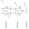
- Fig. 5 illustrates one embodiment of a current sensing circuit according to the present invention.
- the circuit comprises three parts, namely a differential current input stage 10, a differential voltage output stage 20 and a buffer stage 30 shown in Figs 5(a), (b) and (c) respectively.
- Fig. 5(a) shows the differential current input stage 10. This stage compares a sensor current I IN from a sensing device 14, such as a transducer, with a reference current I REF from a current source 16. V OUT1 and V OUT2 are the output voltages.
- the differential current input stage 10 comprises a first pair of matched transistors T1, T2 forming a current mirror, preferably a PMOS current mirror, as shown in Fig. 5(a).
- Each of these current mirror transistors T1, T2 is connected to a first common rail VDD.
- the gates of the current mirror pair of transistors are connected to each other, and the drain (preferably) of one of the current mirror transistors T2 is connected to the gate of that transistor T2.
- the differential current input stage 10 also comprises a matched, bias pair of transistors T4, T5.
- the bias transistors T4, T5 are NMOS transistors.
- Each of the bias transistors T4, T5 is connected in series to a respective one of the first current mirror transistors T1, T2.
- the gates of the bias transistors T4, T5 are biased to saturation by bias voltage V B1 .
- a node is provided between each first current mirror transistor and the respective bias transistor to form a first pair of nodes N1, N2.
- a first switch SW1 is connected between the first pair of nodes N1, N2.
- a current source 16 providing the reference current I REF is connected in series between a second common rail V SS and a respective one of the bias pair of transistors T5.
- the sensing device 14 providing the sensor current I IN is connected in series between the second common rail V SS and the other of the bias pair of transistors T4.
- a selecting means may be used to connect any one of a plurality of sensing devices between the second common rail VSS and the bias transistor T4 by means of a bit line 12.
- the differential current input stage has two output voltages V OUT1 and V OUT2 .
- the first output V OUT1 corresponds to the value of the reference current I REF and is taken from the second node N2.
- the second output V OUT2 corresponds to the value of the sensor current I IN and is taken from the first node N 1.
- the matching and biasing of input transistors T4 and T5 causes them to operate in saturation in order to minimise the effect of the input voltages of the current source 16 and the sensing device 14, which itself acts as a current source.
- the bias transistors T4, T5 act as spacers between respective current sources 14, 16 and current mirror transistors T1, T2.
- Fig. 5(b) shows the differential voltage output stage 20.
- the differential voltage output stage 20 comprises a pair of transistors T8, T9, which forms a second current mirror.
- Each of the second current mirror transistors T8, T9 is connected to a first common rail VDD.
- the current mirror is preferably a PMOS current mirror, as shown in Fig. 5(b).
- the gates of the second current mirror transistors are connected to each other, and the drain (preferably) of one of the second current mirror transistors T9 is connected to its gate.
- the differential voltage output stage 20 comprises a matched, differential or input pair of transistors T11, T12 each connected in series to a respective one of the current mirror transistors T8, T9.
- the input transistors are NMOS transistors.
- the gates of the input transistors T11, T12 are connected to output voltages V OUT1 and V OUT2 of the differential current input stage 10.
- the differential voltage output stage 20 further comprises a current source transistor T13, connected in series between the second common rail V SS and a node CN, which is itself connected to both the input transistors T11, T12.
- the gate of the current source transistor T13 is biased by bias voltage V B2 to saturation so that a uniform, constant current is provided to both the matched input transistors T11, T12.
- transistor T13 is biased in saturation and is used as a differential tail current source.
- the current that the input transistors T11, T12 pass is determined by the input voltages V OUT1 and V OUT2 .
- the differential current output stage 20 is similar to the prior art differential shown in Fig. 3. However, node is provided between each first current mirror transistor T8, T9 and the respective bias transistor T11, T12 to form a second pair of nodes N3, N4.
- a second switch SW2 is connected between the second pair of nodes N3, N4.
- the second switch SW2 is connected between the drain terminals of NMOS current mirror transistors T8 and T9 and is controlled by the signal PRE.
- the output voltage V OUT of the differential voltage output stage 20 is the voltage at the node N3 between the current mirror transistor T8 and the input transistor T11.
- switch SW2 is closed. Once switch SW2 is opened, the output voltage V OUT is an amplified version of (V OUT1 - V OUT2 ) up to its dynamic range and is wide enough to be distinguished by the buffer stage as shown in Fig. 5(c). However, the dynamic range is not the rail-to-rail range (V DD - V SS ).
- switches SW1 and SW2 provide an equalising function so that the set-up time of the sensing circuit is reduced.
- Fig. 5(c) shows a buffer stage consisting of two inverters U1 and U2. The input is connected to the output voltage V OUT of the differential current output stage in Fig. 5(b).
- the function of the buffer stage 30 is to provide a clean digital signal V SENOUT corresponding to the analogue output signal V OUT from the differential voltage output stage 20.
- the buffer stage provides rail-to-rail output voltage V SENOUT of the sensing circuit and provides sufficient drive current to the subsequent stages.
- Figs. 6(a) and (b) show the implementation of the circuits illustrated in Figs. 5(a) and (b) using PMOS transistors T3, T10 as the equalisation switches SW1 and SW2.
- Fig. 6 (c) is the same as Fig. 5(c) and will not be described further.
- the present invention provides a sensing circuit integrating one or more sensing devices and a reference current source. More specifically, the sensing device or devices and a reference current source form part of the integrated sensing circuit and can be formed on a monolithic chip. In addition, the reference current source acts as a dummy sensing device.
- the current sensing circuit of the present invention is a differential current detection circuit, which compares the output of an active sensing device with the output of a dummy sensing device. Since they are formed in an integrated circuit, both the active and dummy sensing devices operate under the same conditions except for the parameters related to the specific event the sensing circuit is designed to sense. To achieve this, the present invention uses an input stage, in particular a differential current input stage 10, to sense and amplify the current difference between the active sensing device and the dummy sensing device and to interface with the subsequent differential voltage comparator.
- the active sensing device and the dummy sensing device may be formed during the same process steps and are subject to the same operating conditions, such as temperature and ageing. In addition, they will have the same tolerances in transistor characteristics since they will be manufactured using the same fabrication process technology and/or the same variations in process conditions.
- the dummy sensing device 16 should have the transistor characteristics of an average active sensing device 14.
- dummy switching could be provided between the dummy sensing device 16 and the remainder of the sensing circuit to mirror the switching for the active sensing devices 14 into and out of the sensing circuit.
- the threshold detection level I REF may also be adjustable. Preferably, the selection of a suitable threshold detection level should be performed automatically by the sensing circuit.
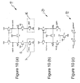
- Fig. 7(a) shows how, in one embodiment, the sensor input current I IN can be supplied by the output transistor T6 of a sensing device 14 acting as a current source.
- the reference current I REF can be supplied by the output transistor T7 of a dummy sensing device 16 acting as a reference current source.
- V SEN indicates the nodal voltage of the active sensing device 14, which supplies the sensor current I IN .
- V REF indicates the nodal voltage of the dummy sensing device 16 of the same structure, which supplies the reference current I REF .
- the dummy sensing device 16 comprises an equivalent transistor T7, which is manufactured and used under the same conditions as the transistor T6 of the active sensing device 14.
- the link 12 between the sensing device may be a bit line, which can be implemented as a physically long line shared by many other similarly structured sensing devices.
- Figs. 7(b) and (c) are the same as Figs. 6(b) and (c) and will not be described further.
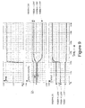
- Fig. 8 shows the DC transfer characteristics of the sensing circuit shown in Fig. 7. Specifically, Fig. 8 shows the DC transfer characteristics of V OUT from the differential voltage output stage 20 and V SENOUT from the buffer stage 30, for a range reference voltages V REF , as the nodal voltage V SEN increases.
- the input threshold of the first inverter U1 in the buffer stage 30 is set between the lower horizontal line for V OUT on the left hand side of the figure (when no event is sensed) and the upper horizontal line for V OUT on the right hand side of the figure (when an event is sensed).
- the input threshold is set between approximately 1.0V and 2.0V in this embodiment.
- the precharge control signal PRE is held low and the PMOS transistors T3, T10 are switched on. Subsequently, the precharge control signal PRE is forced high and the PMOS transistors T3, T10 are switched off.
- the switches SW1 and SW2 may be implemented using small NMOS transistors, which have higher mobility and lower on-resistance.
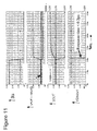
- Fig. 10 shows simulation results for the sensing circuit illustrated in Fig. 10. Since the switches SW1, SW2 are implemented using NMOS transistors instead of PMOS transistors, the polarity of the precharge control signal PRE is reversed compared with Fig. 9. The simulation results illustrated in Fig. 11 show a good improvement. In particular, the values of (V OUT1 - V OUT2 ) from the differential current input stage 10 and of V OUT from the differential voltage output stage 20 are substantially the same when the switches SW1, SW2 are closed, regardless of the difference between V SEN and V REF .
- the threshold voltage of the first inverter U1 of the buffer stage 30 can be easily set so that events can be reliably and accurately detected, but only after the precharge phase when the switches SW1, SW2 have been opened.
- the response time of the sensing circuit at V SENOUT is less than 0.2 ⁇ s for circuits implemented using polysilicon TFTs.
- sensing circuit applications of the above-described sensing circuit are wide. They include, but are not limited to, fingerprint sensors, memory sense amplifiers and biosensors. These applications are described briefly described below.
- Fig. 12 illustrates one embodiment of a fingerprint sensor.
- the sensing device 14 corresponds with the sensing device 14 shown in Fig. 10(a). It comprises a reference capacitance of a fixed value C REF ; the capacitance between a portion of a finger and a sensing pixel plate C FIN ; an applied excitation voltage V IN ; and an output transistor T6.
- the output transistor T6 of the sensing device 14 corresponds with the output transistor T6 of the sensing device 14 shown in Fig. 10(a).
- V BODY is the DC potential of a human body and I OUT is the output current of the sensing device 14. Accordingly, the output current I OUT of the sensing device 14 in Fig.
- the sensor 18 of the fingerprint sensor in Fig. 12 corresponds with the portions of the sensing circuit in Figs. 10(a), (b) and (c) other than the sensing device 14.
- a dummy sensing device 16 of the sensor 18 is formed to have the same structure as the sensing device 14. A voltage is forced at the gate terminal of the equivalent transistor T7 of the dummy sensing device 16.
- a large array of small sensing devices 14, each having a sensing pixel plate, is provided in a matrix.
- a finger is placed over the array of sensing plates and the sensing devices are sequentially switched into the sensing circuit. Equivalent dummy switching may be provided for the dummy sensing device 16. If a valley on the surface of the finger is placed over a particular sensing plate, then the capacitance between them will be comparatively low and no event is detected for that plate. In contrast, if a ridge on the surface of the finger is placed over a particular sensing plate, then the capacitance between them will be comparatively high and an event is detected for that plate. In this way, a map of ridges and valleys on the finger - in other words, an image of a fingerprint - can be determined.
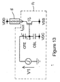
- Fig. 13 shows a sensing circuit used for a memory application.
- C FE in the sensing device 14 is a ferroelectric capacitor under interrogation.
- Capacitor C BL is the bit line capacitance and is biased to V DC .
- Capacitors C FE and C BL are connected in series.
- the resultant nodal voltage at node N due to the excitation voltage V 1 is fed to the gate of transistor T6, which translates it into a current for sensing by the current sensing circuit.
- the output transistor T6 of the sensing device 14 shown in Fig. 13 corresponds with the output transistor T6 of the sensing device 14 shown in Fig. 10(a).
- Output current I OUT is the output current of the sensing device 14.
- the output current I OUT of the sensing device 14 in Fig. 13 corresponds with the input current I IN provided by the sensing device 14 in the differential current input stage 10 of Fig. 6(a).
- the sensor 18 of the memory application in Fig. 13 corresponds with the portions of the sensing circuit in Figs. 10(a), (b) and (c) other than the sensing device 14.
- a dummy sensing device 16 of the sensor 18 is formed to have the same structure as the sensing device 14.
- the dummy sensing device 16 is formed by providing a capacitor C FE with a known polarisation.
- the differential current input stage can function as the sense amplifier.
- a large array of sensing devices 14 is provided in a matrix and equivalent switching is provided for the dummy sensing device 16. This allows large space savings to be made and improves accuracy.
- Figure 14 shows a sensing circuit used for a biosensor application.
- V REF provides a potential by means of a terminal RE and through an electrolyte to a reference electrode.
- the reference electrode is an ion sensitive membrane and forms the gate of a field effect transistor (ISFET).
- ISFET field effect transistor
- the ISFET outputs a current level I OUT to the sensor 18.
- the ISFET of the sensing device 14 corresponds with the output transistor T6 of the sensing device 14 shown in Fig. 10(a). Accordingly, the output current I OUT of the sensing device 14 in Fig.
- the sensor 18 of the biosensor application in Fig. 14 corresponds with the portions of the sensing circuit in Figs. 10(a), (b) and (c) other than the sensing device 14.
- a sensing device 16 of the sensor 18 is formed to have the same structure as the sensing device 14.
- the dummy sensing device 16 is formed by coating an ISFET with a reference membrane.
- ISFET indium-semiconductor
- a large array of sensing devices 14 is commonly provided in a matrix. This allows large space savings to be made and improves accuracy.
- Different electrolytes may be provided for different sensing devices. Alternatively, the same electrolyte may be provided for two, more than two or all the sensing devices, as a check.
- the term sensing device has been used to describe a single device, such as a transducer, a property of which changes in response to a specific event.
- the sensing device outputs a current.
- each such a sensing device is commonly called a sensing cell and the active matrix of sensing cells is commonly called a sensing device.
- a sensing device comprising a plurality of sensing cells can be connected into the sensing circuit of the present invention.
- the present invention provides a current sensing circuit, which compares a sensed current with a reference current.
- the reference current is generated under the same conditions as the sensed current and the detection of an event is therefore more accurately performed. Consequently, prior art difficulties in accurately selecting and setting a fixed reference voltage are overcome.
- the respective sources of the sensed current and the reference current are formed in the same IC, they are subject to the same process variations in fabrication and undergo the same degradation due to ageing and adverse environmental factors, such as temperature, humidity and pH.
- switches SW1 and SW2 it is not necessary to provide two switches SW1 and SW2. Moreover, if two switches are provided, they need not be controlled by the same signal, although this is preferable. In addition, it is not necessary that the differential current input and differential voltage output stages be implemented using the specific circuitry described. For example, they need not be implemented using polysilicon TFTs.
Abstract
Description
- The present invention relates to sensing devices and sensing circuits, which may include such sensing devices. The present invention especially relates to current sensing circuits.
- The resistance of many sensor devices changes in response to a specific event. Such resistance changes can be converted by a sensing circuit to changes in voltage or changes in current, which can then be measured to determine whether the event has occurred and, potentially, the scale of the event.
- Thus, Fig. 1 shows a prior
art sensing circuit 100 including a knownsensing device 2. Thesensing device 2 may be provided as an integrated circuit (IC), which can be connected into thesensing circuit 100. Thesensing circuit 100 includes a constant current source IIN connected between earth and the positive input of avoltage comparator 1. One terminal of thesensing device 2 is connected between the current source IIN and the respective, positive input of the voltage comparator. The other terminal of thesensing device 2 is earthed. The negative input of thevoltage comparator 1 is connected to a reference voltage source VREF. - Before the occurrence of an event, the
sensing device 2 has a predetermined resistance and, consequently, the voltage applied to the positive input of the voltage comparator is consistently above (or below) VREF. A corresponding signal VOUT (ON or OFF) is output by thevoltage comparator 1. After the occurrence of an event, the resistance of thesensing device 2 is changed. This lowers (or raises) the voltage applied to the positive terminal of thevoltage comparator 1 below (or above) VREF. The signal that is output by thevoltage comparator 1 is therefore switched to indicate the occurrence of the event. In other words, thevoltage comparator 1 implements a discrimination function based on comparison of a voltage changed by thesensing device 2 and a reference voltage VREF. - Fig. 2 also shows a prior
art sensing circuit 200 including a knownsensing device 2. However, in this case the positive input of thevoltage comparator 1 is connected to the reference voltage VREF. The negative input of thevoltage comparator 1 is connected to the output of anoperational amplifier 3, which has a negative feedback resistor R. The positive input of theoperational amplifier 3 is earthed. A bias voltage source VBIAS is connected to the negative terminal of theoperational amplifier 3, with thesensing device 2 connected in series between the bias voltage source VBIAS and the negative terminal. - Before the occurrence of an event, the
sensing device 2 has a predetermined resistance and a corresponding current is supplied to the negative input of theoperational amplifier 3. Theoperational amplifier 3 provides current to voltage conversion gain and a corresponding voltage is therefore applied to the negative terminal of the comparator. This corresponding voltage is consistently above (or below) the reference voltage VREF and a corresponding signal VOUT (OFF or ON) is output by thevoltage comparator 1. After the occurrence of an event, the resistance of thesensing device 2 is changed. This lowers (or raises) the current supplied to the negative terminal of theoperational amplifier 3. Hence, the voltage applied to the negative terminal of thevoltage comparator 1 is lowered below (or raised above) VREF. The signal VOUT output by thevoltage comparator 1 is therefore switched to indicate the occurrence of the event. Again, thevoltage comparator 1 implements a discrimination function. However, this discrimination is performed by converting the current of thesensor device 2 to a voltage and then comparing that voltage with a reference voltage VREF. - It is often necessary to amplify the signal further for subsequent stages of electronics.
- In the circuits of both Figs. 1 and 2, the change in the resistance of the
sensing device 2 is converted and compared with a constant threshold voltage signal VREF to discriminate the occurrence of an event. However, in practice the output of the sensing device is dependent not only on a specific parameter related to the event but also on other factors such as temperature and ageing. In addition, a tolerance exists in the characteristics of the sensing devices due to the fabrication process technology and/or variations in process conditions. - As shown in Figs. 1 and 2, a
differential voltage comparator 1 is commonly used to implement the discrimination function. A typical differential circuit for implementing thedifferential voltage comparator 1 is shown in Fig. 3. Specifically, the differential circuit comprises a current mirror pair of transistors T101, T102, each connected to a first common rail VDD. The gates of the current mirror pair of transistors are connected to each other, and the drain of one of the second current mirror transistors T101 is connected to its gate. - In addition, the differential circuit comprises an input or differential pair of transistors T103, T104, each connected in series to a respective one of the current mirror transistors. The gates of the input pair of transistors are connected to input voltages VIN1 and VIN2. Specifically, when used in the sensing circuit of Fig. 1, the gate of input transistor T104 would be connected to current source IIN and the gate of input transistor T103 would be connected to reference voltage VREF. The voltages applied to the gates of the input transistors T103, T104 determine the current passed by the input transistors T103, T104.
- The differential circuit further comprises a current source transistor T105, connected in series between a second common rail Vss and a node, which is itself connected to both the input transistors T103, T104. The gate of the current source transistor T105 is biased to saturation so that a uniform, constant current is provided to both the matched input transistors T103, T104. However, the current that the input transistors pass is determined by the input voltages VIN1 and VIN2.
- The output voltage VOUT of the differential circuit is the voltage at a node between the current mirror transistor T102 and the input transistor T104.
- As shown in Fig. 4, an output amplification stage may be added to the differential circuit shown in Fig. 3. The output amplification stage comprises transistors T106, T107 connected between the common rails VDD and VSS, in series with each other and in parallel to the other transistors T101-T104. The voltage at the node between the current mirror transistor T102 and the input transistor T104 of the differential circuit is the input voltage to the gate of transistor T106 and the gate of transistor T107 is separately controlled. In this case, it becomes an operational amplifier as shown in Figure 4.
- As noted above, prior art sensing circuits compare the output of a sensing device with a predetermined reference voltage VREF. However, as discussed above, in practice the output of a sensing device is dependent not only on a specific parameter related to the event to be sensed but also on other factors such as temperature and ageing. In addition, a tolerance exists in the characteristics of the sensing devices due to the fabrication process technology and/or variations in process conditions. Consequently, the output of the sensing device does not always cross the threshold provided by the predetermined reference voltage VREF and events are not reliably sensed.
- These difficulties are exacerbated when several sensing devices are provided, which can be sequentially connected into the sensing circuit. As the sensing devices age, their outputs will vary from each other so that some sensing devices will correctly sense an event and others will not.
- According to a first aspect of the present invention, there is provided a current sensing circuit comprising a differential current input stage connected to a differential voltage output stage.
- The differential current input stage may comprise a reference current input from a current source and a sensor current input from a sensing device. It may further comprise a first voltage output corresponding to the reference current and a second voltage output corresponding to the sensor current; and still further a first switch for substantially equalising the first and second voltage outputs when closed.
- The first and second voltage outputs from the differential current input stage may be respective inputs to the differential voltage output stage, which then outputs a differential output voltage corresponding to the difference between the first and second voltage outputs.
- The differential voltage output stage may comprise a second switch for substantially eliminating the differential output voltage when closed.
- The differential current input stage may comprise:
- a first pair of current mirror transistors, each connected to a first common rail, the gates of the first pair of current mirror transistors being connected to each other, and a source or drain of one of the first pair of current mirror transistors being connected to its gate;
- a pair of bias transistors, each connected in series to a respective one of the first pair of current mirror transistors, the gates of the pair of bias transistors being biased to saturation;
- a first pair of nodes, each disposed between one of the pair of first current mirror transistors and a respective one of the pair of bias transistors; and
- a first switch connected between the first pair of nodes; wherein the current source is connected in series between a second common rail and a respective one of the pair of bias transistors; and
-
- The differential voltage output stage may comprise:
- a second pair of current mirror transistors, each connected to the first common rail, the gates of the second pair of current mirror transistors being connected to each other, and a source or drain of one of the second pair of current mirror transistors being connected to its gate;
- a pair of input transistors, each connected in series to a respective one of the second pair of current mirror transistors, the gates of the pair of input transistors being connected to respective ones of the first pair of nodes;
- a second pair of nodes, each disposed between one of the second pair of current mirror transistors and a respective one of the pair of input transistors;
- a second switch connected between the second pair of nodes; and
- a current source transistor, connected in series between the second common rail and a further node, the further node being connected to both the input transistors, and the gate of the current source transistor being biased to saturation; wherein the voltage of the node of the second pair of nodes that is connected to the other of the second pair of current mirror transistors is a differential output voltage.
-
- The differential current input stage may comprise a first pair of current mirror transistors, a first switch between the sources or drains of the first pair of current mirror transistors, and a pair of bias transistors; and
the differential voltage output stage may comprise a second pair of current mirror transistors, a second switch between the sources or drains of the second pair of current mirror transistors, a pair of bias transistors the gates of which are connected to the outputs of the differential current input stage, and a differential tail current source. - In any case, the first pair of current mirror transistors may be matched, the pair of bias transistors may be matched, the second pair of current mirror transistors may be matched and the pair of input transistors may be matched.
- In one embodiment, the switch or switches are arranged to be closed before sensing and to be open during sensing. The switch or switches may be N-type switches. In addition, the switch or switches and all the transistors may be polysilicon thin film transistors. Where provided, the first and second switches may be controlled using the same signal.
- The current sensing circuit described above may comprise: a plurality of sensing devices; and selecting means for selecting which sensing device provides the sensor current input. The plurality of sensing devices may form an active matrix. In addition, where provided, the switch or switches may be arranged to be closed while the sensor current input is selected and to be open after the sensor current input is selected. Preferably, the current source and the sensing device are operated under the same conditions.
- The current source may be adjustable. Also, the sensing device may comprise one or more capacitors.
- The current sensing circuit described above may also comprise a further stage connected to the output of the differential voltage output stage for providing a digital output signal. The current sensing circuit may be formed as a single integrated circuit.
- According to another aspect of the present invention, there is provided a fingerprint sensor comprising a current sensing circuit as described above.
- According to another aspect of the present invention, there is provided an electronic memory comprising a current sensing circuit as described above.
- According to another aspect of the present invention, there is provided a biosensor comprising a current sensing circuit as described above.
- According to yet another aspect of the present invention, there is provided a method of sensing an event, the method comprising using a sensing device as described above..
- According to another aspect of the present invention, there is provided a method of sensing an event comprising:
- sensing a dummy sensor current;
- sensing an active sensor current that changes in response to an event; and
- comparing the dummy sensor current and the active sensor current to determine whether an event has occurred.
-
- In this method, the step of comparing may comprise:
- converting the dummy sensor current and the active sensor current into a first voltage and a second voltage respectively; and
- obtaining a further voltage corresponding to the difference between the first voltage and the second voltage, said further voltage being indicative of the occurrence of an event.
-
- The method may further comprise the step of converting said further voltage into a digital signal.
- Embodiments of the present invention will now be described by way of further example only and with reference to the accompanying drawings, in which:
- Fig. 1 illustrates a prior art sensing circuit;
- Fig. 2 illustrates another prior art sensing circuit;
- Fig. 3 illustrates a prior art differential circuit;
- Fig. 4 illustrates a prior art operational amplifier;
- Fig. 5 is a schematic representation of a sensing circuit according to the present invention;
- Fig. 6 is a schematic representation of another sensing circuit according to the present invention;
- Fig. 7 is a schematic representation of another sensing circuit according to the present invention;
- Fig. 8 illustrates the results of a DC simulation of the sensing circuit shown in Fig. 7 and shows various inputs and outputs of that sensing circuit;
- Fig. 9 also illustrates the results of a transient simulation of the sensing circuit shown in Fig. 7 and shows other inputs and outputs of that sensing circuit;
- Fig. 10 is a schematic representation of another sensing circuit according to the present invention;
- Fig. 11 illustrates the results of a transient simulation of the sensing circuit shown in Fig. 10 and shows various inputs and outputs of that sensing circuit;
- Fig. 12 shows a fingerprint sensor using a sensing circuit of the present invention;
- Fig. 13 shows a memory device using a sensing circuit of the present invention; and
- Fig. 14 shows a biosensor using a sensing circuit of the present invention.
-
- In the present invention, all sensing circuits and sensing devices may be fabricated using thin film transistors formed using polycrystalline semiconductor material (for example, polysilicon TFTs) on the same insulating substrate. However, this invention can also be implemented using other technologies, in particular CMOS technologies. Moreover, a reference to a gate, source or drain of a transistor is intended throughout this application as a reference to a base, emitter and collector of a transistor, as appropriate, when the present invention is implemented using transistors to which these terms generally apply.
- Fig. 5 illustrates one embodiment of a current sensing circuit according to the present invention. The circuit comprises three parts, namely a differential
current input stage 10, a differentialvoltage output stage 20 and a buffer stage 30 shown in Figs 5(a), (b) and (c) respectively. - Fig. 5(a) shows the differential
current input stage 10. This stage compares a sensor current IIN from asensing device 14, such as a transducer, with a reference current IREF from acurrent source 16. VOUT1 and VOUT2 are the output voltages. - More specifically, the differential
current input stage 10 comprises a first pair of matched transistors T1, T2 forming a current mirror, preferably a PMOS current mirror, as shown in Fig. 5(a). Each of these current mirror transistors T1, T2 is connected to a first common rail VDD. The gates of the current mirror pair of transistors are connected to each other, and the drain (preferably) of one of the current mirror transistors T2 is connected to the gate of that transistor T2. - The differential
current input stage 10 also comprises a matched, bias pair of transistors T4, T5. Preferably, the bias transistors T4, T5 are NMOS transistors. Each of the bias transistors T4, T5 is connected in series to a respective one of the first current mirror transistors T1, T2. The gates of the bias transistors T4, T5 are biased to saturation by bias voltage VB1. A node is provided between each first current mirror transistor and the respective bias transistor to form a first pair of nodes N1, N2. A first switch SW1 is connected between the first pair of nodes N1, N2. - A
current source 16 providing the reference current IREF is connected in series between a second common rail VSS and a respective one of the bias pair of transistors T5. Thesensing device 14 providing the sensor current IIN is connected in series between the second common rail VSS and the other of the bias pair of transistors T4. However, in other embodiments a selecting means may be used to connect any one of a plurality of sensing devices between the second common rail VSS and the bias transistor T4 by means of abit line 12. - The differential current input stage has two output voltages VOUT1 and VOUT2. The first output VOUT1 corresponds to the value of the reference current IREF and is taken from the second node N2. The second output VOUT2 corresponds to the value of the sensor current IIN and is taken from the
first node N 1. - The matching and biasing of input transistors T4 and T5 causes them to operate in saturation in order to minimise the effect of the input voltages of the
current source 16 and thesensing device 14, which itself acts as a current source. Effectively, the bias transistors T4, T5 act as spacers between respectivecurrent sources - The switch SW1, which is connected between the two output voltages VOUT1 and VOUT2, is controlled by a signal PRE. Before a sensing operation is carried out, switch SW1 is closed to equalise the output voltages, so VOUT1 = VOUT2. At this moment, connection to the sensing device or transducer can be reconfigured, without affecting the output. Thus, where a plurality of sensing devices is provided, they can be individually selected to provide the sensor current input IIN, without affecting the output of the current sensing circuit. Once SW1 is opened any current difference (IIN - IREF) is converted to a voltage difference (VOUT1 - VOUT2). If there is no current difference (i.e. IIN = IREF), VOUT1 = VOUT2 since T1 and T2 are matched.
- Fig. 5(b) shows the differential
voltage output stage 20. The differentialvoltage output stage 20 comprises a pair of transistors T8, T9, which forms a second current mirror. Each of the second current mirror transistors T8, T9 is connected to a first common rail VDD. The current mirror is preferably a PMOS current mirror, as shown in Fig. 5(b). The gates of the second current mirror transistors are connected to each other, and the drain (preferably) of one of the second current mirror transistors T9 is connected to its gate. - In addition, the differential
voltage output stage 20 comprises a matched, differential or input pair of transistors T11, T12 each connected in series to a respective one of the current mirror transistors T8, T9. Preferably, the input transistors are NMOS transistors. The gates of the input transistors T11, T12 are connected to output voltages VOUT1 and VOUT2 of the differentialcurrent input stage 10. - The differential
voltage output stage 20 further comprises a current source transistor T13, connected in series between the second common rail VSS and a node CN, which is itself connected to both the input transistors T11, T12. The gate of the current source transistor T13 is biased by bias voltage VB2 to saturation so that a uniform, constant current is provided to both the matched input transistors T11, T12. Thus, transistor T13 is biased in saturation and is used as a differential tail current source. However, the current that the input transistors T11, T12 pass is determined by the input voltages VOUT1 and VOUT2. - Thus, the differential
current output stage 20 is similar to the prior art differential shown in Fig. 3. However, node is provided between each first current mirror transistor T8, T9 and the respective bias transistor T11, T12 to form a second pair of nodes N3, N4. A second switch SW2 is connected between the second pair of nodes N3, N4. Preferably, the second switch SW2 is connected between the drain terminals of NMOS current mirror transistors T8 and T9 and is controlled by the signal PRE. - The output voltage VOUT of the differential
voltage output stage 20 is the voltage at the node N3 between the current mirror transistor T8 and the input transistor T11. - Initially, switch SW2 is closed. Once switch SW2 is opened, the output voltage VOUT is an amplified version of (VOUT1 - VOUT2) up to its dynamic range and is wide enough to be distinguished by the buffer stage as shown in Fig. 5(c). However, the dynamic range is not the rail-to-rail range (VDD - VSS).
- Effectively, switches SW1 and SW2 provide an equalising function so that the set-up time of the sensing circuit is reduced.
- Fig. 5(c) shows a buffer stage consisting of two inverters U1 and U2. The input is connected to the output voltage VOUT of the differential current output stage in Fig. 5(b). The function of the buffer stage 30 is to provide a clean digital signal VSENOUT corresponding to the analogue output signal VOUT from the differential
voltage output stage 20. In particular, the buffer stage provides rail-to-rail output voltage VSENOUT of the sensing circuit and provides sufficient drive current to the subsequent stages. - Figs. 6(a) and (b) show the implementation of the circuits illustrated in Figs. 5(a) and (b) using PMOS transistors T3, T10 as the equalisation switches SW1 and SW2. Fig. 6 (c) is the same as Fig. 5(c) and will not be described further.
- Accordingly, using semiconductor process technologies, the present invention provides a sensing circuit integrating one or more sensing devices and a reference current source. More specifically, the sensing device or devices and a reference current source form part of the integrated sensing circuit and can be formed on a monolithic chip. In addition, the reference current source acts as a dummy sensing device. Thus, the current sensing circuit of the present invention is a differential current detection circuit, which compares the output of an active sensing device with the output of a dummy sensing device. Since they are formed in an integrated circuit, both the active and dummy sensing devices operate under the same conditions except for the parameters related to the specific event the sensing circuit is designed to sense. To achieve this, the present invention uses an input stage, in particular a differential
current input stage 10, to sense and amplify the current difference between the active sensing device and the dummy sensing device and to interface with the subsequent differential voltage comparator. - The active sensing device and the dummy sensing device may be formed during the same process steps and are subject to the same operating conditions, such as temperature and ageing. In addition, they will have the same tolerances in transistor characteristics since they will be manufactured using the same fabrication process technology and/or the same variations in process conditions.
- Effectively then, where a matrix of individually selectable active sensing devices is provided, the
dummy sensing device 16 should have the transistor characteristics of an averageactive sensing device 14. To further improve the effectiveness of the sensing circuit, dummy switching could be provided between thedummy sensing device 16 and the remainder of the sensing circuit to mirror the switching for theactive sensing devices 14 into and out of the sensing circuit. In addition, the threshold detection level IREF may also be adjustable. Preferably, the selection of a suitable threshold detection level should be performed automatically by the sensing circuit. - Fig. 7(a) shows how, in one embodiment, the sensor input current IIN can be supplied by the output transistor T6 of a
sensing device 14 acting as a current source. Similarly, the reference current IREF can be supplied by the output transistor T7 of adummy sensing device 16 acting as a reference current source. VSEN indicates the nodal voltage of theactive sensing device 14, which supplies the sensor current IIN. VREF indicates the nodal voltage of thedummy sensing device 16 of the same structure, which supplies the reference current IREF. Thus, thedummy sensing device 16 comprises an equivalent transistor T7, which is manufactured and used under the same conditions as the transistor T6 of theactive sensing device 14. Thelink 12 between the sensing device may be a bit line, which can be implemented as a physically long line shared by many other similarly structured sensing devices. Theseactive sensing devices 14 can be made inactive by setting VSEN=0V. Similarly, thedummy sensing device 16 can be made inactive by setting VREF=0V. Figs. 7(b) and (c) are the same as Figs. 6(b) and (c) and will not be described further. - Fig. 8 shows the DC transfer characteristics of the sensing circuit shown in Fig. 7. Specifically, Fig. 8 shows the DC transfer characteristics of VOUT from the differential
voltage output stage 20 and VSENOUT from the buffer stage 30, for a range reference voltages VREF, as the nodal voltage VSEN increases. As will be clear from the figure, the input threshold of the first inverter U1 in the buffer stage 30 is set between the lower horizontal line for VOUT on the left hand side of the figure (when no event is sensed) and the upper horizontal line for VOUT on the right hand side of the figure (when an event is sensed). Thus, the input threshold is set between approximately 1.0V and 2.0V in this embodiment. - However, there is a disadvantage in using PMOS transistors T3, T10 for the precharge switches SW1 and SW2. Fig. 9 shows simulation results for the sensing circuit shown in Fig. 7 where VREF is set so VREF=1.2V and VSEN is set so VSEN=1.15V, 1.20V and 1.25V respectively. Specifically, Fig. 9 shows how, for these parameters, the difference (VOUT1 - VOUT2) between the outputs of the differential
current input stage 10 and the output VOUT of the differentialvoltage output stage 20 vary as the precharge control signal PRE for the equalising transistors T3, T10 is varied. - In the initial period, the precharge control signal PRE is held low and the PMOS transistors T3, T10 are switched on. Subsequently, the precharge control signal PRE is forced high and the PMOS transistors T3, T10 are switched off.
- The results demonstrate that when VREF=VSEN and SW1 and SW2 are closed in the initial period (time=0 - 2 s), the output voltage difference (VOUT1 - VOUT1) = 0. During the period when the equalising switches SW1, SW2 are closed, the output voltages VOUT1 and VOUT2 should also be equal regardless of the difference between VSEN and VREF. However, the results of the simulation demonstrate that (VOUT1 - VOUT2) ≠ 0 when VREF ≠ VSEN. Moreover, the value of (VOUT1 - VOUT2) changes as the difference between VSEN and VREF changes. This is potentially problematic. In particular, the sensing circuit could erroneously detect an event during the precharge phase, when the switches T3, T10 are closed.
- In addition, the mobility of PMOS transistors is low and their resistance is correspondingly high. Thus, larger sized PMOS transistors are required for switches SW1, SW2 for the sensing circuit to operate effectively. However, a larger sized transistor contributes a larger feedthrough effect. This upsets the output voltage VOUT when the switches are turned off.
- To solve this problem, the switches SW1 and SW2 may be implemented using small NMOS transistors, which have higher mobility and lower on-resistance. This implementation is shown in Fig. 10. Fig. 11 shows simulation results for the sensing circuit illustrated in Fig. 10. Since the switches SW1, SW2 are implemented using NMOS transistors instead of PMOS transistors, the polarity of the precharge control signal PRE is reversed compared with Fig. 9. The simulation results illustrated in Fig. 11 show a good improvement. In particular, the values of (VOUT1 - VOUT2) from the differential
current input stage 10 and of VOUT from the differentialvoltage output stage 20 are substantially the same when the switches SW1, SW2 are closed, regardless of the difference between VSEN and VREF. Thus, the threshold voltage of the first inverter U1 of the buffer stage 30 can be easily set so that events can be reliably and accurately detected, but only after the precharge phase when the switches SW1, SW2 have been opened. Moreover, the response time of the sensing circuit at VSENOUT is less than 0.2µs for circuits implemented using polysilicon TFTs. Thus, each sensing device in a large active matrix array can be quickly and accurately switched into the sensing circuit for sensing. - Applications of the above-described sensing circuit are wide. They include, but are not limited to, fingerprint sensors, memory sense amplifiers and biosensors. These applications are described briefly described below.
- Fig. 12 illustrates one embodiment of a fingerprint sensor. Here, the
sensing device 14 corresponds with thesensing device 14 shown in Fig. 10(a). It comprises a reference capacitance of a fixed value CREF; the capacitance between a portion of a finger and a sensing pixel plate CFIN; an applied excitation voltage VIN; and an output transistor T6. The output transistor T6 of thesensing device 14 corresponds with the output transistor T6 of thesensing device 14 shown in Fig. 10(a). VBODY is the DC potential of a human body and IOUT is the output current of thesensing device 14. Accordingly, the output current IOUT of thesensing device 14 in Fig. 12 corresponds with input current IIN that is provided by thesensing device 14 in the differentialcurrent input stage 10 of Fig. 6(a). Thus, thesensor 18 of the fingerprint sensor in Fig. 12 corresponds with the portions of the sensing circuit in Figs. 10(a), (b) and (c) other than thesensing device 14. - A
dummy sensing device 16 of thesensor 18 is formed to have the same structure as thesensing device 14. A voltage is forced at the gate terminal of the equivalent transistor T7 of thedummy sensing device 16. - In practice, a large array of
small sensing devices 14, each having a sensing pixel plate, is provided in a matrix. A finger is placed over the array of sensing plates and the sensing devices are sequentially switched into the sensing circuit. Equivalent dummy switching may be provided for thedummy sensing device 16. If a valley on the surface of the finger is placed over a particular sensing plate, then the capacitance between them will be comparatively low and no event is detected for that plate. In contrast, if a ridge on the surface of the finger is placed over a particular sensing plate, then the capacitance between them will be comparatively high and an event is detected for that plate. In this way, a map of ridges and valleys on the finger - in other words, an image of a fingerprint - can be determined. - The use in the present invention of an active matrix of
sensing devices 14, which can be individually connected into the single sensing circuit, allows large space savings to be made. Consequently, the area within a sensing device for the reference capacitor CREF can be maximised, thereby further improving the accuracy of the device. - Fig. 13 shows a sensing circuit used for a memory application. Here, CFE in the
sensing device 14 is a ferroelectric capacitor under interrogation. Capacitor CBL is the bit line capacitance and is biased to VDC. Capacitors CFE and CBL are connected in series. The resultant nodal voltage at node N due to theexcitation voltage V 1 is fed to the gate of transistor T6, which translates it into a current for sensing by the current sensing circuit. Again, the output transistor T6 of thesensing device 14 shown in Fig. 13 corresponds with the output transistor T6 of thesensing device 14 shown in Fig. 10(a). Output current IOUT is the output current of thesensing device 14. Accordingly, the output current IOUT of thesensing device 14 in Fig. 13 corresponds with the input current IIN provided by thesensing device 14 in the differentialcurrent input stage 10 of Fig. 6(a). Thus, thesensor 18 of the memory application in Fig. 13 corresponds with the portions of the sensing circuit in Figs. 10(a), (b) and (c) other than thesensing device 14. - A
dummy sensing device 16 of thesensor 18 is formed to have the same structure as thesensing device 14. In particular, thedummy sensing device 16 is formed by providing a capacitor CFE with a known polarisation. The differential current input stage can function as the sense amplifier. Again, in practice a large array ofsensing devices 14 is provided in a matrix and equivalent switching is provided for thedummy sensing device 16. This allows large space savings to be made and improves accuracy. - Figure 14 shows a sensing circuit used for a biosensor application. In the
sensing device 14, VREF provides a potential by means of a terminal RE and through an electrolyte to a reference electrode. The reference electrode is an ion sensitive membrane and forms the gate of a field effect transistor (ISFET). Depending on the concentration of a specific ion in the electrolyte (e.g. pH), the ISFET outputs a current level IOUT to thesensor 18. Again, the ISFET of thesensing device 14 corresponds with the output transistor T6 of thesensing device 14 shown in Fig. 10(a). Accordingly, the output current IOUT of thesensing device 14 in Fig. 14 corresponds with the input current IIN provided by thesensing device 14 in the differentialcurrent input stage 10 of Fig. 6(a). Thus, thesensor 18 of the biosensor application in Fig. 14 corresponds with the portions of the sensing circuit in Figs. 10(a), (b) and (c) other than thesensing device 14. - A
sensing device 16 of thesensor 18 is formed to have the same structure as thesensing device 14. In particular, thedummy sensing device 16 is formed by coating an ISFET with a reference membrane. Again, in practice a large array ofsensing devices 14 is commonly provided in a matrix. This allows large space savings to be made and improves accuracy. Different electrolytes may be provided for different sensing devices. Alternatively, the same electrolyte may be provided for two, more than two or all the sensing devices, as a check. - In the aforegoing description, the term sensing device has been used to describe a single device, such as a transducer, a property of which changes in response to a specific event. In the described embodiments of the present invention, the sensing device outputs a current. In the art, each such a sensing device is commonly called a sensing cell and the active matrix of sensing cells is commonly called a sensing device. Thus, a sensing device comprising a plurality of sensing cells can be connected into the sensing circuit of the present invention.
- Accordingly, the present invention provides a current sensing circuit, which compares a sensed current with a reference current. The reference current is generated under the same conditions as the sensed current and the detection of an event is therefore more accurately performed. Consequently, prior art difficulties in accurately selecting and setting a fixed reference voltage are overcome. Moreover, since the respective sources of the sensed current and the reference current are formed in the same IC, they are subject to the same process variations in fabrication and undergo the same degradation due to ageing and adverse environmental factors, such as temperature, humidity and pH.
- The aforegoing description has been given by way of example only and it will be appreciated by a person skilled in the art that modifications can be made without departing from the scope of the present invention.
- For example, it is not necessary to provide two switches SW1 and SW2. Moreover, if two switches are provided, they need not be controlled by the same signal, although this is preferable. In addition, it is not necessary that the differential current input and differential voltage output stages be implemented using the specific circuitry described. For example, they need not be implemented using polysilicon TFTs.
the sensing device is connected in series between the second common rail and the other of the pair of bias transistors.
Claims (28)
- A current sensing circuit comprising a differential current input stage connected to a differential voltage output stage, wherein the differential current input stage comprises a reference current input from a current source and a sensor current input from a sensing device.
- A current sensing circuit according to claim 1, wherein the differential current input stage further comprises a first voltage output corresponding to the reference current and a second voltage output corresponding to the sensor current.
- A current sensing circuit according to claim 2, wherein the differential current input stage further comprises a first switch for substantially equalising the first and second voltage outputs when closed.
- A current sensing circuit according to claim 2 or claim 3, wherein the first and second voltage outputs from the differential current input stage are respective inputs to the differential voltage output stage, which outputs a differential output voltage corresponding to the difference between the first and second voltage outputs.
- A current sensing circuit according to claim 4, wherein the differential voltage output stage comprises a second switch for substantially eliminating the differential output voltage when closed.
- A current sensing circuit according to claim 1, wherein the differential current input stage comprises:wherein the current source is connected in series between a second common rail and a respective one of the pair of bias transistors; anda first pair of current mirror transistors, each connected to a first common rail, the gates of the first pair of current mirror transistors being connected to each other, and a source or drain of one of the first pair of current mirror transistors being connected to its gate;a pair of bias transistors, each connected in series to a respective one of the first pair of current mirror transistors, the gates of the pair of bias transistors being biased to saturation;a first pair of nodes, each disposed between one of the pair of first current mirror transistors and a respective one of the pair of bias transistors; anda first switch connected between the first pair of nodes;
the sensing device is connected in series between the second common rail and the other of the pair of bias transistors. - A current sensing circuit according to claim 6, wherein the differential voltage output stage comprises:wherein the voltage of the node of the second pair of nodes that is connected to the other of the second pair of current mirror transistors is a differential output voltage.a second pair of current mirror transistors, each connected to the first common rail, the gates of the second pair of current mirror transistors being connected to each other, and a source or drain of one of the second pair of current mirror transistors being connected to its gate;a pair of input transistors, each connected in series to a respective one of the second pair of current mirror transistors, the gates of the pair of input transistors being connected to respective ones of the first pair of nodes;a second pair of nodes, each disposed between one of the second pair of current mirror transistors and a respective one of the pair of input transistors;a second switch connected between the second pair of nodes; anda current source transistor, connected in series between the second common rail and a further node, the further node being connected to both the input transistors, and the gate of the current source transistor being biased to saturation;
- A current sensing circuit according to claim 1, wherein
the differential current input stage further comprises a first pair of current mirror transistors, a first switch between the sources or drains of the first pair of current mirror transistors, and a pair of bias transistors; and
the differential voltage output stage comprises a second pair of current mirror transistors, a second switch between the sources or drains of the second pair of current mirror transistors, a pair of bias transistors the gates of which are connected to the outputs of the differential current input stage, and a differential tail current source. - A current sensing circuit according to claim 7 or claim 8, wherein the first pair of current mirror transistors is matched, the pair of bias transistors is matched, the second pair of current mirror transistors is matched and the pair of input transistors is matched.
- A current sensing circuit according to any one of claims 3 to 9, wherein the switch or switches are arranged to be closed before sensing and to be open during sensing.
- A current sensing circuit according to any one of claims 3 to 10, wherein the switch or switches are N-type switches.
- A current sensing circuit according to any one of claims 3 to 11, wherein the switch or switches and all the transistors are polysilicon thin film transistors.
- A current sensing circuit according to any one of claims 5 to 12, comprising said first and second switches, wherein said first and second switches are controlled using the same signal.
- A current sensing circuit according to any one of the preceding claims, comprising:a plurality of sensing devices; andselecting means for selecting which sensing device provides the sensor current input.
- A current sensing circuit according to claim 14, wherein the plurality of sensing devices forms an active matrix.
- A current sensing circuit according to claim 14 or claim 15 when dependent on claim 3, wherein the switch or switches are arranged to be closed while the sensor current input is selected and to be open after the sensor current input is selected.
- A current sensing circuit according to any one of the preceding claims, wherein the current source and the sensing device are operated under the same conditions.
- A current sensing circuit according to any one of the preceding claims, wherein the current source is adjustable.
- A current sensing circuit according to any one of the preceding claims, wherein the sensing device comprises one or more capacitors.
- A current sensing circuit according to any one of the preceding claims, further comprising a further stage connected to the output of the differential voltage output stage for providing a digital output signal.
- A current sensing circuit according to any one of the preceding claims, formed as a single integrated circuit.
- A fingerprint sensor comprising a current sensing circuit according to any one of the preceding claims.
- An electronic memory comprising a current sensing circuit according to any one of claims 1 to 21.
- A biosensor comprising a current sensing circuit according to any one of claims 1 to 21.
- A method of sensing an event, the method comprising using a sensing device according to any one of the preceding claims.
- A method of sensing an event comprising:sensing a dummy sensor current;sensing an active sensor current that changes in response to an event; andcomparing the dummy sensor current and the active sensor current to determine whether an event has occurred.
- A method according to claim 26, wherein the step of comparing comprises:converting the dummy sensor current and the active sensor current into a first voltage and a second voltage respectively; andobtaining a further voltage corresponding to the difference between the first voltage and the second voltage, said further voltage being indicative of the occurrence of an event.
- A method according to claim 27, further comprising the step of converting said further voltage into a digital signal.
Applications Claiming Priority (2)
| Application Number | Priority Date | Filing Date | Title |
|---|---|---|---|
| GB0320642A GB2405701A (en) | 2003-09-03 | 2003-09-03 | Differential current sensing circuit |
| GB0320642 | 2003-09-03 |
Publications (3)
| Publication Number | Publication Date |
|---|---|
| EP1512982A2 true EP1512982A2 (en) | 2005-03-09 |
| EP1512982A3 EP1512982A3 (en) | 2005-10-19 |
| EP1512982B1 EP1512982B1 (en) | 2008-08-20 |
Family
ID=28686845
Family Applications (1)
| Application Number | Title | Priority Date | Filing Date |
|---|---|---|---|
| EP04255131A Expired - Fee Related EP1512982B1 (en) | 2003-09-03 | 2004-08-26 | Sensing devices and sensing circuits |
Country Status (6)
| Country | Link |
|---|---|
| US (1) | US6937052B2 (en) |
| EP (1) | EP1512982B1 (en) |
| JP (1) | JP2005077409A (en) |
| CN (1) | CN100567903C (en) |
| DE (1) | DE602004015901D1 (en) |
| GB (1) | GB2405701A (en) |
Cited By (3)
| Publication number | Priority date | Publication date | Assignee | Title |
|---|---|---|---|---|
| WO2010088443A1 (en) * | 2009-01-29 | 2010-08-05 | Qualcomm Incorporated | In-situ resistance measurement for magnetic random access memory (mram) |
| CN105988036A (en) * | 2015-03-19 | 2016-10-05 | 精工半导体有限公司 | Current detection circuit |
| EP3671199A1 (en) * | 2018-12-18 | 2020-06-24 | Ecole Polytechnique Federale de Lausanne (EPFL) | Negative capacitance semiconductor sensor |
Families Citing this family (36)
| Publication number | Priority date | Publication date | Assignee | Title |
|---|---|---|---|---|
| US7221605B2 (en) * | 2004-08-31 | 2007-05-22 | Micron Technology, Inc. | Switched capacitor DRAM sense amplifier with immunity to mismatch and offsets |
| US7176719B2 (en) * | 2004-08-31 | 2007-02-13 | Micron Technology, Inc. | Capacitively-coupled level restore circuits for low voltage swing logic circuits |
| US7236415B2 (en) * | 2004-09-01 | 2007-06-26 | Micron Technology, Inc. | Sample and hold memory sense amplifier |
| GB2424773A (en) * | 2005-03-31 | 2006-10-04 | Seiko Epson Corp | A sense amplifier with a common-gate input stage |
| WO2007069102A2 (en) * | 2005-12-15 | 2007-06-21 | Koninklijke Philips Electronics N.V. | Current measurement circuit and method |
| US8143681B2 (en) * | 2006-04-20 | 2012-03-27 | The George Washington University | Saw devices, processes for making them, and methods of use |
| US20100007444A1 (en) * | 2006-04-20 | 2010-01-14 | Anis Nurashikin Nordin | GHz Surface Acoustic Resonators in RF-CMOS |
| US7701256B2 (en) * | 2006-09-29 | 2010-04-20 | Analog Devices, Inc. | Signal conditioning circuit, a comparator including such a conditioning circuit and a successive approximation converter including such a circuit |
| US20080108164A1 (en) * | 2006-11-06 | 2008-05-08 | Oleynik Vladislav A | Sensor System and Method |
| US8018010B2 (en) * | 2007-04-20 | 2011-09-13 | The George Washington University | Circular surface acoustic wave (SAW) devices, processes for making them, and methods of use |
| US20090124513A1 (en) * | 2007-04-20 | 2009-05-14 | Patricia Berg | Multiplex Biosensor |
| US7545161B2 (en) * | 2007-08-02 | 2009-06-09 | International Business Machines Corporation | Method and apparatus to measure threshold shifting of a MOSFET device and voltage difference between nodes |
| CN101783162B (en) * | 2010-01-12 | 2014-01-08 | 上海宏力半导体制造有限公司 | Read amplifier having function of automatic gain control |
| US8717033B2 (en) * | 2010-09-21 | 2014-05-06 | Maxim Integrated Products, Inc. | Integrated MOSFET current sensing for fuel-gauging |
| US8960004B2 (en) | 2010-09-29 | 2015-02-24 | The George Washington University | Synchronous one-pole surface acoustic wave resonator |
| US9324405B2 (en) * | 2010-11-30 | 2016-04-26 | Radiant Technologies, Inc. | CMOS analog memories utilizing ferroelectric capacitors |
| EP2734999A4 (en) * | 2011-07-22 | 2014-12-24 | Hewlett Packard Development Co | Circuit and method for reading a resistive switching device in an array |
| KR101236977B1 (en) * | 2011-12-08 | 2013-02-26 | 숭실대학교산학협력단 | Apparatus for detecting current for multi sensor arrays |
| CN102522106B (en) * | 2011-12-13 | 2014-04-23 | 北京大学 | High-speed low-power WTA (winner-take-all) sensitive amplifier |
| CN103616924B (en) * | 2013-11-28 | 2015-04-29 | 瑞声声学科技(深圳)有限公司 | Sensor circuit |
| CN105528574B (en) * | 2014-10-16 | 2020-02-11 | 韩国科泰高科株式会社 | Offset adjustment fingerprint detection device |
| CN104778963B (en) * | 2015-04-01 | 2017-04-12 | 山东华芯半导体有限公司 | RRAM sensitive amplifier |
| US9946375B2 (en) * | 2015-06-30 | 2018-04-17 | Synaptics Incorporated | Active matrix capacitive fingerprint sensor with 2-TFT pixel architecture for display integration |
| CN105138207A (en) * | 2015-09-23 | 2015-12-09 | 深圳信炜科技有限公司 | Sensing unit of capacitive sensor |
| FR3042876B1 (en) * | 2015-10-27 | 2017-12-15 | STMicroelectronics (Alps) SAS | DETECTION OF DISTURBANCES OF A POWER SUPPLY |
| TWI605683B (en) * | 2016-07-15 | 2017-11-11 | 友達光電股份有限公司 | Signal reading circuit and control method thereof |
| CN107271501A (en) * | 2017-05-15 | 2017-10-20 | 深圳市德赛微电子技术有限公司 | A kind of numeral output potentiostat |
| CN108226624A (en) * | 2018-01-11 | 2018-06-29 | 江西联智集成电路有限公司 | Current sensor and electric current inducing method |
| EP3546956B1 (en) * | 2018-03-29 | 2020-10-14 | AMS Sensors UK Limited | Circuit for measuring a resistance |
| US10418093B1 (en) * | 2018-08-31 | 2019-09-17 | Micron Technology, Inc. | DRAM sense amplifier active matching fill features for gap equivalence systems and methods |
| WO2020095561A1 (en) * | 2018-11-06 | 2020-05-14 | 日立オートモティブシステムズ株式会社 | Load driving device, and transmission drive system |
| US10803912B2 (en) | 2019-01-18 | 2020-10-13 | Sandisk Technologies Llc | Fast voltage compensation without feedback |
| JP7161432B2 (en) * | 2019-03-25 | 2022-10-26 | ルネサスエレクトロニクス株式会社 | CURRENT DETECTION CIRCUIT, SEMICONDUCTOR DEVICE, AND SEMICONDUCTOR SYSTEM |
| CN113994590B (en) * | 2020-04-30 | 2022-10-14 | 新唐科技日本株式会社 | Power amplifying device |
| CN112730957B (en) * | 2020-12-21 | 2021-11-19 | 华中科技大学 | Current detection circuit |
| CN113380182B (en) * | 2021-04-21 | 2022-05-03 | 电子科技大学 | Grid-control MOS light-emitting LED pixel driving circuit |
Citations (4)
| Publication number | Priority date | Publication date | Assignee | Title |
|---|---|---|---|---|
| US5929659A (en) * | 1997-03-12 | 1999-07-27 | Motorola, Inc. | Circuit and process for sensing data |
| US6191989B1 (en) * | 2000-03-07 | 2001-02-20 | International Business Machines Corporation | Current sensing amplifier |
| US6281713B1 (en) * | 1998-12-28 | 2001-08-28 | Samsung Electronics Co., Ltd. | Current sense amplifiers having equalization circuits therin that inhibit signal oscillations during active modes |
| US20020030515A1 (en) * | 2000-03-21 | 2002-03-14 | Stmicroelectronics S.A. | Very low-power comparison device |
Family Cites Families (5)
| Publication number | Priority date | Publication date | Assignee | Title |
|---|---|---|---|---|
| KR100304813B1 (en) * | 1992-12-28 | 2001-11-22 | 사와무라 시코 | Negative Resistance Circuit and Schmitt Trigger Circuit Using It |
| US5568438A (en) * | 1995-07-18 | 1996-10-22 | Analog Devices, Inc. | Sense amplifier with offset autonulling |
| US5642078A (en) * | 1995-09-29 | 1997-06-24 | Crystal Semiconductor Corporation | Amplifier having frequency compensation by gain degeneration |
| US6069522A (en) * | 1997-02-03 | 2000-05-30 | Texas Instruments Incorporated | Circuitry and method for providing boost and asymmetry in a continuous-time filter |
| US6194962B1 (en) * | 1999-04-13 | 2001-02-27 | Analog Devices, Inc. | Adaptive operational amplifier offset voltage trimming system |
-
2003
- 2003-09-03 GB GB0320642A patent/GB2405701A/en not_active Withdrawn
-
2004
- 2004-08-25 JP JP2004244832A patent/JP2005077409A/en not_active Withdrawn
- 2004-08-26 US US10/925,942 patent/US6937052B2/en active Active
- 2004-08-26 EP EP04255131A patent/EP1512982B1/en not_active Expired - Fee Related
- 2004-08-26 DE DE602004015901T patent/DE602004015901D1/en active Active
- 2004-09-03 CN CNB2004100751399A patent/CN100567903C/en active Active
Patent Citations (4)
| Publication number | Priority date | Publication date | Assignee | Title |
|---|---|---|---|---|
| US5929659A (en) * | 1997-03-12 | 1999-07-27 | Motorola, Inc. | Circuit and process for sensing data |
| US6281713B1 (en) * | 1998-12-28 | 2001-08-28 | Samsung Electronics Co., Ltd. | Current sense amplifiers having equalization circuits therin that inhibit signal oscillations during active modes |
| US6191989B1 (en) * | 2000-03-07 | 2001-02-20 | International Business Machines Corporation | Current sensing amplifier |
| US20020030515A1 (en) * | 2000-03-21 | 2002-03-14 | Stmicroelectronics S.A. | Very low-power comparison device |
Cited By (5)
| Publication number | Priority date | Publication date | Assignee | Title |
|---|---|---|---|---|
| WO2010088443A1 (en) * | 2009-01-29 | 2010-08-05 | Qualcomm Incorporated | In-situ resistance measurement for magnetic random access memory (mram) |
| US7929334B2 (en) | 2009-01-29 | 2011-04-19 | Qualcomm Incorporated | In-situ resistance measurement for magnetic random access memory (MRAM) |
| CN105988036A (en) * | 2015-03-19 | 2016-10-05 | 精工半导体有限公司 | Current detection circuit |
| EP3671199A1 (en) * | 2018-12-18 | 2020-06-24 | Ecole Polytechnique Federale de Lausanne (EPFL) | Negative capacitance semiconductor sensor |
| US11289601B2 (en) | 2018-12-18 | 2022-03-29 | Ecole Poly Technique Federale De Lausanne (Epfl) | Negative capacitance semiconductor sensor |
Also Published As
| Publication number | Publication date |
|---|---|
| JP2005077409A (en) | 2005-03-24 |
| CN100567903C (en) | 2009-12-09 |
| EP1512982A3 (en) | 2005-10-19 |
| US20050046438A1 (en) | 2005-03-03 |
| CN1590967A (en) | 2005-03-09 |
| US6937052B2 (en) | 2005-08-30 |
| DE602004015901D1 (en) | 2008-10-02 |
| GB0320642D0 (en) | 2003-10-01 |
| GB2405701A (en) | 2005-03-09 |
| EP1512982B1 (en) | 2008-08-20 |
Similar Documents
| Publication | Publication Date | Title |
|---|---|---|
| EP1512982B1 (en) | Sensing devices and sensing circuits | |
| US6856161B2 (en) | Sensor array and method for detecting the condition of a transistor in a sensor array | |
| US7662341B2 (en) | Sensor arrangement and method for operating a sensor arrangement | |
| JP5890423B2 (en) | ISFET device | |
| Shepherd et al. | A novel voltage-clamped CMOS ISFET sensor interface | |
| US6777932B2 (en) | Magnetic field sensor | |
| US7113437B2 (en) | Sense amplifier systems and a matrix-addressable memory device provided therewith | |
| US6803794B2 (en) | Differential capacitance sense amplifier | |
| US10229726B2 (en) | Memory circuit for reading ferroeletric memory having gain element including feedback capacitor | |
| Lopez-Martin et al. | 1.5 V CMOS companding filter | |
| WO2012014376A1 (en) | Microcomputer for detecting magnetic field, and method for detecting magnetic field | |
| JP3593486B2 (en) | Voltage comparison circuit and substrate bias adjustment circuit using the same | |
| EP1652300B1 (en) | Differential circuits | |
| JP4154967B2 (en) | Semiconductor memory device and driving method | |
| Keren et al. | Low temperature poly-silicon thin film transistor flexible sensing circuit | |
| TW200425468A (en) | Semiconductor IC device | |
| US4935636A (en) | Highly sensitive image sensor providing continuous magnification of the detected image and method of using | |
| Miscourides et al. | A linear programmable-gate ISFET array operating in velocity saturation | |
| Yan et al. | An auto-offset-removal circuit for chemical sensing based on the PG-ISFET | |
| JPH10223776A (en) | Semiconductor memory device | |
| JP3170837B2 (en) | Binary discrimination circuit | |
| Nakazato et al. | Source-drain follower for monolithically integrated sensor array | |
| Ruan et al. | A parasitic effect-free test scheme for ferroelectric random access memory (fram) | |
| JPH07192474A (en) | Semiconductor sense amplifier circuit | |
| Do et al. | An improved inverter-based readout scheme for low |
Legal Events
| Date | Code | Title | Description |
|---|---|---|---|
| PUAI | Public reference made under article 153(3) epc to a published international application that has entered the european phase |
Free format text: ORIGINAL CODE: 0009012 |
|
| AK | Designated contracting states |
Kind code of ref document: A2 Designated state(s): AT BE BG CH CY CZ DE DK EE ES FI FR GB GR HU IE IT LI LU MC NL PL PT RO SE SI SK TR |
|
| AX | Request for extension of the european patent |
Extension state: AL HR LT LV MK |
|
| PUAL | Search report despatched |
Free format text: ORIGINAL CODE: 0009013 |
|
| AK | Designated contracting states |
Kind code of ref document: A3 Designated state(s): AT BE BG CH CY CZ DE DK EE ES FI FR GB GR HU IE IT LI LU MC NL PL PT RO SE SI SK TR |
|
| AX | Request for extension of the european patent |
Extension state: AL HR LT LV MK |
|
| 17P | Request for examination filed |
Effective date: 20060418 |
|
| AKX | Designation fees paid |
Designated state(s): DE FR GB |
|
| 17Q | First examination report despatched |
Effective date: 20061006 |
|
| GRAP | Despatch of communication of intention to grant a patent |
Free format text: ORIGINAL CODE: EPIDOSNIGR1 |
|
| GRAS | Grant fee paid |
Free format text: ORIGINAL CODE: EPIDOSNIGR3 |
|
| GRAA | (expected) grant |
Free format text: ORIGINAL CODE: 0009210 |
|
| AK | Designated contracting states |
Kind code of ref document: B1 Designated state(s): DE FR GB |
|
| REG | Reference to a national code |
Ref country code: GB Ref legal event code: FG4D |
|
| REF | Corresponds to: |
Ref document number: 602004015901 Country of ref document: DE Date of ref document: 20081002 Kind code of ref document: P |
|
| PLBE | No opposition filed within time limit |
Free format text: ORIGINAL CODE: 0009261 |
|
| STAA | Information on the status of an ep patent application or granted ep patent |
Free format text: STATUS: NO OPPOSITION FILED WITHIN TIME LIMIT |
|
| 26N | No opposition filed |
Effective date: 20090525 |
|
| REG | Reference to a national code |
Ref country code: FR Ref legal event code: PLFP Year of fee payment: 12 |
|
| PGFP | Annual fee paid to national office [announced via postgrant information from national office to epo] |
Ref country code: DE Payment date: 20150818 Year of fee payment: 12 Ref country code: GB Payment date: 20150826 Year of fee payment: 12 |
|
| PGFP | Annual fee paid to national office [announced via postgrant information from national office to epo] |
Ref country code: FR Payment date: 20150629 Year of fee payment: 12 |
|
| REG | Reference to a national code |
Ref country code: DE Ref legal event code: R119 Ref document number: 602004015901 Country of ref document: DE |
|
| GBPC | Gb: european patent ceased through non-payment of renewal fee |
Effective date: 20160826 |
|
| REG | Reference to a national code |
Ref country code: FR Ref legal event code: ST Effective date: 20170428 |
|
| PG25 | Lapsed in a contracting state [announced via postgrant information from national office to epo] |
Ref country code: DE Free format text: LAPSE BECAUSE OF NON-PAYMENT OF DUE FEES Effective date: 20170301 Ref country code: FR Free format text: LAPSE BECAUSE OF NON-PAYMENT OF DUE FEES Effective date: 20160831 Ref country code: GB Free format text: LAPSE BECAUSE OF NON-PAYMENT OF DUE FEES Effective date: 20160826 |