EP1528569A2 - Magnetoresistive element, magnetic memory cell, and magnetic memory device - Google Patents
Magnetoresistive element, magnetic memory cell, and magnetic memory device Download PDFInfo
- Publication number
- EP1528569A2 EP1528569A2 EP04024947A EP04024947A EP1528569A2 EP 1528569 A2 EP1528569 A2 EP 1528569A2 EP 04024947 A EP04024947 A EP 04024947A EP 04024947 A EP04024947 A EP 04024947A EP 1528569 A2 EP1528569 A2 EP 1528569A2
- Authority
- EP
- European Patent Office
- Prior art keywords
- pair
- magnetic
- yokes
- facing
- magneto
- Prior art date
- Legal status (The legal status is an assumption and is not a legal conclusion. Google has not performed a legal analysis and makes no representation as to the accuracy of the status listed.)
- Granted
Links
Images


Classifications
-
- G—PHYSICS
- G11—INFORMATION STORAGE
- G11C—STATIC STORES
- G11C11/00—Digital stores characterised by the use of particular electric or magnetic storage elements; Storage elements therefor
- G11C11/02—Digital stores characterised by the use of particular electric or magnetic storage elements; Storage elements therefor using magnetic elements
- G11C11/16—Digital stores characterised by the use of particular electric or magnetic storage elements; Storage elements therefor using magnetic elements using elements in which the storage effect is based on magnetic spin effect
Definitions
- the present invention relates to a magnetoresistive element including a magneto-sensitive layer of which magnetization direction changes according to an external magnetic field, a magnetic memory cell having the magnetoresistive element, and a magnetic memory device having the magnetic memory cell and recording/reading information by using a change in the magnetization direction of the magneto-sensitive layer.
- volatile memories such as a DRAM (Dynamic Random Access Memory) and an SRAM (Static RAM) are used.
- the volatile memories have to be refreshed by always supplying current to hold stored information.
- the power source is turned off, all of information is lost, so that a nonvolatile memory as means for recording information has to be provided in addition to the volatile memory.
- a flash EEPROM a magnetic hard disk drive, or the like is used.
- nonvolatile memories As the speed of information processing increases, increase in speed of an access is becoming an important subject. Further, as a portable information device is being rapidly spread and the performance is becoming higher, information device development aiming at so-called ubiquitous computing which means that information processing can be performed everywhere at any time is rapidly being progressed. Development of a nonvolatile memory adapted for higher-speed processing as a key device of such information device development is in strong demand.
- a magnetic random access memory (MRAM) in which magnetic memory elements each for storing information in accordance with the magnetization direction along the axis of easy magnetization of a ferromagnetic layer are arranged in a matrix.
- the MRAM stores information by using a combination of the magnetization directions in two ferromagnetic members.
- stored information is read by detecting a resistance change (that is, a change in current or voltage) which occurs between the case where the magnetization direction is parallel to a reference direction and the case where the magnetization direction is antiparallel to the reference direction. Since the MRAM operates with the principle, it is important that the resistance change ratio is as high as possible to perform stable writing and reading in the MRAM.
- the MRAM currently used in practice utilizes the giant magneto-resistive (GMR) effect.
- GMR giant magneto-resistive
- the GMR effect is a phenomenon such that when two magnetic layers are disposed so that their axes of easy magnetization are parallel with each other, in the case where the magnetization directions of the layers are in parallel to the axis of easy magnetization, the resistance value becomes the minimum. In the case where the magnetization direction is antiparallel to the axis of easy magnetization, the resistance value becomes the maximum.
- GMR-MRAM An MRAM using a GMR element capable of obtaining such a GMR effect (hereinbelow, described as GMR-MRAM) is disclosed in, for example, U.S. Patent No. 5,343,422.
- an MRAM having a TMR element using tunneling magneto-resistive effect is proposed in place of the GMR-MRAM.
- the TMR effect is an effect such that the tunnel current passing through an insulating layer changes in accordance with relative angles of the magnetization directions of two ferromagnetic layers sandwiching a very-thin insulating layer (tunnel barrier layer).
- tunnel barrier layer a very-thin insulating layer
- the TMR-MRAM when the TMR element has a configuration of, for example, "CoFe/aluminum oxide/CoFe", the resistance change ratio is high as 40% and the resistance value is also large. Consequently, the TMR-MRAM can be easily matched with a semiconductor device such as an MOSFET. Therefore, the TMR-MRAM can easily obtain a higher output as compared with the GMR-MRAM, and improvement in storage capacity and access speed is expected.
- a current magnetic field is generated by passing current to a conductor as a write line disposed near the TMR element. By using the current magnetic field, the magnetization direction of the magnetic layer in the TMR element is changed to a predetermined direction, thereby storing information.
- TMR-MRAM techniques are disclosed in U.S. Patent No. 5,629,922 and Japanese Patent Laid-open No. Hei 9-91949.
- the closed magnetic circuit is constructed by a free magnetization direction layer related to recording, the adverse influence exerted by the demagnetizing field can be avoided and a magnetic memory device of high packing density can be realized. Further, in this case, both of two write lines extend in the closed magnetic circuit, so that magnetization can be efficiently inverted.
- the closed magnetic circuit layer and the free magnetization direction layer are in contact with each other. Consequently, selection of a material is constrained since a magnetic connection state has to be considered. There is a possibility that the constraint of selection of a material disturbs improvement in the magnetic characteristic of the TMR element. To address a demand for higher packing density, the write efficiency has to be improved.
- the present invention has been achieved in consideration of such problems and its object is to provide a magneto-resistive element, a magnetic memory cell, and a magnetic memory device to which information can be stably written by efficiently using a magnetic field generated by current flowing in a conductor (write line) and which have a high degree of flexibility in designing.
- a magneto-resistive element has: a magnetic yoke disposed annularly, in a partial region along an extension direction of a conductor, in a circumferential direction so as to surround the conductor, and having a pair of open ends facing each other while sandwiching a gap provided in a part in the circumferential direction; and a stacked body including a magneto-sensitive layer of which magnetization direction changes according to an external magnetic field and a pair of end faces, and the stacked body is disposed in the gap so that each of the pair of end faces and each of the pair of open ends face each other.
- the phrase "facing each other” denotes here a state where members face each other without direction contact with each other and without electric connection to each other.
- a magnetic memory cell is a magnetic memory cell having a pair of magneto-resistive elements.
- Each of the magneto-resistive elements has: a magnetic yoke disposed annularly, in a partial region along an extension direction of a conductor, in a circumferential direction so as to surround the conductor, and having a pair of open ends facing each other while sandwiching a gap provided in a part in the circumferential direction; and a stacked body including a magneto-sensitive layer of which magnetization direction changes according to an external magnetic field and a pair of end faces.
- the stacked body is disposed in the gap so that each of the pair of end faces and each of the pair of open ends face each other.
- a magnetic memory device has: a first write line; a second write line extended so as to cross the first write line and, in a portion corresponding to an area of intersection with the first write line, extended parallel to the first write line; and a magnetic memory cell including a pair of magneto-resistive elements.
- Each of the pair of magneto-resistive elements has: a magnetic yoke disposed annularly, in a partial region along an extension direction of the first and second write lines, in a circumferential direction so as to surround the first and second write lines, and having a pair of open ends facing each other while sandwiching a gap provided in a part in the circumferential direction; and a stacked body including a magneto-sensitive layer of which magnetization direction changes according to an external magnetic field and a pair of end faces, and the stacked body is disposed in the gap so that each of the pair of end faces and each of the pair of open ends face each other.
- the magnetization of the magneto-sensitive layer is inverted efficiently and, as compared with the case where the stacked body and the magnetic yoke are in contact with each other, the material of the stacked body can be selected from a wider range.
- an insulating layer is provided between each of the pair of end faces and each of the pair of open ends. It is also preferable that the area of a cross section orthogonal to the circumferential direction, of the magnetic yoke be the smallest at the pair of open ends.
- the magnetic yoke includes: a pair of facing yokes extending in a direction apart from the pair of open ends and facing each other while sandwiching the gap; a pair of pillar yokes each connected to one end on the side opposite to the open end, of each of the pair of facing yokes and extending in the layer stack direction of the stacked body while facing each other; and a beam yoke connected to one end on the side opposite to the pair of facing yokes, of each of the pair of pillar yokes.
- the pair of magneto-resistive elements can be constructed so as to share at least one of the pair of pillar yokes. In this case, it is preferable to provide the magneto-sensitive layer at the same level as that of the pair of facing yokes.
- each of the magneto-resistive element, the magnetic memory cell, and the magnetic memory device according to the invention has a magnetic yoke disposed annularly, in a partial region along the extension direction of a conductor (first and second write lines), in a circumferential direction so as to surround the conductor (first and second write lines), and having a pair of open ends facing each other while sandwiching a gap provided in a part in the circumferential direction; and a stacked body including a magneto-sensitive layer of which magnetization direction changes according to an external magnetic field and a pair of end faces.
- the stacked body is disposed in the gap so that each of the pair of end faces and each of the pair of open ends face each other.
- magnetization of the magneto-sensitive layer can be efficiently inverted and, as compared with the case where the stacked body and the magnetic yoke are in contact with each other, the material of the stacked body can be selected from a wider range and the magnetic and electric performances of the stacked body can be sufficiently displayed.
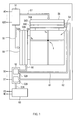
- FIG. 1 is a conceptual diagram showing a general configuration of a magnetic memory device in the embodiment.
- the magnetic memory device of the embodiment has an address buffer 51, a data buffer 52, a control logic part 53, a memory cell group 54, a first drive control circuit part 56, a second drive control circuit part 58, external address input terminals A0 to A20, and external data terminals D0 to D7.
- the memory cell group 54 has a matrix structure in which a number of memory cells 1 each having a pair of tunneling magneto-resistive elements (hereinbelow, called TMR elements) are arranged in a word line direction (X-direction) and a bit line direction (Y-direction) which are orthogonal to each other.
- the memory cell 1 is the minimum unit for storing data in the magnetic memory device and is a concrete example corresponding to a "magnetic memory cell" in the invention. The memory cell 1 will be described in detail later.
- the first drive control circuit part 56 has an address decoder circuit 56A, a sense amplification circuit 56B, and a current drive circuit 56C in the Y-direction.
- the second drive control circuit part 58 has an address decoder circuit 58A, a constant current circuit 58B, and a current drive circuit 58C in the X-direction.
- the address decoder circuits 56A and 58A are to select a word decode line 72 (which will be described later) and a bit decode line 71 (which will be described later) according to an input address signal.
- the Y-direction sense amplification circuit 56B and the X-direction constant current circuit 58B are circuits driven at the time of performing reading operation.
- the Y-direction and X-direction current drive circuits 56C and 58C are circuits driven at the time of performing writing operation.
- the Y-direction sense amplification circuit 56B and the memory cell group 54 are connected to each other via a plurality of bit decode lines 71 in which the sense current flows at the time of reading operation.
- the X-direction constant current circuit 58B and the memory cell group 54 are connected to each other via a plurality of word decode lines 72 in which the sense current flows at the time of reading operation.
- the Y-direction current drive circuit 56C and the memory cell group 54 are connected to each other via write bit lines 5 (which will be described later) necessary at the time of writing operation.
- the X-direction current drive circuit 58C and the memory cell group 54 are connected to each other via write word lines 6 (which will be described later) necessary at the time of writing operation.
- the address buffer 51 has the external address input terminals A0 to A20 and is connected to the Y-direction address decoder circuit 56A in the first drive control circuit part 56 via a Y-direction address line 57 and to the X-direction address decoder circuit 58A in the second drive control circuit part 58 via an X-direction address line 55.
- the address buffer 51 receives an address signal from the outside via the external address input terminals A0 to A20 and amplifies the address signal to a voltage level required in the Y-direction address decoder circuit 56A and the X-direction address decoder circuit 58A by a buffer amplifier (not shown) provided in the address buffer 51.
- the address buffer 51 functions to divide the amplified address signal into two signals and output the signals to the Y-direction address decoder circuit 56A via the Y-direction address line 57 and to the X-direction address decoder circuit 58A via the X-direction address line 55.
- the data buffer 52 is constructed by an input buffer 52A and an output buffer 52B, has the external data terminals D0 to D7, is connected to the control logic part 53, and operates by an output control signal 53A from the control logic part 53.
- the input buffer 52A is connected to the Y-direction current drive circuit 56C in the first drive control circuit part 56 and the X-direction current drive circuit 58C in the second drive control circuit part 58 via a Y-direction write data bus 61 and an X-direction write data bus 60, respectively.
- the input buffer 52A functions to receive signal voltages of the external data terminals D0 to D7, amplify the signal voltage to a required voltage level by an internal buffer amplifier (not shown), and transmit the resultant voltage to the X-direction current drive circuit 58C and the Y-direction current drive circuit 56C via the X-direction write data bus 60 and the Y-direction write data bus 61, respectively.
- the output buffer 52B is connected to the sense amplification circuit 56B via a Y-direction read data bus 62.
- the output buffer 52B functions to amplify the information signal supplied from the sense amplification circuit 56B by an internally provided buffer amplifier (not shown) and to output the resultant signal with low impedance to the external data terminals D0 to D7.
- the control logic part 53 has a chip select terminal CS and a write enable terminal WE and is connected to the data buffer 52.
- the control logic part 53 functions to receive a signal voltage from the chip select terminal CS for selecting a memory cell to be subject to reading/writing from the group 54 of memory cells and a signal voltage from the write enable terminal WE for outputting a write permit signal and to output the output control signal 53A to the data buffer 52.
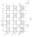
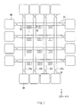
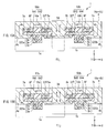
- FIG. 2 is a conceptual diagram showing a configuration in plan view of a main part related to the writing operation in the memory cell group 54.
- the magnetic memory device of the embodiment includes a plurality of write bit lines 5a and 5b and a plurality of write word lines 6 extending so as to cross the plurality of write bit lines 5a and 5b.
- Each region where the write bit lines 5a and 5b and the write word line 6 cross each other includes a parallel part 10a in which the write bit line 5a and the write word line 6 extend parallel with each other and a parallel part 10b in which the write bit line 5b and the write word line 6 extend parallel with each other.
- FIG. 10a in which the write bit line 5a and the write word line 6 extend parallel with each other
- FIG. 10b in which the write bit line 5b and the write word line 6 extend parallel with each other.
- the write word lines 6 extend in the X-direction in a rectangular wave shape and the write bit lines 5a and 5b extend in the Y-direction alternately and linearly.
- the rising and falling portions of the rectangular wave shape of the write word lines 6 form the plurality of parallel parts 10a and 10b in cooperation with the write bit lines 5a and 5b.
- the memory cell 1 is provided in each of the regions where the write bit lines 5a and 5b cross the write word line 6 so as to include at least a part of the parallel parts 10a and 10b.
- the memory cell 1 is constructed by TMR elements 1a and 1b, the TMR element 1a is provided in a region where the write bit line 5a and the write word line 6 cross each other, and the other TMR element 1b is provided in the region where the write bit line 5b and the write word line 6 cross each other.
- the TMR elements 1a and 1b are a concrete example of "a pair of magneto-resistive elements" of the invention.
- the direction of current in the write bit line 5b and that in the write word line 6 flowing in the other TMR element 1b are also parallel with each other.
- the write bit lines 5a and 5b will be simply referred to as the write bit lines 5.
- the write word line 6 is a concrete example corresponding to a "first write line” of the invention
- the write bit line 5 is a concrete example corresponding to a "second write line” of the invention.
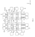
- FIG. 3 shows the configuration in plan view of the main part of the memory cell group 54 more specifically.
- the write bit lines 5a and 5b, write word lines 6, and memory cells 1 (TMR elements 1a and 1b) shown in FIG. 3 correspond to those in FIG. 2.
- the TMR elements 1a and 1b are disposed in the parallel parts 10a and 10b of the write bit lines 5a and 5b and the write word lines 6.
- the TMR elements 1a and 1b have stacked bodies S20a and S20b each including a magneto-sensitive layer and the magnetic yokes 4a and 4b, respectively, and the magnetization direction of the magneto-sensitive layer changes according to the magnetic field generated by the currents flowing in the write bit lines 5a and 5b and the write word lines 6 in the parallel parts 10a and 10b (that is, the external magnetic field in the magnetic yokes 4a and 4b).
- the write word line 6 includes two parts of a part of a first level 6F provided in the same layer (first level L1 which will be described later) as that of the write bit lines 5a and 5b and a part of a second level 6S which is different from the part of the first level 6F and is formed in the second level L2 (to described later).
- the parts of the first and second levels 6F and 6S are electrically connected to each other via a connection layer 6T (which will be described later) made of a conductive material such as aluminum (Al) or copper (Cu).
- the write word line 6 extends in the X-direction over the write bit lines 5a and 5b extending in the Y-direction and functions as a single conductive line extending in the X-direction as a whole.
- the write bit lines 5a and 5b and the part of the first level 6F are provided in the first level L1 in the parallel parts 10a and 10b and are electrically insulated from each other.
- write bit line lead electrodes 47 are provided. One of the write bit line lead electrodes 47 is connected to the Y-direction current drive circuit 56C and the other one is connected so as to be finally grounded. Similarly, write word line lead electrodes 46 are provided at both ends of each write word line 6. One of the write word line lead electrodes 46 is connected to the X-direction current drive circuit 58C and the other one is connected so as to be finally grounded.
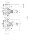
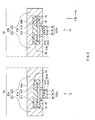
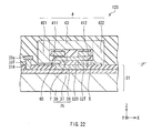
- FIG. 4 is an enlarged perspective view of the memory cell 1.
- FIG. 5 shows a schematic sectional configuration of the memory cell 1, which is taken along line V-V of FIG. 3.
- FIG. 6 shows that the memory cell 1 in FIG. 5 is conceptually divided into the TMR elements 1a and 1b.
- FIGs. 5 and 6 are schematic views for clarifying the detailed configuration. The size ratio and shape of the memory cell 1 in FIGs. 5 and 6 do not always coincide with those of FIG. 4.
- the memory cell 1 has the pair of TMR elements 1a and 1b having magnetic yokes 4a and 4b and stacked bodies S20a and S20b, respectively.
- the write bit lines 5a and 5b and the write word line 6 are arranged so as to be adjacent to each other in the first level L1 parallel with the layer stack face of the stacked bodies S20a and S20b in a region surrounded by the magnetic yokes 4a and 4b (FIG. 5).
- the write word line 6 (part of first level 6F), write bit lines 5a and 5b and magnetic yokes 4a and 4b are electrically insulated from each other via insulating films 7a and 7b.
- the stacked body S20a is disposed in a gap in the magnetic yoke 4a so that a pair of end faces K20a (K21 and K22) face a pair of open ends K4a (K41 and K42). Between the pair of end faces K20a and the pair of open ends K4a, an insulating layer (not shown) made of, for example, aluminum oxide (Al 2 O 3 ) is formed. Similarly, the stacked body S20b is disposed in a gap in the magnetic yoke 4b so that a pair of end faces K20b (K23 and K24) face a pair of open ends K4b (K43 and K44).
- an insulating layer (not shown) made of, for example, aluminum oxide (Al 2 O 3 ) is formed.
- the pair of stacked bodies S20a and S20b is sandwiched between a projection 32T and conductive layers 36a and 36b (which will be described later) and is electrically connected to the conductive layers 36a and 36b in the layer stack direction (Z direction).
- the pair of conductive layers 36a and 36b is a part of a pair of Schottky diodes 75a and 75b (which will be described later) and the other ends of the Schottky diodes 75a and 75b are connected to read bit lines 33a and 33b (which will be described later) extending in the Y-direction.
- the Schottky diodes 75a and 75b are buried in a substrate 31 (which will be described later).
- the surface opposite to the surface which is in contact with the pair of conductive layers 36a and 36b, of the stacked bodies S20a and S20b, that is, the surface on the side of the region surrounded by the magnetic yokes 4a and 4b is in contact with the projection 32T extending in the Y-direction.
- the projection 32T is a part of a read word line 32 extending in the X-direction. Although the projection 32T is in contact with the magnetic yokes 4a and 4b in FIG. 5, they may be electrically insulated from each other via an insulating film.
- the write word line 6 (part of first level 6F) and the write bit lines 5a and 5b are electrically insulated from the read word line 32 (projection 32T).
- the TMR element 1a in the memory cell 1 has: the magnetic yoke 4a disposed in the circumferential direction so as to surround the periphery of the write bit line 5a and the part of the first level 6F in a partial area in the extending direction of the write bit line 5a and the write word line 6, specifically, an area (parallel part 10a) where the write bit line 5a and the write word line 6 extend parallel to each other, and having the pair of open ends K4a (K41 and K42) facing each other over a gap provided in a part of the circumferential direction; and the stacked body S20a including a second magnetic layer 8a as a magneto-sensitive layer of which magnetization direction changes according to an external magnetic field and constructed so that current flows in the direction perpendicular to the stacked face.
- the pair of open ends K4a is provided so as to face each other over the stacked body S20a in the X-direction.
- the other TMR element 1b has: the magnetic yoke 4b disposed in the circumferential direction so as to surround the periphery of the write bit line 5b and the part of the first level 6F in a partial area in the extending direction of the write bit line 5b and the write word line 6, specifically, an area (parallel part 10b) where the write bit line 5b and the write word line 6 extend parallel to each other, and having the pair of open ends K4b (K43 and K44) facing each other over a gap provided in a part of the circumferential direction; and the stacked body S20b including a second magnetic layer 8b as a magneto-sensitive layer of which magnetization direction changes according to an external magnetic field and constructed so that current flows in the direction perpendicular to the stacked face.
- the pair of open ends K4b is provided so as to face each other over the stacked body S20b in the X-direction.
- the TMR elements 1a and 1b share a common part 34 as a part of the magnetic yokes 4a and 4b.
- the stacked bodies S20a and S20b are TMR films including, in order from the side of the write bit line 5 and the write word line 6, the second magnetic layers 8a and 8b, tunnel barrier layers 3a and 3b, and first magnetic layers 2a and 2b whose magnetization direction is fixed, respectively, and constructed so that current flows in the direction perpendicular to the stack layer face.
- the stacked bodies S20a and S20b are exaggerated so as to be larger relative to the peripheral parts.
- the directions of return magnetic fields formed so as to pass in the pair of magnetic yokes 4a and 4b by the write bit lines 5a and 5b and the write word line 6 become the same in the common part 34, and the magnetic flux density increases. Consequently, the return magnetic field can be used more efficiently, and the current necessary to invert the magnetization directions of the magnetic yokes 4a and 4b and the second magnetic layers 8a and 8b can be further decreased. Since a part of the magnetic yoke 4 is shared, the pair of TMR elements 1a and 1b can be easily formed, the formation area of the memory cell 1 can be reduced, and capacity of stored information can be increased.
- the stacked bodies S20a and S20b when a voltage is applied in the direction perpendicular to the layer stack face between the first magnetic layers 2a and 2b and the second magnetic layers 8a and 8b, for example, electrons in the first magnetic layers 2a and 2b pass through the tunnel barrier layers 3a and 3b and move to the second magnetic layers 8a and 8b, and tunnel current flows.
- the tunnel current changes according to a relative angle between the spin in the first magnetic layers 2a and 2b in the interface with the tunnel barrier layer 3 and the spin in the second magnetic layers 8a and 8b. Specifically, when the spin of the first magnetic layers 2a and 2b and that of the second magnetic layers 8a and 8b are parallel to each other, the resistance value becomes the minimum.
- MR ratio magneto-resistance change ratio
- tunnel resistance Rt The resistance value against the tunnel current (hereinbelow, called tunnel resistance Rt) strongly depends on the thickness T of the tunnel barrier layer 3.
- the tunnel resistance Rt exponentially increases with the thickness T of the tunnel barrier layer 3.
- ⁇ denotes the height of the barrier
- m* denotes effective mass of electrons
- Ef indicates Fermi energy
- h indicates a Planck's constant.
- the proper tunnel resistance Rt is about tens k ⁇ ⁇ ( ⁇ m) 2 .
- the tunnel resistance Rt is set to, preferably, 10 k ⁇ ⁇ ( ⁇ m) 2 or less, more preferably, 1k ⁇ ⁇ ( ⁇ m) 2 or less. Therefore, to realize the tunnel resistance Rt, it is desirable to set the thickness T of the tunnel barrier layer 3 to 2 nm or less, more preferably, 1.5 nm or less.
- the tunnel resistance Rt can be reduced but on the other hand, a leak current occurs due to roughness of the junction interfaces with the first magnetic layers 2a and 2b and the second magnetic layers 8a and 8b so that the MR ratio deteriorates.
- the thickness T of the tunnel barrier layers 3a and 3b has to be large to an extent that leak current does not flow. Concretely, the thickness T is desirably 0.3 nm or larger.
- the stacked bodies S20a and S20b have a coercive force differential structure and the coercive force of the first magnetic layers 2a and 2b is larger than that of the second magnetic layers 8a and 8b.
- the coercive force of the first magnetic layer 2 is preferably larger than (50/4 ⁇ )x10 3 A/m, more preferably, (100/4 ⁇ ) ⁇ 10 3 A/m.
- the first magnetic layers 2a and 2b are made of, for example, cobalt iron alloy (CoFe) and have a thickness of 5 nm.
- cobalt (Co), cobalt platinum alloy (CoPt), nickel iron cobalt alloy (NiFeCo), or the like can be applied to the first magnetic layers 2a and 2b.
- the second magnetic layers 8a and 8b are made of, for example, cobalt (Co), cobalt iron alloy (CoFe), cobalt platinum alloy (CoPt), nickel iron alloy (NiFe), or nickel iron cobalt alloy (NiFeCo).
- the axes of easy magnetization of the first magnetic layers 2a and 2b and the second magnetic layers 8a and 8b are preferably parallel to each other so that the magnetization direction of the first magnetic layers 2a and 2b and that of the second magnetic layers 8a and 8b are stabilized in a parallel or antiparallel state.
- the magnetic yokes 4a and 4b extend so as to annularly surround at least a part of the parallel parts 10a and 10b in the write bit lines 5a and 5b and the write word line 6 and are constructed so that a return magnetic field passing in the magnetic yokes 4a and 4b is generated by current flowing in the parallel parts 10a and 10b. More specifically, as shown in FIG.
- the magnetic yoke 4a includes: a pair of facing yokes 41a (411 and 412) extending from the pair of open ends K4a (K41 and K42) and facing each other while sandwiching a gap; a pair of pillar yokes 42a (421 and 422) connected to one ends on the side opposite to the open ends K41 (K41 and K42), of the pair of facing yokes 41a (411 and 412) and extending in the layer stacking direction (Z direction) of the stacked body S20a while facing each other; and a beam yoke 43a connected to one ends on the side opposite to the pair of facing yokes 41a (411 and 412), of the pair of pillar yokes 42a (421 and 422).
- the other magnetic yoke 4b includes: a pair of facing yokes 41b (413 and 414) extending from the pair of open ends K4b (K43 and K44) and facing each other while sandwiching a gap; a pair of pillar yokes 42b (422 and 423) connected to one ends on the side opposite to the open ends K4b (K43 and K44), of the pair of facing yokes 41b (413 and 414) and extending in the layer stacking direction (Z direction) of the stacked body S20b while facing each other; and a beam yoke 43b connected to one ends on the side opposite to the pair of facing yokes 41b (413 and 414), of the pair of pillar yokes 42b (422 and 423).
- the second magnetic layer 8b in the stacked body S20b is in the same level as that of the pair of facing yokes 41b (413 and 414).
- the TMR elements 1a and 1b share the pillar yoke 422, and the common part 34 is formed as shown in FIG. 5.
- the beam yokes 43a and 43b are provided in the second level L2 as that of the part of the second level 6S.
- the magnetization direction of each of such magnetic yokes 4a and 4b is inverted by the return magnetic field generated so as to pass the inside of the magnetic yokes 4a and 4b.
- the magnetization direction of the second magnetic layers 8a and 8b is inverted, so that the second magnetic layers 8a and 8b function as storage layers for storing information.
- the magnetic yokes 4a and 4b are made of, for example, a metal containing at least one of nickel (Ni), iron (Fe), and cobalt (Co).
- the area of the cross section orthogonal to the circumference direction in the magnetic yokes 4a and 4b is the smallest in the pair of open ends K4a and K4b.
- the width in the Y-direction of the pair of facing yokes 41a and 41b in the magnetic yokes 4a and 4b decreases toward the stacked bodies S20a and S20b and becomes the minimum in the pair of open ends K4a and K4b.
- the magnetic permeability of the magnetic yokes 4a and 4b is preferably high to make the return magnetic field generated by the write bit lines 5a and 5b and the write word line 6 concentrated on the magnetic yokes 4a and 4b.
- the magnetic permeability is 2,000 or higher and, more preferably, 6,000 or higher.
- Each of the write bit lines 5a and 5b and the part of the first level 6F has a structure in which a film of titanium (Ti) having a thickness of 10 nm, a film of titanium nitride (TiN) having a thickness of 10 nm, and a film of aluminum (Al) having a thickness of 500 nm are sequentially stacked.
- the part of the second level 6S and the connection layer 6T are made of the same kind of material as that of the magnetic yokes 4a and 4b, for example, NiFe.
- the write bit line 5 and the write word line 6 are not limited to the configuration described above but may be made of at least one of, for example, aluminum (Al), copper (Cu), and tungsten (W). The details of the operation of writing information to the memory cell 1 by using the write bit line 5 and the write word line 6 will be described later.
- the magnetic memory device of the embodiment has a simpler configuration in the layer stacking direction.
- the stacked body S20a is disposed in the gap of the magnetic yoke 4a so that the pair of end faces K20a and the pair of open ends K4a face each other and, similarly, the stacked body S20b is disposed in the gap of the magnetic yoke 4b so that the pair of end faces K20b and the pair of open ends K4b face each other.
- the stacked bodies S20a and S20b fully displaying the magnetic characteristics of the TMR elements 1a and 1b while having the magnetic yokes 4a and 4b as a closed magnetic circuit through which the return magnetic field passes can be obtained.
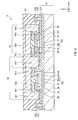
- FIG. 7 is a plan view showing the configuration of a main part related to the reading operation of the memory cell group 54 and corresponds to FIG. 3.
- FIG. 8 is a cross section taken along line XIII-XIII of FIG. 7.
- each memory cell 1 is disposed at a position corresponding to each of the intersecting points of the plurality of read word lines 32 and the plurality of read bit lines 33a and 33b in the XY plane.
- the under face of the stacked bodies S20a and S20b in the memory cell 1 is in contact with the pair of read bit lines 33a and 33b via the pair of Schottky diodes 75a and 75b (hereinbelow, simply called diodes 75a and 75b), and the top face of the stacked bodies S20a and S20b is in contact with the read word line 32.
- the read bit lines 33a and 33b supply read current to the pair of TMR elements 1a and 1b in each memory cell 1 and the read word line 32 leads the read current passed to the TMR elements 1a and 1b to the ground. At both ends of each read bit line 33, read bit line lead electrodes 49 are provided. On the other hand, at both ends of each read word line 32, read word line lead electrodes 48 are provided.
- the magnetic memory device of the embodiment is constructed so that, in a region including the memory cell 1, a pair of stacked bodies S20a and S20b and the magnetic yokes 4a and 4b each having a pair of open ends facing each other while sandwiching the stacked body are formed over the substrate 31 provided with the pair of diodes 75a and 75b functioning as a rectifier.
- the pair of diodes 75a and 75b have the conductive layers 36a and 36b, an epitaxial layer 37, and a substrate 38 in order from the side of the stacked bodies S20a and S20b. Between the conductive layers 36a and 36b and the epitaxial layer 37, a Schottky barrier is formed. The conductive layers 36a and 36b are in contact with the stacked bodies S20a and S20b in a part of the face opposite to the epitaxial layer 37, and the other part is surrounded by insulating layers 31A and 17.
- the diodes 75a and 75b do not have parts electrically connected to each other except for connection to the magnetic layers 4a and 4b while sandwiching the stacked bodies S20a and S20b.
- the substrate 38 is an n type silicon wafer. Generally, in the n type silicon wafer, an impurity of phosphorus (P) is diffused. As the substrate 38, a wafer of an n ++ type obtained by being highly doped with phosphorus is used. As the epitaxial layer 37, a wafer of the n ⁇ type obtained by being lightly doped with phosphorus is used. By making the epitaxial layer 37 as an n ⁇ type semiconductor and the conductive layers 36a and 36b made of a metal come into contact with each other, a band gap is created and a Schottky barrier is formed. Further, the pair of diodes 75a and 75b is connected to the read bit lines 33a and 33b, respectively, via a connection layer 33T.
- P phosphorus
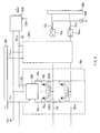
- FIG. 9 the circuit configuration related to the reading operation in the magnetic memory device of the embodiment will be described.
- FIG. 9 is a configuration diagram of a circuit system constructed by the memory cell group 54 and a read circuit.
- the memory cell 1 is of a differential amplifier type constructed by the pair of TMR elements 1a and 1b.
- Information in the memory cell 1 is read by outputting a differential value of read currents passed to the TMR elements 1a and 1b (currents passed from the read bit lines 33a and 33b to the TMR elements 1a and 1b and output to the common read word line 32).
- a unit read circuit 80 (..., 80n, 80n+1, 7) as a unit of repetition of the read circuit is constructed by the memory cells 1 of each bit line in the memory cell group 54 and a part of the read circuit including the sense amplification circuit 56B, and the unit read circuits 80n are arranged in the bit line direction.
- Each of the unit read circuits 80n is connected to the Y-direction address decoder circuit 56A via the bit decode line 71 (..., 71n, 71n+1, ...) and is connected to the output buffer 52B via the Y-direction read data bus 62.
- the read word lines 32 (..., 32m, 32m+1, ...) arranged in the X-direction and the pair of read bit lines 33a and 33b arranged in the Y-direction are disposed in a matrix.
- Each of the memory cells 1 is disposed at a position intersecting with the read word line 32 in a region sandwiched by the pair of read bit lines 33a and 33b.
- One ends of the TMR elements 1a and 1b in each memory cell 1 are connected to the read bit lines 33a and 33b via the pair of diodes 75a and 75b, respectively, and the other ends are connected to the common read word line 32.
- each read word line 32 is connected to a read switch 83 (..., 83 m , 83 m+1 , ...) via the read word line lead electrode 48 and is also connected to a common X-direction constant current circuit 58B.
- Each read switch 83 is connected to the X-direction address decoder circuit 58A via the word decode line 72 (..., 72 m , 72 m+1 , ).
- the read switch 83 is made conductive when a selection signal from the X-direction address decoder circuit 58A is supplied.
- the X-direction constant current circuit 58B has the function of making the current flowing in the read word line 32 constant.
- each read bit line 33 is connected to the Y-direction sense amplification circuit 56B via the read bit line lead electrode 49, and the other end is finally grounded.
- One Y-direction sense amplification circuit 56B is provided per unit read circuit 80 and has the function of receiving the potential difference between the pair of read bit lines 33a and 33b in each unit read circuit 80 and amplifying the potential difference.
- the Y-direction sense amplification circuit 56B is connected to the output line 82 (..., 82n, 82n+1, ...) and is finally connected to the output buffer 52B via the Y-direction read data bus 62.
- FIGs. 10A and 10B express the relation between the write current direction and the return magnetic field direction (magnetization direction) in the cross-sectional configuration of the memory cell 1 shown in FIG. 5.
- the arrows indicated in magnetic layers in FIGs. 10A and 10B indicate the magnetization directions of the magnetic layers.
- the magnetic yokes 4a and 4b the magnetic field directions of a magnetic path formed on the inside are also shown.
- the magnetization of the first magnetic layers 2a and 2b is fixed to the -X direction.
- FIG. 10A and 10B show the case where write current flows in the same direction to the write bit line 5 and the part of the first level 6F which extend in the memory cell 1 and are parallel to each other.
- FIG. 10A corresponds to the write current direction shown in FIG. 2.
- FIG. 10A shows a case where write current flows from this side to the depth in the direction perpendicular to the drawing sheet (to the +Y direction) in the TMR element 1a, a return magnetic field 16a is generated in the clockwise direction so as to pass the inside of the magnetic yoke 4a surrounding the write bit line 5a and the part of the first level 6F, write current flows from the depth to this in the direction perpendicular to the drawing sheet side (to the ⁇ Y direction) in the TMR element 1b, and a return magnetic field 16b is generated in the counterclockwise direction so as to pass the inside of the magnetic yoke 4b surrounding the write bit line 5b and the part of the first level 6F.
- FIG. 10B corresponds to the case where the directions of current flowing in the write bit line 5 and the part of the first level 6F are opposite to those shown in FIG. 10A. Specifically, FIG.
- the 10B shows a case where write current flows from the depth to this side in the direction perpendicular to the drawing sheet (to the -Y direction) in the TMR element 1a, the return magnetic field 16a is generated in the counterclockwise direction so as to pass the inside of the magnetic yoke 4a surrounding the write bit line 5a and the part of the first level 6F, write current flows from this side to the depth in the direction perpendicular to the drawing sheet (to the +Y direction) in the TMR element 1b, and the return magnetic field 16b is generated in the clockwise direction so as to pass the inside of the magnetic yoke 4b surrounding the write bit line 5b and the part of the first level 6F.
- the magnetization direction of the second magnetic layer 8a is the +X direction
- the magnetization direction of the second magnetic layer 8b is the -X direction.
- the magnetization direction of the second magnetic layer 8a and that of the second magnetic layer 8b change so as to be opposite to each other.
- information can be stored in the memory cell 1.
- the magnetization directions of the magnetic yokes 4a and 4b are inverted and, accompanying the inversion, the magnetization directions of the second magnetic layers 8a and 8b change, thereby enabling binary information of "0" or "1" to be stored.
- "0" corresponds to, for example, the state of FIG. 10A, specifically, the state where the second magnetic layer 8a is magnetized in the -X direction and the other second magnetic layer 8b is magnetized in the +X direction
- "1" corresponds to the state of FIG. 10B, specifically, the state where the second magnetic layer 8a is magnetized in the +X direction and the second magnetic layer 8b is magnetized in the -X direction. In such a manner, information can be stored.
- the TMR elements 1a and 1b when the magnetization direction of the first magnetic layers 2a and 2b and that of the second magnetic layers 8a and 8b are parallel, a low resistance state in which large tunnel current flows is obtained. When they are antiparallel to each other, a high resistance state in which only small tunnel current flows is obtained. That is, one of the pair of TMR elements 1a and 1b is always in the low resistance state and the other one is in the high resistance state, thereby storing information.
- the current magnetic field can be used more efficiently and the current necessary to invert the magnetization in the second magnetic layers 8a and 8b can be reduced.
- the pair of open ends K4a faces the pair of end faces K20a
- the pair of open ends K4b faces the pair of end faces K20b. Consequently, the stack bodies S20a and S20b are disposed in the closed magnetic circuit formed in the magnetic yokes 4a and 4b by passing current to both of the write bit lines 5a and 5b and the write word line 6. Therefore, magnetization inversion in the magnetic yokes 4a and 4b in the TMR elements 1a and 1b can be performed more efficiently and a magnetic influence on memory cells adjacent to the memory cell 1 to be subject to writing can be reduced.
- the second magnetic layer 8a is disposed so as to be in the same level as the pair of facing yokes 411 and 412 and the second magnetic layer 8b is disposed so as to be in the same level as the pair of facing yokes 413 and 414. Consequently, the magnetic flux density of the return magnetic fields passing the second magnetic layers 8a and 8b becomes higher and magnetization inversion in the second magnetic layers 8a and 8b can be performed more efficiently.
- one of the plurality of bit decode lines 71 is selected by the Y-direction address decoder circuit 56A in the first drive control circuit part 56 and a control signal is transmitted to the corresponding Y-direction sense amplification circuit 56B.
- read current flows in the read bit lines 33a and 33b and the positive potential is given to the side of the stacked bodies S20a and S20b in the TMR elements 1a and 1b.
- the X-direction address decoder circuit 58A in the second drive control circuit part 58 one of the plurality of word decode lines 72 is selected and the read switch 83 in the corresponding part is driven.
- the selected read switch 83 is energized, read current flows in the corresponding read word line 32, and a negative potential is given to the side opposite to that of the stacked bodies S20a and S20b. Therefore, read current necessary for reading can be passed to one memory cell 1 selected by the Y-direction address decoder circuit 56A and the X-direction address decoder circuit 58A. Based on the read current, the magnetization directions of the pair of second magnetic layers 8a and 8b are detected, thereby enabling stored information to be read.
- FIGs. 11A and 11B are circuit diagrams each showing a portion around the memory cell 1.
- the magnetization directions of the first magnetic layers 2a and 2b in the stacked bodies S20a and S20b are indicated by hollow arrows and those of the second magnetic layers 8a and 8b are indicated by solid arrows. Both of the magnetization directions of the first magnetic layers 2a and 2b are fixed to the left directions.
- the magnetization direction of the first magnetic layer 2a and that in the second magnetic layer 2b in the stacked body S20a are parallel, and the magnetization direction of the first magnetic layer 2b and that of the second magnetic layer 2b in the other stacked body S20b are antiparallel to each other.
- the stacked body S20a is in the low resistance state, and the stacked body S20b is in the high resistance state.
- This case corresponds to, for example, "0".
- the stacked body S20a is in the high resistance state and the stacked body S20b is in the low resistance state.
- This case corresponds to, for example, "1”.
- Such binary information can be obtained by utilizing the fact that the resistance values of the stacked bodies S20a and S20b are different from each other and detecting the difference between the values of currents flowing in the stacked bodies S20a and S20b.
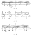
- the method of manufacturing the magnetic memory device of the embodiment includes: a stacked body forming step of forming the pair of stacked bodies S20a and S20b over the substrate 31 provided with the pair of diodes 75a and 75b; a bottom yoke forming step of forming bottom yokes 4B so as to face each other while sandwiching each of the pair of stacked bodies S20a and S20b; a write line forming step of simultaneously forming the pair of parts of the first level 6F and the write bit lines 5a and 5b so as to be disposed adjacent to each other in the first level L1 including the same plane parallel to the layer stack face of the stacked bodies S20a and S20b via the read word line 32 (projection 32T) and an insulating film 7A over the bottom yoke 4B; and a magnetic yoke forming step of forming the pair of magnetic yokes 4a and 4b which are disposed in the circumferential direction so as to surround the pair of write word lines 6B and the write bit lines 5
- FIGs. 12 to 19 are cross sections taken along line ⁇ - ⁇ '- ⁇ shown in FIG. 3 and show manufacturing processes in order. Although only the TMR 1a in the memory cell 1 is shown and the TMR 1b is not shown in FIGs. 12 to 19, the manufacturing method forms the TMRs 1a and 1b simultaneously.
- the bottom yoke 4B (specifically, the facing yokes 41a and 41b and part of pillar yokes 421 to 423) is formed over the substrate 31 so as to face each other while sandwiching each of the stacked bodies S20a and S20b.
- the substrate 31 in which the diodes 75a and 75b are buried and on which the stacked bodies S20a and S20b and the insulating film 17A surrounding the stacked bodies S20a and S20b and the periphery of the stacked bodies S20a and S20b are formed is prepared.
- FIGs. 13 to 19 following FIG. 12 the details of the substrate 31 will be omitted.
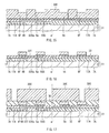
- a resist pattern 30A is selectively formed.
- the resist pattern 30A is used as a mask and the insulating film 17A in not-protected regions is etched to at least a depth corresponding to the thickness of the second magnetic layers 8a and 8b in the stacked bodies S20a and S20b by reactive ion etching (RIE) or the like.
- RIE reactive ion etching
- the bottom yokes 4B facing each other while sandwiching the stacked bodies S20a and S20b are formed by, for example, sputtering to the level which is the same as that of the top face of the stacked bodies S20a and S20b so as to fill in the etched regions in the insulating film 17A.
- the write bit lines 5a and 5b and the parts of the first level 6F are formed so as to be disposed adjacent to each other in the first level L1.
- the read word line 32 projection 32T
- the insulating film 7A and an underplating film 56S are sequentially formed on the whole surface.
- the insulating film 7A made of aluminum oxide (Al 2 O 3 ) or the like is formed and, after that, the underplating film 56S made of a conductive material such as copper (Cu) is formed by sputtering or the like.
- the resist pattern 30B is selectively formed on the underplating film 56S.
- the resist pattern 30B is formed so as not to cover regions in which the write bit lines 5a and 5b and the parts of the first level 6F are to be formed.
- the resultant is soaked in a plating bath and a plating process using the underplating film 56S as an electrode is performed, thereby simultaneously forming the write bit lines 5a and 5b and the parts of the first level 6F.
- the resist pattern 30B is removed and, further, the exposed underplating film 56S is removed by milling or the like.
- a frame plating method such a thin film patterning method is called a frame plating method.
- the top magnetic yoke 4U (specifically, a pair of pillar yokes 42 and a second beam yoke 43) and the parts of the second level 6S are formed.
- the insulating film 7B made of Al 2 O 3 is formed by sputtering or the like on the whole surface and, after that, a resist pattern 30C is selectively formed on the insulating film 7B.
- the resist pattern 30C is formed so as not to cover parts corresponding to parts on both sides of the regions in which the write bit lines 5a and 5b and the parts of the first level 6F are formed in the region where the bottom yoke 4B is formed and parts corresponding to the parts of the first level 6F in the region where the bottom yoke 4B is not formed.
- the resist pattern 30C is used as a mask and the insulating films 7A and 7B in the not-protected regions are removed by reactive ion etching (RIE) or the like.
- the write word line lead electrodes 46 are formed at both ends of the write word line 6
- the write bit line lead electrodes 47 are formed at both ends of the write bit line 5
- the read word line lead electrodes 48 are formed at both ends of the read word line 32 and, further, the read bit line lead electrodes 49 are formed at both ends of the read bit line 33.
- the method of manufacturing the magnetic memory device of the embodiment includes the process of simultaneously forming the write bit lines 5a and 5b and the parts of the first level 6F. Consequently, as compared with the case of forming the write bit lines 5a and 5b and the parts of the first level 6F separately, the memory cell 1 can be formed by the smaller number of processes.
- the magnetic yoke forming step includes the step of forming the part of the second level 6S simultaneously with the top magnetic yoke 4U in regions other than the regions surrounded by the magnetic yokes 4a and 4b, so that the manufacturing process can be further simplified.
- the configuration of the stacked body is not limited to that of the stacked bodies S20a and S20b shown in FIG. 5 in the foregoing embodiment.
- the second magnetic layers 8a and 8b as magneto-sensitive layers may have a two-layer structure including first free magnetization layers 181a and 181b and second free magnetization layers 182a and 182b having a coercive force larger than that of the first free magnetization layers 181a and 181b, respectively.
- the stacked body is not limited to the configuration that current flows in the direction orthogonal to the layer stack face but may be constructed so that current flows along the layer stack face.
- part of the projection 32T in the read word line 32 may also serve as a magneto-sensitive layer of the stacked body.
- connection parts 183a and 183b as part of the projections 32T also function as magneto-sensitive layers in stacked bodies S22a and S22b. Consequently, the second magnetic layers 8a and 8b provided in the TMR elements 1a and 1b in the foregoing embodiment can be omitted and the memory cell 122 having a configuration simpler than that of the memory cell 1 can be obtained.
- it is desirable to form the projection 32T by using, for example, NiFe (permalloy) in consideration of conductivity and a soft magnetic property.
- the magnetic memory cell having the pair of magnetoresistive elements has been described above in the foregoing embodiment, the invention is not limited to the configuration.
- a single TMR element having one magnetic yoke 4 and one stacked body S20 may be used as the magnetic memory device.
Abstract
Description
Claims (16)
- A magneto-resistive element comprising:wherein the stacked body is disposed in the gap so that each of the pair of end faces and each of the pair of open ends face each other.a magnetic yoke disposed annularly, in a partial region along an extension direction of a conductor, in a circumferential direction so as to surround the conductor, and having a pair of open ends facing each other while sandwiching a gap provided in a part in the circumferential direction; anda stacked body including a magneto-sensitive layer of which magnetization direction changes according to an external magnetic field and a pair of end faces,
- A magneto-resistive element according to claim 1,
wherein an insulating layer is provided between each of the pair of end faces and each of the pair of open ends. - A magneto-resistive element according to claim 1, wherein area of a cross section orthogonal to the circumferential direction, of the magnetic yoke is the smallest at the pair of open ends.
- A magneto-resistive element according claim 1, wherein the magnetic yoke includes:a pair of facing yokes extending in a direction apart from the pair of open ends and facing each other while sandwiching the gap;a pair of pillar yokes each connected to one end on the side opposite to the open end, of each of the pair of facing yokes and extending in the layer stack direction of the stacked body while facing each other; anda beam yoke connected to one end on the side opposite to the pair of facing yokes, of each of the pair of pillar yokes.
- A magneto-resistive element according to claim 4, wherein the magneto-sensitive layer is provided at the same level as that of the pair of facing yokes.
- A magnetic memory cell having a pair of magneto-resistive elements each comprising:wherein the stacked body is disposed in the gap so that each of the pair of end faces and each of the pair of open ends face each other.a magnetic yoke disposed annularly, in a partial region along an extension direction of a conductor, in a circumferential direction so as to surround the conductor, and having a pair of open ends facing each other while sandwiching a gap provided in a part in the circumferential direction; anda stacked body including a magneto-sensitive layer of which magnetization direction changes according to an external magnetic field and a pair of end faces,
- A magnetic memory cell according to claim 6,
wherein an insulating layer is provided between each of the pair of end faces and each of the pair of open ends. - A magnetic memory cell according to claim 6, wherein area of a cross section orthogonal to the circumferential direction, of the magnetic yoke is the smallest at the pair of open ends.
- A magnetic memory cell according to claim 6, wherein each of the pair of magnetic yokes includes:a pair of facing yokes extending in a direction apart from the pair of open ends and facing each other while sandwiching the gap;a pair of pillar yokes each connected to one end on the side opposite to the open end, of each of the pair of facing yokes and extending in the layer stack direction of the stacked body while facing each other; anda beam yoke connected to one end on the side opposite to the pair of facing yokes, of each of the pair of pillar yokes, andthe pair of magneto-resistive elements shares at least one of the pair of pillar yokes.
- A magnetic memory cell according to claim 9, wherein the magneto-sensitive layer is provided at the same level as that of the pair of facing yokes.
- A magnetic memory device comprising:wherein each of the pair of magneto-resistive elements has:a first write line;a second write line extended so as to cross the first write line and, in a portion corresponding to an area of intersection with the first write line, extended parallel to the first write line; anda magnetic memory cell including a pair of magneto-resistive elements,a magnetic yoke disposed annularly, in a partial region along an extension direction of the first and second write lines, in a circumferential direction so as to surround the first and second write lines, and having a pair of open ends facing each other while sandwiching a gap provided in a part in the circumferential direction; anda stacked body including a magneto-sensitive layer of which magnetization direction changes according to an external magnetic field and a pair of end faces, andthe stacked body is disposed in the gap so that each of the pair of end faces and each of the pair of open ends face each other.
- A magnetic memory device according to claim 11,
wherein an insulating layer is provided between each of the pair of end faces and each of the pair of open ends. - A magnetic memory device according to claim 11, wherein area of a cross section orthogonal to the circumferential direction, of the magnetic yoke is the smallest at the pair of open ends.
- A magnetic memory device according to claim 11, wherein each of the pair of magnetic yokes includes:a pair of facing yokes extending in a direction apart from the pair of open ends and facing each other while sandwiching the gap;a pair of pillar yokes each connected to one end on the side opposite to the open end, of each of the pair of facing yokes and extending in the layer stack direction of the stacked body while facing each other; anda beam yoke connected to one end on the side opposite to the pair of facing yokes, of each of the pair of pillar yokes, andthe pair of magneto-resistive elements shares at least one of the pair of pillar yokes.
- A magnetic memory device according to claim 14, wherein the magneto-sensitive layer is provided at the same level as that of the pair of facing yokes.
- A magnetic memory device according to claim 11, further comprising a read line electrically connected to the stacked body in a region in which the first and second write lines are surrounded by the magnetic yoke.
Applications Claiming Priority (2)
| Application Number | Priority Date | Filing Date | Title |
|---|---|---|---|
| JP2003361050 | 2003-10-21 | ||
| JP2003361050A JP4438375B2 (en) | 2003-10-21 | 2003-10-21 | Magnetoresistive element, magnetic memory cell, and magnetic memory device |
Publications (3)
| Publication Number | Publication Date |
|---|---|
| EP1528569A2 true EP1528569A2 (en) | 2005-05-04 |
| EP1528569A3 EP1528569A3 (en) | 2005-11-09 |
| EP1528569B1 EP1528569B1 (en) | 2011-08-17 |
Family
ID=34420078
Family Applications (1)
| Application Number | Title | Priority Date | Filing Date |
|---|---|---|---|
| EP04024947A Expired - Fee Related EP1528569B1 (en) | 2003-10-21 | 2004-10-20 | Magnetoresistive element, magnetic memory cell, and magnetic memory device |
Country Status (4)
| Country | Link |
|---|---|
| US (1) | US7002840B2 (en) |
| EP (1) | EP1528569B1 (en) |
| JP (1) | JP4438375B2 (en) |
| CN (1) | CN1610000B (en) |
Cited By (1)
| Publication number | Priority date | Publication date | Assignee | Title |
|---|---|---|---|---|
| EP4145450A1 (en) * | 2021-09-03 | 2023-03-08 | Kioxia Corporation | Magnetic memory |
Families Citing this family (9)
| Publication number | Priority date | Publication date | Assignee | Title |
|---|---|---|---|---|
| JP2005109266A (en) * | 2003-09-30 | 2005-04-21 | Tdk Corp | Magnetic memory device and manufacturing method of magnetic memory device |
| JP2006100423A (en) * | 2004-09-28 | 2006-04-13 | Tdk Corp | Magnetic storage device |
| JP2006100424A (en) * | 2004-09-28 | 2006-04-13 | Tdk Corp | Magnetic storage device |
| JP2006344653A (en) | 2005-06-07 | 2006-12-21 | Toshiba Corp | Magnetic random access memory |
| JP2007059865A (en) * | 2005-07-27 | 2007-03-08 | Tdk Corp | Magnetic storage |
| CN100437817C (en) * | 2005-12-31 | 2008-11-26 | 中国科学院物理研究所 | Magnetic random access storage based on circular magnetic multilayer film and its control method |
| JP5076373B2 (en) * | 2006-06-27 | 2012-11-21 | Tdk株式会社 | Magnetic storage device and magnetic storage method |
| US7782659B2 (en) * | 2007-05-10 | 2010-08-24 | Macronix International Co., Ltd. | Magnetic memory and memory cell thereof and method of manufacturing the memory cell |
| KR102078849B1 (en) * | 2013-03-11 | 2020-02-18 | 삼성전자 주식회사 | Magnetoresistive structure, Magnetic Random Access Memory device and Manufacturing Method of the same |
Citations (4)
| Publication number | Priority date | Publication date | Assignee | Title |
|---|---|---|---|---|
| JPH0293373A (en) | 1988-09-29 | 1990-04-04 | Nippon Denso Co Ltd | Current detector |
| JP2001236781A (en) | 1999-12-16 | 2001-08-31 | Toshiba Corp | Magnetic memory device |
| US20010050859A1 (en) | 1998-08-12 | 2001-12-13 | Siegfried Schwarzl | Memory cell array and method for manufacturing it |
| EP1246191A2 (en) | 2001-03-27 | 2002-10-02 | Kabushiki Kaisha Toshiba | Magnetic memory device |
Family Cites Families (6)
| Publication number | Priority date | Publication date | Assignee | Title |
|---|---|---|---|---|
| US5343422A (en) * | 1993-02-23 | 1994-08-30 | International Business Machines Corporation | Nonvolatile magnetoresistive storage device using spin valve effect |
| US5629922A (en) * | 1995-02-22 | 1997-05-13 | Massachusetts Institute Of Technology | Electron tunneling device using ferromagnetic thin films |
| JP3333670B2 (en) | 1995-09-22 | 2002-10-15 | ティーディーケイ株式会社 | Magnetic thin film memory |
| JP2001273759A (en) | 2000-03-27 | 2001-10-05 | Sharp Corp | Magnetic memory cell and magnetic memory device |
| JP2003174149A (en) * | 2001-12-07 | 2003-06-20 | Mitsubishi Electric Corp | Magnetoresistive memory storage element and magnetic random access memory device |
| JP3906145B2 (en) * | 2002-11-22 | 2007-04-18 | 株式会社東芝 | Magnetic random access memory |
-
2003
- 2003-10-21 JP JP2003361050A patent/JP4438375B2/en not_active Expired - Lifetime
-
2004
- 2004-10-19 US US10/967,297 patent/US7002840B2/en active Active
- 2004-10-20 EP EP04024947A patent/EP1528569B1/en not_active Expired - Fee Related
- 2004-10-21 CN CN2004100877325A patent/CN1610000B/en not_active Expired - Fee Related
Patent Citations (4)
| Publication number | Priority date | Publication date | Assignee | Title |
|---|---|---|---|---|
| JPH0293373A (en) | 1988-09-29 | 1990-04-04 | Nippon Denso Co Ltd | Current detector |
| US20010050859A1 (en) | 1998-08-12 | 2001-12-13 | Siegfried Schwarzl | Memory cell array and method for manufacturing it |
| JP2001236781A (en) | 1999-12-16 | 2001-08-31 | Toshiba Corp | Magnetic memory device |
| EP1246191A2 (en) | 2001-03-27 | 2002-10-02 | Kabushiki Kaisha Toshiba | Magnetic memory device |
Cited By (2)
| Publication number | Priority date | Publication date | Assignee | Title |
|---|---|---|---|---|
| EP4145450A1 (en) * | 2021-09-03 | 2023-03-08 | Kioxia Corporation | Magnetic memory |
| US11871586B2 (en) | 2021-09-03 | 2024-01-09 | Kioxia Corporation | Magnetic memory |
Also Published As
| Publication number | Publication date |
|---|---|
| EP1528569B1 (en) | 2011-08-17 |
| EP1528569A3 (en) | 2005-11-09 |
| CN1610000B (en) | 2010-05-26 |
| CN1610000A (en) | 2005-04-27 |
| JP2005129587A (en) | 2005-05-19 |
| JP4438375B2 (en) | 2010-03-24 |
| US20050117386A1 (en) | 2005-06-02 |
| US7002840B2 (en) | 2006-02-21 |
Similar Documents
| Publication | Publication Date | Title |
|---|---|---|
| EP1511041B1 (en) | Magnetic memory cell and magnetic memory device, and method for manufacturing the same | |
| US20050036376A1 (en) | Magnetic random access memory | |
| JP2004153070A (en) | Magnetic random access memory and its manufacturing method | |
| EP1406266A2 (en) | Magnetic memory and its write/read method | |
| EP1528569B1 (en) | Magnetoresistive element, magnetic memory cell, and magnetic memory device | |
| US7209380B2 (en) | Magnetic memory device and method of reading the same | |
| EP1523011B1 (en) | Magnetoresistive element, magnetic memory cell, and magnetic memory device | |
| JP4729836B2 (en) | Magnetic storage cell, magnetic memory device, and method of manufacturing magnetic memory device | |
| JP4720067B2 (en) | Magnetic storage cell, magnetic memory device, and method of manufacturing magnetic memory device | |
| US7157760B2 (en) | Magnetic memory device and method of manufacturing magnetic memory device | |
| EP1679719B1 (en) | Magnetoresistive element, magnetic memory cell, and magnetic memory device | |
| JP4556385B2 (en) | Method for manufacturing magnetic memory device | |
| JP2006156893A (en) | Magnetic memory |
Legal Events
| Date | Code | Title | Description |
|---|---|---|---|
| PUAI | Public reference made under article 153(3) epc to a published international application that has entered the european phase |
Free format text: ORIGINAL CODE: 0009012 |
|
| AK | Designated contracting states |
Kind code of ref document: A2 Designated state(s): AT BE BG CH CY CZ DE DK EE ES FI FR GB GR HU IE IT LI LU MC NL PL PT RO SE SI SK TR |
|
| AX | Request for extension of the european patent |
Extension state: AL HR LT LV MK |
|
| PUAL | Search report despatched |
Free format text: ORIGINAL CODE: 0009013 |
|
| AK | Designated contracting states |
Kind code of ref document: A3 Designated state(s): AT BE BG CH CY CZ DE DK EE ES FI FR GB GR HU IE IT LI LU MC NL PL PT RO SE SI SK TR |
|
| AX | Request for extension of the european patent |
Extension state: AL HR LT LV MK |
|
| 17P | Request for examination filed |
Effective date: 20060322 |
|
| AKX | Designation fees paid |
Designated state(s): DE FR GB |
|
| 17Q | First examination report despatched |
Effective date: 20071129 |
|
| GRAP | Despatch of communication of intention to grant a patent |
Free format text: ORIGINAL CODE: EPIDOSNIGR1 |
|
| GRAS | Grant fee paid |
Free format text: ORIGINAL CODE: EPIDOSNIGR3 |
|
| GRAA | (expected) grant |
Free format text: ORIGINAL CODE: 0009210 |
|
| AK | Designated contracting states |
Kind code of ref document: B1 Designated state(s): DE FR GB |
|
| REG | Reference to a national code |
Ref country code: GB Ref legal event code: FG4D |
|
| REG | Reference to a national code |
Ref country code: DE Ref legal event code: R096 Ref document number: 602004033957 Country of ref document: DE Effective date: 20111020 |
|
| PLBE | No opposition filed within time limit |
Free format text: ORIGINAL CODE: 0009261 |
|
| STAA | Information on the status of an ep patent application or granted ep patent |
Free format text: STATUS: NO OPPOSITION FILED WITHIN TIME LIMIT |
|
| 26N | No opposition filed |
Effective date: 20120521 |
|
| GBPC | Gb: european patent ceased through non-payment of renewal fee |
Effective date: 20111117 |
|
| REG | Reference to a national code |
Ref country code: DE Ref legal event code: R097 Ref document number: 602004033957 Country of ref document: DE Effective date: 20120521 |
|
| PG25 | Lapsed in a contracting state [announced via postgrant information from national office to epo] |
Ref country code: GB Free format text: LAPSE BECAUSE OF NON-PAYMENT OF DUE FEES Effective date: 20111117 |
|
| PGFP | Annual fee paid to national office [announced via postgrant information from national office to epo] |
Ref country code: FR Payment date: 20121018 Year of fee payment: 9 Ref country code: DE Payment date: 20121017 Year of fee payment: 9 |
|
| REG | Reference to a national code |
Ref country code: DE Ref legal event code: R119 Ref document number: 602004033957 Country of ref document: DE Effective date: 20140501 |
|
| REG | Reference to a national code |
Ref country code: FR Ref legal event code: ST Effective date: 20140630 |
|
| PG25 | Lapsed in a contracting state [announced via postgrant information from national office to epo] |
Ref country code: DE Free format text: LAPSE BECAUSE OF NON-PAYMENT OF DUE FEES Effective date: 20140501 Ref country code: FR Free format text: LAPSE BECAUSE OF NON-PAYMENT OF DUE FEES Effective date: 20131031 |