EP1528600B1 - Vertical high-voltage transistor - Google Patents
Vertical high-voltage transistor Download PDFInfo
- Publication number
- EP1528600B1 EP1528600B1 EP04078400A EP04078400A EP1528600B1 EP 1528600 B1 EP1528600 B1 EP 1528600B1 EP 04078400 A EP04078400 A EP 04078400A EP 04078400 A EP04078400 A EP 04078400A EP 1528600 B1 EP1528600 B1 EP 1528600B1
- Authority
- EP
- European Patent Office
- Prior art keywords
- regions
- region
- drift
- substrate
- source
- Prior art date
- Legal status (The legal status is an assumption and is not a legal conclusion. Google has not performed a legal analysis and makes no representation as to the accuracy of the status listed.)
- Expired - Lifetime
Links
- 210000000746 body region Anatomy 0.000 claims abstract description 10
- 239000000758 substrate Substances 0.000 claims description 47
- 239000004065 semiconductor Substances 0.000 claims description 24
- VYPSYNLAJGMNEJ-UHFFFAOYSA-N Silicium dioxide Chemical compound O=[Si]=O VYPSYNLAJGMNEJ-UHFFFAOYSA-N 0.000 claims description 18
- 235000012239 silicon dioxide Nutrition 0.000 claims description 9
- 239000000377 silicon dioxide Substances 0.000 claims description 9
- 230000005684 electric field Effects 0.000 claims description 6
- 239000010410 layer Substances 0.000 description 95
- 239000000463 material Substances 0.000 description 14
- 229910021420 polycrystalline silicon Inorganic materials 0.000 description 11
- 238000012545 processing Methods 0.000 description 11
- XUIMIQQOPSSXEZ-UHFFFAOYSA-N Silicon Chemical compound [Si] XUIMIQQOPSSXEZ-UHFFFAOYSA-N 0.000 description 9
- 238000000034 method Methods 0.000 description 9
- 229920005591 polysilicon Polymers 0.000 description 9
- 229910052710 silicon Inorganic materials 0.000 description 9
- 239000010703 silicon Substances 0.000 description 9
- 230000015556 catabolic process Effects 0.000 description 7
- 238000009792 diffusion process Methods 0.000 description 7
- 238000005530 etching Methods 0.000 description 6
- 230000005669 field effect Effects 0.000 description 6
- 238000004519 manufacturing process Methods 0.000 description 6
- 239000002184 metal Substances 0.000 description 6
- 229910052751 metal Inorganic materials 0.000 description 6
- 230000015572 biosynthetic process Effects 0.000 description 5
- 239000004020 conductor Substances 0.000 description 5
- 239000012535 impurity Substances 0.000 description 5
- 238000000151 deposition Methods 0.000 description 4
- 230000000903 blocking effect Effects 0.000 description 3
- 238000007796 conventional method Methods 0.000 description 3
- 230000008021 deposition Effects 0.000 description 3
- 238000000227 grinding Methods 0.000 description 3
- 239000011810 insulating material Substances 0.000 description 3
- 229910021332 silicide Inorganic materials 0.000 description 3
- FVBUAEGBCNSCDD-UHFFFAOYSA-N silicide(4-) Chemical compound [Si-4] FVBUAEGBCNSCDD-UHFFFAOYSA-N 0.000 description 3
- 229910052581 Si3N4 Inorganic materials 0.000 description 2
- 238000013459 approach Methods 0.000 description 2
- 239000003989 dielectric material Substances 0.000 description 2
- 238000009826 distribution Methods 0.000 description 2
- 230000008030 elimination Effects 0.000 description 2
- 238000003379 elimination reaction Methods 0.000 description 2
- 238000002513 implantation Methods 0.000 description 2
- 229910001092 metal group alloy Inorganic materials 0.000 description 2
- -1 n-type) Substances 0.000 description 2
- 238000000059 patterning Methods 0.000 description 2
- HQVNEWCFYHHQES-UHFFFAOYSA-N silicon nitride Chemical compound N12[Si]34N5[Si]62N3[Si]51N64 HQVNEWCFYHHQES-UHFFFAOYSA-N 0.000 description 2
- JCALBVZBIRXHMQ-UHFFFAOYSA-N [[hydroxy-(phosphonoamino)phosphoryl]amino]phosphonic acid Chemical compound OP(O)(=O)NP(O)(=O)NP(O)(O)=O JCALBVZBIRXHMQ-UHFFFAOYSA-N 0.000 description 1
- 239000000969 carrier Substances 0.000 description 1
- 239000002800 charge carrier Substances 0.000 description 1
- 238000006243 chemical reaction Methods 0.000 description 1
- 238000005229 chemical vapour deposition Methods 0.000 description 1
- 230000002939 deleterious effect Effects 0.000 description 1
- 230000001419 dependent effect Effects 0.000 description 1
- 238000001312 dry etching Methods 0.000 description 1
- 238000005516 engineering process Methods 0.000 description 1
- 239000012212 insulator Substances 0.000 description 1
- 239000007788 liquid Substances 0.000 description 1
- 230000000873 masking effect Effects 0.000 description 1
- 229910044991 metal oxide Inorganic materials 0.000 description 1
- 150000004706 metal oxides Chemical class 0.000 description 1
- 238000007747 plating Methods 0.000 description 1
- 238000005498 polishing Methods 0.000 description 1
- 230000002028 premature Effects 0.000 description 1
- 239000002356 single layer Substances 0.000 description 1
- 238000004544 sputter deposition Methods 0.000 description 1
- 239000002344 surface layer Substances 0.000 description 1
- 238000001039 wet etching Methods 0.000 description 1
Images


Classifications
-
- H—ELECTRICITY
- H01—ELECTRIC ELEMENTS
- H01L—SEMICONDUCTOR DEVICES NOT COVERED BY CLASS H10
- H01L29/00—Semiconductor devices adapted for rectifying, amplifying, oscillating or switching, or capacitors or resistors with at least one potential-jump barrier or surface barrier, e.g. PN junction depletion layer or carrier concentration layer; Details of semiconductor bodies or of electrodes thereof ; Multistep manufacturing processes therefor
- H01L29/66—Types of semiconductor device ; Multistep manufacturing processes therefor
- H01L29/68—Types of semiconductor device ; Multistep manufacturing processes therefor controllable by only the electric current supplied, or only the electric potential applied, to an electrode which does not carry the current to be rectified, amplified or switched
- H01L29/76—Unipolar devices, e.g. field effect transistors
- H01L29/772—Field effect transistors
- H01L29/78—Field effect transistors with field effect produced by an insulated gate
- H01L29/7801—DMOS transistors, i.e. MISFETs with a channel accommodating body or base region adjoining a drain drift region
- H01L29/7802—Vertical DMOS transistors, i.e. VDMOS transistors
-
- H—ELECTRICITY
- H01—ELECTRIC ELEMENTS
- H01L—SEMICONDUCTOR DEVICES NOT COVERED BY CLASS H10
- H01L29/00—Semiconductor devices adapted for rectifying, amplifying, oscillating or switching, or capacitors or resistors with at least one potential-jump barrier or surface barrier, e.g. PN junction depletion layer or carrier concentration layer; Details of semiconductor bodies or of electrodes thereof ; Multistep manufacturing processes therefor
- H01L29/40—Electrodes ; Multistep manufacturing processes therefor
- H01L29/402—Field plates
- H01L29/407—Recessed field plates, e.g. trench field plates, buried field plates
-
- H—ELECTRICITY
- H01—ELECTRIC ELEMENTS
- H01L—SEMICONDUCTOR DEVICES NOT COVERED BY CLASS H10
- H01L29/00—Semiconductor devices adapted for rectifying, amplifying, oscillating or switching, or capacitors or resistors with at least one potential-jump barrier or surface barrier, e.g. PN junction depletion layer or carrier concentration layer; Details of semiconductor bodies or of electrodes thereof ; Multistep manufacturing processes therefor
- H01L29/40—Electrodes ; Multistep manufacturing processes therefor
- H01L29/41—Electrodes ; Multistep manufacturing processes therefor characterised by their shape, relative sizes or dispositions
- H01L29/423—Electrodes ; Multistep manufacturing processes therefor characterised by their shape, relative sizes or dispositions not carrying the current to be rectified, amplified or switched
- H01L29/42312—Gate electrodes for field effect devices
- H01L29/42316—Gate electrodes for field effect devices for field-effect transistors
- H01L29/4232—Gate electrodes for field effect devices for field-effect transistors with insulated gate
- H01L29/42356—Disposition, e.g. buried gate electrode
- H01L29/4236—Disposition, e.g. buried gate electrode within a trench, e.g. trench gate electrode, groove gate electrode
-
- H—ELECTRICITY
- H01—ELECTRIC ELEMENTS
- H01L—SEMICONDUCTOR DEVICES NOT COVERED BY CLASS H10
- H01L29/00—Semiconductor devices adapted for rectifying, amplifying, oscillating or switching, or capacitors or resistors with at least one potential-jump barrier or surface barrier, e.g. PN junction depletion layer or carrier concentration layer; Details of semiconductor bodies or of electrodes thereof ; Multistep manufacturing processes therefor
- H01L29/66—Types of semiconductor device ; Multistep manufacturing processes therefor
- H01L29/66007—Multistep manufacturing processes
- H01L29/66075—Multistep manufacturing processes of devices having semiconductor bodies comprising group 14 or group 13/15 materials
- H01L29/66227—Multistep manufacturing processes of devices having semiconductor bodies comprising group 14 or group 13/15 materials the devices being controllable only by the electric current supplied or the electric potential applied, to an electrode which does not carry the current to be rectified, amplified or switched, e.g. three-terminal devices
- H01L29/66409—Unipolar field-effect transistors
- H01L29/66477—Unipolar field-effect transistors with an insulated gate, i.e. MISFET
- H01L29/66674—DMOS transistors, i.e. MISFETs with a channel accommodating body or base region adjoining a drain drift region
- H01L29/66712—Vertical DMOS transistors, i.e. VDMOS transistors
- H01L29/66734—Vertical DMOS transistors, i.e. VDMOS transistors with a step of recessing the gate electrode, e.g. to form a trench gate electrode
-
- H—ELECTRICITY
- H01—ELECTRIC ELEMENTS
- H01L—SEMICONDUCTOR DEVICES NOT COVERED BY CLASS H10
- H01L29/00—Semiconductor devices adapted for rectifying, amplifying, oscillating or switching, or capacitors or resistors with at least one potential-jump barrier or surface barrier, e.g. PN junction depletion layer or carrier concentration layer; Details of semiconductor bodies or of electrodes thereof ; Multistep manufacturing processes therefor
- H01L29/66—Types of semiconductor device ; Multistep manufacturing processes therefor
- H01L29/68—Types of semiconductor device ; Multistep manufacturing processes therefor controllable by only the electric current supplied, or only the electric potential applied, to an electrode which does not carry the current to be rectified, amplified or switched
- H01L29/76—Unipolar devices, e.g. field effect transistors
- H01L29/772—Field effect transistors
- H01L29/78—Field effect transistors with field effect produced by an insulated gate
- H01L29/7801—DMOS transistors, i.e. MISFETs with a channel accommodating body or base region adjoining a drain drift region
- H01L29/7802—Vertical DMOS transistors, i.e. VDMOS transistors
- H01L29/7813—Vertical DMOS transistors, i.e. VDMOS transistors with trench gate electrode, e.g. UMOS transistors
-
- H—ELECTRICITY
- H01—ELECTRIC ELEMENTS
- H01L—SEMICONDUCTOR DEVICES NOT COVERED BY CLASS H10
- H01L29/00—Semiconductor devices adapted for rectifying, amplifying, oscillating or switching, or capacitors or resistors with at least one potential-jump barrier or surface barrier, e.g. PN junction depletion layer or carrier concentration layer; Details of semiconductor bodies or of electrodes thereof ; Multistep manufacturing processes therefor
- H01L29/66—Types of semiconductor device ; Multistep manufacturing processes therefor
- H01L29/68—Types of semiconductor device ; Multistep manufacturing processes therefor controllable by only the electric current supplied, or only the electric potential applied, to an electrode which does not carry the current to be rectified, amplified or switched
- H01L29/76—Unipolar devices, e.g. field effect transistors
- H01L29/772—Field effect transistors
- H01L29/78—Field effect transistors with field effect produced by an insulated gate
- H01L29/7801—DMOS transistors, i.e. MISFETs with a channel accommodating body or base region adjoining a drain drift region
- H01L29/7816—Lateral DMOS transistors, i.e. LDMOS transistors
- H01L29/7824—Lateral DMOS transistors, i.e. LDMOS transistors with a substrate comprising an insulating layer, e.g. SOI-LDMOS transistors
-
- H—ELECTRICITY
- H01—ELECTRIC ELEMENTS
- H01L—SEMICONDUCTOR DEVICES NOT COVERED BY CLASS H10
- H01L29/00—Semiconductor devices adapted for rectifying, amplifying, oscillating or switching, or capacitors or resistors with at least one potential-jump barrier or surface barrier, e.g. PN junction depletion layer or carrier concentration layer; Details of semiconductor bodies or of electrodes thereof ; Multistep manufacturing processes therefor
- H01L29/66—Types of semiconductor device ; Multistep manufacturing processes therefor
- H01L29/68—Types of semiconductor device ; Multistep manufacturing processes therefor controllable by only the electric current supplied, or only the electric potential applied, to an electrode which does not carry the current to be rectified, amplified or switched
- H01L29/76—Unipolar devices, e.g. field effect transistors
- H01L29/772—Field effect transistors
- H01L29/78—Field effect transistors with field effect produced by an insulated gate
- H01L29/7827—Vertical transistors
- H01L29/7828—Vertical transistors without inversion channel, e.g. vertical ACCUFETs, normally-on vertical MISFETs
-
- H—ELECTRICITY
- H01—ELECTRIC ELEMENTS
- H01L—SEMICONDUCTOR DEVICES NOT COVERED BY CLASS H10
- H01L29/00—Semiconductor devices adapted for rectifying, amplifying, oscillating or switching, or capacitors or resistors with at least one potential-jump barrier or surface barrier, e.g. PN junction depletion layer or carrier concentration layer; Details of semiconductor bodies or of electrodes thereof ; Multistep manufacturing processes therefor
- H01L29/02—Semiconductor bodies ; Multistep manufacturing processes therefor
- H01L29/06—Semiconductor bodies ; Multistep manufacturing processes therefor characterised by their shape; characterised by the shapes, relative sizes, or dispositions of the semiconductor regions ; characterised by the concentration or distribution of impurities within semiconductor regions
- H01L29/0603—Semiconductor bodies ; Multistep manufacturing processes therefor characterised by their shape; characterised by the shapes, relative sizes, or dispositions of the semiconductor regions ; characterised by the concentration or distribution of impurities within semiconductor regions characterised by particular constructional design considerations, e.g. for preventing surface leakage, for controlling electric field concentration or for internal isolations regions
- H01L29/0642—Isolation within the component, i.e. internal isolation
- H01L29/0649—Dielectric regions, e.g. SiO2 regions, air gaps
- H01L29/0653—Dielectric regions, e.g. SiO2 regions, air gaps adjoining the input or output region of a field-effect device, e.g. the source or drain region
-
- H—ELECTRICITY
- H01—ELECTRIC ELEMENTS
- H01L—SEMICONDUCTOR DEVICES NOT COVERED BY CLASS H10
- H01L29/00—Semiconductor devices adapted for rectifying, amplifying, oscillating or switching, or capacitors or resistors with at least one potential-jump barrier or surface barrier, e.g. PN junction depletion layer or carrier concentration layer; Details of semiconductor bodies or of electrodes thereof ; Multistep manufacturing processes therefor
- H01L29/02—Semiconductor bodies ; Multistep manufacturing processes therefor
- H01L29/06—Semiconductor bodies ; Multistep manufacturing processes therefor characterised by their shape; characterised by the shapes, relative sizes, or dispositions of the semiconductor regions ; characterised by the concentration or distribution of impurities within semiconductor regions
- H01L29/08—Semiconductor bodies ; Multistep manufacturing processes therefor characterised by their shape; characterised by the shapes, relative sizes, or dispositions of the semiconductor regions ; characterised by the concentration or distribution of impurities within semiconductor regions with semiconductor regions connected to an electrode carrying current to be rectified, amplified or switched and such electrode being part of a semiconductor device which comprises three or more electrodes
- H01L29/0843—Source or drain regions of field-effect devices
- H01L29/0847—Source or drain regions of field-effect devices of field-effect transistors with insulated gate
- H01L29/0852—Source or drain regions of field-effect devices of field-effect transistors with insulated gate of DMOS transistors
- H01L29/0873—Drain regions
- H01L29/0878—Impurity concentration or distribution
-
- H—ELECTRICITY
- H01—ELECTRIC ELEMENTS
- H01L—SEMICONDUCTOR DEVICES NOT COVERED BY CLASS H10
- H01L29/00—Semiconductor devices adapted for rectifying, amplifying, oscillating or switching, or capacitors or resistors with at least one potential-jump barrier or surface barrier, e.g. PN junction depletion layer or carrier concentration layer; Details of semiconductor bodies or of electrodes thereof ; Multistep manufacturing processes therefor
- H01L29/40—Electrodes ; Multistep manufacturing processes therefor
- H01L29/41—Electrodes ; Multistep manufacturing processes therefor characterised by their shape, relative sizes or dispositions
- H01L29/417—Electrodes ; Multistep manufacturing processes therefor characterised by their shape, relative sizes or dispositions carrying the current to be rectified, amplified or switched
- H01L29/41725—Source or drain electrodes for field effect devices
- H01L29/41741—Source or drain electrodes for field effect devices for vertical or pseudo-vertical devices
-
- H—ELECTRICITY
- H01—ELECTRIC ELEMENTS
- H01L—SEMICONDUCTOR DEVICES NOT COVERED BY CLASS H10
- H01L29/00—Semiconductor devices adapted for rectifying, amplifying, oscillating or switching, or capacitors or resistors with at least one potential-jump barrier or surface barrier, e.g. PN junction depletion layer or carrier concentration layer; Details of semiconductor bodies or of electrodes thereof ; Multistep manufacturing processes therefor
- H01L29/40—Electrodes ; Multistep manufacturing processes therefor
- H01L29/41—Electrodes ; Multistep manufacturing processes therefor characterised by their shape, relative sizes or dispositions
- H01L29/423—Electrodes ; Multistep manufacturing processes therefor characterised by their shape, relative sizes or dispositions not carrying the current to be rectified, amplified or switched
- H01L29/42312—Gate electrodes for field effect devices
- H01L29/42316—Gate electrodes for field effect devices for field-effect transistors
- H01L29/4232—Gate electrodes for field effect devices for field-effect transistors with insulated gate
- H01L29/42364—Gate electrodes for field effect devices for field-effect transistors with insulated gate characterised by the insulating layer, e.g. thickness or uniformity
- H01L29/42368—Gate electrodes for field effect devices for field-effect transistors with insulated gate characterised by the insulating layer, e.g. thickness or uniformity the thickness being non-uniform
-
- H—ELECTRICITY
- H01—ELECTRIC ELEMENTS
- H01L—SEMICONDUCTOR DEVICES NOT COVERED BY CLASS H10
- H01L29/00—Semiconductor devices adapted for rectifying, amplifying, oscillating or switching, or capacitors or resistors with at least one potential-jump barrier or surface barrier, e.g. PN junction depletion layer or carrier concentration layer; Details of semiconductor bodies or of electrodes thereof ; Multistep manufacturing processes therefor
- H01L29/66—Types of semiconductor device ; Multistep manufacturing processes therefor
- H01L29/68—Types of semiconductor device ; Multistep manufacturing processes therefor controllable by only the electric current supplied, or only the electric potential applied, to an electrode which does not carry the current to be rectified, amplified or switched
- H01L29/76—Unipolar devices, e.g. field effect transistors
- H01L29/772—Field effect transistors
- H01L29/78—Field effect transistors with field effect produced by an insulated gate
- H01L29/7801—DMOS transistors, i.e. MISFETs with a channel accommodating body or base region adjoining a drain drift region
- H01L29/7816—Lateral DMOS transistors, i.e. LDMOS transistors
- H01L29/7825—Lateral DMOS transistors, i.e. LDMOS transistors with trench gate electrode
Definitions
- the present invention relates to semiconductor devices fabricated in a silicon substrate. More specifically, the present invention relates to field-effect semiconductor transistor structures capable of withstanding high voltages.
- HVFETs High-voltage, field-effect transistors
- HVFETs are well known in the semiconductor arts.
- HVFETs comprise a device structure that includes an extended drain region that supports the applied high-voltage when the device is in the "off" state.
- HVFETs of this type are commonly used in power conversion applications such as AC/DC converters for offline power supplies, motor controls, and so on. These devices can be switched at high voltages and achieve a high blocking voltage in the off state while minimizing the resistance to current flow in the "on” state.
- the blocking or breakdown voltage is generally denoted as Vbd.
- Rsp refers to the product of the resistance and surface area, and is generally used to describe the on-state performance of the device.
- An example of a prior art HVFET having an extended drain region with a top layer of a conductivity type opposite that of the extended drain region is found in U.S. Patent No. 4,811,075 .
- the extended drain region is usually lightly doped to support high voltages applied to the drain when the device is off.
- the length of the extended drain region is also increased to spread the electric field over a larger area so the device can sustain higher voltages.
- the device is on (i.e., conducting) current flows through the extended drain region.
- the combined decrease in doping and increase length of the extended drain region therefore have the deleterious effect on the on-state performance of the device, as both cause an increase in on-state resistance.
- conventional high-voltage FET designs are characterized by a trade-off between Vbd and Rsp.
- a typical prior art vertical HVFET may have a Vbd of 600V with a Rsp of about 16 ohm-mm 2 .
- Increasing the length of the extended drain would affect device performance by increasing Vbd beyond 600V at the expense of a higher Rsp value.
- reducing the length of the extended drain would improve the on-state resistance to a value below 16 ohm-mm 2 , but such a change in the device structure would also cause Vbd to be reduced to less than 600V.
- a device structure for supporting higher Vbd voltages with a low Rsp value is disclosed in U.S. Patent Nos. 4,754,310 , 5,438,215 , and also in the article entitled, "Theory of Semiconductor Superjunction Devices" by T. Fujihira, Jpn. J. Appl. Phys., Vol. 36, pp. 6254-6262, Oct. 1977 .
- the extended drain region comprises alternating layers of semiconductor material having opposite conductivity types, e.g., PNPNP.... As high voltage is applied to the layers of one conductivity type, all of the layers are mutually depleted of charge carriers. This permits a high Vbd at much higher conducting layer doping concentrations as compared to single layer devices.
- Japanese Patent Publication No. 2001-085688A describes that a gate electrode is formed, via a gate insulating film, on an n-type semiconductor substrate as a drain region, and p-type impurity diffusion layers as base regions and n+ type impurity diffusion layers as source regions are formed in the semiconductor substrate in such a way that they are situated partly in the lower part of the gate electrode. Then, trenches are formed on both sides of the gate electrode in such a way that pass the p-type impurity diffusion layers and the n+ type impurity diffusion layers. Conductive members are buried, via insulating films, into the trenches. Source electrodes are formed on the conductive members.
- Japanese Patent Publication No. 2000-349288 describes a vertical MOSFET that has p-type well regions formed in the surface layer of an n-type drift area on an n+-type drain layer, n-type source regions in the well regions, and a gate electrode provided on the surfaces of the well regions sandwiched between the source regions and drift region via a gate insulating film.
- the MOSFET also has source electrodes, which are commonly brought into contact with the source regions and well regions.
- the impurity concentration distribution in the drift region is adjusted, so that the concentration becomes gradually linearly higher with the depth.
- trenches are dug in the MOSFET from the surfaces of the well regions, and polycrystalline silicon which is shortcircuited to the source electrodes is buried in the trenches through thick insulating films.
- Oxide-bypassed VDMOS(OBVDMOS) an alternative to superjunction high voltage MOS power devices
- Liang, Y.C., et al. Electrode Letters, IEEE , vol.22, no.8, pp.407-409, Aug. 2001 proposes that the superjunction concept be used to overcome the ideal silicon MOSFET limit.
- a novel device structure termed oxide-bypassed VDMOS (OBVDMOS) that requires the well-established oxide thickness control instead of the difficult doping control in translating the limit to a higher blocking voltage is described.
- International Patent Publication WO 97/35346 describes a field effect-controllable semiconductor component that has a drain zone of the first conductivity type and also at least one gate electrode which is composed of polycrystalline silicon and is insulated from the drain zone. A source region of the second conductivity type is introduced in the drain zone. In addition, there is formed in the drain zone a trench structure, which reach from the surface of the epitaxial layer down into the substrate layer. An additional field plate made of polysilicon and embedded in an oxide layer is introduced in the trench structure. The thickness of the oxide surrounding the field plate increases down in a direction towards the drain.
- a vertical high-voltage transistor in accordance with the invention is set out in claim 1. Specific embodiments are defined in the dependent claims.
- Hight-voltage field-effect transistors having an extended drain or drift region and a method for making a high-voltage field-effect transistor are described.
- the HVFETs have a low specific on-state resistance and supports high voltage in the off-state.
- numerous specific details are set forth, such as material types, doping levels, structural features, processing steps, etc., in order to provide a thorough understanding of the present invention. Practitioners having ordinary skill in the semiconductor arts will understand that the invention may be practiced without many of these details. In other instances, well-known elements, techniques, and processing steps have not been described in detail to avoid obscuring the invention.
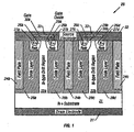
- Figure 1 is a cross-sectional side view of a vertical n-channel (i.e., NMOS) HVFET 20 in accordance with one embodiment of the present invention. It should be understood that the elements in the figures are representational, and are not drawn to scale in the interest of clarity. It is also appreciated that a p-channel transistor may be realized by utilizing the opposite conductivity types for all of the illustrated diffusion/doped regions. Furthermore, although the figure appears to show two separate devices, those of skill will understand that such transistor structures are commonly fabricated in an annular, interdigitated, or otherwise replicated manner.
- NMOS n-channel
- the device structure of Figure 1 includes an insulated-gate, field-effect transistor (IGFET) having a gate 30 (comprised, for example, of polysilicon), and a gate-insulating layer 29 that insulates gate 30 from the underlying semiconductor regions.
- Gate-insulating layer 29 may comprise ordinary silicon dioxide or another appropriate dielectric insulating material.
- the extended drain region of vertical HVFET 20 comprises two or more parallel N-type drift regions 22 situated between p-type body regions 26 and extending down to the N+ substrate 21.
- Figure 1 shows drift region 22a extending from beneath gate oxide 29a between P-body regions 26a & 26b down to N+ substrate 21.
- drift region 22b extends from gate oxide 29b between P-body regions 26c & 26d down to N+ substrate 21.
- Source electrode 32 is electrically connected to N+ source regions 27, which are disposed in respective P-body regions 26.
- N+ source region 27a is disposed in P-body region 26a;
- N+ region 27b is disposed in P-body region 27b, and so on.
- the area of the P-body regions directly beneath gate 30 (between N+ source regions 27 and drift regions 22) comprises the IGFET channel region of the transistor.
- the gate region is a metal-oxide semiconductor (MOS), and the IGFET is a NMOS transistor.
- MOS metal-oxide semiconductor
- the IGFET is a NMOS transistor.
- the channel regions of HVFET 20 are defined at one end by N+ source regions 27 and at the other end by N-type drift regions 22, which extend vertically from gate oxide 29 down to the N+ substrate 21. Insulating layers 33 separate gate 30 from source electrode 32.
- dielectric layers 28 extend vertically from beneath P-body regions 26 down to N+ substrate 21 along the full vertical length of the drift regions 22 thereby defining T-shaped semiconductor regions.
- dielectric layers 28 may comprise silicon dioxide, but other insulating materials, such as silicon nitride, may also be used.
- Field plate members 24 comprise a conducting layer of material such as heavily doped polysilicon, metal, metal alloys, etc.
- each of the field plate members 24 is electrically connected to source electrode 32.
- the field plate members may be connected to a separate electrode.
- Gates 30 are also connected to a separate electrode (not shown). Drain electrode 31 provides electrical connection to the bottom of N+ substrate 21.
- the extended drain region of vertical NMOS high-voltage transistor 20 of Figure 1 consists of a plurality of laterally interleaved layers of doped semiconductor material (e.g., n-type), insulating material (e.g., silicon dioxide), and conducting material (e.g., heavily-doped polysilicon).
- doped semiconductor material e.g., n-type
- insulating material e.g., silicon dioxide
- conducting material e.g., heavily-doped polysilicon
- the N-type drift region is normally very thick (i.e., long) and lightly doped; both of which contribute to high on state resistance.
- the doping in the N-type drift regions may be considerably higher, such that the on-state resistance is dramatically lowered. Lowering the on-state resistance is achieved in HVFET 20 by the use of multiple, parallel-arranged extended drain or drift regions.
- a high voltage e.g., 200V-1200V
- the doping profile in the drift regions 22 is tailored such that the resulting electric field is approximately constant along the path from the drain to the source.
- the doping concentration may be highest near the N+ substrate 21, lowest the near the P-body regions 26, and linearly graded in between.
- both the N-type drift regions 22 and oxide layers 28 should be designed so as to guard against prevent premature avalanche breakdown.
- Avalanche breakdown can be avoided by making the drift region relatively narrow, which reduces the ionization path and thereby increases the critical electric field at which avalanche occurs.
- making oxide layers 28 relatively wide allows the device structure to support a larger voltage for a given electric field.
- a device manufactured in accordance with Figure 1 having a drift region that is about 50 ⁇ m high and about 0.4 - 0.8 ⁇ m wide, with an oxide layer width in the approximate range of 3.0 - 4.0 ⁇ m is capable of supporting about 800V.
- the doping in the drift region may be linearly graded from about 5 x 10 15 cm -3 near the P-body regions to about 1 x 10 17 cm -3 near the N+ substrate.
- the on-state resistance of such a device is about 1.0 ohm-mm 2 .
- HVFET 20 may be improved when manufactured as a smaller total cell pitch (i.e., combined width of field plate, oxide layer and drift regions) because the contribution of each drift region is fairly constant.
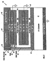
- HVFET 40 of Figure 2 operates according to the same principles discussed in connection with the transistor structure of Figure 1 , except that current flows laterally, as opposed to vertically, through the drift regions. Note that in the HVFET of Figure 2 , field plate members 44 are fully insulated from the semiconductor material by oxide layers 49.
- field plate member 44a is disposed within oxide layer 49a just below the source and drain electrodes 46 and 45, respectively.
- Field plate member 44b is disposed within oxide layer 49b below N-type drift region 42a and above N-type drift region 42b.
- the field plate members may be connected to a field plate electrode at a certain location out of the plane of the figure.
- the N-type drift region which comprises the extended drain of the transistor, extends laterally from beneath P-body region 48 across to N+ drain region 43.
- N+ drain region 43 connects both drift regions 42a & 42b with drain electrode 45.
- An N+ source region 47 which is electrically connected to source electrode 46, is disposed adjacent P-body region 48.
- the HVFET 40 utilizes a vertical MOS gate structure 12 that comprises a gate electrode 56 that connects to gate 55.
- gate 55 comprises a layer of polysilicon that extends vertically from gate electrode 56.
- Gate 55 extends below the P-body region, and may extend down to oxide layer 50, as shown.
- Gate 55 is insulated from N+ source region 47, P-body region 48, and N-type drift region 42 by gate oxide 53.
- An oxide region 58 separates gate electrode 56 from source electrode 46.
- Oxide layer 50 insulates N+ substrate 41 from gate 55, N-type drift region 42, and N+ drain region 43. As can be seen, oxide layer 50 extends laterally over N+ substrate 41 beneath each of the regions 42, 43, and 55. Substrate electrode 57 provides electrical connection to the bottom of N+ substrate 41. The substrate may serve as the bottom field plate for drift region 42b.
- HVFET 40 The on-state and off-state operations of HVFET 40 are similar to those described for the embodiment of Figure 1 .
- the source and drain electrodes are located on the top surface. This means that electrons flows down through N+ source region 47, across the channel region formed in P-body region 48 adjacent to gate oxide 53, laterally across the N-type drift regions 42, and up through the N+ drain region 43 before reaching the drain electrode.
- Figure 2 shows a trench gate structure
- planar gate structures could also be used.
- a trench drain structure could also be used in an alternative implementation.
- the HVFET of Figure 2 shows the extended drain region comprising two laterally extending, parallel N-type drift regions 42a and 42b, other HVFETs may utilize more than two parallel drift regions.
- the HVFET of Figure 2 is not limited to just two drift regions, but could include any number of layers of drift, oxide, and field plate regions within manufacturing limits.
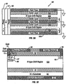
- Figures 3A & 3B illustrate another lateral HVFET not part of the present invention.
- Figure 3A is a top view of a lateral HVNMOS transistor 60
- Figure 3B is a cross-sectional side view of the same device, taken along cut lines A-A', which extends through drift region 62a.
- the source electrode 66, drain electrode 65, gate 75, gate oxide 73 and oxide layer 79 are not depicted in Figure 3A to avoid confusion. These elements are shown in the cross-sectional side view of Figure 3B .
- the lateral device structure of Figure 3 is similar to that shown in Figure 2 . But rather than orient the drift, oxide, and field plate layered regions on top of one another (vertically), the HVFET of Figure 3 has these regions oriented side-by-side. Unlike the HVFET of Figure 2 , each of the N-type drift regions 62, oxide layers 69, and field plate members 64 extend from underlying insulating layer 70 toward the upper substrate surface. Each of the N-type drift regions 62 and field plate members 64 are insulated from N+ substrate 61 by insulating layer 70. In one example, layer 70 comprises silicon dioxide. An additional electrode 77 provides electrical connection to the bottom of N+ substrate 61.
- HVNMOS transistor 60 The planar gate and drain configurations of HVNMOS transistor 60 are illustrated in the side view of Figure 3B .
- a trench drain structure and/or a trench gate structure may be utilized.
- a gate member 75 is disposed above P-body region 68 and is insulated from the semiconductor substrate by a gate oxide 73.
- Source electrode 66 contacts N+ source region 67, which is disposed in P-body region 68.
- P-body region 68 is itself shown disposed in N-type drift region 62.
- N+ drain region 63 is disposed at the opposite end of the N-type drift region 62 and is electrically connected to drain electrode 65.
- the HVFETs of Figures 2 and 3 show the field plate members being coupled to the lowest chip potential, e.g., ground.
- the source may be tied to the field plate members (at the lowest chip potential), or, alternatively, the source region may be left floating.
- the HVFETs of Figures 1-3 are not limited to a source follower configuration.
- Each of the transistor structures of the present invention may be implemented as a four-terminal device, wherein the drain, source, field plate members, and insulated gate members are connected to a separate circuit terminal. In another example, the field plate and insulated gate members may be connected together.
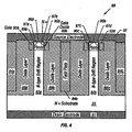
- transistor 80 comprises a plurality of parallel-arranged N-type drift regions 82 that extend vertically from P-body regions 86 down to the N+ substrate 81. Each of the drift regions 82 is adjoined on both sides by an oxide layer 88.
- N-type drift region 82a is bounded on one side by oxide layer 88a and on the opposite side by oxide layer 88b.
- a field plate member 84 Disposed within each of the oxide layers 88, and fully insulated from the drift region and substrate semiconductor materials, is a field plate member 84 that may be electrically connected to source electrode 92.
- the N-type drift regions 82, oxide layers 88, and field plate members 84 collectively comprise a parallel layered structure that extends in a lateral direction, which is perpendicular to the direction of current flow in the on-state.
- transistor 80 When transistor 80 is in the on-state, current flows vertically from the drain electrode 91 through the parallel N-type drift regions 82, through the MOS channel formed on the sidewalls of the P-body region, to the source electrode 92.
- the trench gate structure of vertical HVNMOS transistor 80 comprises gate members 90 disposed between field plate members 84 and P-body regions 86.
- a pair of N+ source regions 87 is disposed in each of P-body regions 86 on opposite sides.
- Each P-body region 86 is located at one end of a corresponding N-type drift region 82.
- a thin gate-insulating layer 89 e.g., oxide insulates each of gate members 90 (e.g., polysilicon) from the P-body semiconductor material.
- Figure 4 shows gate members 90a & 90b disposed along opposite sides of P-body region 86a.
- N+ source regions 87a & 87b are disposed in P-body region 86a at opposite sides adjacent to the gate members; both regions 87a & 87b are electrically connected to source electrode 92.
- P-body region 86a adjoins the source electrode at one end and drift region 82a at the other end.
- transistor 80 is in the on-state conducting channel regions are formed along the sides of P-body region 86a such that current flows from source electrode 92, through N+ regions 87, across P-body 86, down through N-type drift regions 82 and N+ substrate 81, to drain electrode 91.
- each P-body region 86 of Figure 4 may alternatively be replaced by a single N+ region that extends across the full width of region 86 adjacent to source electrode 92.
- the P-body region may be connected to the source electrode at various points (dimensionally into the page of the figure.)
- source electrode 92 may protrude through N+ source 87 to contact the underlying P-body region 86 (see Figure 5K ).
- the trench gate structure of the transistor of Figure 4 potentially offers an advantage of a simplified manufacturing process, due to the elimination of the T-shaped semiconductor regions shown in Figure 1 .
- the vertical HVNMOS structure of transistor 80 may provide lower on-resistance due to the elimination of the JFET structure formed between the P-body regions.
- Figures 5A-5K illustrate the various processing steps that may be employed to fabricate a vertical high-voltage transistor not part of the present invention.
- the described fabrication method may be used not only to form the device of Figure 5K , but also the vertical device structure shown in Figure 4 .
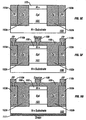
- Figure 5A shows a vertical high-voltage transistor after the initial processing step of forming an epitaxial layer 101 of n-type semiconductor material on an N+ substrate 100.
- the device structure should have an epitaxial layer that is about 15 ⁇ m to 120 ⁇ m thick.
- the epitaxial layer of the device shown in Figure 5 is 40 ⁇ m thick.
- the N+ substrate 100 is heavily doped to minimize its resistance to current flowing through to the drain electrode, which is located on the bottom of the substrate in the completed device.
- Substrate 100 may be thinned, for example, by grinding or etching, and metal may be deposited on its bottom surface to further reduce the on-resistance of the transistor. Most often, these processing steps would be performed after the topside processing has been completed.
- the thickness and doping of epitaxial layer 101 largely determine the Vbd of the device.
- the doping may be carried out as the epitaxial layer is being formed.
- the optimal doping profile is linearly graded from the drain (at the bottom, adjacent to N+ substrate 100) to the source (at the top). Tailoring the doping concentration so that it is heavier near the substrate 100 results in a more uniform electric-field distribution. Linear grading may stop at some point below the top surface of the epitaxial layer 101.
- the doping concentration is approximately 2 x 10 15 cm -3 near the P-body region to about 6 x 10 16 cm -3 near the N+ substrate 100.
- FIG. 5B shows a cross-sectional view of the device structure following etching of epitaxial layer 101 and part of substrate 100. Note that the lateral width of the etched trenches is determined by the combined thickness of the dielectric and conductive refill layers, as described below.
- the lateral thickness (i.e., width) of the N-type drift region(s) is desired to make the lateral thickness (i.e., width) of the N-type drift region(s) as narrow as can be reliably manufactured in order to achieve a very high Vbd with a low Rsp.
- a larger lateral thickness is easier to manufacture, but the specific on-resistance of the device suffers with a larger lateral thickness since the current is required to flow across a larger silicon area.
- the thickness is in the approximate range of 0.4 to 1.2 ⁇ m.
- the thickness of the mesa is about 1 ⁇ m.
- Figure 5C shows the device structure of Figure 5B after partial filling of the etched trenches with a dielectric material, e.g., silicon dioxide.
- a dielectric material e.g., silicon dioxide.
- oxide region 102a covers one side of etched epitaxial region 101, while oxide region 102b covers the other side of epitaxial region 101.
- Oxide region 102 also covers the top surface of N+ substrate 100 in each of the trenches.
- the dielectric material may be introduced into the trenches using a variety of well-known methods. For instance, regions 102 may be grown thermally, deposited by chemical vapor deposition, and/or spun on in liquid form. For a given lateral thickness of epitaxial layer material 101, the thickness of the dielectric layer may be set to provide a required breakdown voltage, with thicker dielectric layers providing a higher Vbd. However, thicker dielectric layers increase the cell pitch of the transistor structure and result in higher specific on-resistance. In one implementation, the device structure of Figure 5 has an oxide layer lateral thickness of 4 ⁇ m. For devices with other V bd performance, this thickness may be in the range of about 2 ⁇ m - 5 ⁇ m.
- Figure 5D illustrates the device structure of Figure 5C following the steps of filling the remaining portions of the trenches with a conductive material and planarizing the surface to form field plate regions 103.
- the conductive material may comprise a heavily doped polysilicon, a metal (or metal alloys), and/or silicide.
- Conductor regions 103a and 103b form the field plate members of the device.
- field plate members 103a and 103b should be made as narrow as can be reliably manufactured, since the field plate members occupy silicon area without directly contributing to device conductivity or breakdown voltage characteristics.
- the lateral thickness of field plate members 103 is approximately 0.5 ⁇ m - 1.0 ⁇ m.
- the planarization of the surface may be performed by conventional techniques such as chemical-mechanical polishing.
- fabrication of the extended drain region of the device is essentially complete.
- the remaining processing steps may be adapted to produce a stand-alone, high-voltage, depletion-mode MOSFET device structure (as shown in Figure 5G and Figure 6 ) or a high-voltage FET that incorporates a low-voltage MOSFET structure (e.g., Figure 5K ), or other high-voltage devices.
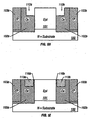
- Figure 5E is a cross-sectional side view of the device structure of Figure 5D after the introduction of an N+ source region 105 at the top surface of epitaxial layer 101.
- Source region 105 may be formed using ordinary deposition, diffusion, and/or implantation processing techniques.
- interlevel dielectric layer 106 After formation of the N+ source region 105 an interlevel dielectric layer 106 if formed over the device.
- interlevel dielectric layer 106 comprises ordinary silicon dioxide that may be deposited and patterned by conventional methods. Openings are formed in dielectric layer 106 and a conductive layer of material (e.g., metal, silicide, etc.) is deposited and patterned to produce the structure shown in Figure 5F .
- source electrode 109 provides electrical connection to N+ source region 105
- electrodes 110a and 110b provide electrical connection to field plate members 103a and 103b, respectively.
- FIG. 5G shows the device structure of Figure 5F following formation of a drain electrode 111 on the bottom of N+ substrate 100.
- drain electrode 111 may be formed using the conventional technique of metal sputtering.
- the bottom of the substrate may first be subjected to grinding, implanting, etc., to lower the drain contact resistance.
- the device of Figure 5G represents a completed high-voltage transistor having a stand-alone drift region; that is, the device of Figure 5G does not include a low-voltage, series MOSFET structure at the top of the epitaxial layer. Instead, the extended drift region formed by the epitaxial layer, itself, performs the function of the MOSFET without the inclusion of a P-body region. Practitioners in the arts will note that in this device structure current cannot be completely turned-off, since there exists a continuous n-type path for electrons to flow from source electrode 109 to drain electrode 111. Current flow in the device structure of Figure 5G , however, does saturate when the mesa-like epitaxial layer 101 is pinched-off at high drain voltages.
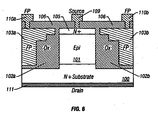
- the device structure of Figure 6 achieves pinch-off of the extended drain region at lower voltages than the device of Figure 5G . This is achieved by reducing the spacing between the field plate members 103 and epitaxial layer 101 near the top of the N-type drift region, thereby increasing the capacitance to pinch-off the vertical drift region at a relatively low voltage.
- Figure 6 shows a multi-tiered field plate structure extending laterally into oxide regions 102a & 102b to control the pinch-off voltage and, therefore, the saturation current.
- the field plate members may comprise a single step, a linearly graded lateral extension, or some other profile shape designed to achieve the same result.
- FIG. 5H-5K there is shown an alternative processing sequence that may be used to fabricate a vertical HVNMOS transistor that includes an insulated gate MOS structure.
- Trenches 112a and 112b are formed in respective dielectric layers 102a and 102b on opposite sides of epitaxial layer 101 to accommodate the formation of the insulated gate structure.
- the depth of trenches 112a and 112b extends from the surface of N+ source region 105 to a depth governed by the intended MOSFET channel length and field plating considerations. In this example, the trench depth is about 1-5 ⁇ m.
- trenches 112 may be formed by appropriate application of a patterned masking layer to the semiconductor substrate followed by conventional dry or wet etching techniques into oxide layer 102.
- Figure 5J shows the device after formation of gate dielectric layers 116 and gate members 113 within trenches 112.
- the gate dielectric layers 116a & 116b may be formed by growing or depositing oxide on the sidewalls of the stacked N+ source, P-body, and epitaxial regions.
- the device threshold voltage determines the thickness of layers 116.
- layers 116 comprise silicon dioxide having a thickness on the order of 25-100 nm (250 - 1000 angstroms).
- a portion of dielectric layers 112 isolates field plate members 103 from gate members 113.
- trenches 112 may expose the top portion of field plate 103 and the same processing steps used to create layers 116 may also be used to form dielectric layers on the sidewalls of the field plates to isolate the field plates from the gate members.
- a conductive material such as doped polysilicon, may be deposited to fill the remaining portions of the trenches.
- the doped polysilicon forms the gate members 113a and 113b of the MOS transistor structure.
- Figure 5J shows the device after introduction of a P-body region 107 and a N+ source region 105 at the top surface of epitaxial region 101. Regions 107 and 105 may be formed using standard implantation, deposition, and/or thermal diffusion processing steps. In the completed device, application of a sufficient voltage to gate members 113 causes a conductive channel to be formed along the sidewall portions of P-body region 107 between N+ source region 105 and epitaxial region 101.
- the channel length is therefore determined by the thickness of P-body region 107, which, for the particular example shown, may be approximately 0.5 ⁇ m - 3.0 ⁇ m, with the N+ source region 105 in the range of about 0.1-0.5 ⁇ m.
- a shorter channel length results in a lower channel resistance, which likewise reduces the on-resistance of the device. It should be understood, however, that a too short channel would cause punch-through problems.
- Figure 5K shows the completed HVFET device structure following formation of an interlevel dielectric layer 106 (e.g., silicon dioxide, silicon nitride, etc.).
- This layer may be deposited and patterned to form contact openings.
- the etching of layer 106 is followed by etching of the field plates, gate members, N+ and P-body regions.
- a conductive layer e.g., metal, silicide, etc.
- the optional etching step described above allows the source electrode to contact the P-body region without patterning the N+ source region, thus simplifying the process.
- a conductive layer may also be applied to the bottom of substrate 100 (after optional treatment by grinding, etching, implanting, etc.) to form the drain electrode 111.
- source electrode 109 is shown extending down to P-body 107 in the cross-sectional view of Figure 5K , in other examples electrode may only extend to the upper surface of source region 105. It should also be appreciated that electrode 109 does not separate region 105 into two separate source regions in the illustration of Figure 5K . Rather, electrode 109 is fabricated in the form of a plug that is surrounded by N+ material that comprises region 105.
- a high-voltage transistor with a low specific on-state resistance and that supports high voltage in the off-state includes one or more source regions disposed adjacent to a multi-layered extended drain structure which comprises extended drift regions separated from field plate members by one or more dielectric layers. With the field plate members at the lowest circuit potential, the transistor supports high voltages applied to the drain in the off-state.
Abstract
Description
- The present invention relates to semiconductor devices fabricated in a silicon substrate. More specifically, the present invention relates to field-effect semiconductor transistor structures capable of withstanding high voltages.
- High-voltage, field-effect transistors (HVFETs) are well known in the semiconductor arts. Most often, HVFETs comprise a device structure that includes an extended drain region that supports the applied high-voltage when the device is in the "off" state. HVFETs of this type are commonly used in power conversion applications such as AC/DC converters for offline power supplies, motor controls, and so on. These devices can be switched at high voltages and achieve a high blocking voltage in the off state while minimizing the resistance to current flow in the "on" state. The blocking or breakdown voltage is generally denoted as Vbd. The acronym Rsp refers to the product of the resistance and surface area, and is generally used to describe the on-state performance of the device. An example of a prior art HVFET having an extended drain region with a top layer of a conductivity type opposite that of the extended drain region is found in
U.S. Patent No. 4,811,075 . - In a conventional HVFET the extended drain region is usually lightly doped to support high voltages applied to the drain when the device is off. The length of the extended drain region is also increased to spread the electric field over a larger area so the device can sustain higher voltages. However, when the device is on (i.e., conducting) current flows through the extended drain region. The combined decrease in doping and increase length of the extended drain region therefore have the deleterious effect on the on-state performance of the device, as both cause an increase in on-state resistance. In other words, conventional high-voltage FET designs are characterized by a trade-off between Vbd and Rsp.
- To provide a quantitative example, a typical prior art vertical HVFET (NMOS-type) may have a Vbd of 600V with a Rsp of about 16 ohm-mm2. Increasing the length of the extended drain would affect device performance by increasing Vbd beyond 600V at the expense of a higher Rsp value. Conversely, reducing the length of the extended drain would improve the on-state resistance to a value below 16 ohm-mm2, but such a change in the device structure would also cause Vbd to be reduced to less than 600V.
- A device structure for supporting higher Vbd voltages with a low Rsp value is disclosed in
U.S. Patent Nos. 4,754,310 ,5,438,215 , and also in the article entitled, "Theory of Semiconductor Superjunction Devices" by T. Fujihira, Jpn. J. Appl. Phys., Vol. 36, pp. 6254-6262, Oct. 1977. In this device structure the extended drain region comprises alternating layers of semiconductor material having opposite conductivity types, e.g., PNPNP.... As high voltage is applied to the layers of one conductivity type, all of the layers are mutually depleted of charge carriers. This permits a high Vbd at much higher conducting layer doping concentrations as compared to single layer devices. The higher doping concentrations, of course, advantageously lower the Rsp of the transistor device. For example, in the article entitled, "A new generation of high voltage MOSFETs breaks the limit line of silicon" by G. Deboy et al., IEDM tech. Digest, pp. 683-685, 1998, the authors report a vertical NMOS device with a Vbd of 600V and a Rsp of about 4 ohm-mm2. - Another approach to the problem of achieving high-voltage capability is disclosed in the paper, "Realization of High Breakdown Voltage in Thin SOI Devices" by S. Merchant et al., Proc. Intl. Symp. on Power Devices and ICs, pp. 31-30 35, 1991. This paper teaches an extended drain region that comprises a thin layer of silicon situated on top of a buried oxide layer disposed on top of a semiconductor substrate. In operation, the underlying silicon substrate depletes charge from the thin silicon layer at high voltages. The authors claim that high values of Vbd are obtained as long as the top silicon layer is sufficiently thin and the buried oxide layer is sufficiently thick. For instance, a lateral NMOS device with Vbd of 600V and Rsp of about 8 ohm- mm2 is obtained using this approach.
- Other background references of possible interest to those skilled in the art include
U.S. Patent No. 6,184,555 ,6,191,447 ,6,075,259 ,5,998,833 ,5,637,898 , International Application No. PCT/IB98/02060 (International Publication No. WO 99/34449 -
Japanese Patent Publication No. 2001-085688A -
Japanese Patent Publication No. 2000-349288 - The document entitled "Oxide-bypassed VDMOS(OBVDMOS): an alternative to superjunction high voltage MOS power devices" by Liang, Y.C., et al. (Electron Device Letters, IEEE , vol.22, no.8, pp.407-409, Aug. 2001) proposes that the superjunction concept be used to overcome the ideal silicon MOSFET limit. A novel device structure termed oxide-bypassed VDMOS (OBVDMOS) that requires the well-established oxide thickness control instead of the difficult doping control in translating the limit to a higher blocking voltage is described.
-
International Patent Publication WO 97/35346 - Although the device structures described above achieve high Vbd with relatively low on-state resistance as compared to earlier designs, there is still an unsatisfied need for a high-voltage transistor structure that can support still high voltages while achieving a much lower on-state resistance.
- A vertical high-voltage transistor in accordance with the invention is set out in claim 1. Specific embodiments are defined in the dependent claims.
- The present invention is illustrated by way of example, and not limitation, in the figures of the accompanying drawings, wherein:
-
Figure 1 is a cross-sectional side view of a vertical high-voltage, field-effect transistor (HVFET) device structure in accordance with one embodiment of the present invention. -
Figure 2 is a cross-sectional side view of a lateral HVFET not part of the present invention. -
Figure 3A is a top view of lateral HVFET not part of of the present invention. -
Figure 3B is a cross-sectional side view of the lateral HVFET shown inFigure 3A , taken along cut lines A-A'. -
Figure 4 is a cross-sectional side view of a vertical HVFET device structure not part of the present invention. -
Figures 5A-5K are cross-sectional side views of a vertical HVFET device structure taken at various stages in a fabrication process not part of the present invention. -
Figure 6 is a cross-sectional side view of still another vertical HVFET device structure not part of the present invention. - Hight-voltage field-effect transistors having an extended drain or drift region and a method for making a high-voltage field-effect transistor are described. The HVFETs have a low specific on-state resistance and supports high voltage in the off-state. In the following description, numerous specific details are set forth, such as material types, doping levels, structural features, processing steps, etc., in order to provide a thorough understanding of the present invention. Practitioners having ordinary skill in the semiconductor arts will understand that the invention may be practiced without many of these details. In other instances, well-known elements, techniques, and processing steps have not been described in detail to avoid obscuring the invention.
-
Figure 1 is a cross-sectional side view of a vertical n-channel (i.e., NMOS) HVFET 20 in accordance with one embodiment of the present invention. It should be understood that the elements in the figures are representational, and are not drawn to scale in the interest of clarity. It is also appreciated that a p-channel transistor may be realized by utilizing the opposite conductivity types for all of the illustrated diffusion/doped regions. Furthermore, although the figure appears to show two separate devices, those of skill will understand that such transistor structures are commonly fabricated in an annular, interdigitated, or otherwise replicated manner. - The device structure of
Figure 1 includes an insulated-gate, field-effect transistor (IGFET) having a gate 30 (comprised, for example, of polysilicon), and a gate-insulating layer 29 that insulates gate 30 from the underlying semiconductor regions. Gate-insulating layer 29 may comprise ordinary silicon dioxide or another appropriate dielectric insulating material. The extended drain region ofvertical HVFET 20 comprises two or more parallel N-type drift regions 22 situated between p-type body regions 26 and extending down to theN+ substrate 21. For instance,Figure 1 shows driftregion 22a extending from beneathgate oxide 29a between P-body regions 26a & 26b down toN+ substrate 21. Similarly, driftregion 22b extends fromgate oxide 29b between P-body regions 26c & 26d down toN+ substrate 21. -
Source electrode 32 is electrically connected to N+ source regions 27, which are disposed in respective P-body regions 26. For example,N+ source region 27a is disposed in P-body region 26a;N+ region 27b is disposed in P-body region 27b, and so on. It is appreciated that a variety of alternative source electrode connections are also possible. The area of the P-body regions directly beneath gate 30 (between N+ source regions 27 and drift regions 22) comprises the IGFET channel region of the transistor. In this particular embodiment, the gate region is a metal-oxide semiconductor (MOS), and the IGFET is a NMOS transistor. Thus, the channel regions of HVFET 20 are defined at one end by N+ source regions 27 and at the other end by N-type drift regions 22, which extend vertically from gate oxide 29 down to theN+ substrate 21. Insulatinglayers 33 separate gate 30 fromsource electrode 32. - The n-type extended drain or drift regions 22 are separated laterally by insulating regions or dielectric layers 28. In the embodiment of
Figure 1 , dielectric layers 28 extend vertically from beneath P-body regions 26 down toN+ substrate 21 along the full vertical length of the drift regions 22 thereby defining T-shaped semiconductor regions. By way of example, dielectric layers 28 may comprise silicon dioxide, but other insulating materials, such as silicon nitride, may also be used. Disposed within each of the dielectric layers 28, and fully insulated from thesemiconductor substrate 21 and drift regions 22, is a field plate member 24. Field plate members 24 comprise a conducting layer of material such as heavily doped polysilicon, metal, metal alloys, etc. As shown in the embodiment ofFigure 1 , each of the field plate members 24 is electrically connected to sourceelectrode 32. Alternatively, the field plate members may be connected to a separate electrode. Gates 30 are also connected to a separate electrode (not shown).Drain electrode 31 provides electrical connection to the bottom ofN+ substrate 21. - The extended drain region of vertical NMOS high-
voltage transistor 20 ofFigure 1 consists of a plurality of laterally interleaved layers of doped semiconductor material (e.g., n-type), insulating material (e.g., silicon dioxide), and conducting material (e.g., heavily-doped polysilicon). In the on state, a sufficient voltage is applied to the gate such that a channel of electrons is formed along the surface of the P-body regions 26. This provides a path for electron current flow fromsource electrode 32, N+ source regions 27, through the channel regions formed in P-body regions 26, down through the N-type drift regions 22, through theN+ substrate 21, to drainelectrode 31. - Practitioners in the semiconductor arts will note that in a conventional vertical HVNMOS transistor, the N-type drift region is normally very thick (i.e., long) and lightly doped; both of which contribute to high on state resistance. In the device structure of
Figure 1 , on the other hand, the doping in the N-type drift regions may be considerably higher, such that the on-state resistance is dramatically lowered. Lowering the on-state resistance is achieved inHVFET 20 by the use of multiple, parallel-arranged extended drain or drift regions. - In the off state, a high voltage (e.g., 200V-1200V) is applied across the respective drain and
source electrodes N+ substrate 21, lowest the near the P-body regions 26, and linearly graded in between. - The thickness of both the N-type drift regions 22 and oxide layers 28 should be designed so as to guard against prevent premature avalanche breakdown. Avalanche breakdown can be avoided by making the drift region relatively narrow, which reduces the ionization path and thereby increases the critical electric field at which avalanche occurs. In the same regard, making oxide layers 28 relatively wide allows the device structure to support a larger voltage for a given electric field.
- By way of example, a device manufactured in accordance with
Figure 1 having a drift region that is about 50 µm high and about 0.4 - 0.8 µm wide, with an oxide layer width in the approximate range of 3.0 - 4.0 µm is capable of supporting about 800V. In such a device, the doping in the drift region may be linearly graded from about 5 x 1015 cm-3 near the P-body regions to about 1 x 1017 cm-3 near the N+ substrate. The on-state resistance of such a device is about 1.0 ohm-mm2. - Practitioners in the art will appreciate that the device performance for
HVFET 20 may be improved when manufactured as a smaller total cell pitch (i.e., combined width of field plate, oxide layer and drift regions) because the contribution of each drift region is fairly constant. - Referring now to
Figure 2 , there is shown a lateral NMOS high-voltage transistor 40 not part of the present invention.HVFET 40 ofFigure 2 operates according to the same principles discussed in connection with the transistor structure ofFigure 1 , except that current flows laterally, as opposed to vertically, through the drift regions. Note that in the HVFET ofFigure 2 , field plate members 44 are fully insulated from the semiconductor material by oxide layers 49. - In this example,
field plate member 44a is disposed withinoxide layer 49a just below the source and drainelectrodes Field plate member 44b is disposed withinoxide layer 49b below N-type drift region 42a and above N-type drift region 42b. The field plate members may be connected to a field plate electrode at a certain location out of the plane of the figure. The N-type drift region, which comprises the extended drain of the transistor, extends laterally from beneath P-body region 48 across toN+ drain region 43.N+ drain region 43 connects bothdrift regions 42a & 42b withdrain electrode 45. - An
N+ source region 47, which is electrically connected to sourceelectrode 46, is disposed adjacent P-body region 48. TheHVFET 40 utilizes a vertical MOS gate structure 12 that comprises agate electrode 56 that connects togate 55. In this example,gate 55 comprises a layer of polysilicon that extends vertically fromgate electrode 56.Gate 55 extends below the P-body region, and may extend down tooxide layer 50, as shown.Gate 55 is insulated fromN+ source region 47, P-body region 48, and N-type drift region 42 bygate oxide 53. Anoxide region 58 separatesgate electrode 56 fromsource electrode 46. -
Oxide layer 50 insulatesN+ substrate 41 fromgate 55, N-type drift region 42, andN+ drain region 43. As can be seen,oxide layer 50 extends laterally overN+ substrate 41 beneath each of theregions Substrate electrode 57 provides electrical connection to the bottom ofN+ substrate 41. The substrate may serve as the bottom field plate fordrift region 42b. - The on-state and off-state operations of HVFET 40 are similar to those described for the embodiment of
Figure 1 . In this case, however, the source and drain electrodes are located on the top surface. This means that electrons flows down throughN+ source region 47, across the channel region formed in P-body region 48 adjacent togate oxide 53, laterally across the N-type drift regions 42, and up through theN+ drain region 43 before reaching the drain electrode. - Note that even though
Figure 2 shows a trench gate structure, planar gate structures could also be used. Additionally, a trench drain structure could also be used in an alternative implementation. Furthermore, although the HVFET ofFigure 2 shows the extended drain region comprising two laterally extending, parallel N-type drift regions Figure 2 is not limited to just two drift regions, but could include any number of layers of drift, oxide, and field plate regions within manufacturing limits. -
Figures 3A & 3B illustrate another lateral HVFET not part of the present invention.Figure 3A is a top view of alateral HVNMOS transistor 60, andFigure 3B is a cross-sectional side view of the same device, taken along cut lines A-A', which extends throughdrift region 62a. (Note that thesource electrode 66,drain electrode 65,gate 75,gate oxide 73 andoxide layer 79 are not depicted inFigure 3A to avoid confusion. These elements are shown in the cross-sectional side view ofFigure 3B .) - The lateral device structure of
Figure 3 is similar to that shown inFigure 2 . But rather than orient the drift, oxide, and field plate layered regions on top of one another (vertically), the HVFET ofFigure 3 has these regions oriented side-by-side. Unlike the HVFET ofFigure 2 , each of the N-type drift regions 62, oxide layers 69, and field plate members 64 extend from underlying insulatinglayer 70 toward the upper substrate surface. Each of the N-type drift regions 62 and field plate members 64 are insulated fromN+ substrate 61 by insulatinglayer 70. In one example,layer 70 comprises silicon dioxide. Anadditional electrode 77 provides electrical connection to the bottom ofN+ substrate 61. - The planar gate and drain configurations of
HVNMOS transistor 60 are illustrated in the side view ofFigure 3B . Alternatively, a trench drain structure and/or a trench gate structure may be utilized. In this example, agate member 75 is disposed above P-body region 68 and is insulated from the semiconductor substrate by agate oxide 73.Source electrode 66 contactsN+ source region 67, which is disposed in P-body region 68. P-body region 68 is itself shown disposed in N-type drift region 62. -
N+ drain region 63 is disposed at the opposite end of the N-type drift region 62 and is electrically connected to drainelectrode 65. - The HVFETs of
Figures 2 and3 show the field plate members being coupled to the lowest chip potential, e.g., ground. The source may be tied to the field plate members (at the lowest chip potential), or, alternatively, the source region may be left floating. In other words, the HVFETs ofFigures 1-3 are not limited to a source follower configuration. Each of the transistor structures of the present invention may be implemented as a four-terminal device, wherein the drain, source, field plate members, and insulated gate members are connected to a separate circuit terminal. In another example, the field plate and insulated gate members may be connected together. - With reference now to
Figure 4 , there is shown a cross-sectional side view of anothervertical HVNMOS transistor 80 not part of the present invention. The device structure shown inFigure 4 is similar to that ofFigure 1 , except that the planar gate has been replaced by a trench gate structure. As in the vertical device structure ofFigure 1 ,transistor 80 comprises a plurality of parallel-arranged N-type drift regions 82 that extend vertically from P-body regions 86 down to the N+ substrate 81. Each of the drift regions 82 is adjoined on both sides by an oxide layer 88. For example, N-type drift region 82a is bounded on one side by oxide layer 88a and on the opposite side byoxide layer 88b. - Disposed within each of the oxide layers 88, and fully insulated from the drift region and substrate semiconductor materials, is a field plate member 84 that may be electrically connected to source
electrode 92. The N-type drift regions 82, oxide layers 88, and field plate members 84 collectively comprise a parallel layered structure that extends in a lateral direction, which is perpendicular to the direction of current flow in the on-state. Whentransistor 80 is in the on-state, current flows vertically from thedrain electrode 91 through the parallel N-type drift regions 82, through the MOS channel formed on the sidewalls of the P-body region, to thesource electrode 92. - The trench gate structure of
vertical HVNMOS transistor 80 comprises gate members 90 disposed between field plate members 84 and P-body regions 86. In the example ofFigure 4 , a pair of N+ source regions 87 is disposed in each of P-body regions 86 on opposite sides. Each P-body region 86 is located at one end of a corresponding N-type drift region 82. A thin gate-insulating layer 89 (e.g., oxide) insulates each of gate members 90 (e.g., polysilicon) from the P-body semiconductor material. - For example,
Figure 4 showsgate members 90a & 90b disposed along opposite sides of P-body region 86a.N+ source regions 87a & 87b are disposed in P-body region 86a at opposite sides adjacent to the gate members; bothregions 87a & 87b are electrically connected to sourceelectrode 92. P-body region 86a adjoins the source electrode at one end and driftregion 82a at the other end. Whentransistor 80 is in the on-state conducting channel regions are formed along the sides of P-body region 86a such that current flows fromsource electrode 92, through N+ regions 87, across P-body 86, down through N-type drift regions 82 and N+ substrate 81, to drainelectrode 91. - Practitioners in the art will appreciate that the pair of N+ source regions 87 shown disposed in each P-body region 86 of
Figure 4 may alternatively be replaced by a single N+ region that extends across the full width of region 86 adjacent to sourceelectrode 92. In this case, the P-body region may be connected to the source electrode at various points (dimensionally into the page of the figure.) In one example,source electrode 92 may protrude through N+ source 87 to contact the underlying P-body region 86 (seeFigure 5K ). - The trench gate structure of the transistor of
Figure 4 potentially offers an advantage of a simplified manufacturing process, due to the elimination of the T-shaped semiconductor regions shown inFigure 1 . Also, the vertical HVNMOS structure oftransistor 80 may provide lower on-resistance due to the elimination of the JFET structure formed between the P-body regions. -
Figures 5A-5K illustrate the various processing steps that may be employed to fabricate a vertical high-voltage transistor not part of the present invention. The described fabrication method may be used not only to form the device ofFigure 5K , but also the vertical device structure shown inFigure 4 . -
Figure 5A shows a vertical high-voltage transistor after the initial processing step of forming anepitaxial layer 101 of n-type semiconductor material on anN+ substrate 100. To support applied voltages in the range of 200V to 1000V the device structure should have an epitaxial layer that is about 15µm to 120µm thick. By way of example, the epitaxial layer of the device shown inFigure 5 is 40µm thick. TheN+ substrate 100 is heavily doped to minimize its resistance to current flowing through to the drain electrode, which is located on the bottom of the substrate in the completed device.Substrate 100 may be thinned, for example, by grinding or etching, and metal may be deposited on its bottom surface to further reduce the on-resistance of the transistor. Most often, these processing steps would be performed after the topside processing has been completed. - The thickness and doping of
epitaxial layer 101 largely determine the Vbd of the device. The doping may be carried out as the epitaxial layer is being formed. The optimal doping profile is linearly graded from the drain (at the bottom, adjacent to N+ substrate 100) to the source (at the top). Tailoring the doping concentration so that it is heavier near thesubstrate 100 results in a more uniform electric-field distribution. Linear grading may stop at some point below the top surface of theepitaxial layer 101. By way of example, for the example shown inFigure 5 the doping concentration is approximately 2 x 1015 cm-3 near the P-body region to about 6 x 1016 cm-3 near theN+ substrate 100. - After the
epitaxial layer 101 has been formed, the top surface oflayer 101 is appropriately masked and deep trenches are then etched into, or alternatively completely through, the epitaxial layer.Figure 5B shows a cross-sectional view of the device structure following etching ofepitaxial layer 101 and part ofsubstrate 100. Note that the lateral width of the etched trenches is determined by the combined thickness of the dielectric and conductive refill layers, as described below. - Spacing between adjacent trenches is determined by the required thickness of the remaining mesa of epitaxial layer material, which, in turn, is governed by the breakdown voltage requirements of the device. It is this mesa of epitaxial material that eventually forms the N-type drift region of the device structure. It should be understood that this mesa of material might extend a considerable lateral distance in an orthogonal direction (into the page). Although the example of
Figure 5 illustrates a device having an extended drain region that comprises a single N-type drift region, it is appreciated that the vertical high-voltage transistor ofFigure 5 may be constructed with a plurality of parallel-arranged N-type drift regions. Ideally, it is desired to make the lateral thickness (i.e., width) of the N-type drift region(s) as narrow as can be reliably manufactured in order to achieve a very high Vbd with a low Rsp. Of course, a larger lateral thickness is easier to manufacture, but the specific on-resistance of the device suffers with a larger lateral thickness since the current is required to flow across a larger silicon area. In one implementation, the thickness is in the approximate range of 0.4 to 1.2 µm. In this example, the thickness of the mesa is about 1µm. -
Figure 5C shows the device structure ofFigure 5B after partial filling of the etched trenches with a dielectric material, e.g., silicon dioxide. As shown, in the example ofFigure 5 oxide region 102a covers one side of etchedepitaxial region 101, whileoxide region 102b covers the other side ofepitaxial region 101. Oxide region 102 also covers the top surface ofN+ substrate 100 in each of the trenches. - The dielectric material may be introduced into the trenches using a variety of well-known methods. For instance, regions 102 may be grown thermally, deposited by chemical vapor deposition, and/or spun on in liquid form. For a given lateral thickness of
epitaxial layer material 101, the thickness of the dielectric layer may be set to provide a required breakdown voltage, with thicker dielectric layers providing a higher Vbd. However, thicker dielectric layers increase the cell pitch of the transistor structure and result in higher specific on-resistance. In one implementation, the device structure ofFigure 5 has an oxide layer lateral thickness of 4µm. For devices with other Vbd performance, this thickness may be in the range of about 2µm - 5µm. -
Figure 5D illustrates the device structure ofFigure 5C following the steps of filling the remaining portions of the trenches with a conductive material and planarizing the surface to form field plate regions 103. For example, the conductive material may comprise a heavily doped polysilicon, a metal (or metal alloys), and/or silicide.Conductor regions field plate members - At this point in the process, fabrication of the extended drain region of the device is essentially complete. The remaining processing steps may be adapted to produce a stand-alone, high-voltage, depletion-mode MOSFET device structure (as shown in
Figure 5G andFigure 6 ) or a high-voltage FET that incorporates a low-voltage MOSFET structure (e.g.,Figure 5K ), or other high-voltage devices. -
Figure 5E is a cross-sectional side view of the device structure ofFigure 5D after the introduction of anN+ source region 105 at the top surface ofepitaxial layer 101.Source region 105 may be formed using ordinary deposition, diffusion, and/or implantation processing techniques. - After formation of the
N+ source region 105 an interleveldielectric layer 106 if formed over the device. In the example ofFigure 5 , interleveldielectric layer 106 comprises ordinary silicon dioxide that may be deposited and patterned by conventional methods. Openings are formed indielectric layer 106 and a conductive layer of material (e.g., metal, silicide, etc.) is deposited and patterned to produce the structure shown inFigure 5F . In this cross-sectional view,source electrode 109 provides electrical connection toN+ source region 105, andelectrodes plate members -
Figure 5G shows the device structure ofFigure 5F following formation of adrain electrode 111 on the bottom ofN+ substrate 100. For example,drain electrode 111 may be formed using the conventional technique of metal sputtering. As described earlier, the bottom of the substrate may first be subjected to grinding, implanting, etc., to lower the drain contact resistance. - The device of
Figure 5G represents a completed high-voltage transistor having a stand-alone drift region; that is, the device ofFigure 5G does not include a low-voltage, series MOSFET structure at the top of the epitaxial layer. Instead, the extended drift region formed by the epitaxial layer, itself, performs the function of the MOSFET without the inclusion of a P-body region. Practitioners in the arts will note that in this device structure current cannot be completely turned-off, since there exists a continuous n-type path for electrons to flow fromsource electrode 109 to drainelectrode 111. Current flow in the device structure ofFigure 5G , however, does saturate when the mesa-like epitaxial layer 101 is pinched-off at high drain voltages. - The device structure of
Figure 6 achieves pinch-off of the extended drain region at lower voltages than the device ofFigure 5G . This is achieved by reducing the spacing between the field plate members 103 andepitaxial layer 101 near the top of the N-type drift region, thereby increasing the capacitance to pinch-off the vertical drift region at a relatively low voltage.Figure 6 shows a multi-tiered field plate structure extending laterally intooxide regions 102a & 102b to control the pinch-off voltage and, therefore, the saturation current. Alternatively, the field plate members may comprise a single step, a linearly graded lateral extension, or some other profile shape designed to achieve the same result. - Those skilled in the arts will appreciated that for certain circuit applications it may be advantageous to utilize the stand-alone transistor structure of
Figure 5G (orFigure 6 ) in series with an ordinary external, low-voltage switching MOSFET. In such an application the low-voltage (e.g., 40V) MOSFET could be used for switching purposes in order to completely turn off current flow in the high-voltage (e.g., 700V) transistor device. - Referring now to
Figures 5H-5K , there is shown an alternative processing sequence that may be used to fabricate a vertical HVNMOS transistor that includes an insulated gate MOS structure. -
Trenches dielectric layers epitaxial layer 101 to accommodate the formation of the insulated gate structure. The depth oftrenches N+ source region 105 to a depth governed by the intended MOSFET channel length and field plating considerations. In this example, the trench depth is about 1-5µm. By way of example, trenches 112 may be formed by appropriate application of a patterned masking layer to the semiconductor substrate followed by conventional dry or wet etching techniques into oxide layer 102. -
Figure 5J shows the device after formation of gatedielectric layers 116 and gate members 113 within trenches 112. The gatedielectric layers 116a & 116b may be formed by growing or depositing oxide on the sidewalls of the stacked N+ source, P-body, and epitaxial regions. The device threshold voltage determines the thickness oflayers 116. In one example, layers 116 comprise silicon dioxide having a thickness on the order of 25-100 nm (250 - 1000 angstroms). - In the example shown, a portion of dielectric layers 112 isolates field plate members 103 from gate members 113. Alternatively, trenches 112 may expose the top portion of field plate 103 and the same processing steps used to create
layers 116 may also be used to form dielectric layers on the sidewalls of the field plates to isolate the field plates from the gate members. - Once
dielectric layers 116 have been formed on the sidewalls of trenches 112, a conductive material, such as doped polysilicon, may be deposited to fill the remaining portions of the trenches. In this implementation, the doped polysilicon forms thegate members Figure 5J shows the device after introduction of a P-body region 107 and aN+ source region 105 at the top surface ofepitaxial region 101.Regions body region 107 betweenN+ source region 105 andepitaxial region 101. The channel length is therefore determined by the thickness of P-body region 107, which, for the particular example shown, may be approximately 0.5µm - 3.0µm, with theN+ source region 105 in the range of about 0.1-0.5µm. A shorter channel length results in a lower channel resistance, which likewise reduces the on-resistance of the device. It should be understood, however, that a too short channel would cause punch-through problems. -
Figure 5K shows the completed HVFET device structure following formation of an interlevel dielectric layer 106 (e.g., silicon dioxide, silicon nitride, etc.). This layer may be deposited and patterned to form contact openings. In the embodiment shown, the etching oflayer 106 is followed by etching of the field plates, gate members, N+ and P-body regions. This is followed by deposition and patterning of a conductive layer (e.g., metal, silicide, etc.) to createsource electrode 109, gate electrodes 115, and field plate electrodes 110, which provide electrical connection to the respective regions of the device. The optional etching step described above allows the source electrode to contact the P-body region without patterning the N+ source region, thus simplifying the process. A conductive layer may also be applied to the bottom of substrate 100 (after optional treatment by grinding, etching, implanting, etc.) to form thedrain electrode 111. - Note that while
source electrode 109 is shown extending down to P-body 107 in the cross-sectional view ofFigure 5K , in other examples electrode may only extend to the upper surface ofsource region 105. It should also be appreciated thatelectrode 109 does not separateregion 105 into two separate source regions in the illustration ofFigure 5K . Rather,electrode 109 is fabricated in the form of a plug that is surrounded by N+ material that comprisesregion 105. - Thus there is provided a high-voltage transistor with a low specific on-state resistance and that supports high voltage in the off-state includes one or more source regions disposed adjacent to a multi-layered extended drain structure which comprises extended drift regions separated from field plate members by one or more dielectric layers. With the field plate members at the lowest circuit potential, the transistor supports high voltages applied to the drain in the off-state.
Claims (8)
- A vertical high-voltage transistor (20) comprising:a drain region of a first conductivity type comprising a heavily doped substrate (21) of said first conductivity type;a plurality of body regions (26) of a second conductivity type opposite to the first conductivity type:characterized in that the dielectric layers (28) extend vertically from beneath respective body regions (26) down to the substrate (21) along a full vertical length of the drift regions (22) thereby defining T-shaped semiconductor regions, each underlying a respective gate insulating layer (29).a plurality of parallel drift regions (22) of the first conductivity type, each of the drift regions (22) extending in a first direction from the drain region to one or more of the body regions (26);field plate members (24) that extend in the first direction, each of the field plate members (24) being spaced-apart in a second direction and insulated from the drift regions (22) by a dielectric layer (28);a plurality of source regions (27) of the first conductivity type, each of the source regions (27) adjoining one of the body regions (26); insulated gate members (30) respectively disposed above each body region (26) and each drift region (22) and separated from said body and drift regions by a gate in gate insulating layer (29); thereby defining channel regions, each comprised in an area of a respective body region (26) directly beneath an insulated gate member (30) and extending in the second direction from a respective one of the source regions (27) to one of the drift regions (22), the drift regions (22) each extending from beneath a respective gate insulating layer (29) between two body regions (26) down to the substrate (21),
- The vertical high-voltagc transistor according to claim 1 further comprising:a drain electrode electrically connected to the drain region; anda source electrode electrically connected to the source regions (27).
- The vertical high-voltage transistor according to claim 1 wherein the drift regions (22) have a length oriented in the first direction and a width oriented in the second direction, the length being more than five times the width.
- The vertical high-voltage transistor according to claim 1 wherein the substrate (21) has a substantially planar bottom surface, the first direction is a vertical direction perpendicular to the bottom surface of the substrate (21), and the second direction is a lateral direction parallel to the bottom surface of the substrate (21).
- The vertical high-voltage transistor according to claim 1 wherein the dielectric layers (28) comprise silicon dioxide.
- A vertical high-voltage transistor according to claim 1 wherein the drift regions (22) have a doping that is higher near the drain region and lower near the body regions (26).
- The vertical high-voltage transistor according to claim 1 wherein the drift regions (22) have a linearly graded doping profile.
- The vertical high-voltage transistor according to claim 1 wherein the doping profile in the drift regions (22) is tailored such that the resulting electric field is approximately constant along the path from the drain region to the source regions.
Applications Claiming Priority (3)
| Application Number | Priority Date | Filing Date | Title |
|---|---|---|---|
| US09/948,930 US6573558B2 (en) | 2001-09-07 | 2001-09-07 | High-voltage vertical transistor with a multi-layered extended drain structure |
| US948930 | 2001-09-07 | ||
| EP02255726A EP1291926A3 (en) | 2001-09-07 | 2002-08-16 | High-voltage semiconductor devices |
Related Parent Applications (2)
| Application Number | Title | Priority Date | Filing Date |
|---|---|---|---|
| EP02255726A Division EP1291926A3 (en) | 2001-09-07 | 2002-08-16 | High-voltage semiconductor devices |
| EP02255726.8 Division | 2002-08-16 |
Publications (3)
| Publication Number | Publication Date |
|---|---|
| EP1528600A2 EP1528600A2 (en) | 2005-05-04 |
| EP1528600A3 EP1528600A3 (en) | 2008-08-06 |
| EP1528600B1 true EP1528600B1 (en) | 2012-03-28 |
Family
ID=25488403
Family Applications (3)
| Application Number | Title | Priority Date | Filing Date |
|---|---|---|---|
| EP04078400A Expired - Lifetime EP1528600B1 (en) | 2001-09-07 | 2002-08-16 | Vertical high-voltage transistor |
| EP10184129A Withdrawn EP2264778A3 (en) | 2001-09-07 | 2002-08-16 | High-voltage vertical insulated gate transistor |
| EP02255726A Withdrawn EP1291926A3 (en) | 2001-09-07 | 2002-08-16 | High-voltage semiconductor devices |
Family Applications After (2)
| Application Number | Title | Priority Date | Filing Date |
|---|---|---|---|
| EP10184129A Withdrawn EP2264778A3 (en) | 2001-09-07 | 2002-08-16 | High-voltage vertical insulated gate transistor |
| EP02255726A Withdrawn EP1291926A3 (en) | 2001-09-07 | 2002-08-16 | High-voltage semiconductor devices |
Country Status (4)
| Country | Link |
|---|---|
| US (7) | US6573558B2 (en) |
| EP (3) | EP1528600B1 (en) |
| JP (3) | JP4436598B2 (en) |
| AT (1) | ATE551725T1 (en) |
Families Citing this family (118)
| Publication number | Priority date | Publication date | Assignee | Title |
|---|---|---|---|---|
| US6573550B2 (en) * | 2000-01-28 | 2003-06-03 | General Electronics Applications, Inc. | Semiconductor with high-voltage components and low-voltage components on a shared die |
| US6853033B2 (en) * | 2001-06-05 | 2005-02-08 | National University Of Singapore | Power MOSFET having enhanced breakdown voltage |
| US6555873B2 (en) * | 2001-09-07 | 2003-04-29 | Power Integrations, Inc. | High-voltage lateral transistor with a multi-layered extended drain structure |
| US6635544B2 (en) * | 2001-09-07 | 2003-10-21 | Power Intergrations, Inc. | Method of fabricating a high-voltage transistor with a multi-layered extended drain structure |
| US7221011B2 (en) * | 2001-09-07 | 2007-05-22 | Power Integrations, Inc. | High-voltage vertical transistor with a multi-gradient drain doping profile |
| US6573558B2 (en) * | 2001-09-07 | 2003-06-03 | Power Integrations, Inc. | High-voltage vertical transistor with a multi-layered extended drain structure |
| US7786533B2 (en) * | 2001-09-07 | 2010-08-31 | Power Integrations, Inc. | High-voltage vertical transistor with edge termination structure |
| US6747312B2 (en) | 2002-05-01 | 2004-06-08 | International Rectifier Corporation | Rad hard MOSFET with graded body diode junction and reduced on resistance |
| KR20060013397A (en) | 2003-05-13 | 2006-02-09 | 코닌클리즈케 필립스 일렉트로닉스 엔.브이. | Semiconductor device with a field shaping region |
| US7638841B2 (en) | 2003-05-20 | 2009-12-29 | Fairchild Semiconductor Corporation | Power semiconductor devices and methods of manufacture |
| GB0314390D0 (en) * | 2003-06-20 | 2003-07-23 | Koninkl Philips Electronics Nv | Trench field effect transistor structure |
| TWI243399B (en) * | 2003-09-24 | 2005-11-11 | Sanken Electric Co Ltd | Nitride semiconductor device |
| TWI240439B (en) * | 2003-09-24 | 2005-09-21 | Sanken Electric Co Ltd | Nitride semiconductor device and manufacturing method thereof |
| GB0327792D0 (en) * | 2003-11-29 | 2003-12-31 | Koninkl Philips Electronics Nv | Trench insulated gate field effect transistor |
| US7683454B2 (en) * | 2003-12-05 | 2010-03-23 | Stmicroelectronics S.A. | MOS power component with a reduced surface area |
| US20050121691A1 (en) * | 2003-12-05 | 2005-06-09 | Jean-Luc Morand | Active semiconductor component with a reduced surface area |
| CN103199017B (en) * | 2003-12-30 | 2016-08-03 | 飞兆半导体公司 | Form buried conductive layer method, material thickness control methods, form transistor method |
| DE102004007197B4 (en) * | 2004-02-13 | 2012-11-08 | Infineon Technologies Ag | High-pass semiconductor device with low forward voltage |
| CN100576564C (en) * | 2004-03-15 | 2009-12-30 | Nxp股份有限公司 | The metal-oxide-semiconductor high-voltage device structure of tapered unit cell |
| US7482654B2 (en) * | 2004-04-20 | 2009-01-27 | International Rectifier Corporation | MOSgated power semiconductor device with source field electrode |
| DE102004024344B4 (en) * | 2004-05-17 | 2010-04-15 | Infineon Technologies Ag | Method of manufacturing a power semiconductor device and power semiconductor device |
| US7268395B2 (en) * | 2004-06-04 | 2007-09-11 | International Rectifier Corporation | Deep trench super switch device |
| JP4959928B2 (en) * | 2004-09-07 | 2012-06-27 | 株式会社東芝 | Insulated gate semiconductor device |
| DE102004044619B4 (en) * | 2004-09-13 | 2009-07-16 | Infineon Technologies Ag | Capacitor structure in trench structures of semiconductor devices and semiconductor devices with such capacitor structures and method for making the same |
| DE102004046697B4 (en) * | 2004-09-24 | 2020-06-10 | Infineon Technologies Ag | High-voltage-resistant semiconductor component with vertically conductive semiconductor body regions and a trench structure, and method for producing the same |
| DE102004054352B3 (en) * | 2004-11-09 | 2006-02-16 | Infineon Technologies Ag | Capacitor structure in semiconductor component trough structures, comprises conducting islands made of metallic and/or semiconducting materials and/or metal compounds |
| JP4974454B2 (en) * | 2004-11-15 | 2012-07-11 | 株式会社豊田中央研究所 | Semiconductor device |
| WO2006085267A2 (en) * | 2005-02-08 | 2006-08-17 | Nxp B.V. | Semiconductor device with trench field plate |
| DE102005011967B4 (en) * | 2005-03-14 | 2007-07-19 | Infineon Technologies Ag | Semiconductor device with drift path and trench structure and method for producing the same |
| JP2006303287A (en) * | 2005-04-22 | 2006-11-02 | Toshiba Corp | Power semiconductor apparatus |
| JP2007019289A (en) * | 2005-07-08 | 2007-01-25 | Sanken Electric Co Ltd | Semiconductor device |
| TWI251922B (en) * | 2005-07-14 | 2006-03-21 | Siliconware Precision Industries Co Ltd | Multichip stack structure |
| DE102005035699B4 (en) * | 2005-07-27 | 2010-09-16 | Infineon Technologies Austria Ag | Semiconductor power device with charge compensation structure and method of making the same |
| DE102005048447B4 (en) * | 2005-10-07 | 2007-07-19 | Infineon Technologies Ag | Semiconductor power device with charge compensation structure and method of making the same |
| US7554153B2 (en) * | 2006-03-07 | 2009-06-30 | International Rectifier Corporation | Power semiconductor device |
| US7521773B2 (en) * | 2006-03-31 | 2009-04-21 | Fairchild Semiconductor Corporation | Power device with improved edge termination |
| US8093621B2 (en) | 2008-12-23 | 2012-01-10 | Power Integrations, Inc. | VTS insulated gate bipolar transistor |
| US8653583B2 (en) * | 2007-02-16 | 2014-02-18 | Power Integrations, Inc. | Sensing FET integrated with a high-voltage transistor |
| US7468536B2 (en) | 2007-02-16 | 2008-12-23 | Power Integrations, Inc. | Gate metal routing for transistor with checkerboarded layout |
| US7557406B2 (en) * | 2007-02-16 | 2009-07-07 | Power Integrations, Inc. | Segmented pillar layout for a high-voltage vertical transistor |
| US7595523B2 (en) | 2007-02-16 | 2009-09-29 | Power Integrations, Inc. | Gate pullback at ends of high-voltage vertical transistor structure |
| US7859037B2 (en) * | 2007-02-16 | 2010-12-28 | Power Integrations, Inc. | Checkerboarded high-voltage vertical transistor layout |
| CN101868856B (en) | 2007-09-21 | 2014-03-12 | 飞兆半导体公司 | Superjunction structures for power devices and methods of manufacture |
| US7875962B2 (en) * | 2007-10-15 | 2011-01-25 | Power Integrations, Inc. | Package for a power semiconductor device |
| US7911023B2 (en) * | 2007-11-06 | 2011-03-22 | Denso Corporation | Semiconductor apparatus including a double-sided electrode element and method for manufacturing the same |
| US9480254B2 (en) * | 2008-05-08 | 2016-11-01 | Aquatrols Corporation Of America | Systemic mitigation of environmental stress on plants and the fruit thereof |
| GB2460471B (en) * | 2008-05-31 | 2011-11-23 | Filtronic Compound Semiconductors Ltd | A field effect transistor and a method of manufacture thereof |
| US7964912B2 (en) | 2008-09-18 | 2011-06-21 | Power Integrations, Inc. | High-voltage vertical transistor with a varied width silicon pillar |
| US8174067B2 (en) * | 2008-12-08 | 2012-05-08 | Fairchild Semiconductor Corporation | Trench-based power semiconductor devices with increased breakdown voltage characteristics |
| US8304829B2 (en) * | 2008-12-08 | 2012-11-06 | Fairchild Semiconductor Corporation | Trench-based power semiconductor devices with increased breakdown voltage characteristics |
| US7871882B2 (en) * | 2008-12-20 | 2011-01-18 | Power Integrations, Inc. | Method of fabricating a deep trench insulated gate bipolar transistor |
| US20100155831A1 (en) * | 2008-12-20 | 2010-06-24 | Power Integrations, Inc. | Deep trench insulated gate bipolar transistor |
| US8227855B2 (en) * | 2009-02-09 | 2012-07-24 | Fairchild Semiconductor Corporation | Semiconductor devices with stable and controlled avalanche characteristics and methods of fabricating the same |
| JP2010186760A (en) * | 2009-02-10 | 2010-08-26 | Panasonic Corp | Semiconductor device and method of manufacturing the same |
| US8148749B2 (en) * | 2009-02-19 | 2012-04-03 | Fairchild Semiconductor Corporation | Trench-shielded semiconductor device |
| US8049276B2 (en) | 2009-06-12 | 2011-11-01 | Fairchild Semiconductor Corporation | Reduced process sensitivity of electrode-semiconductor rectifiers |
| US8207455B2 (en) * | 2009-07-31 | 2012-06-26 | Power Integrations, Inc. | Power semiconductor package with bottom surface protrusions |
| US8115457B2 (en) | 2009-07-31 | 2012-02-14 | Power Integrations, Inc. | Method and apparatus for implementing a power converter input terminal voltage discharge circuit |
| US8207577B2 (en) * | 2009-09-29 | 2012-06-26 | Power Integrations, Inc. | High-voltage transistor structure with reduced gate capacitance |
| US7893754B1 (en) | 2009-10-02 | 2011-02-22 | Power Integrations, Inc. | Temperature independent reference circuit |
| US8634218B2 (en) * | 2009-10-06 | 2014-01-21 | Power Integrations, Inc. | Monolithic AC/DC converter for generating DC supply voltage |
| US8310845B2 (en) * | 2010-02-10 | 2012-11-13 | Power Integrations, Inc. | Power supply circuit with a control terminal for different functional modes of operation |
| US8432000B2 (en) | 2010-06-18 | 2013-04-30 | Fairchild Semiconductor Corporation | Trench MOS barrier schottky rectifier with a planar surface using CMP techniques |
| US8252648B2 (en) * | 2010-06-29 | 2012-08-28 | Alpha & Omega Semiconductor, Inc. | Power MOSFET device with self-aligned integrated Schottky and its manufacturing method |
| JP2012099601A (en) * | 2010-11-01 | 2012-05-24 | Sumitomo Electric Ind Ltd | Semiconductor device and method of manufacturing the same |
| US8357579B2 (en) * | 2010-11-30 | 2013-01-22 | Taiwan Semiconductor Manufacturing Company, Ltd. | Methods of forming integrated circuits |
| CN102184944B (en) * | 2011-04-29 | 2013-01-02 | 南京邮电大学 | Junction terminal structure of lateral power device |
| US8742490B2 (en) * | 2011-05-02 | 2014-06-03 | Monolithic Power Systems, Inc. | Vertical power transistor die packages and associated methods of manufacturing |
| US9054133B2 (en) | 2011-09-21 | 2015-06-09 | Globalfoundries Singapore Pte. Ltd. | High voltage trench transistor |
| US8492226B2 (en) * | 2011-09-21 | 2013-07-23 | Globalfoundries Singapore Pte. Ltd. | Trench transistor |
| CN102332396A (en) * | 2011-10-27 | 2012-01-25 | 博嘉圣(福州)微电子科技有限公司 | Method for designing power vertical double-diffused metal-oxide-semiconductor field effect transistor (VDMOSFET) structure |
| US9443972B2 (en) | 2011-11-30 | 2016-09-13 | Infineon Technologies Austria Ag | Semiconductor device with field electrode |
| US8614482B2 (en) * | 2011-12-30 | 2013-12-24 | Force Mos Technology Co., Ltd. | Semiconductor power device having improved termination structure for mask saving |
| US8587054B2 (en) | 2011-12-30 | 2013-11-19 | Force Mos Technology Co., Ltd. | Trench MOSFET with resurf stepped oxide and diffused drift region |
| US8854065B2 (en) | 2012-01-13 | 2014-10-07 | Infineon Technologies Austria Ag | Current measurement in a power transistor |
| US8704296B2 (en) * | 2012-02-29 | 2014-04-22 | Fairchild Semiconductor Corporation | Trench junction field-effect transistor |
| US8946814B2 (en) * | 2012-04-05 | 2015-02-03 | Icemos Technology Ltd. | Superjunction devices having narrow surface layout of terminal structures, buried contact regions and trench gates |
| US9054065B2 (en) | 2012-04-30 | 2015-06-09 | Skyworks Solutions, Inc. | Bipolar transistor having collector with grading |
| US8653600B2 (en) | 2012-06-01 | 2014-02-18 | Power Integrations, Inc. | High-voltage monolithic schottky device structure |
| KR101680511B1 (en) | 2012-06-14 | 2016-11-28 | 스카이워크스 솔루션즈, 인코포레이티드 | Power amplifier modules including bipolar transistor with grading and related systems, devices, and methods |
| JP5802636B2 (en) * | 2012-09-18 | 2015-10-28 | 株式会社東芝 | Semiconductor device and manufacturing method thereof |
| US9437440B2 (en) | 2012-11-21 | 2016-09-06 | Infineon Technologies Dresden Gmbh | Method for manufacturing a semiconductor device |
| US9136379B2 (en) * | 2013-04-26 | 2015-09-15 | Alpha & Omega Semiconductor, Inc. | Bottom source substrateless power MOSFET |
| TWI572040B (en) * | 2013-06-21 | 2017-02-21 | 竹懋科技股份有限公司 | Structure of trench-vertical double diffused mos transistor and method of forming the same |
| US9455621B2 (en) | 2013-08-28 | 2016-09-27 | Power Integrations, Inc. | Controller IC with zero-crossing detector and capacitor discharge switching element |
| KR20150030799A (en) * | 2013-09-12 | 2015-03-23 | 매그나칩 반도체 유한회사 | Semiconductor Device and Fabricating Method Thereof |
| US9224854B2 (en) * | 2013-10-03 | 2015-12-29 | Texas Instruments Incorporated | Trench gate trench field plate vertical MOSFET |
| US10325988B2 (en) | 2013-12-13 | 2019-06-18 | Power Integrations, Inc. | Vertical transistor device structure with cylindrically-shaped field plates |
| US9543396B2 (en) | 2013-12-13 | 2017-01-10 | Power Integrations, Inc. | Vertical transistor device structure with cylindrically-shaped regions |
| US9324784B2 (en) * | 2014-04-10 | 2016-04-26 | Semiconductor Components Industries, Llc | Electronic device having a termination region including an insulating region |
| US9343528B2 (en) | 2014-04-10 | 2016-05-17 | Semiconductor Components Industries, Llc | Process of forming an electronic device having a termination region including an insulating region |
| US9349795B2 (en) * | 2014-06-20 | 2016-05-24 | Infineon Technologies Austria Ag | Semiconductor switching device with different local threshold voltage |
| US9293533B2 (en) | 2014-06-20 | 2016-03-22 | Infineon Technologies Austria Ag | Semiconductor switching devices with different local transconductance |
| US9231049B1 (en) * | 2014-06-20 | 2016-01-05 | Infineon Technologies Austria Ag | Semiconductor switching device with different local cell geometry |
| US9324823B2 (en) | 2014-08-15 | 2016-04-26 | Infineon Technologies Austria Ag | Semiconductor device having a tapered gate structure and method |
| DE102014112379A1 (en) * | 2014-08-28 | 2016-03-03 | Infineon Technologies Austria Ag | A semiconductor device having a termination mesa between a termination structure and a cell array of field electrode structures |
| JP6203697B2 (en) | 2014-09-30 | 2017-09-27 | 株式会社東芝 | Semiconductor device and manufacturing method thereof |
| JP6299581B2 (en) | 2014-12-17 | 2018-03-28 | 三菱電機株式会社 | Semiconductor device |
| US9583482B2 (en) | 2015-02-11 | 2017-02-28 | Monolith Semiconductor Inc. | High voltage semiconductor devices and methods of making the devices |
| US9478639B2 (en) | 2015-02-27 | 2016-10-25 | Infineon Technologies Austria Ag | Electrode-aligned selective epitaxy method for vertical power devices |
| US10492834B2 (en) * | 2015-03-11 | 2019-12-03 | Warsaw Orthopedic, Inc. | Surgical instrument system and method |
| DE102015108091A1 (en) * | 2015-05-21 | 2016-11-24 | Infineon Technologies Dresden Gmbh | Transistor arrangement with power transistors and voltage-limiting components |
| DE102015111210A1 (en) * | 2015-07-10 | 2017-01-12 | Infineon Technologies Dresden Gmbh | METHOD FOR FILLING A DIG AND SEMICONDUCTOR ELEMENT |
| JP6400545B2 (en) | 2015-09-11 | 2018-10-03 | 株式会社東芝 | Semiconductor device |
| US9667154B2 (en) | 2015-09-18 | 2017-05-30 | Power Integrations, Inc. | Demand-controlled, low standby power linear shunt regulator |
| US9973183B2 (en) | 2015-09-28 | 2018-05-15 | Power Integrations, Inc. | Field-effect transistor device with partial finger current sensing FETs |
| US9602009B1 (en) | 2015-12-08 | 2017-03-21 | Power Integrations, Inc. | Low voltage, closed loop controlled energy storage circuit |
| US9629218B1 (en) | 2015-12-28 | 2017-04-18 | Power Integrations, Inc. | Thermal protection for LED bleeder in fault condition |
| US9983239B2 (en) | 2016-05-13 | 2018-05-29 | Power Integrations, Inc. | Integrated linear current sense circuitry for semiconductor transistor devices |
| WO2018030990A1 (en) | 2016-08-08 | 2018-02-15 | Power Integrations, Inc. | Integrated circuit fast temperature sensing of a semiconductor switching device |
| CN107768436A (en) * | 2017-10-20 | 2018-03-06 | 电子科技大学 | A kind of trench gate electric charge memory type IGBT and its manufacture method |
| CN107768434A (en) * | 2017-10-20 | 2018-03-06 | 电子科技大学 | A kind of two-way IGBT and its manufacture method |
| CN107681006A (en) * | 2017-11-01 | 2018-02-09 | 苏州凤凰芯电子科技有限公司 | A kind of shield grid MOS structure with stairstepping oxide layer |
| US10971624B2 (en) * | 2018-03-19 | 2021-04-06 | Macronix International Co., Ltd. | High-voltage transistor devices with two-step field plate structures |
| CN110676321A (en) * | 2018-07-03 | 2020-01-10 | 无锡华润华晶微电子有限公司 | Trench MOSFET and method of manufacturing the same |
| CN114503279A (en) * | 2019-08-12 | 2022-05-13 | 麦斯功率半导体股份有限公司 | High density power device with selectively shielded recessed field effect plate |
| US11316042B2 (en) * | 2020-01-31 | 2022-04-26 | Power Integrations, Inc. | Process and structure for a superjunction device |
| TWI802305B (en) * | 2022-03-03 | 2023-05-11 | 力晶積成電子製造股份有限公司 | Semiconductor structure and method for manufacturing buried field plates |
Family Cites Families (140)
| Publication number | Priority date | Publication date | Assignee | Title |
|---|---|---|---|---|
| JPS5638867A (en) | 1979-09-07 | 1981-04-14 | Hitachi Ltd | Insulated gate type field effect transistor |
| US4343015A (en) * | 1980-05-14 | 1982-08-03 | General Electric Company | Vertical channel field effect transistor |
| JPS5712557A (en) | 1980-06-25 | 1982-01-22 | Sanyo Electric Co Ltd | High dielectric resisting mos transistor |
| JPS5710975A (en) | 1980-06-25 | 1982-01-20 | Sanyo Electric Co Ltd | High dielectric strength high transistor |
| JPS5712558A (en) | 1980-06-25 | 1982-01-22 | Sanyo Electric Co Ltd | Mos transistor having high withstand voltage |
| GB2089119A (en) | 1980-12-10 | 1982-06-16 | Philips Electronic Associated | High voltage semiconductor devices |
| US4626879A (en) | 1982-12-21 | 1986-12-02 | North American Philips Corporation | Lateral double-diffused MOS transistor devices suitable for source-follower applications |
| US4738936A (en) * | 1983-07-01 | 1988-04-19 | Acrian, Inc. | Method of fabrication lateral FET structure having a substrate to source contact |
| US4626789A (en) * | 1983-08-19 | 1986-12-02 | Hitachi, Ltd. | Demodulating circuit for data signal |
| JPS6064471A (en) | 1983-09-19 | 1985-04-13 | Nec Corp | High voltage insulated gate type field-effect transistor |
| US4531173A (en) * | 1983-11-02 | 1985-07-23 | Motorola, Inc. | Protective power foldback circuit for a power semiconductor |
| US4618541A (en) * | 1984-12-21 | 1986-10-21 | Advanced Micro Devices, Inc. | Method of forming a silicon nitride film transparent to ultraviolet radiation and resulting article |
| JPS61168253A (en) | 1985-01-19 | 1986-07-29 | Sharp Corp | High withstand voltage mos field effect semiconductor device |
| US4665426A (en) * | 1985-02-01 | 1987-05-12 | Advanced Micro Devices, Inc. | EPROM with ultraviolet radiation transparent silicon nitride passivation layer |
| US4963951A (en) * | 1985-11-29 | 1990-10-16 | General Electric Company | Lateral insulated gate bipolar transistors with improved latch-up immunity |
| US4764800A (en) | 1986-05-07 | 1988-08-16 | Advanced Micro Devices, Inc. | Seal structure for an integrated circuit |
| US4769685A (en) | 1986-10-27 | 1988-09-06 | General Motors Corporation | Recessed-gate junction-MOS field effect transistor |
| US4796070A (en) | 1987-01-15 | 1989-01-03 | General Electric Company | Lateral charge control semiconductor device and method of fabrication |
| US5010024A (en) | 1987-03-04 | 1991-04-23 | Advanced Micro Devices, Inc. | Passivation for integrated circuit structures |
| US4811075A (en) | 1987-04-24 | 1989-03-07 | Power Integrations, Inc. | High voltage MOS transistors |
| US4890144A (en) * | 1987-09-14 | 1989-12-26 | Motorola, Inc. | Integrated circuit trench cell |
| JPH01112764A (en) * | 1987-10-27 | 1989-05-01 | Nec Corp | Semiconductor device |
| US4926074A (en) * | 1987-10-30 | 1990-05-15 | North American Philips Corporation | Semiconductor switch with parallel lateral double diffused MOS transistor and lateral insulated gate transistor |
| US4939566A (en) * | 1987-10-30 | 1990-07-03 | North American Philips Corporation | Semiconductor switch with parallel DMOS and IGT |
| US4890146A (en) | 1987-12-16 | 1989-12-26 | Siliconix Incorporated | High voltage level shift semiconductor device |
| US4922327A (en) | 1987-12-24 | 1990-05-01 | University Of Toronto Innovations Foundation | Semiconductor LDMOS device with upper and lower passages |
| US4929987A (en) * | 1988-02-01 | 1990-05-29 | General Instrument Corporation | Method for setting the threshold voltage of a power mosfet |
| US5025296A (en) * | 1988-02-29 | 1991-06-18 | Motorola, Inc. | Center tapped FET |
| US5283201A (en) * | 1988-05-17 | 1994-02-01 | Advanced Power Technology, Inc. | High density power device fabrication process |
| US5237193A (en) * | 1988-06-24 | 1993-08-17 | Siliconix Incorporated | Lightly doped drain MOSFET with reduced on-resistance |
| DE68926384T2 (en) * | 1988-11-29 | 1996-10-10 | Toshiba Kawasaki Kk | Lateral conductivity modulation MOSFET |
| US5072266A (en) | 1988-12-27 | 1991-12-10 | Siliconix Incorporated | Trench DMOS power transistor with field-shaping body profile and three-dimensional geometry |
| US5008794A (en) | 1989-12-21 | 1991-04-16 | Power Integrations, Inc. | Regulated flyback converter with spike suppressing coupled inductors |
| JP2877408B2 (en) | 1990-01-12 | 1999-03-31 | 株式会社東芝 | Conduction modulation type MOSFET |
| JP2597412B2 (en) | 1990-03-20 | 1997-04-09 | 三菱電機株式会社 | Semiconductor device and manufacturing method thereof |
| US5040045A (en) * | 1990-05-17 | 1991-08-13 | U.S. Philips Corporation | High voltage MOS transistor having shielded crossover path for a high voltage connection bus |
| US5126807A (en) * | 1990-06-13 | 1992-06-30 | Kabushiki Kaisha Toshiba | Vertical MOS transistor and its production method |
| JP2991753B2 (en) | 1990-08-27 | 1999-12-20 | 松下電子工業株式会社 | Semiconductor device and manufacturing method thereof |
| US5072268A (en) | 1991-03-12 | 1991-12-10 | Power Integrations, Inc. | MOS gated bipolar transistor |
| US5122848A (en) * | 1991-04-08 | 1992-06-16 | Micron Technology, Inc. | Insulated-gate vertical field-effect transistor with high current drive and minimum overlap capacitance |
| US5386136A (en) | 1991-05-06 | 1995-01-31 | Siliconix Incorporated | Lightly-doped drain MOSFET with improved breakdown characteristics |
| US5146298A (en) | 1991-08-16 | 1992-09-08 | Eklund Klas H | Device which functions as a lateral double-diffused insulated gate field effect transistor or as a bipolar transistor |
| US5164891A (en) | 1991-08-21 | 1992-11-17 | Power Integrations, Inc. | Low noise voltage regulator and method using a gated single ended oscillator |
| US5258636A (en) * | 1991-12-12 | 1993-11-02 | Power Integrations, Inc. | Narrow radius tips for high voltage semiconductor devices with interdigitated source and drain electrodes |
| US5270264A (en) | 1991-12-20 | 1993-12-14 | Intel Corporation | Process for filling submicron spaces with dielectric |
| US5285367A (en) | 1992-02-07 | 1994-02-08 | Power Integrations, Inc. | Linear load circuit to control switching power supplies under minimum load conditions |
| JP3435173B2 (en) | 1992-07-10 | 2003-08-11 | 株式会社日立製作所 | Semiconductor device |
| US5294824A (en) | 1992-07-31 | 1994-03-15 | Motorola, Inc. | High voltage transistor having reduced on-resistance |
| US5323044A (en) | 1992-10-02 | 1994-06-21 | Power Integrations, Inc. | Bi-directional MOSFET switch |
| US5326711A (en) | 1993-01-04 | 1994-07-05 | Texas Instruments Incorporated | High performance high voltage vertical transistor and method of fabrication |
| JP3076468B2 (en) | 1993-01-26 | 2000-08-14 | 松下電子工業株式会社 | Semiconductor device |
| US5274259A (en) | 1993-02-01 | 1993-12-28 | Power Integrations, Inc. | High voltage transistor |
| US5313082A (en) | 1993-02-16 | 1994-05-17 | Power Integrations, Inc. | High voltage MOS transistor with a low on-resistance |
| DE4309764C2 (en) | 1993-03-25 | 1997-01-30 | Siemens Ag | Power MOSFET |
| US5349225A (en) * | 1993-04-12 | 1994-09-20 | Texas Instruments Incorporated | Field effect transistor with a lightly doped drain |
| US5324683A (en) | 1993-06-02 | 1994-06-28 | Motorola, Inc. | Method of forming a semiconductor structure having an air region |
| BE1007283A3 (en) | 1993-07-12 | 1995-05-09 | Philips Electronics Nv | Semiconductor device with most with an extended drain area high voltage. |
| ATE175523T1 (en) * | 1993-09-17 | 1999-01-15 | Cons Ric Microelettronica | AN INTEGRATED DEVICE HAVING A BIPOLAR TRANSISTOR AND A MOSFET TRANSISTOR IN EMITTOR CIRCUIT ARRANGEMENT |
| US5523604A (en) | 1994-05-13 | 1996-06-04 | International Rectifier Corporation | Amorphous silicon layer for top surface of semiconductor device |
| US5494853A (en) | 1994-07-25 | 1996-02-27 | United Microelectronics Corporation | Method to solve holes in passivation by metal layout |
| US5521105A (en) | 1994-08-12 | 1996-05-28 | United Microelectronics Corporation | Method of forming counter-doped island in power MOSFET |
| US6075259A (en) | 1994-11-14 | 2000-06-13 | North Carolina State University | Power semiconductor devices that utilize buried insulating regions to achieve higher than parallel-plane breakdown voltages |
| US5550405A (en) | 1994-12-21 | 1996-08-27 | Advanced Micro Devices, Incorporated | Processing techniques for achieving production-worthy, low dielectric, low interconnect resistance and high performance ICS |
| US5656543A (en) | 1995-02-03 | 1997-08-12 | National Semiconductor Corporation | Fabrication of integrated circuits with borderless vias |
| EP0726603B1 (en) * | 1995-02-10 | 1999-04-21 | SILICONIX Incorporated | Trenched field effect transistor with PN depletion barrier |
| JP3291958B2 (en) * | 1995-02-21 | 2002-06-17 | 富士電機株式会社 | Back source MOSFET |
| US5670828A (en) | 1995-02-21 | 1997-09-23 | Advanced Micro Devices, Inc. | Tunneling technology for reducing intra-conductive layer capacitance |
| US6049108A (en) * | 1995-06-02 | 2000-04-11 | Siliconix Incorporated | Trench-gated MOSFET with bidirectional voltage clamping |
| US5659201A (en) | 1995-06-05 | 1997-08-19 | Advanced Micro Devices, Inc. | High conductivity interconnection line |
| KR100188096B1 (en) * | 1995-09-14 | 1999-06-01 | 김광호 | Semiconductor device and manufacturing method of the same |
| JPH09153609A (en) * | 1995-11-29 | 1997-06-10 | Nec Yamagata Ltd | Vertical insulated gate field-effect transistor |
| US5637898A (en) | 1995-12-22 | 1997-06-10 | North Carolina State University | Vertical field effect transistors having improved breakdown voltage capability and low on-state resistance |
| US6097063A (en) | 1996-01-22 | 2000-08-01 | Fuji Electric Co., Ltd. | Semiconductor device having a plurality of parallel drift regions |
| JPH09266311A (en) * | 1996-01-22 | 1997-10-07 | Fuji Electric Co Ltd | Semiconductor device and its manufacture |
| JP4047384B2 (en) | 1996-02-05 | 2008-02-13 | シーメンス アクチエンゲゼルシヤフト | Semiconductor devices that can be controlled by field effects |
| DE19611045C1 (en) * | 1996-03-20 | 1997-05-22 | Siemens Ag | Field effect transistor e.g. vertical MOS type |
| JPH09270513A (en) * | 1996-03-29 | 1997-10-14 | Toyota Central Res & Dev Lab Inc | Insulated gate semiconductor device and method of manufacture |
| US5742076A (en) * | 1996-06-05 | 1998-04-21 | North Carolina State University | Silicon carbide switching devices having near ideal breakdown voltage capability and ultralow on-state resistance |
| AU3724197A (en) * | 1996-07-19 | 1998-02-10 | Siliconix Incorporated | High density trench dmos transistor with trench bottom implant |
| US5841166A (en) * | 1996-09-10 | 1998-11-24 | Spectrian, Inc. | Lateral DMOS transistor for RF/microwave applications |
| US6207994B1 (en) | 1996-11-05 | 2001-03-27 | Power Integrations, Inc. | High-voltage transistor with multi-layer conduction region |
| US6168983B1 (en) | 1996-11-05 | 2001-01-02 | Power Integrations, Inc. | Method of making a high-voltage transistor with multiple lateral conduction layers |
| US6800903B2 (en) | 1996-11-05 | 2004-10-05 | Power Integrations, Inc. | High-voltage transistor with multi-layer conduction region |
| KR100228331B1 (en) * | 1996-12-30 | 1999-11-01 | 김영환 | Method for manufacturing triple well of semiconductor device |
| EP0856887B1 (en) | 1997-01-31 | 2004-04-28 | SGS-THOMSON MICROELECTRONICS S.r.l. | Process for forming a morphological edge structure to seal integrated electronic devices, and corresponding device |
| JP3393544B2 (en) * | 1997-02-26 | 2003-04-07 | シャープ株式会社 | Method for manufacturing semiconductor device |
| US6133607A (en) | 1997-05-22 | 2000-10-17 | Kabushiki Kaisha Toshiba | Semiconductor device |
| US5869875A (en) * | 1997-06-10 | 1999-02-09 | Spectrian | Lateral diffused MOS transistor with trench source contact |
| KR19990006170A (en) * | 1997-06-30 | 1999-01-25 | 김영환 | Horizontal bipolar field effect transistor and method of manufacturing same |
| US6054752A (en) | 1997-06-30 | 2000-04-25 | Denso Corporation | Semiconductor device |
| US6194283B1 (en) * | 1997-10-29 | 2001-02-27 | Advanced Micro Devices, Inc. | High density trench fill due to new spacer fill method including isotropically etching silicon nitride spacers |
| US6316807B1 (en) * | 1997-12-05 | 2001-11-13 | Naoto Fujishima | Low on-resistance trench lateral MISFET with better switching characteristics and method for manufacturing same |
| WO1999034449A2 (en) | 1997-12-24 | 1999-07-08 | Koninklijke Philips Electronics N.V. | A high voltage thin film transistor with improved on-state characteristics and method for making same |
| US6362064B2 (en) | 1998-04-21 | 2002-03-26 | National Semiconductor Corporation | Elimination of walkout in high voltage trench isolated devices |
| JP3211771B2 (en) | 1998-05-26 | 2001-09-25 | 日本電気株式会社 | Voice transceiver |
| US6545316B1 (en) * | 2000-06-23 | 2003-04-08 | Silicon Wireless Corporation | MOSFET devices having linear transfer characteristics when operating in velocity saturation mode and methods of forming and operating same |
| US5998833A (en) * | 1998-10-26 | 1999-12-07 | North Carolina State University | Power semiconductor devices having improved high frequency switching and breakdown characteristics |
| US6621121B2 (en) | 1998-10-26 | 2003-09-16 | Silicon Semiconductor Corporation | Vertical MOSFETs having trench-based gate electrodes within deeper trench-based source electrodes |
| DE19854915C2 (en) | 1998-11-27 | 2002-09-05 | Infineon Technologies Ag | MOS field effect transistor with auxiliary electrode |
| DE19905421B4 (en) * | 1999-02-10 | 2005-07-28 | Semikron Elektronik Gmbh | Power semiconductor device with reduced Millerkapazität |
| US6084277A (en) | 1999-02-18 | 2000-07-04 | Power Integrations, Inc. | Lateral power MOSFET with improved gate design |
| JP2000306922A (en) * | 1999-04-22 | 2000-11-02 | Nippon Telegr & Teleph Corp <Ntt> | Manufacture of semiconductor device |
| US6191447B1 (en) * | 1999-05-28 | 2001-02-20 | Micro-Ohm Corporation | Power semiconductor devices that utilize tapered trench-based insulating regions to improve electric field profiles in highly doped drift region mesas and methods of forming same |
| JP2000349288A (en) | 1999-06-09 | 2000-12-15 | Fuji Electric Co Ltd | Vertical mosfet |
| GB9917099D0 (en) | 1999-07-22 | 1999-09-22 | Koninkl Philips Electronics Nv | Cellular trench-gate field-effect transistors |
| JP3971062B2 (en) * | 1999-07-29 | 2007-09-05 | 株式会社東芝 | High voltage semiconductor device |
| US6365932B1 (en) * | 1999-08-20 | 2002-04-02 | Denso Corporation | Power MOS transistor |
| US6127703A (en) * | 1999-08-31 | 2000-10-03 | Philips Electronics North America Corporation | Lateral thin-film silicon-on-insulator (SOI) PMOS device having a drain extension region |
| JP3704007B2 (en) | 1999-09-14 | 2005-10-05 | 株式会社東芝 | Semiconductor device and manufacturing method thereof |
| JP2001168334A (en) * | 1999-12-07 | 2001-06-22 | Toyota Central Res & Dev Lab Inc | Power field-effect transistor and its manufacturing method |
| US6489653B2 (en) * | 1999-12-27 | 2002-12-03 | Kabushiki Kaisha Toshiba | Lateral high-breakdown-voltage transistor |
| GB0003185D0 (en) * | 2000-02-12 | 2000-04-05 | Koninkl Philips Electronics Nv | An insulated gate field effect device |
| US6781194B2 (en) * | 2001-04-11 | 2004-08-24 | Silicon Semiconductor Corporation | Vertical power devices having retrograded-doped transition regions and insulated trench-based electrodes therein |
| US6649975B2 (en) * | 2000-11-16 | 2003-11-18 | Silicon Semiconductor Corporation | Vertical power devices having trench-based electrodes therein |
| US6768171B2 (en) | 2000-11-27 | 2004-07-27 | Power Integrations, Inc. | High-voltage transistor with JFET conduction channels |
| US6509220B2 (en) * | 2000-11-27 | 2003-01-21 | Power Integrations, Inc. | Method of fabricating a high-voltage transistor |
| US6468847B1 (en) | 2000-11-27 | 2002-10-22 | Power Integrations, Inc. | Method of fabricating a high-voltage transistor |
| US6424007B1 (en) | 2001-01-24 | 2002-07-23 | Power Integrations, Inc. | High-voltage transistor with buried conduction layer |
| US6677641B2 (en) | 2001-10-17 | 2004-01-13 | Fairchild Semiconductor Corporation | Semiconductor structure with improved smaller forward voltage loss and higher blocking capability |
| US6683346B2 (en) | 2001-03-09 | 2004-01-27 | Fairchild Semiconductor Corporation | Ultra dense trench-gated power-device with the reduced drain-source feedback capacitance and Miller charge |
| US6853033B2 (en) | 2001-06-05 | 2005-02-08 | National University Of Singapore | Power MOSFET having enhanced breakdown voltage |
| JP4421144B2 (en) | 2001-06-29 | 2010-02-24 | 株式会社東芝 | Semiconductor device |
| US7786533B2 (en) | 2001-09-07 | 2010-08-31 | Power Integrations, Inc. | High-voltage vertical transistor with edge termination structure |
| US6635544B2 (en) | 2001-09-07 | 2003-10-21 | Power Intergrations, Inc. | Method of fabricating a high-voltage transistor with a multi-layered extended drain structure |
| US6573558B2 (en) | 2001-09-07 | 2003-06-03 | Power Integrations, Inc. | High-voltage vertical transistor with a multi-layered extended drain structure |
| US7221011B2 (en) | 2001-09-07 | 2007-05-22 | Power Integrations, Inc. | High-voltage vertical transistor with a multi-gradient drain doping profile |
| US6683344B2 (en) | 2001-09-07 | 2004-01-27 | Ixys Corporation | Rugged and fast power MOSFET and IGBT |
| US6555873B2 (en) | 2001-09-07 | 2003-04-29 | Power Integrations, Inc. | High-voltage lateral transistor with a multi-layered extended drain structure |
| US6555883B1 (en) | 2001-10-29 | 2003-04-29 | Power Integrations, Inc. | Lateral power MOSFET for high switching speeds |
| US6552597B1 (en) | 2001-11-02 | 2003-04-22 | Power Integrations, Inc. | Integrated circuit with closely coupled high voltage output and offline transistor pair |
| US6614255B2 (en) * | 2002-01-31 | 2003-09-02 | Texas Instruments Incorporated | Digital method of measuring driver slew rates for reduced test time |
| DE10214151B4 (en) | 2002-03-28 | 2007-04-05 | Infineon Technologies Ag | Semiconductor device with increased breakdown voltage in the edge region |
| US6583663B1 (en) | 2002-04-22 | 2003-06-24 | Power Integrations, Inc. | Power integrated circuit with distributed gate driver |
| JP2004022700A (en) | 2002-06-14 | 2004-01-22 | Sanyo Electric Co Ltd | Semiconductor device |
| US6865093B2 (en) | 2003-05-27 | 2005-03-08 | Power Integrations, Inc. | Electronic circuit control element with tap element |
| US20060086974A1 (en) | 2004-10-26 | 2006-04-27 | Power Integrations, Inc. | Integrated circuit with multi-length power transistor segments |
| US7135748B2 (en) | 2004-10-26 | 2006-11-14 | Power Integrations, Inc. | Integrated circuit with multi-length output transistor segment |
| US7381618B2 (en) | 2006-10-03 | 2008-06-03 | Power Integrations, Inc. | Gate etch process for a high-voltage FET |
| US7557406B2 (en) | 2007-02-16 | 2009-07-07 | Power Integrations, Inc. | Segmented pillar layout for a high-voltage vertical transistor |
| US7468536B2 (en) | 2007-02-16 | 2008-12-23 | Power Integrations, Inc. | Gate metal routing for transistor with checkerboarded layout |
-
2001
- 2001-09-07 US US09/948,930 patent/US6573558B2/en not_active Expired - Lifetime
-
2002
- 2002-05-30 US US10/158,637 patent/US6781198B2/en not_active Expired - Fee Related
- 2002-05-30 US US10/158,635 patent/US6787847B2/en not_active Expired - Lifetime
- 2002-07-31 JP JP2002258266A patent/JP4436598B2/en not_active Expired - Fee Related
- 2002-08-16 EP EP04078400A patent/EP1528600B1/en not_active Expired - Lifetime
- 2002-08-16 AT AT04078400T patent/ATE551725T1/en active
- 2002-08-16 EP EP10184129A patent/EP2264778A3/en not_active Withdrawn
- 2002-08-16 EP EP02255726A patent/EP1291926A3/en not_active Withdrawn
-
2003
- 2003-03-21 US US10/393,759 patent/US6882005B2/en not_active Expired - Lifetime
-
2004
- 2004-07-13 JP JP2004205957A patent/JP4564793B2/en not_active Expired - Fee Related
- 2004-08-30 US US10/929,590 patent/US7829944B2/en not_active Expired - Fee Related
-
2008
- 2008-10-24 US US12/288,883 patent/US7648879B2/en not_active Expired - Fee Related
-
2009
- 2009-11-02 JP JP2009252241A patent/JP5403747B2/en not_active Expired - Fee Related
-
2010
- 2010-01-04 US US12/655,697 patent/US7791132B2/en not_active Expired - Fee Related
Also Published As
| Publication number | Publication date |
|---|---|
| US20090061585A1 (en) | 2009-03-05 |
| US20030047793A1 (en) | 2003-03-13 |
| US20100109077A1 (en) | 2010-05-06 |
| ATE551725T1 (en) | 2012-04-15 |
| EP1528600A2 (en) | 2005-05-04 |
| US20030047768A1 (en) | 2003-03-13 |
| JP4564793B2 (en) | 2010-10-20 |
| US7648879B2 (en) | 2010-01-19 |
| US7829944B2 (en) | 2010-11-09 |
| EP1528600A3 (en) | 2008-08-06 |
| EP2264778A3 (en) | 2011-02-02 |
| US7791132B2 (en) | 2010-09-07 |
| JP2010034579A (en) | 2010-02-12 |
| JP5403747B2 (en) | 2014-01-29 |
| US20050023571A1 (en) | 2005-02-03 |
| US6787847B2 (en) | 2004-09-07 |
| US6573558B2 (en) | 2003-06-03 |
| US6882005B2 (en) | 2005-04-19 |
| EP2264778A2 (en) | 2010-12-22 |
| JP4436598B2 (en) | 2010-03-24 |
| US6781198B2 (en) | 2004-08-24 |
| EP1291926A2 (en) | 2003-03-12 |
| JP2004289185A (en) | 2004-10-14 |
| JP2003179229A (en) | 2003-06-27 |
| EP1291926A3 (en) | 2004-02-04 |
| US20030197220A1 (en) | 2003-10-23 |
| US20030047769A1 (en) | 2003-03-13 |
Similar Documents
| Publication | Publication Date | Title |
|---|---|---|
| EP1528600B1 (en) | Vertical high-voltage transistor | |
| US7745291B2 (en) | Method of fabricating a high-voltage transistor with an extended drain structure | |
| US6798020B2 (en) | High-voltage lateral transistor with a multi-layered extended drain structure | |
| EP1684357B1 (en) | High voltage semiconductor devices |
Legal Events
| Date | Code | Title | Description |
|---|---|---|---|
| PUAI | Public reference made under article 153(3) epc to a published international application that has entered the european phase |
Free format text: ORIGINAL CODE: 0009012 |
|
| AC | Divisional application: reference to earlier application |
Ref document number: 1291926 Country of ref document: EP Kind code of ref document: P |
|
| AK | Designated contracting states |
Kind code of ref document: A2 Designated state(s): AT BE BG CH CY CZ DE DK EE ES FI FR GB GR IE IT LI LU MC NL PT SE SK TR |
|
| AX | Request for extension of the european patent |
Extension state: AL BA HR LV MK YU |
|
| RAP3 | Party data changed (applicant data changed or rights of an application transferred) |
Owner name: POWER INTEGRATIONS, INC. |
|
| PUAL | Search report despatched |
Free format text: ORIGINAL CODE: 0009013 |
|
| AK | Designated contracting states |
Kind code of ref document: A3 Designated state(s): AT BE BG CH CY CZ DE DK EE ES FI FR GB GR IE IT LI LU MC NL PT SE SK TR |
|
| AX | Request for extension of the european patent |
Extension state: AL BA HR LV MK YU |
|
| RIC1 | Information provided on ipc code assigned before grant |
Ipc: H01L 29/08 20060101ALN20080703BHEP Ipc: H01L 29/78 20060101AFI20050217BHEP Ipc: H01L 29/423 20060101ALI20080703BHEP Ipc: H01L 29/40 20060101ALI20080703BHEP Ipc: H01L 21/336 20060101ALI20080703BHEP Ipc: H01L 29/417 20060101ALN20080703BHEP |
|
| 17P | Request for examination filed |
Effective date: 20090203 |
|
| AKX | Designation fees paid |
Designated state(s): AT BE BG CH CY CZ DE DK EE ES FI FR GB GR IE IT LI LU MC NL PT SE SK TR |
|
| 17Q | First examination report despatched |
Effective date: 20101230 |
|
| GRAP | Despatch of communication of intention to grant a patent |
Free format text: ORIGINAL CODE: EPIDOSNIGR1 |
|
| RTI1 | Title (correction) |
Free format text: VERTICAL HIGH-VOLTAGE TRANSISTOR |
|
| GRAS | Grant fee paid |
Free format text: ORIGINAL CODE: EPIDOSNIGR3 |
|
| GRAA | (expected) grant |
Free format text: ORIGINAL CODE: 0009210 |
|
| AC | Divisional application: reference to earlier application |
Ref document number: 1291926 Country of ref document: EP Kind code of ref document: P |
|
| AK | Designated contracting states |
Kind code of ref document: B1 Designated state(s): AT BE BG CH CY CZ DE DK EE ES FI FR GB GR IE IT LI LU MC NL PT SE SK TR |
|
| REG | Reference to a national code |
Ref country code: GB Ref legal event code: FG4D |
|
| REG | Reference to a national code |
Ref country code: CH Ref legal event code: EP |
|
| REG | Reference to a national code |
Ref country code: AT Ref legal event code: REF Ref document number: 551725 Country of ref document: AT Kind code of ref document: T Effective date: 20120415 |
|
| REG | Reference to a national code |
Ref country code: IE Ref legal event code: FG4D |
|
| REG | Reference to a national code |
Ref country code: DE Ref legal event code: R096 Ref document number: 60242529 Country of ref document: DE Effective date: 20120524 |
|
| REG | Reference to a national code |
Ref country code: NL Ref legal event code: T3 |
|
| REG | Reference to a national code |
Ref country code: SE Ref legal event code: TRGR |
|
| PG25 | Lapsed in a contracting state [announced via postgrant information from national office to epo] |
Ref country code: FI Free format text: LAPSE BECAUSE OF FAILURE TO SUBMIT A TRANSLATION OF THE DESCRIPTION OR TO PAY THE FEE WITHIN THE PRESCRIBED TIME-LIMIT Effective date: 20120328 Ref country code: GR Free format text: LAPSE BECAUSE OF FAILURE TO SUBMIT A TRANSLATION OF THE DESCRIPTION OR TO PAY THE FEE WITHIN THE PRESCRIBED TIME-LIMIT Effective date: 20120629 |
|
| REG | Reference to a national code |
Ref country code: AT Ref legal event code: MK05 Ref document number: 551725 Country of ref document: AT Kind code of ref document: T Effective date: 20120328 |
|
| PG25 | Lapsed in a contracting state [announced via postgrant information from national office to epo] |
Ref country code: CY Free format text: LAPSE BECAUSE OF FAILURE TO SUBMIT A TRANSLATION OF THE DESCRIPTION OR TO PAY THE FEE WITHIN THE PRESCRIBED TIME-LIMIT Effective date: 20120328 |
|
| PG25 | Lapsed in a contracting state [announced via postgrant information from national office to epo] |
Ref country code: CZ Free format text: LAPSE BECAUSE OF FAILURE TO SUBMIT A TRANSLATION OF THE DESCRIPTION OR TO PAY THE FEE WITHIN THE PRESCRIBED TIME-LIMIT Effective date: 20120328 Ref country code: EE Free format text: LAPSE BECAUSE OF FAILURE TO SUBMIT A TRANSLATION OF THE DESCRIPTION OR TO PAY THE FEE WITHIN THE PRESCRIBED TIME-LIMIT Effective date: 20120328 Ref country code: BE Free format text: LAPSE BECAUSE OF FAILURE TO SUBMIT A TRANSLATION OF THE DESCRIPTION OR TO PAY THE FEE WITHIN THE PRESCRIBED TIME-LIMIT Effective date: 20120328 |
|
| PG25 | Lapsed in a contracting state [announced via postgrant information from national office to epo] |
Ref country code: PT Free format text: LAPSE BECAUSE OF FAILURE TO SUBMIT A TRANSLATION OF THE DESCRIPTION OR TO PAY THE FEE WITHIN THE PRESCRIBED TIME-LIMIT Effective date: 20120730 Ref country code: SK Free format text: LAPSE BECAUSE OF FAILURE TO SUBMIT A TRANSLATION OF THE DESCRIPTION OR TO PAY THE FEE WITHIN THE PRESCRIBED TIME-LIMIT Effective date: 20120328 |
|
| PG25 | Lapsed in a contracting state [announced via postgrant information from national office to epo] |
Ref country code: DK Free format text: LAPSE BECAUSE OF FAILURE TO SUBMIT A TRANSLATION OF THE DESCRIPTION OR TO PAY THE FEE WITHIN THE PRESCRIBED TIME-LIMIT Effective date: 20120328 Ref country code: AT Free format text: LAPSE BECAUSE OF FAILURE TO SUBMIT A TRANSLATION OF THE DESCRIPTION OR TO PAY THE FEE WITHIN THE PRESCRIBED TIME-LIMIT Effective date: 20120328 |
|
| PLBE | No opposition filed within time limit |
Free format text: ORIGINAL CODE: 0009261 |
|
| STAA | Information on the status of an ep patent application or granted ep patent |
Free format text: STATUS: NO OPPOSITION FILED WITHIN TIME LIMIT |
|
| 26N | No opposition filed |
Effective date: 20130103 |
|
| REG | Reference to a national code |
Ref country code: CH Ref legal event code: PL |
|
| PG25 | Lapsed in a contracting state [announced via postgrant information from national office to epo] |
Ref country code: MC Free format text: LAPSE BECAUSE OF NON-PAYMENT OF DUE FEES Effective date: 20120831 |
|
| REG | Reference to a national code |
Ref country code: DE Ref legal event code: R097 Ref document number: 60242529 Country of ref document: DE Effective date: 20130103 |
|
| PG25 | Lapsed in a contracting state [announced via postgrant information from national office to epo] |
Ref country code: LI Free format text: LAPSE BECAUSE OF NON-PAYMENT OF DUE FEES Effective date: 20120831 Ref country code: CH Free format text: LAPSE BECAUSE OF NON-PAYMENT OF DUE FEES Effective date: 20120831 Ref country code: ES Free format text: LAPSE BECAUSE OF FAILURE TO SUBMIT A TRANSLATION OF THE DESCRIPTION OR TO PAY THE FEE WITHIN THE PRESCRIBED TIME-LIMIT Effective date: 20120709 |
|
| REG | Reference to a national code |
Ref country code: IE Ref legal event code: MM4A |
|
| PG25 | Lapsed in a contracting state [announced via postgrant information from national office to epo] |
Ref country code: IE Free format text: LAPSE BECAUSE OF NON-PAYMENT OF DUE FEES Effective date: 20120816 Ref country code: BG Free format text: LAPSE BECAUSE OF FAILURE TO SUBMIT A TRANSLATION OF THE DESCRIPTION OR TO PAY THE FEE WITHIN THE PRESCRIBED TIME-LIMIT Effective date: 20120628 |
|
| PGFP | Annual fee paid to national office [announced via postgrant information from national office to epo] |
Ref country code: SE Payment date: 20130828 Year of fee payment: 12 |
|
| PG25 | Lapsed in a contracting state [announced via postgrant information from national office to epo] |
Ref country code: TR Free format text: LAPSE BECAUSE OF FAILURE TO SUBMIT A TRANSLATION OF THE DESCRIPTION OR TO PAY THE FEE WITHIN THE PRESCRIBED TIME-LIMIT Effective date: 20120328 |
|
| PG25 | Lapsed in a contracting state [announced via postgrant information from national office to epo] |
Ref country code: LU Free format text: LAPSE BECAUSE OF NON-PAYMENT OF DUE FEES Effective date: 20120816 |
|
| PGFP | Annual fee paid to national office [announced via postgrant information from national office to epo] |
Ref country code: GB Payment date: 20140827 Year of fee payment: 13 Ref country code: FR Payment date: 20140818 Year of fee payment: 13 |
|
| REG | Reference to a national code |
Ref country code: SE Ref legal event code: EUG |
|
| PG25 | Lapsed in a contracting state [announced via postgrant information from national office to epo] |
Ref country code: SE Free format text: LAPSE BECAUSE OF NON-PAYMENT OF DUE FEES Effective date: 20140817 |
|
| GBPC | Gb: european patent ceased through non-payment of renewal fee |
Effective date: 20150816 |
|
| REG | Reference to a national code |
Ref country code: FR Ref legal event code: ST Effective date: 20160429 |
|
| PG25 | Lapsed in a contracting state [announced via postgrant information from national office to epo] |
Ref country code: GB Free format text: LAPSE BECAUSE OF NON-PAYMENT OF DUE FEES Effective date: 20150816 |
|
| PG25 | Lapsed in a contracting state [announced via postgrant information from national office to epo] |
Ref country code: FR Free format text: LAPSE BECAUSE OF NON-PAYMENT OF DUE FEES Effective date: 20150831 |
|
| PGFP | Annual fee paid to national office [announced via postgrant information from national office to epo] |
Ref country code: NL Payment date: 20170826 Year of fee payment: 16 |
|
| PGFP | Annual fee paid to national office [announced via postgrant information from national office to epo] |
Ref country code: DE Payment date: 20170829 Year of fee payment: 16 Ref country code: IT Payment date: 20170823 Year of fee payment: 16 |
|
| REG | Reference to a national code |
Ref country code: DE Ref legal event code: R119 Ref document number: 60242529 Country of ref document: DE |
|
| REG | Reference to a national code |
Ref country code: NL Ref legal event code: MM Effective date: 20180901 |
|
| PG25 | Lapsed in a contracting state [announced via postgrant information from national office to epo] |
Ref country code: NL Free format text: LAPSE BECAUSE OF NON-PAYMENT OF DUE FEES Effective date: 20180901 |
|
| PG25 | Lapsed in a contracting state [announced via postgrant information from national office to epo] |
Ref country code: DE Free format text: LAPSE BECAUSE OF NON-PAYMENT OF DUE FEES Effective date: 20190301 Ref country code: IT Free format text: LAPSE BECAUSE OF NON-PAYMENT OF DUE FEES Effective date: 20180816 |