EP1544602B1 - Bio-optical sensors - Google Patents
Bio-optical sensors Download PDFInfo
- Publication number
- EP1544602B1 EP1544602B1 EP03258086A EP03258086A EP1544602B1 EP 1544602 B1 EP1544602 B1 EP 1544602B1 EP 03258086 A EP03258086 A EP 03258086A EP 03258086 A EP03258086 A EP 03258086A EP 1544602 B1 EP1544602 B1 EP 1544602B1
- Authority
- EP
- European Patent Office
- Prior art keywords
- pixels
- calibration
- sensor according
- analyte
- sensing
- Prior art date
- Legal status (The legal status is an assumption and is not a legal conclusion. Google has not performed a legal analysis and makes no representation as to the accuracy of the status listed.)
- Expired - Fee Related
Links
Images

Classifications
-
- G—PHYSICS
- G01—MEASURING; TESTING
- G01N—INVESTIGATING OR ANALYSING MATERIALS BY DETERMINING THEIR CHEMICAL OR PHYSICAL PROPERTIES
- G01N21/00—Investigating or analysing materials by the use of optical means, i.e. using sub-millimetre waves, infrared, visible or ultraviolet light
- G01N21/62—Systems in which the material investigated is excited whereby it emits light or causes a change in wavelength of the incident light
- G01N21/63—Systems in which the material investigated is excited whereby it emits light or causes a change in wavelength of the incident light optically excited
- G01N21/64—Fluorescence; Phosphorescence
- G01N21/645—Specially adapted constructive features of fluorimeters
- G01N21/6452—Individual samples arranged in a regular 2D-array, e.g. multiwell plates
- G01N21/6454—Individual samples arranged in a regular 2D-array, e.g. multiwell plates using an integrated detector array
-
- G—PHYSICS
- G01—MEASURING; TESTING
- G01N—INVESTIGATING OR ANALYSING MATERIALS BY DETERMINING THEIR CHEMICAL OR PHYSICAL PROPERTIES
- G01N21/00—Investigating or analysing materials by the use of optical means, i.e. using sub-millimetre waves, infrared, visible or ultraviolet light
- G01N21/17—Systems in which incident light is modified in accordance with the properties of the material investigated
- G01N21/25—Colour; Spectral properties, i.e. comparison of effect of material on the light at two or more different wavelengths or wavelength bands
- G01N21/251—Colorimeters; Construction thereof
- G01N21/253—Colorimeters; Construction thereof for batch operation, i.e. multisample apparatus
-
- G—PHYSICS
- G01—MEASURING; TESTING
- G01N—INVESTIGATING OR ANALYSING MATERIALS BY DETERMINING THEIR CHEMICAL OR PHYSICAL PROPERTIES
- G01N21/00—Investigating or analysing materials by the use of optical means, i.e. using sub-millimetre waves, infrared, visible or ultraviolet light
- G01N21/17—Systems in which incident light is modified in accordance with the properties of the material investigated
- G01N21/25—Colour; Spectral properties, i.e. comparison of effect of material on the light at two or more different wavelengths or wavelength bands
- G01N21/27—Colour; Spectral properties, i.e. comparison of effect of material on the light at two or more different wavelengths or wavelength bands using photo-electric detection ; circuits for computing concentration
- G01N21/274—Calibration, base line adjustment, drift correction
-
- G—PHYSICS
- G01—MEASURING; TESTING
- G01N—INVESTIGATING OR ANALYSING MATERIALS BY DETERMINING THEIR CHEMICAL OR PHYSICAL PROPERTIES
- G01N21/00—Investigating or analysing materials by the use of optical means, i.e. using sub-millimetre waves, infrared, visible or ultraviolet light
- G01N21/62—Systems in which the material investigated is excited whereby it emits light or causes a change in wavelength of the incident light
- G01N21/63—Systems in which the material investigated is excited whereby it emits light or causes a change in wavelength of the incident light optically excited
- G01N21/64—Fluorescence; Phosphorescence
- G01N21/6428—Measuring fluorescence of fluorescent products of reactions or of fluorochrome labelled reactive substances, e.g. measuring quenching effects, using measuring "optrodes"
-
- G—PHYSICS
- G01—MEASURING; TESTING
- G01N—INVESTIGATING OR ANALYSING MATERIALS BY DETERMINING THEIR CHEMICAL OR PHYSICAL PROPERTIES
- G01N21/00—Investigating or analysing materials by the use of optical means, i.e. using sub-millimetre waves, infrared, visible or ultraviolet light
- G01N21/75—Systems in which material is subjected to a chemical reaction, the progress or the result of the reaction being investigated
Definitions
- This invention relates to bio-optical sensors, that is light-sensitive semiconductor devices which detect and measure light emitted by the reaction of a reagent with a biological sample.
- the reaction takes place on a surface of the semiconductor device which is an image surface divided into pixels.
- the light produced by reactions of this nature is small, and accordingly the signal produced by any pixel of the device is also small.
- the signal is frequently less than other effects such as dark current (leakage current) from the pixel, and voltage offsets. Therefore a calibration/cancellation scheme is necessary to increase the sensitivity of the system.
- dark frame cancellation a dark reference frame is taken and the resulting signal output is subtracted from the image frame.
- the dark reference frame is usually taken with the same exposure (integration time as the image but with no light impinged on the sensor, either by use of a shutter or by turning off the scene illumination.
- a dark image is acquired before the analyte and reagents are deposited on the sensor, and this calibration image is used during detection and processing of the photo-signal.
- bio-optical sensor comprising a semiconductor substrate having an image plane formed as an array of pixels, the image plane being adapted to receive thereon an analyte and a reagent which reacts with the analyte to produce light.
- An object of the present invention is to provide a bio-optical sensor having a more accurate calibration signal. This increases system sensitivity and enables the system to function with less analyte, less reagent, or in a shorter time.
- the invention provides a bio-optical sensor comprising a semiconductor substrate having an image plane formed as an array of pixels, the image plane being adapted to receive thereon an analyte and a reagent which reacts with the analyte to produce light; in which the pixels comprise sensing pixels which generate signals which are a function of light emitted by said reaction and calibration pixels overlaid with an opaque substance so that they are not exposed to said light; and in which the calibration pixels are interleaved with the sensing pixels.
- Figure 1 shows the simplest form of the invention in which the image surface is divided into sensing pixels 10 and calibration pixels 12 which are interleaved on a 1:1 basis or chequerboard fashion.
- Each of the pixels 10, 12 is an imaging pixel of well known type, such as a 3-transistor or 4-transistor pixel based on CMOS technology.
- the calibration pixels 12 are shielded from light by a suitable mask, which may for example be printed on top of the array or may be formed by selective metallisation during fabrication. Where a metal mask is used, this is preferably as a layer separated from the readout electronics, to reduce parasitic capacitance.
- metallisation to form the opaque layer include silicided gate oxide, and superposition of colour filters, i.e. overlaying red green and blue filters to give black.
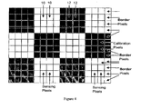
- the pixels situated at the edge of the sensor are not used, either for sensing or calibration. These have neighbouring pixels on less than four sides, whereas the other pixels have neighbours in four sides. Also, practical issues with the fabrication processing of the sensor cause variations in the size of the patterned features which will be exacerbated at the edges. These factors change the analogue performance of the 'border' pixels at the edges, and thus the border pixels are best ignored.
- Figure 2 shows an interleaving scheme using 2x2 blocks of pixels.
- interleaving in blocks does pose problems. It is reasonable to assume that an edge pixel of a block will have a response significantly different to interior pixels and should be discarded. Thus, the Figure 2 array may not be practicable.
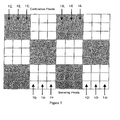
- Figure 3 shows an array interleaved in blocks of 3x3 in which, if the edge pixels are not used, only 1/9 of the surface area will be effective.
- Figure 4 shows 4x4 blocks, in which 1/4 of the area will be effective if edge pixels are unused.
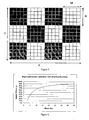
- Figure 5 shows the general case where the sensor has X (horizontally) x Y (vertically) pixels, arranged in blocks of MxN pixels. Each block therefore has (M-2) x (N-2) useful pixels.
- the graph also illustrates that the graph shows diminishing returns. With 20x20 pixels, the efficiency is 80% and increases only slowly from this point. The most useful block size is likely to lie in the range of 20-30 pixels.
- the foregoing embodiments show the blocks of sensing and calibration pixels distributed in a common-centred manner, that is in such a way that the "centre of gravity" of the two types is in a common location. This is the preferred manner, although other patterns of interleaving may be used.
- the preferred embodiments have equal numbers of sensing and calibration pixels, but the proportion of calibration pixels could be reduced while still benefiting from the underlying concept.
- a typical method of operating the sensor is as follows.
Description
- This invention relates to bio-optical sensors, that is light-sensitive semiconductor devices which detect and measure light emitted by the reaction of a reagent with a biological sample.
- In known bio-optical sensors, the reaction takes place on a surface of the semiconductor device which is an image surface divided into pixels. The light produced by reactions of this nature is small, and accordingly the signal produced by any pixel of the device is also small. The signal is frequently less than other effects such as dark current (leakage current) from the pixel, and voltage offsets. Therefore a calibration/cancellation scheme is necessary to increase the sensitivity of the system.
- In the related field of solid state image sensors there are a number of known techniques for achieving calibration. In image sensors, it is necessary to have a continuous image plane on which the image is formed. Calibration techniques involve either the use of dark frame cancellation or the use of special calibration pixels.
- In dark frame cancellation, a dark reference frame is taken and the resulting signal output is subtracted from the image frame. The dark reference frame is usually taken with the same exposure (integration time as the image but with no light impinged on the sensor, either by use of a shutter or by turning off the scene illumination.
- When calibration pixels are used, these are provided at the edge of the sensor, usually in the form of a single row or column, since it is necessary to have a continuous image surface.
- In current bio-optical sensors, a dark image is acquired before the analyte and reagents are deposited on the sensor, and this calibration image is used during detection and processing of the photo-signal. This means that there is a time difference between the acquisition of the dark reference frame and the detection and processing of the sensor signal. During this time there may be changes in the conditions on the device, e.g. operating voltage and temperature may change due to lower battery, change in ambient temperature, or self-heating due to power dissipation, and thus the calibration signal is not an accurate representation of the dark signal at the relevant time.
- An example of a current bio-optical sensor is that disclosed in
US 6,649,357 to Bryan et al. This discloses a bio-optical sensor comprising a semiconductor substrate having an image plane formed as an array of pixels, the image plane being adapted to receive thereon an analyte and a reagent which reacts with the analyte to produce light. - An object of the present invention is to provide a bio-optical sensor having a more accurate calibration signal. This increases system sensitivity and enables the system to function with less analyte, less reagent, or in a shorter time.
- Accordingly, the invention provides a bio-optical sensor comprising a semiconductor substrate having an image plane formed as an array of pixels, the image plane being adapted to receive thereon an analyte and a reagent which reacts with the analyte to produce light; in which the pixels comprise sensing pixels which generate signals which are a function of light emitted by said reaction and calibration pixels overlaid with an opaque substance so that they are not exposed to said light; and in which the calibration pixels are interleaved with the sensing pixels.
- Preferred features and other advantages of the invention will be apparent from the following description and from the claims.
- Embodiments of the invention will now be described, by way of example only, with reference to the drawings, in which:
-
Figure 1 is a schematic plan view of the image area of one embodiment of the invention; -
Figures 2 ,3 and4 are similar views of further embodiments; -
Figure 5 illustrates a general case of the image area; and -
Figure 6 is a graph showing the relationship between the size of pixel blocks and spatial efficiency. -
Figure 1 shows the simplest form of the invention in which the image surface is divided intosensing pixels 10 andcalibration pixels 12 which are interleaved on a 1:1 basis or chequerboard fashion. Each of thepixels calibration pixels 12 are shielded from light by a suitable mask, which may for example be printed on top of the array or may be formed by selective metallisation during fabrication. Where a metal mask is used, this is preferably as a layer separated from the readout electronics, to reduce parasitic capacitance. - Alternatives to metallisation to form the opaque layer include silicided gate oxide, and superposition of colour filters, i.e. overlaying red green and blue filters to give black.
- It is preferable that the pixels situated at the edge of the sensor are not used, either for sensing or calibration. These have neighbouring pixels on less than four sides, whereas the other pixels have neighbours in four sides. Also, practical issues with the fabrication processing of the sensor cause variations in the size of the patterned features which will be exacerbated at the edges. These factors change the analogue performance of the 'border' pixels at the edges, and thus the border pixels are best ignored.
- In the arrangement of
Figure 1 it will almost certainly be necessary in practical terms to cover the whole of the sensing surface with analyte and reagent, since it would be difficult to physically contain a liquid system to single pixel areas. This has the disadvantage that only 50% of the analyte and reagent is available to the sensing pixels, while the quantities of both are usually limited by problems obtaining sample and the costs of reagent. - This problem can be addressed by dividing the surface into sensitive regions and calibration regions, giving the possibility of applying the analyte and reagent only to the sensitive regions.
-
Figure 2 shows an interleaving scheme using 2x2 blocks of pixels. However, interleaving in blocks does pose problems. It is reasonable to assume that an edge pixel of a block will have a response significantly different to interior pixels and should be discarded. Thus, theFigure 2 array may not be practicable.Figure 3 shows an array interleaved in blocks of 3x3 in which, if the edge pixels are not used, only 1/9 of the surface area will be effective.Figure 4 shows 4x4 blocks, in which 1/4 of the area will be effective if edge pixels are unused. -
Figure 5 shows the general case where the sensor has X (horizontally) x Y (vertically) pixels, arranged in blocks of MxN pixels. Each block therefore has (M-2) x (N-2) useful pixels. The graph ofFigure 6 shows the percentage of useful pixels for different block sizes, assuming square blocks with M=N. - If we define

thenFigure 6 shows that with block sizes of 6x6 or less the spatial efficiency is less than 50%, i.e. worse than the simple 1x1 interleave form. For 7x7 blocks, spatial efficiency is greater than 50%, i.e. there is an improvement over the 1x1 form. - The graph also illustrates that the graph shows diminishing returns. With 20x20 pixels, the efficiency is 80% and increases only slowly from this point. The most useful block size is likely to lie in the range of 20-30 pixels.
- The foregoing embodiments show the blocks of sensing and calibration pixels distributed in a common-centred manner, that is in such a way that the "centre of gravity" of the two types is in a common location. This is the preferred manner, although other patterns of interleaving may be used.
- Likewise, the preferred embodiments have equal numbers of sensing and calibration pixels, but the proportion of calibration pixels could be reduced while still benefiting from the underlying concept.
- A typical method of operating the sensor is as follows.
- 1. Obtain image with no analyte/reagent present and no light produced: "Idark(x,y)"
- 2. Separate the image data into two images, pixel data "Pdark(x,y)" and calibration data "Cdark(x,y)"
- 3. Add the analyte/reagent and obtain an image with light Ilight(x,y)"
- 4. Separate this into two images, pixel data "Plight(x,y)" and calibration data "Clight(x,y)"
- 5. The uncompensated image is then calculated by Plight(x,y) - Pdark(x,y) (on a pixel basis)
- 6. The compensation signal is calculated from the calibration pixels as fnCal(Clight(x,y),Cdark(x,y))
- 7. Compute compensated image

- In the simplest case, fnCal could be linear, i.e. fnCal(x,y) = Cdark(x,y)/Clight(x,y). This is suitable where the error source changes linearly.
- However, the main use for this technique is to correct for temperature where the dark current rises exponentially with temperature. The calibration function can represent this, e.g.

- Depending on the design of the sense node, other errors may be significant and require a change to the calibration function. This can be computed arithmetically or determined empirically and incorporated in a look-up table.
Claims (9)
- A bio-optical sensor comprising a semiconductor substrate having an image plane formed as an array of pixels, the image plane being adapted to receive thereon an analyte and a reagent which reacts with the analyte to produce light; characterised in that:the pixels comprise sensing pixels (10) which generate signals which are a function of light emitted by said reaction and calibration pixels (12) overlaid with an opaque substance so that they are not exposed to said light; and in which the calibration pixels (12) are interleaved with the sensing pixels (10).
- A sensor according to claim 1, in which there are equal numbers of calibration pixels (12) and sensing pixels (10).
- A sensor according to claim 2, in which the pixels (10,12) are interleaved alternately.
- A sensor according to claim 1 or claim 2, in which the pixels are arranged in blocks of calibration pixels (12) and blocks of sensing pixels (10), the blocks being interleaved.
- A sensor according to claim 4, in which the signals from pixels (10,12) at the edge of a block are not used.
- A sensor according to claim 4 or claim 5, in which each block comprises between 20 and 30 pixels (10,12).
- A sensor according to any preceding claim, in which the signals from pixels (10,12) at the edge of the array are not used.
- A sensor according to any preceding claim, in which the opaque substance is formed by a metallised layer.
- A sensor according to any preceding claim, in which the surface of the image plane is divided such that the analyte and the reagent contact the sensing pixels but do not contact the calibration pixels.
Priority Applications (3)
| Application Number | Priority Date | Filing Date | Title |
|---|---|---|---|
| DE60320814T DE60320814D1 (en) | 2003-12-19 | 2003-12-19 | Bio-optical sensors |
| EP03258086A EP1544602B1 (en) | 2003-12-19 | 2003-12-19 | Bio-optical sensors |
| US11/015,242 US7447385B2 (en) | 2003-12-19 | 2004-12-17 | Bio-optical sensors |
Applications Claiming Priority (1)
| Application Number | Priority Date | Filing Date | Title |
|---|---|---|---|
| EP03258086A EP1544602B1 (en) | 2003-12-19 | 2003-12-19 | Bio-optical sensors |
Publications (2)
| Publication Number | Publication Date |
|---|---|
| EP1544602A1 EP1544602A1 (en) | 2005-06-22 |
| EP1544602B1 true EP1544602B1 (en) | 2008-05-07 |
Family
ID=34486444
Family Applications (1)
| Application Number | Title | Priority Date | Filing Date |
|---|---|---|---|
| EP03258086A Expired - Fee Related EP1544602B1 (en) | 2003-12-19 | 2003-12-19 | Bio-optical sensors |
Country Status (3)
| Country | Link |
|---|---|
| US (1) | US7447385B2 (en) |
| EP (1) | EP1544602B1 (en) |
| DE (1) | DE60320814D1 (en) |
Families Citing this family (7)
| Publication number | Priority date | Publication date | Assignee | Title |
|---|---|---|---|---|
| EP1544602B1 (en) * | 2003-12-19 | 2008-05-07 | STMicroelectronics Limited | Bio-optical sensors |
| EP1971129A1 (en) | 2007-03-16 | 2008-09-17 | STMicroelectronics (Research & Development) Limited | Improvements in or relating to image sensors |
| US8384041B2 (en) | 2010-07-21 | 2013-02-26 | Carestream Health, Inc. | Digital radiographic imaging arrays with reduced noise |
| US10345154B2 (en) * | 2015-07-17 | 2019-07-09 | Melexis Technologies Nv | Infrared sensing devices and methods |
| GB201512492D0 (en) * | 2015-07-17 | 2015-08-19 | Melexis Technologies Nv | Infrared sensing devices and methods |
| WO2017132172A1 (en) * | 2016-01-28 | 2017-08-03 | Siemens Healthcare Diagnostics Inc. | Methods and apparatus for imaging a specimen container and/or specimen using multiple exposures |
| US11630062B2 (en) * | 2019-10-10 | 2023-04-18 | Visera Technologies Company Limited | Biosensor and method of forming the same |
Family Cites Families (12)
| Publication number | Priority date | Publication date | Assignee | Title |
|---|---|---|---|---|
| US5096807A (en) * | 1985-03-06 | 1992-03-17 | Murex Corporation | Imaging immunoassay detection system with background compensation and its use |
| US5194393A (en) * | 1989-11-21 | 1993-03-16 | Bayar Aktiengesellschaft | Optical biosensor and method of use |
| AU741076B2 (en) * | 1996-12-12 | 2001-11-22 | Prolume, Ltd. | Apparatus and method for detecting and identifying infectious agents |
| US6278523B1 (en) * | 1998-02-13 | 2001-08-21 | Centre National De La Recherche Scientifique-Cnrs | Optical sensor on a silicon substrate and application for the in situ measurement of a fluorescent marker in the small bronchia |
| DE19914279C1 (en) * | 1999-03-25 | 2000-09-07 | Jena Optronik Gmbh | Sensor for optical examination of stimulated sample pixels on e.g. nano-titration screening plates or bio-chips for gene analysis, employs e.g. a liquid crystal matrix shutter and fiber optics with photomultiplier detection |
| US6583416B1 (en) * | 1999-11-15 | 2003-06-24 | Sarnoff Corporation | Uncooled IR detector array having improved temperature stability and reduced fixed pattern noise |
| CN1443305A (en) * | 2000-07-21 | 2003-09-17 | 维尔有限公司 | Coupling elements for surface plasmon resonance sensors |
| US20020115224A1 (en) * | 2001-02-16 | 2002-08-22 | Ulrich Rudel | Method for the preparation of optical (bio)chemical sensor devices |
| EP1406311B1 (en) * | 2002-10-02 | 2008-07-23 | STMicroelectronics Limited | Methods and apparatus for sensor alignment |
| EP1544602B1 (en) * | 2003-12-19 | 2008-05-07 | STMicroelectronics Limited | Bio-optical sensors |
| DE60315691D1 (en) * | 2003-12-22 | 2007-09-27 | Sgs Thomson Microelectronics | Method of producing sensors with barriers of photoresist material |
| US7286210B2 (en) * | 2003-12-31 | 2007-10-23 | Pettit John W | Passive optical sensor using carbon nanotubes |
-
2003
- 2003-12-19 EP EP03258086A patent/EP1544602B1/en not_active Expired - Fee Related
- 2003-12-19 DE DE60320814T patent/DE60320814D1/en not_active Expired - Fee Related
-
2004
- 2004-12-17 US US11/015,242 patent/US7447385B2/en not_active Expired - Fee Related
Also Published As
| Publication number | Publication date |
|---|---|
| DE60320814D1 (en) | 2008-06-19 |
| US20050141058A1 (en) | 2005-06-30 |
| EP1544602A1 (en) | 2005-06-22 |
| US7447385B2 (en) | 2008-11-04 |
Similar Documents
| Publication | Publication Date | Title |
|---|---|---|
| EP0173413B1 (en) | Color image sensor | |
| US6178254B1 (en) | Method for elimination of effects of imperfections on color measurements | |
| EP1544602B1 (en) | Bio-optical sensors | |
| US20200348424A1 (en) | Radiation imaging apparatus and radiation imaging system | |
| US7193217B2 (en) | X-ray detector | |
| JP2005322908A (en) | Monolithic x-rays detector having detection area of staggered arrangement | |
| US10564098B2 (en) | Image capture for large analyte arrays | |
| CN107958186B (en) | Electronic device | |
| JP2004533122A (en) | Wide dynamic range digital imaging system and method | |
| US20220130879A1 (en) | Image sensor and imaging apparatus | |
| JP3869952B2 (en) | Photoelectric conversion device and X-ray imaging device using the same | |
| CN1384658A (en) | Photosensitive sensor unit for image scanner to improve its spectral accuracy and raise bit depth | |
| JPS60232542A (en) | Display device for photographic picture information | |
| CN210573815U (en) | Electronic device | |
| WO2002103333B1 (en) | Method of high throughput haze screening of material | |
| CN112188126B (en) | Imaging system with self-test black level correction and correction method | |
| US20210302229A1 (en) | Method of reading the result of an electophoretic assay comprising a digital image indicating the intensity of light emitted by chemiluminescence from the output medium of the electrophoretic assay | |
| CN112889085A (en) | Saturation avoidance in digital imaging | |
| CN115000109A (en) | Ray detector and ray detection equipment | |
| CN101088163A (en) | Image sensor with globally separate colour zones | |
| JP2001340331A (en) | Radiographic device | |
| JP3548389B2 (en) | Image reading device | |
| JP4660086B2 (en) | Solid-state image sensor | |
| Burns | Image signal modulation and noise characteristics of charge-coupled device imagers | |
| JP2005117219A (en) | X-ray radiographic apparatus |
Legal Events
| Date | Code | Title | Description |
|---|---|---|---|
| PUAI | Public reference made under article 153(3) epc to a published international application that has entered the european phase |
Free format text: ORIGINAL CODE: 0009012 |
|
| AK | Designated contracting states |
Kind code of ref document: A1 Designated state(s): AT BE BG CH CY CZ DE DK EE ES FI FR GB GR HU IE IT LI LU MC NL PT RO SE SI SK TR |
|
| AX | Request for extension of the european patent |
Extension state: AL LT LV MK |
|
| 17P | Request for examination filed |
Effective date: 20051208 |
|
| AKX | Designation fees paid |
Designated state(s): DE FR GB IT |
|
| GRAP | Despatch of communication of intention to grant a patent |
Free format text: ORIGINAL CODE: EPIDOSNIGR1 |
|
| GRAS | Grant fee paid |
Free format text: ORIGINAL CODE: EPIDOSNIGR3 |
|
| GRAA | (expected) grant |
Free format text: ORIGINAL CODE: 0009210 |
|
| AK | Designated contracting states |
Kind code of ref document: B1 Designated state(s): DE FR GB IT |
|
| REG | Reference to a national code |
Ref country code: GB Ref legal event code: FG4D |
|
| REF | Corresponds to: |
Ref document number: 60320814 Country of ref document: DE Date of ref document: 20080619 Kind code of ref document: P |
|
| RAP2 | Party data changed (patent owner data changed or rights of a patent transferred) |
Owner name: STMICROELECTRONICS (RESEARCH & DEVELOPMENT) LIMITE |
|
| PLBE | No opposition filed within time limit |
Free format text: ORIGINAL CODE: 0009261 |
|
| STAA | Information on the status of an ep patent application or granted ep patent |
Free format text: STATUS: NO OPPOSITION FILED WITHIN TIME LIMIT |
|
| 26N | No opposition filed |
Effective date: 20090210 |
|
| PG25 | Lapsed in a contracting state [announced via postgrant information from national office to epo] |
Ref country code: IT Free format text: LAPSE BECAUSE OF FAILURE TO SUBMIT A TRANSLATION OF THE DESCRIPTION OR TO PAY THE FEE WITHIN THE PRESCRIBED TIME-LIMIT Effective date: 20080507 |
|
| PG25 | Lapsed in a contracting state [announced via postgrant information from national office to epo] |
Ref country code: DE Free format text: LAPSE BECAUSE OF NON-PAYMENT OF DUE FEES Effective date: 20090701 |
|
| PGFP | Annual fee paid to national office [announced via postgrant information from national office to epo] |
Ref country code: GB Payment date: 20141126 Year of fee payment: 12 |
|
| REG | Reference to a national code |
Ref country code: FR Ref legal event code: PLFP Year of fee payment: 13 |
|
| GBPC | Gb: european patent ceased through non-payment of renewal fee |
Effective date: 20151219 |
|
| PG25 | Lapsed in a contracting state [announced via postgrant information from national office to epo] |
Ref country code: GB Free format text: LAPSE BECAUSE OF NON-PAYMENT OF DUE FEES Effective date: 20151219 |
|
| REG | Reference to a national code |
Ref country code: FR Ref legal event code: PLFP Year of fee payment: 14 |
|
| REG | Reference to a national code |
Ref country code: FR Ref legal event code: PLFP Year of fee payment: 15 |
|
| PGFP | Annual fee paid to national office [announced via postgrant information from national office to epo] |
Ref country code: FR Payment date: 20191120 Year of fee payment: 17 |
|
| PG25 | Lapsed in a contracting state [announced via postgrant information from national office to epo] |
Ref country code: FR Free format text: LAPSE BECAUSE OF NON-PAYMENT OF DUE FEES Effective date: 20201231 |