EP1553692B1 - Method for determining output currents of frequency converter - Google Patents
Method for determining output currents of frequency converter Download PDFInfo
- Publication number
- EP1553692B1 EP1553692B1 EP04106635A EP04106635A EP1553692B1 EP 1553692 B1 EP1553692 B1 EP 1553692B1 EP 04106635 A EP04106635 A EP 04106635A EP 04106635 A EP04106635 A EP 04106635A EP 1553692 B1 EP1553692 B1 EP 1553692B1
- Authority
- EP
- European Patent Office
- Prior art keywords
- frequency converter
- vector
- modulation sequence
- modulation
- voltage
- Prior art date
- Legal status (The legal status is an assumption and is not a legal conclusion. Google has not performed a legal analysis and makes no representation as to the accuracy of the status listed.)
- Active
Links
- 238000000034 method Methods 0.000 title claims abstract description 40
- 239000013598 vector Substances 0.000 claims abstract description 116
- 238000005259 measurement Methods 0.000 claims description 21
- 230000008859 change Effects 0.000 description 9
- 230000004907 flux Effects 0.000 description 5
- 230000008569 process Effects 0.000 description 5
- 230000008878 coupling Effects 0.000 description 4
- 238000010168 coupling process Methods 0.000 description 4
- 238000005859 coupling reaction Methods 0.000 description 4
- 238000005070 sampling Methods 0.000 description 3
- 238000012545 processing Methods 0.000 description 2
- 230000005355 Hall effect Effects 0.000 description 1
- 230000008901 benefit Effects 0.000 description 1
- 239000003990 capacitor Substances 0.000 description 1
- 238000007796 conventional method Methods 0.000 description 1
- 230000001419 dependent effect Effects 0.000 description 1
- 238000005516 engineering process Methods 0.000 description 1
- 238000012423 maintenance Methods 0.000 description 1
- 238000000691 measurement method Methods 0.000 description 1
- 230000010363 phase shift Effects 0.000 description 1
- 239000000243 solution Substances 0.000 description 1
- 239000012086 standard solution Substances 0.000 description 1
Images

Classifications
-
- H—ELECTRICITY
- H02—GENERATION; CONVERSION OR DISTRIBUTION OF ELECTRIC POWER
- H02P—CONTROL OR REGULATION OF ELECTRIC MOTORS, ELECTRIC GENERATORS OR DYNAMO-ELECTRIC CONVERTERS; CONTROLLING TRANSFORMERS, REACTORS OR CHOKE COILS
- H02P27/00—Arrangements or methods for the control of AC motors characterised by the kind of supply voltage
- H02P27/04—Arrangements or methods for the control of AC motors characterised by the kind of supply voltage using variable-frequency supply voltage, e.g. inverter or converter supply voltage
- H02P27/06—Arrangements or methods for the control of AC motors characterised by the kind of supply voltage using variable-frequency supply voltage, e.g. inverter or converter supply voltage using dc to ac converters or inverters
- H02P27/08—Arrangements or methods for the control of AC motors characterised by the kind of supply voltage using variable-frequency supply voltage, e.g. inverter or converter supply voltage using dc to ac converters or inverters with pulse width modulation
- H02P27/12—Arrangements or methods for the control of AC motors characterised by the kind of supply voltage using variable-frequency supply voltage, e.g. inverter or converter supply voltage using dc to ac converters or inverters with pulse width modulation pulsing by guiding the flux vector, current vector or voltage vector on a circle or a closed curve, e.g. for direct torque control
-
- H—ELECTRICITY
- H02—GENERATION; CONVERSION OR DISTRIBUTION OF ELECTRIC POWER
- H02M—APPARATUS FOR CONVERSION BETWEEN AC AND AC, BETWEEN AC AND DC, OR BETWEEN DC AND DC, AND FOR USE WITH MAINS OR SIMILAR POWER SUPPLY SYSTEMS; CONVERSION OF DC OR AC INPUT POWER INTO SURGE OUTPUT POWER; CONTROL OR REGULATION THEREOF
- H02M7/00—Conversion of ac power input into dc power output; Conversion of dc power input into ac power output
- H02M7/42—Conversion of dc power input into ac power output without possibility of reversal
- H02M7/44—Conversion of dc power input into ac power output without possibility of reversal by static converters
- H02M7/48—Conversion of dc power input into ac power output without possibility of reversal by static converters using discharge tubes with control electrode or semiconductor devices with control electrode
- H02M7/53—Conversion of dc power input into ac power output without possibility of reversal by static converters using discharge tubes with control electrode or semiconductor devices with control electrode using devices of a triode or transistor type requiring continuous application of a control signal
- H02M7/537—Conversion of dc power input into ac power output without possibility of reversal by static converters using discharge tubes with control electrode or semiconductor devices with control electrode using devices of a triode or transistor type requiring continuous application of a control signal using semiconductor devices only, e.g. single switched pulse inverters
- H02M7/5387—Conversion of dc power input into ac power output without possibility of reversal by static converters using discharge tubes with control electrode or semiconductor devices with control electrode using devices of a triode or transistor type requiring continuous application of a control signal using semiconductor devices only, e.g. single switched pulse inverters in a bridge configuration
-
- H—ELECTRICITY
- H02—GENERATION; CONVERSION OR DISTRIBUTION OF ELECTRIC POWER
- H02M—APPARATUS FOR CONVERSION BETWEEN AC AND AC, BETWEEN AC AND DC, OR BETWEEN DC AND DC, AND FOR USE WITH MAINS OR SIMILAR POWER SUPPLY SYSTEMS; CONVERSION OF DC OR AC INPUT POWER INTO SURGE OUTPUT POWER; CONTROL OR REGULATION THEREOF
- H02M1/00—Details of apparatus for conversion
- H02M1/0003—Details of control, feedback or regulation circuits
- H02M1/0009—Devices or circuits for detecting current in a converter
-
- H—ELECTRICITY
- H02—GENERATION; CONVERSION OR DISTRIBUTION OF ELECTRIC POWER
- H02M—APPARATUS FOR CONVERSION BETWEEN AC AND AC, BETWEEN AC AND DC, OR BETWEEN DC AND DC, AND FOR USE WITH MAINS OR SIMILAR POWER SUPPLY SYSTEMS; CONVERSION OF DC OR AC INPUT POWER INTO SURGE OUTPUT POWER; CONTROL OR REGULATION THEREOF
- H02M7/00—Conversion of ac power input into dc power output; Conversion of dc power input into ac power output
- H02M7/42—Conversion of dc power input into ac power output without possibility of reversal
- H02M7/44—Conversion of dc power input into ac power output without possibility of reversal by static converters
- H02M7/48—Conversion of dc power input into ac power output without possibility of reversal by static converters using discharge tubes with control electrode or semiconductor devices with control electrode
- H02M7/53—Conversion of dc power input into ac power output without possibility of reversal by static converters using discharge tubes with control electrode or semiconductor devices with control electrode using devices of a triode or transistor type requiring continuous application of a control signal
- H02M7/537—Conversion of dc power input into ac power output without possibility of reversal by static converters using discharge tubes with control electrode or semiconductor devices with control electrode using devices of a triode or transistor type requiring continuous application of a control signal using semiconductor devices only, e.g. single switched pulse inverters
- H02M7/539—Conversion of dc power input into ac power output without possibility of reversal by static converters using discharge tubes with control electrode or semiconductor devices with control electrode using devices of a triode or transistor type requiring continuous application of a control signal using semiconductor devices only, e.g. single switched pulse inverters with automatic control of output wave form or frequency
- H02M7/5395—Conversion of dc power input into ac power output without possibility of reversal by static converters using discharge tubes with control electrode or semiconductor devices with control electrode using devices of a triode or transistor type requiring continuous application of a control signal using semiconductor devices only, e.g. single switched pulse inverters with automatic control of output wave form or frequency by pulse-width modulation
Definitions
- the present invention relates to a method according to the preamble of claim 1.
- Vector control containing no motion sensor is a manner of controlling electric motor drives fed by a frequency converter which is about to become a standard solution. It provides a vast majority of applications with sufficient performance without the drawbacks caused by velocity feedback, including e.g. cost inflicted by the encoder used for feedback, mounting and cabling costs as well as service and maintenance.
- vector control without motion sensors is based on measuring two or three output phase currents of a frequency converter.
- the measurement is implemented e.g. by current transducers based on the Hall effect, in which case the costs, need for space and the number of components of the method are extensive in connection with low-power frequency converters in particular. Making current measurement a simpler process enables savings to be achieved in terms of costs, need for space as well as the number of components; however, maintaining the performance level of the control method becomes a challenge.
- a reference value is calculated for a voltage vector so as to achieve a certain electromagnetic state for a motor to be controlled.
- a voltage reference determines the direction and magnitude of the voltage vector necessary during a modulation sequence.
- a modulator calculates switch references, i.e. the times for the states of each power switch used during a modulation sequence.
- An inverter part of a three-phase frequency converter comprises three pairs of switches, each switch pair being coupled in series between a positive and a negative busbar of a voltage intermediate circuit of the frequency converter. A point between the switch pairs constitutes a phase output of an inverter such that each phase may provide the output either with positive or negative voltage of the intermediate circuit.
- the output voltage provided by switches is usually regarded as a complex-plane voltage vector.
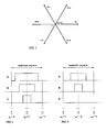
- Switch pairs may be used for forming six voltage vectors which deviate from zero and which reside in a complex plane at a mutual 60 degree phase shift such that by coupling the output of phase A to be positive and the outputs of other phases B, C to be negative, a voltage vector +-- is obtained which resides in a direction parallel to a positive real axis of the complex plane, as shown in Figure 1 .
- Other voltage vectors are designated in a similar manner, e.g.
- a voltage vector -+- is a vector obtained when the output of phase B is coupled to a positive busbar of the voltage intermediate circuit while the output of other phases A, C is coupled to a negative busbar thereof.
- a voltage vector -+- is a vector obtained when the output of phase B is coupled to a positive busbar of the voltage intermediate circuit while the output of other phases A, C is coupled to a negative busbar thereof.
- a voltage reference is implemented by calculating the time each switch combination is to be used in order to achieve the voltage reference during a modulation sequence.
- the simplest presently conceivable manner of measuring current so as to ensure the operation of vector control is to measure the current passing through the positive or the negative busbar of an intermediate circuit.
- This DC current measurement can be implemented e.g. by means of a shunt resistance situated in a busbar of the intermediate circuit, whose voltage drop is proportional to the current passing through the busbar. All current to an inverter part of a frequency converter passes via the intermediate circuit, which means that by measuring the current of the intermediate circuit, the current of one phase that is flowing to the load at a given moment is achieved.
- DC current measurement enables short-circuit protection to be implemented without any additional measurement electronics.
- the conventional three-phase modulation method disclosed above is problematic, since both at a beginning and at an end of a modulation sequence as well as in a middle thereof, a zero vector is used during which the DC current is zero in size and contains no phase current information.
- DC current sampling should take place at a moment in dependence on a modulation index, and thus changing from a modulation sequence to another, so that a voltage vector deviating from zero would then be in use and phase current information would thus exist, which, as far as the implementation in practice is concerned, would be problematic.
- Current measurement may also be implemented such that DC current is sampled at a high frequency, relying on getting a necessary number of phase currents measured in order to maintain reliability.
- such a method requires numerous samples to be taken and a considerable processing capacity in order to allocate these samples into currents of different phases on the basis of switch positions, for example.
- An object of the present invention is to provide a method which solves the above-disclosed problem and enables current information on a frequency converter to be determined in a simpler manner. This object is achieved by a method according to the characterizing part of claim 1. Preferred embodiments of the invention are disclosed in the dependent claims.
- the idea underlying the invention is that output switches of an inverter part of a three-phase frequency converter are modulated in a two-phase manner, which enables a voltage vector deviating from a zero vector to be produced at a predetermined location in a modulation sequence. Furthermore, changing the zero vector to be used in the modulation sequence enables DC current information on two phases to be measured in a reliable manner. This enables a reliable manner of measuring two phase currents as often as necessary also at very low output frequencies of the frequency converter.
- Two-phase modulation means that during one modulation sequence, the state of the switches of only two output phases is changed in order to achieve a desired voltage vector while the switch position of the third phase remains unchanged during the entire modulation sequence.
- An advantage of the method of the invention is that when two-phase modulation is utilized, a voltage vector deviating from a zero vector is in use either at a beginning or at an end of a modulation sequence or in a middle thereof; this makes it possible to measure one phase current.
- Two-phase modulation thus enables one phase current to be measured during each modulation sequence at a constant-remaining moment in dependence on the modulation sequence.
- a change of the zero vector according to the method of the invention enables the phase currents of two phases to be determined.
- Figure 1 shows a voltage vector star
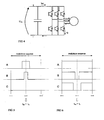
- Figure 2 shows a conventional three-phase modulation pattern
- Figure 3 shows a two-phase modulation pattern
- Figure 4 shows a schematic description of an inverter part of a frequency converter
- Figure 5 shows a two-phase modulation pattern
- Figure 6 shows a two-phase modulation pattern implementing the same average voltage vector as the modulation pattern of Figure 5 , utilizing an opposite zero voltage vector;
- Figure 7 shows a two-phase modulation pattern
- Figure 8 shows a two-phase modulation pattern implementing the same average voltage vector as the modulation pattern of Figure 7 , utilizing an opposite zero voltage vector;
- Figure 9 shows an example of a control system wherein the method according to the invention may be utilized.
- FIG. 4 schematically shows an inverter part of a three-phase frequency converter.
- the inverter part comprises a voltage intermediate circuit U dc and power switch pairs constituting an output of the frequency converter. These switch pairs are coupled in series between a positive + and a negative - busbar of the voltage intermediate circuit so that a midpoint of each switch pair constitutes an output of phase A, B, C of the frequency converter.
- a voltage vector reference is formed for the output power switches such that only two switch pairs are modulated during one modulation sequence.
- a modulation sequence refers to a time sequence which constitutes an average inverter switching frequency.
- an output is provided with an average voltage vector according to a reference received from a higher level of the control circuit.
- the voltage vector is formed in a manner known per se by using the vectors shown in Figure 1 .
- said two switch pairs are controlled to implement a voltage reference vector during the modulation sequence by using one zero vector.
- Figure 3 shows an example of one modulation sequence of two-phase modulation, wherein switchings are thus carried out in two phases only.
- the state of the switch pairs of phases A and B is changed from negative to positive and further to negative.
- the output switches implement a voltage vector ---, i.e. a zero vector, during which no current passes via the intermediate circuit of the frequency converter through the switches to the load.
- the voltage vector of the output changes into a vector +-- and further, after the coupling of phase B, into a vector ++-.
- This switch position is also used in the middle of the modulation sequence. After this moment, the vector pattern is repeated, symmetrically with respect to the midpoint of the modulation sequence till the end of the modulation sequence. As can be seen in Figure 3 , the state of phase C does not change at all during the entire modulation sequence.
- Figure 2 shows a conventional three-phase modulation pattern.
- An average voltage vector produced during a modulation sequence by this modulation pattern corresponds with the voltage vector produced by the two-phase modulation of Figure 3 .
- the current of the voltage intermediate circuit of the frequency converter is measured at a predetermined moment in the modulation sequence.
- Figure 4 schematically shows a structure of an inverter part of a frequency converter, disclosing how currents pass in the middle of the modulation sequence of Figure 3 , i.e. during the voltage vector ++-.
- the arrows in Figure 4 show that the current in the intermediate circuit passes via phases A and B to the load, and further through the load via a lower branch of phase C back to the intermediate circuit. Since use of two-phase modulation enables the exact moment at which the zero vector is not in use to be determined, the current of one phase of the load can be measured accurately. This particular moment to be determined is completely independent of both the magnitude and direction of the average voltage vector to be produced.
- This predetermined moment is in dependence on the modulation sequence and resides in a middle thereof.
- phase current can be measured.
- the modulation pattern may be changed so as to enable the necessary current information to be measured at some other moment in dependence on a modulation sequence.
- a moment is e.g. a beginning or an end of a modulation sequence, i.e. the moment when one modulation sequence changes into a next modulation sequence.
- the zero vectors to be used in modulation sequences during use of a frequency converter are changed actively. Since current information on all output phases of the frequency converter is to be obtained frequently enough as far as control is concerned, the zero vector to be used should, according to the invention, be changed on a regular basis between the modulation sequences. Changing the zero vector does not affect the magnitude of an average voltage vector obtained during a modulation sequence but all voltage vectors can be implemented by two-phase modulation, using either one of the zero vectors +++ or - --. Due to the changing of the zero vector, the modulation pattern alters, and at the same time, the voltage vector being used at a predetermined current measurement moment changes.
- Figures 5 and 6 show two-phase modulation patterns implementing the same average voltage vector during a modulation sequence.
- a zero vector --- is used at a beginning and at an end of the modulation sequence.
- a voltage vector ++- is used, during which current -i C can be measured from an intermediate circuit.
- a modulation pattern is used wherein the zero vector is a vector +++.
- a voltage vector +-- is then used in a middle of a modulation sequence.
- the current of an intermediate circuit measured during the voltage vector +-- corresponds with current i A , i.e. the output current of phase A.
- the method of the invention enables the current of two different phases to be measured by changing actively the zero vector to be used.
- Current samples of all three phases can be measured as a voltage vector reference changes between sectors. It is not, however, necessary to obtain the current information on all three phases in order to ensure the operation of a controlled drive.
- Figures 5 and 6 show successive modulation sequences implementing the same average voltage during the modulation sequences by using different zero vectors. It is to be noted that when the process moves from Figure 5 to Figure 6 , the state of all switches is to be changed simultaneously. Naturally, this is not desirable since simultaneous turns of the switches may cause problems.
- Figures 7 and 8 disclose a solution wherein a zero vector is changed by controlling one switch pair only.
- Figure 7 shows a modulation pattern corresponding with that of Figure 5 wherefrom, according to the invention, the process is to move to a modulation pattern employing an opposite zero voltage vector.
- a modulation pattern forming such a zero vector is shown in Figure 8 wherein a switch of phase A is in a high, i.e. +, position during the entire modulation sequence.
- a switch of phase B is controlled first and last, prior to a middle point of the modulation sequence, a switch of phase C.
- a voltage vector formed by the modulation pattern of Figure 8 during the modulation sequence corresponds with the voltage vector formed by Figure 7 , and the zero vector used is a different one from that used in the modulation of Figure 7 .
- a second preferred alternative in order to obtain relevant current information is to change the sampling moment in dependence on the zero vector.
- the zero vector to be used determines the moments at which relevant current information is available, and measurements can be carried out at such moments only.
- the zero vector to be used is changed at intervals of two modulation sequences or less often, i.e. the same zero voltage vector is used in two or more successive modulation sequences. This should also be taken into account when processing the results of DC current measurements, so that when current measurement occurs in connection with a zero vector change and a modulation sequence change, it is not advisable to use the result of the current measurement.
- the zero voltage vector may also be changed such that the change is carried out after the changing number of modulation sequences.
- a criterion for changing the zero vector may then be e.g. the frequency of output voltage.
- the frequency When the frequency is low, when the process remains in the same voltage sector for a long time, a change should take place frequently enough in order to obtain measurement information on two phase currents.
- the zero voltage vector can be changed less often or changing the zero vector actively may be even stopped.
- the zero vector When operating in accordance with the invention, the zero vector may be changed in various different ways. The point is that the zero vector is changed as often as necessary at low frequencies in order to obtain current information on at least two phases, and that the same zero vector is used successively during at least two modulation sequences in order to ensure the correctness of the current information.
- Figure 9 shows a control method utilizing estimated motor currents, wherein current estimates are formed e.g. by means of inverter switch positions Sa, Sb, Sc, measured intermediate circuit voltage U dc and motor parameters in a manner known per se. Since motor parameters and measured/known variables contain error, current estimates to be obtained have to be corrected by means of the measured current information.
- This measured current information is formed by the method of the invention.
- This method being less sensitive to various interference related to measurements than a control method utilizing measurements directly, is thus advantageous to be used e.g. in an environment with interference or in connection with utilizing poor-performance current measurement equipment.
- FIG. 9 is a control method known per se, wherein a flux controller 91 receives at its input a flux reference value ⁇ ref and a flux actual value ⁇ act determined by an observer 95.
- a velocity control 92 produces a reference for a component i q,ref transverse to the current on the basis of a reference value ⁇ ref of angular velocity and actual value ⁇ act determined by the observer.
- the magnitude of the current actual value i act calculated by means of motor parameters of the observer, switch references and intermediate circuit voltage can be corrected on the basis of samples which, in the embodiment of Figure 9 , are obtained from block 96, e.g. either directly by replacing the magnitude of current calculated by the observer with the magnitude of a sample or by weighting the samples by a certain weight factor and thus correcting the value determined by the observer.
- a current sample is obtained according to the method either at a beginning/at an end or in a middle of a modulation sequence. If the current sample were taken at a random moment in a modulation sequence, as tends to be the case in connection with the conventional methods disclosed above, the sample would be useless for enabling estimated current to be corrected directly since the estimated current normally represents the actual current either at a beginning, in a middle or at an end of a modulation sequence.
- the disclosed current measurement method is particularly well suited for use together with the exemplary control principle disclosed above since measurements obtained relatively seldom and mutually non-simultaneously for different phases suffice to satisfy the needs of a control which utilizes estimates.
Abstract
Description
- The present invention relates to a method according to the preamble of claim 1.
- Vector control containing no motion sensor is a manner of controlling electric motor drives fed by a frequency converter which is about to become a standard solution. It provides a vast majority of applications with sufficient performance without the drawbacks caused by velocity feedback, including e.g. cost inflicted by the encoder used for feedback, mounting and cabling costs as well as service and maintenance.
- Typically, vector control without motion sensors is based on measuring two or three output phase currents of a frequency converter. The measurement is implemented e.g. by current transducers based on the Hall effect, in which case the costs, need for space and the number of components of the method are extensive in connection with low-power frequency converters in particular. Making current measurement a simpler process enables savings to be achieved in terms of costs, need for space as well as the number of components; however, maintaining the performance level of the control method becomes a challenge.
- In vector control, a reference value is calculated for a voltage vector so as to achieve a certain electromagnetic state for a motor to be controlled. A voltage reference determines the direction and magnitude of the voltage vector necessary during a modulation sequence. Based on this information, a modulator calculates switch references, i.e. the times for the states of each power switch used during a modulation sequence. An inverter part of a three-phase frequency converter comprises three pairs of switches, each switch pair being coupled in series between a positive and a negative busbar of a voltage intermediate circuit of the frequency converter. A point between the switch pairs constitutes a phase output of an inverter such that each phase may provide the output either with positive or negative voltage of the intermediate circuit.
- In the case of vector control, the output voltage provided by switches is usually regarded as a complex-plane voltage vector. Switch pairs may be used for forming six voltage vectors which deviate from zero and which reside in a complex plane at a mutual 60 degree phase shift such that by coupling the output of phase A to be positive and the outputs of other phases B, C to be negative, a voltage vector +-- is obtained which resides in a direction parallel to a positive real axis of the complex plane, as shown in
Figure 1 . Other voltage vectors are designated in a similar manner, e.g. a voltage vector -+- is a vector obtained when the output of phase B is coupled to a positive busbar of the voltage intermediate circuit while the output of other phases A, C is coupled to a negative busbar thereof. In connection with a three-phase frequency converter it is possible to produce eight voltage vectors, two of which being zero vectors +++ or --- that are formed by coupling the outputs of each of them either to a positive busbar (+++) or to a negative busbar (---). In vector control, a voltage reference is implemented by calculating the time each switch combination is to be used in order to achieve the voltage reference during a modulation sequence. - In a conventional three-phase modulation shown in
Figure 2 , switchings are carried out in every three phases during each modulation sequence. A modulation sequence starts from one zero vector and ends at the same zero vector, passing via another zero vector in a middle of the modulation sequence. - The simplest presently conceivable manner of measuring current so as to ensure the operation of vector control is to measure the current passing through the positive or the negative busbar of an intermediate circuit. This DC current measurement can be implemented e.g. by means of a shunt resistance situated in a busbar of the intermediate circuit, whose voltage drop is proportional to the current passing through the busbar. All current to an inverter part of a frequency converter passes via the intermediate circuit, which means that by measuring the current of the intermediate circuit, the current of one phase that is flowing to the load at a given moment is achieved. In addition to simplicity and the resulting inexpensiveness, need for less space and the small number of components, DC current measurement enables short-circuit protection to be implemented without any additional measurement electronics.
- As far as DC current measurement is concerned, the conventional three-phase modulation method disclosed above is problematic, since both at a beginning and at an end of a modulation sequence as well as in a middle thereof, a zero vector is used during which the DC current is zero in size and contains no phase current information. In order to obtain phase current information, DC current sampling should take place at a moment in dependence on a modulation index, and thus changing from a modulation sequence to another, so that a voltage vector deviating from zero would then be in use and phase current information would thus exist, which, as far as the implementation in practice is concerned, would be problematic. Current measurement may also be implemented such that DC current is sampled at a high frequency, relying on getting a necessary number of phase currents measured in order to maintain reliability. However, such a method requires numerous samples to be taken and a considerable processing capacity in order to allocate these samples into currents of different phases on the basis of switch positions, for example.
- An object of the present invention is to provide a method which solves the above-disclosed problem and enables current information on a frequency converter to be determined in a simpler manner. This object is achieved by a method according to the characterizing part of claim 1. Preferred embodiments of the invention are disclosed in the dependent claims.
- The idea underlying the invention is that output switches of an inverter part of a three-phase frequency converter are modulated in a two-phase manner, which enables a voltage vector deviating from a zero vector to be produced at a predetermined location in a modulation sequence. Furthermore, changing the zero vector to be used in the modulation sequence enables DC current information on two phases to be measured in a reliable manner. This enables a reliable manner of measuring two phase currents as often as necessary also at very low output frequencies of the frequency converter. Two-phase modulation means that during one modulation sequence, the state of the switches of only two output phases is changed in order to achieve a desired voltage vector while the switch position of the third phase remains unchanged during the entire modulation sequence.
- An advantage of the method of the invention is that when two-phase modulation is utilized, a voltage vector deviating from a zero vector is in use either at a beginning or at an end of a modulation sequence or in a middle thereof; this makes it possible to measure one phase current. Two-phase modulation thus enables one phase current to be measured during each modulation sequence at a constant-remaining moment in dependence on the modulation sequence. Furthermore, a change of the zero vector according to the method of the invention enables the phase currents of two phases to be determined.
- The invention is now described in closer detail in connection with the preferred embodiments and with reference to the accompanying drawings, in which
-
Figure 1 shows a voltage vector star; -
Figure 2 shows a conventional three-phase modulation pattern; -
Figure 3 shows a two-phase modulation pattern; -
Figure 4 shows a schematic description of an inverter part of a frequency converter; -
Figure 5 shows a two-phase modulation pattern; -
Figure 6 shows a two-phase modulation pattern implementing the same average voltage vector as the modulation pattern ofFigure 5 , utilizing an opposite zero voltage vector; -
Figure 7 shows a two-phase modulation pattern; -
Figure 8 shows a two-phase modulation pattern implementing the same average voltage vector as the modulation pattern ofFigure 7 , utilizing an opposite zero voltage vector; and -
Figure 9 shows an example of a control system wherein the method according to the invention may be utilized. -
Figure 4 schematically shows an inverter part of a three-phase frequency converter. The inverter part comprises a voltage intermediate circuit Udc and power switch pairs constituting an output of the frequency converter. These switch pairs are coupled in series between a positive + and a negative - busbar of the voltage intermediate circuit so that a midpoint of each switch pair constitutes an output of phase A, B, C of the frequency converter. - According to the method of the invention, a voltage vector reference is formed for the output power switches such that only two switch pairs are modulated during one modulation sequence. A modulation sequence refers to a time sequence which constitutes an average inverter switching frequency. In other words, during a modulation sequence an output is provided with an average voltage vector according to a reference received from a higher level of the control circuit. The voltage vector is formed in a manner known per se by using the vectors shown in
Figure 1 . - Further, according to the invention, said two switch pairs are controlled to implement a voltage reference vector during the modulation sequence by using one zero vector.
Figure 3 shows an example of one modulation sequence of two-phase modulation, wherein switchings are thus carried out in two phases only. In the exemplary case of the figure, the state of the switch pairs of phases A and B is changed from negative to positive and further to negative. At a beginning of the modulation sequence, the output switches implement a voltage vector ---, i.e. a zero vector, during which no current passes via the intermediate circuit of the frequency converter through the switches to the load. After the coupling of phase A, the voltage vector of the output changes into a vector +-- and further, after the coupling of phase B, into a vector ++-. This switch position is also used in the middle of the modulation sequence. After this moment, the vector pattern is repeated, symmetrically with respect to the midpoint of the modulation sequence till the end of the modulation sequence. As can be seen inFigure 3 , the state of phase C does not change at all during the entire modulation sequence. -
Figure 2 shows a conventional three-phase modulation pattern. An average voltage vector produced during a modulation sequence by this modulation pattern corresponds with the voltage vector produced by the two-phase modulation ofFigure 3 . It can be seen in the pattern ofFigure 2 that a zero vector +++ is provided as a voltage vector in the middle of the modulation sequence while a voltage vector ++- is provided in the middle of the modulation pattern ofFigure 3 producing a corresponding average voltage vector, in which case current iDC = -iC, i.e. the current of phase C as negative, can be measured as the DC current of the voltage intermediate circuit. - Further, according to the invention, the current of the voltage intermediate circuit of the frequency converter is measured at a predetermined moment in the modulation sequence.
Figure 4 schematically shows a structure of an inverter part of a frequency converter, disclosing how currents pass in the middle of the modulation sequence ofFigure 3 , i.e. during the voltage vector ++-. The arrows inFigure 4 show that the current in the intermediate circuit passes via phases A and B to the load, and further through the load via a lower branch of phase C back to the intermediate circuit. Since use of two-phase modulation enables the exact moment at which the zero vector is not in use to be determined, the current of one phase of the load can be measured accurately. This particular moment to be determined is completely independent of both the magnitude and direction of the average voltage vector to be produced. - Current is measured from the voltage intermediate circuit at a predetermined moment. Preferably, this predetermined moment is in dependence on the modulation sequence and resides in a middle thereof. Hence, in the case of
Figure 3 , for instance, phase current can be measured. Naturally, the modulation pattern may be changed so as to enable the necessary current information to be measured at some other moment in dependence on a modulation sequence. Such a moment is e.g. a beginning or an end of a modulation sequence, i.e. the moment when one modulation sequence changes into a next modulation sequence. - Further, according to the invention, the zero vectors to be used in modulation sequences during use of a frequency converter are changed actively. Since current information on all output phases of the frequency converter is to be obtained frequently enough as far as control is concerned, the zero vector to be used should, according to the invention, be changed on a regular basis between the modulation sequences. Changing the zero vector does not affect the magnitude of an average voltage vector obtained during a modulation sequence but all voltage vectors can be implemented by two-phase modulation, using either one of the zero vectors +++ or - --. Due to the changing of the zero vector, the modulation pattern alters, and at the same time, the voltage vector being used at a predetermined current measurement moment changes. At low output voltage frequencies in particular, it is important to change the zero vector in order to obtain the necessary current information by using DC current measurement. Changing the zero vector is known per se in connection with inverters. This technology is used e.g. for evening out component losses at low rotational speeds and for maintaining the charge of bootstrap capacitors of gate drivers.
-
Figures 5 and 6 show two-phase modulation patterns implementing the same average voltage vector during a modulation sequence. In the modulation pattern ofFigure 5 , a zero vector --- is used at a beginning and at an end of the modulation sequence. In a middle of the modulation sequence, a voltage vector ++- is used, during which current -iC can be measured from an intermediate circuit. InFigure 6 , in turn, a modulation pattern is used wherein the zero vector is a vector +++. A voltage vector +-- is then used in a middle of a modulation sequence. The current of an intermediate circuit measured during the voltage vector +-- corresponds with current iA, i.e. the output current of phase A. Thus, in the manner shown inFigures 5 and 6 , the method of the invention enables the current of two different phases to be measured by changing actively the zero vector to be used. Current samples of all three phases can be measured as a voltage vector reference changes between sectors. It is not, however, necessary to obtain the current information on all three phases in order to ensure the operation of a controlled drive. -
Figures 5 and 6 show successive modulation sequences implementing the same average voltage during the modulation sequences by using different zero vectors. It is to be noted that when the process moves fromFigure 5 to Figure 6 , the state of all switches is to be changed simultaneously. Naturally, this is not desirable since simultaneous turns of the switches may cause problems.Figures 7 and 8 disclose a solution wherein a zero vector is changed by controlling one switch pair only. -
Figure 7 shows a modulation pattern corresponding with that ofFigure 5 wherefrom, according to the invention, the process is to move to a modulation pattern employing an opposite zero voltage vector. A modulation pattern forming such a zero vector is shown inFigure 8 wherein a switch of phase A is in a high, i.e. +, position during the entire modulation sequence. A switch of phase B is controlled first and last, prior to a middle point of the modulation sequence, a switch of phase C. A voltage vector formed by the modulation pattern ofFigure 8 during the modulation sequence corresponds with the voltage vector formed byFigure 7 , and the zero vector used is a different one from that used in the modulation ofFigure 7 . It is to be noted that when forming a modulation pattern in the manner shown inFigure 8 , the zero vector resides in a middle of the modulation sequence. Consequently, a voltage vector deviating from zero resides at a beginning and at an end of the modulation sequence. - Because the location of the moment at which current information can be measured changes when the zero vector is changed between modulation sequences as shown in
Figures 7 and 8 , it is preferable to measure DC current twice during one modulation sequence, i.e. at a beginning/at an end and in a middle of a modulation sequence. In other words, a double modulation sequence frequency is obtained to be the current sampling frequency. Real relevant current samples and non-relevant samples are then obtained. From among these current samples, however, it is simple to pick samples that reflect the real magnitude of phase current. In the modulation pattern according toFigure 8 , the zero vector +++ resides in the middle of the modulation sequence. Correspondingly, the zero vector --- ofFigure 7 resides at the beginning and at the end of the modulation sequence. Based on this information, it is simple to choose a sample containing correct measurement information by software. It is to be noted, however, thatFigures 7 and 8 only show one embodiment. It is also possible to place the zero vectors the other way around in the modulation sequence, i.e. the vector +++ at the beginning/end of the modulation sequence and the vector --- in the middle thereof. - A second preferred alternative in order to obtain relevant current information is to change the sampling moment in dependence on the zero vector. In such a case, the zero vector to be used determines the moments at which relevant current information is available, and measurements can be carried out at such moments only.
- Furthermore, in connection with the method of the invention wherein a zero vector is changed, it is to be noted that relevant measurement information is not necessarily obtained when the process moves from one modulation sequence to another if the zero vector to be used is changed in conjunction with the same sequence change. According to a preferred embodiment of the invention, the zero vector to be used is changed at intervals of two modulation sequences or less often, i.e. the same zero voltage vector is used in two or more successive modulation sequences. This should also be taken into account when processing the results of DC current measurements, so that when current measurement occurs in connection with a zero vector change and a modulation sequence change, it is not advisable to use the result of the current measurement. The zero voltage vector may also be changed such that the change is carried out after the changing number of modulation sequences. A criterion for changing the zero vector may then be e.g. the frequency of output voltage. When the frequency is low, when the process remains in the same voltage sector for a long time, a change should take place frequently enough in order to obtain measurement information on two phase currents. When, again, the frequency is higher and the voltage sector changes more frequently, the zero voltage vector can be changed less often or changing the zero vector actively may be even stopped. When operating in accordance with the invention, the zero vector may be changed in various different ways. The point is that the zero vector is changed as often as necessary at low frequencies in order to obtain current information on at least two phases, and that the same zero vector is used successively during at least two modulation sequences in order to ensure the correctness of the current information.
-
Figure 9 shows a control method utilizing estimated motor currents, wherein current estimates are formed e.g. by means of inverter switch positions Sa, Sb, Sc, measured intermediate circuit voltage Udc and motor parameters in a manner known per se. Since motor parameters and measured/known variables contain error, current estimates to be obtained have to be corrected by means of the measured current information. This measured current information is formed by the method of the invention. This method, being less sensitive to various interference related to measurements than a control method utilizing measurements directly, is thus advantageous to be used e.g. in an environment with interference or in connection with utilizing poor-performance current measurement equipment. - The example of
Figure 9 is a control method known per se, wherein aflux controller 91 receives at its input a flux reference value Ψref and a flux actual value Ψact determined by anobserver 95. A reference value for the current component id,ref affecting the flux, i.e. provided in direction d, is obtained from an output of the flux controller. In a corresponding manner, avelocity control 92 produces a reference for a component iq,ref transverse to the current on the basis of a reference value ωref of angular velocity and actual value ωact determined by the observer. - These current reference values id,ref, iq,ref are fed to a
current controller 93 together with a current actual value iact determined by theobserver 95. For its output, thecurrent controller 93 produces a voltage reference uref, which operates as a reference for amodulator 94 in order to form switch references Sa, Sb, Sc. Themodulator 94 ofFigure 9 implements the method of the invention, so samples are obtained from phase currents on the basis of which the observer corrects the magnitude of the current actual value iact. The magnitude of the current actual value iact calculated by means of motor parameters of the observer, switch references and intermediate circuit voltage can be corrected on the basis of samples which, in the embodiment ofFigure 9 , are obtained fromblock 96, e.g. either directly by replacing the magnitude of current calculated by the observer with the magnitude of a sample or by weighting the samples by a certain weight factor and thus correcting the value determined by the observer. - It is essential for the operation of a current observer that a current sample is obtained according to the method either at a beginning/at an end or in a middle of a modulation sequence. If the current sample were taken at a random moment in a modulation sequence, as tends to be the case in connection with the conventional methods disclosed above, the sample would be useless for enabling estimated current to be corrected directly since the estimated current normally represents the actual current either at a beginning, in a middle or at an end of a modulation sequence.
- The disclosed current measurement method is particularly well suited for use together with the exemplary control principle disclosed above since measurements obtained relatively seldom and mutually non-simultaneously for different phases suffice to satisfy the needs of a control which utilizes estimates.
- It is obvious to one skilled in the art that the basic idea of the invention can be implemented in many different ways. The invention and its embodiments are thus not restricted to the examples described above but may vary within the scope of the claims.
Claims (7)
- A method for determining output currents of a three-phase frequency converter comprising a voltage intermediate circuit and three power switch pairs constituting an output of the frequency converter, wherein the power switches constituting a pair are coupled in series between a positive and a negative busbar of the voltage intermediate circuit so that a midpoint of each switch pair constitutes a phase output of the frequency converter, during use of the frequency converter, steps of
forming a voltage reference vector for the output power switches such that only two switch pairs are modulated during one modulation sequence,
thereby producing only one type of zero vector, either +++ or ---, during a modulation sequence,
controlling said two switch pairs to implement a voltage reference vector during the modulation sequence by using one zero vector,
measuring current of the voltage intermediate circuit of the frequency converter at a predetermined moment in the modulation sequence, and
characterized in that the method comprises: changing actively, during use of the frequency converter, the type of zero vectors between modulation sequences. - A method as claimed in claim 1. characterized in that the method further comprises a step wherein changing the zero vectors actively during use of the frequency converter comprises a step of changing the zero vector to be used at intervals of two or more modulation sequences.
- A method as claimed in claim 1 or 2, characterized in that the predetermined moment in the modulation sequence resides in a middle of the modulation sequence.
- A method as claimed in claim 1 or 2, characterized in that the predetermined moment in the modulation sequence resides at a beginning/at an end of the modulation sequence.
- A method as claimed in claim 1, characterized in that the method comprises a step of measuring current of the voltage intermediate circuit at two predetermined moments in the modulation sequence.
- A method as claimed in claim 1, characterized in that the method comprises a step of measuring current of the voltage intermediate circuit at a moment in dependence on the type of zero vector to be used.
- A method as claimed in any one of preceding claims 1 to 6, characterized in that the method further comprises a step of
determining a voltage vector used at a measurement moment, whereby measured current of the voltage intermediate circuit is allocated to a given phase current on the basis of the determined voltage vector.
Applications Claiming Priority (2)
| Application Number | Priority Date | Filing Date | Title |
|---|---|---|---|
| FI20031869 | 2003-12-19 | ||
| FI20031869A FI116337B (en) | 2003-12-19 | 2003-12-19 | A method for determining the output currents in a frequency converter |
Publications (3)
| Publication Number | Publication Date |
|---|---|
| EP1553692A2 EP1553692A2 (en) | 2005-07-13 |
| EP1553692A3 EP1553692A3 (en) | 2005-08-03 |
| EP1553692B1 true EP1553692B1 (en) | 2009-07-22 |
Family
ID=29763562
Family Applications (1)
| Application Number | Title | Priority Date | Filing Date |
|---|---|---|---|
| EP04106635A Active EP1553692B1 (en) | 2003-12-19 | 2004-12-16 | Method for determining output currents of frequency converter |
Country Status (5)
| Country | Link |
|---|---|
| US (1) | US7190599B2 (en) |
| EP (1) | EP1553692B1 (en) |
| AT (1) | ATE437472T1 (en) |
| DE (1) | DE602004022126D1 (en) |
| FI (1) | FI116337B (en) |
Families Citing this family (19)
| Publication number | Priority date | Publication date | Assignee | Title |
|---|---|---|---|---|
| ATE476779T1 (en) * | 2006-01-23 | 2010-08-15 | Abb Oy | METHOD FOR STARTING PULSE WIDE MODULATION |
| FI119493B (en) | 2006-12-21 | 2008-11-28 | Vacon Oyj | Arrangements for measuring the current through a frequency converter |
| DE602007008045D1 (en) | 2007-01-12 | 2010-09-09 | Abb Oy | Method for estimating the rotor speed and position of a synchronous permanent magnet machine without position encoder |
| ITVA20070008A1 (en) * | 2007-01-17 | 2008-07-18 | St Microelectronics Srl | METHOD AND RELATIVE DEVICE TO ESTIMATE VALUES ASSUMED IN A CERTAIN INSTANT FROM A CIRCULATING CURRENT IN A WINDING OF A POLIFASE ELECTRIC LOAD |
| EP2112760B1 (en) * | 2008-04-24 | 2011-06-29 | ABB Oy | Method and arrangement in connection with a brake chopper |
| IT1392130B1 (en) * | 2008-11-03 | 2012-02-22 | Eden Technology Srl | AUTOMATIC STEERING DEVICE FOR LIFTING TRUCKS AND MANUFACTURED TRANSPORT TRUCKS. |
| US8120306B2 (en) * | 2009-01-05 | 2012-02-21 | GM Global Technology Operations LLC | Voltage source inverter with a voltage offset |
| FI122159B (en) | 2009-04-02 | 2011-09-15 | Vacon Oyj | Drive startup |
| US8503207B2 (en) * | 2010-09-29 | 2013-08-06 | Rockwell Automation Technologies, Inc. | Discontinuous pulse width drive modulation method and apparatus for reduction of common-mode voltage in power conversion systems |
| FR2975843B1 (en) * | 2011-05-23 | 2013-05-17 | Renault Sa | METHOD FOR CONTROLLING THE SWITCHES OF A CURRENT RECTIFIER CONNECTED TO AN ONBOARD CHARGER. |
| DE102012210667A1 (en) * | 2012-06-22 | 2013-12-24 | Robert Bosch Gmbh | Method and device for driving an inverter |
| WO2014031401A2 (en) * | 2012-08-22 | 2014-02-27 | Carrier Corporation | Systems and methods for space vector pulse width modulation switching using bootstrap charging circuits |
| US9054586B2 (en) | 2013-03-15 | 2015-06-09 | Rockwell Automation Technologies, Inc. | Methods and apparatus for continuous and discontinuous active rectifier boost operation to increase power converter rating |
| US9236828B1 (en) | 2014-07-03 | 2016-01-12 | Rockwell Automation Technologies, Inc. | Methods and power conversion system control apparatus to control IGBT junction temperature at low speed |
| US9318976B1 (en) | 2014-10-30 | 2016-04-19 | Rockwell Automation Technologies, Inc. | Adjustable PWM method to increase low speed starting torque and inverter voltage measurement accuracy |
| EP3642946A1 (en) | 2017-06-21 | 2020-04-29 | ABB Schweiz AG | Model based current control of a three-to-single-phase power converter |
| US10784797B1 (en) | 2019-06-19 | 2020-09-22 | Rockwell Automation Technologies, Inc. | Bootstrap charging by PWM control |
| JP7390881B2 (en) | 2019-12-11 | 2023-12-04 | 富士フイルムヘルスケア株式会社 | Power conversion equipment, X-ray imaging equipment, motor drive equipment |
| US11336206B2 (en) | 2020-09-23 | 2022-05-17 | Rockwell Automation Technoligies, Inc. | Switching frequency and PWM control to extend power converter lifetime |
Family Cites Families (12)
| Publication number | Priority date | Publication date | Assignee | Title |
|---|---|---|---|---|
| JPH0669305B2 (en) * | 1986-03-05 | 1994-08-31 | サンケン電気株式会社 | Inverter motor controller |
| US5309349A (en) * | 1992-09-22 | 1994-05-03 | Industrial Technology Research Institute | Current detection method for DC to three-phase converters using a single DC sensor |
| DK172570B1 (en) * | 1995-01-23 | 1999-01-25 | Danfoss As | Inverters and method for measuring the inverter phase currents |
| FI106231B (en) * | 1996-02-13 | 2000-12-15 | Abb Industry Oy | Invertterijärjestely |
| WO2002031952A1 (en) * | 2000-10-13 | 2002-04-18 | Solectria Corporation | Improved distribution of space-vector pwm conduction losses |
| US6735537B2 (en) | 2002-03-15 | 2004-05-11 | Motorola, Inc. | Procedure for measuring the current in each phase of a three-phase device via single current sensor |
| US20060071627A1 (en) | 2002-03-28 | 2006-04-06 | Ho Eddy Y Y | Motor current reconstruction via DC bus current measurement |
| NL1020601C2 (en) * | 2002-05-15 | 2003-11-27 | Gti Electroproject B V | Method and device for controlling an electrical load connected to a multi-phase switchable DC / AC frequency converter. |
| GB0213098D0 (en) | 2002-06-07 | 2002-07-17 | Trw Ltd | Motor control device |
| JP3864307B2 (en) * | 2002-06-12 | 2006-12-27 | 株式会社安川電機 | PWM inverter control device and control method |
| US6984953B2 (en) * | 2003-01-20 | 2006-01-10 | International Rectifier Corporation | Method and apparatus for reconstructing motor current from DC bus current |
| US7061134B2 (en) * | 2003-08-01 | 2006-06-13 | General Motors Corporation | Method and system for improved thermal management of a voltage source inverter operating at low output frequency utilizing a zero vector modulation technique |
-
2003
- 2003-12-19 FI FI20031869A patent/FI116337B/en not_active IP Right Cessation
-
2004
- 2004-12-14 US US11/010,568 patent/US7190599B2/en not_active Expired - Fee Related
- 2004-12-16 DE DE602004022126T patent/DE602004022126D1/en active Active
- 2004-12-16 EP EP04106635A patent/EP1553692B1/en active Active
- 2004-12-16 AT AT04106635T patent/ATE437472T1/en not_active IP Right Cessation
Also Published As
| Publication number | Publication date |
|---|---|
| EP1553692A3 (en) | 2005-08-03 |
| FI116337B (en) | 2005-10-31 |
| FI20031869A0 (en) | 2003-12-19 |
| EP1553692A2 (en) | 2005-07-13 |
| FI20031869A (en) | 2005-06-20 |
| ATE437472T1 (en) | 2009-08-15 |
| US20050152165A1 (en) | 2005-07-14 |
| DE602004022126D1 (en) | 2009-09-03 |
| US7190599B2 (en) | 2007-03-13 |
Similar Documents
| Publication | Publication Date | Title |
|---|---|---|
| EP1553692B1 (en) | Method for determining output currents of frequency converter | |
| KR101041050B1 (en) | Motor drive control | |
| US6781333B2 (en) | Drive control apparatus and method of alternating current motor | |
| US8674647B2 (en) | Drive device for alternating current motor and electric motor vehicle | |
| US20070241720A1 (en) | Inverter system | |
| US7230398B2 (en) | Brushless motor control apparatus and brushless motor control method | |
| EP1018212B1 (en) | Direct torque control inverter arrangement | |
| US7279863B2 (en) | Method and apparatus for detecting excitation position of SRM by comparison of detected current | |
| CN1511369A (en) | Method of detecting motor current and motor control device | |
| US20140042938A1 (en) | Control device for electric motor and control method for electric motor | |
| US9917537B2 (en) | System and method for controlling an electric motor | |
| Bhattacharya et al. | Improved flux estimation and stator-resistance adaptation scheme for sensorless control of induction motor | |
| KR100294061B1 (en) | How to control the power to be transmitted through the main inverter | |
| Rajashekara et al. | Sensorless control of permanent magnet AC motors | |
| JP3554274B2 (en) | A method for determining the instantaneous value of the current of a pulse-controlled inductive load. | |
| Lu et al. | Sensorless control of switched reluctance motors using sliding mode observers | |
| CN110071673B (en) | Permanent magnet motor period lag compensation and three-phase power-on six-beat control device and method | |
| AM et al. | Direct torque control based on inductance profile for four phase switched reluctance motor | |
| Dai et al. | Ekf for three-vector model predictive current control of pmsm | |
| JP2002058258A (en) | Voltage compensating circuit of 3-phase inverter having four switches and method for compensating voltage | |
| Lee et al. | Matrix converter fed induction motor using a new modified direct torque control method | |
| JP4590755B2 (en) | Control device for synchronous motor | |
| CN111527691A (en) | Method for operating a synchronous machine | |
| JP7226228B2 (en) | Rotating machine control device | |
| US20230402942A1 (en) | Power conversion device |
Legal Events
| Date | Code | Title | Description |
|---|---|---|---|
| PUAI | Public reference made under article 153(3) epc to a published international application that has entered the european phase |
Free format text: ORIGINAL CODE: 0009012 |
|
| PUAL | Search report despatched |
Free format text: ORIGINAL CODE: 0009013 |
|
| AK | Designated contracting states |
Kind code of ref document: A2 Designated state(s): AT BE BG CH CY CZ DE DK EE ES FI FR GB GR HU IE IS IT LI LT LU MC NL PL PT RO SE SI SK TR |
|
| AX | Request for extension of the european patent |
Extension state: AL BA HR LV MK YU |
|
| AK | Designated contracting states |
Kind code of ref document: A3 Designated state(s): AT BE BG CH CY CZ DE DK EE ES FI FR GB GR HU IE IS IT LI LT LU MC NL PL PT RO SE SI SK TR |
|
| AX | Request for extension of the european patent |
Extension state: AL BA HR LV MK YU |
|
| RIC1 | Information provided on ipc code assigned before grant |
Ipc: 7H 02P 7/628 A Ipc: 7H 02M 7/5387 B |
|
| 17P | Request for examination filed |
Effective date: 20050819 |
|
| AKX | Designation fees paid |
Designated state(s): AT BE BG CH CY CZ DE DK EE ES FI FR GB GR HU IE IS IT LI LT LU MC NL PL PT RO SE SI SK TR |
|
| GRAP | Despatch of communication of intention to grant a patent |
Free format text: ORIGINAL CODE: EPIDOSNIGR1 |
|
| GRAJ | Information related to disapproval of communication of intention to grant by the applicant or resumption of examination proceedings by the epo deleted |
Free format text: ORIGINAL CODE: EPIDOSDIGR1 |
|
| GRAP | Despatch of communication of intention to grant a patent |
Free format text: ORIGINAL CODE: EPIDOSNIGR1 |
|
| RIC1 | Information provided on ipc code assigned before grant |
Ipc: H02P 27/12 20060101AFI20090310BHEP |
|
| GRAS | Grant fee paid |
Free format text: ORIGINAL CODE: EPIDOSNIGR3 |
|
| GRAA | (expected) grant |
Free format text: ORIGINAL CODE: 0009210 |
|
| AK | Designated contracting states |
Kind code of ref document: B1 Designated state(s): AT BE BG CH CY CZ DE DK EE ES FI FR GB GR HU IE IS IT LI LT LU MC NL PL PT RO SE SI SK TR |
|
| REG | Reference to a national code |
Ref country code: GB Ref legal event code: FG4D |
|
| REG | Reference to a national code |
Ref country code: CH Ref legal event code: EP |
|
| REG | Reference to a national code |
Ref country code: IE Ref legal event code: FG4D |
|
| REF | Corresponds to: |
Ref document number: 602004022126 Country of ref document: DE Date of ref document: 20090903 Kind code of ref document: P |
|
| NLV1 | Nl: lapsed or annulled due to failure to fulfill the requirements of art. 29p and 29m of the patents act | ||
| PG25 | Lapsed in a contracting state [announced via postgrant information from national office to epo] |
Ref country code: SE Free format text: LAPSE BECAUSE OF FAILURE TO SUBMIT A TRANSLATION OF THE DESCRIPTION OR TO PAY THE FEE WITHIN THE PRESCRIBED TIME-LIMIT Effective date: 20090722 Ref country code: LT Free format text: LAPSE BECAUSE OF FAILURE TO SUBMIT A TRANSLATION OF THE DESCRIPTION OR TO PAY THE FEE WITHIN THE PRESCRIBED TIME-LIMIT Effective date: 20090722 Ref country code: AT Free format text: LAPSE BECAUSE OF FAILURE TO SUBMIT A TRANSLATION OF THE DESCRIPTION OR TO PAY THE FEE WITHIN THE PRESCRIBED TIME-LIMIT Effective date: 20090722 Ref country code: ES Free format text: LAPSE BECAUSE OF FAILURE TO SUBMIT A TRANSLATION OF THE DESCRIPTION OR TO PAY THE FEE WITHIN THE PRESCRIBED TIME-LIMIT Effective date: 20091102 Ref country code: FI Free format text: LAPSE BECAUSE OF FAILURE TO SUBMIT A TRANSLATION OF THE DESCRIPTION OR TO PAY THE FEE WITHIN THE PRESCRIBED TIME-LIMIT Effective date: 20090722 Ref country code: IS Free format text: LAPSE BECAUSE OF FAILURE TO SUBMIT A TRANSLATION OF THE DESCRIPTION OR TO PAY THE FEE WITHIN THE PRESCRIBED TIME-LIMIT Effective date: 20091122 |
|
| PG25 | Lapsed in a contracting state [announced via postgrant information from national office to epo] |
Ref country code: PL Free format text: LAPSE BECAUSE OF FAILURE TO SUBMIT A TRANSLATION OF THE DESCRIPTION OR TO PAY THE FEE WITHIN THE PRESCRIBED TIME-LIMIT Effective date: 20090722 Ref country code: NL Free format text: LAPSE BECAUSE OF FAILURE TO SUBMIT A TRANSLATION OF THE DESCRIPTION OR TO PAY THE FEE WITHIN THE PRESCRIBED TIME-LIMIT Effective date: 20090722 Ref country code: SI Free format text: LAPSE BECAUSE OF FAILURE TO SUBMIT A TRANSLATION OF THE DESCRIPTION OR TO PAY THE FEE WITHIN THE PRESCRIBED TIME-LIMIT Effective date: 20090722 |
|
| PG25 | Lapsed in a contracting state [announced via postgrant information from national office to epo] |
Ref country code: PT Free format text: LAPSE BECAUSE OF FAILURE TO SUBMIT A TRANSLATION OF THE DESCRIPTION OR TO PAY THE FEE WITHIN THE PRESCRIBED TIME-LIMIT Effective date: 20091122 Ref country code: BG Free format text: LAPSE BECAUSE OF FAILURE TO SUBMIT A TRANSLATION OF THE DESCRIPTION OR TO PAY THE FEE WITHIN THE PRESCRIBED TIME-LIMIT Effective date: 20091022 |
|
| PG25 | Lapsed in a contracting state [announced via postgrant information from national office to epo] |
Ref country code: CZ Free format text: LAPSE BECAUSE OF FAILURE TO SUBMIT A TRANSLATION OF THE DESCRIPTION OR TO PAY THE FEE WITHIN THE PRESCRIBED TIME-LIMIT Effective date: 20090722 Ref country code: EE Free format text: LAPSE BECAUSE OF FAILURE TO SUBMIT A TRANSLATION OF THE DESCRIPTION OR TO PAY THE FEE WITHIN THE PRESCRIBED TIME-LIMIT Effective date: 20090722 Ref country code: RO Free format text: LAPSE BECAUSE OF FAILURE TO SUBMIT A TRANSLATION OF THE DESCRIPTION OR TO PAY THE FEE WITHIN THE PRESCRIBED TIME-LIMIT Effective date: 20090722 Ref country code: DK Free format text: LAPSE BECAUSE OF FAILURE TO SUBMIT A TRANSLATION OF THE DESCRIPTION OR TO PAY THE FEE WITHIN THE PRESCRIBED TIME-LIMIT Effective date: 20090722 |
|
| PLBE | No opposition filed within time limit |
Free format text: ORIGINAL CODE: 0009261 |
|
| STAA | Information on the status of an ep patent application or granted ep patent |
Free format text: STATUS: NO OPPOSITION FILED WITHIN TIME LIMIT |
|
| PG25 | Lapsed in a contracting state [announced via postgrant information from national office to epo] |
Ref country code: SK Free format text: LAPSE BECAUSE OF FAILURE TO SUBMIT A TRANSLATION OF THE DESCRIPTION OR TO PAY THE FEE WITHIN THE PRESCRIBED TIME-LIMIT Effective date: 20090722 Ref country code: BE Free format text: LAPSE BECAUSE OF FAILURE TO SUBMIT A TRANSLATION OF THE DESCRIPTION OR TO PAY THE FEE WITHIN THE PRESCRIBED TIME-LIMIT Effective date: 20090722 |
|
| 26N | No opposition filed |
Effective date: 20100423 |
|
| PG25 | Lapsed in a contracting state [announced via postgrant information from national office to epo] |
Ref country code: MC Free format text: LAPSE BECAUSE OF NON-PAYMENT OF DUE FEES Effective date: 20100701 |
|
| REG | Reference to a national code |
Ref country code: CH Ref legal event code: PL |
|
| PG25 | Lapsed in a contracting state [announced via postgrant information from national office to epo] |
Ref country code: LI Free format text: LAPSE BECAUSE OF NON-PAYMENT OF DUE FEES Effective date: 20091231 Ref country code: GR Free format text: LAPSE BECAUSE OF FAILURE TO SUBMIT A TRANSLATION OF THE DESCRIPTION OR TO PAY THE FEE WITHIN THE PRESCRIBED TIME-LIMIT Effective date: 20091023 Ref country code: CH Free format text: LAPSE BECAUSE OF NON-PAYMENT OF DUE FEES Effective date: 20091231 Ref country code: IE Free format text: LAPSE BECAUSE OF NON-PAYMENT OF DUE FEES Effective date: 20091216 |
|
| PG25 | Lapsed in a contracting state [announced via postgrant information from national office to epo] |
Ref country code: LU Free format text: LAPSE BECAUSE OF NON-PAYMENT OF DUE FEES Effective date: 20091216 |
|
| PG25 | Lapsed in a contracting state [announced via postgrant information from national office to epo] |
Ref country code: HU Free format text: LAPSE BECAUSE OF FAILURE TO SUBMIT A TRANSLATION OF THE DESCRIPTION OR TO PAY THE FEE WITHIN THE PRESCRIBED TIME-LIMIT Effective date: 20100123 |
|
| PG25 | Lapsed in a contracting state [announced via postgrant information from national office to epo] |
Ref country code: TR Free format text: LAPSE BECAUSE OF FAILURE TO SUBMIT A TRANSLATION OF THE DESCRIPTION OR TO PAY THE FEE WITHIN THE PRESCRIBED TIME-LIMIT Effective date: 20090722 |
|
| PG25 | Lapsed in a contracting state [announced via postgrant information from national office to epo] |
Ref country code: CY Free format text: LAPSE BECAUSE OF FAILURE TO SUBMIT A TRANSLATION OF THE DESCRIPTION OR TO PAY THE FEE WITHIN THE PRESCRIBED TIME-LIMIT Effective date: 20090722 |
|
| REG | Reference to a national code |
Ref country code: FR Ref legal event code: PLFP Year of fee payment: 12 |
|
| REG | Reference to a national code |
Ref country code: FR Ref legal event code: PLFP Year of fee payment: 13 |
|
| REG | Reference to a national code |
Ref country code: FR Ref legal event code: PLFP Year of fee payment: 14 |
|
| REG | Reference to a national code |
Ref country code: GB Ref legal event code: 732E Free format text: REGISTERED BETWEEN 20180823 AND 20180829 |
|
| REG | Reference to a national code |
Ref country code: DE Ref legal event code: R082 Ref document number: 602004022126 Country of ref document: DE Representative=s name: DOMPATENT VON KREISLER SELTING WERNER - PARTNE, DE Ref country code: DE Ref legal event code: R081 Ref document number: 602004022126 Country of ref document: DE Owner name: ABB SCHWEIZ AG, CH Free format text: FORMER OWNER: ABB OY, HELSINKI, FI |
|
| PGFP | Annual fee paid to national office [announced via postgrant information from national office to epo] |
Ref country code: DE Payment date: 20181210 Year of fee payment: 15 |
|
| PGFP | Annual fee paid to national office [announced via postgrant information from national office to epo] |
Ref country code: IT Payment date: 20181220 Year of fee payment: 15 |
|
| REG | Reference to a national code |
Ref country code: DE Ref legal event code: R119 Ref document number: 602004022126 Country of ref document: DE |
|
| PG25 | Lapsed in a contracting state [announced via postgrant information from national office to epo] |
Ref country code: DE Free format text: LAPSE BECAUSE OF NON-PAYMENT OF DUE FEES Effective date: 20200701 Ref country code: IT Free format text: LAPSE BECAUSE OF NON-PAYMENT OF DUE FEES Effective date: 20191216 |
|
| PGFP | Annual fee paid to national office [announced via postgrant information from national office to epo] |
Ref country code: GB Payment date: 20231220 Year of fee payment: 20 |
|
| PGFP | Annual fee paid to national office [announced via postgrant information from national office to epo] |
Ref country code: FR Payment date: 20231221 Year of fee payment: 20 |