EP1573822B1 - Complementary bipolar transistors with trench-constrained sinkers and isolation regions - Google Patents
Complementary bipolar transistors with trench-constrained sinkers and isolation regions Download PDFInfo
- Publication number
- EP1573822B1 EP1573822B1 EP03788490A EP03788490A EP1573822B1 EP 1573822 B1 EP1573822 B1 EP 1573822B1 EP 03788490 A EP03788490 A EP 03788490A EP 03788490 A EP03788490 A EP 03788490A EP 1573822 B1 EP1573822 B1 EP 1573822B1
- Authority
- EP
- European Patent Office
- Prior art keywords
- layer
- buried layer
- region
- trench
- substrate
- Prior art date
- Legal status (The legal status is an assumption and is not a legal conclusion. Google has not performed a legal analysis and makes no representation as to the accuracy of the status listed.)
- Expired - Fee Related
Links
- 238000002955 isolation Methods 0.000 title claims abstract description 81
- 230000000295 complement effect Effects 0.000 title description 5
- 239000000758 substrate Substances 0.000 claims abstract description 69
- 239000004065 semiconductor Substances 0.000 claims abstract description 19
- 239000003989 dielectric material Substances 0.000 claims abstract description 8
- 238000009792 diffusion process Methods 0.000 abstract description 83
- 238000000034 method Methods 0.000 abstract description 68
- 239000002019 doping agent Substances 0.000 abstract description 51
- 238000012856 packing Methods 0.000 abstract description 8
- 238000002513 implantation Methods 0.000 abstract description 2
- 239000010410 layer Substances 0.000 description 357
- 230000008569 process Effects 0.000 description 56
- 239000007943 implant Substances 0.000 description 36
- 229920002120 photoresistant polymer Polymers 0.000 description 36
- 229910052698 phosphorus Inorganic materials 0.000 description 24
- OAICVXFJPJFONN-UHFFFAOYSA-N Phosphorus Chemical compound [P] OAICVXFJPJFONN-UHFFFAOYSA-N 0.000 description 21
- 229910052796 boron Inorganic materials 0.000 description 21
- 239000011574 phosphorus Substances 0.000 description 21
- ZOXJGFHDIHLPTG-UHFFFAOYSA-N Boron Chemical compound [B] ZOXJGFHDIHLPTG-UHFFFAOYSA-N 0.000 description 20
- XUIMIQQOPSSXEZ-UHFFFAOYSA-N Silicon Chemical compound [Si] XUIMIQQOPSSXEZ-UHFFFAOYSA-N 0.000 description 14
- 230000015556 catabolic process Effects 0.000 description 14
- 229910052710 silicon Inorganic materials 0.000 description 14
- 239000010703 silicon Substances 0.000 description 14
- 238000003892 spreading Methods 0.000 description 13
- 230000007480 spreading Effects 0.000 description 12
- 229910052751 metal Inorganic materials 0.000 description 11
- 239000002184 metal Substances 0.000 description 11
- 229910052787 antimony Inorganic materials 0.000 description 10
- WATWJIUSRGPENY-UHFFFAOYSA-N antimony atom Chemical compound [Sb] WATWJIUSRGPENY-UHFFFAOYSA-N 0.000 description 10
- 229910052785 arsenic Inorganic materials 0.000 description 10
- RQNWIZPPADIBDY-UHFFFAOYSA-N arsenic atom Chemical compound [As] RQNWIZPPADIBDY-UHFFFAOYSA-N 0.000 description 10
- 235000012431 wafers Nutrition 0.000 description 9
- 238000000926 separation method Methods 0.000 description 8
- 229910021420 polycrystalline silicon Inorganic materials 0.000 description 7
- 229920005591 polysilicon Polymers 0.000 description 7
- 230000002829 reductive effect Effects 0.000 description 6
- 238000000151 deposition Methods 0.000 description 5
- 238000005468 ion implantation Methods 0.000 description 5
- 230000015572 biosynthetic process Effects 0.000 description 4
- 239000003990 capacitor Substances 0.000 description 4
- 230000000694 effects Effects 0.000 description 4
- 238000007373 indentation Methods 0.000 description 4
- 238000004519 manufacturing process Methods 0.000 description 4
- 238000007254 oxidation reaction Methods 0.000 description 4
- 238000010276 construction Methods 0.000 description 3
- 230000008021 deposition Effects 0.000 description 3
- 150000004767 nitrides Chemical class 0.000 description 3
- 229910052757 nitrogen Inorganic materials 0.000 description 3
- 230000003647 oxidation Effects 0.000 description 3
- VYPSYNLAJGMNEJ-UHFFFAOYSA-N Silicium dioxide Chemical compound O=[Si]=O VYPSYNLAJGMNEJ-UHFFFAOYSA-N 0.000 description 2
- 230000004888 barrier function Effects 0.000 description 2
- 238000005137 deposition process Methods 0.000 description 2
- 238000005516 engineering process Methods 0.000 description 2
- 238000000407 epitaxy Methods 0.000 description 2
- 238000005530 etching Methods 0.000 description 2
- 230000010354 integration Effects 0.000 description 2
- 150000002500 ions Chemical class 0.000 description 2
- 230000000873 masking effect Effects 0.000 description 2
- 239000000463 material Substances 0.000 description 2
- 230000036961 partial effect Effects 0.000 description 2
- 230000008439 repair process Effects 0.000 description 2
- 239000010409 thin film Substances 0.000 description 2
- 239000011800 void material Substances 0.000 description 2
- 229910052581 Si3N4 Inorganic materials 0.000 description 1
- BOTDANWDWHJENH-UHFFFAOYSA-N Tetraethyl orthosilicate Chemical compound CCO[Si](OCC)(OCC)OCC BOTDANWDWHJENH-UHFFFAOYSA-N 0.000 description 1
- ATJFFYVFTNAWJD-UHFFFAOYSA-N Tin Chemical compound [Sn] ATJFFYVFTNAWJD-UHFFFAOYSA-N 0.000 description 1
- -1 boron ions Chemical class 0.000 description 1
- 239000013078 crystal Substances 0.000 description 1
- 230000003247 decreasing effect Effects 0.000 description 1
- 230000001419 dependent effect Effects 0.000 description 1
- 239000002355 dual-layer Substances 0.000 description 1
- 239000011521 glass Substances 0.000 description 1
- 238000010438 heat treatment Methods 0.000 description 1
- 239000011229 interlayer Substances 0.000 description 1
- 230000000670 limiting effect Effects 0.000 description 1
- 238000004943 liquid phase epitaxy Methods 0.000 description 1
- 239000011159 matrix material Substances 0.000 description 1
- 238000002161 passivation Methods 0.000 description 1
- 238000005498 polishing Methods 0.000 description 1
- 235000012239 silicon dioxide Nutrition 0.000 description 1
- 239000000377 silicon dioxide Substances 0.000 description 1
- HQVNEWCFYHHQES-UHFFFAOYSA-N silicon nitride Chemical compound N12[Si]34N5[Si]62N3[Si]51N64 HQVNEWCFYHHQES-UHFFFAOYSA-N 0.000 description 1
- 239000002356 single layer Substances 0.000 description 1
- 239000007787 solid Substances 0.000 description 1
- 239000012808 vapor phase Substances 0.000 description 1
Images


Classifications
-
- H—ELECTRICITY
- H01—ELECTRIC ELEMENTS
- H01L—SEMICONDUCTOR DEVICES NOT COVERED BY CLASS H10
- H01L29/00—Semiconductor devices adapted for rectifying, amplifying, oscillating or switching, or capacitors or resistors with at least one potential-jump barrier or surface barrier, e.g. PN junction depletion layer or carrier concentration layer; Details of semiconductor bodies or of electrodes thereof ; Multistep manufacturing processes therefor
- H01L29/66—Types of semiconductor device ; Multistep manufacturing processes therefor
- H01L29/68—Types of semiconductor device ; Multistep manufacturing processes therefor controllable by only the electric current supplied, or only the electric potential applied, to an electrode which does not carry the current to be rectified, amplified or switched
- H01L29/70—Bipolar devices
-
- H—ELECTRICITY
- H01—ELECTRIC ELEMENTS
- H01L—SEMICONDUCTOR DEVICES NOT COVERED BY CLASS H10
- H01L27/00—Devices consisting of a plurality of semiconductor or other solid-state components formed in or on a common substrate
- H01L27/02—Devices consisting of a plurality of semiconductor or other solid-state components formed in or on a common substrate including semiconductor components specially adapted for rectifying, oscillating, amplifying or switching and having at least one potential-jump barrier or surface barrier; including integrated passive circuit elements with at least one potential-jump barrier or surface barrier
- H01L27/04—Devices consisting of a plurality of semiconductor or other solid-state components formed in or on a common substrate including semiconductor components specially adapted for rectifying, oscillating, amplifying or switching and having at least one potential-jump barrier or surface barrier; including integrated passive circuit elements with at least one potential-jump barrier or surface barrier the substrate being a semiconductor body
- H01L27/08—Devices consisting of a plurality of semiconductor or other solid-state components formed in or on a common substrate including semiconductor components specially adapted for rectifying, oscillating, amplifying or switching and having at least one potential-jump barrier or surface barrier; including integrated passive circuit elements with at least one potential-jump barrier or surface barrier the substrate being a semiconductor body including only semiconductor components of a single kind
- H01L27/082—Devices consisting of a plurality of semiconductor or other solid-state components formed in or on a common substrate including semiconductor components specially adapted for rectifying, oscillating, amplifying or switching and having at least one potential-jump barrier or surface barrier; including integrated passive circuit elements with at least one potential-jump barrier or surface barrier the substrate being a semiconductor body including only semiconductor components of a single kind including bipolar components only
- H01L27/0823—Devices consisting of a plurality of semiconductor or other solid-state components formed in or on a common substrate including semiconductor components specially adapted for rectifying, oscillating, amplifying or switching and having at least one potential-jump barrier or surface barrier; including integrated passive circuit elements with at least one potential-jump barrier or surface barrier the substrate being a semiconductor body including only semiconductor components of a single kind including bipolar components only including vertical bipolar transistors only
- H01L27/0826—Combination of vertical complementary transistors
-
- H—ELECTRICITY
- H01—ELECTRIC ELEMENTS
- H01L—SEMICONDUCTOR DEVICES NOT COVERED BY CLASS H10
- H01L21/00—Processes or apparatus adapted for the manufacture or treatment of semiconductor or solid state devices or of parts thereof
- H01L21/70—Manufacture or treatment of devices consisting of a plurality of solid state components formed in or on a common substrate or of parts thereof; Manufacture of integrated circuit devices or of parts thereof
- H01L21/71—Manufacture of specific parts of devices defined in group H01L21/70
- H01L21/76—Making of isolation regions between components
-
- H—ELECTRICITY
- H01—ELECTRIC ELEMENTS
- H01L—SEMICONDUCTOR DEVICES NOT COVERED BY CLASS H10
- H01L21/00—Processes or apparatus adapted for the manufacture or treatment of semiconductor or solid state devices or of parts thereof
- H01L21/70—Manufacture or treatment of devices consisting of a plurality of solid state components formed in or on a common substrate or of parts thereof; Manufacture of integrated circuit devices or of parts thereof
- H01L21/77—Manufacture or treatment of devices consisting of a plurality of solid state components or integrated circuits formed in, or on, a common substrate
- H01L21/78—Manufacture or treatment of devices consisting of a plurality of solid state components or integrated circuits formed in, or on, a common substrate with subsequent division of the substrate into plural individual devices
- H01L21/82—Manufacture or treatment of devices consisting of a plurality of solid state components or integrated circuits formed in, or on, a common substrate with subsequent division of the substrate into plural individual devices to produce devices, e.g. integrated circuits, each consisting of a plurality of components
- H01L21/822—Manufacture or treatment of devices consisting of a plurality of solid state components or integrated circuits formed in, or on, a common substrate with subsequent division of the substrate into plural individual devices to produce devices, e.g. integrated circuits, each consisting of a plurality of components the substrate being a semiconductor, using silicon technology
- H01L21/8222—Bipolar technology
- H01L21/8224—Bipolar technology comprising a combination of vertical and lateral transistors
-
- H—ELECTRICITY
- H01—ELECTRIC ELEMENTS
- H01L—SEMICONDUCTOR DEVICES NOT COVERED BY CLASS H10
- H01L21/00—Processes or apparatus adapted for the manufacture or treatment of semiconductor or solid state devices or of parts thereof
- H01L21/70—Manufacture or treatment of devices consisting of a plurality of solid state components formed in or on a common substrate or of parts thereof; Manufacture of integrated circuit devices or of parts thereof
- H01L21/77—Manufacture or treatment of devices consisting of a plurality of solid state components or integrated circuits formed in, or on, a common substrate
- H01L21/78—Manufacture or treatment of devices consisting of a plurality of solid state components or integrated circuits formed in, or on, a common substrate with subsequent division of the substrate into plural individual devices
- H01L21/82—Manufacture or treatment of devices consisting of a plurality of solid state components or integrated circuits formed in, or on, a common substrate with subsequent division of the substrate into plural individual devices to produce devices, e.g. integrated circuits, each consisting of a plurality of components
- H01L21/822—Manufacture or treatment of devices consisting of a plurality of solid state components or integrated circuits formed in, or on, a common substrate with subsequent division of the substrate into plural individual devices to produce devices, e.g. integrated circuits, each consisting of a plurality of components the substrate being a semiconductor, using silicon technology
- H01L21/8222—Bipolar technology
- H01L21/8228—Complementary devices, e.g. complementary transistors
- H01L21/82285—Complementary vertical transistors
-
- H—ELECTRICITY
- H01—ELECTRIC ELEMENTS
- H01L—SEMICONDUCTOR DEVICES NOT COVERED BY CLASS H10
- H01L27/00—Devices consisting of a plurality of semiconductor or other solid-state components formed in or on a common substrate
- H01L27/02—Devices consisting of a plurality of semiconductor or other solid-state components formed in or on a common substrate including semiconductor components specially adapted for rectifying, oscillating, amplifying or switching and having at least one potential-jump barrier or surface barrier; including integrated passive circuit elements with at least one potential-jump barrier or surface barrier
- H01L27/04—Devices consisting of a plurality of semiconductor or other solid-state components formed in or on a common substrate including semiconductor components specially adapted for rectifying, oscillating, amplifying or switching and having at least one potential-jump barrier or surface barrier; including integrated passive circuit elements with at least one potential-jump barrier or surface barrier the substrate being a semiconductor body
- H01L27/08—Devices consisting of a plurality of semiconductor or other solid-state components formed in or on a common substrate including semiconductor components specially adapted for rectifying, oscillating, amplifying or switching and having at least one potential-jump barrier or surface barrier; including integrated passive circuit elements with at least one potential-jump barrier or surface barrier the substrate being a semiconductor body including only semiconductor components of a single kind
- H01L27/082—Devices consisting of a plurality of semiconductor or other solid-state components formed in or on a common substrate including semiconductor components specially adapted for rectifying, oscillating, amplifying or switching and having at least one potential-jump barrier or surface barrier; including integrated passive circuit elements with at least one potential-jump barrier or surface barrier the substrate being a semiconductor body including only semiconductor components of a single kind including bipolar components only
- H01L27/0821—Combination of lateral and vertical transistors only
-
- H—ELECTRICITY
- H01—ELECTRIC ELEMENTS
- H01L—SEMICONDUCTOR DEVICES NOT COVERED BY CLASS H10
- H01L29/00—Semiconductor devices adapted for rectifying, amplifying, oscillating or switching, or capacitors or resistors with at least one potential-jump barrier or surface barrier, e.g. PN junction depletion layer or carrier concentration layer; Details of semiconductor bodies or of electrodes thereof ; Multistep manufacturing processes therefor
- H01L29/66—Types of semiconductor device ; Multistep manufacturing processes therefor
- H01L29/66007—Multistep manufacturing processes
- H01L29/66075—Multistep manufacturing processes of devices having semiconductor bodies comprising group 14 or group 13/15 materials
- H01L29/66227—Multistep manufacturing processes of devices having semiconductor bodies comprising group 14 or group 13/15 materials the devices being controllable only by the electric current supplied or the electric potential applied, to an electrode which does not carry the current to be rectified, amplified or switched, e.g. three-terminal devices
- H01L29/66234—Bipolar junction transistors [BJT]
- H01L29/6625—Lateral transistors
-
- H—ELECTRICITY
- H01—ELECTRIC ELEMENTS
- H01L—SEMICONDUCTOR DEVICES NOT COVERED BY CLASS H10
- H01L29/00—Semiconductor devices adapted for rectifying, amplifying, oscillating or switching, or capacitors or resistors with at least one potential-jump barrier or surface barrier, e.g. PN junction depletion layer or carrier concentration layer; Details of semiconductor bodies or of electrodes thereof ; Multistep manufacturing processes therefor
- H01L29/66—Types of semiconductor device ; Multistep manufacturing processes therefor
- H01L29/66007—Multistep manufacturing processes
- H01L29/66075—Multistep manufacturing processes of devices having semiconductor bodies comprising group 14 or group 13/15 materials
- H01L29/66227—Multistep manufacturing processes of devices having semiconductor bodies comprising group 14 or group 13/15 materials the devices being controllable only by the electric current supplied or the electric potential applied, to an electrode which does not carry the current to be rectified, amplified or switched, e.g. three-terminal devices
- H01L29/66234—Bipolar junction transistors [BJT]
- H01L29/66272—Silicon vertical transistors
-
- H—ELECTRICITY
- H01—ELECTRIC ELEMENTS
- H01L—SEMICONDUCTOR DEVICES NOT COVERED BY CLASS H10
- H01L29/00—Semiconductor devices adapted for rectifying, amplifying, oscillating or switching, or capacitors or resistors with at least one potential-jump barrier or surface barrier, e.g. PN junction depletion layer or carrier concentration layer; Details of semiconductor bodies or of electrodes thereof ; Multistep manufacturing processes therefor
- H01L29/66—Types of semiconductor device ; Multistep manufacturing processes therefor
- H01L29/68—Types of semiconductor device ; Multistep manufacturing processes therefor controllable by only the electric current supplied, or only the electric potential applied, to an electrode which does not carry the current to be rectified, amplified or switched
- H01L29/70—Bipolar devices
- H01L29/72—Transistor-type devices, i.e. able to continuously respond to applied control signals
- H01L29/73—Bipolar junction transistors
-
- H—ELECTRICITY
- H01—ELECTRIC ELEMENTS
- H01L—SEMICONDUCTOR DEVICES NOT COVERED BY CLASS H10
- H01L2924/00—Indexing scheme for arrangements or methods for connecting or disconnecting semiconductor or solid-state bodies as covered by H01L24/00
- H01L2924/0001—Technical content checked by a classifier
- H01L2924/0002—Not covered by any one of groups H01L24/00, H01L24/00 and H01L2224/00
Definitions
- This invention relates to a bipolar transistor arrangement comprising an isolation structure for junction-isolated integrated semiconductor devices, and in particular complementary analog bipolar (CAB) transistors.
- CAB complementary analog bipolar
- Figs. 1-11 illustrate prior art processes and structures and some of the problems that are inherent in those processes and structures.
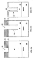
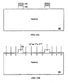
- Fig. 1A illustrates a common method of fabricating a semiconductor device.
- a dopant is introduced in an N or P substrate 100 through an opening formed in a mask layer 102, which could be an oxide, a nitride, photoresist, or some combination thereof.
- the dopant could be introduced by ion implantation or by a high-temperature predeposition (i.e. a shallow diffusion where a source of doping from a gaseous or solid source is introduced into the semiconductor).
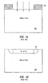
- the dopant may then be diffused by heating to form a shallow region 104 as shown in Fig. 1B , or the dopant may diffused at a higher temperature or for a longer time to form a much deeper region 106, as shown in Fig. 1C .
- Region 104 could be 0.5 to 2 ⁇ m deep and region 106 could be 2 ⁇ m to 10 ⁇ m deep.
- Fig.1D is a view of the left side of region 106, showing in detail the lateral spreading of region 106 during the thermal diffusion process.
- the junction dopant spreads laterally as well as vertically during the diffusion.
- the lateral spreading from the point (0,0) at the edge of the mask opening is equal to about 0.8 times the vertical depth (X j ) of the junction. This lateral spreading of dopant limits the horizontal spacing and packing density of devices formed using a conventional thermal diffusion process.
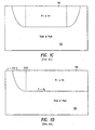
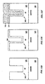
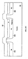
- Figs. 2A and 2B illustrate another problem with diffusion processes, i.e., the depth of the junction can be a function of the width of the mask opening.
- Fig. 2A shows the results of a diffusion performed after an implant through a mask opening W 1
- Fig 2B shows the results of a diffusion performed after an implant through a mask opening W 2 , where W 1 > W 2 .
- the final depth of the junction in Fig. 2B is less than the depth of the junction in Fig. 2A by a factor ⁇ , which is less than one. This phenomenon occurs because the lateral spreading of the dopant when the mask opening is relatively small reduces the surface concentration and the gradient of the doping concentration in a vertical direction more than when the mask opening is large.
- the dopant diffuses downward more slowly when the mask opening is small, an effect referred to as "starved diffusion". Therefore, the mask opening must be relatively large in order get a deep junction, for example, to create a sidewall isolation region for a thick layer. Again, the necessity of a large mask opening limits the packing density of the semiconductor devices.
- Figs. 3A and 3B exemplifies some of the impact of these problems.
- a deep diffusion 108 of the form shown in Fig. 3A is not possible. Instead, the result is a much wider diffusion 112 shown in Fig. 3B , which is separated from diffusion 110 by a much smaller distance Y N+/P+ , despite having the same spacing between the mask features of both N+ and P+ junctions.
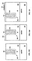
- FIG. 4A shows an ideal structure that includes a vertical P isolation region 114 extending through an N-epi layer 116 to a P substrate 120.
- An N buried layer (NBL) 118 is formed at the interface between N-epi layer 116 and P substrate 120.
- Both P isolation region 114 and N buried layer 118 are sharp, well defined regions with vertical edges, separated by a distance W 3 .
- W 3 a distance
- N buried layer 118 expands horizontally during the growth of N-epi layer 116 and the subsequent driving-in ofP isolation region 114, and P isolation region 114 likewise expands laterally, reducing the separation between N buried layer 118 and P isolation region 114 to a distance W 4 that is much less than W 3 .
- W 4 the breakdown voltage between N buried layer 118 and P isolation region
- Figs. 5A-5F show the steps of a conventional process junction -isolation, i.e., isolation extending downward from the top surface (also known as "down-only" junction isolation.).
- a thick oxide layer 122 e.g., 1 to 5 ⁇ m thick
- a photoresist layer 126 has been formed on top of oxide layer 122 and oxide layer 122 has been etched through an opening in photoresist layer 126.
- a thin oxide layer 130 is formed in the opening and a slow-diffusing N-type dopant such as antimony or arsenic is implanted through the opening to form an N buried layer 128, shown in Fig. 5C .
- N buried layer 128 is driven in at a high temperature for an extended period of time, e.g., 1100 to 1250 °C for 5 to 20 hours. The length and temperature of this thermal process is made necessary by the fact that for purposes of later processing the dopant used to form N buried layer 128 is one that diffuses slowly, so diffusing it away from the silicon surface prior to epitaxy necessarily takes high temperatures and long times.
- Fig. 5D shows the structure after the growth of an N epi layer 132 on P substrate 124. As indicated, N buried layer 128 has diffused upward into N epi layer 132.
- an oxide layer 134 is formed on the surface of N epi layer 132 and an opening is etched in oxide layer 134 using a photoresist mask layer 136.
- a P-type dopant such as boron is implanted through the opening in oxide layer 134 to form P isolation region 136.
- the entire structure is then subjected to a thermal process, which causes P isolation region 136 to diffuse downward through N epi layer 132 to P substrate 124, at the same time forming a thin oxide layer 138.
- N buried layer 128 diffuses upward and laterally during this thermal process.
- N buried layer 128 is formed of a slow-diffusing dopant, it diffuses more slowly than the boron in P isolation region 136, and thus N buried layer 128 remains separated from P isolation region 136. Nonetheless, to guarantee this separation, N epi layer 132 must be made thicker than would otherwise be desirable.
- Fig. 6 illustrates a way of reducing this problem by forming a P buried layer 140 directly below P isolation region 136.
- P buried layer 140 diffuses upward during the thermal process and meets the down-diffusing P isolation region 136 sometime near the middle of N epi layer 132, thereby reducing the amount of thermal processing required and the lateral diffusion ofN buried layer 128. Nonetheless, such lateral diffusion does occur and wafer space is therefore still wasted.
- Figs. 7A-7F illustrate a process for forming the structure of Fig. 6 .
- Fig. 7A shows the structure after N buried layer 128 has been implanted and thermally diffused to reduce the surface dopant concentration before the growth of an epitaxial layer.
- a thick oxide layer 146 is formed.
- the oxide atop the NBL may grow to a slightly greater thickness than those portions growing over the more lightly doped P-type substrate(an effect know as "concentration enhanced oxidation").
- the result may be an oxide layer 142 that has a thickness less than the thickness of oxide 146 despite having the same oxidation time.
- a photoresist layer 144 is deposited on top of oxide layers 142 and 146 and patterned for the implant of boron ions to form P buried layer 140.
- the edge of the opening in photoresist layer 144 is spaced a lateral distance W 5 from the edge of N buried layer 128 to ensure that N buried layer 128 and P buried layer 140 do not merge during subsequent thermal processing.
- oxide layer 142 is etched through the opening in photoresist layer 144, and boron (or another P-type dopant) is implanted through the opening to form P buried layer 140.
- the structure is again annealed to reduce the surface concentration of P buried layer 140, forming a thin oxide layer 148, as shown in Fig. 7C .
- N epi layer 132 is grown on top of P substrate 124 using epitaxial deposition, as shown in Fig. 7D .
- Normally vapor phase epitaxial (VPE) deposition is preferred over liquid phase epitaxy, especially in the deposition of silicon.
- VPE requires the substrate to be heated to a high temperature, typically above 1200 °C.
- N buried layer 128 and P buried layer 140 spread both vertically and laterally, reducing the separation between these two buried layers.
- an oxide layer 150 is formed on the surface ofN epi layer 132.
- Oxide layer 150 is patterned using common photolithographic techniques to form an opening through which boron is implanted to form P isolation region 136.
- the structure is then annealed once again to cause P buried layer 140 to diffuse upward and P isolation region 136 to diffuse downward until these two diffusions merge somewhere within N epi layer 132.
- N buried layer 128 and P buried layer 140 diffuse laterally during this anneal until the separation between them becomes quite small. Absent the separation W 5 shown in Fig. 7A , these two buried layers would in fact merge, and therefore the separation W 5 is in effect the "penalty" that must be paid to assure that in the final structure P buried layer 140 is spaced sufficiently from N buried layer 128 to provide the required breakdown voltage.
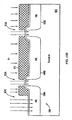
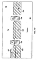
- Fig. 8 shows a way of avoiding this problem by etching a trench 152 all the way through the N epi layer 132 and filling trench 152 with a dielectric 154.
- Trench 152 might have to be very deep to extend entirely through N epi layer 132, since N epi layer could be anywhere from 5 ⁇ m to 20 ⁇ m thick, for example.
- FIG. 9A-9F A process for forming the structure of Fig. 8 is shown in Figs. 9A-9F .
- an oxide or other hard mask layer 156. is deposited on N epi layer 132 and patterned with a photoresist layer 158, as shown in Fig. 9A .
- An opening 160 is thereby formed in layer 156, as shown in Fig. 9B , and trench 152 is etched through N epi layer 132, as shown in Fig. 9C . This is typically done by a reactive ion etch (RIE).
- RIE reactive ion etch
- trench 152 After trench 152 has been formed, hard mask layer 156 is removed, and a sacrificial oxide layer (not shown) is grown in trench 152 to repair crystalline damage caused by the RIE process.
- the sacrificial oxide layer is removed and another oxide layer 162 is grown in the walls of trench 152 and top surface ofN epi layer 132, as shown in Fig. 9D .
- Trench 152 is filled with a dielectric material 164 which overlaps the top surface ofN epi layer 132, as shown in Fig. 9E , and dielectric material 164 is planarized as shown in Fig. 9F , so that the top surface of dielectric material 164 is level with the top surface of oxide layer 162.
- trench 152 Since trench 152 does not expand or spread significantly during this process, and since it does not form a PN junction to the epitaxial layer, trench 152 can be located closer to N buried layer 128 than, for example, P buried layer 140 at the stage shown in Fig. 7C . Nonetheless, this process has several problems and risks. Because trench 152 can be very deep, it may be difficult to fill. As shown in Fig.10A , if trench is under filled, a narrow gap may be left extending downward from the top surface of dielectric material 164 conformal to the trench itself, as shown in Fig. 10A , or a narrow void may be left in the trench, as shown in Fig. 10B .
- a void may be left in the bottom portion, as shown in Fig. 10C , or if the RIE is somewhat less anisotropic producing a trench with a wide mouth, the dielectric 164 may be removed from the inside of the trench during the etchback leaving only a small portion in the bottom of the trench, as shown in Fig. 10D .
- deep trench isolation and re-fill remains a challenging process for high volume manufacturing
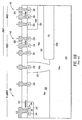
- Figs. 11A-11E illustrate several semiconductor devices formed using prior art diffusion techniques.
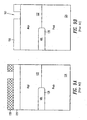
- Fig. 11A shows an NPN transistor 234 and a PNP transistor 236 that are formed in an N epi layer 202 grown on a P substrate 200.
- the emitter of NPN transistor is an N+ region 208
- the base includes a P+ region (the base contact, or extrinsic base) 210 and a dedicated P-base region (the active transistor or intrinsic base regions) 206
- the collector includes an N+ region 212 (collector contact region), a portion of N epi layer 202 (the collector), and an N buried layer 204A (a so-called sub-collector region).
- N buried layer 204A isolates transistor 234 from P substrate 200 and lowers the resistance of the collector.
- the emitter is a P+ region 226, the base includes an N+ extrinsic base contact region 224 and a dedicated intrinsic base region 222, and the collector including a P+ collector contact region 228, a P-well 220, and a P buried layer sub-collector 218.
- PNP transistor 236 is isolated from P substrate 200 by an N buried layer 204B.
- N buried layer (NBL) 204B and P buried layer (PBL) 218 are formed at the interface ofN epi layer 202 and P substrate 200.
- N buried layer 204B may be formed with a relatively slow-diffusing dopant such as antimony or arsenic, and P buried layer 218 may be formed with a fast diffusing dopant such as boron.
- P buried layer 218 extend above N buried layer 204B, and in some cases may extend both above and below the NBL.
- NPN transistor 234 is isolated from PNP transistor 236 by a P isolation region 214, which extends from the surface ofN epi layer 202 into P substrate 200.
- P isolation region 214 also provides a means of setting the potential of P substrate 200 through a P+ contact region 216, and is often biased at the most negative on-chip potential or ground.
- the potential of the portion ofN epi layer 202 in PNP transistor 236 can be set through an N+ contact region 230, where the NBL 204B must be biased at a potential equal to or more positive than P substrate 200 and equal to or more positive than PBL 218.
- Common practice often involves biasing NBL at the positive supply rail (e.g. Vcc) or shorting PBL 218 and NBL 204B to the same potential (a zero biased junction).
- Fig. 11B shows a lateral double-diffused N-channel MOSFET 238 (also known as an LDMOSFET) and an isolated CMOS pair that includes a PMOSFET 240 and an NMOSFET 242.
- the devices are formed in N epi layer 202.
- the channel portion of P-body (or P well) 248 underlies a gate 247, setting the threshold voltage of the MOSFET and preventing punch-through breakdown between the source and the drain (by forcing the majority of the depletion spreading of the P-body to N-epi junction into the epitaxial drain side of the device).
- a gate 247 setting the threshold voltage of the MOSFET and preventing punch-through breakdown between the source and the drain (by forcing the majority of the depletion spreading of the P-body to N-epi junction into the epitaxial drain side of the device.
- the difference injunction depth between the body 248 and the source 246 along the surface i.e. laterally, sets the channel length of the LDMOSFET.
- P-body 248 is implanted after the gate electrode of the device is formed, after which the junction is diffused for a long time and at high temperatures (e.g. 1100 °C for 14 hours) to achieve a sufficient junction depth and channel length. Since both source and body junction are formed after the gate, the device is self aligned.
- P-well diffusion 265 (used in the CMOS) is used as the body of the device. Since the well is formed prior to the gate it is not self-aligned to the gate, making punchthrough and threshold voltage dependent on mask alignment.
- a section of N epi layer 202 that separates the channel from N+ region increases the breakdown potential of the device provided it also is adequately spaced from both the P-body region 248 and spaced from isolation diffusion 250.
- the source is a P+ region 256
- the body includes an N+ contact region 254 and a portion of N epi layer 202
- the drain is a P+ region 258.
- the channel portion of N epi layer 202 underlies a gate 260.
- the source is an N+ region 264
- the body includes a P+ contact region 262 and a P well 265, and the drain is an N+ region 266.
- the channel portion of P well 265 underlies a gate 268.
- the CMOS pair and lightly-doped drain NMOSFET 238 are separated from each other by a P isolation region 250. Contact to P substrate 200 is made through P isolation region 250 and a P+ contact region 252.
- NBL 204 isolates P-well 265 from substrate P substrate 200.
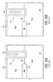
- Fig.11C shows an N-channel quasi-vertical DMOSFET 270, another variant of an N-channel lateral DMOSFET 272, and a fully isolated PMOSFET 274.
- Quasi-vertical DMOSFET 270 is built as a matrix of cells bordered by gates 276A, 276B and 276C.
- Each cell of DMOSFET 270 includes an N+ region 280 that functions as a source, and a P+ region 282 and P-body 278 that together function as a body. The source and body are shorted together.
- DMOSFET 270 is isolated from P substrate 200 by N buried layer 204D, which also lowers the resistance of the device.
- N-channel Lateral DMOSFET 272 includes an N+ region 298 that functions as a source, and a P+ region 294 and P-body 292 that together function as a body. The current flows from N+ region 298, through a channel under a gate 296, down to an N buried layer 204E and along the surface in N epi layer 202, and then up through an N sinker 300 and an N+ region 302 to the drain terminal.
- N-channel LDMOSFET 272 is isolated from P substrate 200 by N buried layer 204E and from DMOSFET 270 by a P isolation region 288 and a P buried layer 290.
- Isolated PMOSFET 274 includes P+ region 310 that functions as the source and a P+ region 312 that functions as the drain.
- the body is a portion ofN epi layer 202 and is contacted by an N+ contact region 308.
- the current flows from P+ region 310 to P+ region 312 through a channel that underlies a gate 314.
- PMOSFET 274 is isolated from P substrate 200 by N buried layer 204F and from NMOSFET 272 by a P isolation region 304 and a P buried layer 306.
- Fig.11D shows another N-channel lateral DMOSFET variant 308, a lateral NMOSFET 310, and a vertical PNP bipolar transistor 312.
- N-channel LDMOSFET 308 is similar to NMOSFET 238 shown in Fig. 11B (similar components are similarly numbered), except that gate 314 steps up over a field oxide layer and lightly-doped NMOSFET 308 is isolated from P substrate 200 by an N buried layer 204G.
- N-channel Lateral DMOSFET 310 is similar to N-channel LDMOSFET 242 shown in Fig.11B , except that NMOSFET 310 does not include N buried layer 204
- a P+ region 314 serves as the emitter
- an N-base 316, an N+ region 318, and a portion of N epi layer 202 serve as the base
- a P buried layer 320 and a P sinker 322 serve as the collector.
- PNP transistor 312 is isolated from P substrate 200 by an N buried layer 204H.
- N-channel lateral DMOSFET 308 is isolated from lateral NMOSFET 310 by a P isolation diffusion 324 and a P buried layer 326, and lateral NMOSFET 310 is isolated from vertical PNP bipolar transistor 312 by a P sinker 328 and a P buried layer 330.
- Fig. 11E shows devices formed in a P epi layer 342 that is grown on a.P substrate 340.
- a CMOS pair includes a PMOSFET 344 and an NMOSFET 346.
- PMOSFET 344 and NMOSFET 346 are similar to PMOSFET 240 and NMOSFET 242 shown in Fig. 11B except that PMOSFET 344 is formed in an N well 350 and NMOSFET 346 is formed in P epi layer 342.
- PMOSFET 344 and NMOSFET 346 are isolated from P substrate 340 by an isolation structure that includes an N buried layer 356 and N isolation diffusions (NI) 352 and 354.
- the bias of the isolation structure can be set via an N+ region 358 and is often biased at the most positive supply voltage that power the CMOS devices.
- An N-channel lightly-doped lateral DMOSFET 348 includes an N+ region 360 as the source, a P+ region 364, a.P-body 362 and a portion ofP epi layer 342 as the body, and an N- lightly doped drain region 366, and N well 368 and an N+ region 370 as the drain.
- a channel is formed in P well 362 and P epi layer 342 under a gate 372.
- NMOSFET 348 is not isolated from P substrate 340.
- a common feature of the devices shown in Figs. 11A-11E is that they generally require lengthy thermal diffusions in order to make connections through the epi layer. These connections may be required to form isolation regions or to connect to buried layers which function as integral components of the devices. Providing high breakdown voltages generally requires a thicker epi layer and more lengthy thermal processes. The thermal processes all produce lateral as well as vertical dopant spreading, both in the isolation regions that are implanted from above and the buried layers that up-diffuse from below. This lateral dopant spreading limits the spacing and packing density that is achievable with these prior art processes.
- US 5 410 175 A relates to a monolithic IC having a PIN photodiode and an n-p-n bipolar transistor formed on a single semiconductor (silicon) substrate.
- a monolithic IC having a PIN photodiode and an n-p-n bipolar transistor formed on a single semiconductor (silicon) substrate.
- the surface of the substrate flat According to this invention, the inter-device isolation between the above-described two devices is attained by forming two epitaxial layers on the silicon substrate, forming trenches in the layers, and burying silicon dioxide in the trenches.
- wiring capacity is small, and high-speed performance becomes possible.
- a p-type buried-layer is formed below the bipolar transistor to thereby prevent punch through between the bipolar transistor and other devices.; Also this invention provides the process for fabricating a planar type bipolar transistor suitable to fabricate the monolithic IC and also provides a PIN photodiode of a new structure.
- EP 0589675 A2 a process is disclosed which simultaneously forms high quality complementary bipolar transistors, relatively high voltage CMOS transistors, relatively low voltage CMOS transistors, DMOS transistors, zener diodes and thin-film resistors, or any desired combination of these, all on the same integrated circuit chip.
- the process uses a small number of masking steps, forms high performance transistor structures, and results in a high yield of functioning die. Isolation structures, bipolar transistor structures, CMOS transistor structures, DMOS transistor structures, zener diode structures, and thin-film resistor structures are also disclosed.
- the JP 63166268 A is directed to stabilize dielectric strength of a semiconductor device, by forming deep P+ type regions reaching an N+ type buried layer so that the P+ type regions provide a part of the base region of an NPN transistor to be formed in an island region of an epitaxial layer on a P-type substrate having the N+ type buried layer, or provide emitter and collector regions of a lateral PNP transistor.
- An N+ type buried layer and a P+ type buried layer are formed in a P-type silicon substrate and an N- type epitaxial layer is deposited thereon. In the wafer thus constructed, a P+ isolation region is formed by diffusion so deep as to reach the P+ type buried layer.
- a P+ type region is formed by diffusion in an island region for an NPN transistor while P+ type regions are formed in an island region for a lateral PNP transistor such that they all reach the N+ type buried layer.
- a P-type region is then formed by diffusion such that it is joined with the P+ type region.
- an N+ type region for a collector electrode is formed by diffusion in the island region and an N+ type region for an emitter region is formed in the P region.
- N+ type region for a base electrode is formed by diffusion in the island region. Accordingly, the semiconductor device is allowed to have increased and stable dielectric strength without increasing sizes of elements
- US 6,352,901 B1 discloses a process for fabricating a bipolar junction transistor, featuring the use of multiple self-aligned collector regions, used to limit the width of the base region of the transistor .
- the self-aligned collector regions are formed via multiple ion implantation procedures, performed through, and self-aligned to, an overlying emitter opening, in an oxide layer.
- the self-aligned collector regions completely fill the space in the lighter doped collector region, located between the overlying base region, and the underlying subcollector region.
- US 6,420,771 B2 discloses a bipolar transistor which is vertically isolated from underlying silicon by an isolation layer of conductivity type opposite that of the collector.
- This isolation layer lies beneath the heavily doped buried layer portion of the collector, and is formed either by ion implantation prior to epitaxial growth of well regions, or by high energy ion implantation into the substrate prior to formation of the well and the heavily doped buried collector layer. Utilization of trench lateral isolation extending into the semiconductor material beyond the isolation layer permits blanket implant of the isolation layer, obviating the need for an additional masking step.
- the lateral spreading of dopant during a thermal diffusion process is constrained by forming a trench on one or several sides of a diffusion (prior to the diffusion) and filling the trench with an oxide or other dielectric material.
- the lateral spreading of the dopant is constrained in several directions by forming trenches on two or more sides of the dopant, especially on the more deeply diffused junctions in a process.
- the trenches constraining diffusions have a sufficient depth that the mostly highly-doped surface portion of the diffusion is constrained by the trench, the trench having a depth preferably at least 15 to 20% of the final depth of the junction. In some cases the trench constrains diffusion in its entirety, i.e. the trench being deeper than the final junction depth. In one preferred embodiment, the trenches are of sufficient depth to constrain the more highly doped-portion of a diffusion and sufficiently shallow to easily fill and planarize.
- the trench extends into the epitaxial layer but does not extend through the epitaxial layer and into the underlying substrate.
- devices are isolated by deep junction isolations where a substantial portion of the isolating junctions are constrained by dielectric-filled trenches.
- an updiffusing buried layer overlaps the trench-constrained down-diffusing diffusion to complete the isolation structure.
- This process is particularly useful in constructing relatively high-voltage devices in an epitaxial layer.
- Bipolar transistor devices rated for reliable operation at a 20V operating voltage, for example, which would typically require a breakdown voltage in the range of 60V to 70V.
- This requires a relatively thick epitaxial layer and deep diffusions extending through the epitaxial layer to isolate the devices electrically from the substrate or from each other. The isolation is provided by a reverse-biased PN junction.
- these deep diffusions require a substantial thermal budget (a product of temperature and time), which also causes the diffusions to spread laterally and increases the size of the devices, limiting the number of devices that can be placed in a given area of the wafer.
- the lateral expansion of the diffusion is limited because the diffusivity of the dopant in the dielectric material in the trench is typically less than the diffusivity of the dopant in the semiconductor substrate or epitaxial layer. Furthermore the dopant after having diffused into the dielectric of the trench, is not electrically active and does not affect or influence the junction breakdown of neighboring junctions or devices. Moreover, even if dopants of opposite conductivity do come into contact with each other in the region below the trench, typically the doping concentration of the diffusion in this locale is sufficiently low that the breakdown voltage of the PN junction is relatively high. Thus, use of this invention allows a higher packing density and provides a far more efficient use of the available space on the wafer. For example, devices may be spaced only one micron apart instead of tens of microns.
- the dielectric-filled trench may extend from the surface of an epitaxial layer or substrate into a submerged region.
- the submerged region can be either a buried layer formed at the interface between an epitaxial layer and a substrate or a deep region formed by implanting dopant at a relatively high energy into a substrate.
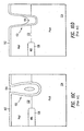
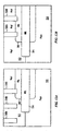
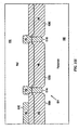
- Figs. 12A and 12B show a structure that includes an N buried layer 514 and a P buried layer 516 formed at an interface between a P substrate 510 and an N epi layer 512.
- P buried layer 516 has diffused upward beyond the upper edge of N buried layer 514. This, in combination with the fact that N buried layer 514 extends laterally beyond P buried layer 516, produces a portion of P buried layer 516 that is above N buried layer 514 and is isolated from P substrate 510.
- the trenches may also be used to form trench-constrained diffusions, either as sinkers, isolation, or wells.
- N epi layer 512 can be divided into isolated pockets by dielectric-filled trenches that extend downward from the surface of N epi layer 512.
- a dielectric-filled trench 518C divides N epi layer 512 into isolated pockets.
- each of dielectric-filled trenches 520A and 520B divides N epi layer 512 into isolated pockets.
- the dielectric-filled trenches should extend into P buried layer 516, but in order to permit current to flow laterally throughout P buried layer 516 the trenches should not extend through P buried layer 516 and into N buried layer 514.
- the trenches may also be used to form trench-constrained diffusions, either as sinkers, isolation, or wells.
- Deep trench isolation uses a trench that completely cuts through the epitaxial layer and into the underlying substrate. Therefore in a DTI process, in any cross section where the trench is present, lateral current flow (in wells, diffused junctions and even buried layers) is cut off, i.e. interrupted by the presence of the trench. For example when it is desirable to completely isolate unrelated devices from one another, like the collectors of two adjacent bipolar devices, the depth of a DTI-type trench is useful.
- N buried layer 514 may also be made anywhere along a device's lateral extent, including the edge, and N buried layer 514 will still be biased to a common potential, allowing lateral current flow (parallel to the wafer's s surface) in NBL 514. If a DTI trench were used, the N buried layer would be cut into separate islands, each one requiring its own electrical contact.
- Figs.13A-13I illustrate a possible process for forming a dielectric-filled trench.
- the trench is shown as being formed in an epi layer that is grown on a substrate.
- the epi layer and substrate could be of the same electrical conductivity type (either N or P) or of different conductivity types.
- the trench may be formed in a substrate without an epitaxial layer. The process would remain essentially the same in those conditions except the criteria for trench depth may differ.
- a hard mask layer 534 of a material such as an oxide or nitride (or a sandwich thereof) is formed on the surface of epi layer 532.
- Hard mask layer 534 is masked with a photoresist layer 536, and etched to form an opening 358.
- a trench 540 is etched, typically using a reactive ion etch (RIE).
- RIE reactive ion etch
- photoresist layer 536 While in processes for producing trench-gated MOSFETs photoresist layer 536 is often removed before the RIE, here it may be desirable to leave photoresist layer 536 in place during the RIE, since the trench may be deeper (e.g., 2-4 ⁇ m deep) than the trenches commonly used for trench gated vertical power MOSFETs. Alternatively, the thickness of the hard mask layer 534 can be increased to survive the silicon trench etching process.
- Hard mask layer 534 and photoresist layer 536 are removed (or with a mask selectively removed) and, optionally, a sacrificial oxide layer 542 is formed on the walls of trench 540, as shown in Fig. 13C , and removed, as shown in Fig. 13D .
- a sacrificial oxide layer 542 is formed on the walls of trench 540, as shown in Fig. 13C , and removed, as shown in Fig. 13D .
- An oxide liner 544 is grown on the walls of trench 540, as shown in Fig.13E , and a dielectric 546 such as a TEOS oxide is deposited in trench 540 and over the surface of epi layer 532, as shown in Fig. 13F .
- Oxide liner 544 acts as a shield against dopants, such as boron and/or phosphorus, that may be included in dielectric 546 to make dielectric 546 flow and fill into trench 540 more readily.
- dopants such as boron and/or phosphorus
- the electrical characteristics of the devices could be altered if such dopants were allowed enter epi layer 532. In some cases it may be possible to omit the oxide liner, possibly by first depositing an undoped oxide into the trench.
- the top surface of the structure can be planarized by chemical-mechanical polishing (CMP) to form a semi-flat surface as shown in Fig. 13G .
- CMP chemical-mechanical polishing
- the surface of epi layer 532 is re-oxidized to form an oxide layer 548, as shown in Fig. 13H . Since the oxidation process consumes part of epi layer 532 but not the oxide 546 (which is already oxidized), an indentation is produced over trench 540. Alternatively, a portion of oxide liner 544 may be left on the top surface of epi layer 532 in the planarization process, in which case the re-oxidation step shown in Fig. 13H may be unnecessary.
- etchback of the glass 546 in Fig. 13F which will not produce as planar a surface as shown in Fig. 13G .
- Some indentation over the trench is likely since deposited oxides tend to etch faster.
- a silicon nitride may be deposited and planarized using CMP methods to cap or seal the top of the trench with nitride.
- a polysilicon layer 550 can be deposited and patterned on oxide layer 548 for use in forming a resistor or capacitor. If a capacitor is to be formed between polysilicon layer 550 and epi layer 532, the thickness of oxide layer 548 is critical and it may be desirable to grow oxide layer 548 by thermal means rather than depositing oxide layer 548, since thermal processes generally provide greater control over the thickness of an oxide layer than deposition processes. This factor is not important if polysilicon layer 550 is to be used either as a resistor or as a capacitor with another, overlying polysilicon layer.
- Figs. 12 and 13 are building blocks that can be used in the fabrication of a wide variety of semiconductor devices, including but not limited to bipolar transistors, MOSFETs, diodes, and the like. These process steps include integration of structures using trench constrained diffusions and junctions.
- Figs. 14 and 15 illustrate the use of trench-constrained diffusion in the construction of complementary (i.e. integration of both NPN and PNP) analog bipolar transistors .
- the term "analog" is included only to identify that the purpose of the technology is to produce bipolar devices capable of making high quality current sources (high Early voltage devices) and high breakdown voltages, e.g. greater than 3 or 5V without suffering the problem of BVceo snapback to a sustaining voltage lower than the supply voltage.
- the trench constrained diffusion techniques are not limited to the fabrication of analog bipolars, and may be used for digitally optimized bipolars as well.
- Fig. 14 provides a general overview of the process.
- Each of the "cards" represents a process step.
- the cards with clipped corners denote steps that are optional, although other steps may also be omitted in particular situations.
- the process starts with a series of implants and diffusions into the substrate and the growth of an epitaxial layer on the substrate.
- Next steps relating to the construction of medium-depth partial trench isolation (PTI) regions are performed. Deep junctions are implanted and diffused ideally using layouts benefiting from trench constrained diffusion, and the base regions of the bipolar transistors are formed.
- a polysilicon capacitor may be constructed. Then come the "late” implants, which form the emitter and collector regions of the transistors.
- a double layer metal (DLM) interconnect structure is built above the silicon for providing connections to the regions in the silicon.
- the so-called “+5 process” refers to the entire DLM interconnect sequence using 5 masks, one to define and etch the contact to the silicon, another for metal 1, a third for the via etch of interlayer dielectric between metal 1 and metal 2, a fourth mask for metal 2, and lastly a mask to etch the passivation layer for bonding pads.
- a "+3 process” produces single layer metal (SLM)
- the so-called “+5 process” results in dual layer metal (DLM)
- a "+7 process” results in triple layer metal interconnects. All of these interconnect options are compatible with the process flow as shown, and are mutually compatible with the use of trench constrained junctions and diffusions.
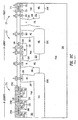
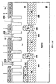
- an oxide layer 602 and a photoresist layer 604 are deposited in succession on a P substrate 600, and photoresist layer 604 is patterned and oxide layer 602 is etched through openings in the photoresist layer 604. Photoresist layer 604 is removed, and antimony and single- or double-ionized phosphorus (or a combination of both) are implanted (using conditions comparable to those described above) through the openings in oxide layer 602, as shown in Fig. 15B .
- Oxide layer 602 is removed, and the antimony and phosphorus are driven-in for an extended period of time. This causes a new oxide layer 606 to form on the surface of P substrate 600, and an N buried layer 608, broken into sections 608A, 608B and 608C, is formed below the surface of P substrate 600. Sections 608A, 608B and 608C are separated at the locations where oxide layer 602 remained after oxide layer 602 was etched through the openings in photoresist layer 604.
- oxide layer 606 is removed, and a photoresist layer 610 is deposited and patterned. Openings 612A and 612B are formed in photoresist layer 610 above gaps separating sections 608A, 608B and 608C of N buried layer 608 and an opening 612C is formed in photoresist layer 610 above section 608A ofN buried layer 608. Boron is implanted through openings 612A, 612B and 612C to form sections 614A and 614B of a P buried layer 614 in P substrate 600 (see Fig. 15E ).
- the dose of the boron implant should be fairly high (e.g., 3E14 to 7E15 cm -2 ) to ensure that the boron overcomes the phosphorus doping in the overlap regions. If only a slow-diffusing dopant such as antimony or arsenic were used to form N buried layer 608, the dose of the boron implant could be reduced possibly to a dose as low as 8E 13 cm -2 .
- the boron dopant that passes through opening 612C does not counterdope the phosphorus and antimony in N buried layer section 608A and thus is not shown in Fig. 15E .
- an N epitaxial (epi) layer 616 is grown on top of P substrate 600.
- N buried layer 608 and P buried layer 614 diffuse upwards into N epi layer 616. No additional diffusion is required to form this junction since the epitaxial deposition process itself occurs at a high temperature. Since N buried layer 608 includes the fast-diffusing dopant phosphorus, the peak dopant concentration in N buried layer 608 moves substantially downward during the drive-in of the phosphorus and antimony implants in the diffusion performed prior to the epitaxial growth.
- the boron generally moves ahead of the phosphorus (the boron having both a higher concentration and a higher diffusivity), and P buried layer 614 reaches higher into N epi layer 616 than the phosphorus and antimony dopants of N buried layer 614. Conversely, as shown in Fig. 15E , P buried layer 614 does not extend below the phosphorus/antimony diffusions in P substrate 600.
- Sections 614A and 614B of P buried layer 618 may touch sections 608A, 608B and 608C of N buried layer 608, as shown in Fig. 15E , or sections 614A and 614B of P buried layer 618 may be separated from sections 608A, 608B and 608C ofN buried layer 608, as shown in Fig. 15F .
- the spacing, or lack thereof, between sections 614A and 614B of P buried layer 618 and sections 608A, 608B and 608C of N buried layer 608 is controlled by varying the width of openings 612A and 612B in photoresist layer 610 (see Fig. 15D ). In the remainder of this discussion it will be assumed that the width of openings 612A and 612B was set so as to yield the embodiment shown in Fig. 15F .
- trenches 618 are formed in N epi layer 616 and filled with an oxide layer 622, preferably using the process shown in Figs. 13A-13I .
- Trenches 618 form intervening mesas 620A-6201 in N epi layer 616.
- trenches 618 do not extend as deep as the upper boundary of P buried layer 614.
- the trenches could extend into P buried layer 614, but they should not extend entirely through P buried layer 614 or entirely through N epi layer 616 into the P substrate 600.
- Trenches 618 are preferably in the range of 0.8 to 1.2 ⁇ m wide although more narrow trenches may be used.
- trenches 618 are aligned to the vertical edge of sections 614A, 614B and 614C of P buried layer 614.
- trench 618B is aligned to an edge of section 614A
- trenches 618C and 618D are aligned to the opposite edges of section 614B
- trenches 618F and 618G are aligned to the opposite edges of section 614C. Consequently, mesa 620B is above section 614C, mesa 620D is above section 614A, and mesa 620G is above section 614B.
- Fig. 15C shows edges formed in P substrate 600 during the formation of N buried layer 608 prior to epi growth. These edges, while covered by silicon during the growth of N epi layer 616, still can be seen at the bottom edge of the epi, at the substrate-epi interface, by infrared light.
- the techniques employed in aligning features on the surface of an epi layer to buried layers are well known to those skilled in the art and thus will not be described in further detail here.
- trench 618 as shown in Fig 29G is illustrated to be roughly half the thickness of epi layer 616, but in examples not forming part of the claimed invention it may extend deeper of be made more shallow according to the process requirements. Most importantly, it does not extend completely through the epitaxial layer, i.e. the trench is not as deep as the epitaxy is thick, and so it should not be considered as deep trench isolation or an equivalent thereof.
- the trench at the time it is etched and filled has a depth that nearly overlaps onto but in fact is spaced from P buried layer 614C. Later in subsequent thermal processing the PBL 614C layer will updiffuse and may overlap with trench 618, although that outcome is not mandated by the process flow.
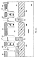
- a photoresist layer 624 is formed on the surface of oxide layer 622 and patterned with openings over mesas 620C, 620F and 620H.
- Arsenic and phosphorus are implanted through the openings in photoresist layer 624 to form N+ sinkers 626C, 626F and 626H in mesas 620C, 620F and 620H, respectively, as shown in Fig. 14I.
- the phosphorus diffuses rapidly and the arsenic diffuses more slowly and thus the combination of these two dopants levels out the dopant profile ofN+ sinkers 626C, 626F and 626H.
- the hybrid implant comprising both arsenic and phosphorus involves two dopant with substantially different diffusivities.
- the faster phosphorus may be more lightly doped than the arsenic (e.g. at 7E13 cm -2 instead of 2E15 cm -2 ) so that the phosphorus doesn't extend too deeply into the silicon during the subsequent thermal processing.
- Photoresist layer 624 is then stripped, and the N-type sinker diffusant may be partially diffused using a high temperature diffusion process at 1000°C to 1200 °C but preferably at between 1100 °C and 1150 °C for 1 to 7 hours. Alternatively, the diffusion can be skipped altogether, or the implant and anneal replaced by a predeposition of phosphorus (using a gaseous source such as POCL 3 ). Predeposition is known in the art and will not be further elaborated upon herein.
- a photoresist layer 628 is formed on the surface of oxide layer 622 and patterned with openings over mesas 620B, 620D, 620G and 620I. Boron is implanted through the openings in photoresist layer 628 to form P+ regions 630B, 630D, 630G and 630I/630I' in mesas 620B, 620D, 620G and 620I, respectively. Photoresist layer 628 is removed.
- the structure is now annealed to drive in the N+ and P+ dopants (herein referred to as the isolation diffusion).
- P+ sinker 630B merges with P buried layer 614C
- N+ sinker 626C merges with N buried layer 608A
- P+ isolation region 630D merges with P buried layer 614A
- N+ sinker 626F merges with N buried layer 608B
- P+ isolation region 630G merges with P buried layer 614B
- N+ sinker 626H merges with N buried layer 608C.
- P+ regions 630I and 630I' diffuse downward but do not merge with any other regions.
- the combination of P+ isolation region 630D and P buried layer 614A and the combination of P+ isolation region 630G and P buried layer 614B form columns of P-type dopant, laterally constrained at the top by trenches 618, the columns extending into P substrate 600 and isolating the devices formed in N epi layer 616 from each other.
- the resulting structure is shown in Fig. 15 J (except that the PB region 638 and NB region 632 has not yet been formed).
- the order of the boron sinkers and isolation, the phosphorus sinkers and the various drive-in diffusions may be changed without substantially changing the resulting device (so long as the total thermal budget, temperature-time cycle, up to this point remains fixed)
- the boron sinkers and isolation can precede the N sinker implants which may (or may not) employ a post implant partial drive diffusion.
- Another alternative is to implant the isolation or the sinker or both using high energy ion implantation with implants up to 3 MeV (but preferably with several implants of differing energy from 0.5 MeV up to 2 MeV), whereby the deeper junction after implantation (already more than 2.5 ⁇ m) requires less diffusion time and temperature than the low-implant energy deep-diffused version of the same.
- Fig. 15 J the N-type diffusions (N sinkers and N buried layers) are shown as spaced from the P-type diffusions (P sinkers and isolation regions and P buried layers). Even if there were contact between the N-type diffusions and P-type diffusions (as in the embodiment shown in Fig. 15E ), this contact could only take place below trenches 618, where the doping concentrations are relatively low. The breakdown voltage of any PN junctions formed in this way would be relatively high, especially compared to the surface junction that would be formed if the trench were not there. In other words, the N sinkers and P isolation regions are separated by trenches 618 near the surface of N epi layer 616, where the doping concentrations of these diffusions are high enough to create low breakdown voltages.
- the doping concentrations of these diffusions are relatively low (and more graded or diffuse) and hence the breakdown voltages across any PN junctions that might be formed would be relatively high.
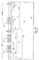
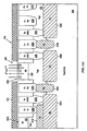
- N epi layer 616 is masked (not shown) and an N-type dopant such as phosphorus is implanted through an opening in the mask to form an N base region 632, shown in Fig. 15 J.
- the phosphorus implant can range from 60 keV to as high as 2 MeV.
- the lower range of implant energies typically requires either a drive-in diffusion later in the process (for a final junction depth of 0.5 ⁇ m to 2.5 ⁇ m), or the use of a polysilicon emitter (for a junction depth under 0.5 ⁇ m). Higher energy implants require little or no diffusion.
- Implant doses range from 3E13 cm -2 to 2E14 cm -2 .
- the photoresist mask is stripped and photoresist layer 634 is deposited and patterned to form an opening 636.
- Boron (B + and/or B ++ ) is implanted through opening 636 to form a P base region 638 in mesa 620E.
- the deeper implant of boron, referred to as the intrinsic base may range in dose from 3E13 cm -2 to 2E14 cm -2 with implant energies ranging from 90 keV to 2 MeV.
- the lower range of implant energies typically requires either a drive-in diffusion later in the process (for a final junction depth of 0.5 ⁇ m to 2.5 ⁇ m), or the use of a polysilicon emitter (for a junction depth under 0.5 ⁇ m). Higher energy implants require little or no diffusion.
- Intrinsic implant doses range from 3E13 cm -2 to 2E14 cm -2 .
- P base region 638 is preferably formed by the superposition of two implants, a low energy implant that creates a low resistance area near the surface ofN epi layer 616 (called an extrinsic base implant) and a higher energy implant that penetrates deeper into N epi layer 616 (the aforementioned intrinsic base implant).
- the extrinsic base implant is typically a B + or BF 2 + species performed at an energy of 30 to 60 keV with a dose greater than 5E14 cm -2 .
- the use of the extrinsic implant has limited use if appreciable base diffusion is performed. For shallow junction devices, it greatly enhances performance.
- the hot time must be removed from the sinker and isolation diffusions.
- photoresist layer 634 is removed and a photoresist layer 640 is deposited and patterned to form a series of openings, as shown in Fig. 15K
- Arsenic is implanted through the openings in photoresist layer 640 to form contact regions in N base 632 and in N sinkers 626C, 626F and 626H and to form an N emitter region 642 in P base region 638.
- N emitter region 642 extends below the heavily doped surface region of P base region 638 (indicated by the dashed line) so that the electrical characteristics of the base are determined by the more lightly doped portion below N emitter region 642, conducting vertically through the intrinsic base.
- the N+ implants may be phosphorus at 30 keV to 50 keV, or preferably arsenic at 60 keV to 120 keV, at a dose of 2E15 cm -2 to 7E15 cm -2 .
- Photoresist layer 640 is removed and a photoresist layer 644 is deposited and patterned to form a series of openings, as shown in Fig. 15L .
- Boron is implanted through the openings in photoresist layer 644 to form contact regions in P regions 630B, 630D, 630G, 630I and 630I', to form a P emitter region 646 in N base region 632, and to form a contact region 648 in P base region 638.
- the P+ implants may be boron at 30 keV to 50 keV, or preferably BF 2 + at 60 keV to 120 keV, at a dose of 2E15 cm -2 to 7E15 cm -2 .
- Photoresist layer 644 is then removed.
- a dielectric layer 650 is deposited on oxide layer 622.
- Dielectric layer 650 is masked, and electric layer 650 and oxide layer 622 are etched through openings in the mask to form openings to the various regions in N epi layer 616.
- a Ti or TiN barrier layer 651 is deposited in the openings, and a first metal layer 652 is deposited over barrier layer 651 and patterned to form metal contacts.
- a second dielectric layer 654 is deposited on dielectric layer 650, and a via mask is applied with openings positioned to make contact to P regions 630B, 630D and 630I. Vias are etched in dielectric layer 654 through the openings in the via mask, and a second metal layer 656 is deposited in the vias.
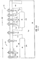
- Vertical PNP transistor 660 includes the following regions: Emitter: P+ region 646 Base: N base region 632 and a portion of N epi layer 616 Collector: P buried layer 614C and P sinker 630B
- Vertical PNP transistor 660 is isolated from P substrate 600 by an isolation structure that includes N buried layer 608A and N sinker 626C.
- Vertical NPN transistor 662 includes the following regions:
- N+ region 642 Base: P base region 638
- Lateral PNP transistor 664 includes the following regions:
- P region 630I' Base A portion ofN epi layer 616, N buried layer 608C, N sinker 626H
- Collector P region 630I
- vertical PNP transistor 660 is isolated from vertical NPN transistor 662 by a vertical column that includes P isolation region 630D and P buried layer 614A.
- Vertical NPN transistor 662 is isolated from lateral PNP transistor 664 by a vertical column that includes P isolation region 630G and P buried layer 614B.
- transistors 660, 662 and 664 would typically have to be spaced from each other by tens of microns because of lateral dopant-spreading during the thermal processes.
- the spacing between transistors 660 662 and 664 shown as X 1 and X 2 in Fig. 15M , can be reduced to only 3 to 4 microns. This allows a large increase in the packing density of the devices on the wafer without sacrificing the quality of the electrical isolation among the devices.
Abstract
Description
- This invention relates to a bipolar transistor arrangement comprising an isolation structure for junction-isolated integrated semiconductor devices, and in particular complementary analog bipolar (CAB) transistors.
- As the minimum feature sizes in integrated circuits become smaller, it becomes necessary to increase the packing density of the devices on the integrated circuit (IC) chip. The benefits of smaller devices are largely forfeited if the distance between devices cannot also be decreased.
-
Figs. 1-11 illustrate prior art processes and structures and some of the problems that are inherent in those processes and structures. -
Fig. 1A illustrates a common method of fabricating a semiconductor device. A dopant is introduced in an N orP substrate 100 through an opening formed in amask layer 102, which could be an oxide, a nitride, photoresist, or some combination thereof. The dopant could be introduced by ion implantation or by a high-temperature predeposition (i.e. a shallow diffusion where a source of doping from a gaseous or solid source is introduced into the semiconductor). The dopant may then be diffused by heating to form ashallow region 104 as shown inFig. 1B , or the dopant may diffused at a higher temperature or for a longer time to form a muchdeeper region 106, as shown inFig. 1C .Region 104 could be 0.5 to 2 µm deep andregion 106 could be 2 µm to 10 µm deep.Fig.1D is a view of the left side ofregion 106, showing in detail the lateral spreading ofregion 106 during the thermal diffusion process. As indicted, the junction dopant spreads laterally as well as vertically during the diffusion. As a general rule, the lateral spreading from the point (0,0) at the edge of the mask opening is equal to about 0.8 times the vertical depth (Xj) of the junction. This lateral spreading of dopant limits the horizontal spacing and packing density of devices formed using a conventional thermal diffusion process. -
Figs. 2A and 2B illustrate another problem with diffusion processes, i.e., the depth of the junction can be a function of the width of the mask opening.Fig. 2A shows the results of a diffusion performed after an implant through a mask opening W1, andFig 2B shows the results of a diffusion performed after an implant through a mask opening W2, where W1 > W2. The final depth of the junction inFig. 2B is less than the depth of the junction inFig. 2A by a factor η, which is less than one. This phenomenon occurs because the lateral spreading of the dopant when the mask opening is relatively small reduces the surface concentration and the gradient of the doping concentration in a vertical direction more than when the mask opening is large. Thus the dopant diffuses downward more slowly when the mask opening is small, an effect referred to as "starved diffusion". Therefore, the mask opening must be relatively large in order get a deep junction, for example, to create a sidewall isolation region for a thick layer. Again, the necessity of a large mask opening limits the packing density of the semiconductor devices. -
Figs. 3A and 3B exemplifies some of the impact of these problems. Ideally, one would like to form adeep diffusion 108 separated from ashallow diffusion 110 by a distance YN+/P+, as shown inFig. 3A . In reality, because of lateral dopant spreading, adeep diffusion 108 of the form shown inFig. 3A is not possible. Instead, the result is a muchwider diffusion 112 shown inFig. 3B , which is separated fromdiffusion 110 by a much smaller distance YN+/P+, despite having the same spacing between the mask features of both N+ and P+ junctions. - A similar problem occurs in the formation of vertical isolation regions and buried layers.
Fig. 4A shows an ideal structure that includes a verticalP isolation region 114 extending through an N-epi layer 116 to aP substrate 120. An N buried layer (NBL) 118 is formed at the interface between N-epi layer 116 andP substrate 120. BothP isolation region 114 and N buried layer 118 are sharp, well defined regions with vertical edges, separated by a distance W3. In reality, what happens with a conventional diffusion process is shown inFig. 4B . N buried layer 118 expands horizontally during the growth of N-epi layer 116 and the subsequent driving-inofP isolation region 114, andP isolation region 114 likewise expands laterally, reducing the separation between N buried layer 118 andP isolation region 114 to a distance W4 that is much less than W3. As a result the breakdown voltage between N buried layer 118 and P isolation region would be reduced and to obtain the breakdown voltage of the structure shown inFig. 4A , one would have to significantly widen the separation between N buried layer 118 andP isolation region 114. -
Figs. 5A-5F show the steps of a conventional process junction -isolation, i.e., isolation extending downward from the top surface (also known as "down-only" junction isolation.). InFig. 5A , a thick oxide layer 122 (e.g., 1 to 5 µm thick) has been grown on aP substrate 124. InFig. 5B , aphotoresist layer 126 has been formed on top ofoxide layer 122 andoxide layer 122 has been etched through an opening inphotoresist layer 126. Athin oxide layer 130 is formed in the opening and a slow-diffusing N-type dopant such as antimony or arsenic is implanted through the opening to form an N buriedlayer 128, shown inFig. 5C . - To prepare for the subsequent growth of an overlying epitaxial layer, the surface concentration of dopant in N buried
layer 128 must be reduced. This is necessary to reduce the outgasing of dopant into the epitaxial reactor during the growth of the epi layer. To accomplish this, N buriedlayer 128 is driven in at a high temperature for an extended period of time, e.g., 1100 to 1250 °C for 5 to 20 hours. The length and temperature of this thermal process is made necessary by the fact that for purposes of later processing the dopant used to form N buriedlayer 128 is one that diffuses slowly, so diffusing it away from the silicon surface prior to epitaxy necessarily takes high temperatures and long times. -
Fig. 5D shows the structure after the growth of anN epi layer 132 onP substrate 124. As indicated, N buriedlayer 128 has diffused upward intoN epi layer 132. - As shown in
Fig. 5E , anoxide layer 134 is formed on the surface ofN epi layer 132 and an opening is etched inoxide layer 134 using aphotoresist mask layer 136. A P-type dopant such as boron is implanted through the opening inoxide layer 134 to formP isolation region 136. The entire structure is then subjected to a thermal process, which causesP isolation region 136 to diffuse downward throughN epi layer 132 toP substrate 124, at the same time forming athin oxide layer 138. N buriedlayer 128 diffuses upward and laterally during this thermal process. Since N buriedlayer 128 is formed of a slow-diffusing dopant, it diffuses more slowly than the boron inP isolation region 136, and thus N buriedlayer 128 remains separated fromP isolation region 136. Nonetheless, to guarantee this separation,N epi layer 132 must be made thicker than would otherwise be desirable. -
Fig. 6 illustrates a way of reducing this problem by forming a P buriedlayer 140 directly belowP isolation region 136. P buriedlayer 140 diffuses upward during the thermal process and meets the down-diffusingP isolation region 136 sometime near the middle ofN epi layer 132, thereby reducing the amount of thermal processing required and the lateral diffusion ofN buriedlayer 128. Nonetheless, such lateral diffusion does occur and wafer space is therefore still wasted. -
Figs. 7A-7F illustrate a process for forming the structure ofFig. 6 .Fig. 7A shows the structure after N buriedlayer 128 has been implanted and thermally diffused to reduce the surface dopant concentration before the growth of an epitaxial layer. During the thermal diffusion process athick oxide layer 146 is formed. In the event that a high concentration of arsenic is used to form the buried layer, the oxide atop the NBL may grow to a slightly greater thickness than those portions growing over the more lightly doped P-type substrate(an effect know as "concentration enhanced oxidation"). The result may be anoxide layer 142 that has a thickness less than the thickness ofoxide 146 despite having the same oxidation time. The phenomena may also occur using antimony as the dopant species, but with a reduced magnitude effect. Aphotoresist layer 144 is deposited on top ofoxide layers layer 140. The edge of the opening inphotoresist layer 144 is spaced a lateral distance W5 from the edge of N buriedlayer 128 to ensure that N buriedlayer 128 and P buriedlayer 140 do not merge during subsequent thermal processing. - As shown in
Fig. 7B ,oxide layer 142 is etched through the opening inphotoresist layer 144, and boron (or another P-type dopant) is implanted through the opening to form P buriedlayer 140. The structure is again annealed to reduce the surface concentration of P buriedlayer 140, forming athin oxide layer 148, as shown inFig. 7C . - Next
N epi layer 132 is grown on top ofP substrate 124 using epitaxial deposition, as shown inFig. 7D . Normally vapor phase epitaxial (VPE) deposition is preferred over liquid phase epitaxy, especially in the deposition of silicon. VPE, however, requires the substrate to be heated to a high temperature, typically above 1200 °C. During the growthofN epi layer 132, N buriedlayer 128 and P buriedlayer 140 spread both vertically and laterally, reducing the separation between these two buried layers. - As shown in
Fig. 7E , anoxide layer 150 is formed on the surfaceofN epi layer 132.Oxide layer 150 is patterned using common photolithographic techniques to form an opening through which boron is implanted to formP isolation region 136. As shown inFig. 7F , the structure is then annealed once again to cause P buriedlayer 140 to diffuse upward andP isolation region 136 to diffuse downward until these two diffusions merge somewhere withinN epi layer 132. N buriedlayer 128 and P buriedlayer 140 diffuse laterally during this anneal until the separation between them becomes quite small. Absent the separation W5 shown inFig. 7A , these two buried layers would in fact merge, and therefore the separation W5 is in effect the "penalty" that must be paid to assure that in the final structure P buriedlayer 140 is spaced sufficiently from N buriedlayer 128 to provide the required breakdown voltage. - As is evident, this is a complicated, time-consuming process which can lead to the warping of the wafer, particularly with larger wafers, and to lower yields. Up-diffusion of the NBL during the isolation diffusion also reduces the "flat" concentration portion of
N epi layer 132, requiring a thicker epitaxial layer than needed if up-diffusion did not occur. -
Fig. 8 shows a way of avoiding this problem by etching atrench 152 all the way through theN epi layer 132 and fillingtrench 152 with a dielectric 154. Trench 152 might have to be very deep to extend entirely throughN epi layer 132, since N epi layer could be anywhere from 5 µm to 20 µm thick, for example. - A process for forming the structure of
Fig. 8 is shown inFigs. 9A-9F . AfterN epi layer 132 has been formed, an oxide or other hard mask layer 156.is deposited onN epi layer 132 and patterned with aphotoresist layer 158, as shown inFig. 9A . Anopening 160 is thereby formed inlayer 156, as shown inFig. 9B , andtrench 152 is etched throughN epi layer 132, as shown inFig. 9C . This is typically done by a reactive ion etch (RIE). - After
trench 152 has been formed,hard mask layer 156 is removed, and a sacrificial oxide layer (not shown) is grown intrench 152 to repair crystalline damage caused by the RIE process. The sacrificial oxide layer is removed and anotheroxide layer 162 is grown in the walls oftrench 152 and top surfaceofN epi layer 132, as shown inFig. 9D .Trench 152 is filled with adielectric material 164 which overlaps the top surfaceofN epi layer 132, as shown inFig. 9E , anddielectric material 164 is planarized as shown inFig. 9F , so that the top surface ofdielectric material 164 is level with the top surface ofoxide layer 162. - Since
trench 152 does not expand or spread significantly during this process, and since it does not form a PN junction to the epitaxial layer,trench 152 can be located closer to N buriedlayer 128 than, for example, P buriedlayer 140 at the stage shown inFig. 7C . Nonetheless, this process has several problems and risks. Becausetrench 152 can be very deep, it may be difficult to fill. As shown inFig.10A , if trench is under filled, a narrow gap may be left extending downward from the top surface ofdielectric material 164 conformal to the trench itself, as shown inFig. 10A , or a narrow void may be left in the trench, as shown inFig. 10B . If the trench has a narrow mouth, a void may be left in the bottom portion, as shown inFig. 10C , or if the RIE is somewhat less anisotropic producing a trench with a wide mouth, the dielectric 164 may be removed from the inside of the trench during the etchback leaving only a small portion in the bottom of the trench, as shown inFig. 10D . In conclusion deep trench isolation and re-fill remains a challenging process for high volume manufacturing -
Figs. 11A-11E illustrate several semiconductor devices formed using prior art diffusion techniques. -
Fig. 11A shows anNPN transistor 234 and aPNP transistor 236 that are formed in anN epi layer 202 grown on aP substrate 200. The emitter of NPN transistor is anN+ region 208, the base includes a P+ region (the base contact, or extrinsic base) 210 and a dedicated P-base region (the active transistor or intrinsic base regions) 206, and the collector includes an N+ region 212 (collector contact region), a portion of N epi layer 202 (the collector), and an N buriedlayer 204A (a so-called sub-collector region). N buriedlayer 204A isolatestransistor 234 fromP substrate 200 and lowers the resistance of the collector. - In
PNP transistor 236, the emitter is aP+ region 226, the base includes an N+ extrinsicbase contact region 224 and a dedicatedintrinsic base region 222, and the collector including a P+collector contact region 228, a P-well 220, and a P buriedlayer sub-collector 218.PNP transistor 236 is isolated fromP substrate 200 by an N buriedlayer 204B. N buried layer (NBL) 204B and P buried layer (PBL) 218 are formed at the interfaceofN epi layer 202 andP substrate 200. N buriedlayer 204B may be formed with a relatively slow-diffusing dopant such as antimony or arsenic, and P buriedlayer 218 may be formed with a fast diffusing dopant such as boron. As a result, P buriedlayer 218 extend above N buriedlayer 204B, and in some cases may extend both above and below the NBL. -
NPN transistor 234 is isolated fromPNP transistor 236 by aP isolation region 214, which extends from the surfaceofN epi layer 202 intoP substrate 200.P isolation region 214 also provides a means of setting the potential ofP substrate 200 through aP+ contact region 216, and is often biased at the most negative on-chip potential or ground. The potential of the portionofN epi layer 202 inPNP transistor 236 can be set through anN+ contact region 230, where theNBL 204B must be biased at a potential equal to or more positive thanP substrate 200 and equal to or more positive thanPBL 218. Common practice often involves biasing NBL at the positive supply rail (e.g. Vcc) or shortingPBL 218 andNBL 204B to the same potential (a zero biased junction). -
Fig. 11B shows a lateral double-diffused N-channel MOSFET 238 (also known as an LDMOSFET) and an isolated CMOS pair that includes a PMOSFET 240 and anNMOSFET 242. Again, the devices are formed inN epi layer 202. In N-channel LDMOSFET 238, the source is anN+ region 246, the body comprises aP+ contact region 244 and a dedicated P-body diffusion 248 (or P-well 265), and the drain is anN+ region 249 and a portionofN epi layer 202 acting as a lightly doped drain extension. The channel portion of P-body (or P well) 248 underlies agate 247, setting the threshold voltage of the MOSFET and preventing punch-through breakdown between the source and the drain (by forcing the majority of the depletion spreading of the P-body to N-epi junction into the epitaxial drain side of the device). Unlike conventional MOSFETs whose channel length is determined by the length of the gate region, in this device the difference injunction depth between thebody 248 and thesource 246 along the surface, i.e. laterally, sets the channel length of the LDMOSFET. In the self-aligned version of the device, P-body 248 is implanted after the gate electrode of the device is formed, after which the junction is diffused for a long time and at high temperatures (e.g. 1100 °C for 14 hours) to achieve a sufficient junction depth and channel length. Since both source and body junction are formed after the gate, the device is self aligned. In the lower cost version of the LDMOSFET, P-well diffusion 265 (used in the CMOS) is used as the body of the device. Since the well is formed prior to the gate it is not self-aligned to the gate, making punchthrough and threshold voltage dependent on mask alignment. A section ofN epi layer 202 that separates the channel from N+ region increases the breakdown potential of the device provided it also is adequately spaced from both the P-body region 248 and spaced fromisolation diffusion 250. - In
PMOSFET 240, the source is aP+ region 256, the body includes anN+ contact region 254 and a portion ofN epi layer 202, and the drain is aP+ region 258. The channel portion ofN epi layer 202 underlies agate 260. InNMOSFET 242, the source is anN+ region 264, the body includes aP+ contact region 262 and a P well 265, and the drain is anN+ region 266. The channel portion of P well 265 underlies agate 268. The CMOS pair and lightly-dopeddrain NMOSFET 238 are separated from each other by aP isolation region 250. Contact toP substrate 200 is made throughP isolation region 250 and aP+ contact region 252. NBL 204 isolates P-well 265 fromsubstrate P substrate 200. -
Fig.11C shows an N-channel quasi-vertical DMOSFET 270, another variant of an N-channel lateral DMOSFET 272, and a fully isolatedPMOSFET 274.Quasi-vertical DMOSFET 270 is built as a matrix of cells bordered bygates DMOSFET 270 includes anN+ region 280 that functions as a source, and aP+ region 282 and P-body 278 that together function as a body. The source and body are shorted together. The current flows from the source, through a channel under thegates N epi layer 202, down to N buriedlayer 204D and then up through anN sinker 284 and anN+ region 286 to the drain terminal (hence the nomenclature quasi-vertical).DMOSFET 270 is isolated fromP substrate 200 by N buriedlayer 204D, which also lowers the resistance of the device. - N-
channel Lateral DMOSFET 272 includes anN+ region 298 that functions as a source, and aP+ region 294 and P-body 292 that together function as a body. The current flows fromN+ region 298, through a channel under agate 296, down to an N buriedlayer 204E and along the surface inN epi layer 202, and then up through anN sinker 300 and anN+ region 302 to the drain terminal. N-channel LDMOSFET 272 is isolated fromP substrate 200 by N buriedlayer 204E and fromDMOSFET 270 by aP isolation region 288 and a P buriedlayer 290. - Isolated
PMOSFET 274 includesP+ region 310 that functions as the source and aP+ region 312 that functions as the drain. The body is a portionofN epi layer 202 and is contacted by anN+ contact region 308. The current flows fromP+ region 310 toP+ region 312 through a channel that underlies agate 314.PMOSFET 274 is isolated fromP substrate 200 by N buriedlayer 204F and fromNMOSFET 272 by aP isolation region 304 and a P buriedlayer 306. -
Fig.11D shows another N-channellateral DMOSFET variant 308, alateral NMOSFET 310, and a vertical PNPbipolar transistor 312. N-channel LDMOSFET 308 is similar to NMOSFET 238 shown inFig. 11B (similar components are similarly numbered), except thatgate 314 steps up over a field oxide layer and lightly-dopedNMOSFET 308 is isolated fromP substrate 200 by an N buriedlayer 204G. N-channel Lateral DMOSFET 310 is similar to N-channel LDMOSFET 242 shown inFig.11B , except thatNMOSFET 310 does not include N buried layer 204 - In
vertical PNP transistor 312, aP+ region 314 serves as the emitter, an N-base 316, anN+ region 318, and a portion ofN epi layer 202 serve as the base, and a P buriedlayer 320 and aP sinker 322 serve as the collector.PNP transistor 312 is isolated fromP substrate 200 by an N buriedlayer 204H. - N-
channel lateral DMOSFET 308 is isolated fromlateral NMOSFET 310 by aP isolation diffusion 324 and a P buriedlayer 326, andlateral NMOSFET 310 is isolated from vertical PNPbipolar transistor 312 by aP sinker 328 and a P buriedlayer 330. -
Fig. 11E shows devices formed in aP epi layer 342 that is grown ona.P substrate 340. A CMOS pair includes a PMOSFET 344 and anNMOSFET 346.PMOSFET 344 andNMOSFET 346 are similar to PMOSFET 240 andNMOSFET 242 shown inFig. 11B except thatPMOSFET 344 is formed in an N well 350 andNMOSFET 346 is formed inP epi layer 342.PMOSFET 344 andNMOSFET 346 are isolated fromP substrate 340 by an isolation structure that includes an N buriedlayer 356 and N isolation diffusions (NI) 352 and 354. The bias of the isolation structure can be set via anN+ region 358 and is often biased at the most positive supply voltage that power the CMOS devices. - An N-channel lightly-doped
lateral DMOSFET 348 includes anN+ region 360 as the source, aP+ region 364, a.P-body 362 and a portionofP epi layer 342 as the body, and an N- lightly dopeddrain region 366, and N well 368 and anN+ region 370 as the drain. A channel is formed in P well 362 andP epi layer 342 under agate 372.NMOSFET 348 is not isolated fromP substrate 340. - A common feature of the devices shown in
Figs. 11A-11E is that they generally require lengthy thermal diffusions in order to make connections through the epi layer. These connections may be required to form isolation regions or to connect to buried layers which function as integral components of the devices. Providing high breakdown voltages generally requires a thicker epi layer and more lengthy thermal processes. The thermal processes all produce lateral as well as vertical dopant spreading, both in the isolation regions that are implanted from above and the buried layers that up-diffuse from below. This lateral dopant spreading limits the spacing and packing density that is achievable with these prior art processes. -
US 5 410 175 A - In
EP 0589675 A2 , a process is disclosed which simultaneously forms high quality complementary bipolar transistors, relatively high voltage CMOS transistors, relatively low voltage CMOS transistors, DMOS transistors, zener diodes and thin-film resistors, or any desired combination of these, all on the same integrated circuit chip. The process uses a small number of masking steps, forms high performance transistor structures, and results in a high yield of functioning die. Isolation structures, bipolar transistor structures, CMOS transistor structures, DMOS transistor structures, zener diode structures, and thin-film resistor structures are also disclosed. - The
JP 63166268 A -
US 6,352,901 B1 discloses a process for fabricating a bipolar junction transistor, featuring the use of multiple self-aligned collector regions, used to limit the width of the base region of the transistor . The self-aligned collector regions are formed via multiple ion implantation procedures, performed through, and self-aligned to, an overlying emitter opening, in an oxide layer. The self-aligned collector regions, completely fill the space in the lighter doped collector region, located between the overlying base region, and the underlying subcollector region. -
US 6,420,771 B2 discloses a bipolar transistor which is vertically isolated from underlying silicon by an isolation layer of conductivity type opposite that of the collector. This isolation layer lies beneath the heavily doped buried layer portion of the collector, and is formed either by ion implantation prior to epitaxial growth of well regions, or by high energy ion implantation into the substrate prior to formation of the well and the heavily doped buried collector layer. Utilization of trench lateral isolation extending into the semiconductor material beyond the isolation layer permits blanket implant of the isolation layer, obviating the need for an additional masking step. - It is an object of the invention to provide a semiconductor device that allows a higher packing density and provides a more efficient use of the available space on the wafer.
- This object is achieved by the semiconductor device of
claim 1. Preferred embodiments of the invention are characterized in the sub-claim. - In trench constrained diffusion, the lateral spreading of dopant during a thermal diffusion process is constrained by forming a trench on one or several sides of a diffusion (prior to the diffusion) and filling the trench with an oxide or other dielectric material. Preferably, the lateral spreading of the dopant is constrained in several directions by forming trenches on two or more sides of the dopant, especially on the more deeply diffused junctions in a process.
- In general, the trenches constraining diffusions have a sufficient depth that the mostly highly-doped surface portion of the diffusion is constrained by the trench, the trench having a depth preferably at least 15 to 20% of the final depth of the junction. In some cases the trench constrains diffusion in its entirety, i.e. the trench being deeper than the final junction depth. In one preferred embodiment, the trenches are of sufficient depth to constrain the more highly doped-portion of a diffusion and sufficiently shallow to easily fill and planarize.
- The trench extends into the epitaxial layer but does not extend through the epitaxial layer and into the underlying substrate. In one preferred embodiment devices are isolated by deep junction isolations where a substantial portion of the isolating junctions are constrained by dielectric-filled trenches. In other embodiments an updiffusing buried layer overlaps the trench-constrained down-diffusing diffusion to complete the isolation structure.
- This process is particularly useful in constructing relatively high-voltage devices in an epitaxial layer. Bipolar transistor devices, rated for reliable operation at a 20V operating voltage, for example, which would typically require a breakdown voltage in the range of 60V to 70V. This requires a relatively thick epitaxial layer and deep diffusions extending through the epitaxial layer to isolate the devices electrically from the substrate or from each other. The isolation is provided by a reverse-biased PN junction. In conventional technology, these deep diffusions require a substantial thermal budget (a product of temperature and time), which also causes the diffusions to spread laterally and increases the size of the devices, limiting the number of devices that can be placed in a given area of the wafer.
- The lateral expansion of the diffusion is limited because the diffusivity of the dopant in the dielectric material in the trench is typically less than the diffusivity of the dopant in the semiconductor substrate or epitaxial layer. Furthermore the dopant after having diffused into the dielectric of the trench, is not electrically active and does not affect or influence the junction breakdown of neighboring junctions or devices. Moreover, even if dopants of opposite conductivity do come into contact with each other in the region below the trench, typically the doping concentration of the diffusion in this locale is sufficiently low that the breakdown voltage of the PN junction is relatively high. Thus, use of this invention allows a higher packing density and provides a far more efficient use of the available space on the wafer. For example, devices may be spaced only one micron apart instead of tens of microns.
- The dielectric-filled trench may extend from the surface of an epitaxial layer or substrate into a submerged region. The submerged region can be either a buried layer formed at the interface between an epitaxial layer and a substrate or a deep region formed by implanting dopant at a relatively high energy into a substrate.
-
-
Figs. 1A-1D illustrate a common process for forming a diffused region in a semiconductor device, and in particular the lateral dopant spreading that occurs during thermal processing. -
Figs. 2A and 2B illustrate how the depth of a diffused area varies with the width of the mask opening through which the dopant is implanted. -
Figs. 3A and 3B summarize the problems shown inFigs. 1A-1D and 2A-2B. -
Figs. 4A and 4B illustrate the problem of maintaining separation between a buried layer and a vertical isolation region during thermal processing. -
Figs. 5A-5F illustrate the steps of a process for forming the structure shown inFig. 4B . -
Fig. 6 illustrates the use of an up-diffusing buried layer beneath the isolation region as a technique of reducing the thermal budget and amount of lateral dopant spreading. -
Figs. 7A-7F illustrate the steps of a process of forming the structure shown inFig. 6 . -
Fig. 8 illustrates an isolation structure that includes a trench filled with a dielectric. -
Figs. 9A-9F illustrate a process for fabricating the isolation structure shown inFig. 8 . -
Figs. 10A-10D illustrate problems that can occur in filling the trench of the isolation structure shown inFig. 8 . -
Figs. 11A-11E illustrate several semiconductor devices formed using prior art diffusion techniques. -
Figs. 12A and 12B illustrate the formation of isolated pockets of an N epitaxial layer not forming part of the claimed invention. using a dielectric-filled trench and a P buried layer, with the P buried layer being isolated from a P substrate by an N buried layer. -
Figs. 13A-13I illustrate a process not forming part of the claimed invention of forming a dielectric-filled trench. -
Fig. 14 illustrates a process flow not forming part of the claimed invention for the construction of complementary analog bipolar transistors. -
Figs. 15A-15L illustrate the steps of the process outlined inFig. 14 . -
Fig. 15M illustrates a bipolar transistor arrangement according to the invention. -
Figs. 12A and 12B show a structure that includes an N buriedlayer 514 and a P buriedlayer 516 formed at an interface between aP substrate 510 and anN epi layer 512. P buriedlayer 516 has diffused upward beyond the upper edge of N buriedlayer 514. This, in combination with the fact that N buriedlayer 514 extends laterally beyond P buriedlayer 516, produces a portion of P buriedlayer 516 that is above N buriedlayer 514 and is isolated fromP substrate 510. The trenches may also be used to form trench-constrained diffusions, either as sinkers, isolation, or wells. -
N epi layer 512 can be divided into isolated pockets by dielectric-filled trenches that extend downward from the surface ofN epi layer 512. InFig. 12A , a dielectric-filledtrench 518C dividesN epi layer 512 into isolated pockets. InFig. 12B , each of dielectric-filledtrenches N epi layer 512 into isolated pockets. Normally, the dielectric-filled trenches should extend into P buriedlayer 516, but in order to permit current to flow laterally throughout P buriedlayer 516 the trenches should not extend through P buriedlayer 516 and into N buriedlayer 514. The trenches may also be used to form trench-constrained diffusions, either as sinkers, isolation, or wells. - It is important here to re-iterate the difference between trench constrained diffusions (and more generally as trench constrained junctions), and deep trench oxide isolation. Deep trench isolation (DTI) uses a trench that completely cuts through the epitaxial layer and into the underlying substrate. Therefore in a DTI process, in any cross section where the trench is present, lateral current flow (in wells, diffused junctions and even buried layers) is cut off, i.e. interrupted by the presence of the trench. For example when it is desirable to completely isolate unrelated devices from one another, like the collectors of two adjacent bipolar devices, the depth of a DTI-type trench is useful. But in the cross section of a bipolar, lateral current flow between the base and the collector cannot be cutoff by a deep trench, meaning a DTI-type trench cannot be used "inside" the bipolar but only between bipolars. Consider for example the structure of
Fig.12B , wheretrenches 520S and 520B extend into, but not completely through, P buriedlayer 516. Because thePBL layer 516 is not "cut", current can flow laterally in said layer, facilitating contact to the layer in locations other than those where active devices may be constructed. Also, electrical contact to N buriedlayer 514 may also be made anywhere along a device's lateral extent, including the edge, and N buriedlayer 514 will still be biased to a common potential, allowing lateral current flow (parallel to the wafer's s surface) inNBL 514. If a DTI trench were used, the N buried layer would be cut into separate islands, each one requiring its own electrical contact. -
Figs.13A-13I illustrate a possible process for forming a dielectric-filled trench. The trench is shown as being formed in an epi layer that is grown on a substrate. As indicated above, the epi layer and substrate could be of the same electrical conductivity type (either N or P) or of different conductivity types. Moreover, in some embodiments the trench may be formed in a substrate without an epitaxial layer. The process would remain essentially the same in those conditions except the criteria for trench depth may differ. - As shown in
Fig. 13A , ahard mask layer 534 of a material such as an oxide or nitride (or a sandwich thereof) is formed on the surface ofepi layer 532.Hard mask layer 534 is masked with aphotoresist layer 536, and etched to form anopening 358. As shown inFig. 13B , atrench 540 is etched, typically using a reactive ion etch (RIE). While in processes for producing trench-gatedMOSFETs photoresist layer 536 is often removed before the RIE, here it may be desirable to leavephotoresist layer 536 in place during the RIE, since the trench may be deeper (e.g., 2-4 µm deep) than the trenches commonly used for trench gated vertical power MOSFETs. Alternatively, the thickness of thehard mask layer 534 can be increased to survive the silicon trench etching process. -
Hard mask layer 534 andphotoresist layer 536 are removed (or with a mask selectively removed) and, optionally, asacrificial oxide layer 542 is formed on the walls oftrench 540, as shown inFig. 13C , and removed, as shown inFig. 13D . This serves to repair the crystal damage that ordinary occurs during an RIE process. Anoxide liner 544 is grown on the walls oftrench 540, as shown inFig.13E , and a dielectric 546 such as a TEOS oxide is deposited intrench 540 and over the surface ofepi layer 532, as shown inFig. 13F .Oxide liner 544 acts as a shield against dopants, such as boron and/or phosphorus, that may be included in dielectric 546 to make dielectric 546 flow and fill intotrench 540 more readily. The electrical characteristics of the devices could be altered if such dopants were allowedenter epi layer 532. In some cases it may be possible to omit the oxide liner, possibly by first depositing an undoped oxide into the trench. - Next the top surface of the structure can be planarized by chemical-mechanical polishing (CMP) to form a semi-flat surface as shown in
Fig. 13G . The surface ofepi layer 532 is re-oxidized to form anoxide layer 548, as shown inFig. 13H . Since the oxidation process consumes part ofepi layer 532 but not the oxide 546 (which is already oxidized), an indentation is produced overtrench 540. Alternatively, a portion ofoxide liner 544 may be left on the top surface ofepi layer 532 in the planarization process, in which case the re-oxidation step shown inFig. 13H may be unnecessary. - An alternative is to perform an etchback of the
glass 546 inFig. 13F , which will not produce as planar a surface as shown inFig. 13G . Some indentation over the trench is likely since deposited oxides tend to etch faster. Next a silicon nitride may be deposited and planarized using CMP methods to cap or seal the top of the trench with nitride. - As shown in
Fig. 13I , apolysilicon layer 550 can be deposited and patterned onoxide layer 548 for use in forming a resistor or capacitor. If a capacitor is to be formed betweenpolysilicon layer 550 andepi layer 532, the thickness ofoxide layer 548 is critical and it may be desirable to growoxide layer 548 by thermal means rather than depositingoxide layer 548, since thermal processes generally provide greater control over the thickness of an oxide layer than deposition processes. This factor is not important ifpolysilicon layer 550 is to be used either as a resistor or as a capacitor with another, overlying polysilicon layer. - The process steps described in
Figs. 12 and13 are building blocks that can be used in the fabrication of a wide variety of semiconductor devices, including but not limited to bipolar transistors, MOSFETs, diodes, and the like. These process steps include integration of structures using trench constrained diffusions and junctions.Figs. 14 and15 illustrate the use of trench-constrained diffusion in the construction of complementary (i.e. integration of both NPN and PNP) analog bipolar transistors . The term "analog" is included only to identify that the purpose of the technology is to produce bipolar devices capable of making high quality current sources (high Early voltage devices) and high breakdown voltages, e.g. greater than 3 or 5V without suffering the problem of BVceo snapback to a sustaining voltage lower than the supply voltage. Of course, the trench constrained diffusion techniques are not limited to the fabrication of analog bipolars, and may be used for digitally optimized bipolars as well. -
Fig. 14 provides a general overview of the process. Each of the "cards" represents a process step. Generally speaking, the cards with clipped corners denote steps that are optional, although other steps may also be omitted in particular situations. - The process starts with a series of implants and diffusions into the substrate and the growth of an epitaxial layer on the substrate. Next steps relating to the construction of medium-depth partial trench isolation (PTI) regions are performed. Deep junctions are implanted and diffused ideally using layouts benefiting from trench constrained diffusion, and the base regions of the bipolar transistors are formed. Optionally, a polysilicon capacitor may be constructed. Then come the "late" implants, which form the emitter and collector regions of the transistors. Finally, a double layer metal (DLM) interconnect structure is built above the silicon for providing connections to the regions in the silicon. The so-called "+5 process" refers to the entire DLM interconnect sequence using 5 masks, one to define and etch the contact to the silicon, another for
metal 1, a third for the via etch of interlayer dielectric betweenmetal 1 andmetal 2, a fourth mask formetal 2, and lastly a mask to etch the passivation layer for bonding pads. So after silicon processing is complete a "+3 process" produces single layer metal (SLM), the so-called "+5 process" results in dual layer metal (DLM), and a "+7 process" results in triple layer metal interconnects. All of these interconnect options are compatible with the process flow as shown, and are mutually compatible with the use of trench constrained junctions and diffusions. - Referring to
Fig. 15A , anoxide layer 602 and aphotoresist layer 604 are deposited in succession on aP substrate 600, andphotoresist layer 604 is patterned andoxide layer 602 is etched through openings in thephotoresist layer 604.Photoresist layer 604 is removed, and antimony and single- or double-ionized phosphorus (or a combination of both) are implanted (using conditions comparable to those described above) through the openings inoxide layer 602, as shown inFig. 15B . -
Oxide layer 602 is removed, and the antimony and phosphorus are driven-in for an extended period of time. This causes anew oxide layer 606 to form on the surface ofP substrate 600, and an N buriedlayer 608, broken intosections P substrate 600.Sections oxide layer 602 remained afteroxide layer 602 was etched through the openings inphotoresist layer 604. - As shown in
Fig.15D ,oxide layer 606 is removed, and aphotoresist layer 610 is deposited and patterned.Openings photoresist layer 610 abovegaps separating sections layer 608 and anopening 612C is formed inphotoresist layer 610 abovesection 608A ofN buriedlayer 608. Boron is implanted throughopenings sections layer 614 in P substrate 600 (seeFig. 15E ). Since phosphorus was used to form N buriedlayer 608, the dose of the boron implant should be fairly high (e.g., 3E14 to 7E15 cm-2) to ensure that the boron overcomes the phosphorus doping in the overlap regions. If only a slow-diffusing dopant such as antimony or arsenic were used to form N buriedlayer 608, the dose of the boron implant could be reduced possibly to a dose as low as 8E 13 cm-2. The boron dopant that passes throughopening 612C does not counterdope the phosphorus and antimony in N buriedlayer section 608A and thus is not shown inFig. 15E . - As shown in
Fig. 15E , an N epitaxial (epi)layer 616 is grown on top ofP substrate 600. During this process, N buriedlayer 608 and P buriedlayer 614 diffuse upwards intoN epi layer 616. No additional diffusion is required to form this junction since the epitaxial deposition process itself occurs at a high temperature. Since N buriedlayer 608 includes the fast-diffusing dopant phosphorus, the peak dopant concentration in N buriedlayer 608 moves substantially downward during the drive-in of the phosphorus and antimony implants in the diffusion performed prior to the epitaxial growth. Therefore, during the updiffusion intoN epi layer 616, the boron generally moves ahead of the phosphorus (the boron having both a higher concentration and a higher diffusivity), and P buriedlayer 614 reaches higher intoN epi layer 616 than the phosphorus and antimony dopants of N buriedlayer 614. Conversely, as shown inFig. 15E , P buriedlayer 614 does not extend below the phosphorus/antimony diffusions inP substrate 600. This is important in the case ofsection 614C of P buriedlayer 614, since if P buriedlayer section 614C extends below N buriedlayer section 608A, the breakdown voltage of the well (to be enclosed by N buriedlayer section 608A) to the underlying substrate would be reduced (seeFig. 15M ). -
Sections layer 618 may touchsections layer 608, as shown inFig. 15E , orsections layer 618 may be separated fromsections layer 608, as shown inFig. 15F . The spacing, or lack thereof, betweensections layer 618 andsections layer 608 is controlled by varying the width ofopenings Fig. 15D ). In the remainder of this discussion it will be assumed that the width ofopenings Fig. 15F . - As shown in
Fig. 15G ,trenches 618 are formed inN epi layer 616 and filled with anoxide layer 622, preferably using the process shown inFigs. 13A-13I .Trenches 618form intervening mesas 620A-6201 inN epi layer 616. In a device according to the claimed invention,trenches 618 do not extend as deep as the upper boundary of P buriedlayer 614. In examples not forming part of the claimed invention, the trenches could extend into P buriedlayer 614, but they should not extend entirely through P buriedlayer 614 or entirely throughN epi layer 616 into theP substrate 600.Trenches 618 are preferably in the range of 0.8 to 1.2 µm wide although more narrow trenches may be used. - As is evident from
Fig. 15G , some oftrenches 618 are aligned to the vertical edge ofsections layer 614. In particular,trench 618B is aligned to an edge ofsection 614A,trenches section 614B, andtrenches section 614C. Consequently,mesa 620B is abovesection 614C,mesa 620D is abovesection 614A, andmesa 620G is abovesection 614B. These alignments are made using indentations formed in the top surface ofP substrate 600 by the oxide layers that are grown during the implanting of the buried layers. The "image" of these indentations can be seen through the thin epitaxial layer by mask aligner machines, using infrared light at a frequency where silicon is somewhat transparent. While the "image" is somewhat blurred from the dispersal of the epitaxial layer, it is sufficiently clear to achieve good mask-to-buried layer alignment.Fig. 15C , for example, shows edges formed inP substrate 600 during the formation of N buriedlayer 608 prior to epi growth. These edges, while covered by silicon during the growth ofN epi layer 616, still can be seen at the bottom edge of the epi, at the substrate-epi interface, by infrared light. The techniques employed in aligning features on the surface of an epi layer to buried layers are well known to those skilled in the art and thus will not be described in further detail here. - The depth of
trench 618 as shown in Fig 29G is illustrated to be roughly half the thickness ofepi layer 616, but in examples not forming part of the claimed invention it may extend deeper of be made more shallow according to the process requirements. Most importantly, it does not extend completely through the epitaxial layer, i.e. the trench is not as deep as the epitaxy is thick, and so it should not be considered as deep trench isolation or an equivalent thereof. As shown inFig.15G , the trench at the time it is etched and filled has a depth that nearly overlaps onto but in fact is spaced from P buriedlayer 614C. Later in subsequent thermal processing thePBL 614C layer will updiffuse and may overlap withtrench 618, although that outcome is not mandated by the process flow. - As shown in
Fig.15H , aphotoresist layer 624 is formed on the surface ofoxide layer 622 and patterned with openings overmesas photoresist layer 624 to formN+ sinkers mesas profile ofN+ sinkers -
Photoresist layer 624 is then stripped, and the N-type sinker diffusant may be partially diffused using a high temperature diffusion process at 1000°C to 1200 °C but preferably at between 1100 °C and 1150 °C for 1 to 7 hours. Alternatively, the diffusion can be skipped altogether, or the implant and anneal replaced by a predeposition of phosphorus (using a gaseous source such as POCL3). Predeposition is known in the art and will not be further elaborated upon herein. - Next, a
photoresist layer 628 is formed on the surface ofoxide layer 622 and patterned with openings overmesas photoresist layer 628 to formP+ regions mesas Photoresist layer 628 is removed. - The structure is now annealed to drive in the N+ and P+ dopants (herein referred to as the isolation diffusion). As a result of the anneal,
P+ sinker 630B merges with P buriedlayer 614C,N+ sinker 626C merges with N buriedlayer 608A,P+ isolation region 630D merges with P buriedlayer 614A,N+ sinker 626F merges with N buriedlayer 608B,P+ isolation region 630G merges with P buriedlayer 614B, andN+ sinker 626H merges with N buriedlayer 608C. P+ regions 630I and 630I' diffuse downward but do not merge with any other regions. The combination ofP+ isolation region 630D and P buriedlayer 614A and the combination ofP+ isolation region 630G and P buriedlayer 614B form columns of P-type dopant, laterally constrained at the top bytrenches 618, the columns extending intoP substrate 600 and isolating the devices formed inN epi layer 616 from each other. The resulting structure is shown inFig. 15 J (except that thePB region 638 andNB region 632 has not yet been formed). - In this process flow, the order of the boron sinkers and isolation, the phosphorus sinkers and the various drive-in diffusions may be changed without substantially changing the resulting device (so long as the total thermal budget, temperature-time cycle, up to this point remains fixed) For example, the boron sinkers and isolation can precede the N sinker implants which may (or may not) employ a post implant partial drive diffusion.
- Another alternative is to implant the isolation or the sinker or both using high energy ion implantation with implants up to 3 MeV (but preferably with several implants of differing energy from 0.5 MeV up to 2 MeV), whereby the deeper junction after implantation (already more than 2.5 µm) requires less diffusion time and temperature than the low-implant energy deep-diffused version of the same.
- In
Fig. 15 J the N-type diffusions (N sinkers and N buried layers) are shown as spaced from the P-type diffusions (P sinkers and isolation regions and P buried layers). Even if there were contact between the N-type diffusions and P-type diffusions (as in the embodiment shown inFig. 15E ), this contact could only take place belowtrenches 618, where the doping concentrations are relatively low. The breakdown voltage of any PN junctions formed in this way would be relatively high, especially compared to the surface junction that would be formed if the trench were not there. In other words, the N sinkers and P isolation regions are separated bytrenches 618 near the surface ofN epi layer 616, where the doping concentrations of these diffusions are high enough to create low breakdown voltages. Lower inN epi layer 616, where there could be contact between the N sinkers and B sinkers and isolation regions (or the corresponding N and P buried layers), the doping concentrations of these diffusions are relatively low (and more graded or diffuse) and hence the breakdown voltages across any PN junctions that might be formed would be relatively high. - The surface of
N epi layer 616 is masked (not shown) and an N-type dopant such as phosphorus is implanted through an opening in the mask to form anN base region 632, shown inFig. 15 J. The phosphorus implant can range from 60 keV to as high as 2 MeV. The lower range of implant energies typically requires either a drive-in diffusion later in the process (for a final junction depth of 0.5 µm to 2.5 µm), or the use of a polysilicon emitter (for a junction depth under 0.5 µm). Higher energy implants require little or no diffusion. Implant doses range from 3E13 cm-2 to 2E14 cm-2. The photoresist mask is stripped andphotoresist layer 634 is deposited and patterned to form anopening 636. Boron (B+ and/or B++) is implanted throughopening 636 to form aP base region 638 inmesa 620E. The deeper implant of boron, referred to as the intrinsic base may range in dose from 3E13 cm-2 to 2E14 cm-2 with implant energies ranging from 90 keV to 2 MeV. The lower range of implant energies typically requires either a drive-in diffusion later in the process (for a final junction depth of 0.5 µm to 2.5 µm), or the use of a polysilicon emitter (for a junction depth under 0.5 µm). Higher energy implants require little or no diffusion. Intrinsic implant doses range from 3E13 cm-2 to 2E14 cm-2. - As indicated by the dashed line,
P base region 638 is preferably formed by the superposition of two implants, a low energy implant that creates a low resistance area near the surface ofN epi layer 616 (called an extrinsic base implant) and a higher energy implant that penetrates deeper into N epi layer 616 (the aforementioned intrinsic base implant). The extrinsic base implant is typically a B+ or BF2 + species performed at an energy of 30 to 60 keV with a dose greater than 5E14 cm-2. The use of the extrinsic implant has limited use if appreciable base diffusion is performed. For shallow junction devices, it greatly enhances performance. - In the event that the
N base region 632 or theP base region 638 are formed using significant diffusion time at high temperatures instead of using higher implant energies, then the hot time must be removed from the sinker and isolation diffusions. - After implanting the two base regions,
photoresist layer 634 is removed and aphotoresist layer 640 is deposited and patterned to form a series of openings, as shown inFig. 15K Arsenic is implanted through the openings inphotoresist layer 640 to form contact regions inN base 632 and inN sinkers N emitter region 642 inP base region 638.N emitter region 642 extends below the heavily doped surface region of P base region 638 (indicated by the dashed line) so that the electrical characteristics of the base are determined by the more lightly doped portion belowN emitter region 642, conducting vertically through the intrinsic base. The N+ implants may be phosphorus at 30 keV to 50 keV, or preferably arsenic at 60 keV to 120 keV, at a dose of 2E15 cm-2 to 7E15 cm-2. -
Photoresist layer 640 is removed and aphotoresist layer 644 is deposited and patterned to form a series of openings, as shown inFig. 15L . Boron is implanted through the openings inphotoresist layer 644 to form contact regions inP regions P emitter region 646 inN base region 632, and to form acontact region 648 inP base region 638. The P+ implants may be boron at 30 keV to 50 keV, or preferably BF2 + at 60 keV to 120 keV, at a dose of 2E15 cm-2 to 7E15 cm-2.Photoresist layer 644 is then removed. - As shown in
Fig. 15M , adielectric layer 650 is deposited onoxide layer 622.Dielectric layer 650 is masked, andelectric layer 650 andoxide layer 622 are etched through openings in the mask to form openings to the various regions inN epi layer 616. A Ti orTiN barrier layer 651 is deposited in the openings, and afirst metal layer 652 is deposited overbarrier layer 651 and patterned to form metal contacts. Asecond dielectric layer 654 is deposited ondielectric layer 650, and a via mask is applied with openings positioned to make contact toP regions dielectric layer 654 through the openings in the via mask, and asecond metal layer 656 is deposited in the vias. - At the conclusion of this process a
vertical PNP transistor 660, avertical NPN transistor 662, and alateral PNP transistor 664 have been formed inN epi layer 616.Vertical PNP transistor 660 includes the following regions:Emitter: P+ region 646Base: N base region 632 and a portion ofN epi layer 616Collector: P buried layer 614C andP sinker 630B -
Vertical PNP transistor 660 is isolated fromP substrate 600 by an isolation structure that includes N buriedlayer 608A andN sinker 626C. -
Emitter: N+ region 642Base: P base region 638Collector: A portion of N epi layer 616, N buriedlayer 608B,N sinker 626F -
Emitter: P region 630I' Base: A portion ofN epi layer 616, N buriedlayer 608C,N sinker 626HCollector: P region 630I vertical PNP transistor 660 is isolated fromvertical NPN transistor 662 by a vertical column that includesP isolation region 630D and P buriedlayer 614A.Vertical NPN transistor 662 is isolated fromlateral PNP transistor 664 by a vertical column that includesP isolation region 630G and P buriedlayer 614B. - Using prior art processes,
transistors transistors 660 662 and 664, shown as X1 and X2 inFig. 15M , can be reduced to only 3 to 4 microns. This allows a large increase in the packing density of the devices on the wafer without sacrificing the quality of the electrical isolation among the devices.
Claims (2)
- A bipolar transistor arrangement comprising:a semiconductor substrate (600) of a first conductivity type;an epitaxial layer (616) of a second conductivity type formed on said substrate (600);a first vertical bipolar transistor (660) comprising:a first buried layer (608A) of said second conductivity type located at an interface between said substrate (600) and said epitaxial layer (616);a second buried layer (614C) of said first conductivity type at said interface, said second buried layer (614C) extending upward into said epitaxial layer (616) beyond said first buried layer (608A), said first buried layer (608A) extending laterally beyond said second buried layer (614C) such that a portion of said second buried layer (614C) lying above said first buried layer (608A) is electrically isolated from said substrate (600);a first sinker (626C) of said second conductivity type extending downward from a surface of said epitaxial layer (616B) said first buried layer (608A);a second sinker (630B) of said first conductivity type extending downward from said surface of said epitaxial layer (616) to said second buried layer (614C); anda first region (646) of said first conductivity type at said surface of said epitaxial layer (616), said first region (646) being separated from said second buried layer (614C) by a first area (632) of said epitaxial layer (616); anda second vertical bipolar transistor (662) comprising:a third buried layer (608B) of said second conductivity type at said interface;a third sinker (626F) of said second conductivity type extending downward from said surface of said epitaxial layer (616) to said third buried layer (608B);a second region (642) of said second conductivity type located at said surface of said epitaxial layer (616); anda third region (638) of said first conductivity type located at said surface of said epitaxial layer (616) and forming a junction with said second region (642);a first isolation structure comprising:a fourth buried layer 614A) of said first conductivity type located at said interface and located between said first and third buried layers (608A, 608B); anda first isolation region (630D) of said first conductivity type extending downward from said surface of said epitaxial layer (616) to said fourth buried layer (614A),wherein said second sinker (630B) is laterally constrained by a first pair of a first trench (618A) and a second trench (618B), each of said first pair of trenches (618A, 618B) having a bottom located at a level above an upper boundary of said second buried layer (614C),said first sinker (626C) is laterally constrained by a second pair of trenches of the second trench (618B) and a third trench (618C), each of said second pair of trenches (618B, 618C) having a bottom located at a level above an upper boundary of said first buried layer (608A),said first isolation region (630D) is laterally constrained by a third pair of trenches of the third trench (618C) and a fourth trench (618D), each of said third pair of trenches (618C, 618D) having a bottom located at a level above an upper boundary of said first buried layer (608A),said third sinker (626F) is laterally constrained by a fourth pair of trenches of a fifth trench (618E) and a sixth trench (, 618F), each of said fourth pair of trenches (618E, 618F) having a bottom located at a level above an upper boundary of said third buried layer (608B),each of said trenches (618A, 618B, 618C, 618D, 618E, 618F) being substantially filled with a dielectric material, whereineach of said trenches (618A, 618B, 618C, 618D, 618E, 618F) extends to a depth of half of the thickness of said epitaxial layer (616) having a thickness of 4 µm;wherein the width of the trenches ranges from 0,1 µm to 2 µm, preferably 0,5 to 1 µm; and wherein a mesa between the trenches ranges from 0,5 to 10 µm, preferably from 1,5 to 5 µm, in width.
- The bipolar transistor arrangement of Claim 1, wherein
said first region (646) of said first conductivity type forms at least part of an emitter,
said first area (632) of said epitaxial layer forms at least part of a base, said second sinker and said second buried layer (614C) form at least part of a collector,
said second region (642) of said second conductivity type forms at least part of an emitter,
said third region (638) of said first conductivity type forms at least part of a base, and
said third sinker (626F) and said third buried layer (608B) form at least part of a collector.
Priority Applications (1)
| Application Number | Priority Date | Filing Date | Title |
|---|---|---|---|
| EP10189464A EP2290695A1 (en) | 2002-08-14 | 2003-08-13 | Trench-constrained isolation diffusion in a semiconductor material |
Applications Claiming Priority (3)
| Application Number | Priority Date | Filing Date | Title |
|---|---|---|---|
| US10/218,678 US6943426B2 (en) | 2002-08-14 | 2002-08-14 | Complementary analog bipolar transistors with trench-constrained isolation diffusion |
| US218678 | 2002-08-14 | ||
| PCT/US2003/025516 WO2004017373A2 (en) | 2002-08-14 | 2003-08-13 | Complementary analog bipolar transistors with trench-constrained isolation diffusion |
Related Child Applications (1)
| Application Number | Title | Priority Date | Filing Date |
|---|---|---|---|
| EP10189464.0 Division-Into | 2010-10-29 |
Publications (3)
| Publication Number | Publication Date |
|---|---|
| EP1573822A2 EP1573822A2 (en) | 2005-09-14 |
| EP1573822A4 EP1573822A4 (en) | 2008-04-23 |
| EP1573822B1 true EP1573822B1 (en) | 2012-03-14 |
Family
ID=31714579
Family Applications (2)
| Application Number | Title | Priority Date | Filing Date |
|---|---|---|---|
| EP10189464A Ceased EP2290695A1 (en) | 2002-08-14 | 2003-08-13 | Trench-constrained isolation diffusion in a semiconductor material |
| EP03788490A Expired - Fee Related EP1573822B1 (en) | 2002-08-14 | 2003-08-13 | Complementary bipolar transistors with trench-constrained sinkers and isolation regions |
Family Applications Before (1)
| Application Number | Title | Priority Date | Filing Date |
|---|---|---|---|
| EP10189464A Ceased EP2290695A1 (en) | 2002-08-14 | 2003-08-13 | Trench-constrained isolation diffusion in a semiconductor material |
Country Status (7)
| Country | Link |
|---|---|
| US (6) | US6943426B2 (en) |
| EP (2) | EP2290695A1 (en) |
| JP (2) | JP4756860B2 (en) |
| KR (3) | KR101052667B1 (en) |
| CN (2) | CN100416852C (en) |
| AU (1) | AU2003262679A1 (en) |
| WO (1) | WO2004017373A2 (en) |
Families Citing this family (58)
| Publication number | Priority date | Publication date | Assignee | Title |
|---|---|---|---|---|
| US7667268B2 (en) * | 2002-08-14 | 2010-02-23 | Advanced Analogic Technologies, Inc. | Isolated transistor |
| US6900091B2 (en) * | 2002-08-14 | 2005-05-31 | Advanced Analogic Technologies, Inc. | Isolated complementary MOS devices in epi-less substrate |
| US20080197408A1 (en) * | 2002-08-14 | 2008-08-21 | Advanced Analogic Technologies, Inc. | Isolated quasi-vertical DMOS transistor |
| US6943426B2 (en) * | 2002-08-14 | 2005-09-13 | Advanced Analogic Technologies, Inc. | Complementary analog bipolar transistors with trench-constrained isolation diffusion |
| US7741661B2 (en) * | 2002-08-14 | 2010-06-22 | Advanced Analogic Technologies, Inc. | Isolation and termination structures for semiconductor die |
| US7902630B2 (en) * | 2002-08-14 | 2011-03-08 | Advanced Analogic Technologies, Inc. | Isolated bipolar transistor |
| US8513087B2 (en) * | 2002-08-14 | 2013-08-20 | Advanced Analogic Technologies, Incorporated | Processes for forming isolation structures for integrated circuit devices |
| US8089129B2 (en) * | 2002-08-14 | 2012-01-03 | Advanced Analogic Technologies, Inc. | Isolated CMOS transistors |
| US7956391B2 (en) * | 2002-08-14 | 2011-06-07 | Advanced Analogic Technologies, Inc. | Isolated junction field-effect transistor |
| US7834421B2 (en) * | 2002-08-14 | 2010-11-16 | Advanced Analogic Technologies, Inc. | Isolated diode |
| US7825488B2 (en) | 2006-05-31 | 2010-11-02 | Advanced Analogic Technologies, Inc. | Isolation structures for integrated circuits and modular methods of forming the same |
| US7812403B2 (en) * | 2002-08-14 | 2010-10-12 | Advanced Analogic Technologies, Inc. | Isolation structures for integrated circuit devices |
| US7939420B2 (en) * | 2002-08-14 | 2011-05-10 | Advanced Analogic Technologies, Inc. | Processes for forming isolation structures for integrated circuit devices |
| US6855985B2 (en) * | 2002-09-29 | 2005-02-15 | Advanced Analogic Technologies, Inc. | Modular bipolar-CMOS-DMOS analog integrated circuit & power transistor technology |
| US6800904B2 (en) * | 2002-10-17 | 2004-10-05 | Fuji Electric Co., Ltd. | Semiconductor integrated circuit device and method of manufacturing the same |
| US7052966B2 (en) * | 2003-04-09 | 2006-05-30 | Newport Fab, Llc | Deep N wells in triple well structures and method for fabricating same |
| JP4511885B2 (en) * | 2004-07-09 | 2010-07-28 | Dowaエレクトロニクス株式会社 | Phosphor, LED and light source |
| US7476337B2 (en) * | 2004-07-28 | 2009-01-13 | Dowa Electronics Materials Co., Ltd. | Phosphor and manufacturing method for the same, and light source |
| US7476338B2 (en) * | 2004-08-27 | 2009-01-13 | Dowa Electronics Materials Co., Ltd. | Phosphor and manufacturing method for the same, and light source |
| EP1630863B1 (en) * | 2004-08-31 | 2014-05-14 | Infineon Technologies AG | Method of fabricating a monolithically integrated vertical semiconducting device in an soi substrate |
| JP2007095827A (en) * | 2005-09-27 | 2007-04-12 | Sanyo Electric Co Ltd | Semiconductor device and manufacturing method thereof |
| KR100734327B1 (en) * | 2006-07-18 | 2007-07-02 | 삼성전자주식회사 | Method of fabricating semiconductor device including gate dielectrics having different thicknesses |
| US20080023767A1 (en) * | 2006-07-27 | 2008-01-31 | Voldman Steven H | High voltage electrostatic discharge protection devices and electrostatic discharge protection circuits |
| US7633135B2 (en) * | 2007-07-22 | 2009-12-15 | Alpha & Omega Semiconductor, Ltd. | Bottom anode Schottky diode structure and method |
| US7666750B2 (en) * | 2006-09-13 | 2010-02-23 | Agere Systems Inc. | Bipolar device having improved capacitance |
| KR100867977B1 (en) | 2006-10-11 | 2008-11-10 | 한국과학기술원 | Machine to analyze tissue perfusion using concentration of indocyanine green in blood and a method for analysing tissue perfusion using the same |
| US7691734B2 (en) * | 2007-03-01 | 2010-04-06 | International Business Machines Corporation | Deep trench based far subcollector reachthrough |
| US7795681B2 (en) * | 2007-03-28 | 2010-09-14 | Advanced Analogic Technologies, Inc. | Isolated lateral MOSFET in epi-less substrate |
| US7737526B2 (en) * | 2007-03-28 | 2010-06-15 | Advanced Analogic Technologies, Inc. | Isolated trench MOSFET in epi-less semiconductor sustrate |
| FR2914783A1 (en) * | 2007-04-03 | 2008-10-10 | St Microelectronics Sa | METHOD FOR MANUFACTURING CONCENTRATING GRADIENT DEVICE AND CORRESPONDING DEVICE. |
| DE102007056103B4 (en) * | 2007-11-15 | 2010-03-04 | Texas Instruments Deutschland Gmbh | Process for the preparation of isolated integrated semiconductor structures |
| US7777295B2 (en) * | 2007-12-11 | 2010-08-17 | Hvvi Semiconductors, Inc. | Semiconductor structure and method of manufacture |
| ITMI20072340A1 (en) * | 2007-12-14 | 2009-06-15 | St Microelectronics Srl | DEEP GUARD REGIONS IMPROVED TO REDUCE LATCH-UP IN ELECTRONIC DEVICES |
| ITMI20072341A1 (en) | 2007-12-14 | 2009-06-15 | St Microelectronics Srl | DEPTH CONTACTS OF INTEGRATED ELECTRONIC DEVICES BASED ON REGIONS PLANTED THROUGH SHEARS |
| US20090283843A1 (en) * | 2008-05-13 | 2009-11-19 | Micrel, Inc. | NMOS Transistor Including Extended NLDD-Drain For Improved Ruggedness |
| US8258042B2 (en) * | 2009-08-28 | 2012-09-04 | Macronix International Co., Ltd. | Buried layer of an integrated circuit |
| US7977193B1 (en) * | 2010-08-20 | 2011-07-12 | Monolithic Power Systems, Inc. | Trench-gate MOSFET with capacitively depleted drift region |
| US7977742B1 (en) | 2010-08-20 | 2011-07-12 | Monolithic Power Systems, Inc. | Trench-gate MOSFET with capacitively depleted drift region |
| CN102820332B (en) * | 2011-06-08 | 2016-04-27 | 无锡华润上华半导体有限公司 | With vertical-type bipolar junction transistor that metal-oxide-semiconductor is integrated and preparation method thereof |
| US8723178B2 (en) | 2012-01-20 | 2014-05-13 | Monolithic Power Systems, Inc. | Integrated field effect transistors with high voltage drain sensing |
| US9093517B2 (en) * | 2012-05-25 | 2015-07-28 | Microsemi SoC Corporation | TID hardened and single event transient single event latchup resistant MOS transistors and fabrication process |
| US9293357B2 (en) * | 2012-07-02 | 2016-03-22 | Texas Instruments Incorporated | Sinker with a reduced width |
| US20140213034A1 (en) * | 2013-01-29 | 2014-07-31 | United Microelectronics Corp. | Method for forming isolation structure |
| JP2014170831A (en) | 2013-03-04 | 2014-09-18 | Seiko Epson Corp | Circuit device and electronic apparatus |
| US9006833B2 (en) * | 2013-07-02 | 2015-04-14 | Texas Instruments Incorporated | Bipolar transistor having sinker diffusion under a trench |
| US9076863B2 (en) | 2013-07-17 | 2015-07-07 | Texas Instruments Incorporated | Semiconductor structure with a doped region between two deep trench isolation structures |
| US9087708B2 (en) * | 2013-08-06 | 2015-07-21 | Texas Instruments Incorporated | IC with floating buried layer ring for isolation of embedded islands |
| US9590039B2 (en) * | 2013-12-20 | 2017-03-07 | United Microelectronics Corp. | Semiconductor structure and method for forming the same |
| JP6566512B2 (en) * | 2014-04-15 | 2019-08-28 | ローム株式会社 | Semiconductor device and manufacturing method of semiconductor device |
| US9385187B2 (en) | 2014-04-25 | 2016-07-05 | Texas Instruments Incorporated | High breakdown N-type buried layer |
| JP6300638B2 (en) * | 2014-05-26 | 2018-03-28 | ルネサスエレクトロニクス株式会社 | Semiconductor device |
| US9401410B2 (en) | 2014-11-26 | 2016-07-26 | Texas Instruments Incorporated | Poly sandwich for deep trench fill |
| CN104464956B (en) * | 2014-12-03 | 2017-02-01 | 中国科学院化学研究所 | High-precision and interval-controllable electrode and preparing method thereof |
| US10381342B2 (en) * | 2015-10-01 | 2019-08-13 | Texas Instruments Incorporated | High voltage bipolar structure for improved pulse width scalability |
| TWI693713B (en) | 2016-07-22 | 2020-05-11 | 立積電子股份有限公司 | Semiconductor structure |
| JP2017139503A (en) * | 2017-05-18 | 2017-08-10 | セイコーエプソン株式会社 | Circuit device and electronic apparatus |
| JP7279393B2 (en) | 2019-02-15 | 2023-05-23 | 富士電機株式会社 | Manufacturing method of semiconductor integrated circuit |
| US20210167062A1 (en) | 2019-12-02 | 2021-06-03 | Stmicroelectronics (Rousset) Sas | Microelectronic device and method for manufacturing such a device |
Citations (3)
| Publication number | Priority date | Publication date | Assignee | Title |
|---|---|---|---|---|
| US5175607A (en) * | 1990-04-26 | 1992-12-29 | Mitsubishi Denki Kabushiki Kaisha | Semiconductor device and manufacturing method thereof |
| US6352901B1 (en) * | 2000-03-24 | 2002-03-05 | Industrial Technology Research Institute | Method of fabricating a bipolar junction transistor using multiple selectively implanted collector regions |
| US6420771B2 (en) * | 1999-04-19 | 2002-07-16 | National Semiconductor Corporation | Trench isolated bipolar transistor structure integrated with CMOS technology |
Family Cites Families (40)
| Publication number | Priority date | Publication date | Assignee | Title |
|---|---|---|---|---|
| JPS58100441A (en) * | 1981-12-10 | 1983-06-15 | Toshiba Corp | Manufacture of semiconductor device |
| JPS60186035A (en) * | 1984-03-05 | 1985-09-21 | Sanyo Electric Co Ltd | Forming method of impurity region |
| JPS63166268A (en) * | 1986-12-26 | 1988-07-09 | Toshiba Corp | Semiconductor device and manufacture thereof |
| US4855244A (en) * | 1987-07-02 | 1989-08-08 | Texas Instruments Incorporated | Method of making vertical PNP transistor in merged bipolar/CMOS technology |
| JPH02151050A (en) * | 1988-12-01 | 1990-06-11 | Nec Corp | Semiconductor device |
| JP2504567B2 (en) * | 1989-06-14 | 1996-06-05 | 株式会社東芝 | Method for manufacturing semiconductor device |
| US5410175A (en) * | 1989-08-31 | 1995-04-25 | Hamamatsu Photonics K.K. | Monolithic IC having pin photodiode and an electrically active element accommodated on the same semi-conductor substrate |
| US5559044A (en) * | 1992-09-21 | 1996-09-24 | Siliconix Incorporated | BiCDMOS process technology |
| US5374569A (en) | 1992-09-21 | 1994-12-20 | Siliconix Incorporated | Method for forming a BiCDMOS |
| US5422502A (en) * | 1993-12-09 | 1995-06-06 | Northern Telecom Limited | Lateral bipolar transistor |
| JP3307785B2 (en) * | 1994-12-13 | 2002-07-24 | 三菱電機株式会社 | Insulated gate semiconductor device |
| JP3409548B2 (en) * | 1995-12-12 | 2003-05-26 | ソニー株式会社 | Method for manufacturing semiconductor device |
| US5814858A (en) * | 1996-03-15 | 1998-09-29 | Siliconix Incorporated | Vertical power MOSFET having reduced sensitivity to variations in thickness of epitaxial layer |
| US6025220A (en) * | 1996-06-18 | 2000-02-15 | Micron Technology, Inc. | Method of forming a polysilicon diode and devices incorporating such diode |
| JP3426928B2 (en) * | 1996-09-18 | 2003-07-14 | 株式会社東芝 | Power semiconductor device |
| EP0970518B1 (en) * | 1997-03-18 | 2012-04-25 | Infineon Technologies AG | Trench-isolated bipolar devices |
| US6287937B1 (en) * | 1997-08-21 | 2001-09-11 | Micron Technology, Inc. | Method for simultaneous dopant driving and dielectric densification in making a semiconductor structure |
| JP3653963B2 (en) * | 1997-12-25 | 2005-06-02 | ソニー株式会社 | Semiconductor device and manufacturing method thereof |
| US6018174A (en) * | 1998-04-06 | 2000-01-25 | Siemens Aktiengesellschaft | Bottle-shaped trench capacitor with epi buried layer |
| US5945704A (en) * | 1998-04-06 | 1999-08-31 | Siemens Aktiengesellschaft | Trench capacitor with epi buried layer |
| JPH11330458A (en) * | 1998-05-08 | 1999-11-30 | Toshiba Corp | Semiconductor device and its manufacture |
| FR2779573B1 (en) * | 1998-06-05 | 2001-10-26 | St Microelectronics Sa | VERTICAL BIPOLAR TRANSISTOR HAVING AN EXTRINSIC BASE OF REDUCED ROUGHNESS, AND MANUFACTURING METHOD |
| JP3322239B2 (en) * | 1999-04-30 | 2002-09-09 | 日本電気株式会社 | Method for manufacturing semiconductor device |
| US6448124B1 (en) * | 1999-11-12 | 2002-09-10 | International Business Machines Corporation | Method for epitaxial bipolar BiCMOS |
| US6812526B2 (en) * | 2000-03-01 | 2004-11-02 | General Semiconductor, Inc. | Trench DMOS transistor structure having a low resistance path to a drain contact located on an upper surface |
| IT1316871B1 (en) * | 2000-03-31 | 2003-05-12 | St Microelectronics Srl | MONOLITHICALLY INTEGRATED ELECTRONIC DEVICE AND RELATED MANUFACTURING PROCESS |
| US6417554B1 (en) | 2000-04-27 | 2002-07-09 | International Rectifier Corporation | Latch free IGBT with schottky gate |
| US6445035B1 (en) * | 2000-07-24 | 2002-09-03 | Fairchild Semiconductor Corporation | Power MOS device with buried gate and groove |
| US6600199B2 (en) * | 2000-12-29 | 2003-07-29 | International Business Machines Corporation | Deep trench-buried layer array and integrated device structures for noise isolation and latch up immunity |
| EP1353385B1 (en) * | 2001-01-19 | 2014-09-24 | Mitsubishi Denki Kabushiki Kaisha | Semiconductor device |
| JP2002280553A (en) * | 2001-03-19 | 2002-09-27 | Toshiba Corp | Semiconductor device and method for manufacturing the same |
| JP2002324846A (en) * | 2001-04-25 | 2002-11-08 | Sanken Electric Co Ltd | Semiconductor device and its manufacturing method |
| TW483176B (en) * | 2001-05-31 | 2002-04-11 | United Microelectronics Corp | Method for decreasing leakage current of photodiode |
| JP2003158178A (en) * | 2001-11-22 | 2003-05-30 | Mitsubishi Electric Corp | Semiconductor device and its fabricating method |
| US6656809B2 (en) * | 2002-01-15 | 2003-12-02 | International Business Machines Corporation | Method to fabricate SiGe HBTs with controlled current gain and improved breakdown voltage characteristics |
| US7701001B2 (en) * | 2002-05-03 | 2010-04-20 | International Rectifier Corporation | Short channel trench power MOSFET with low threshold voltage |
| US6943426B2 (en) * | 2002-08-14 | 2005-09-13 | Advanced Analogic Technologies, Inc. | Complementary analog bipolar transistors with trench-constrained isolation diffusion |
| JP4775684B2 (en) * | 2003-09-29 | 2011-09-21 | オンセミコンダクター・トレーディング・リミテッド | Semiconductor integrated circuit device |
| US7709345B2 (en) * | 2006-03-07 | 2010-05-04 | Micron Technology, Inc. | Trench isolation implantation |
| US7541247B2 (en) * | 2007-07-16 | 2009-06-02 | International Business Machines Corporation | Guard ring structures for high voltage CMOS/low voltage CMOS technology using LDMOS (lateral double-diffused metal oxide semiconductor) device fabrication |
-
2002
- 2002-08-14 US US10/218,678 patent/US6943426B2/en not_active Expired - Lifetime
-
2003
- 2003-08-13 EP EP10189464A patent/EP2290695A1/en not_active Ceased
- 2003-08-13 KR KR1020107023354A patent/KR101052667B1/en active IP Right Grant
- 2003-08-13 KR KR1020107023358A patent/KR101052660B1/en active IP Right Grant
- 2003-08-13 WO PCT/US2003/025516 patent/WO2004017373A2/en active Application Filing
- 2003-08-13 CN CNB038242044A patent/CN100416852C/en not_active Expired - Fee Related
- 2003-08-13 AU AU2003262679A patent/AU2003262679A1/en not_active Abandoned
- 2003-08-13 KR KR1020057002479A patent/KR101010426B1/en not_active IP Right Cessation
- 2003-08-13 CN CN2008101314284A patent/CN101355084B/en not_active Expired - Fee Related
- 2003-08-13 JP JP2004529419A patent/JP4756860B2/en not_active Expired - Fee Related
- 2003-08-13 EP EP03788490A patent/EP1573822B1/en not_active Expired - Fee Related
-
2005
- 2005-08-15 US US11/204,215 patent/US7489016B2/en not_active Expired - Fee Related
- 2005-08-15 US US11/204,216 patent/US7176548B2/en not_active Expired - Lifetime
- 2005-08-15 US US11/203,789 patent/US7517748B2/en not_active Expired - Fee Related
-
2008
- 2008-07-31 US US12/221,105 patent/US7834416B2/en not_active Expired - Fee Related
- 2008-07-31 US US12/221,155 patent/US8030152B2/en not_active Expired - Fee Related
-
2011
- 2011-04-04 JP JP2011082772A patent/JP5470311B2/en not_active Expired - Fee Related
Patent Citations (3)
| Publication number | Priority date | Publication date | Assignee | Title |
|---|---|---|---|---|
| US5175607A (en) * | 1990-04-26 | 1992-12-29 | Mitsubishi Denki Kabushiki Kaisha | Semiconductor device and manufacturing method thereof |
| US6420771B2 (en) * | 1999-04-19 | 2002-07-16 | National Semiconductor Corporation | Trench isolated bipolar transistor structure integrated with CMOS technology |
| US6352901B1 (en) * | 2000-03-24 | 2002-03-05 | Industrial Technology Research Institute | Method of fabricating a bipolar junction transistor using multiple selectively implanted collector regions |
Also Published As
Similar Documents
| Publication | Publication Date | Title |
|---|---|---|
| EP1573822B1 (en) | Complementary bipolar transistors with trench-constrained sinkers and isolation regions | |
| US5171699A (en) | Vertical DMOS transistor structure built in an N-well CMOS-based BiCMOS process and method of fabrication | |
| US7279399B2 (en) | Method of forming isolated pocket in a semiconductor substrate |
Legal Events
| Date | Code | Title | Description |
|---|---|---|---|
| PUAI | Public reference made under article 153(3) epc to a published international application that has entered the european phase |
Free format text: ORIGINAL CODE: 0009012 |
|
| 17P | Request for examination filed |
Effective date: 20050314 |
|
| AK | Designated contracting states |
Kind code of ref document: A2 Designated state(s): AT BE BG CH CY CZ DE DK EE ES FI FR GB GR HU IE IT LI LU MC NL PT RO SE SI SK TR |
|
| AX | Request for extension of the european patent |
Extension state: AL LT LV MK |
|
| DAX | Request for extension of the european patent (deleted) | ||
| RBV | Designated contracting states (corrected) |
Designated state(s): DE FR GB IT NL |
|
| RBV | Designated contracting states (corrected) |
Designated state(s): DE GB IT NL |
|
| RIN1 | Information on inventor provided before grant (corrected) |
Inventor name: CORNELL, MICHAEL, E. Inventor name: WILLIAMS, RICHARD, K. Inventor name: CHAN, WAI TIEN |
|
| A4 | Supplementary search report drawn up and despatched |
Effective date: 20080326 |
|
| 17Q | First examination report despatched |
Effective date: 20081030 |
|
| REG | Reference to a national code |
Ref country code: DE Ref legal event code: R079 Ref document number: 60340292 Country of ref document: DE Free format text: PREVIOUS MAIN CLASS: H01L0029000000 Ipc: H01L0021331000 |
|
| GRAP | Despatch of communication of intention to grant a patent |
Free format text: ORIGINAL CODE: EPIDOSNIGR1 |
|
| RIC1 | Information provided on ipc code assigned before grant |
Ipc: H01L 27/082 20060101ALI20111027BHEP Ipc: H01L 21/8228 20060101ALI20111027BHEP Ipc: H01L 21/8224 20060101ALI20111027BHEP Ipc: H01L 21/331 20060101AFI20111027BHEP |
|
| RTI1 | Title (correction) |
Free format text: COMPLEMENTARY BIPOLAR TRANSISTORS WITH TRENCH-CONSTRAINED SINKERS AND ISOLATION REGIONS |
|
| RIN1 | Information on inventor provided before grant (corrected) |
Inventor name: WILLIAMS, RICHARD, K. Inventor name: CORNELL, MICHAEL, E. Inventor name: CHAN, WAI TIEN |
|
| GRAS | Grant fee paid |
Free format text: ORIGINAL CODE: EPIDOSNIGR3 |
|
| GRAA | (expected) grant |
Free format text: ORIGINAL CODE: 0009210 |
|
| AK | Designated contracting states |
Kind code of ref document: B1 Designated state(s): DE GB IT NL |
|
| REG | Reference to a national code |
Ref country code: GB Ref legal event code: FG4D |
|
| REG | Reference to a national code |
Ref country code: DE Ref legal event code: R096 Ref document number: 60340292 Country of ref document: DE Effective date: 20120510 |
|
| REG | Reference to a national code |
Ref country code: NL Ref legal event code: T3 |
|
| PLBE | No opposition filed within time limit |
Free format text: ORIGINAL CODE: 0009261 |
|
| STAA | Information on the status of an ep patent application or granted ep patent |
Free format text: STATUS: NO OPPOSITION FILED WITHIN TIME LIMIT |
|
| 26N | No opposition filed |
Effective date: 20121217 |
|
| REG | Reference to a national code |
Ref country code: DE Ref legal event code: R097 Ref document number: 60340292 Country of ref document: DE Effective date: 20121217 |
|
| REG | Reference to a national code |
Ref country code: DE Ref legal event code: R082 Ref document number: 60340292 Country of ref document: DE Representative=s name: ISARPATENT - PATENT- UND RECHTSANWAELTE BEHNIS, DE Ref country code: DE Ref legal event code: R082 Ref document number: 60340292 Country of ref document: DE Representative=s name: ISARPATENT - PATENTANWAELTE- UND RECHTSANWAELT, DE |
|
| REG | Reference to a national code |
Ref country code: NL Ref legal event code: HC Owner name: ADVANCED ANALOGIC TECHNOLOGIES INCORPORATED; US Free format text: DETAILS ASSIGNMENT: CHANGE OF OWNER(S), CHANGE OF OWNER(S) NAME; FORMER OWNER NAME: ADVANCED ANALOGIC TECHNOLOGIES, INC. Effective date: 20170321 |
|
| REG | Reference to a national code |
Ref country code: GB Ref legal event code: S117 Free format text: REQUEST FILED; REQUEST FOR CORRECTION UNDER SECTION 117 FILED ON 20 MARCH 2017 |
|
| REG | Reference to a national code |
Ref country code: GB Ref legal event code: S117 Free format text: REQUEST NOT PROCEEDED WITH; REQUEST FOR CORRECTION UNDER SECTION 117 FILED ON 20 MARCH 2017 NOT PROCEEDED WITH ON 30 JUNE 2017 |
|
| PGFP | Annual fee paid to national office [announced via postgrant information from national office to epo] |
Ref country code: DE Payment date: 20180829 Year of fee payment: 16 Ref country code: IT Payment date: 20180822 Year of fee payment: 16 Ref country code: NL Payment date: 20180826 Year of fee payment: 16 |
|
| PGFP | Annual fee paid to national office [announced via postgrant information from national office to epo] |
Ref country code: GB Payment date: 20180828 Year of fee payment: 16 |
|
| REG | Reference to a national code |
Ref country code: DE Ref legal event code: R119 Ref document number: 60340292 Country of ref document: DE |
|
| REG | Reference to a national code |
Ref country code: NL Ref legal event code: MM Effective date: 20190901 |
|
| GBPC | Gb: european patent ceased through non-payment of renewal fee |
Effective date: 20190813 |
|
| PG25 | Lapsed in a contracting state [announced via postgrant information from national office to epo] |
Ref country code: DE Free format text: LAPSE BECAUSE OF NON-PAYMENT OF DUE FEES Effective date: 20200303 Ref country code: NL Free format text: LAPSE BECAUSE OF NON-PAYMENT OF DUE FEES Effective date: 20190901 |
|
| PG25 | Lapsed in a contracting state [announced via postgrant information from national office to epo] |
Ref country code: IT Free format text: LAPSE BECAUSE OF NON-PAYMENT OF DUE FEES Effective date: 20190813 Ref country code: GB Free format text: LAPSE BECAUSE OF NON-PAYMENT OF DUE FEES Effective date: 20190813 |
|
| REG | Reference to a national code |
Ref country code: DE Ref legal event code: R081 Ref document number: 60340292 Country of ref document: DE Owner name: ADVANCED ANALOGIC TECHNOLOGIES INCORPORATED, S, US Free format text: FORMER OWNER: ADVANCED ANALOGIC TECHNOLOGIES, INC., SUNNYVALE, CALIF., US Ref country code: DE Ref legal event code: R082 Ref document number: 60340292 Country of ref document: DE Representative=s name: ISARPATENT - PATENT- UND RECHTSANWAELTE BEHNIS, DE |