EP1579229B1 - Connecting multiple test access port controllers through a single test access port - Google Patents
Connecting multiple test access port controllers through a single test access port Download PDFInfo
- Publication number
- EP1579229B1 EP1579229B1 EP03780425A EP03780425A EP1579229B1 EP 1579229 B1 EP1579229 B1 EP 1579229B1 EP 03780425 A EP03780425 A EP 03780425A EP 03780425 A EP03780425 A EP 03780425A EP 1579229 B1 EP1579229 B1 EP 1579229B1
- Authority
- EP
- European Patent Office
- Prior art keywords
- tap
- register
- controllers
- bit
- tap controllers
- Prior art date
- Legal status (The legal status is an assumption and is not a legal conclusion. Google has not performed a legal analysis and makes no representation as to the accuracy of the status listed.)
- Expired - Lifetime
Links
- 238000012360 testing method Methods 0.000 title claims abstract description 34
- 238000000034 method Methods 0.000 claims description 13
- 238000004891 communication Methods 0.000 claims description 5
- 230000007704 transition Effects 0.000 claims description 3
- 230000008878 coupling Effects 0.000 claims 3
- 238000010168 coupling process Methods 0.000 claims 3
- 238000005859 coupling reaction Methods 0.000 claims 3
- 102100030346 Antigen peptide transporter 1 Human genes 0.000 description 17
- 108010023335 Member 2 Subfamily B ATP Binding Cassette Transporter Proteins 0.000 description 17
- 102100030343 Antigen peptide transporter 2 Human genes 0.000 description 13
- 101800000849 Tachykinin-associated peptide 2 Proteins 0.000 description 13
- 102100035175 SEC14-like protein 4 Human genes 0.000 description 10
- 101800000853 Tachykinin-associated peptide 3 Proteins 0.000 description 10
- 238000013461 design Methods 0.000 description 10
- 101800000851 Tachykinin-associated peptide 4 Proteins 0.000 description 5
- 238000010586 diagram Methods 0.000 description 5
- 230000006870 function Effects 0.000 description 5
- AWNBSWDIOCXWJW-WTOYTKOKSA-N (2r)-n-[(2s)-1-[[(2s)-1-(2-aminoethylamino)-1-oxopropan-2-yl]amino]-3-naphthalen-2-yl-1-oxopropan-2-yl]-n'-hydroxy-2-(2-methylpropyl)butanediamide Chemical compound C1=CC=CC2=CC(C[C@H](NC(=O)[C@@H](CC(=O)NO)CC(C)C)C(=O)N[C@@H](C)C(=O)NCCN)=CC=C21 AWNBSWDIOCXWJW-WTOYTKOKSA-N 0.000 description 3
- 102000011202 Member 2 Subfamily B ATP Binding Cassette Transporter Human genes 0.000 description 3
- 102100035174 SEC14-like protein 2 Human genes 0.000 description 3
- 230000007246 mechanism Effects 0.000 description 3
- 238000004377 microelectronic Methods 0.000 description 3
- 239000000523 sample Substances 0.000 description 3
- 230000008901 benefit Effects 0.000 description 2
- 230000001419 dependent effect Effects 0.000 description 2
- 238000009472 formulation Methods 0.000 description 2
- 230000014509 gene expression Effects 0.000 description 2
- 239000003292 glue Substances 0.000 description 2
- 239000000203 mixture Substances 0.000 description 2
- 230000008569 process Effects 0.000 description 2
- 239000004065 semiconductor Substances 0.000 description 2
- 101100045248 Danio rerio tdo2a gene Proteins 0.000 description 1
- 101100205791 Danio rerio tdo2b gene Proteins 0.000 description 1
- 101000892398 Homo sapiens Tryptophan 2,3-dioxygenase Proteins 0.000 description 1
- 101150064021 TDO2 gene Proteins 0.000 description 1
- 102100040653 Tryptophan 2,3-dioxygenase Human genes 0.000 description 1
- 230000009471 action Effects 0.000 description 1
- 238000013459 approach Methods 0.000 description 1
- 238000009795 derivation Methods 0.000 description 1
- 238000011161 development Methods 0.000 description 1
- 235000019800 disodium phosphate Nutrition 0.000 description 1
- 238000005516 engineering process Methods 0.000 description 1
- 238000004519 manufacturing process Methods 0.000 description 1
- 230000002093 peripheral effect Effects 0.000 description 1
- 230000011664 signaling Effects 0.000 description 1
- 238000012546 transfer Methods 0.000 description 1
Images

Classifications
-
- G—PHYSICS
- G01—MEASURING; TESTING
- G01R—MEASURING ELECTRIC VARIABLES; MEASURING MAGNETIC VARIABLES
- G01R31/00—Arrangements for testing electric properties; Arrangements for locating electric faults; Arrangements for electrical testing characterised by what is being tested not provided for elsewhere
- G01R31/28—Testing of electronic circuits, e.g. by signal tracer
- G01R31/317—Testing of digital circuits
- G01R31/3181—Functional testing
- G01R31/3185—Reconfiguring for testing, e.g. LSSD, partitioning
- G01R31/318533—Reconfiguring for testing, e.g. LSSD, partitioning using scanning techniques, e.g. LSSD, Boundary Scan, JTAG
- G01R31/318558—Addressing or selecting of subparts of the device under test
- G01R31/318563—Multiple simultaneous testing of subparts
-
- G—PHYSICS
- G01—MEASURING; TESTING
- G01R—MEASURING ELECTRIC VARIABLES; MEASURING MAGNETIC VARIABLES
- G01R31/00—Arrangements for testing electric properties; Arrangements for locating electric faults; Arrangements for electrical testing characterised by what is being tested not provided for elsewhere
- G01R31/28—Testing of electronic circuits, e.g. by signal tracer
- G01R31/317—Testing of digital circuits
- G01R31/3181—Functional testing
- G01R31/3185—Reconfiguring for testing, e.g. LSSD, partitioning
- G01R31/318533—Reconfiguring for testing, e.g. LSSD, partitioning using scanning techniques, e.g. LSSD, Boundary Scan, JTAG
- G01R31/318555—Control logic
-
- G—PHYSICS
- G01—MEASURING; TESTING
- G01R—MEASURING ELECTRIC VARIABLES; MEASURING MAGNETIC VARIABLES
- G01R31/00—Arrangements for testing electric properties; Arrangements for locating electric faults; Arrangements for electrical testing characterised by what is being tested not provided for elsewhere
- G01R31/28—Testing of electronic circuits, e.g. by signal tracer
- G01R31/317—Testing of digital circuits
- G01R31/3181—Functional testing
- G01R31/3185—Reconfiguring for testing, e.g. LSSD, partitioning
- G01R31/318533—Reconfiguring for testing, e.g. LSSD, partitioning using scanning techniques, e.g. LSSD, Boundary Scan, JTAG
- G01R31/318572—Input/Output interfaces
Definitions
- the present invention relates generally to electronic systems,and more particularly relates to methods and apparatus for connecting multiple test access port controllers on a single integrated circuit through a single test access port.
- SoC System on Chip
- IP cores In order to reduce the amount of time and effort required to design acomplex integrated circuit such as a SoC, engineers often attempt to re-usefunctional blocks (sometimes referred to as IP cores). Indeed, many design groups maintain libraries of such pre-designed and pre-verified IP cores. To maintain the advantages of using such pre-designed and pre-verified IP cores, it is preferable to not have to modify the internal design of such cores.
- Test access is provided to a whole integrated circuit, or a portion thereof, through a test access port (TAP) controller along with a variety of registers.
- TAP controller may be associated with each of a plurality of large functional blocks, such as, for example, IP cores.
- IP cores may include TAP controllers, in other instances TAP controllers must be added to an integrated circuit design by the engineers as the one or more IP cores are included in a product design.
- US patent application US6311602 discloses an integrated circuit (IC) having a plurality of TAP controllers.
- the IC further comprises a chip-level TAP linking module (TLM).
- TLM chip-level TAP linking module
- Each TAP controller is extended with an extension bit that is monitored by the chip-level TLM.
- a TAP controller sets its extension bit, thus signalling the chip-level TLM to expect the reception of a configuration instruction in its next data cycle.
- This configuration instruction controls the transfer of access to the TDI and TDO pin from one TAP controller to another.
- embodiments of the present invention provide circuits and methods for accessing multiple test access port (TAP) controllers on a single chip, which is important for compliance with the IEEE 1149.1 Standard.
- Embodiments of the present invention achieve compliance by maintaining the appearance of having only a single test access port to an outside observer.
- TAP controllers By adding a single bit to a data register of each of a plurality of TAP controllers along with straightforward combinational glue logic, the plurality of TAP controllers can be accessed without the need for additional chip pins, and without the need for additional TAP controllers that are arranged in a hierarchy or master-slave combination.
- Various embodiments of the present invention allow multiple TAP controllers on a single integrated circuit to be accessed in a controlled manner through a single TAP controller by including a bit in a data register of each of the TAP controllers, along with simple combinational logic. Addition of such user data registers is allowed in accordance with the IEEE 1149 specification.
- ASIC Application Specific Integrated Circuit
- IP core is context sensitive and may refer to either a design for a high-level functional block (e.g., schematic, hardware description language, netlist), or to an actual physical implementation of the high-level functional block. IP cores may include, in addition to the circuitry for implementation of the desired function, circuitry for implementation of test and debug facilities.
- JTAG refers to the Joint Test Action Group.
- IEEE Institute of Electrical and Electronic Engineers
- SoC refers to a System on a Chip, with SoCs being the plural of SoC.
- microelectronic device may be considered to be the broadest term, encompassing the others.
- signals are coupled between them and other circuit elements via physical, electrically conductive connections.
- the point of connection is sometimes referred to as an input, output, terminal, line, pin, pad, port, interface, or similar variants and combinations.
- a JTAG compliant device includes pins for clock, input data, output data, and mode selection, referred to, respectively, as TCK, TDI, TDO, and TMS.
- TCK refers to Test Clock Input which is a terminal of the JTAG compliant device that receives a clock signal separate from the system clock.
- TDI refers to a Test Data In which is a terminal through which data is shifted into the JTAG compliant device.
- TDO refers to Test Data Out which is a terminal through which data is shifted out of the JTAG compliant device.
- TMS refers to Test Mode Select which is a terminal which receives data for determining which of one or more test modes in which the JTAG compliant device is to operate.
- a JTAG compliant device may be any type of integrated circuit such as, for example, a microprocessor, an ASIC, or a SoC.
- a JTAG compliant device may also include a pin to receive a low active reset signal, referred to as TRST#.
- JTAG compliant devices include a boundary scan register and a TAP controller.
- the TAP controller is a state machine that controls the JTAG functions.
- the boundary scan register is made up of a number of serially connected bits where each of those bits is also coupled to digital pins of the JTAG compliant device.
- JTAG compliant devices may also include other registers, such as, a data register, an instruction register, and a bypass register.
- the logical facilities defined by the IEEE 1149.1 specification are commonly used for boundary scan testing and for system debug.
- Various embodiments of the present invention provide a mechanism for accessing one or more of the multiple TAP controllers within a SoC, while maintaining compliance with the IEEE 1149.1 specification.
- Simple embodiments of the present invention allow a programmable switch from a default TAP controller to a second TAP controller. In this way the state of a SoC, as observed from outside the SoC, is compliant with the IEEE 1149.1 specification at start-up (i.e., after a reset has been applied to the system). More complex embodiments allow for arrangements such as switching back and forth between individual TAP controllers; and daisy-chaining all the TAP controllers together.
- An application of the present invention is to provide access to multiple TAP controllers on a single chip while complying with the standard set forth in the IEEE 1149.1 specification.
- each TAP controller controls the test-logic (e.g., boundary scan testing) or the debug features of an associated IP core.
- no additional controllers e.g., top-level TAP, hierarchical TAP, Master TAP, or TAP Linking Module
- no additional pins are needed to force a particular mode of operation on the chip.
- Embodiments of the present invention are programmable through, for example, the standard JTAG ports.
- Embodiments of the present invention are particularly useful in situations where the design of the TAP controllers and the IP cores are done separately, or at different points in time. Some embodiments of the present invention advantageously provide a modular, scalable approach to integrating multiple TAP controllers into a SoC.
- IP integrator wishes to put two or more IP cores on one SoC.
- the IP cores could be processors, DSPs, highly integrated functional blocks, or any combination of the foregoing.
- each of these IP cores has a TAP controller and an associated JTAG module arranged in such a way that this TAP-JTAG combination forms an IEEE 1149.1 compliant device if it were on a chip by itself.
- a straightforward implementation for observing the two IP cores through a JTAG interface would use logical gating, multiplexing, and a "mode" pin as shown in Fig. 1.
- TAP1 102 is the default TAP controller and that the mode signal received from a mode pin 104 is set to zero at start-up.
- both the TDI and TMS inputs to TAP1 102 and TAP2 106 are logically gated such that when the mode signal is a logical zero, TAP1 102 receives the actual TDI and TMS signals while TAP2 106 receives zeroes for those inputs; and when the mode signal is a logical one, TAP2 106 receives the actual TDI and TMS signals while TAP1 102 receives zeroes for those inputs.
- the physical implementation of such logic circuitry is a matter well understood by those skilled in the art.
- TAP1 102 or TAP2 106 the only output from either TAP1 102 or TAP2 106 is TDO.
- the other pins of TAP controllers 102, 106 are inputs.
- the finite state machine (FSM) of the TAP controllers 102, 106 will default to the Run-Test-Idle state within five cycles of the clock signal received on the TCK pin if the signal received from the TMS pin is zero.
- the TDI, TCK, TRSTN signals may be freely shared among TAP controllers 102,106 (but TDI in addition to TMS are logically gated as shown in Fig. 1).
- the TDO outputs are multiplexed by a 2-to-1 multiplexer 108, as are the two enable signals (not shown) for the tri-state buffer associated with the TDO outputs. It is not an uncommon practice that the TAP controller, JTAG module, and IP core are designed separately, and at different points in time. The IP integrator has the task to connect the standardized interfaces properly.
- each JTAG module 202 ,204 contains several JTAG registers, such as, for example, an instruction register 206, a bypass register 208, and an IDCODE register 210.
- the IEEE 1149.1 standard allows extending JTAG modules 202, 204 by user-defined data registers.
- a one bit data register 212 is added to at least the default TAP controller. Such a one bit data register is referred to herein as the switch register 212.
- Fig. 2 shows a switch register 212 incorporated into each of the two JTAG modules 202, 204 of this illustrative embodiment of the present invention.
- each of the one bit switch registers 212 are coupled to an XOR gate 214 to produce the mode signal 216 that controls the logical gating and multiplexing shown in Fig. 1. That is, the mode signal which is produced within the integrated circuit, in accordance with the present invention, replaces the externally supplied mode signal, and corresponding mode pin, shown in Fig. 1.
- the two TAP controllers will appear to be one TAP controller to an off-chip observer, such as a JTAG probe.
- a JTAG probe This is because the state that updates a data register transitions into the Run-Test-Idle state with one more high-level value on TMS during a TCK clock edge.
- the probe is negotiating the JTAG protocol, the hardware reconfigures itself and a different TAP controller is connected to the external interface pins of the SoC.
- the fact that the protocol can be used during this particular state transition for the purpose of changing the connections of the TAP controllers themselves is used by embodiments of the present invention.
- JTAG operations are that a new value is shifted into a register while, typically, the old value is shifted out and captured off-chip. In some cases a different value is shifted out, for example, when shifting in a new instruction.
- a JTAG probe should not be required to keep track of the current values for different switch registers 212. Therefore, in an embodiment of the present invention, the content of switch register 212 is inverted when shifting in a logical one. So regardless of the current values of both switch registers 212 , if exactly one input is inverted, the mode signal 216 will switch.
- Such an arrangement is suitable for embodiments of the present invention in which two TAP controllers are integrated in a single chip.
- a TAP controller e.g., TAP1 102
- a one bit data register referred to hereafter as the chain register.
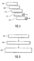
- Fig. 5 illustrates the conventional instruction, bypass, and IDCODE JTAG registers 206, 208, 210, and the switch and chain registers 212, 502 of the present invention.
- Fig. 6 illustrates a process flow in accordance with the present invention.
- Switch register bits in two or more TAP controllers are reset 602 to a known state.
- a logical combination of the outputs of the switch register bits in their reset state controls which of the TAP controllers can be accessed by an external observer.
- writing to the switch register bit of the selected TAP controller results in that bit toggling (i.e., having its current state inverted).
- the new state of the switch register bits is used to produce, or derive, 604 at least one mode signal.
- a next TAP controller is selected 606 for communication with the external observer. In the case of two TAP controllers, the mode signal always selects one of the two TAP controllers.
- a mode bus may be derived, such that a changing value in any switch-register causes the next scheduled TAP controller to be selected. Such examples are described in greater detail below.
- TAP1, TAP2, and TAP3 are TAP controllers.
- TAP1, TAP2, and TAP3 are TAP controllers.
- Each TAP controller has a 1-bit switch register that resets to zero.
- a mode bus is used instead of using a single XOR to make the mode bit (as described above in connection with the example having two TAP controllers).
- TAP1 is selected by default, and when the switch register of a selected TAP controller is written, a next controller is selected, for example: TAP 1 ⁇ TAP2 -> TAP3 -> TAP 1 and so on.
- the mode-bus has a width corresponding to ceiling[log2(#TAPs)], which, in this illustrative embodiment, amounts to two bits, and those two bits may be defined as shown in TABLE 1.
- TABLE 1 mode[1:0] selected TAP 00 TAP1 01 TAP2 10 TAP3 11 not used
- the TDI and TMS inputs are gated by a s-mput AND gate (see TABLE 1).
- Two of the inputs are the mode[1] and mode[0] bits, with some inverting, such that only the selected TAP controller receives a TDI or TMS signal from the top-level pins.
- the three TDO signals are multiplexed using the mode[1:0] bits such that only the selected TAP controller provides a TDO signal to the top-level pins.
- Various well-known circuits can be used to implement the foregoing logic and multiplexing.
- the input-output table (see TABLE 2) for the mode-bus can be easily synthesized and yields an relatively small number of logic gates.
- TAP1 to TAP4 in this example
- TAP1 is selected by default.
- a next controller is selected, for example: TAP1 -> TAP2 -> TAP3 -> TAP4 -> TAP 1 and so on.
- the mode-bus has a width corresponding to ceiling[log2(#TAPs)] (which still amounts to two bits), and the mode bits are defined in TABLE 3.
- TABLE 3 mode[1:0] selected TAP selected TDO (mode-bus is input to 4-to-1 mux) "00" TAP1 tdo1 "01” TAP2 tdo2 "10" TAP3 tdo3 "11” TAP4 tdo4
- the TDI and TMS inputs are gated by a 3-input AND gate (see TABLE 3). Two of the inputs are the mode[1] and mode[0] bits, with some inverting, such that only the selected TAP controller receives a TDI or TMS signal from the top-level pins. Similarly, the four TDO signals are multiplexed using the mode[1:0] bits such that only the selected TAP controller provides a TDO signal to the top-level pins.
- Various well-known circuits can be used to implement the foregoing logic and multiplexing.
- TAP controllers If more TAP controllers are to be used, then the number of mode bits grows with log2 rate. That is, three mode bits are sufficient for up to eight TAP controllers, four bits are sufficient up to sixteen TAP controllers and so on. The number of defined and used input states also grows slowly, only by two states per added TAP controller.
- every TDI in a chain is configured to receive its signal from two sources, namely: (1) the top-level TDI pin in case it is the TDI of the selected TAP controller, or, the TDO-signal from the preceding TAP controller in case of chaining.
- the complexity does not grow with the addition of more TAP controllers.
- the TDI for any TAP controller in the chain can still only come from two possible sources, which are, as noted above: (1) the top-level TDI for the case of being the TDI of the selected controller, or, (2) from the TDO signal of the preceding TAP controller for the case of being a TDI of a daisy-chained TAP controller.
- the TDO pin is either driven by an individual selected TAP controller (using an n-to-1 multiplexer), or, if all TAP controllers are daisy-chained, the TDO is driven by the TDO-signal from the last TAP in the chain.
- Embodiments of the present invention may use scheduling algorithms other than round-robin, although there are some complexity issues in making the target of a switch programmable.
- the state of the system may be stored in every TAP controller, or in a central place. This is different from the above-described illustrative embodiments wherein the state is encoded in the combined switch/chain bits of the data registers in the TAP controllers.
- TAP controllers on a single chip are accessed, in accordance with the IEEE 1149 specification by maintaining the appearance of having only a single test access port to an outside observer.
- TAP controllers By adding a single bit to a data register of each of a plurality of TAP controllers, along with straightforward combinational glue logic, the plurality of TAP controllers can be accessed without the need for additional chip pins, and without the need for additional TAP controllers.
- By adding a second bit to at least one of the TAP controllers internal derivation of signals suitable for controlling desirable functionality of the plurality of TAP controllers can be achieved. Toggling the state of the added bits in the respective data registers of the plurality of TAP controllers provides the control information for either switching or daisy-chaining of the plurality of TAP controllers.
Abstract
Description
- The present invention relates generally to electronic systems,and more particularly relates to methods and apparatus for connecting multiple test access port controllers on a single integrated circuit through a single test access port.
- Advances in semiconductor manufacturing technology, as well as indigital systems architecture, have resulted in the ability to design and produce larger integrated circuits incorporating much more functionality than has been possible in the past. A particular class of integrated circuits, which incorporate at least several large functional blocks to produce a high level of functionality, is referred to as System on Chip (SoC). Such SoC integrated circuits often include one or more processors along with memory for storing program code that is to be executed by the processors, and one or more circuit blocks for implementing various high-level peripheral functions. Such large, complex, and highly functional integrated circuits present many challenges in terms of design effort and testing.
- In order to reduce the amount of time and effort required to design acomplex integrated circuit such as a SoC, engineers often attempt to re-usefunctional blocks (sometimes referred to as IP cores). Indeed, many design groups maintain libraries of such pre-designed and pre-verified IP cores. To maintain the advantages of using such pre-designed and pre-verified IP cores, it is preferable to not have to modify the internal design of such cores.
- In order to address the requirements for testability, a number of efforts have led to the development of test architectures, such as the JTAG specification which has been formalized by the Institute of Electrical and Electronic Engineers as IEEE Standard 1149.1 Test Access Port and Boundary Scan Architecture. Test access is provided to a whole integrated circuit, or a portion thereof, through a test access port (TAP) controller along with a variety of registers. A TAP controller may be associated with each of a plurality of large functional blocks, such as, for example, IP cores.Some pre-designed IP cores may include TAP controllers, in other instances TAP controllers must be added to an integrated circuit design by the engineers as the one or more IP cores are included in a product design.
- US patent application US6311602 discloses an integrated circuit (IC) having a plurality of TAP controllers. To provide access to individual TAP controllers via the external test data in (TDI) and test data out (TDO) pins, the IC further comprises a chip-level TAP linking module (TLM). Each TAP controller is extended with an extension bit that is monitored by the chip-level TLM. As soon as a TAP controller is informed that access has to be transferred to another TAP controller, it sets its extension bit, thus signalling the chip-level TLM to expect the reception of a configuration instruction in its next data cycle. This configuration instruction controls the transfer of access to the TDI and TDO pin from one TAP controller to another.
- What is needed are methods and apparatus for accessing multiple test access port controllers on a single integrated circuit.
- Briefly, embodiments of the present invention provide circuits and methods for accessing multiple test access port (TAP) controllers on a single chip, which is important for compliance with the IEEE 1149.1 Standard. Embodiments of the present invention achieve compliance by maintaining the appearance of having only a single test access port to an outside observer. By adding a single bit to a data register of each of a plurality of TAP controllers along with straightforward combinational glue logic, the plurality of TAP controllers can be accessed without the need for additional chip pins, and without the need for additional TAP controllers that are arranged in a hierarchy or master-slave combination.
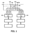
- Fig. 1 is a high-level schematic block diagram of a SoC that includes a pair of IP cores, each having associated TAP controller/JTAG circuitry, and the logic and external connections for switching between each of the pair of IP cores for test access.
- Fig. 2 is a high level block diagram of a SoC that includes a pair of IP cores, each having an associated switch register in accordance with the present invention, and the logic for internally generating a signal used in switching between each of the pair of IP cores for test access.
- Fig. 3 is a high-level schematic block diagram of a SoC having a pair of TAP controllers illustrating the daisy chained data flow therebetween, in accordance with the present invention.
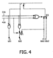
- Fig. 4 is a schematic diagram of logic for implementing the daisy chained data flow illustrated in Fig. 3, and the switching mechanism based on the mode signal.
- Fig. 5 is a high-level schematic block diagram of showing conventional JTAG registers along with the switch register and chain register of the present invention.
- Fig. 6 is a flowchart of an illustrative process in accordance with the present invention.
- When a design includes a plurality of IP cores and associated TAP controllers, it is desirable to be able to control which TAP controller is enabled communicate with an outside observer. It is also desirable to access the multiple TAP controllers while remaining compliant with the IEEE 1149 specification, and without adding additional pins to the integrated circuit. Various embodiments of the present invention allow multiple TAP controllers on a single integrated circuit to be accessed in a controlled manner through a single TAP controller by including a bit in a data register of each of the TAP controllers, along with simple combinational logic. Addition of such user data registers is allowed in accordance with the IEEE 1149 specification.
- Reference herein to "one embodiment", "an embodiment", or similar formulations, means that a particular feature, structure, operation, or characteristic described in connection with the embodiment, is included in at least one embodiment of the present invention. Thus, the appearances of such phrases or formulations herein are not necessarily all referring to the same embodiment. Furthermore, various particular features, structures, operations, or characteristics may be combined in any suitable manner in one or more embodiments.
- The acronym ASIC refers to Application Specific Integrated Circuit.
- The expression "IP core" is context sensitive and may refer to either a design for a high-level functional block (e.g., schematic, hardware description language, netlist), or to an actual physical implementation of the high-level functional block. IP cores may include, in addition to the circuitry for implementation of the desired function, circuitry for implementation of test and debug facilities.
- The acronym JTAG refers to the Joint Test Action Group. The Institute of Electrical and Electronic Engineers (IEEE) has approved IEEE Standard 1149.1, Test Access Port and Boundary Scan Architecture.
- The acronym SoC refers to a System on a Chip, with SoCs being the plural of SoC.
- The terms chip, semiconductor device, integrated circuit, LSI device, monolithic integrated circuit, ASIC, SoC, microelectronic device, and similar expressions are sometimes used interchangeably in this field. Microelectronic device may be considered to be the broadest term, encompassing the others. With respect to these microelectronic devices, signals are coupled between them and other circuit elements via physical, electrically conductive connections. The point of connection is sometimes referred to as an input, output, terminal, line, pin, pad, port, interface, or similar variants and combinations.
- A JTAG compliant device includes pins for clock, input data, output data, and mode selection, referred to, respectively, as TCK, TDI, TDO, and TMS. TCK refers to Test Clock Input which is a terminal of the JTAG compliant device that receives a clock signal separate from the system clock. TDI refers to a Test Data In which is a terminal through which data is shifted into the JTAG compliant device. TDO refers to Test Data Out which is a terminal through which data is shifted out of the JTAG compliant device. TMS refers to Test Mode Select which is a terminal which receives data for determining which of one or more test modes in which the JTAG compliant device is to operate. A JTAG compliant device may be any type of integrated circuit such as, for example, a microprocessor, an ASIC, or a SoC. A JTAG compliant device may also include a pin to receive a low active reset signal, referred to as TRST#. JTAG compliant devices include a boundary scan register and a TAP controller. The TAP controller is a state machine that controls the JTAG functions. The boundary scan register is made up of a number of serially connected bits where each of those bits is also coupled to digital pins of the JTAG compliant device. JTAG compliant devices may also include other registers, such as, a data register, an instruction register, and a bypass register.
- The logical facilities defined by the IEEE 1149.1 specification are commonly used for boundary scan testing and for system debug.
- Various embodiments of the present invention provide a mechanism for accessing one or more of the multiple TAP controllers within a SoC, while maintaining compliance with the IEEE 1149.1 specification. Simple embodiments of the present invention allow a programmable switch from a default TAP controller to a second TAP controller. In this way the state of a SoC, as observed from outside the SoC, is compliant with the IEEE 1149.1 specification at start-up (i.e., after a reset has been applied to the system). More complex embodiments allow for arrangements such as switching back and forth between individual TAP controllers; and daisy-chaining all the TAP controllers together.
- An application of the present invention is to provide access to multiple TAP controllers on a single chip while complying with the standard set forth in the IEEE 1149.1 specification. In turn, each TAP controller controls the test-logic (e.g., boundary scan testing) or the debug features of an associated IP core. In accordance with the present invention, no additional controllers (e.g., top-level TAP, hierarchical TAP, Master TAP, or TAP Linking Module) and no additional pins are needed to force a particular mode of operation on the chip. Embodiments of the present invention are programmable through, for example, the standard JTAG ports. Embodiments of the present invention are particularly useful in situations where the design of the TAP controllers and the IP cores are done separately, or at different points in time. Some embodiments of the present invention advantageously provide a modular, scalable approach to integrating multiple TAP controllers into a SoC.
- To understand the context of the present invention, refer to Fig. 1, and consider that an IP integrator wishes to put two or more IP cores on one SoC. The IP cores could be processors, DSPs, highly integrated functional blocks, or any combination of the foregoing. Assume that each of these IP cores has a TAP controller and an associated JTAG module arranged in such a way that this TAP-JTAG combination forms an IEEE 1149.1 compliant device if it were on a chip by itself. A straightforward implementation for observing the two IP cores through a JTAG interface would use logical gating, multiplexing, and a "mode" pin as shown in Fig. 1.
- Referring to Fig. 1, assume that
TAP1 102 is the default TAP controller and that the mode signal received from amode pin 104 is set to zero at start-up. Note that both the TDI and TMS inputs to TAP1 102 andTAP2 106 are logically gated such that when the mode signal is a logical zero,TAP1 102 receives the actual TDI and TMS signals whileTAP2 106 receives zeroes for those inputs; and when the mode signal is a logical one,TAP2 106 receives the actual TDI and TMS signals whileTAP1 102 receives zeroes for those inputs. The physical implementation of such logic circuitry is a matter well understood by those skilled in the art. It is noted that the only output from eitherTAP1 102 orTAP2 106 is TDO. The other pins ofTAP controllers TAP controllers multiplexer 108, as are the two enable signals (not shown) for the tri-state buffer associated with the TDO outputs. It is not an uncommon practice that the TAP controller, JTAG module, and IP core are designed separately, and at different points in time. The IP integrator has the task to connect the standardized interfaces properly. - Referring to Fig. 2, assume that each
JTAG module instruction register 206, abypass register 208, and anIDCODE register 210. The IEEE 1149.1 standard allows extendingJTAG modules switch register 212. Fig. 2 shows aswitch register 212 incorporated into each of the twoJTAG modules XOR gate 214 to produce themode signal 216 that controls the logical gating and multiplexing shown in Fig. 1. That is, the mode signal which is produced within the integrated circuit, in accordance with the present invention, replaces the externally supplied mode signal, and corresponding mode pin, shown in Fig. 1. - In accordance with the present invention, the two TAP controllers will appear to be one TAP controller to an off-chip observer, such as a JTAG probe. This is because the state that updates a data register transitions into the Run-Test-Idle state with one more high-level value on TMS during a TCK clock edge. While the probe is negotiating the JTAG protocol, the hardware reconfigures itself and a different TAP controller is connected to the external interface pins of the SoC. The fact that the protocol can be used during this particular state transition for the purpose of changing the connections of the TAP controllers themselves is used by embodiments of the present invention.
- The nature of JTAG operations is that a new value is shifted into a register while, typically, the old value is shifted out and captured off-chip. In some cases a different value is shifted out, for example, when shifting in a new instruction. In order to have a uniform predictable switching mechanism across multiple JTAG modules, it is desirable that a JTAG probe should not be required to keep track of the current values for different switch registers 212. Therefore, in an embodiment of the present invention, the content of
switch register 212 is inverted when shifting in a logical one. So regardless of the current values of both switch registers 212, if exactly one input is inverted, themode signal 216 will switch. Such an arrangement is suitable for embodiments of the present invention in which two TAP controllers are integrated in a single chip. - Given that it is possible, in accordance with the invention, to switch back and forth between two TAP controllers, it is further desirable to provide for daisy chaining of the TAP controllers. In one illustrative embodiment of daisy chaining, as shown in Figs. 3 and 4, the technique shown in Fig. 2 is extended to provide the data-flow associated daisy chaining. More particularly, the general data flow associated with daisy chaining is shown in Fig. 3 by only presenting the flow from TDI to TDO. To accomplish daisy chaining in accordance with the present invention, a TAP controller (e.g., TAP1 102) is further extended by a one bit data register, referred to hereafter as the chain register. Fig. 5 illustrates the conventional instruction, bypass, and IDCODE JTAG registers 206, 208, 210, and the switch and chain registers 212, 502 of the present invention.
- It is noted that although it is possible to add chain bits to more than one of the plurality of TAP controllers on a single integrated circuit in accordance with the present invention, this increases the complexity of the combinational logic that is required for control. It will be appreciated that those skilled in the art and having the benefit of this disclosure can readily synthesize such control logic and therefore those details are not described further.
- As indicated in Fig. 4, the
chain signal 416 can now be used in addition to themode signal 216 to implement appropriate logical gating and multiplexing for TDI1, TDI2, TDO1 and TDO2. Assuming that mode = 0 when chain = 1, then Fig. 4 is logically equivalent to Fig. 3. It will be appreciated that this is an illustrative embodiment of the present invention, and that the exemplary logic may be different if the value of the mode signal, for example, is chosen to be different. This is well-understood by those skilled in the art. - Fig. 6 illustrates a process flow in accordance with the present invention. Switch register bits in two or more TAP controllers are reset 602 to a known state. A logical combination of the outputs of the switch register bits in their reset state controls which of the TAP controllers can be accessed by an external observer. Subsequently, writing to the switch register bit of the selected TAP controller results in that bit toggling (i.e., having its current state inverted). The new state of the switch register bits is used to produce, or derive, 604 at least one mode signal. Based at least in part on the state of the mode signal(s), a next TAP controller is selected 606 for communication with the external observer. In the case of two TAP controllers, the mode signal always selects one of the two TAP controllers.
- In order to scale beyond two TAP controllers a mode bus may be derived, such that a changing value in any switch-register causes the next scheduled TAP controller to be selected. Such examples are described in greater detail below.
- In the following section an illustrative embodiment having three TAP controllers (referred to as TAP1, TAP2, and TAP3) is described. Each TAP controller has a 1-bit switch register that resets to zero. Instead of using a single XOR to make the mode bit (as described above in connection with the example having two TAP controllers), a mode bus is used.
- With respect to switching between TAP1, TAP2, and TAP3, assume a round-robin scheduling algorithm is implemented to provide access between all the TAP controllers. (It is noted that selecting one out of many TAPs is a different function than chaining, and each of these functions is desirable for different purposes. Various embodiments of the present invention support both selecting and chaining.) In this illustrative embodiment TAP1 is selected by default, and when the switch register of a selected TAP controller is written, a next controller is selected, for example: TAP 1 → TAP2 -> TAP3 -> TAP 1 and so on. The mode-bus has a width corresponding to ceiling[log2(#TAPs)], which, in this illustrative embodiment, amounts to two bits, and those two bits may be defined as shown in TABLE 1.
TABLE 1 mode[1:0] selected TAP 00 TAP1 01 TAP2 10 TAP3 11 not used - The logic for the mode-bus is solely dependent on the value of the three switch register bits, S1, S2 and S3, as shown in TABLE 2.
TABLE 2 inputs S3 S2 S1 select, mode output Operation in this mode: 0 0 0 TAP, 00 S 1 switch makes input = 0 0 1 0 0 1 TAP2, 01 S2 switch makes input = 0 1 1 0 1 1 TAP3, 10 S3 switch makes input = 1 1 1 1 1 1 TAP1, 00 S 1 switch makes input = 1 1 0 1 1 0 TAP2,01 S2 switch makes input = 1 0 1 0 0 TAP3, 10 S3 switch makes input = 0 0 0 others not used remaining input combinations not used - In this illustrative embodiment, the TDI and TMS inputs are gated by a s-mput AND gate (see TABLE 1). Two of the inputs are the mode[1] and mode[0] bits, with some inverting, such that only the selected TAP controller receives a TDI or TMS signal from the top-level pins. Similarly, the three TDO signals are multiplexed using the mode[1:0] bits such that only the selected TAP controller provides a TDO signal to the top-level pins. Various well-known circuits can be used to implement the foregoing logic and multiplexing. The input-output table (see TABLE 2) for the mode-bus can be easily synthesized and yields an relatively small number of logic gates.
- In the following section an illustrative embodiment having four TAP controllers (referred to as TAP1 to TAP4 in this example) is described.
- With respect to switching between the various TAP controllers, assume round-robin scheduling is implemented between all TAP controllers. In this illustrative embodiment TAP1 is selected by default. When the switch register of the selected TAP controller is written, a next controller is selected, for example: TAP1 -> TAP2 -> TAP3 -> TAP4 -> TAP 1 and so on.
- In the illustrative embodiment the mode-bus has a width corresponding to ceiling[log2(#TAPs)] (which still amounts to two bits), and the mode bits are defined in TABLE 3.
TABLE 3 mode[1:0] selected TAP selected TDO (mode-bus is input to 4-to-1 mux) "00" TAP1 tdo1 "01" TAP2 tdo2 "10" TAP3 tdo3 "11" TAP4 tdo4 - The logic for the mode-bus is solely dependent on the value of the four switch register bits, S1, S2, S3 and S4, as shown in TABLE 4.
TABLE 4 inputs S4 S3 S2 S1 select, mode output Operation in this mode 0 0 0 0 TAP1, 00 S1 switch makes input = 0 0 0 1 0 0 0 1 TAP2, 01 S2 switch makes input = 0 0 1 1 0 0 1 1 TAP3, 10 S3 switch makes input = 0 1 1 1 0 1 1 1 TAP4, 11 S4 switch makes input = 1 1 1 1 1 1 1 1 TAP1, 00 S1 switch makes input = 1 1 1 0 1 1 1 0 TAP2, 01 S2 switch makes input = 1 1 0 0 1 1 0 0 TAP3, 10 S3 switch makes input = 1 0 0 0 1 0 0 0 TAP4, 11 S4 switch makes input = 0 0 0 0 others not used remaining input states not used - It is noted that there are a number of unused input combinations (also referred to as input states).
- In this illustrative embodiment, the TDI and TMS inputs are gated by a 3-input AND gate (see TABLE 3). Two of the inputs are the mode[1] and mode[0] bits, with some inverting, such that only the selected TAP controller receives a TDI or TMS signal from the top-level pins. Similarly, the four TDO signals are multiplexed using the mode[1:0] bits such that only the selected TAP controller provides a TDO signal to the top-level pins. Various well-known circuits can be used to implement the foregoing logic and multiplexing.
- If more TAP controllers are to be used, then the number of mode bits grows with log2 rate. That is, three mode bits are sufficient for up to eight TAP controllers, four bits are sufficient up to sixteen TAP controllers and so on. The number of defined and used input states also grows slowly, only by two states per added TAP controller.
- With respect to chaining between the various TAP controllers, rather than switching as described above, the following changes are needed: every TDI in a chain is configured to receive its signal from two sources, namely: (1) the top-level TDI pin in case it is the TDI of the selected TAP controller, or, the TDO-signal from the preceding TAP controller in case of chaining. There are small provisions at the beginning and the end of the chain, but the complexity does not grow with the addition of more TAP controllers. For example, even with a chain containing ten TAP controllers, the TDI for any TAP controller in the chain can still only come from two possible sources, which are, as noted above: (1) the top-level TDI for the case of being the TDI of the selected controller, or, (2) from the TDO signal of the preceding TAP controller for the case of being a TDI of a daisy-chained TAP controller. Similarly, in this illustrative example, the TDO pin is either driven by an individual selected TAP controller (using an n-to-1 multiplexer), or, if all TAP controllers are daisy-chained, the TDO is driven by the TDO-signal from the last TAP in the chain.
- Embodiments of the present invention may use scheduling algorithms other than round-robin, although there are some complexity issues in making the target of a switch programmable. In such a scenario, the state of the system may be stored in every TAP controller, or in a central place. This is different from the above-described illustrative embodiments wherein the state is encoded in the combined switch/chain bits of the data registers in the TAP controllers.
- Multiple test access port (TAP) controllers on a single chip are accessed, in accordance with the IEEE 1149 specification by maintaining the appearance of having only a single test access port to an outside observer. By adding a single bit to a data register of each of a plurality of TAP controllers, along with straightforward combinational glue logic, the plurality of TAP controllers can be accessed without the need for additional chip pins, and without the need for additional TAP controllers. By adding a second bit to at least one of the TAP controllers, internal derivation of signals suitable for controlling desirable functionality of the plurality of TAP controllers can be achieved. Toggling the state of the added bits in the respective data registers of the plurality of TAP controllers provides the control information for either switching or daisy-chaining of the plurality of TAP controllers.
- It is to be understood that the present invention is not limited to the embodiments described above, but encompasses any and all embodiments within the scope of the subjoined Claims.
Claims (12)
- A method of coupling a plurality of test access port, TAP, controllers (102, 106) that each comprise a one-bit register (212) for storing a first register bit to a single external interface, comprising:a) resetting the first register bit in the one-bit register (212) of each of plurality of TAP controllers (102,106) to a known state;b) producing a first signal (216);c) selecting one of the plurality of TAP controllers (102, 106) based, at least in part, on the first signal;d) coupling an external input terminal (TDI) to an input terminal of the selected one of the plurality of TAP controllers (102, 106); ande) coupling an output terminal (TDO) of the selected one of the plurality of TAP controllers (102, 106) to an external output terminal;characterized by producing the first signal (216) based, at least in part, on the state of the first register bit in each of the plurality of TAP controllers (102,106).
- The method of Claim 1, wherein each TAP controller (102, 106) comprises a finite state machine and a plurality of registers (206, 208, 210, 212).
- The method of Claim 2, further comprising toggling the first register bit in the selected one of the plurality of TAP controllers (102, 106); and repeating steps b) through e).
- The method of Claim 3, further comprising providing a clock signal, a test mode selection signal (104), and a test reset signal to each of the plurality of TAP controllers (102, 106).
- The method of Claim 3, wherein the plurality of TAP controllers (102, 106) are disposed on a single integrated circuit.
- The method of Claim 5, wherein the first signal (216) is produced within the single integrated circuit.
- The method of Claim 6, further comprising receiving, from a source external to the single integrated circuit, a clock signal.
- An integrated circuit, comprising:a plurality of functional blocks, each functional block having a test access port, TAP, controller (102, 106) coupled thereto; each TAP controller (102, 106) including a one-bit register (212) for storing a first register bit, each first register bit adapted to produce a known output state in response to a reset signal, each first register bit further adapted to toggle in response to a register write operation; androuting logic (214) adapted to selectively provide a communication path between an external input signal source (TDI) and an input terminal of a selected one of the TAP controllers;characterized in that the routing logic (214) is adapted to selectively provide said communication path based at least in part on the state of the plurality of first register bits.
- The integrated circuit of Claim 8, wherein the routing logic is further adapted to selectively provide, based at least in part on the state of the plurality of first register bits, a communication path between an external output terminal and an output terminal (TDO) of the selected on the TAP controllers (102, 106).
- The integrated circuit of Claim 8, wherein at least one TAP controller (102, 106) further includes a second one-bit register (502) for storing a second register bit, and wherein the routing logic is further adapted to provide the output of a first TAP controller (102) as an input to a second TAP controller (106), based at least in part on the state of the first and second register bits.
- The integrated circuit of Claim 9, wherein a transition between the selectively provided communication paths is transparent to an external observer.
- The integrated circuit of Claim 8, wherein each one-bit register (212) forms a part of a data register of the respective TAP controllers (102, 106).
Applications Claiming Priority (3)
| Application Number | Priority Date | Filing Date | Title |
|---|---|---|---|
| US43539502P | 2002-12-20 | 2002-12-20 | |
| US435395P | 2002-12-20 | ||
| PCT/IB2003/005950 WO2004057357A1 (en) | 2002-12-20 | 2003-12-15 | Connecting multiple test access port controllers through a single test access port |
Publications (2)
| Publication Number | Publication Date |
|---|---|
| EP1579229A1 EP1579229A1 (en) | 2005-09-28 |
| EP1579229B1 true EP1579229B1 (en) | 2006-11-22 |
Family
ID=32682232
Family Applications (1)
| Application Number | Title | Priority Date | Filing Date |
|---|---|---|---|
| EP03780425A Expired - Lifetime EP1579229B1 (en) | 2002-12-20 | 2003-12-15 | Connecting multiple test access port controllers through a single test access port |
Country Status (10)
| Country | Link |
|---|---|
| US (1) | US7426670B2 (en) |
| EP (1) | EP1579229B1 (en) |
| JP (1) | JP2006510980A (en) |
| KR (1) | KR20050084395A (en) |
| CN (1) | CN100442074C (en) |
| AT (1) | ATE346309T1 (en) |
| AU (1) | AU2003288584A1 (en) |
| DE (1) | DE60309931T2 (en) |
| TW (1) | TWI298099B (en) |
| WO (1) | WO2004057357A1 (en) |
Families Citing this family (25)
| Publication number | Priority date | Publication date | Assignee | Title |
|---|---|---|---|---|
| US7417450B2 (en) * | 2005-12-02 | 2008-08-26 | Texas Instruments Incorporated | Testing combinational logic die with bidirectional TDI-TMS/TDO chanel circuit |
| US7346821B2 (en) * | 2003-08-28 | 2008-03-18 | Texas Instrument Incorporated | IC with JTAG port, linking module, and off-chip TAP interface |
| GB0526448D0 (en) | 2005-12-23 | 2006-02-08 | Advanced Risc Mach Ltd | Diagnostic mode switching |
| KR100809259B1 (en) * | 2006-10-04 | 2008-03-03 | 삼성전기주식회사 | Device for interface of communication module |
| JP2008310792A (en) * | 2007-05-11 | 2008-12-25 | Nec Electronics Corp | Test circuit |
| JP5022110B2 (en) * | 2007-06-05 | 2012-09-12 | ルネサスエレクトロニクス株式会社 | Semiconductor integrated circuit |
| US8078898B2 (en) * | 2007-06-07 | 2011-12-13 | Texas Instruments Incorporated | Synchronizing TAP controllers with sequence on TMS lead |
| US8046650B2 (en) * | 2008-03-14 | 2011-10-25 | Texas Instruments Incorporated | TAP with control circuitry connected to device address port |
| US7783819B2 (en) * | 2008-03-31 | 2010-08-24 | Intel Corporation | Integrating non-peripheral component interconnect (PCI) resources into a personal computer system |
| EP2331979B1 (en) * | 2008-09-26 | 2012-07-04 | Nxp B.V. | Method for testing a partially assembled multi-die device, integrated circuit die and multi-die device |
| US8694844B2 (en) * | 2010-07-29 | 2014-04-08 | Texas Instruments Incorporated | AT speed TAP with dual port router and command circuit |
| WO2013048528A1 (en) * | 2011-10-01 | 2013-04-04 | Intel Corporation | Packetizing jtag across industry standard interfaces |
| US9323633B2 (en) * | 2013-03-28 | 2016-04-26 | Stmicroelectronics, Inc. | Dual master JTAG method, circuit, and system |
| CN105247821B (en) * | 2013-06-28 | 2018-11-06 | 英特尔公司 | Mechanism for controlling the utilization of resources using adaptive routing |
| US20150046763A1 (en) * | 2013-08-12 | 2015-02-12 | Apple Inc. | Apparatus and Method for Controlling Internal Test Controllers |
| US9810739B2 (en) | 2015-10-27 | 2017-11-07 | Andes Technology Corporation | Electronic system, system diagnostic circuit and operation method thereof |
| KR102474620B1 (en) * | 2016-01-25 | 2022-12-05 | 삼성전자주식회사 | Semiconductor device, semiconductor system and method for operating semiconductor device |
| CN108226740B (en) * | 2016-12-09 | 2020-06-02 | 英业达科技有限公司 | Expansion circuit board for providing interface of expansion joint test working group |
| US10386411B2 (en) | 2017-08-23 | 2019-08-20 | Stmicroelectronics International N.V. | Sequential test access port selection in a JTAG interface |
| CN108829547B (en) * | 2018-05-15 | 2021-11-16 | 中国船舶重工集团公司第七一九研究所 | Computer controller of ocean platform and implementation method thereof |
| US10571518B1 (en) * | 2018-09-26 | 2020-02-25 | Nxp B.V. | Limited pin test interface with analog test bus |
| CN109406902B (en) * | 2018-11-28 | 2021-03-19 | 中科曙光信息产业成都有限公司 | Logic scanning aging test system |
| CN113627106B (en) * | 2021-08-04 | 2022-02-15 | 北京华大九天科技股份有限公司 | Simulation method and device of multi-bit register and electronic equipment |
| CN116774018B (en) * | 2023-08-22 | 2023-11-28 | 北京芯驰半导体科技有限公司 | Chip testing method and device and electronic equipment |
| CN117741411A (en) * | 2024-02-19 | 2024-03-22 | 西安简矽技术有限公司 | Chip adjusting system and method |
Family Cites Families (12)
| Publication number | Priority date | Publication date | Assignee | Title |
|---|---|---|---|---|
| US5132635A (en) * | 1991-03-05 | 1992-07-21 | Ast Research, Inc. | Serial testing of removable circuit boards on a backplane bus |
| US5627842A (en) * | 1993-01-21 | 1997-05-06 | Digital Equipment Corporation | Architecture for system-wide standardized intra-module and inter-module fault testing |
| FI100136B (en) * | 1993-10-01 | 1997-09-30 | Nokia Telecommunications Oy | A method for testing an integrated circuit and an integrated circuit |
| EP0826974B1 (en) * | 1996-08-30 | 2005-10-19 | Texas Instruments Incorporated | Device for testing integrated circuits |
| US6804725B1 (en) * | 1996-08-30 | 2004-10-12 | Texas Instruments Incorporated | IC with state machine controlled linking module |
| US6032279A (en) * | 1997-11-07 | 2000-02-29 | Atmel Corporation | Boundary scan system with address dependent instructions |
| US6385749B1 (en) * | 1999-04-01 | 2002-05-07 | Koninklijke Philips Electronics N.V. (Kpenv) | Method and arrangement for controlling multiple test access port control modules |
| US6311302B1 (en) * | 1999-04-01 | 2001-10-30 | Philips Semiconductor, Inc. | Method and arrangement for hierarchical control of multiple test access port control modules |
| US6886121B2 (en) * | 2000-01-18 | 2005-04-26 | Cadence Design Systems, Inc. | Hierarchical test circuit structure for chips with multiple circuit blocks |
| US6961884B1 (en) * | 2000-06-12 | 2005-11-01 | Altera Corporation | JTAG mirroring circuitry and methods |
| US6829730B2 (en) * | 2001-04-27 | 2004-12-07 | Logicvision, Inc. | Method of designing circuit having multiple test access ports, circuit produced thereby and method of using same |
| US6968408B2 (en) * | 2002-08-08 | 2005-11-22 | Texas Instruments Incorporated | Linking addressable shadow port and protocol for serial bus networks |
-
2003
- 2003-12-15 EP EP03780425A patent/EP1579229B1/en not_active Expired - Lifetime
- 2003-12-15 CN CNB2003801068393A patent/CN100442074C/en not_active Expired - Fee Related
- 2003-12-15 WO PCT/IB2003/005950 patent/WO2004057357A1/en active IP Right Grant
- 2003-12-15 US US10/539,104 patent/US7426670B2/en not_active Expired - Lifetime
- 2003-12-15 JP JP2004561840A patent/JP2006510980A/en active Pending
- 2003-12-15 AU AU2003288584A patent/AU2003288584A1/en not_active Abandoned
- 2003-12-15 DE DE60309931T patent/DE60309931T2/en not_active Expired - Lifetime
- 2003-12-15 AT AT03780425T patent/ATE346309T1/en not_active IP Right Cessation
- 2003-12-15 KR KR1020057011239A patent/KR20050084395A/en not_active Application Discontinuation
- 2003-12-17 TW TW092135815A patent/TWI298099B/en not_active IP Right Cessation
Also Published As
| Publication number | Publication date |
|---|---|
| JP2006510980A (en) | 2006-03-30 |
| CN100442074C (en) | 2008-12-10 |
| DE60309931T2 (en) | 2007-09-13 |
| ATE346309T1 (en) | 2006-12-15 |
| KR20050084395A (en) | 2005-08-26 |
| US7426670B2 (en) | 2008-09-16 |
| TW200500620A (en) | 2005-01-01 |
| DE60309931D1 (en) | 2007-01-04 |
| AU2003288584A1 (en) | 2004-07-14 |
| US20060090110A1 (en) | 2006-04-27 |
| EP1579229A1 (en) | 2005-09-28 |
| WO2004057357A1 (en) | 2004-07-08 |
| CN1729401A (en) | 2006-02-01 |
| TWI298099B (en) | 2008-06-21 |
Similar Documents
| Publication | Publication Date | Title |
|---|---|---|
| EP1579229B1 (en) | Connecting multiple test access port controllers through a single test access port | |
| US10162001B2 (en) | TAP and gating enable, CaptureDR, capture, and gated CaptureDR signals | |
| US10649029B2 (en) | TCKC/TMSC counter, gating circuitry for selection, deselection, technology specific outputs | |
| US10281524B2 (en) | Test partition external input/output interface control for test partitions in a semiconductor | |
| JP4422427B2 (en) | Single chip system and method for testing / debugging this system | |
| US4799004A (en) | Transfer circuit for operation test of LSI systems | |
| US6314539B1 (en) | Boundary-scan register cell with bypass circuit | |
| US6499124B1 (en) | Intest security circuit for boundary-scan architecture | |
| US6378090B1 (en) | Hierarchical test access port architecture for electronic circuits including embedded core having built-in test access port | |
| US5260948A (en) | Bidirectional boundary-scan circuit | |
| JPS6329276A (en) | Logic lsi | |
| US5729553A (en) | Semiconductor integrated circuit with a testable block | |
| US5077740A (en) | Logic circuit having normal input/output data paths disabled when test data is transferred during macrocell testing | |
| EP0699920A2 (en) | Semiconductor integrated circuit with a testable block | |
| US20030046625A1 (en) | Method and apparatus for efficient control of multiple tap controllers | |
| JP2003121497A (en) | Scan path circuit for logic circuit test and integrated circuit device provided with it | |
| EP0370194A2 (en) | Reconfigurable register bit slice | |
| JP2004004047A (en) | Input/output characterization chain for integrated circuit | |
| US20030149926A1 (en) | Single scan chain in hierarchiacally bisted designs | |
| KR20010108796A (en) | System-on-chip having shift register chain for test embedded core | |
| JP2001074811A (en) | Semiconductor integrated circuit | |
| JPH0358143A (en) | Scan in/out logic circuit for lsi | |
| JP2000009800A (en) | Scan test circuit and semiconductor device equipped with the same and scan testing method therefor | |
| JPH03249574A (en) | Semiconductor logical unit containing diagnostic scan register |
Legal Events
| Date | Code | Title | Description |
|---|---|---|---|
| PUAI | Public reference made under article 153(3) epc to a published international application that has entered the european phase |
Free format text: ORIGINAL CODE: 0009012 |
|
| 17P | Request for examination filed |
Effective date: 20050720 |
|
| AK | Designated contracting states |
Kind code of ref document: A1 Designated state(s): AT BE BG CH CY CZ DE DK EE ES FI FR GB GR HU IE IT LI LU MC NL PT RO SE SI SK TR |
|
| AX | Request for extension of the european patent |
Extension state: AL LT LV MK |
|
| DAX | Request for extension of the european patent (deleted) | ||
| GRAP | Despatch of communication of intention to grant a patent |
Free format text: ORIGINAL CODE: EPIDOSNIGR1 |
|
| GRAS | Grant fee paid |
Free format text: ORIGINAL CODE: EPIDOSNIGR3 |
|
| GRAA | (expected) grant |
Free format text: ORIGINAL CODE: 0009210 |
|
| AK | Designated contracting states |
Kind code of ref document: B1 Designated state(s): AT BE BG CH CY CZ DE DK EE ES FI FR GB GR HU IE IT LI LU MC NL PT RO SE SI SK TR |
|
| PG25 | Lapsed in a contracting state [announced via postgrant information from national office to epo] |
Ref country code: FI Free format text: LAPSE BECAUSE OF FAILURE TO SUBMIT A TRANSLATION OF THE DESCRIPTION OR TO PAY THE FEE WITHIN THE PRESCRIBED TIME-LIMIT Effective date: 20061122 Ref country code: CH Free format text: LAPSE BECAUSE OF FAILURE TO SUBMIT A TRANSLATION OF THE DESCRIPTION OR TO PAY THE FEE WITHIN THE PRESCRIBED TIME-LIMIT Effective date: 20061122 Ref country code: BE Free format text: LAPSE BECAUSE OF FAILURE TO SUBMIT A TRANSLATION OF THE DESCRIPTION OR TO PAY THE FEE WITHIN THE PRESCRIBED TIME-LIMIT Effective date: 20061122 Ref country code: SI Free format text: LAPSE BECAUSE OF FAILURE TO SUBMIT A TRANSLATION OF THE DESCRIPTION OR TO PAY THE FEE WITHIN THE PRESCRIBED TIME-LIMIT Effective date: 20061122 Ref country code: AT Free format text: LAPSE BECAUSE OF FAILURE TO SUBMIT A TRANSLATION OF THE DESCRIPTION OR TO PAY THE FEE WITHIN THE PRESCRIBED TIME-LIMIT Effective date: 20061122 Ref country code: IT Free format text: LAPSE BECAUSE OF FAILURE TO SUBMIT A TRANSLATION OF THE DESCRIPTION OR TO PAY THE FEE WITHIN THE PRESCRIBED TIME-LIMIT;WARNING: LAPSES OF ITALIAN PATENTS WITH EFFECTIVE DATE BEFORE 2007 MAY HAVE OCCURRED AT ANY TIME BEFORE 2007. THE CORRECT EFFECTIVE DATE MAY BE DIFFERENT FROM THE ONE RECORDED. Effective date: 20061122 Ref country code: LI Free format text: LAPSE BECAUSE OF FAILURE TO SUBMIT A TRANSLATION OF THE DESCRIPTION OR TO PAY THE FEE WITHIN THE PRESCRIBED TIME-LIMIT Effective date: 20061122 Ref country code: NL Free format text: LAPSE BECAUSE OF FAILURE TO SUBMIT A TRANSLATION OF THE DESCRIPTION OR TO PAY THE FEE WITHIN THE PRESCRIBED TIME-LIMIT Effective date: 20061122 Ref country code: CZ Free format text: LAPSE BECAUSE OF FAILURE TO SUBMIT A TRANSLATION OF THE DESCRIPTION OR TO PAY THE FEE WITHIN THE PRESCRIBED TIME-LIMIT Effective date: 20061122 Ref country code: SK Free format text: LAPSE BECAUSE OF FAILURE TO SUBMIT A TRANSLATION OF THE DESCRIPTION OR TO PAY THE FEE WITHIN THE PRESCRIBED TIME-LIMIT Effective date: 20061122 Ref country code: RO Free format text: LAPSE BECAUSE OF FAILURE TO SUBMIT A TRANSLATION OF THE DESCRIPTION OR TO PAY THE FEE WITHIN THE PRESCRIBED TIME-LIMIT Effective date: 20061122 |
|
| REG | Reference to a national code |
Ref country code: GB Ref legal event code: FG4D |
|
| PG25 | Lapsed in a contracting state [announced via postgrant information from national office to epo] |
Ref country code: IE Free format text: LAPSE BECAUSE OF NON-PAYMENT OF DUE FEES Effective date: 20061215 |
|
| REG | Reference to a national code |
Ref country code: CH Ref legal event code: EP |
|
| REG | Reference to a national code |
Ref country code: IE Ref legal event code: FG4D |
|
| PG25 | Lapsed in a contracting state [announced via postgrant information from national office to epo] |
Ref country code: MC Free format text: LAPSE BECAUSE OF NON-PAYMENT OF DUE FEES Effective date: 20061231 |
|
| REF | Corresponds to: |
Ref document number: 60309931 Country of ref document: DE Date of ref document: 20070104 Kind code of ref document: P |
|
| PG25 | Lapsed in a contracting state [announced via postgrant information from national office to epo] |
Ref country code: DK Free format text: LAPSE BECAUSE OF FAILURE TO SUBMIT A TRANSLATION OF THE DESCRIPTION OR TO PAY THE FEE WITHIN THE PRESCRIBED TIME-LIMIT Effective date: 20070222 Ref country code: BG Free format text: LAPSE BECAUSE OF FAILURE TO SUBMIT A TRANSLATION OF THE DESCRIPTION OR TO PAY THE FEE WITHIN THE PRESCRIBED TIME-LIMIT Effective date: 20070222 Ref country code: SE Free format text: LAPSE BECAUSE OF FAILURE TO SUBMIT A TRANSLATION OF THE DESCRIPTION OR TO PAY THE FEE WITHIN THE PRESCRIBED TIME-LIMIT Effective date: 20070222 |
|
| PG25 | Lapsed in a contracting state [announced via postgrant information from national office to epo] |
Ref country code: ES Free format text: LAPSE BECAUSE OF FAILURE TO SUBMIT A TRANSLATION OF THE DESCRIPTION OR TO PAY THE FEE WITHIN THE PRESCRIBED TIME-LIMIT Effective date: 20070305 |
|
| PG25 | Lapsed in a contracting state [announced via postgrant information from national office to epo] |
Ref country code: PT Free format text: LAPSE BECAUSE OF FAILURE TO SUBMIT A TRANSLATION OF THE DESCRIPTION OR TO PAY THE FEE WITHIN THE PRESCRIBED TIME-LIMIT Effective date: 20070423 |
|
| NLV1 | Nl: lapsed or annulled due to failure to fulfill the requirements of art. 29p and 29m of the patents act | ||
| ET | Fr: translation filed | ||
| REG | Reference to a national code |
Ref country code: CH Ref legal event code: PL |
|
| PLBE | No opposition filed within time limit |
Free format text: ORIGINAL CODE: 0009261 |
|
| STAA | Information on the status of an ep patent application or granted ep patent |
Free format text: STATUS: NO OPPOSITION FILED WITHIN TIME LIMIT |
|
| 26N | No opposition filed |
Effective date: 20070823 |
|
| PG25 | Lapsed in a contracting state [announced via postgrant information from national office to epo] |
Ref country code: GR Free format text: LAPSE BECAUSE OF FAILURE TO SUBMIT A TRANSLATION OF THE DESCRIPTION OR TO PAY THE FEE WITHIN THE PRESCRIBED TIME-LIMIT Effective date: 20070223 |
|
| PG25 | Lapsed in a contracting state [announced via postgrant information from national office to epo] |
Ref country code: EE Free format text: LAPSE BECAUSE OF FAILURE TO SUBMIT A TRANSLATION OF THE DESCRIPTION OR TO PAY THE FEE WITHIN THE PRESCRIBED TIME-LIMIT Effective date: 20061122 |
|
| PG25 | Lapsed in a contracting state [announced via postgrant information from national office to epo] |
Ref country code: TR Free format text: LAPSE BECAUSE OF FAILURE TO SUBMIT A TRANSLATION OF THE DESCRIPTION OR TO PAY THE FEE WITHIN THE PRESCRIBED TIME-LIMIT Effective date: 20061122 Ref country code: HU Free format text: LAPSE BECAUSE OF FAILURE TO SUBMIT A TRANSLATION OF THE DESCRIPTION OR TO PAY THE FEE WITHIN THE PRESCRIBED TIME-LIMIT Effective date: 20070523 Ref country code: LU Free format text: LAPSE BECAUSE OF NON-PAYMENT OF DUE FEES Effective date: 20061215 |
|
| REG | Reference to a national code |
Ref country code: GB Ref legal event code: 732E |
|
| PG25 | Lapsed in a contracting state [announced via postgrant information from national office to epo] |
Ref country code: CY Free format text: LAPSE BECAUSE OF FAILURE TO SUBMIT A TRANSLATION OF THE DESCRIPTION OR TO PAY THE FEE WITHIN THE PRESCRIBED TIME-LIMIT Effective date: 20061122 |
|
| REG | Reference to a national code |
Ref country code: FR Ref legal event code: TP |
|
| PG25 | Lapsed in a contracting state [announced via postgrant information from national office to epo] |
Ref country code: FR Free format text: LAPSE BECAUSE OF NON-PAYMENT OF DUE FEES Effective date: 20091231 |
|
| PGFP | Annual fee paid to national office [announced via postgrant information from national office to epo] |
Ref country code: GB Payment date: 20121122 Year of fee payment: 10 |
|
| PGFP | Annual fee paid to national office [announced via postgrant information from national office to epo] |
Ref country code: FR Payment date: 20130130 Year of fee payment: 10 |
|
| GBPC | Gb: european patent ceased through non-payment of renewal fee |
Effective date: 20131215 |
|
| REG | Reference to a national code |
Ref country code: FR Ref legal event code: ST Effective date: 20140829 |
|
| PG25 | Lapsed in a contracting state [announced via postgrant information from national office to epo] |
Ref country code: FR Free format text: LAPSE BECAUSE OF NON-PAYMENT OF DUE FEES Effective date: 20131231 Ref country code: GB Free format text: LAPSE BECAUSE OF NON-PAYMENT OF DUE FEES Effective date: 20131215 |
|
| REG | Reference to a national code |
Ref country code: DE Ref legal event code: R082 Ref document number: 60309931 Country of ref document: DE Representative=s name: MUELLER-BORE & PARTNER PATENTANWAELTE PARTG MB, DE Ref country code: DE Ref legal event code: R081 Ref document number: 60309931 Country of ref document: DE Owner name: LLL HOLDINGS 6, LLC, WILMINGTON, US Free format text: FORMER OWNER: NXP B.V., EINDHOVEN, NL Ref country code: DE Ref legal event code: R081 Ref document number: 60309931 Country of ref document: DE Owner name: III HOLDINGS 6, LLC, WILMINGTON, US Free format text: FORMER OWNER: NXP B.V., EINDHOVEN, NL |
|
| REG | Reference to a national code |
Ref country code: DE Ref legal event code: R082 Ref document number: 60309931 Country of ref document: DE Representative=s name: MUELLER-BORE & PARTNER PATENTANWAELTE PARTG MB, DE Ref country code: DE Ref legal event code: R081 Ref document number: 60309931 Country of ref document: DE Owner name: III HOLDINGS 6, LLC, WILMINGTON, US Free format text: FORMER OWNER: LLL HOLDINGS 6, LLC, WILMINGTON, DEL., US |
|
| PGFP | Annual fee paid to national office [announced via postgrant information from national office to epo] |
Ref country code: DE Payment date: 20211228 Year of fee payment: 19 |
|
| REG | Reference to a national code |
Ref country code: DE Ref legal event code: R119 Ref document number: 60309931 Country of ref document: DE |
|
| PG25 | Lapsed in a contracting state [announced via postgrant information from national office to epo] |
Ref country code: DE Free format text: LAPSE BECAUSE OF NON-PAYMENT OF DUE FEES Effective date: 20230701 |