EP1599886B1 - Electronic disabling device - Google Patents
Electronic disabling device Download PDFInfo
- Publication number
- EP1599886B1 EP1599886B1 EP04710296A EP04710296A EP1599886B1 EP 1599886 B1 EP1599886 B1 EP 1599886B1 EP 04710296 A EP04710296 A EP 04710296A EP 04710296 A EP04710296 A EP 04710296A EP 1599886 B1 EP1599886 B1 EP 1599886B1
- Authority
- EP
- European Patent Office
- Prior art keywords
- capacitance
- voltage
- target
- discharging
- switch
- Prior art date
- Legal status (The legal status is an assumption and is not a legal conclusion. Google has not performed a legal analysis and makes no representation as to the accuracy of the status listed.)
- Expired - Lifetime
Links
- 238000004804 winding Methods 0.000 claims description 46
- 238000000034 method Methods 0.000 claims description 39
- 238000007599 discharging Methods 0.000 claims description 33
- 230000015556 catabolic process Effects 0.000 claims description 21
- 230000004044 response Effects 0.000 claims description 14
- 230000004913 activation Effects 0.000 claims description 8
- 210000002027 skeletal muscle Anatomy 0.000 claims description 3
- 230000033001 locomotion Effects 0.000 claims 4
- 238000012358 sourcing Methods 0.000 claims 4
- 230000008602 contraction Effects 0.000 claims 2
- 239000003990 capacitor Substances 0.000 description 68
- 101500022510 Lithobates catesbeianus GnRH-associated peptide 2 Proteins 0.000 description 19
- 238000010586 diagram Methods 0.000 description 19
- 101500023488 Lithobates catesbeianus GnRH-associated peptide 1 Proteins 0.000 description 17
- 230000006870 function Effects 0.000 description 11
- 101100282115 Candida albicans (strain SC5314 / ATCC MYA-2876) HIP1 gene Proteins 0.000 description 8
- 238000013461 design Methods 0.000 description 8
- 101150112629 gap3 gene Proteins 0.000 description 8
- 230000008901 benefit Effects 0.000 description 6
- 230000007423 decrease Effects 0.000 description 6
- 238000004146 energy storage Methods 0.000 description 4
- 230000003750 conditioning effect Effects 0.000 description 3
- 238000010304 firing Methods 0.000 description 3
- 210000003205 muscle Anatomy 0.000 description 3
- 230000008672 reprogramming Effects 0.000 description 3
- -1 E1 to E2 Proteins 0.000 description 2
- WHXSMMKQMYFTQS-UHFFFAOYSA-N Lithium Chemical compound [Li] WHXSMMKQMYFTQS-UHFFFAOYSA-N 0.000 description 2
- 241001465754 Metazoa Species 0.000 description 2
- 238000013459 approach Methods 0.000 description 2
- 238000004891 communication Methods 0.000 description 2
- 239000004020 conductor Substances 0.000 description 2
- 230000009977 dual effect Effects 0.000 description 2
- 230000000694 effects Effects 0.000 description 2
- 229910052744 lithium Inorganic materials 0.000 description 2
- 238000012544 monitoring process Methods 0.000 description 2
- 230000004118 muscle contraction Effects 0.000 description 2
- 230000003287 optical effect Effects 0.000 description 2
- 230000003071 parasitic effect Effects 0.000 description 2
- 230000009467 reduction Effects 0.000 description 2
- 239000000523 sample Substances 0.000 description 2
- 238000004458 analytical method Methods 0.000 description 1
- 230000005540 biological transmission Effects 0.000 description 1
- 230000004397 blinking Effects 0.000 description 1
- 230000001413 cellular effect Effects 0.000 description 1
- 230000001186 cumulative effect Effects 0.000 description 1
- 238000013500 data storage Methods 0.000 description 1
- 230000000779 depleting effect Effects 0.000 description 1
- 239000004744 fabric Substances 0.000 description 1
- 239000000835 fiber Substances 0.000 description 1
- 238000003780 insertion Methods 0.000 description 1
- 230000037431 insertion Effects 0.000 description 1
- 239000011810 insulating material Substances 0.000 description 1
- 238000009413 insulation Methods 0.000 description 1
- 230000003993 interaction Effects 0.000 description 1
- 238000011545 laboratory measurement Methods 0.000 description 1
- 239000010985 leather Substances 0.000 description 1
- 230000007257 malfunction Effects 0.000 description 1
- 238000007726 management method Methods 0.000 description 1
- 238000004519 manufacturing process Methods 0.000 description 1
- 238000005259 measurement Methods 0.000 description 1
- 230000007246 mechanism Effects 0.000 description 1
- 230000005055 memory storage Effects 0.000 description 1
- 230000002232 neuromuscular Effects 0.000 description 1
- 230000000149 penetrating effect Effects 0.000 description 1
- 230000008569 process Effects 0.000 description 1
- 230000002035 prolonged effect Effects 0.000 description 1
- 230000000452 restraining effect Effects 0.000 description 1
- 238000000926 separation method Methods 0.000 description 1
- 210000002460 smooth muscle Anatomy 0.000 description 1
- 239000007787 solid Substances 0.000 description 1
- 230000000638 stimulation Effects 0.000 description 1
- 238000013519 translation Methods 0.000 description 1
Images


Classifications
-
- F—MECHANICAL ENGINEERING; LIGHTING; HEATING; WEAPONS; BLASTING
- F41—WEAPONS
- F41H—ARMOUR; ARMOURED TURRETS; ARMOURED OR ARMED VEHICLES; MEANS OF ATTACK OR DEFENCE, e.g. CAMOUFLAGE, IN GENERAL
- F41H13/00—Means of attack or defence not otherwise provided for
- F41H13/0012—Electrical discharge weapons, e.g. for stunning
-
- F—MECHANICAL ENGINEERING; LIGHTING; HEATING; WEAPONS; BLASTING
- F41—WEAPONS
- F41B—WEAPONS FOR PROJECTING MISSILES WITHOUT USE OF EXPLOSIVE OR COMBUSTIBLE PROPELLANT CHARGE; WEAPONS NOT OTHERWISE PROVIDED FOR
- F41B15/00—Weapons not otherwise provided for, e.g. nunchakus, throwing knives
-
- F—MECHANICAL ENGINEERING; LIGHTING; HEATING; WEAPONS; BLASTING
- F41—WEAPONS
- F41C—SMALLARMS, e.g. PISTOLS, RIFLES; ACCESSORIES THEREFOR
- F41C3/00—Pistols, e.g. revolvers
-
- H—ELECTRICITY
- H05—ELECTRIC TECHNIQUES NOT OTHERWISE PROVIDED FOR
- H05C—ELECTRIC CIRCUITS OR APPARATUS SPECIALLY DESIGNED FOR USE IN EQUIPMENT FOR KILLING, STUNNING, OR GUIDING LIVING BEINGS
- H05C1/00—Circuits or apparatus for generating electric shock effects
- H05C1/04—Circuits or apparatus for generating electric shock effects providing pulse voltages
Definitions
- the present invention relates to devices for disabling an animal or human target; and to methods for providing an electric current through electrodes and the target in a circuit having an air gap between an electrode and the target.
- the original stun gun was invented in the 1960's by Jack Cover.
- Such prior art stun guns incapacitated a target by delivering a sequence of high voltage pulses into the skin of the target such that the current flow through the target interferes with the target's neuromuscular system.
- Lower power systems cause a stun effect.
- Higher power systems cause involuntary muscle contractions.
- Electronic disabling devices, such as stun guns have been made in two designs.
- a first design has electrodes fixed to the gun. In operation the user establishes direct contact of the electrodes to the target.
- a second design operates on a remote target by launching a pair of darts. Each dart includes an electrode that typically includes a barbed point. The darts either engage the clothing worn by the target or engage the target's skin. In most cases, a high impedance air gap exists between one or both of the electrodes and the skin of the target because one or both of the electrodes contact the target's clothing rather than penetrating the target's skin.
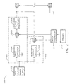
- a conventional stun gun 100 may be implemented according to the functional block diagram of FIG. 1 .
- closing safety switch S 1 connects a battery 102 to a microprocessor circuit 124 and places stun gun 100 in the "armed" and ready to fire configuration.
- Subsequent closure of trigger switch S2 causes microprocessor 124 to activate high voltage power supply 104.
- High voltage power supply 104 outputs a pulsed voltage of about 2,000 volts that is coupled to charge a capacitor 106 to the 2,000 volt power supply output voltage.
- the voltage across spark gap GAP 1 exceeds the ionization voltage of air, a relatively high voltage appears across the primary winding of transformer 108.
- Transformer 108 steps up this voltage to about 50,000 volts across the electrodes E1 and E2, ionizing the air in air gaps GAP A and GAP B at the target, modeled as a load having an impedance Z1. A relatively high voltage is thereby applied to load Z1. As the output voltage of capacitor 106 rapidly decreases, current flow through spark gap GAP 1 decreases, causing air in the spark gap to deionize and to resume an open circuit impedance. This "reopening" of spark gap GAP1 defines the end of each output pulse applied to electrodes E1 and E2. A typical stun gun of the type illustrated in FIG. 1 produces from five to twenty pulses per second.
- Taser International of Scottsdale, Arizona has for several years manufactured stun guns of the type illustrated in FIG. 1 and designated as the Taser® Model M18 and Model M26 stun guns.
- High power stun guns such as these typically incorporate an energy storage capacitor 106 having a capacitance of from about 0.2 to about 0.88 microfarads.
- targets that may be wearing clothing such as a leather or cloth jacket.
- Clothing functions to establish a gap of about 0.6 cm (0.25 inch) to about 2.5 cm (1 inch) between the target's skin and an electrode.
- An output voltage of about 50,000 volts will ionize an air gap of this length and support a current sufficient to induce muscular contractions in the target.
- high power stun guns such as the M18 and M26 stun guns
- the magnitude of the current flow across the spaced apart stun gun output electrodes may cause numerous groups of skeletal muscles to rigidly contract.
- the stun gun causes the target to lose its ability to maintain an erect, balanced posture. As a result, the target falls to the ground and is disabled.
- the air in one or both GAP A and GAP B between output electrodes E1 and E2 and the target ionizes and current begins flowing through electrodes E1 and E2.
- electrodes E1 and E2 are presented with a relatively low impedance load Z1 instead of the high impedance air gap or gaps, the stun gun output voltage will drop to a significantly lower voltage level.
- the output voltage of a model M26 stun gun might drop from about 55,000 volts to about 5,000 volts.
- Conventional stun guns have by necessity been designed to have the capability of causing ionization across one or more very high impedance air gaps at the target. As a result, such stun guns have been designed to produce an output from about 50,000 to about 60,000 volts. After ionization, the gap impedance is reduced to a very low level, yet the stun gun continues to operate in the same mode, delivering current or charge into a now very low impedance target. Consequently, the conventional high power, high voltage stun gun 100 discussed above operates relatively inefficiently, yielding a relatively low electro-muscular effect with relatively high battery power consumption.
- the M26 stun gun delivers about 26 watts of output power as measured at the capacitor 106. Due to inefficiencies of the high voltage power supply, the battery provides about 35 watts at a pulse rate of 15 pulses per second. Due to the requirement to generate a high voltage, high power ouput signal, the M26 stun gun requires a relatively large and relatively heavy eight AA cell battery pack 102. In addition, the M26 stun gun power generating solid state components 104, capacitor 106, step up transformer 108, and related parts on the primary side of transformer 108 must operate with relatively high current and high voltage (2,000 volts) and parts on the secondary side of transformer 108 must operate with repeated exposure to even higher voltage (50,000 volts).
- US 4,253,132 discloses a weapon for subduing and restraining including an electrically power supply.
- a manually operable launcher in combination with the power supply, is capable of delivering an electrical charge to a remote target via a projectile.
- the projectile is tethered to the launcher via a fine conducting fiber which can be coiled in the projectile.
- the present invention provides a device for disabling a target according to claim 1.
- the present invention provides a method for disabling a target according to claim 28.
- An electronic disabling device temporarily disables an animal or person (e.g., the target) and may to some extent immobilize and/or incapacitate the target while an electric current from the device is passing through the target.
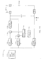
- the electronic disabling device 200 of FIG. 2 includes a power supply 202, first and second energy storage capacitors 204 and 210, and switches S 1 and S2 that each operate as SPST switches and serve to selectively connect the two energy storage capacitors to down stream circuit elements. Any number of physical capacitors in parallel or series connection may be used to implement a capacitor as discussed herein.
- the switches may be implemented in any conventional manner such as spark gaps and/or electronic switches (e.g., transistors).
- Capacitor 204 is selectively connected by switch S1 to a voltage multiplier 208 that is coupled to first and second electrodes E1 and E2. Electrodes may be fixed or implemented in darts as discussed above. Capacitors 204 and 210 are also coupled through a common conductor (circuit ground) to electrode E2.
- Trigger 216 e.g., a switch similar to a gun trigger
- switch controller 214 controls the timing and closure of switches S1 206 and S2 212.
- the output voltage V OUT across electrode E1 and E2 provided by operation of device 200 is the superposition of the voltage provided by each of two circuit portions 201 and 203.
- power supply 202 is activated at time T0 .
- Capacitors 204 and 210 charge during the time interval T0-T1.
- switch controller 214 closes switch S1 to couple capacitor 204 to voltage multiplier 208.
- FIG. 3 shows V OUT as a relatively high voltage during period T1 to T2.
- a high impedance air gap exists between electrode E1 and target contact point E3; and skin contact exists between electrode E2 and target contact point E4.
- Skin contact provides a low (e.g. near zero) impedance.
- Contact points E3 and E4 are spaced apart on the target as discussed above.
- the resistor and Z LOAD symbols represent the internal target resistance, typically less than 1,000 ohms, and may be about 200 ohms for a typical human target.
- switch controller 214 opens switch S1 and closes switch S2 to couple capacitor 210 to electrodes E1 and E2 as illustrated during period T2 to T3 of FIG. 4 .
- Capacitor 210 continues the ionization and maintains the arc across GAP A for a significant additional time interval.
- FIGs. 8 and 9 illustrate the voltage across electrodes for times T0 - T3.
- Switch controller 214 may be programmed to close switch S 1 for a predetermined period of time and then to close switch S2 for a predetermined period of time.
- interval T3 to T4 power supply 202 is disabled to maintain a factory preset pulse repetition rate.
- this factory preset pulse repetition rate defines the overall T0 to T4 time interval and its repetitions as in times T4 to T8 corresponding respectively to times T0 to T4.
- a timing control circuit implemented by a microprocessor maintains switches S 1 and S2 in the open condition during the T3 to T4 time interval and disables the power supply until the desired T0 to T4 time interval has been completed.
- the power supply will be reactivated to recharge capacitors 204 and 210 to the power supply output voltage.
- the duration of the interval T2 to T3 may be extended.
- electronic disabling device 1100 of FIG. 11 includes components described above and further includes third capacitor 1118 and diode D1.
- High voltage power supply 1102 charges capacitors 1110 and 1118 in parallel. While the second terminal of capacitor 1102 is connected to ground, the second terminal of capacitor 1118 is returned to ground through diode D1.
- FIG. 12 Another electronic disabling device 1200 of FIG. 12 is an implementation of the functions of device 1100 discussed above with reference to the functional block diagram of FIG. 11 .
- high voltage power supply 1202 provides two outputs of equal output voltage capability. Each output supplies a current: I1 to capacitors 1204 and 1218 (corresponding in function to first and third capacitors discussed above), and current I2 to capacitor 1210 (corresponding in function to the second capacitor discussed above).
- the first voltage output of high voltage power supply 1202 is also connected to GAP 1, a 2,000 volt spark gap; and to the primary winding of output transformer 1208 having a one to twenty-five primary to secondary winding step up ratio.
- the second terminal of capacitor 1210 is connected to ground while the second terminal of capacitor 1218 is returned to ground through resistor R1.
- the second voltage output of high voltage power supply 1202 is also connected to GAP2, a 3,000 volt spark gap.
- Spark gaps GAP1 and GAP2 are respectively in series with the primary and secondary windings of transformer 1208 having a 1 to 25 step up ratio.
- closure of safety switch S1 enables operation of high voltage power supply 1202 and places device 1200 in a standby/ready to operate configuration.
- Closure of trigger switch S2 causes microprocessor 1224 to assert an activate signal to high voltage power supply 1202.
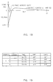
- power supply 1202 initiates current flow I1 charging capacitors 1204 and 1218 and current flow I2 charging capacitor 1210. This capacitor charging time interval will now be further described with reference to the voltage versus time graphs of FIGs. 13 through 18 .
- capacitors 1204 (C1), 1210 (C2), and 1218 (C3) charge from a zero voltage up to about 2,000 volts in response to outputs from high voltage power supply 1202. Spark gaps GAP1 and GAP2 remain open with near infinite impedance.
- the voltages of capacitors C1 and C3 approach the 2,000 volt breakdown rating of GAP1.
- an arc will be formed across GAP1 and the impedance of GAP 1 will drop to a near zero amount. This drop begins at time T1 in FIGs. 13-16 .
- capacitor C1 will begin discharging through the primary winding of transformer 1208.
- transformer 1208 By operation of transformer 1208, the voltage across electrodes E1 and E2 decreases rapidly to about -50,000 volts as shown in FIG. 16 .
- the voltage across capacitor C1 ( FIG. 15 ) decreases relatively slowly from about 2,000 volts while voltage across spark gap GAP2 increases relatively slowly toward the breakdown voltage of GAP2 ( FIG. 16 ).
- Device 1200 exhibits two modes of providing output signal V OUT across output electrodes E1 and E2.
- a relatively high voltage is supplied to ionize air in GAP A with energy supplied by capacitor C1 during time interval T1 to T2.
- a relatively lower voltage is supplied with energy supplied by capacitors C2 and C3 during time interval T2 to T3.
- device 1200 begins operating in the second mode of operation as spark gaps GAP2 and GAP A conduct at a low (near zero) impedance.
- the air in spark gaps GAP2 and GAP A is ionized at time T2 allowing capacitors C2 and C3 to discharge through electrodes E1 and E2 and the relatively low impedance load of the target.
- capacitor C 1 is discharging to a near zero amount as time approaches T2. Capacitor C1 does not discharge prior to time T2 because spark gap GAP2 is open. During the time interval T2 to T3, the voltage across capacitors C2 and C3 decreases to zero as these capacitors discharge through the now low impedance (target only) load seen across output terminals E1 and E2.
- FIG. 18 presents the voltage across GAP2 and the voltage across electrodes E1 and E2 during time interval T2 to T3. During most of the interval T2 to T3, the voltage across electrodes E1 and E2 has an absolute value less than about 2,000 volts.
- capacitor C 1 may provide about 0.14 microfarads and discharge during a time interval T1 to T2 of about 1.5 microseconds.
- Capacitors C2 and C3 may each provide about 0.02 microfarads and discharge during a time interval T2 to T3 of about 50 microseconds.
- durations are used for the duration of interval T1 to T2. This duration may be in the range from about 1.5 to about 0.5 microseconds.
- durations are used for the duration of interval T2 to T3. This duration may be in the range from about 20 to about 200 microseconds.
- interval T0 to T1 depends on the ability of power supply 1201 to supply current sufficient operate device 1200 while charging capacitors C1, C2, and C3. For example, a fresh battery 1201 may shorten the T0 to T1 time interval in comparison to circuit operation with a partially discharged battery. Operation of device 1200 in cold ambient temperature may degrade battery capacity and may also increase the duration of interval T0 to T1.
- controller 1214 includes a conventional microprocessor circuit programmed to perform methods according to various aspects of the present invention. According to various aspects of the present invention, controller 1214 provides the activate signal to high voltage power supply 1202 in accordance with a feedback signal to control the duration of digital pulse control intervals ( FIG. 10 ) and consequently cycle durations (TA and TB of FIG. 10 ). Digital pulse control intervals correspond to interval T3 to T4 discussed above.
- controller 12 14 of FIG. 12 includes microprocessor 1224 and feedback signal conditioning circuit 1222.
- Microprocessor 1224 receives a feedback signal from high voltage power supply 1202 via feedback signal conditioning circuit 1222.
- Feedback signal conditioning circuit provides to microprocessor 1224 a status signal in response to the feedback signal.
- Microprocessor 1224 detects when time T3 has been reached as illustrated in FIGs. 4 , 7 , 8 , 9 , 10 , 17 and 18 . Since the commencement time T0 of the operating cycle is known, the microprocessor will maintain the high voltage power supply in a shut down or disabled operating mode from time T3 until a time sufficient to implement the preset pulse repetition rate (e.g., interval T3 to T4). While the duration of interval T3 to T4 may vary to compensate for other intervals, the microprocessor maintains the T0 to T4 time interval to accomplish the preset pulse repetition rate.
- FIG. 19 table entitled “Gap On/Off Timing” represents a simplified summary of the configuration of GAP 1 and GAP2 during the four relevant operating time intervals.
- the configuration "off” represents the high impedance, non-ionized spark gap state while the configuration "on” represents the ionized state where the spark gap breakdown voltage has been reached.
- the voltages within the device are reduced to facilitate the design of a compact electronic disabling device using conventional insulating materials.
- an implementation may use a voltage multiplier having dual outputs each providing half the output voltage.
- the voltage across electrodes E1 and E2 may then be the sum of the dual output voltages.
- voltage multiplier circuit 2000 of FIG. 20 includes transformer 1008 having a single primary winding and a center-tapped or two separate secondary windings.
- the step up ratio from the primary winding to each secondary winding is 1 to 12.5.
- Transformer 1208 still accomplishes the objective of achieving a 25 to 1 step-up ratio for generating an output signal of about 50,000 volts from about a 2,000 volt power supply.
- This double secondary transformer configuration is that the maximum voltage applied to each secondary winding is reduced by 50% in comparison to designs using one secondary winding. Such reduced secondary winding operating potentials may be desired to achieve a higher output voltage with a given amount of transformer insulation or for placing less high voltage stress on the elements of the output transformer.
- the M26 stun gun utilizes a single energy storage capacitor of about 0.88 microfarads. When charged to 2,000 volts, that capacitor stores and subsequently discharges about 1.76 joules of energy during each output pulse. For a standard pulse repetition rate of 15 pulses per second and 1.76 joules per pulse, the M26 stun gun requires about 35 watts of input power which, as explained above, must be provided by a large, relatively heavy battery power supply utilizing 8 series-connected AA alkaline battery cells.
- An electronic disabling device may use capacitors having capacitance as follows: C1 about 0.07 microfarads and C2 about 0.01 microfarads. The sum of capacitance for C1 and C2 is about 0.08 microfarads.
- An electronic disabling device 200 using these values for C 1 and C2 provides each output pulse from about 0.16 joules of energy stored on these capacitors. With a pulse repetition rate of about 15 pulses per second, these two capacitors consume battery power of about 2.4 watts at the capacitors and roughly 3.5 to 4 watts at the battery. As a result, the battery may be a single AA size battery. This electronic disabling device achieves a 90% reduction in power consumption compared to the M26 stun gun, discussed above.
- An electronic disabling device generates a time-sequenced, shaped, voltage output waveform as illustrated in FIGs. 3 and 4 .
- the output waveform accommodates two different load configurations presented: a relatively high voltage output operating mode during the high impedance T1 to T2 first operating interval and, a relatively low voltage output operating mode during the low impedance second T2 to T3 operating interval.
- the circuit elements operate at lower power levels and lower voltage levels resulting in more reliable circuit operation. Further, such electronic disabling devices may be packaged in a much more physically compact design.
- the prototype size in comparison to the size of an M26 stun gun is reduced by approximately 50% and the weight is reduced by approximately 60%.
- battery capacity is predicted by the controller. Further, a readout of battery capacity may be provided to the user. In most electronic devices the remaining battery capacity can be predicted either by measuring the battery voltage during operation or integrating the battery discharge current over time. Due to the several modes of operation discussed above, prior art battery management methods yield unreliable results. Since ambient temperature strongly affects battery capacity and operation of electronic disabling devices is desired in a wide range of ambient temperatures, non-temperature compensated prior art battery capacity prediction methods produce even less reliable results.
- the battery power consumption of an electronic disabling device varies with operating mode as follows.
- the device includes a real time clock, a laser, and a flashlight in addition to elements discussed above.
- the real time clock may draw about 3.5 microamps. If the system safety switch S 1 is armed, the now-activated the microprocessor and its clock may draw about 4 milliamps. If enabled, and if the safety switch is armed, the laser target designator may draw about 11 milliamps. If enabled, and if the safety switch is armed, the forward facing low intensity twin white LED flashlight may draw about 63 milliamps. If the safety switch is armed and the trigger switch S2 is pulled, the device will draw from about 3 to about 4 amps. Therefore, the minimum to maximum current drain will vary in a ratio of about 1,000,000 to 1.
- the capacity of lithium batteries packaged in the system battery module may vary greatly over the operating temperature range.
- the battery module may deliver about 100 5-second discharge cycles.
- the battery module may deliver about 350 5-second discharge cycles.
- battery life varies from about 5,000,000 to 1.
- a battery capacity assessment system predicts the remaining battery capacity based on laboratory measurements of critical battery parameters under different loads and at different temperature conditions. These measured battery capacity parameters are stored electronically as a table (e.g., columns 1 and 2 of FIG. 25 ) in an electronic non-volatile memory device included with each battery module. ( FIG. 22 ) As illustrated in FIGs. 21 and 22 , appropriate data interface contacts enable the microprocessor to communicate with the table electronically stored in the battery module 2200 to predict remaining capacity of the battery (2202 and 2204).
- the battery module 2200 with internal electronic non-volatile memory may be referred to as the Digital Power Magazine (DPM) or simply as the system battery module.
- DPM Digital Power Magazine
- the data required to construct the data tables for the battery module were collected by operating the electronic disabling device at selected temperatures while recording the battery performance and longevity at each temperature interval.
- the resulting battery capacity measurements were collected and organized into a tabular spreadsheet of the type illustrated in FIG. 25 .
- the battery drain parameters for each system feature were calculated and translated into standardized drain values in microamp-hours ( ⁇ AH) based on the sensible operating condition of that feature.
- ⁇ AH microamp-hours
- the battery drain required to keep the clock alive is represented by a number in ⁇ AH that totals the current required to keep the clock alive for about 24 hours.
- the battery drain to power up the microprocessor, the forward directed flashlight, and the laser target designator for one second are represented by separate table entries with values in ⁇ AH.
- the battery drain required to operate the gun in the firing mode is represented by numbers in ⁇ AH of battery drain required to fire a single power output pulse.
- the total available battery capacity at each incremental temperature was measured.
- the battery capacity in ⁇ AH at 25°C (ambient) was programmed into the table to represent a normalized one hundred percent battery capacity value.
- the battery table drain numbers at other temperatures were adjusted to coordinate with the 25°C total (one hundred percent) battery capacity number. For example, since the total battery capacity at -20°C was measured to approximate 35% of the battery capacity at 25°C, the ⁇ AH numbers at -20°C were multiplied by 1/0.35.
- An additional location in the memory for the table discussed above (not shown in FIG. 25 ) is used by the microprocessor to keep track of used battery capacity.
- This number i.e., used battery capacity
- This number is updated about every one second if the safety selector remains in the "armed” position, and about every twenty-four hours if the safety selector remains in the "safe” position.
- Remaining battery capacity percentage is calculated by dividing this number by the total battery capacity.
- the device displays this percent of battery capacity remaining on a two digit Central Information Display (CID) for two seconds each time the device is armed.
- CID Central Information Display
- device 2300 is referred to as the model X26.
- Figure 22 illustrates the electronic circuit located inside the X26 battery module.
- the removable battery module consists of two series-connected, 3-volt CR123 lithium batteries and a nonvolatile memory device.
- the nonvolatile memory device may take the form of a 24AA128 flash memory which contains 128K bits of data storage.
- the electrical and data interface between the X26 system microprocessor and battery module is established by a 6-pin jack JP1 and provides a 2-line I 2 C serial bus for data transmission purposes.
- a cell phone selectively operates in the following different power consumption modes: (1) power off/microprocessor clock on; (2) power on, standby/receive mode; (3) receiving an incoming telephone call and amplifying the received audio input signal; (4) transmit mode generating an RF power output of about 600 milliwatts; (5) ring signal activated in response to an incoming call; and (6) backlight on.
- a battery module analogous to that illustrated in the FIG. 22 electrical schematic diagram would be provided. That module would include a memory storage device such as the element designated by reference number U1 in the FIG. 22 schematic diagram to receive and store a battery consumption table of the type discussed above with reference to FIG. 25 .
- the cell phone microprocessor can then be programmed to read out and display either at power up or in response to a user-selectable request the battery capacity remaining within the battery module or the percent of used capacity.
- the battery capacity table would be calibrated for each different power consumption mode based on the power consumption of each individual operating element. Battery capacity would also be quantified for a specified number of different ambient temperature operating ranges.
- An X26 system embodiment of the present invention is shipped from the factory with an internal battery module (DPM) having sufficient battery capacity to energize the internal clock for much longer than 10 years.
- the internal clock is set at the factory to Greenwich Mean Time (GMT).
- GTT Greenwich Mean Time
- the internal X26 system electronic warranty tracker begins to count down the factory preset warranty period or duration beginning with the first trigger pull occurring about 24 hours or more after the X26 system has been packaged for shipment by the factory.
- the X26 system Whenever the battery module is removed from the X26 system and replaced one or more seconds later, the X26 system will implement an initialization procedure.
- the 2-digit LED Central Information Display (CID), sequentially reads out a series of 2-digit numbers which represent the following data: (1) The first 3 sets of 2-digit numbers represent the warranty expiration date in the format YY/MM/DD; (2) The current date is displayed: YY/MM/DD; (3) The internal temperature in degrees Centigrade is displayed: XX (negative numbers are represented by blinking the number); and (4) The software revision is displayed: XX.
- CID Central Information Display
- the system warranty can be extended by communication via the Internet or by purchase of a replacement battery module.
- the X26 system includes a USB data interface module accessory which is physically compatible with the shape of the X26 system receptacle for battery module 12.
- the USB data module can be inserted within the X26 system battery module receptacle and includes a set of electrical contacts compatible with jack JP1 located inside the X26 system battery module housing.
- the USB interface module may be electrically connected to a computer USB port which supplies power via jack JP1 to the X26 system. While the USB interface is normally used to download firing data from the X26 system, it can also be used to extend the warranty period or to download new software into the X26 microprocessor system.
- the user removes the X26 battery module, inserts the USB module, connects a USB cable to an Internet enabled computer, goes to the www.Taser.com website, follows the download X26 system warranty extension instructions, and pays for the desired extended warranty period by credit card.
- the system warranty can also be extended by purchasing from the factory a specially programmed battery module having the software and data required to reprogram the warranty expiration data stored in the X26 microprocessor.
- the warranty extension battery module is inserted into the X26 system battery receptacle. If the X26 system warranty period has not yet expired, the data transferred to the X26 microprocessor will extend the current warranty expiration date by the period pre-programmed into the extended warranty battery module. Once the extended warranty expiration date has been stored within the X26 system, the microprocessor will initiate a battery insertion initialization sequence and will then display the new warranty expiration date.
- warranty extension modules can be provided to either extend the warranty of only a single X26 system or to provide warranty extensions for multiple system as might be required to extend the warranty for X26 systems used by an entire police department. If the warranty extension module contains only one warranty extension, the X26 microprocessor will reset the warranty update data in the module to zero.
- the module can function either before or after the warranty extension operation as a standard battery module.
- An X26 system may be programmed to accept one warranty extension, for example a one year extension, each time that the warranty extension module is inserted into the weapon.
- the warranty configuration/warranty extension feature of the present invention could also readily be adapted for use with any microprocessor-based electronic device or system having a removable battery.
- a circuit similar to that illustrated in the FIG. 22 electrical schematic diagram could be provided in the cell phone battery module to interface with the cellular phone microprocessor system.
- the cell phone would be originally programmed at the factory to reflect a device warranty of predetermined duration at the initial time that the cell phone was powered up by the ultimate user/customer.
- a customer could readily replace the cell phone battery while simultaneously updating the system warranty.
- a purchaser of an electronic device incorporating the warranty extension feature of the present invention could return to a retail outlet, such as Best Buy or Circuit City, purchase a warranty extension and have the on-board system warranty extended by a representative at that retail vendor.
- This warranty extension could be implemented by temporarily inserting a master battery module incorporating a specified number of warranty extensions purchased by the retail vendor from the OEM manufacturer.
- the retail vendor could attach a USB interface module to the customer's cell phone and either provide a warranty extension directly from the vendor's computer system or by means of data supplied by the OEM manufacturer's website.
- warranty extension feature of the present invention could be provided to extend the warranty of other devices such as desktop computer systems, computer monitors or even an automobile.
- either the OEM manufacturer or a retail vendor could supply to the customer's desktop computer, monitor or automobile with appropriate warranty extension data in exchange for an appropriate fee.
- Such data could be provided to the warranted product via direct interface with the customer's product by means of an infrared data communication port, by a hard-wired USB data link, by an IEEE 1394 data interface port, by a wireless protocol such as Bluetooth or by any other means of exchanging warranty extension data between a product and a source of warranty extension data.
- the X26 system can be supplied with firmware updates by the battery module.
- the X26 system microcontroller will read several identification bytes of data from the battery module. After reading the software configuration and hardware compatibility table bytes of the new program stored in the nonvolatile memory within the battery module to evaluate hardware/software compatibility and software version number, a system software update will take place when appropriate.
- the system firmware update process is implemented by having the microprocessor (see FIG. 21 ) in the X26 system read the bytes in the battery module memory program section and programming the appropriate software into the X26 system nonvolatile program memory.
- the X26 system can also receive program updates through a USB interface module by connecting the USB module to a computer to download the new program to a nonvolatile memory provided within the USB module.
- the USB module is next inserted into the X26 system battery receptacle.
- the X26 system will recognize the USB module as providing a USB reprogramming function and will implement the same sequence as described above in connection with X26 system reprogramming via battery module.
- the High Voltage Assembly (HVA) schematically illustrated in FIGS. 23 and 24 provides an output of about 50,000 from an input of from about 3 to about 6 volts.
- HVA High Voltage Assembly
- the microprocessor To enable the HVA, the microprocessor must output a 500 Hz square wave with an amplitude of from about 2.5 to about 6 volts and a duty cycle of about 50%.
- the D6 series diode within the HVA power supply "rectifies” the ENABLE signal and uses it to charge up capacitor C6.
- the voltage across capacitor C6 is used to run pulse width modulation (PWM) controller U1 in the HVA.
- PWM pulse width modulation
- resistor R3 charges capacitor C8. If the charge level on C8 goes above about 1.23 volts, the PWM will shut down -- stopping delivery of 50,000 volt output pulses. Every time the ENABLE signal goes low, capacitor C8 is discharged, making sure the PWM can stay “on” as the ENABLE signal goes back high and starts charging C8 again. Any time the ENABLE signal remains high for more than about 1 millisecond, the PWM controller will be shut down.
- the configuration of the X26 system high voltage output circuit represents a key distinction between the X26 system and conventional prior art stun guns.
- the switch mode power supply will charge up capacitors C1, C2, and C3 through diodes D1, D2, and D3.
- diodes D1 and D2 can be connected to the same or to different windings of 2301 (T1) to modify the output waveform.
- the ratios of the T1 primary and secondary windings and the spark gap voltages on GAP1, GAP2, and GAP3 are configured so that GAP1 will always breakdown and fire first.
- spark coil transformer 2305 When GAP1 fires, 2,000 volts is applied across the primary windings of spark coil transformer 2305 (T2) from pin 6 to pin 5.
- the secondary voltage on spark coil transformer T2 from pins 1 to 2 and from pins 3 to 4 will approximate 25,000 volts, depending on the air gap spacing between the two output electrodes E1 and E2. The smaller the air gap, the smaller the output voltage before the air gap across output terminals E1 to E2 breaks down, effectively clamping the output voltage level.
- the voltage induced in the secondary current path by the discharge of C 1 through GAP1 and T2 sets up a voltage across C2, GAP2, E1 to E2, GAP3, C3 and C1.
- the cumulative voltage across the air gaps GAP2, E1 to E2, and GAP3
- current will start flowing in the circuit, from C2 through GAP2, through the output electrodes E1 to E2, through GAP3, and through C3 in series with C1 back to ground.
- C1 is driving the output current through GAP1 and T2
- the output current as described will remain negative in polarity.
- the charge level stored in both C2 and C3 will increase.
- T1 will not be able to maintain the output voltage across the output windings (from pin 1 to pin 2, and from pin 3 to pin 4). At that time, the output current will reverse and begin flowing in a positive direction and will begin depleting the charge on C2 and C3.
- the discharge of C1 is known as the "arc" phase.
- the discharge of C2 and C3 is known as the muscle "stimulation" phase.
- the high voltage output coil T2 as illustrated in FIG. 24 consists of two separate secondary windings that create a negative polarity spark voltage on E1 followed by a positive polarity spark voltage on E2, the peak voltage measured from either electrode E1 or E2 to primary weapon ground will not exceed about 25,000 volts yet the peak voltage measured across power supply output terminals E1 and E2 will reach about 50,000 volts. If the output coil T2 had utilized only a single secondary winding as is the case with all prior art stun guns and in other embodiments of the present invention, the maximum voltage from one output electrode (E1 or E2) referenced to primary weapon ground would reach about 50,000 volts.
- a feedback signal from the primary side of the HVA provides a mechanism for the FIG. 21 microprocessor to indirectly determine the voltage on capacitor C1, and hence where the X26 system power supply is operating within its pulse firing sequence. This feedback signal is used by the microprocessor to control the output pulse repetition rate.
- the system pulse rate may be controlled to create either a constant or a time-varying pulse rate by having the microcontroller stop toggling the ENABLE signal for short time periods, thereby holding back the pulse rate to reach a preset, lower value.
- the preset values may be changed based on the length of the pulse train. For example, in a police model, the system may be preprogrammed such that a single trigger pull will produce a 5-second long power supply activation period. For the first 2 seconds of that 5-second period, the microprocessor may be programmed to control (pull back) the pulse rate to about 19 pulses per second (PPS), while for the last 3 seconds of the 5-second period, the pulse rate could be programmed to be reduced to about 15 PPS.
- PPS pulses per second
- the X26 system may be programmed to continue discharging at 15 PPS for as long as the trigger is held down.
- the X26 system could alternatively be programmed to produce various different pulse repetition rate configurations such as, for example: 0-2 seconds : 17 PPS, 2-5 seconds : 12 PPS, 5-6 seconds : 0.1 PPS, 6-12 seconds : 11 PPS, 12-13 seconds : 0.1 PPS, 13-18 seconds : 10 PPS, 18-19 seconds : 0.1 PPS, 18-23 seconds : 9 PPS.
- pulse repetition rate configurations could be applied to a civilian version of the X26 system where longer activation periods are desirable.
- lowering the pulse rate will reduce battery power consumption, extend battery life, and potentially enhance the medical safety factor.
- the operating cycle of the HVA can be divided into the following 4 time periods as illustrated in FIG. 26.
- capacitors C1, C2 and C3 are charged by one, two, or three power supplies to the breakdown voltage of spark gap GAP 1.
- GAP1 has switched ON, allowing C1 to pass a current through the primary winding of the high voltage spark transformer T2 which causes the secondary voltage (across E1 to E2) to increase rapidly.
- the high output voltage caused by the discharge of C1 through the primary transformer winding will cause voltage breakdown across GAP2, across E1 to E2, and across GAP3.
- the microprocessor measured the time required to generate a single shaped waveform output pulse.
- the desired pulse repetition rate was pre-programmed into the microprocessor.
- the microprocessor will temporarily shut down the power supply for a period required to achieve the preset pulse repetition rate. Because the microprocessor is inserting a variable length T3 to T4 shut-off period, the system pulse repetition rate will remain constant independent of battery voltage and circuit component variations (tolerance).
- the microprocessor-controlled pulse rate methodology allows the pulse rate to be software controlled to meet different customer requirements.
- the FIG. 10 timing diagram shows an initial fixed timing cycle TA followed by a subsequent, longer duration timing cycle TB.
- the shorter timing cycle followed by the longer timing cycle reflects a reduction in the pulse rate.
- the X26 system can vary the pulse rate digitally during a fixed duration operating cycle. As an example, a pulse rate of about 19 PPS may be achieved for about 2 seconds of initial operation and then reduced to about 15 PPS for about 3 seconds, further reduced to about 0.1 PPS for about 1 second, and then increased to about 14 PPS for about 5 seconds.
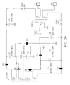
- FIGs. 23A and 23B utilizes three spark gaps.
- GAP1 requires a precise breakdown voltage rating, in this case about 2,000 volts.
- GAP2 and GAP3 only require a breakdown voltage rating significantly higher than the voltage stress induced on them during the time interval before GAP1 breaks down.
- GAP2 and GAP3 have been provided solely to ensure that if a significant target skin resistance is encountered during the initial current discharge into the target that the muscle activation capacitors C2 and C3 will not discharge before GAP1 breaks down. To perform this optional, enhanced function, only one of these secondary spark gaps (either GAP2 or GAP3) need be provided.
- FIG. 24 illustrates a high voltage section with significantly improved efficiency.
- transformer T1 has been reconfigured to provide 3 series-connected secondary windings where the design output voltage of each winding has been limited to about 1,000 volts.
- capacitor C1 is charged to about 2,000 volts by transformer winding and diode D1.
- C 1 is charged by combining the voltages across C5 and C6.
- Each T1 transformer winding coupled to charge C5 and C6 is designed to charge each capacitor to about 1,000 volts, rather than to 2,000 volts as in the FIG. 23B circuit.
- the losses due to parasitic circuit capacitances are a function of the transformer AC output voltage squared, the losses due to parasitic circuit capacitances with the FIG. 24 1,000 volt output voltage compared to the FIG. 23B 2,000 volt transformer output voltage are reduced by a factor of 4.
- the current required to charge C2 is derived in part from capacitor C6, the positive side of which is charged to about 2,000 volts.
- the voltage across the transformer winding is reduced to about 1,000 volts in comparison to the 3,000 volts produced across the corresponding transformer T1 winding in the FIG. 23B circuit.
- FIG. 23B and FIG. 24 circuit designs relate to the interaction of C1 to C3.
- the charge on C1 is about 2,000 volts while the charge on C3 is about 3,000 volts.
- the voltage across C3 remains at about 3,000 volts.
- the positive side of C3 is now at ground level, the negative terminal of C3 will be at about -3,000 volts.
- a differential voltage of about 6,000 volts has been created between the positive terminal of C2 and the negative terminal of C3,
- the T2 output windings merely act as conductors.
- the X26 system trigger position is read by the microprocessor which may be programmed to extend the duration of the operating cycle in response to additional trigger pulls. Each time the trigger is pulled, the microprocessor senses that event and activates a fixed time period operating cycle. After the gun has been activated, the Central Information Display (CID) on the back of the X26 handle indicates how much longer the X26 system will remain activated.
- the X26 system activation period may be preset to yield a fixed operating time, for example, about 5 seconds. Alternatively, the activation period may be programmed to be extended in increments in response to additional, sequential trigger pulls. Each time the trigger is pulled, the CID readout will update the countdown timer to the new, longer timeout.
- the incrementing trigger feature will allow a civilian who uses the X26 system on an aggressive attacker to initiate multiple trigger pulls to activate the gun for a prolonged period, enabling the user to lay the gun down on the ground and get away.
- the X26 system may provide an internal non-volatile memory set aside for logging the time, duration of discharge, internal temperature and battery level each time the weapon is fired.
- the stun gun clock time always remains set to GMT.
- a translation from GMT to local time may be provided.
- both GMT and local time may be shown.
Description
- The present invention relates to devices for disabling an animal or human target; and to methods for providing an electric current through electrodes and the target in a circuit having an air gap between an electrode and the target.
- The original stun gun was invented in the 1960's by Jack Cover. Such prior art stun guns incapacitated a target by delivering a sequence of high voltage pulses into the skin of the target such that the current flow through the target interferes with the target's neuromuscular system. Lower power systems cause a stun effect. Higher power systems cause involuntary muscle contractions. Electronic disabling devices, such as stun guns, have been made in two designs. A first design has electrodes fixed to the gun. In operation the user establishes direct contact of the electrodes to the target. A second design operates on a remote target by launching a pair of darts. Each dart includes an electrode that typically includes a barbed point. The darts either engage the clothing worn by the target or engage the target's skin. In most cases, a high impedance air gap exists between one or both of the electrodes and the skin of the target because one or both of the electrodes contact the target's clothing rather than penetrating the target's skin.
- A
conventional stun gun 100 may be implemented according to the functional block diagram ofFIG. 1 . Instun gun 100, closingsafety switch S 1 connects abattery 102 to amicroprocessor circuit 124 and placesstun gun 100 in the "armed" and ready to fire configuration. Subsequent closure of trigger switch S2 causesmicroprocessor 124 to activate highvoltage power supply 104. Highvoltage power supply 104 outputs a pulsed voltage of about 2,000 volts that is coupled to charge acapacitor 106 to the 2,000 volt power supply output voltage. When the voltage acrossspark gap GAP 1 exceeds the ionization voltage of air, a relatively high voltage appears across the primary winding oftransformer 108.Transformer 108 steps up this voltage to about 50,000 volts across the electrodes E1 and E2, ionizing the air in air gaps GAPA and GAPB at the target, modeled as a load having an impedance Z1. A relatively high voltage is thereby applied to load Z1. As the output voltage ofcapacitor 106 rapidly decreases, current flow throughspark gap GAP 1 decreases, causing air in the spark gap to deionize and to resume an open circuit impedance. This "reopening" of spark gap GAP1 defines the end of each output pulse applied to electrodes E1 and E2. A typical stun gun of the type illustrated inFIG. 1 produces from five to twenty pulses per second. - Taser International of Scottsdale, Arizona, has for several years manufactured stun guns of the type illustrated in
FIG. 1 and designated as the Taser® Model M18 and Model M26 stun guns. High power stun guns such as these typically incorporate anenergy storage capacitor 106 having a capacitance of from about 0.2 to about 0.88 microfarads. - It is desirable to disable targets that may be wearing clothing such as a leather or cloth jacket. Clothing functions to establish a gap of about 0.6 cm (0.25 inch) to about 2.5 cm (1 inch) between the target's skin and an electrode. An output voltage of about 50,000 volts will ionize an air gap of this length and support a current sufficient to induce muscular contractions in the target. With high power stun guns, such as the M18 and M26 stun guns, the magnitude of the current flow across the spaced apart stun gun output electrodes may cause numerous groups of skeletal muscles to rigidly contract. For a human target, the stun gun causes the target to lose its ability to maintain an erect, balanced posture. As a result, the target falls to the ground and is disabled.
- At about 50,000 volts, the air in one or both GAPA and GAPB between output electrodes E1 and E2 and the target ionizes and current begins flowing through electrodes E1 and E2. When electrodes E1 and E2 are presented with a relatively low impedance load Z1 instead of the high impedance air gap or gaps, the stun gun output voltage will drop to a significantly lower voltage level. For example, with a human target and with about probe to probe separation of about 25 cm (10 inches), the output voltage of a model M26 stun gun might drop from about 55,000 volts to about 5,000 volts. Conventional stun guns exhibit this rapid voltage drop because such stun guns are tuned to operate in only a single mode to consistently create an electrical arc across a very high, near infinite impedance air gap. After a low impedance circuit is formed through the electrodes and air gap or gaps at the target, the effective stun gun load impedance decreases toward the target's impedance, generally about 1,000 ohms or less. A typical human subject may present a load impedance of about 200 ohms.
- Conventional stun guns have by necessity been designed to have the capability of causing ionization across one or more very high impedance air gaps at the target. As a result, such stun guns have been designed to produce an output from about 50,000 to about 60,000 volts. After ionization, the gap impedance is reduced to a very low level, yet the stun gun continues to operate in the same mode, delivering current or charge into a now very low impedance target. Consequently, the conventional high power, high
voltage stun gun 100 discussed above operates relatively inefficiently, yielding a relatively low electro-muscular effect with relatively high battery power consumption. - The M26 stun gun delivers about 26 watts of output power as measured at the
capacitor 106. Due to inefficiencies of the high voltage power supply, the battery provides about 35 watts at a pulse rate of 15 pulses per second. Due to the requirement to generate a high voltage, high power ouput signal, the M26 stun gun requires a relatively large and relatively heavy eight AAcell battery pack 102. In addition, the M26 stun gun power generatingsolid state components 104,capacitor 106, step uptransformer 108, and related parts on the primary side oftransformer 108 must operate with relatively high current and high voltage (2,000 volts) and parts on the secondary side oftransformer 108 must operate with repeated exposure to even higher voltage (50,000 volts). - Without devices and methods of the present invention, the cost of manufacturing and operating electronic disabling devices will restrict widespread use of these weapons for law enforcement and personal safety.
-
US 4,253,132 discloses a weapon for subduing and restraining including an electrically power supply. A manually operable launcher, in combination with the power supply, is capable of delivering an electrical charge to a remote target via a projectile. The projectile is tethered to the launcher via a fine conducting fiber which can be coiled in the projectile. - In a first aspect the present invention provides a device for disabling a target according to
claim 1. - In a second aspect the present invention provides a method for disabling a target according to claim 28.
- Systems and methods of the present invention will be described with reference to the drawing wherein like numbers denote like elements, and;
-
FIG. 1 is a functional block diagram of a stun gun of the prior art; -
FIG. 2 is a functional block diagram of an electronic disabling device according to various aspects of the present invention; -
FIG. 3 is a graph illustrating a generalized output voltage waveform of thecircuit portion 201 ofFIG. 2 ; -
FIG. 4 is a graph illustrating a generalized output voltage waveform of thecircuit portio 203 ofFIG. 2 ; -
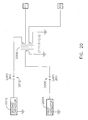
FIG. 5 illustrates a high impedance air gap which may exist between one of the electronic disabling device output electrodes E1 and a spaced apart location E3 on a target; -
FIG. 6 illustrates the air gap ofFIG. 5 after ionization; -
FIG. 7 is a graph illustrating the impedance of air gap GAPA ofFIG. 5 during time periods ofFIGs. 3 and 4 ; -
FIG. 8 is a graph of voltage versus time for the device ofFIG. 2 ; -
FIG. 9 is a graph of voltage versus time for the device ofFIG. 2 ; -
FIG. 10 is a graph of time for the sequence of two output pulses ofFIG. 9 ; -
FIG. 11 is a functional block diagram of another electronic disabling device according to various aspects of the present invention; -
FIG. 12 is a functional block diagram of yet another electronic disabling device according to various aspects of the present invention; -
FIGs. 13-18 are timing diagrams illustrating the voltages across capacitors C1, C2, and C3 ofFIG. 12 during times TO-T3; -
FIG. 19 is a table indicating the effective impedance of GAP1 and GAP2 during time intervals ofFIGs. 13-18 ; -
FIG. 20 is a functional block diagram of an alternative implementation ofcircuit portions FIG. 2 ; -
FIG. 21 is a schematic diagram ofcontroller 1214 ofFIG. 12 ; -
FIG. 22 is a schematic diagram ofpower supply 1201 ofFIG. 12 ; -
FIGs. 23A and23B form a schematic diagram of another portion of circuitry of the device ofFIG. 12 ; -
FIG. 24 is a schematic diagram of an alternative circuit for the circuit ofFIG. 23B ; and -
FIG. 25 is a batter power consumption table. - An electronic disabling device, according to various aspects of the present invention, temporarily disables an animal or person (e.g., the target) and may to some extent immobilize and/or incapacitate the target while an electric current from the device is passing through the target. For example, the electronic disabling
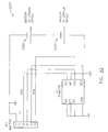
device 200 ofFIG. 2 includes apower supply 202, first and secondenergy storage capacitors S 1 and S2 that each operate as SPST switches and serve to selectively connect the two energy storage capacitors to down stream circuit elements. Any number of physical capacitors in parallel or series connection may be used to implement a capacitor as discussed herein. The switches may be implemented in any conventional manner such as spark gaps and/or electronic switches (e.g., transistors).Capacitor 204 is selectively connected by switch S1 to avoltage multiplier 208 that is coupled to first and second electrodes E1 and E2. Electrodes may be fixed or implemented in darts as discussed above.Capacitors - Trigger 216 (e.g., a switch similar to a gun trigger) controls
switch controller 214 that controls the timing and closure ofswitches S1 206 andS2 212. - The output voltage VOUT across electrode E1 and E2 provided by operation of
device 200 is the superposition of the voltage provided by each of twocircuit portions operation power supply 202 is activated at time T0 .Capacitors FIG. 3 ,switch controller 214 closes switch S1 to couplecapacitor 204 tovoltage multiplier 208.FIG. 3 shows VOUT as a relatively high voltage during period T1 to T2. - In the hypothetical situation illustrated in
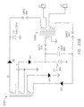
FIG. 5 , a high impedance air gap exists between electrode E1 and target contact point E3; and skin contact exists between electrode E2 and target contact point E4. Skin contact provides a low (e.g. near zero) impedance. Contact points E3 and E4 are spaced apart on the target as discussed above. The resistor and ZLOAD symbols represent the internal target resistance, typically less than 1,000 ohms, and may be about 200 ohms for a typical human target. - Application of the VHIGH voltage across the E1 to E3 gap GAPA ionizes the air in the gap to form an arc. Consequently, the impedance of GAPA drops from a near infinite amount to a near zero amount as in
FIG. 7 , producing the circuit configuration as inFIG. 6 . After this low impedance ionized path from E1 to E3 has been established by the short duration application of the VHIGH output signal,switch controller 214 opens switch S1 and closes switch S2 to couplecapacitor 210 to electrodes E1 and E2 as illustrated during period T2 to T3 ofFIG. 4 .Capacitor 210 continues the ionization and maintains the arc across GAPA for a significant additional time interval. This continuing, lower voltage discharge of thecapacitor 210 during the interval T2 to T3 transfers a substantial amount of electrical charge through the target to disable the target. The continuing discharge ofcapacitor 210 through the target will eventually exhaust the charge stored incapacitor 210 and will ultimately cause the output voltage to drop to a voltage at which ionization is no longer supported in GAPA. GAPA will then revert to the non-ionized, high impedance state causing cessation of current flow through the target.FIGs. 8 and9 illustrate the voltage across electrodes for times T0 - T3. -
Switch controller 214 may be programmed to closeswitch S 1 for a predetermined period of time and then to close switch S2 for a predetermined period of time. - During interval T3 to T4,
power supply 202 is disabled to maintain a factory preset pulse repetition rate. As illustrated in the timing diagrams ofFIGs. 9 and10 , this factory preset pulse repetition rate defines the overall T0 to T4 time interval and its repetitions as in times T4 to T8 corresponding respectively to times T0 to T4. A timing control circuit implemented by a microprocessor maintainsswitches S 1 and S2 in the open condition during the T3 to T4 time interval and disables the power supply until the desired T0 to T4 time interval has been completed. At time T4, the power supply will be reactivated to rechargecapacitors - In an alternate implementation, the duration of the interval T2 to T3 may be extended. For example, electronic disabling
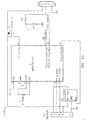
device 1100 ofFIG. 11 includes components described above and further includesthird capacitor 1118 and diode D1. Highvoltage power supply 1102charges capacitors capacitor 1102 is connected to ground, the second terminal ofcapacitor 1118 is returned to ground through diode D1. - Another electronic disabling
device 1200 ofFIG. 12 is an implementation of the functions ofdevice 1100 discussed above with reference to the functional block diagram ofFIG. 11 . Indevice 1200, highvoltage power supply 1202 provides two outputs of equal output voltage capability. Each output supplies a current: I1 tocapacitors 1204 and 1218 (corresponding in function to first and third capacitors discussed above), and current I2 to capacitor 1210 (corresponding in function to the second capacitor discussed above). The first voltage output of highvoltage power supply 1202 is also connected toGAP 1, a 2,000 volt spark gap; and to the primary winding ofoutput transformer 1208 having a one to twenty-five primary to secondary winding step up ratio. The second terminal ofcapacitor 1210 is connected to ground while the second terminal ofcapacitor 1218 is returned to ground through resistor R1. The second voltage output of highvoltage power supply 1202 is also connected to GAP2, a 3,000 volt spark gap. - Spark gaps GAP1 and GAP2 are respectively in series with the primary and secondary windings of
transformer 1208 having a 1 to 25 step up ratio. - In
device 1200, closure of safety switch S1 enables operation of highvoltage power supply 1202 andplaces device 1200 in a standby/ready to operate configuration. Closure of trigger switch S2 causes microprocessor 1224 to assert an activate signal to highvoltage power supply 1202. In response,power supply 1202 initiates current flowI1 charging capacitors I2 charging capacitor 1210. This capacitor charging time interval will now be further described with reference to the voltage versus time graphs ofFIGs. 13 through 18 . - During the interval T0 to T1 capacitors 1204 (C1), 1210 (C2), and 1218 (C3) charge from a zero voltage up to about 2,000 volts in response to outputs from high
voltage power supply 1202. Spark gaps GAP1 and GAP2 remain open with near infinite impedance. At time T1 the voltages of capacitors C1 and C3 approach the 2,000 volt breakdown rating of GAP1. At the breakdown voltage of spark gap GAP1, an arc will be formed across GAP1 and the impedance ofGAP 1 will drop to a near zero amount. This drop begins at time T1 inFIGs. 13-16 . Beginning at time T1, capacitor C1 will begin discharging through the primary winding oftransformer 1208. By operation oftransformer 1208, the voltage across electrodes E1 and E2 decreases rapidly to about -50,000 volts as shown inFIG. 16 . The voltage across capacitor C1 (FIG. 15 ) decreases relatively slowly from about 2,000 volts while voltage across spark gap GAP2 increases relatively slowly toward the breakdown voltage of GAP2 (FIG. 16 ). -
Device 1200 exhibits two modes of providing output signal VOUT across output electrodes E1 and E2. In a first operating mode a relatively high voltage is supplied to ionize air in GAPA with energy supplied by capacitor C1 during time interval T1 to T2. In a second operating mode, a relatively lower voltage is supplied with energy supplied by capacitors C2 and C3 during time interval T2 to T3. At the end of the interval T1 to T2,device 1200 begins operating in the second mode of operation as spark gaps GAP2 and GAPA conduct at a low (near zero) impedance. The air in spark gaps GAP2 and GAPA is ionized at time T2 allowing capacitors C2 and C3 to discharge through electrodes E1 and E2 and the relatively low impedance load of the target. As illustrated inFIG. 17 ,capacitor C 1 is discharging to a near zero amount as time approaches T2. Capacitor C1 does not discharge prior to time T2 because spark gap GAP2 is open. During the time interval T2 to T3, the voltage across capacitors C2 and C3 decreases to zero as these capacitors discharge through the now low impedance (target only) load seen across output terminals E1 and E2. -
FIG. 18 presents the voltage across GAP2 and the voltage across electrodes E1 and E2 during time interval T2 to T3. During most of the interval T2 to T3, the voltage across electrodes E1 and E2 has an absolute value less than about 2,000 volts. - In an electronic disabling device according to various aspects of the present invention,
capacitor C 1 may provide about 0.14 microfarads and discharge during a time interval T1 to T2 of about 1.5 microseconds. Capacitors C2 and C3 may each provide about 0.02 microfarads and discharge during a time interval T2 to T3 of about 50 microseconds. - In other implementations, other durations are used for the duration of interval T1 to T2. This duration may be in the range from about 1.5 to about 0.5 microseconds.
- In other implementations, other durations are used for the duration of interval T2 to T3. This duration may be in the range from about 20 to about 200 microseconds.
- The duration of interval T0 to T1 depends on the ability of
power supply 1201 to supply current sufficient operatedevice 1200 while charging capacitors C1, C2, and C3. For example, afresh battery 1201 may shorten the T0 to T1 time interval in comparison to circuit operation with a partially discharged battery. Operation ofdevice 1200 in cold ambient temperature may degrade battery capacity and may also increase the duration of interval T0 to T1. - It is highly desirable to operate electronic disabling devices as discussed above with a predetermined pulse repetition rate as discussed with reference to
FIGs. 9 and10 . In one implementation,controller 1214 includes a conventional microprocessor circuit programmed to perform methods according to various aspects of the present invention. According to various aspects of the present invention,controller 1214 provides the activate signal to highvoltage power supply 1202 in accordance with a feedback signal to control the duration of digital pulse control intervals (FIG. 10 ) and consequently cycle durations (TA and TB ofFIG. 10 ). Digital pulse control intervals correspond to interval T3 to T4 discussed above. - For example,
controller 12 14 ofFIG. 12 includes microprocessor 1224 and feedbacksignal conditioning circuit 1222. Microprocessor 1224 receives a feedback signal from highvoltage power supply 1202 via feedbacksignal conditioning circuit 1222. Feedback signal conditioning circuit provides to microprocessor 1224 a status signal in response to the feedback signal. Microprocessor 1224 detects when time T3 has been reached as illustrated inFIGs. 4 ,7 ,8 ,9 ,10 ,17 and18 . Since the commencement time T0 of the operating cycle is known, the microprocessor will maintain the high voltage power supply in a shut down or disabled operating mode from time T3 until a time sufficient to implement the preset pulse repetition rate (e.g., interval T3 to T4). While the duration of interval T3 to T4 may vary to compensate for other intervals, the microprocessor maintains the T0 to T4 time interval to accomplish the preset pulse repetition rate. - The
FIG. 19 table entitled "Gap On/Off Timing" represents a simplified summary of the configuration ofGAP 1 and GAP2 during the four relevant operating time intervals. The configuration "off" represents the high impedance, non-ionized spark gap state while the configuration "on" represents the ionized state where the spark gap breakdown voltage has been reached. - In an alternate device implementation, the voltages within the device are reduced to facilitate the design of a compact electronic disabling device using conventional insulating materials. For example, an implementation may use a voltage multiplier having dual outputs each providing half the output voltage. The voltage across electrodes E1 and E2 may then be the sum of the dual output voltages. For example, voltage multiplier circuit 2000 of
FIG. 20 includes transformer 1008 having a single primary winding and a center-tapped or two separate secondary windings. The step up ratio from the primary winding to each secondary winding is 1 to 12.5.Transformer 1208 still accomplishes the objective of achieving a 25 to 1 step-up ratio for generating an output signal of about 50,000 volts from about a 2,000 volt power supply. One advantage of this double secondary transformer configuration is that the maximum voltage applied to each secondary winding is reduced by 50% in comparison to designs using one secondary winding. Such reduced secondary winding operating potentials may be desired to achieve a higher output voltage with a given amount of transformer insulation or for placing less high voltage stress on the elements of the output transformer. - Substantial and impressive benefits may be achieved by using an electronic disabling device according to various aspects of the present invention in comparison to conventional stun guns represented by the Taser M26 stun gun as discussed above. For example, the M26 stun gun utilizes a single energy storage capacitor of about 0.88 microfarads. When charged to 2,000 volts, that capacitor stores and subsequently discharges about 1.76 joules of energy during each output pulse. For a standard pulse repetition rate of 15 pulses per second and 1.76 joules per pulse, the M26 stun gun requires about 35 watts of input power which, as explained above, must be provided by a large, relatively heavy battery power supply utilizing 8 series-connected AA alkaline battery cells.
- An electronic disabling device according to various aspects of the present invention may use capacitors having capacitance as follows: C1 about 0.07 microfarads and C2 about 0.01 microfarads. The sum of capacitance for C1 and C2 is about 0.08 microfarads. An electronic disabling
device 200 using these values forC 1 and C2 provides each output pulse from about 0.16 joules of energy stored on these capacitors. With a pulse repetition rate of about 15 pulses per second, these two capacitors consume battery power of about 2.4 watts at the capacitors and roughly 3.5 to 4 watts at the battery. As a result, the battery may be a single AA size battery. This electronic disabling device achieves a 90% reduction in power consumption compared to the M26 stun gun, discussed above. - An electronic disabling device according to various aspects of the present invention generates a time-sequenced, shaped, voltage output waveform as illustrated in
FIGs. 3 and 4 . The output waveform accommodates two different load configurations presented: a relatively high voltage output operating mode during the high impedance T1 to T2 first operating interval and, a relatively low voltage output operating mode during the low impedance second T2 to T3 operating interval. - As an additional benefit, the circuit elements operate at lower power levels and lower voltage levels resulting in more reliable circuit operation. Further, such electronic disabling devices may be packaged in a much more physically compact design. In a laboratory prototype embodiment of a stun gun according to various aspects of the present invention, the prototype size in comparison to the size of an M26 stun gun is reduced by approximately 50% and the weight is reduced by approximately 60%.
- According to other aspects of the present invention, battery capacity is predicted by the controller. Further, a readout of battery capacity may be provided to the user. In most electronic devices the remaining battery capacity can be predicted either by measuring the battery voltage during operation or integrating the battery discharge current over time. Due to the several modes of operation discussed above, prior art battery management methods yield unreliable results. Since ambient temperature strongly affects battery capacity and operation of electronic disabling devices is desired in a wide range of ambient temperatures, non-temperature compensated prior art battery capacity prediction methods produce even less reliable results.
- The battery power consumption of an electronic disabling device (e.g., per
FIGs. 21-25 ) according to various aspects of the present invention varies with operating mode as follows. In one implementation, the device includes a real time clock, a laser, and a flashlight in addition to elements discussed above. The real time clock may draw about 3.5 microamps. If the systemsafety switch S 1 is armed, the now-activated the microprocessor and its clock may draw about 4 milliamps. If enabled, and if the safety switch is armed, the laser target designator may draw about 11 milliamps. If enabled, and if the safety switch is armed, the forward facing low intensity twin white LED flashlight may draw about 63 milliamps. If the safety switch is armed and the trigger switch S2 is pulled, the device will draw from about 3 to about 4 amps. Therefore, the minimum to maximum current drain will vary in a ratio of about 1,000,000 to 1. - To further complicate matters, the capacity of lithium batteries packaged in the system battery module may vary greatly over the operating temperature range. At -20°C, the battery module may deliver about 100 5-second discharge cycles. At +30°C, the battery module may deliver about 350 5-second discharge cycles.
- From the warmest to the coldest operating temperature range and from the lowest to the highest battery drain functions, battery life varies from about 5,000,000 to 1.
- A battery capacity assessment system according to various aspects of the present invention predicts the remaining battery capacity based on laboratory measurements of critical battery parameters under different loads and at different temperature conditions. These measured battery capacity parameters are stored electronically as a table (e.g.,
columns FIG. 25 ) in an electronic non-volatile memory device included with each battery module. (FIG. 22 ) As illustrated inFIGs. 21 and22 , appropriate data interface contacts enable the microprocessor to communicate with the table electronically stored in thebattery module 2200 to predict remaining capacity of the battery (2202 and 2204). Thebattery module 2200 with internal electronic non-volatile memory may be referred to as the Digital Power Magazine (DPM) or simply as the system battery module. - The data required to construct the data tables for the battery module were collected by operating the electronic disabling device at selected temperatures while recording the battery performance and longevity at each temperature interval.
- The resulting battery capacity measurements were collected and organized into a tabular spreadsheet of the type illustrated in
FIG. 25 . The battery drain parameters for each system feature were calculated and translated into standardized drain values in microamp-hours (µAH) based on the sensible operating condition of that feature. For example, the battery drain required to keep the clock alive is represented by a number in µAH that totals the current required to keep the clock alive for about 24 hours. The battery drain to power up the microprocessor, the forward directed flashlight, and the laser target designator for one second are represented by separate table entries with values in µAH. The battery drain required to operate the gun in the firing mode is represented by numbers in µAH of battery drain required to fire a single power output pulse. - To enable operation at all desired temperatures, while keeping track of battery drain and remaining battery capacity, the total available battery capacity at each incremental temperature was measured. The battery capacity in µAH at 25°C (ambient) was programmed into the table to represent a normalized one hundred percent battery capacity value. The battery table drain numbers at other temperatures were adjusted to coordinate with the 25°C total (one hundred percent) battery capacity number. For example, since the total battery capacity at -20°C was measured to approximate 35% of the battery capacity at 25°C, the µAH numbers at -20°C were multiplied by 1/0.35.
- An additional location in the memory for the table discussed above (not shown in
FIG. 25 ) is used by the microprocessor to keep track of used battery capacity. This number (i.e., used battery capacity) is updated about every one second if the safety selector remains in the "armed" position, and about every twenty-four hours if the safety selector remains in the "safe" position. Remaining battery capacity percentage is calculated by dividing this number by the total battery capacity. The device displays this percent of battery capacity remaining on a two digit Central Information Display (CID) for two seconds each time the device is armed. - In the discussion that follows, device 2300 is referred to as the model X26.
-
Figure 22 illustrates the electronic circuit located inside the X26 battery module. As illustrated in theFIG. 22 schematic diagram, the removable battery module consists of two series-connected, 3-volt CR123 lithium batteries and a nonvolatile memory device. The nonvolatile memory device may take the form of a 24AA128 flash memory which contains 128K bits of data storage. As shown inFIGs. 21 and22 , the electrical and data interface between the X26 system microprocessor and battery module is established by a 6-pin jack JP1 and provides a 2-line I2C serial bus for data transmission purposes. - While the battery capacity monitoring apparatus and methodology has been described in connection with monitoring the remaining capacity of a battery energized power supply for a stun gun, this inventive feature could readily be applied to any battery powered electronic device which includes a microprocessor, such as cell phones, video camcorders, laptop computers, digital cameras, and PDA's. Each of these categories of electronic devices frequently shift among various different operating modes where each operating mode consumes a different level of battery power. For example, a cell phone selectively operates in the following different power consumption modes: (1) power off/microprocessor clock on; (2) power on, standby/receive mode; (3) receiving an incoming telephone call and amplifying the received audio input signal; (4) transmit mode generating an RF power output of about 600 milliwatts; (5) ring signal activated in response to an incoming call; and (6) backlight on.
- To implement the present invention in a cell phone embodiment, a battery module analogous to that illustrated in the
FIG. 22 electrical schematic diagram would be provided. That module would include a memory storage device such as the element designated by reference number U1 in theFIG. 22 schematic diagram to receive and store a battery consumption table of the type discussed above with reference toFIG. 25 . The cell phone microprocessor can then be programmed to read out and display either at power up or in response to a user-selectable request the battery capacity remaining within the battery module or the percent of used capacity. - Similar analysis and benefits apply to the application of the battery capacity monitor of the present invention to other applications such as a laptop computer which selectively switches between the following different battery power consumption modes: (1) CPU on, but operating in a standby power conservation mode; (2) CPU operating in a normal mode with the hard drive in the "on" configuration; (3) CPU operating in a normal mode with the hard drive in the "off' configuration; (4) CPU "on" and LCD screen also in the "on" fully illuminated mode; (5) CPU operating normally with the LCD screen switched into the "off" power conservation configuration; (6) modem on/modem off modes; (7) optical drives such as DVD or CD ROM drives operating in the playback mode; (8) optical drives such as DVD or CD ROM drives operating in the record or write mode; and (9) laptop audio system generating an audible output as opposed to operating without an audio output signal.
- In each of the cases addressed above, the battery capacity table would be calibrated for each different power consumption mode based on the power consumption of each individual operating element. Battery capacity would also be quantified for a specified number of different ambient temperature operating ranges.
- Tracking the time remaining on the manufacturer's warranty as well as updating and extending the expiration date may be implemented according to various aspects of the present invention. An X26 system embodiment of the present invention is shipped from the factory with an internal battery module (DPM) having sufficient battery capacity to energize the internal clock for much longer than 10 years. The internal clock is set at the factory to Greenwich Mean Time (GMT). The internal X26 system electronic warranty tracker begins to count down the factory preset warranty period or duration beginning with the first trigger pull occurring about 24 hours or more after the X26 system has been packaged for shipment by the factory.
- Whenever the battery module is removed from the X26 system and replaced one or more seconds later, the X26 system will implement an initialization procedure. During that procedure, the 2-digit LED Central Information Display (CID), sequentially reads out a series of 2-digit numbers which represent the following data: (1) The first 3 sets of 2-digit numbers represent the warranty expiration date in the format YY/MM/DD; (2) The current date is displayed: YY/MM/DD; (3) The internal temperature in degrees Centigrade is displayed: XX (negative numbers are represented by blinking the number); and (4) The software revision is displayed: XX.
- The system warranty can be extended by communication via the Internet or by purchase of a replacement battery module. The X26 system includes a USB data interface module accessory which is physically compatible with the shape of the X26 system receptacle for
battery module 12. The USB data module can be inserted within the X26 system battery module receptacle and includes a set of electrical contacts compatible with jack JP1 located inside the X26 system battery module housing. The USB interface module may be electrically connected to a computer USB port which supplies power via jack JP1 to the X26 system. While the USB interface is normally used to download firing data from the X26 system, it can also be used to extend the warranty period or to download new software into the X26 microprocessor system. To update the warranty, the user removes the X26 battery module, inserts the USB module, connects a USB cable to an Internet enabled computer, goes to the www.Taser.com website, follows the download X26 system warranty extension instructions, and pays for the desired extended warranty period by credit card. - Alternatively, the system warranty can also be extended by purchasing from the factory a specially programmed battery module having the software and data required to reprogram the warranty expiration data stored in the X26 microprocessor. The warranty extension battery module is inserted into the X26 system battery receptacle. If the X26 system warranty period has not yet expired, the data transferred to the X26 microprocessor will extend the current warranty expiration date by the period pre-programmed into the extended warranty battery module. Once the extended warranty expiration date has been stored within the X26 system, the microprocessor will initiate a battery insertion initialization sequence and will then display the new warranty expiration date. Various different warranty extension modules can be provided to either extend the warranty of only a single X26 system or to provide warranty extensions for multiple system as might be required to extend the warranty for X26 systems used by an entire police department. If the warranty extension module contains only one warranty extension, the X26 microprocessor will reset the warranty update data in the module to zero. The module can function either before or after the warranty extension operation as a standard battery module. An X26 system may be programmed to accept one warranty extension, for example a one year extension, each time that the warranty extension module is inserted into the weapon.
- The warranty configuration/warranty extension feature of the present invention could also readily be adapted for use with any microprocessor-based electronic device or system having a removable battery. For example, as applied to a cell phone having a removable battery module, a circuit similar to that illustrated in the
FIG. 22 electrical schematic diagram could be provided in the cell phone battery module to interface with the cellular phone microprocessor system. As was the case with the X26 system of the present invention, the cell phone would be originally programmed at the factory to reflect a device warranty of predetermined duration at the initial time that the cell phone was powered up by the ultimate user/customer. By purchasing a specially configured cell phone replacement battery including data suitable for reprogramming the warranty expiration date within the cell phone microprocessor, a customer could readily replace the cell phone battery while simultaneously updating the system warranty. - Alternatively, a purchaser of an electronic device incorporating the warranty extension feature of the present invention could return to a retail outlet, such as Best Buy or Circuit City, purchase a warranty extension and have the on-board system warranty extended by a representative at that retail vendor. This warranty extension could be implemented by temporarily inserting a master battery module incorporating a specified number of warranty extensions purchased by the retail vendor from the OEM manufacturer. Alternatively, the retail vendor could attach a USB interface module to the customer's cell phone and either provide a warranty extension directly from the vendor's computer system or by means of data supplied by the OEM manufacturer's website.
- For electronic devices utilizing rechargeable battery power supplies such as is the case with cell phones and video camcorders, battery depletion occurs less frequently than with the system described above which typically utilizes non-rechargeable battery modules. For such rechargeable battery applications, the end user/customer could purchase a replacement rechargeable battery module including warranty update data and could simultaneously trade in the customer's original rechargeable battery.
- For an even broader application of the warranty extension feature of the present invention, that feature could be provided to extend the warranty of other devices such as desktop computer systems, computer monitors or even an automobile. For such applications, either the OEM manufacturer or a retail vendor could supply to the customer's desktop computer, monitor or automobile with appropriate warranty extension data in exchange for an appropriate fee. Such data could be provided to the warranted product via direct interface with the customer's product by means of an infrared data communication port, by a hard-wired USB data link, by an IEEE 1394 data interface port, by a wireless protocol such as Bluetooth or by any other means of exchanging warranty extension data between a product and a source of warranty extension data.
- Another benefit of providing an "intelligent" battery module is that the X26 system can be supplied with firmware updates by the battery module. When a battery module with new firmware is inserted into the X26 system, the X26 system microcontroller will read several identification bytes of data from the battery module. After reading the software configuration and hardware compatibility table bytes of the new program stored in the nonvolatile memory within the battery module to evaluate hardware/software compatibility and software version number, a system software update will take place when appropriate. The system firmware update process is implemented by having the microprocessor (see
FIG. 21 ) in the X26 system read the bytes in the battery module memory program section and programming the appropriate software into the X26 system nonvolatile program memory. - The X26 system can also receive program updates through a USB interface module by connecting the USB module to a computer to download the new program to a nonvolatile memory provided within the USB module. The USB module is next inserted into the X26 system battery receptacle. The X26 system will recognize the USB module as providing a USB reprogramming function and will implement the same sequence as described above in connection with X26 system reprogramming via battery module.
- The High Voltage Assembly (HVA) schematically illustrated in
FIGS. 23 and24 provides an output of about 50,000 from an input of from about 3 to about 6 volts. To provide maximum safety, to avoid false triggering, and to minimize the risk that the X26 system could activate or stay activated if the microprocessor malfunctions or locks up, the ENABLE signal from the microprocessor (FIG. 22 ) to the HVA (FIGs. 23A and23B (or 24)) has been specially encoded. - To enable the HVA, the microprocessor must output a 500 Hz square wave with an amplitude of from about 2.5 to about 6 volts and a duty cycle of about 50%. The D6 series diode within the HVA power supply "rectifies" the ENABLE signal and uses it to charge up capacitor C6. The voltage across capacitor C6 is used to run pulse width modulation (PWM) controller U1 in the HVA.
- If the ENABLE signal goes low for more than about one millisecond, several functions operate to turn the PWM controller off. The voltage across capacitor C6 will drop to a level where the PWM can no longer run causing the HVA to turn off. The input to the U1 "RUN" pin must be above a threshold level. The voltage level at that point represents a time average of the ENABLE waveform (due to R1 and C7). If the ENABLE signal goes low, capacitor C7 will discharge and disable the controller after about 1 millisecond.
- As the ENABLE signal goes high, resistor R3 charges capacitor C8. If the charge level on C8 goes above about 1.23 volts, the PWM will shut down -- stopping delivery of 50,000 volt output pulses. Every time the ENABLE signal goes low, capacitor C8 is discharged, making sure the PWM can stay "on" as the ENABLE signal goes back high and starts charging C8 again. Any time the ENABLE signal remains high for more than about 1 millisecond, the PWM controller will be shut down.
- The encoded ENABLE signal requirements dictate that the ENABLE signal must be pulsed at a frequency of about 500 Hz to activate the HVA. If the ENABLE signal sticks at a high or low level, the PWM controller will shut down, stopping the delivery of the 50,000 volt output pulses.
- The configuration of the X26 system high voltage output circuit represents a key distinction between the X26 system and conventional prior art stun guns. Referring now to
FIGS. 23A and B , the structure and function of the X26 system high voltage "shaped pulse" assembly will be explained. The switch mode power supply will charge up capacitors C1, C2, and C3 through diodes D1, D2, and D3. Note that diodes D1 and D2 can be connected to the same or to different windings of 2301 (T1) to modify the output waveform. The ratios of the T1 primary and secondary windings and the spark gap voltages on GAP1, GAP2, and GAP3 are configured so that GAP1 will always breakdown and fire first. When GAP1 fires, 2,000 volts is applied across the primary windings of spark coil transformer 2305 (T2) frompin 6 topin 5. The secondary voltage on spark coil transformer T2 frompins 1 to 2 and frompins 3 to 4 will approximate 25,000 volts, depending on the air gap spacing between the two output electrodes E1 and E2. The smaller the air gap, the smaller the output voltage before the air gap across output terminals E1 to E2 breaks down, effectively clamping the output voltage level. - The voltage induced in the secondary current path by the discharge of
C 1 through GAP1 and T2 sets up a voltage across C2, GAP2, E1 to E2, GAP3, C3 and C1. When the cumulative voltage across the air gaps (GAP2, E1 to E2, and GAP3) is high enough to cause them to break down, current will start flowing in the circuit, from C2 through GAP2, through the output electrodes E1 to E2, through GAP3, and through C3 in series with C1 back to ground. As long as C1 is driving the output current through GAP1 and T2, the output current as described will remain negative in polarity. As a result, the charge level stored in both C2 and C3 will increase. Once C1 has become somewhat discharged, T1 will not be able to maintain the output voltage across the output windings (frompin 1 to pin 2, and frompin 3 to pin 4). At that time, the output current will reverse and begin flowing in a positive direction and will begin depleting the charge on C2 and C3. The discharge of C1 is known as the "arc" phase. The discharge of C2 and C3 is known as the muscle "stimulation" phase. - Since the high voltage output coil T2 as illustrated in
FIG. 24 consists of two separate secondary windings that create a negative polarity spark voltage on E1 followed by a positive polarity spark voltage on E2, the peak voltage measured from either electrode E1 or E2 to primary weapon ground will not exceed about 25,000 volts yet the peak voltage measured across power supply output terminals E1 and E2 will reach about 50,000 volts. If the output coil T2 had utilized only a single secondary winding as is the case with all prior art stun guns and in other embodiments of the present invention, the maximum voltage from one output electrode (E1 or E2) referenced to primary weapon ground would reach about 50,000 volts. Since a 25,000 volt output can establish an arc across a gap less than half the size of a gap that can establish an arc with a 50,000 volt, reducing the peak output terminal to ground voltage by 50% from about 50,000 volts to about 25,000 volts reduces by more than a 2 to 1 ratio the risk that the user of this version of the X26 system will be shocked by the high voltage output pulses. This represents a significant safety enhancement for a handheld stun gun weapon. - Referring now to the
FIG. 23 and24 schematic diagrams, a feedback signal from the primary side of the HVA (at T1) provides a mechanism for theFIG. 21 microprocessor to indirectly determine the voltage on capacitor C1, and hence where the X26 system power supply is operating within its pulse firing sequence. This feedback signal is used by the microprocessor to control the output pulse repetition rate. - The system pulse rate may be controlled to create either a constant or a time-varying pulse rate by having the microcontroller stop toggling the ENABLE signal for short time periods, thereby holding back the pulse rate to reach a preset, lower value. The preset values may be changed based on the length of the pulse train. For example, in a police model, the system may be preprogrammed such that a single trigger pull will produce a 5-second long power supply activation period. For the first 2 seconds of that 5-second period, the microprocessor may be programmed to control (pull back) the pulse rate to about 19 pulses per second (PPS), while for the last 3 seconds of the 5-second period, the pulse rate could be programmed to be reduced to about 15 PPS. If the operator continues to hold the trigger down, after the 5-second period has lapsed, the X26 system may be programmed to continue discharging at 15 PPS for as long as the trigger is held down. The X26 system could alternatively be programmed to produce various different pulse repetition rate configurations such as, for example:
0-2 seconds : 17 PPS, 2-5 seconds : 12 PPS, 5-6 seconds : 0.1 PPS, 6-12 seconds : 11 PPS, 12-13 seconds : 0.1 PPS, 13-18 seconds : 10 PPS, 18-19 seconds : 0.1 PPS, 18-23 seconds : 9 PPS. - Such alternative pulse repetition rate configurations could be applied to a civilian version of the X26 system where longer activation periods are desirable. In addition, lowering the pulse rate will reduce battery power consumption, extend battery life, and potentially enhance the medical safety factor.
- To explain the operation of the X26 system illustrated in
FIGS. 21-24 in more detail, the operating cycle of the HVA can be divided into the following 4 time periods as illustrated in FIG. 26. In a first period from T0 to T1, capacitors C1, C2 and C3 are charged by one, two, or three power supplies to the breakdown voltage ofspark gap GAP 1. In a second period from T1 to T2, GAP1 has switched ON, allowing C1 to pass a current through the primary winding of the high voltage spark transformer T2 which causes the secondary voltage (across E1 to E2) to increase rapidly. At a certain point, the high output voltage caused by the discharge of C1 through the primary transformer winding will cause voltage breakdown across GAP2, across E1 to E2, and across GAP3. This voltage breakdown completes the secondary circuit current path, allowing output current to flow. During the T1 to T2 time interval, capacitor C1 is still passing current through the primary winding of the spark transformer T2. As C1 is discharging, it drives a charging current into both C2 and C3. In a third period from T2 to T3, capacitor C1 is now mostly discharged. The load current is being supplied by C2 and C3. The magnitude of the output current during the T2 to T3 time interval will be much lower than the much higher output current produced by the discharge of C1 through spark transformer T2 during the initial T1 to T2 current output time interval. The duration of this significantly reduced magnitude output current during time interval T2 to T3 may readily be tuned by appropriate component parameter adjustments to achieve the desired muscle response from the target subject. During the time period T0 through T3, the microprocessor measured the time required to generate a single shaped waveform output pulse. The desired pulse repetition rate was pre-programmed into the microprocessor. During the T3 to T4 time interval, the microprocessor will temporarily shut down the power supply for a period required to achieve the preset pulse repetition rate. Because the microprocessor is inserting a variable length T3 to T4 shut-off period, the system pulse repetition rate will remain constant independent of battery voltage and circuit component variations (tolerance). The microprocessor-controlled pulse rate methodology allows the pulse rate to be software controlled to meet different customer requirements. - The
FIG. 10 timing diagram shows an initial fixed timing cycle TA followed by a subsequent, longer duration timing cycle TB. The shorter timing cycle followed by the longer timing cycle reflects a reduction in the pulse rate. Hence, it is understood that the X26 system can vary the pulse rate digitally during a fixed duration operating cycle. As an example, a pulse rate of about 19 PPS may be achieved for about 2 seconds of initial operation and then reduced to about 15 PPS for about 3 seconds, further reduced to about 0.1 PPS for about 1 second, and then increased to about 14 PPS for about 5 seconds. - The implementations illustrated in
FIGs. 23A and23B utilizes three spark gaps. Only GAP1 requires a precise breakdown voltage rating, in this case about 2,000 volts. GAP2 and GAP3 only require a breakdown voltage rating significantly higher than the voltage stress induced on them during the time interval before GAP1 breaks down. GAP2 and GAP3 have been provided solely to ensure that if a significant target skin resistance is encountered during the initial current discharge into the target that the muscle activation capacitors C2 and C3 will not discharge before GAP1 breaks down. To perform this optional, enhanced function, only one of these secondary spark gaps (either GAP2 or GAP3) need be provided. -
FIG. 24 illustrates a high voltage section with significantly improved efficiency. Instead of rectifying the T1 high voltage transformer outputs through diodes directly to very high voltages, as is the case with theFIG. 23B circuit, transformer T1 has been reconfigured to provide 3 series-connected secondary windings where the design output voltage of each winding has been limited to about 1,000 volts. - In the
FIG. 23B circuit, capacitor C1 is charged to about 2,000 volts by transformer winding and diode D1. In theFIG. 24 circuit,C 1 is charged by combining the voltages across C5 and C6. Each T1 transformer winding coupled to charge C5 and C6 is designed to charge each capacitor to about 1,000 volts, rather than to 2,000 volts as in theFIG. 23B circuit. - Since the losses due to parasitic circuit capacitances are a function of the transformer AC output voltage squared, the losses due to parasitic circuit capacitances with the
FIG. 24 1,000 volt output voltage compared to theFIG. 23B 2,000 volt transformer output voltage are reduced by a factor of 4. Furthermore, in theFIG. 24 embodiment, the current required to charge C2 is derived in part from capacitor C6, the positive side of which is charged to about 2,000 volts. Hence, to charge C2 to about 3,000 volts, the voltage across the transformer winding is reduced to about 1,000 volts in comparison to the 3,000 volts produced across the corresponding transformer T1 winding in theFIG. 23B circuit. - Another benefit of the novel
FIG. 23B andFIG. 24 circuit designs relates to the interaction of C1 to C3. Just before GAP1 breaks down, the charge on C1 is about 2,000 volts while the charge on C3 is about 3,000 volts. After C1 has discharged and the output current is being supported by C2 and C3, the voltage across C3 remains at about 3,000 volts. However, since the positive side of C3 is now at ground level, the negative terminal of C3 will be at about -3,000 volts. Hence a differential voltage of about 6,000 volts has been created between the positive terminal of C2 and the negative terminal of C3, During the time interval when C2 and C3 discharge after C1 has been discharged, the T2 output windings merely act as conductors. - The X26 system trigger position is read by the microprocessor which may be programmed to extend the duration of the operating cycle in response to additional trigger pulls. Each time the trigger is pulled, the microprocessor senses that event and activates a fixed time period operating cycle. After the gun has been activated, the Central Information Display (CID) on the back of the X26 handle indicates how much longer the X26 system will remain activated. The X26 system activation period may be preset to yield a fixed operating time, for example, about 5 seconds. Alternatively, the activation period may be programmed to be extended in increments in response to additional, sequential trigger pulls. Each time the trigger is pulled, the CID readout will update the countdown timer to the new, longer timeout. The incrementing trigger feature will allow a civilian who uses the X26 system on an aggressive attacker to initiate multiple trigger pulls to activate the gun for a prolonged period, enabling the user to lay the gun down on the ground and get away.
- To protect police officers against allegations of stun gun misuse, the X26 system may provide an internal non-volatile memory set aside for logging the time, duration of discharge, internal temperature and battery level each time the weapon is fired.
- The stun gun clock time always remains set to GMT. When downloading system data to a computer using the USB interface module, a translation from GMT to local time may be provided. On the displayed data log, both GMT and local time may be shown. Whenever the system clock is reset or reprogrammed, a separate entry may be made in the system log to record such changes.
- It will be apparent to those skilled in the art that the disclosed electronic disabling device may be modified in numerous ways and may assume many embodiments other than the preferred forms specifically set out and described above.
Claims (54)
- A device (200; 1200) for disabling a target comprising:means for providing from a first stored energy device (204; 1204) a first signal to the target to ionize air in a gap at the target; andmeans for providing from a second stored energy device (210; 1210) a second signal to the target to continue a current through the gap and through the target.
- The device of claim 1 further comprising a step-up transformer (1208) comprising a primary winding and secondary winding; wherein:a current through the target comprises the first signal and the second signal, the current producing contractions in skeletal muscles of the target to impede locomotion by the target;the first stored energy device discharges through the primary winding to provide energy for the current for ionizing air in the gap; andthe second stored energy device discharges through the secondary winding to provide energy for the current through the target.
- The device of claim 2 wherein the first stored energy device comprises a first capacitance and the second st red energy device comprises a second capacitance.
- The device of claim 3 further comprising a switch, in series between the second capacitance and the secondary winding, that operates to discharge the second capacitance.
- The device of claim 4 wherein the switch operates in response to discharging of the first capacitance through the primary winding.
- The device of claim 4 wherein the switch operates in response to a voltage of the secondary winding.
- The device of claim 3 further comprising a first spark gap (1216) in series between the second capacitance and the secondary winding that conducts to discharge the second capacitance.
- The device of claim 3 further comprising a voltage activated switch, in series between the second capacitance and the secondary winding, that operates to discharge the second capacitance, wherein the activation voltage is greater than a voltage across the second capacitance.
- The device of claim 1 wherein:the first stored energy device comprises a first capacitance and the second stored energy device comprises a second capacitance;a current through the target comprises the first signal and the second signal, the current producing contractions in skeletal muscles of the target to impede locomotion by the target;the device further comprises a first switch (206; 1106) that operates to discharge the first capacitance to provide energy for the current; andthe device further comprises a second switch (212; 11 12) that operates to discharge the second capacitance to provide energy for the current; wherein the second capacitance is not substantially discharged without operation of the second switch.
- The device of claim 9 wherein the second switch operates in response to discharging of the first capacitance.
- The device of claim 9 wherein the second switch operates in response to a multiplied voltage of the of the first capacitance.
- The device of claim 9 further comprising a first spark gap (1216) that conducts to discharge the second capacitance.
- The device of claim 9 wherein the second switch further comprises a voltage activated switch, wherein the activation voltage is greater than a voltage across the second capacitance.
- The device of claim 3 or 9 wherein:the first capacitance discharges for a first period; andthe second capacitance discharges for a second period greater than the first period.
- The device of claim 10 wherein the first period is about 1.5 microseconds.
- The device of claim 10 wherein the second period is about 50 microseconds.
- The device of claim 10 wherein a ratio of the second period to the first period is about 33.
- The device of claim 3 or 9 wherein the first capacitance comprises less than or about 0.14 microfarads.
- The device of claim 3 or 9 wherein the second capacitance comprises less than or about 0.02 microfarads.
- The device of claim 3 or 9 further comprising:a first spark gap (1216), having a first breakdown voltage, that operates to discharge the first capacitance; anda second spark gap (1206), having a second breakdown voltage, that operates to discharge the second capacitance; whereinthe second breakdown voltage is greater than the first breakdown voltage.
- The device of claim 20 wherein the first breakdown voltage is about 2000 volts.
- The device of claim 20 wherein the second breakdown voltage is about 3000 volts.
- The device of claim 3 or 9 wherein,the first capacitance discharges a first quantity of energy to establish the arc; andthe second capacitance discharges a second quantity of energy to impede locomotion by the target, the second quantity being less than the first quantity.
- The device of claim 23 wherein the first quantity is less than or about 0.28 joules.
- The device of claim 23 wherein the second quantity is less than or about 0.04 joules.
- The device of claim 23 wherein a ratio of the first quantity to the second quantity is about 7.
- The device of claim 1 further comprising means for propelling an electrode toward the target, the electrode for conducting the current through the target.
- A method for disabling a target comprising:sourcing at a first voltage a signal to ionize an air gap at the target; andsourcing at a second voltage less in magnitude than the first voltage the signal to continue current flow through the target.
- The method of claim 24 wherein:sourcing at the first voltage comprises discharging a first capacitance (204; 1204) to provide energy for ionizing air between an electrode (El) of the weapon and the target; andsourcing at the second voltage comprises, after beginning discharging of the first capacitance, operating a switch for discharging a second capacitance (210; 1210) to provide energy for the current through the target, the second capacitance not substantially discharged without operating the switch, the current passing through the target for impeding locomotion by the target.
- The method of claim 29 wherein discharging the first capacitance comprises discharging the first capacitance through a voltage multiplier (208; 1108) to provide, at a multiplied voltage, the energy for ionizing air.
- The method of claim 30 wherein discharging the second capacitance is performed not through the voltage multiplier.
- The method of claim 30 wherein the voltage multiplier comprises a step-up transformer (1208) comprising a primary winding and a secondary winding.
- The method of claim 32 wherein discharging the second capacitance comprises discharging the second capacitance through the secondary winding.
- The method of claim 32 wherein the switch operates in response to a voltage of the secondary winding.
- The method of claim 32 further comprising conducting the current through a second electrode coupled to a second secondary winding of the transformer.
- The method of claim 32 wherein:discharging the first capacitance comprises discharging through a first spark gap (1206) in series between the first capacitance and a primary winding of the transformer;discharging the second capacitance comprises discharging through a second spark gap (1206) in series between the second capacitance and a secondary winding of the transformer, the switch comprising the second spark gap; andthe first spark gap has a first breakdown voltage, the second spark gap has a second breakdown voltage greater than the first breakdown voltage.
- The method of claim 36 wherein the first breakdown voltage is about 2000 volts.
- The method of claim 36 wherein the second breakdown voltage is about 3000 volts.
- The method of claim 32 wherein:discharging the first capacitance comprises discharging a first quantity of energy through the primary winding;dis charging the second capacitance comprises discharging a second quantity of energy through the secondary winding; andthe second quantity is less than the first quantity.
- The method of claim 39 wherein the first quantity is less than or about 0.28 joules.
- The method of claim 39 wherein the second quantity is less than or about 0.04 joules.
- The method of claim 39 wherein a ratio of the first quantity to the second quantity is about 7.
- The method of claim 29 wherein:the method further comprises charging the second capacitance to provide a voltage across the second capacitance;discharging the second capacitance comprises discharging through a voltage activated switch; andan activation voltage of the switch is greater than the voltage across the second capacitance.
- The method of claim 29 further comprising propelling the electrode toward the target.
- The method of claim 29 further comprising:charging the first capacitance to provide a third voltage across the first capacitance; andcharging the second capacitance to provide a fourth voltage across the second capacitance different from the third voltage.
- The method of claim 29 wherein:discharging the first capacitance comprises discharging for a first period; anddischarging the second capacitance comprises discharging for a second period greater than the first period.
- The method of claim 46 wherein the first period is about 1.5 microseconds.
- The method of claim 46 wherein the second period is about 50 microseconds.
- The method of claim 46 wherein a ratio of the second period to the first period is about 33.
- The method of claim 29 wherein discharging the second capacitance comprises discharging through the switch.
- The method of claim 29 wherein the switch operates in response to discharging the first capacitance.
- The method of claim 29 wherein discharging the second capacitance comprises discharging through a spark gap, the switch comprising the spark gap.
- The method of claim 29 wherein the first capacitance comprises less than or about 0.14 microfarads.
- The method of claim 29 wherein the second capacitance comprises less than or about 0.02 microfarads.
Priority Applications (1)
| Application Number | Priority Date | Filing Date | Title |
|---|---|---|---|
| EP06003355A EP1672650B1 (en) | 2003-02-11 | 2004-02-11 | Warranty control system for electronic disabling device |
Applications Claiming Priority (5)
| Application Number | Priority Date | Filing Date | Title |
|---|---|---|---|
| US364164 | 2003-02-11 | ||
| US10/364,164 US7145762B2 (en) | 2003-02-11 | 2003-02-11 | Systems and methods for immobilizing using plural energy stores |
| US10/447,447 US7102870B2 (en) | 2003-02-11 | 2003-05-29 | Systems and methods for managing battery power in an electronic disabling device |
| US447447 | 2003-05-29 | ||
| PCT/US2004/004438 WO2004073361A2 (en) | 2003-02-11 | 2004-02-11 | Electronic disabling device |
Related Child Applications (1)
| Application Number | Title | Priority Date | Filing Date |
|---|---|---|---|
| EP06003355A Division EP1672650B1 (en) | 2003-02-11 | 2004-02-11 | Warranty control system for electronic disabling device |
Publications (3)
| Publication Number | Publication Date |
|---|---|
| EP1599886A2 EP1599886A2 (en) | 2005-11-30 |
| EP1599886A4 EP1599886A4 (en) | 2006-08-23 |
| EP1599886B1 true EP1599886B1 (en) | 2008-05-28 |
Family
ID=32871608
Family Applications (2)
| Application Number | Title | Priority Date | Filing Date |
|---|---|---|---|
| EP04710296A Expired - Lifetime EP1599886B1 (en) | 2003-02-11 | 2004-02-11 | Electronic disabling device |
| EP06003355A Expired - Lifetime EP1672650B1 (en) | 2003-02-11 | 2004-02-11 | Warranty control system for electronic disabling device |
Family Applications After (1)
| Application Number | Title | Priority Date | Filing Date |
|---|---|---|---|
| EP06003355A Expired - Lifetime EP1672650B1 (en) | 2003-02-11 | 2004-02-11 | Warranty control system for electronic disabling device |
Country Status (11)
| Country | Link |
|---|---|
| US (3) | US7102870B2 (en) |
| EP (2) | EP1599886B1 (en) |
| JP (4) | JP4183726B2 (en) |
| KR (2) | KR100805132B1 (en) |
| CN (1) | CN101944433A (en) |
| AU (1) | AU2004211419A1 (en) |
| DE (1) | DE602004014108D1 (en) |
| HK (1) | HK1089287A1 (en) |
| IL (2) | IL169842A (en) |
| SG (1) | SG168408A1 (en) |
| WO (1) | WO2004073361A2 (en) |
Families Citing this family (80)
| Publication number | Priority date | Publication date | Assignee | Title |
|---|---|---|---|---|
| US7075770B1 (en) * | 1999-09-17 | 2006-07-11 | Taser International, Inc. | Less lethal weapons and methods for halting locomotion |
| US7047565B2 (en) * | 2001-10-31 | 2006-05-16 | International Business Machines Corporation | Method and system for capturing in-service date information |
| US7736237B2 (en) * | 2002-03-01 | 2010-06-15 | Aegis Industries, Inc. | Electromuscular incapacitation device and methods |
| US20040156489A1 (en) * | 2003-02-07 | 2004-08-12 | Vishik Claire S. | System and method for targeted parts and warranty provisioning |
| US7145762B2 (en) * | 2003-02-11 | 2006-12-05 | Taser International, Inc. | Systems and methods for immobilizing using plural energy stores |
| US7102870B2 (en) * | 2003-02-11 | 2006-09-05 | Taser International, Inc. | Systems and methods for managing battery power in an electronic disabling device |
| US7916446B2 (en) * | 2003-05-29 | 2011-03-29 | Taser International, Inc. | Systems and methods for immobilization with variation of output signal power |
| US7602597B2 (en) * | 2003-10-07 | 2009-10-13 | Taser International, Inc. | Systems and methods for immobilization using charge delivery |
| US7280340B2 (en) * | 2003-10-07 | 2007-10-09 | Taser International, Inc. | Systems and methods for immobilization |
| AU2004317086B8 (en) * | 2003-10-07 | 2008-03-06 | Axon Enterprise, Inc. | Systems and methods for immobilization using charge delivery |
| US7701692B2 (en) * | 2003-11-13 | 2010-04-20 | Taser International, Inc. | Systems and methods for projectile status reporting |
| US20050109200A1 (en) * | 2003-11-21 | 2005-05-26 | Mcnulty James F.Jr. | Method and apparatus for increasing the effectiveness of electrical discharge weapons |
| US7520081B2 (en) * | 2004-07-13 | 2009-04-21 | Taser International, Inc. | Electric immobilization weapon |
| US20060086032A1 (en) * | 2004-10-27 | 2006-04-27 | Joseph Valencic | Weapon and input device to record information |
| US7174668B2 (en) * | 2005-01-31 | 2007-02-13 | Dennis Locklear | Electrical control device for marine animals |
| EP1851602A2 (en) * | 2005-02-22 | 2007-11-07 | Defense Technology Corporation Of America | Electronic disabling device having adjustable output pulse power |
| US20090231776A1 (en) * | 2005-02-22 | 2009-09-17 | Defense Technology Corporation Of America | Electronic disabling device having a non-oscillating output waveform |
| KR100727320B1 (en) * | 2005-07-15 | 2007-06-12 | 삼성전자주식회사 | Circuit and method of supplying power supply in semiconductor devices |
| US9025304B2 (en) | 2005-09-13 | 2015-05-05 | Taser International, Inc. | Systems and methods for a user interface for electronic weaponry |
| US7600337B2 (en) * | 2005-09-13 | 2009-10-13 | Taser International, Inc. | Systems and methods for describing a deployment unit for an electronic weapon |
| WO2008030243A2 (en) * | 2005-09-13 | 2008-03-13 | Taser International, Inc. | Systems and methods for multiple function electronic weaponry |
| US7457096B2 (en) * | 2005-09-13 | 2008-11-25 | Taser International, Inc. | Systems and methods for ARC energy regulation |
| US7778004B2 (en) * | 2005-09-13 | 2010-08-17 | Taser International, Inc. | Systems and methods for modular electronic weaponry |
| US20070214993A1 (en) * | 2005-09-13 | 2007-09-20 | Milan Cerovic | Systems and methods for deploying electrodes for electronic weaponry |
| CN1937685A (en) * | 2005-09-21 | 2007-03-28 | 鸿富锦精密工业(深圳)有限公司 | Mobile phone robbing-proof device |
| US7821766B2 (en) * | 2007-04-19 | 2010-10-26 | Taser International, Inc. | Systems and methods for pulse delivery |
| US7986506B2 (en) * | 2006-05-03 | 2011-07-26 | Taser International, Inc. | Systems and methods for arc energy regulation and pulse delivery |
| US20080007887A1 (en) * | 2006-06-09 | 2008-01-10 | Massachusetts Institute Of Technology | Electrodes, devices, and methods for electro-incapacitation |
| US7692915B1 (en) * | 2006-11-17 | 2010-04-06 | Oleg Nemtyshkin | Electric shock device |
| US8004816B1 (en) * | 2007-04-16 | 2011-08-23 | Applied Energetics, Inc | Disabling a target using electrical energy |
| US7778005B2 (en) * | 2007-05-10 | 2010-08-17 | Thomas V Saliga | Electric disabling device with controlled immobilizing pulse widths |
| NZ560460A (en) * | 2007-08-07 | 2008-11-28 | Ib Rosendal Andersen | Stock prodder |
| AU2012216346B2 (en) * | 2007-08-07 | 2014-08-07 | Gallagher Group Limited | Stock prodder |
| US20090251311A1 (en) | 2008-04-06 | 2009-10-08 | Smith Patrick W | Systems And Methods For Cooperative Stimulus Control |
| US7984579B2 (en) | 2008-04-30 | 2011-07-26 | Taser International, Inc. | Systems and methods for electronic weaponry that detects properties of a unit for deployment |
| US8166690B2 (en) | 2008-04-30 | 2012-05-01 | Taser International, Inc. | Systems and methods for indicating properties of a unit for deployment for electronic weaponry |
| US20090316326A1 (en) * | 2008-06-20 | 2009-12-24 | Chiles Bryan D | Systems And Methods For Demotivating Using A Drape |
| US8255176B2 (en) * | 2008-08-07 | 2012-08-28 | Research In Motion Limited | Systems and methods for monitoring deterioration of a rechargeable battery |
| WO2010036680A1 (en) * | 2008-09-23 | 2010-04-01 | Aegis Industries, Inc. | Stun device testing apparatus and methods |
| WO2010036202A1 (en) * | 2008-09-23 | 2010-04-01 | Stl Energy Technology (S) Pte Ltd | Battery pack and method of battery pack power management |
| US8254080B1 (en) * | 2008-12-24 | 2012-08-28 | Taser International, Inc. | Systems and methods for providing current to inhibit locomotion |
| US8231474B2 (en) | 2009-04-30 | 2012-07-31 | Aegis Industries, Inc. | Multi-stimulus personal defense device |
| US8428899B2 (en) * | 2009-08-12 | 2013-04-23 | Mark Edward Miller | Apparatus for testing a conducted energy weapon |
| JP2011083082A (en) * | 2009-10-05 | 2011-04-21 | Panasonic Electric Works Co Ltd | Power storage system |
| US20110102964A1 (en) * | 2009-11-03 | 2011-05-05 | Ken Bass | Cartridge holder for an electroshock weapon |
| RU2410835C1 (en) * | 2009-12-23 | 2011-01-27 | Юрий Александрович Габлия | High-voltage pulse generator (versions) |
| US8203821B2 (en) * | 2010-06-30 | 2012-06-19 | Ping-Cheng Hsieh | Multi-function electroshock gun |
| US9072169B1 (en) | 2010-07-13 | 2015-06-30 | Cascodium Inc. | Pulse generator and systems and methods for using same |
| TWI420724B (en) * | 2011-01-26 | 2013-12-21 | Elitegroup Computer Sys Co Ltd | Battery activation |
| FR2971378B1 (en) | 2011-02-04 | 2013-02-22 | St Microelectronics Rousset | METHOD FOR CONNECTING ONLY ONE ANTENNA OF ONE OR MORE NON-CONTACT COMPONENTS AND CORRESPONDING SYSTEM |
| US8733251B1 (en) | 2012-01-06 | 2014-05-27 | Steven Abboud | Conductive energy weapon ammunition |
| US9094821B2 (en) * | 2012-02-02 | 2015-07-28 | Acorn Technologies, Inc. | Method and system for activation of performance enhancements for mobile devices |
| US20130244724A1 (en) | 2012-02-24 | 2013-09-19 | Dekka Technologies Llc | Combination protective case having shocking personal defense system with cellular phone |
| US8934213B2 (en) | 2012-04-18 | 2015-01-13 | Yellow Jacket, L.L.C. | Electroshock accessory for mobile devices |
| USD702794S1 (en) | 2012-08-03 | 2014-04-15 | Taser International, Inc. | Single shot electronic control device |
| US9541352B2 (en) * | 2013-03-14 | 2017-01-10 | Christopher C. HAMILTON | Personal defense accessory for a mobile communications device |
| US9910419B2 (en) * | 2013-09-09 | 2018-03-06 | Harnischfeger Technologies, Inc. | System and method of synchronizing time between multiple systems |
| CN103796406B (en) * | 2014-01-06 | 2015-09-16 | 南京农业大学 | A kind of numb machine frequency modulation and voltage modulation method of poultry electricity |
| US10731952B1 (en) | 2015-02-26 | 2020-08-04 | Leonidas Ip, Llc | Safety guard for conductive energy weapon ammunition and related methods |
| US9817948B2 (en) | 2015-05-15 | 2017-11-14 | Josh Swank | System and method for monitoring activities through portable devices |
| USD815242S1 (en) | 2015-12-10 | 2018-04-10 | Aegis Industries, Inc. | Baton |
| US9939232B2 (en) | 2016-02-23 | 2018-04-10 | Taser International, Inc. | Methods and apparatus for a conducted electrical weapon |
| US10989502B2 (en) | 2016-02-23 | 2021-04-27 | Axon Enterprise, Inc. | Methods and apparatus for a conducted electrical weapon |
| US10060710B2 (en) | 2016-02-23 | 2018-08-28 | Axon Enterprise, Inc. | Methods and apparatus for a conducted electrical weapon |
| US10473438B2 (en) | 2016-02-23 | 2019-11-12 | Axon Enterprise, Inc. | Methods and apparatus for a conducted electrical weapon |
| US10024636B2 (en) | 2016-02-23 | 2018-07-17 | Taser International, Inc. | Methods and apparatus for a conducted electrical weapon |
| US10015871B2 (en) | 2016-02-23 | 2018-07-03 | Taser International, Inc. | Methods and apparatus for a conducted electrical weapon |
| WO2018035304A1 (en) | 2016-08-17 | 2018-02-22 | Forsythe & Storms Technologies LLC | Portable lachrymatory and electrical device |
| US10451387B2 (en) | 2016-08-24 | 2019-10-22 | Axon Enterprise, Inc. | Systems and methods for calibrating a conducted electrical weapon |
| EP3568662A4 (en) | 2017-01-14 | 2020-11-25 | Leonidas IP, LLC | Cew weapon system and related methods |
| US10627195B2 (en) | 2017-08-01 | 2020-04-21 | Axon Enterprise, Inc. | Methods and apparatus for detecting a voltage of a stimulus signal of a conducted electrical weapon |
| USD866702S1 (en) | 2017-12-29 | 2019-11-12 | Leonidas Ip, Llc | Cartridge |
| FI20185104A1 (en) | 2018-02-06 | 2019-08-07 | Nokia Technologies Oy | Managing power consumption of portable devices |
| CN108391261B (en) * | 2018-02-28 | 2021-11-23 | 惠州Tcl移动通信有限公司 | Bluetooth search detection method, detection device, storage medium and mobile terminal |
| CN108317907A (en) * | 2018-03-15 | 2018-07-24 | 沃尔吉国际科技发展(深圳)有限公司 | Smart electronics pulse weapon |
| US11391547B2 (en) | 2018-10-05 | 2022-07-19 | Axon Enterprise, Inc. | Methods and apparatus for a conducted electrical weapon |
| US10480909B1 (en) | 2018-12-28 | 2019-11-19 | LEEB Innovations, LLC | Prisoner control device, system, and method |
| US11239776B2 (en) | 2019-02-11 | 2022-02-01 | Regal Beloit America, Inc. | Motor controller having low standby power consumption |
| US11631313B2 (en) | 2019-03-26 | 2023-04-18 | LEEB Innovations, LLC | Monitoring device and methods of use |
| US11612222B1 (en) | 2020-05-26 | 2023-03-28 | LEEB Innovations, LLC | System and method for providing an early warning to a victim of domestic violence or stalking |
Family Cites Families (96)
| Publication number | Priority date | Publication date | Assignee | Title |
|---|---|---|---|---|
| US568815A (en) * | 1896-10-06 | Half to alfred abrahams | ||
| US2805067A (en) | 1952-11-19 | 1957-09-03 | Thomas D Ryan | Electric weapons |
| US3363353A (en) * | 1964-03-17 | 1968-01-16 | Smith Res And Dev Company Inc | Method of electrifying the fishing waters between electro-fishing electrodes |
| US3376470A (en) | 1965-08-12 | 1968-04-02 | Atomic Energy Commission Usa | Capacitor discharge circuit for starting and sustaining a welding arc |
| DE1564769B1 (en) | 1965-12-06 | 1971-03-25 | Kunio Shimizu | Device for giving an electric shock to the human body |
| CA981742A (en) * | 1970-05-14 | 1976-01-13 | John H. Cover (Jr.) | Weapon for immobilization and capture |
| US3626626A (en) | 1970-07-24 | 1971-12-14 | Us Navy | Shark dart electronic circuit |
| US3717802A (en) | 1972-04-24 | 1973-02-20 | Serex Inc | Solid state electronic bird repellent system |
| US3803463A (en) | 1972-07-10 | 1974-04-09 | J Cover | Weapon for immobilization and capture |
| US3819108A (en) | 1972-08-28 | 1974-06-25 | Gen Marine | Crowd control stick |
| US3972315A (en) | 1974-10-21 | 1976-08-03 | General Motors Corporation | Dual action internal combustion engine ignition system |
| US4167036A (en) | 1976-01-13 | 1979-09-04 | U and I, Ltd. | DC voltage converter and shock-type high voltage utilization devices |
| DE2637102A1 (en) | 1976-08-18 | 1978-02-23 | Semikron Gleichrichterbau | CAPACITOR IGNITION DEVICE FOR COMBUSTION MACHINERY |
| US4092695A (en) | 1976-12-20 | 1978-05-30 | American Home Products Corporation | Electrical shocking device |
| US4162515A (en) | 1976-12-20 | 1979-07-24 | American Home Products Corp. | Electrical shocking device with audible and visible spark display |
| US4163515A (en) * | 1977-09-30 | 1979-08-07 | Kapuscinski Peter R | Disposable stapler apparatus and methods of constructing and utilizing same |
| US4253132A (en) | 1977-12-29 | 1981-02-24 | Cover John H | Power supply for weapon for immobilization and capture |
| US4242715A (en) | 1978-08-10 | 1980-12-30 | Ultradyne, Inc. | Self-defense apparatus |
| US4370696A (en) | 1981-05-26 | 1983-01-25 | Miklos Darrell | Electrified glove |
| US4486807A (en) | 1982-02-16 | 1984-12-04 | Yanez Serge J | Non-lethal self defense device |
| US5423143A (en) * | 1984-03-15 | 1995-06-13 | Martin; John M. | Means for reducing the criminal usefulness of dischargeable hand weapons |
| US4541191A (en) | 1984-04-06 | 1985-09-17 | Morris Ernest E | Weapon having a utilization recorder |
| US4539937A (en) | 1984-08-06 | 1985-09-10 | Edd Workman | Controlled shock animal training device |
| US4691264A (en) | 1985-09-23 | 1987-09-01 | Schaffhauser Brian E | Static amplification stun gun |
| US4688140A (en) | 1985-10-28 | 1987-08-18 | John Hammes | Electronic defensive weapon |
| US4949017A (en) | 1985-11-04 | 1990-08-14 | Tomar Electronics, Inc. | Strobe trigger pulse generator |
| US4755723A (en) * | 1985-11-04 | 1988-07-05 | Tomar Electronics, Inc. | Strobe flash lamp power supply with afterglow prevention circuit |
| US4884809A (en) * | 1985-12-30 | 1989-12-05 | Larry Rowan | Interactive transector device |
| EP0228840B1 (en) * | 1986-01-07 | 1991-07-17 | LUCAS INDUSTRIES public limited company | Pulse generating circuit for an ignition system |
| SE457497B (en) * | 1987-06-05 | 1988-12-27 | Internationell Affaersutveckli | SET TO FEED AN ELECTRIC STEEL AND IMPACTOR BEFORE THE IMPLEMENTATION OF THE SET |
| US4900990A (en) | 1987-10-06 | 1990-02-13 | Sikora Scott T | Method and apparatus for energizing a gaseous discharge lamp using switched energy storage capacitors |
| US4843336A (en) | 1987-12-11 | 1989-06-27 | Kuo Shen Shaon | Detachable multi-purpose self-defending device |
| US4846044A (en) | 1988-01-11 | 1989-07-11 | Lahr Roy J | Portable self-defense device |
| US4872084A (en) | 1988-09-06 | 1989-10-03 | U.S. Protectors, Inc. | Enhanced electrical shocking device with improved long life and increased power circuitry |
| US5225623A (en) | 1990-01-12 | 1993-07-06 | Philip | Self-defense device |
| US5193048A (en) | 1990-04-27 | 1993-03-09 | Kaufman Dennis R | Stun gun with low battery indicator and shutoff timer |
| US5060131A (en) * | 1990-05-29 | 1991-10-22 | Tomar Electronics, Inc. | DC to DC converter power supply with feedback controlled constant current output |
| US5078117A (en) | 1990-10-02 | 1992-01-07 | Cover John H | Projectile propellant apparatus and method |
| US5282332A (en) | 1991-02-01 | 1994-02-01 | Elizabeth Philips | Stun gun |
| US5519389A (en) * | 1992-03-30 | 1996-05-21 | Tomar Electronics, Inc. | Signal synchronized digital frequency discriminator |
| KR960001673Y1 (en) | 1992-06-09 | 1996-02-22 | 김태영 | Electronic self-protection device |
| US5471362A (en) * | 1993-02-26 | 1995-11-28 | Frederick Cowan & Company, Inc. | Corona arc circuit |
| US5467247A (en) | 1993-12-13 | 1995-11-14 | De Anda; Richard N. | Electronic stunning apparatus |
| US5388603A (en) | 1993-12-13 | 1995-02-14 | Bauer; Paul J. | Electronic stunning truncheon and umbrella |
| US5473501A (en) | 1994-03-30 | 1995-12-05 | Claypool; James P. | Long range electrical stun gun |
| US5523654A (en) * | 1994-06-16 | 1996-06-04 | Tomar Electronics, Inc. | Flashtube trigger circuit with anode voltage boost feature |
| KR960001673U (en) | 1994-06-27 | 1996-01-19 | Detachable boom of crane | |
| US5625525A (en) | 1994-07-11 | 1997-04-29 | Jaycor | Portable electromagnetic stun device and method |
| US5627453A (en) * | 1995-01-11 | 1997-05-06 | Dell Usa, L.P. | Smart battery odometer |
| US5592095A (en) * | 1995-08-28 | 1997-01-07 | Motorola, Inc. | Charge measurement circuit for a battery in which oscillators are used to indicate mode of operation |
| US5654868A (en) * | 1995-10-27 | 1997-08-05 | Sl Aburn, Inc. | Solid-state exciter circuit with two drive pulses having indendently adjustable durations |
| US5698815A (en) | 1995-12-15 | 1997-12-16 | Ragner; Gary Dean | Stun bullets |
| US5619402A (en) * | 1996-04-16 | 1997-04-08 | O2 Micro, Inc. | Higher-efficiency cold-cathode fluorescent lamp power supply |
| US5755056A (en) * | 1996-07-15 | 1998-05-26 | Remington Arms Company, Inc. | Electronic firearm and process for controlling an electronic firearm |
| US6237271B1 (en) * | 1996-07-23 | 2001-05-29 | Colt's Manufacturing Company, Inc. | Firearm with safety system having a communication package |
| US5894596A (en) * | 1996-08-16 | 1999-04-13 | Ericsson Inc. | Method and apparatus for establishing activation date for a cellular telephone |
| US5828301A (en) | 1996-09-11 | 1998-10-27 | Micro Identification, Inc. | Electronically activated holster |
| RU2108526C1 (en) * | 1996-09-27 | 1998-04-10 | Павел Владимирович Богун | Electric shock device for self-defence |
| US5962806A (en) | 1996-11-12 | 1999-10-05 | Jaycor | Non-lethal projectile for delivering an electric shock to a living target |
| DE19651593B4 (en) * | 1996-12-11 | 2008-11-20 | Rohde & Schwarz Gmbh & Co. Kg | Arrangement for optimizing the data transmission via a bidirectional radio channel |
| KR100204826B1 (en) * | 1997-03-10 | 1999-06-15 | 윤종용 | Multifunctional protection device |
| US5831199A (en) * | 1997-05-29 | 1998-11-03 | James McNulty, Jr. | Weapon for immobilization and capture |
| US6003808A (en) * | 1997-07-11 | 1999-12-21 | Pratt & Whitney Canada Inc. | Maintenance and warranty control system for aircraft |
| US6177860B1 (en) * | 1997-11-17 | 2001-01-23 | International Business Machines Corporation | Method and economical direct connected apparatus for deploying and tracking computers |
| US5915936A (en) * | 1997-12-01 | 1999-06-29 | Brentzel; John Charles | Firearm with identification safety system |
| US6163693A (en) * | 1997-12-16 | 2000-12-19 | Ericsson, Inc. | Automated warranty registration |
| US6208853B1 (en) * | 1998-02-24 | 2001-03-27 | Lucent Technologies Inc. | Methods for registering a warranty for a wireless device |
| KR100297775B1 (en) * | 1998-06-13 | 2001-10-26 | 윤종용 | Automatic storage of first use date of electronic equipment |
| US6022120A (en) | 1998-07-10 | 2000-02-08 | Tai E International Patent And Law Office | Lighting device for a stun gun |
| US6321478B1 (en) * | 1998-12-04 | 2001-11-27 | Smith & Wesson Corp. | Firearm having an intelligent controller |
| US5973477A (en) | 1998-12-16 | 1999-10-26 | Creation Intelligence Technology Co., Ltd. | Multi-purpose battery mobile phones |
| US6256916B1 (en) * | 1999-01-25 | 2001-07-10 | Electronic Medical Research Laboratories Inc. | Stun gun |
| SE514232C2 (en) * | 1999-01-27 | 2001-01-29 | Ericsson Telefon Ab L M | Portable multi-band communication device and a method for determining a charge consumption for the same |
| US6204476B1 (en) * | 1999-05-12 | 2001-03-20 | Illinois Tool Works | Welding power supply for pulsed spray welding |
| US6237461B1 (en) * | 1999-05-28 | 2001-05-29 | Non-Lethal Defense, Inc. | Non-lethal personal defense device |
| US6636412B2 (en) | 1999-09-17 | 2003-10-21 | Taser International, Inc. | Hand-held stun gun for incapacitating a human target |
| US7075770B1 (en) * | 1999-09-17 | 2006-07-11 | Taser International, Inc. | Less lethal weapons and methods for halting locomotion |
| US6404613B1 (en) | 2000-01-15 | 2002-06-11 | Pulse-Wave Protective Devices International, Inc. | Animal stun gun |
| AU2001263877A1 (en) | 2000-05-01 | 2001-11-12 | Delsy Electronic Components Ag | Firearm |
| JP3458154B2 (en) * | 2000-07-27 | 2003-10-20 | 防衛庁技術研究本部長 | Intrusion prevention device |
| US6856238B2 (en) * | 2000-08-18 | 2005-02-15 | John R. Wootton | Apparatus and method for user control of appliances |
| US7398225B2 (en) * | 2001-03-29 | 2008-07-08 | American Express Travel Related Services Company, Inc. | System and method for networked loyalty program |
| US6408905B1 (en) * | 2000-12-08 | 2002-06-25 | Frederick A. Lee | Electric motor-driven semi-automatic handgun requiring micro-processor code for operation |
| US6679180B2 (en) * | 2001-11-21 | 2004-01-20 | Southwest Research Institute | Tetherless neuromuscular disrupter gun with liquid-based capacitor projectile |
| US6549014B1 (en) * | 2002-02-15 | 2003-04-15 | Power Designers, Llc | Battery monitoring method and apparatus |
| US6791816B2 (en) * | 2002-03-01 | 2004-09-14 | Kenneth J. Stethem | Personal defense device |
| US6643114B2 (en) * | 2002-03-01 | 2003-11-04 | Kenneth J. Stethem | Personal defense device |
| US6862994B2 (en) | 2002-07-25 | 2005-03-08 | Hung-Yi Chang | Electric shock gun and electrode bullet |
| US6823621B2 (en) * | 2002-11-26 | 2004-11-30 | Bradley L. Gotfried | Intelligent weapon |
| US6906436B2 (en) * | 2003-01-02 | 2005-06-14 | Cymbet Corporation | Solid state activity-activated battery device and method |
| US7145762B2 (en) * | 2003-02-11 | 2006-12-05 | Taser International, Inc. | Systems and methods for immobilizing using plural energy stores |
| US7102870B2 (en) * | 2003-02-11 | 2006-09-05 | Taser International, Inc. | Systems and methods for managing battery power in an electronic disabling device |
| US7012797B1 (en) * | 2003-05-23 | 2006-03-14 | Delida Christopher P | Versatile stun glove |
| US6877434B1 (en) * | 2003-09-13 | 2005-04-12 | Mcnulty, Jr. James F. | Multi-stage projectile weapon for immobilization and capture |
| US7280340B2 (en) * | 2003-10-07 | 2007-10-09 | Taser International, Inc. | Systems and methods for immobilization |
| US7174668B2 (en) * | 2005-01-31 | 2007-02-13 | Dennis Locklear | Electrical control device for marine animals |
-
2003
- 2003-05-29 US US10/447,447 patent/US7102870B2/en not_active Expired - Lifetime
-
2004
- 2004-02-11 CN CN201010277857XA patent/CN101944433A/en active Pending
- 2004-02-11 EP EP04710296A patent/EP1599886B1/en not_active Expired - Lifetime
- 2004-02-11 AU AU2004211419A patent/AU2004211419A1/en not_active Abandoned
- 2004-02-11 DE DE602004014108T patent/DE602004014108D1/en not_active Expired - Lifetime
- 2004-02-11 KR KR1020077018473A patent/KR100805132B1/en active IP Right Grant
- 2004-02-11 JP JP2006503600A patent/JP4183726B2/en not_active Expired - Fee Related
- 2004-02-11 SG SG200705959-5A patent/SG168408A1/en unknown
- 2004-02-11 KR KR1020057014864A patent/KR100842689B1/en active IP Right Grant
- 2004-02-11 EP EP06003355A patent/EP1672650B1/en not_active Expired - Lifetime
- 2004-02-11 WO PCT/US2004/004438 patent/WO2004073361A2/en active Application Filing
-
2005
- 2005-02-05 US US11/051,877 patent/US6999295B2/en not_active Expired - Lifetime
- 2005-07-24 IL IL169842A patent/IL169842A/en unknown
- 2005-11-23 US US11/285,945 patent/US8045316B2/en active Active
-
2006
- 2006-05-29 HK HK06106241.8A patent/HK1089287A1/en not_active IP Right Cessation
-
2007
- 2007-08-12 IL IL185200A patent/IL185200A0/en unknown
- 2007-10-05 JP JP2007261820A patent/JP4628410B2/en not_active Expired - Lifetime
-
2008
- 2008-05-19 JP JP2008130572A patent/JP4780481B2/en not_active Expired - Fee Related
-
2010
- 2010-05-06 JP JP2010106305A patent/JP2010197045A/en active Pending
Also Published As
| Publication number | Publication date |
|---|---|
| US7102870B2 (en) | 2006-09-05 |
| KR20050103494A (en) | 2005-10-31 |
| KR100842689B1 (en) | 2008-07-01 |
| HK1089287A1 (en) | 2006-11-24 |
| EP1599886A2 (en) | 2005-11-30 |
| JP4628410B2 (en) | 2011-02-09 |
| JP2008057972A (en) | 2008-03-13 |
| EP1672650A3 (en) | 2007-03-14 |
| DE602004014108D1 (en) | 2008-07-10 |
| IL169842A (en) | 2010-11-30 |
| US6999295B2 (en) | 2006-02-14 |
| EP1672650B1 (en) | 2012-05-02 |
| AU2004211419A1 (en) | 2004-08-26 |
| IL185200A0 (en) | 2008-01-06 |
| JP2008261623A (en) | 2008-10-30 |
| JP2010197045A (en) | 2010-09-09 |
| CN101944433A (en) | 2011-01-12 |
| KR20070089257A (en) | 2007-08-30 |
| EP1672650A2 (en) | 2006-06-21 |
| JP4780481B2 (en) | 2011-09-28 |
| US20040156163A1 (en) | 2004-08-12 |
| WO2004073361A2 (en) | 2004-08-26 |
| JP2006517649A (en) | 2006-07-27 |
| SG168408A1 (en) | 2011-02-28 |
| US8045316B2 (en) | 2011-10-25 |
| EP1599886A4 (en) | 2006-08-23 |
| US20050188888A1 (en) | 2005-09-01 |
| WO2004073361A3 (en) | 2005-02-03 |
| US20110050177A1 (en) | 2011-03-03 |
| KR100805132B1 (en) | 2008-02-21 |
| JP4183726B2 (en) | 2008-11-19 |
Similar Documents
| Publication | Publication Date | Title |
|---|---|---|
| EP1599886B1 (en) | Electronic disabling device | |
| AU2011201757B2 (en) | Electronic Disabling Device | |
| US7570476B2 (en) | Systems and methods for an electronic control device with date and time recording | |
| AU2007202225B2 (en) | Electronic Disabling Device |
Legal Events
| Date | Code | Title | Description |
|---|---|---|---|
| PUAI | Public reference made under article 153(3) epc to a published international application that has entered the european phase |
Free format text: ORIGINAL CODE: 0009012 |
|
| 17P | Request for examination filed |
Effective date: 20050908 |
|
| AK | Designated contracting states |
Kind code of ref document: A2 Designated state(s): AT BE BG CH CY CZ DE DK EE ES FI FR GB GR HU IE IT LI LU MC NL PT RO SE SI SK TR |
|
| AX | Request for extension of the european patent |
Extension state: AL LT LV MK |
|
| DAX | Request for extension of the european patent (deleted) | ||
| RBV | Designated contracting states (corrected) |
Designated state(s): DE FR GB |
|
| A4 | Supplementary search report drawn up and despatched |
Effective date: 20060726 |
|
| REG | Reference to a national code |
Ref country code: HK Ref legal event code: DE Ref document number: 1089287 Country of ref document: HK |
|
| 17Q | First examination report despatched |
Effective date: 20070314 |
|
| GRAP | Despatch of communication of intention to grant a patent |
Free format text: ORIGINAL CODE: EPIDOSNIGR1 |
|
| GRAS | Grant fee paid |
Free format text: ORIGINAL CODE: EPIDOSNIGR3 |
|
| GRAA | (expected) grant |
Free format text: ORIGINAL CODE: 0009210 |
|
| AK | Designated contracting states |
Kind code of ref document: B1 Designated state(s): DE FR GB |
|
| REG | Reference to a national code |
Ref country code: GB Ref legal event code: FG4D |
|
| REF | Corresponds to: |
Ref document number: 602004014108 Country of ref document: DE Date of ref document: 20080710 Kind code of ref document: P |
|
| REG | Reference to a national code |
Ref country code: HK Ref legal event code: GR Ref document number: 1089287 Country of ref document: HK |
|
| PLBE | No opposition filed within time limit |
Free format text: ORIGINAL CODE: 0009261 |
|
| STAA | Information on the status of an ep patent application or granted ep patent |
Free format text: STATUS: NO OPPOSITION FILED WITHIN TIME LIMIT |
|
| 26N | No opposition filed |
Effective date: 20090303 |
|
| REG | Reference to a national code |
Ref country code: FR Ref legal event code: PLFP Year of fee payment: 13 |
|
| REG | Reference to a national code |
Ref country code: FR Ref legal event code: PLFP Year of fee payment: 14 |
|
| REG | Reference to a national code |
Ref country code: FR Ref legal event code: PLFP Year of fee payment: 15 |
|
| PGFP | Annual fee paid to national office [announced via postgrant information from national office to epo] |
Ref country code: FR Payment date: 20230223 Year of fee payment: 20 |
|
| PGFP | Annual fee paid to national office [announced via postgrant information from national office to epo] |
Ref country code: GB Payment date: 20230227 Year of fee payment: 20 Ref country code: DE Payment date: 20230223 Year of fee payment: 20 |
|
| REG | Reference to a national code |
Ref country code: DE Ref legal event code: R071 Ref document number: 602004014108 Country of ref document: DE |
|
| REG | Reference to a national code |
Ref country code: GB Ref legal event code: PE20 Expiry date: 20240210 |