EP1608069A2 - Method for controling an analog switch - Google Patents
Method for controling an analog switch Download PDFInfo
- Publication number
- EP1608069A2 EP1608069A2 EP05105121A EP05105121A EP1608069A2 EP 1608069 A2 EP1608069 A2 EP 1608069A2 EP 05105121 A EP05105121 A EP 05105121A EP 05105121 A EP05105121 A EP 05105121A EP 1608069 A2 EP1608069 A2 EP 1608069A2
- Authority
- EP
- European Patent Office
- Prior art keywords
- voltage
- transistor
- gate
- vin
- vdd
- Prior art date
- Legal status (The legal status is an assumption and is not a legal conclusion. Google has not performed a legal analysis and makes no representation as to the accuracy of the status listed.)
- Granted
Links
Images


Classifications
-
- H—ELECTRICITY
- H03—ELECTRONIC CIRCUITRY
- H03K—PULSE TECHNIQUE
- H03K17/00—Electronic switching or gating, i.e. not by contact-making and –breaking
- H03K17/16—Modifications for eliminating interference voltages or currents
- H03K17/161—Modifications for eliminating interference voltages or currents in field-effect transistor switches
- H03K17/165—Modifications for eliminating interference voltages or currents in field-effect transistor switches by feedback from the output circuit to the control circuit
-
- G—PHYSICS
- G11—INFORMATION STORAGE
- G11C—STATIC STORES
- G11C27/00—Electric analogue stores, e.g. for storing instantaneous values
- G11C27/02—Sample-and-hold arrangements
- G11C27/024—Sample-and-hold arrangements using a capacitive memory element
Definitions
- the invention relates to the field of analog electronics, and in particular a method of control of an analog switch for reduction the harmonic distortion error due to the injection loads.
- This signal distortion is quantified by its harmonic distortion.
- the conductance (and therefore the dimensions) of the input switches is based on the time on the maximum value of the input signal and on its frequency as opposed to internal switches whose conductance is based on the sole value maximum signal.
- the "Clock-doubling”, or technique of doubling the clock which doubles the value of the voltage clock, to mitigate the end of charge error by increasing the conductance of the switches input.
- Such a device implements abilities 2, 4.
- these two Capacities are loaded at Vdd by closing switches 6, 8, 12.
- the reinforcement bottom of one is connected to the armature superior of the other, by closing the switch 10, thereby forming a loaded serial capacitance at a voltage 2Vdd.
- a capacity 20 is charged during a first phase (by closing switches 24 and 26) and is applied to the gate / source terminals of a transistor 22 during a second phase (by closing switches 32 and 34), during which it acts like a battery.
- the transistor 28 is closed: the gate of transistor 22 is at ground or GND potential.
- CMOS complementary polarities
- the proposed invention reduces the harmonic distortion introduced by a switch analogue, including a transistor, for example example of MOS type.
- the first voltage can be equal to Vin + V1
- the second voltage can be equal to Vin + V2.
- the first voltage can be equal to Vin - V1, while the second voltage may be equal to Vin - V2.
- the first potential and the second potential can be fixed potentials or constant.
- the first potential V1 can be higher at the threshold voltage of said transistor.
- the first potential V1 can be also positive.
- the second potential V2 can be less than the threshold voltage of said transistor.
- Vdd can be a voltage greater than the threshold voltage of the transistor.
- the voltage Vdd can to be a bias voltage or a voltage authorized by the technological sector of the transistor.
- the invention also relates to a method of controlling an analog switch having a transistor, to which a Vin input voltage, in which method is applied to the transistor a clock signal, or a signal of grid or control, symmetrical with respect to the input voltage.
- the first voltage Vin + Vdd can be applied, during the first phase, by application a first capacitor charged to Vdd, between the gate and a Vin input voltage or a potential node Wine.
- the second voltage Vin-Vdd can be applied, during the second phase, by applying a second capacitor charged at -Vdd, between the gate and the input voltage Vin, or a node at the potential Vin, or the output voltage V ST .
- the second capacitor can recharge during the first phase, the first capacitor recharging during the second phase.
- the first voltage can be applied by switching of at least one switch.
- the second voltage can be applied by switching of at least one switch.
- the first capacitor can be charged to from a voltage source Vdd from which it is isolated, being discharged, by a transistor whose gate is connected to the transistor gate of the switch analog.
- This transistor can be in the off state when the transistor gate of the switch analog is in the high state and in the on state when the transistor gate of the switch analog is in the low state.
- the second tension is preferably applied via a floating-body or n-type transistor (n> 2) caissons.
- the second capacitor can be connected to the mass from which it is isolated, being discharged, by a transistor whose gate is connected to the gate of the transistor of the analog switch.
- the transistor can be in the off state when the transistor gate of the switch analogue is in the low state and in the on state when the transistor gate of the switch analog is in the high state.
- the first voltage can be equal to Vin + V1
- the second voltage can be equal to Vin + V2.
- the first voltage can be equal to Vin - V1
- the second voltage can be equal to Vin - V2.
- the first potential V1 and the second potential V2 can be fixed potentials or constant.
- the first potential V1 can be positive and greater than the threshold voltage of said transistor.
- the second potential V2 can be less than the threshold voltage of said transistor.
- the voltage Vdd may be greater than the threshold voltage of the transistor.
- the voltage Vdd can to be a bias voltage or a voltage authorized by the technological sector of the transistor.
- a first capacitor can allow to apply the first voltage Vin + Vdd, during the first phase, between the gate and the input voltage Wine.
- a second capacitor can make it possible to apply the second voltage Vin-Vdd, during the second phase, between the gate and the input voltage Vin, or the output voltage V ST .
- Means can reload the second capacitor during the first phase and other means can be used to recharge the first capacitor during the second phase.
- the device comprises at least a switch to apply the first voltage.
- it comprises a source of voltages Vdd to charge the first capacitor and means for isolating, in the course of discharge, the voltage source of the first capacitor.
- Means can be provided to isolate, being discharged, the voltage source of the first capacitor.
- These means comprise for example a transistor whose gate is connected to the gate of the transistor of the analog switch.
- Said transistor can be in the off state when the transistor gate of the switch analogue is in the high state and in the on state when the transistor gate of the switch analog is in the low state.
- a transistor with a body floating or n (n> 2) boxes allows to apply the second voltage.
- the second capacitor can be connected to the mass from which it is isolated, being discharged, by a transistor whose gate is connected to the gate of the transistor of the analog switch.
- Said transistor can be in the off state when the transistor gate of the switch analogue is in the low state and in the on state when the transistor gate of the analog switch is in the high state.
- This circuit improves linearity switches, despite the injection error of charge, thanks to a new clock principle, more symmetrical with respect to the signal.
- gate of a transistor 50 in particular of the MOS type: during a first phase, a first voltage, dependent or function of a Vin input voltage and of a first potential V1, the first voltage being adapted to make said transistor passing. Then, we applied to the transistor gate, during a second phase, a second voltage, dependent or function of the input voltage Vin and a second potential V2, the second voltage being able to block said transistor, the difference between the first voltage and the second voltage being independent of the Vin input voltage.
- the charge injection at the level of the transistor can be made thus more independent of the input signal.
- the transistor 50 can be for example a N-type transistor.
- the first voltage can be equal to wine + V1, while the second voltage can to be equal to wine + V2.
- the first potential V1 and the second potential V2 can be fixed potentials or constant.
- the first potential V1 can be higher at the threshold voltage of said transistor.
- the first potential V1 can be also positive.
- the second potential V2 may be lower than the threshold voltage said transistor.
- a transistor 50 for example of the NMOS type, symmetrical voltages, with respect to a voltage Vin input of a transistor switch, during a first phase and then during a second phase.
- the Vin input voltage comes through example of a microphone, a telephone line type ADSL or a radio frequency reception channel.
- a voltage equal to Vin + Vdd is applied during a first phase, or "on” state, and a voltage equal to Vin - Vdd is applied during a second phase, or “off” state.
- a capacitor 42 originally charged to Vdd, (by closing switches 46 and 62) is applied between the grid 51 of transistor 50 and Vin (by closing switches 48 and 60).
- a voltage equal to Vdd + Vin is then applied to this grid 51.
- a second capacitor 44 is charging at the voltage -Vdd (by closing switches 54 and 56).
- the first capacitor recharges (the switches 48 and 60 are open and the switches 46 and 62 closed) while the capacitor 44 is applied between the gate and the drain of the transistor 50, but with a voltage of opposite sign at first.
- Figures 4A and 4B show several cycles of charging and discharging a capacitance by a analog switch by a sinusoidal signal, the bottom graph ( Figure 4B) corresponding to a case symmetrical, according to the invention, that of the top (FIG. 4A) in the known "clock-boosting" case.
- Figure 5 illustrates an embodiment of a circuit according to the invention.
- This circuit makes it possible to generate clocks up to + 2Vdd and -Vdd from a Vdd power supply.
- a capacity 70 is applied between the input 72 and the gate 74 via transistors 76, and 78, 80 which form a switch in MOS structures with complementary polarities.
- the negative armature of the capacity 70 is connected to input 72 (at voltage Vin) and its positive frame to grid 74.
- the transistor 82 which, with the transistor 83, allows the capacity 90 to be loaded at Vdd, could start to drive since its source goes up to a voltage higher than its gate.
- a transistor 84 is put in series on this node.
- This transistor whose gate is connected at the gate 74, isolates the voltage source at Vdd of the gate 74, when the latter is in the state high. It is passing when the gate 74 is in the state low.
- transistors 86 and 88 charge the capacitor 90 to a voltage Vdd.
- transistors 76, and 78, 80 are cut and thus isolate the capacity of the grid 74.
- the transistors 92, 94 become passing and connect the positive armature of the capacity 90 to Vin signal.
- the transistor 86 can be found with a positive gate-source voltage, start drive and thus unload capacity 90 in the mass.
- the transistors 82 and 83 are passers to recharge the losses of capacity 70.
- the transistors 96 and 92, 94 are cut, thus insulating the capacity 90 of the grid 74.
- the negative armature of the capacity 90 is connected to the gate 74 by the transistor 96.
- This voltage can be close to -Vdd in the case where Vin is close to 0; in this case, the source / substrate diode of the transistor 96 can be in direct contact, which prevents the node 74 from going below -V diode .
- SOI technologies solve this problem because of the complete isolation of the body and thus make possible this generation of tensions negative orders.
- a transistor 96 with floating body In particular, a transistor 96 with floating body.
- Figures 7 and 8 illustrate the principle source / substrate isolation, respectively for SOI and triple box technologies.
- any voltage less than the mass minus a threshold of diode makes one of these diodes pass.
- This external box contains another 155 P-doped caisson allowing the constitution of a N-type MOS transistor.
- This construction makes it possible to obtain reverse diode box / substrate that prevents the effusion of a negative voltage in the mass of the substrate.
- Figures 9A-9C summarize the different gate voltage principles of the transistor switch: from left to right are represented on principle of a standard gate voltage (FIG. 9A), the principle of a gate voltage with a clock-boosting (Figure 9B) and finally the principle of gate voltage with symmetrical clock-boosting (Figure 9C).
- the voltage Vin is represented in dashed.
- the signal or the gate or gate voltage command constitutes the clock signal.
- Figure 10 shows results of a simulation respectively for a process according to the invention, in symmetrical clock-boosting (curve I) and that of non-symmetrical clock-boosting (curve II).
- the minimum of distortion is also improved, about 10dB.
- the invention allows the improvement of the linearity of analog switches and thus allows improving the performance of these components used in many areas including, in particular, telecommunication applications, analog digital converters and circuits to switched capabilities.
- the invention is not limited to control of N-type transistors and can apply to P-type transistors, in particular to PMOS type transistors.
Abstract
Description
L'invention concerne le domaine de l'électronique analogique, et notamment un procédé de commande d'un interrupteur analogique pour la réduction de l'erreur de distorsion harmonique due à l'injection de charges.The invention relates to the field of analog electronics, and in particular a method of control of an analog switch for reduction the harmonic distortion error due to the injection loads.
Classiquement dans un circuit, un interrupteur MOS analogique est en série sur le chemin du signal et introduit nécessairement une erreur qui se traduit par une différence de tension entre ses deux terminaux.Classically in a circuit, a analog MOS switch is in series on the way of the signal and necessarily introduces an error translated by a difference of tension between his two terminals.
Une partie de cette erreur est systématique et ne dépend donc pas du signal ; l'autre partie, en revanche, en étant dépendante du signal, se traduit par une déformation du signal qu'il est nécessaire de maintenir à un niveau aussi faible que possible.Part of this error is systematic and therefore does not depend on the signal; the other part, in However, being dependent on the signal, results in a distortion of the signal that it is necessary to keep it as low as possible.
Cette déformation du signal est quantifiée par sa distorsion harmonique.This signal distortion is quantified by its harmonic distortion.
Pour la diminuer, deux solutions peuvent être envisagées : réduire l'erreur en valeur absolue, ou linéariser l'erreur, c'est-à-dire en réduire la part qui dépend du signal, quitte à la rendre plus grande en valeur absolue.To reduce it, two solutions can be considered: reduce the error in absolute value, or linearize the error, that is, reduce its share which depends on the signal, even if it makes it larger in absolute value.
Les interrupteurs analogiques réalisés en technologie MOS souffrent de diverses limitations :
- leur résistance à l'état passant n'est pas nulle et est fonction d'un certain nombre de paramètres technologiques et de conception ;
- les transitions de l'état passant à l'état bloqué induisent une fuite des charges du canal, connue sous le nom d'injection de charges.
- their on-state resistance is not zero and is a function of a number of technological and design parameters;
- the transitions from the off state to the off state cause channel leakage, known as charge injection.
Ces deux phénomènes contribuent à réduire les performances des circuits analogiques, spécialement dans le cas de circuits à capacités commutées où le signal est représenté sous la forme de charges.These two phenomena help to reduce the performance of analog circuits, especially in the case of switched capacitor circuits where the signal is represented as charges.
Dans le cadre de convertisseurs à haute précision, ces deux types d'erreur deviennent un facteur limitant de la résolution et de la distorsion harmonique.In the context of high-speed converters accuracy, these two types of error become a limiting factor of resolution and distortion harmonic.
Le document de Bing J. Sheu et Chenming Hu, intitulé "Switch-induced error voltage on a switched capacitor", IEEE journal of Solid-State circuits, SC-19(4), 1984, donne une explication physique et une expression analytique aux erreurs de charges observées lors de l'injection de charges dans un transistor utilisé en interrupteur analogique.The document of Bing J. Sheu and Chenming Hu, entitled "Switch-induced error voltage on a switched capacitor ", IEEE Journal of Solid State Circuits, SC-19 (4), 1984, gives a physical explanation and a analytical expression to observed load errors when injecting charges into a transistor used in analog switch.
Le phénomène d'injection de charges est vu comme la superposition de deux phénomènes :
- la charge du canal du transistor interrupteur s'évacue dans le drain et la source (le substrat n'intervient pratiquement pas étant donné sa constante de temps plus élevée). Cette erreur est proportionnelle à la charge stockée dans le canal et donc à sa surface (définie pas ses largeur et longueur, W et L) et à la tension de grille Vg.
- une partie de l'horloge appliquée sur la grille est injectée dans le drain du transistor interrupteur via les capacités de recouvrement grille/drain et via la capacité de jonction grille/canal tant que le canal est formé. Cette erreur, proportionnelle à W et à la rapidité de l'horloge est appelée « clock feedthrough ».
- the load of the transistor transistor channel is drained in the drain and the source (the substrate does not intervene practically because of its higher time constant). This error is proportional to the charge stored in the channel and therefore to its surface (defined by its width and length, W and L) and to the gate voltage Vg.
- a part of the clock applied to the gate is injected into the drain of the switch transistor via the gate / drain overlap capabilities and via the gate / channel junction capacitance as long as the channel is formed. This error, proportional to W and the speed of the clock is called "clock feedthrough".
Au fur et à mesure de l'évolution des technologies, la réduction de l'épaisseur de l'oxyde de grille et de la tension d'alimentation et l'augmentation de la rapidité des fronts d'horloge ont rendu prépondérante cette erreur d'injection de charge.As the evolution of the technologies, reducing the thickness of the oxide of grid and the supply voltage and the increase in the speed of the clock fronts have preponderant rendering this charge injection error.
Ceci a donné lieu à la création de nouveaux interrupteurs aux schémas beaucoup plus complexes, particulièrement pour les interrupteurs d'entrée sur lesquels la plus grande partie de la contrainte est reportée.This led to the creation of new switches with much more complex patterns, especially for the input switches on which the biggest part of the constraint is postponed.
En effet, la conductance (et donc les dimensions) des interrupteurs d'entrée est basée à la fois sur la valeur maximale du signal d'entrée et sur sa fréquence, par opposition aux interrupteurs internes dont la conductance est basée sur la seule valeur maximale du signal.Indeed, the conductance (and therefore the dimensions) of the input switches is based on the time on the maximum value of the input signal and on its frequency as opposed to internal switches whose conductance is based on the sole value maximum signal.
Parmi les techniques envisagées, le « clock-doubling », ou technique de doublement de l'horloge, qui double la valeur de la tension d'horloge, permet d'atténuer l'erreur de fin de charge en augmentant la conductance des interrupteurs d'entrée. Among the techniques envisaged, the "Clock-doubling", or technique of doubling the clock, which doubles the value of the voltage clock, to mitigate the end of charge error by increasing the conductance of the switches input.
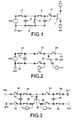
Le schéma de principe d'un interrupteur 1
commandé par un signal en « clock-doubling » est
représenté sur la figure 1.The schematic diagram of a
Un tel dispositif met en oeuvre des
capacités 2, 4.Such a device implements
Au cours d'une première phase, ces deux
capacités sont chargées à Vdd par fermeture des
interrupteurs 6, 8, 12.During a first phase, these two
Capacities are loaded at Vdd by
Au cours d'une deuxième phase, l'armature
inférieure de l'une est connectée à l'armature
supérieure de l'autre, par fermeture de l'interrupteur
10, formant ainsi une capacité série chargée à une
tension 2Vdd.During a second phase, the reinforcement
bottom of one is connected to the armature
superior of the other, by closing the
On peut ainsi commander le transistor 1 via
l'interrupteur 14, avec une tension 2Vdd.It is thus possible to control
Bien qu'efficace, cette technique est
stressante pour le transistor 1. Elle engendre en effet
des tensions Grille - Source de valeur 2Vdd et peut
donc détériorer l'oxyde de grille du transistor 1.Although effective, this technique is
stressful for the
On lui préfère donc la technique dite de « Clock Boosting », décrite par M. Dessouky et A. Kaiser dans « Input switch configuration for suitable rail-to-rail operation of switched opamps circuits », IEE Electronic Letters, 35(1), 1999, pour laquelle la tension grille-source est fixée à Vdd quelle que soit la tension du signal.So we prefer him the so-called technique of "Clock Boosting", described by Mr. Dessouky and A. Kaiser in "Input switch configuration for suitable rail-to-rail operation of switched opamps circuits ", IEE Electronic Letters, 35 (1), 1999, for which gate-source voltage is set to Vdd whatever the signal voltage.
Le principe du « clock Boosting » est représenté sur la figure 2.The principle of "clock boosting" is shown in Figure 2.
Une capacité 20 est chargée pendant une
première phase (par fermeture des interrupteurs 24 et
26) et est appliquée aux bornes grille/source d'un
transistor 22 pendant une deuxième phase (par fermeture
des interrupteurs 32 et 34), durant laquelle elle agit
comme une batterie. Pendant la première phase, le
transistor 28 est fermé : la grille du transistor 22
est à la masse ou au potentiel GND.A
Cette technique permet une amélioration sensible des performances d'un interrupteur d'entrée : la distorsion harmonique, entre autre, est réduite d'un facteur dix à cent par rapport aux solutions classiques à base d'interrupteurs de polarités complémentaires (CMOS).This technique allows an improvement sensitive performance of an input switch: harmonic distortion, among others, is reduced by one factor ten to one hundred compared to conventional solutions based on switches of complementary polarities (CMOS).
Les performances de ces interrupteurs ne sont pourtant pas assez satisfaisantes en regard de la linéarité souhaitée, notamment pour des applications de télécommunication réalisées en capacités commutées.The performance of these switches are not satisfactory enough with regard to the desired linearity, in particular for telecommunications carried out in switched capacities.
Il se pose donc le problème de réaliser un procédé et un dispositif de commande d'un interrupteur analogique à distorsion harmonique réduite.There is therefore the problem of achieving a method and a device for controlling a switch harmonic distortion analog.
L'invention proposée permet de réduire la distorsion harmonique introduite par un interrupteur analogique, utilisant notamment un transistor, par exemple de type MOS.The proposed invention reduces the harmonic distortion introduced by a switch analogue, including a transistor, for example example of MOS type.
L'invention a pour objet un procédé de commande d'un interrupteur analogique comportant un transistor auquel est appliquée une tension d'entrée Vin, procédé dans lequel :
- on applique à la grille du transistor, pendant une première phase, une première tension, dépendante ou fonction de la tension d'entrée Vin et d'un premier potentiel V1, la première tension étant apte à rendre ledit transistor passant,
- on applique à la grille du transistor, pendant une deuxième phase, une deuxième tension, dépendante ou fonction de la tension d'entrée Vin et d'un deuxième potentiel V2, la deuxième tension étant apte à bloquer ledit transistor, la différence entre la première tension et la deuxième tension étant indépendante de la tension d'entrée Vin.
- a first voltage, dependent or a function of the input voltage Vin and a first potential V1, is applied to the gate of the transistor during a first phase, the first voltage being able to make said transistor passing,
- a second voltage dependent on or a function of the input voltage Vin and a second potential V2 is applied to the gate of the transistor during a second phase, the second voltage being able to block said transistor, the difference between the first voltage voltage and the second voltage being independent of the input voltage Vin.
Selon une première variante du procédé pour laquelle le transistor est un transistor de type N, la première tension peut être égale à Vin + V1, tandis que la deuxième tension peut être égale à Vin + V2.According to a first variant of the method for which the transistor is an N-type transistor, the first voltage can be equal to Vin + V1, while the second voltage can be equal to Vin + V2.
Selon une deuxième variante du procédé pour laquelle le transistor est un transistor de type P, la première tension peut être égale à Vin - V1, tandis que la deuxième tension peut être égale à Vin - V2.According to a second variant of the method for which transistor is a P-type transistor, the first voltage can be equal to Vin - V1, while the second voltage may be equal to Vin - V2.
Le premier potentiel et le deuxième potentiel peuvent être des potentiels fixes ou constants.The first potential and the second potential can be fixed potentials or constant.
Le premier potentiel V1 peut être supérieur à la tension de seuil dudit transistor. Le premier potentiel V1 peut être également positif.The first potential V1 can be higher at the threshold voltage of said transistor. The first potential V1 can be also positive.
Le deuxième potentiel V2 peut être inférieur à la tension de seuil dudit transistor.The second potential V2 can be less than the threshold voltage of said transistor.
Selon une possibilité de mise en oeuvre, le premier potentiel V1 et le deuxième potentiel V2 peuvent être égaux en valeur absolue ou être tels que V1=-V2.According to one possibility of implementation, the first potential V1 and second potential V2 may be equal in absolute value or be such that V1 = -V2.
Selon une variante, le premier potentiel et le deuxième potentiel peuvent être égaux en valeur absolue à une tension Vdd ou être tels que V1=-V2=Vdd. Une telle variante peut permettre de maximiser la conductance du transistor à l'état passant et de minimiser les fuites du transistor à l'état bloqué. La tension Vdd peut être une tension supérieure à la tension de seuil du transistor. La tension Vdd peut être une tension de polarisation ou une tension maximale autorisée par la filière technologique du transistor.According to one variant, the first potential and the second potential can be equal in value absolute at a voltage Vdd or be such that V1 = -V2 = Vdd. Such a variant can make it possible to maximize the conductance of the transistor in the on state and minimize leakage of the transistor in the off state. The voltage Vdd can be a voltage greater than the threshold voltage of the transistor. The voltage Vdd can to be a bias voltage or a voltage authorized by the technological sector of the transistor.
L'invention a également pour objet un procédé de commande d'un interrupteur analogique comportant un transistor, auquel est appliquée une tension d'entrée Vin, procédé dans lequel on applique au transistor un signal d'horloge, ou un signal de grille ou de commande, symétrique par rapport à la tension d'entrée.The invention also relates to a method of controlling an analog switch having a transistor, to which a Vin input voltage, in which method is applied to the transistor a clock signal, or a signal of grid or control, symmetrical with respect to the input voltage.
L'invention met également en oeuvre un procédé de commande d'un interrupteur analogique comportant un transistor, auquel est appliquée une tension d'entrée Vin, procédé dans lequel :
- on applique à la grille du transistor, pendant une première phase, une première tension, Vin + Vdd,
- on applique à la grille du transistor, pendant une deuxième phase, une deuxième tension, Vin - Vdd, symétrique de la première tension par rapport à la tension d'entrée Vin.
- a first voltage, Vin + Vdd, is applied to the gate of the transistor during a first phase,
- a second voltage, Vin-Vdd, symmetrical with the first voltage with respect to the input voltage Vin, is applied to the gate of the transistor during a second phase.
Selon l'invention, pour réduire la distorsion harmonique due à l'erreur d'injection de charge, on rend cette erreur la plus indépendante possible du signal. According to the invention, to reduce the harmonic distortion due to the injection error of load, we make this error the most independent possible signal.
La première tension Vin + Vdd peut être appliquée, pendant la première phase, par application d'un premier condensateur chargé à Vdd, entre la grille et une tension d'entrée Vin ou un noeud au potentiel Vin.The first voltage Vin + Vdd can be applied, during the first phase, by application a first capacitor charged to Vdd, between the gate and a Vin input voltage or a potential node Wine.
La deuxième tension Vin - Vdd peut être appliquée, pendant la deuxième phase, par application d'un deuxième condensateur chargé à - Vdd, entre la grille et la tension d'entrée Vin, ou un noeud au potentiel Vin, ou la tension de sortie VST.The second voltage Vin-Vdd can be applied, during the second phase, by applying a second capacitor charged at -Vdd, between the gate and the input voltage Vin, or a node at the potential Vin, or the output voltage V ST .
Le deuxième condensateur peut se recharger pendant la première phase, le premier condensateur se rechargeant pendant la deuxième phase.The second capacitor can recharge during the first phase, the first capacitor recharging during the second phase.
La première tension peut être appliquée par commutation d'au moins un interrupteur.The first voltage can be applied by switching of at least one switch.
La deuxième tension peut être appliquée par commutation d'au moins un interrupteur.The second voltage can be applied by switching of at least one switch.
Le premier condensateur peut être chargé à partir d'une source de tension Vdd dont il est isolé, en cours de décharge, par un transistor dont la grille est reliée à la grille du transistor de l'interrupteur analogique.The first capacitor can be charged to from a voltage source Vdd from which it is isolated, being discharged, by a transistor whose gate is connected to the transistor gate of the switch analog.
Ce transistor peut être à l'état bloqué lorsque la grille du transistor de l'interrupteur analogique est à l'état haut et étant à l'état passant lorsque la grille du transistor de l'interrupteur analogique est à l'état bas.This transistor can be in the off state when the transistor gate of the switch analog is in the high state and in the on state when the transistor gate of the switch analog is in the low state.
La deuxième tension est de préférence appliquée via un transistor à corps flottant ou à n (n>2) caissons. The second tension is preferably applied via a floating-body or n-type transistor (n> 2) caissons.
Le deuxième condensateur peut être relié à la masse dont il est isolé, en cours de décharge, par un transistor dont la grille est reliée à la grille du transistor de l'interrupteur analogique.The second capacitor can be connected to the mass from which it is isolated, being discharged, by a transistor whose gate is connected to the gate of the transistor of the analog switch.
Le transistor peut être à l'état bloqué lorsque la grille du transistor de l'interrupteur analogique est à l'état bas et étant à l'état passant lorsque la grille du transistor de l'interrupteur analogique est à l'état haut.The transistor can be in the off state when the transistor gate of the switch analogue is in the low state and in the on state when the transistor gate of the switch analog is in the high state.
L'invention concerne également un dispositif de commande d'un interrupteur analogique comportant un transistor, ce dispositif de commande comportant :
- des moyens pour appliquer une tension d'entrée Vin audit transistor,
- des moyens pour appliquer à la grille du transistor, pendant une première phase, une première tension dépendante ou fonction de la tension d'entrée Vin et d'un premier potentiel V1, la première tension étant apte à rendre passant ledit transistor,
- des moyens pour appliquer à la grille du transistor, pendant une deuxième phase, une deuxième tension, dépendante ou fonction de la tension d'entrée Vin et d'un deuxième potentiel V2, la deuxième tension étant apte à rendre bloqué ledit transistor, la différence entre la première tension et la deuxième tension étant indépendante de vin.
- means for applying an input voltage Vin to said transistor,
- means for applying to the gate of the transistor, during a first phase, a first voltage dependent or a function of the input voltage Vin and a first potential V1, the first voltage being able to turn on said transistor,
- means for applying to the gate of the transistor, during a second phase, a second voltage, dependent or a function of the input voltage Vin and a second potential V2, the second voltage being able to block said transistor, the difference between the first voltage and the second voltage being independent of wine.
Selon une première variante pour laquelle le transistor est un transistor de type N, la première tension peut être égale à Vin + V1, tandis que la deuxième tension peut être égale à Vin + V2. According to a first variant for which the transistor is an N-type transistor, the first voltage can be equal to Vin + V1, while the second voltage can be equal to Vin + V2.
Selon une seconde variante pour laquelle le transistor est un transistor de type P, la première tension peut être égale à Vin - V1, tandis que la deuxième tension peut être égale à Vin - V2.According to a second variant for which the transistor is a P-type transistor, the first voltage can be equal to Vin - V1, while the second voltage can be equal to Vin - V2.
Le premier potentiel V1 et le deuxième potentiel V2 peuvent être des potentiels fixes ou constants.The first potential V1 and the second potential V2 can be fixed potentials or constant.
Le premier potentiel V1 peut être positif et supérieur à la tension de seuil dudit transistor.The first potential V1 can be positive and greater than the threshold voltage of said transistor.
Le deuxième potentiel V2 peut être inférieur à la tension de seuil dudit transistor.The second potential V2 can be less than the threshold voltage of said transistor.
Selon une possibilité de mise en oeuvre, le premier potentiel V1 et le deuxième potentiel V2 peuvent être tels que V1=-V2.According to one possibility of implementation, the first potential V1 and second potential V2 can be such that V1 = -V2.
Selon une variante, le premier potentiel V1 et le deuxième potentiel V2 peuvent être tels que V1=-V2=Vdd.According to one variant, the first potential V1 and the second potential V2 can be such that V1 = -V2 = Vdd.
La tension Vdd peut être supérieure à la tension de seuil du transistor. La tension Vdd peut être une tension de polarisation ou une tension maximale autorisée par la filière technologique du transistor.The voltage Vdd may be greater than the threshold voltage of the transistor. The voltage Vdd can to be a bias voltage or a voltage authorized by the technological sector of the transistor.
L'invention concerne également un dispositif de commande d'un interrupteur analogique comportant un transistor, ce dispositif de commande comportant :
- des moyens pour appliquer une tension d'entrée Vin,
- des moyens pour appliquer à la grille du transistor, pendant une première phase, une première tension, Vin + Vdd,
- des moyens pour appliquer à la grille du transistor, pendant une deuxième phase, une deuxième tension, Vin - Vdd, symétrique de la première par rapport à la tension d'entrée Vin.
- means for applying an input voltage Vin,
- means for applying to the gate of the transistor, during a first phase, a first voltage, Vin + Vdd,
- means for applying to the gate of the transistor, during a second phase, a second voltage, Vin-Vdd, symmetrical to the first with respect to the input voltage Vin.
Un premier condensateur peut permettre d'appliquer la première tension Vin + Vdd, pendant la première phase, entre la grille et la tension d'entrée Vin.A first capacitor can allow to apply the first voltage Vin + Vdd, during the first phase, between the gate and the input voltage Wine.
Un deuxième condensateur peut permettre d'appliquer la deuxième tension Vin - Vdd, pendant la deuxième phase, entre la grille et la tension d'entrée Vin, ou la tension de sortie VST.A second capacitor can make it possible to apply the second voltage Vin-Vdd, during the second phase, between the gate and the input voltage Vin, or the output voltage V ST .
Des moyens peuvent permettre de recharger le deuxième condensateur pendant la première phase et d'autres moyens peuvent permettre de recharger le premier condensateur pendant la deuxième phase.Means can reload the second capacitor during the first phase and other means can be used to recharge the first capacitor during the second phase.
Avantageusement, le dispositif comporte au moins un interrupteur pour appliquer la première tension.Advantageously, the device comprises at least a switch to apply the first voltage.
Il peut en outre comporter au moins un interrupteur pour appliquer la deuxième tension.It may also include at least one switch to apply the second voltage.
Selon un mode de réalisation, il comporte une source de tensions Vdd pour charger le premier condensateur et des moyens pour isoler, en cours de décharge, la source de tension du premier condensateur.According to one embodiment, it comprises a source of voltages Vdd to charge the first capacitor and means for isolating, in the course of discharge, the voltage source of the first capacitor.
Des moyens peuvent être prévus pour isoler, en cours de décharge, la source de tension du premier condensateur.Means can be provided to isolate, being discharged, the voltage source of the first capacitor.
Ces moyens comportent par exemple un transistor dont la grille est reliée à la grille du transistor de l'interrupteur analogique. These means comprise for example a transistor whose gate is connected to the gate of the transistor of the analog switch.
Ledit transistor peut être à l'état bloqué lorsque la grille du transistor de l'interrupteur analogique est à l'état haut et à l'état passant lorsque la grille du transistor de l'interrupteur analogique est à l'état bas.Said transistor can be in the off state when the transistor gate of the switch analogue is in the high state and in the on state when the transistor gate of the switch analog is in the low state.
Avantageusement, un transistor à corps flottant ou à n (n>2) caissons permet d'appliquer la deuxième tension.Advantageously, a transistor with a body floating or n (n> 2) boxes allows to apply the second voltage.
Le deuxième condensateur peut être relié à la masse dont il est isolé, en cours de décharge, par un transistor dont la grille est reliée à la grille du transistor de l'interrupteur analogique.The second capacitor can be connected to the mass from which it is isolated, being discharged, by a transistor whose gate is connected to the gate of the transistor of the analog switch.
Ledit transistor peut être à l'état bloqué lorsque la grille du transistor de l'interrupteur analogique est à l'état bas et à l'état passant lorsque la grille du transistor de l'interrupteur analogique est à l'état haut.Said transistor can be in the off state when the transistor gate of the switch analogue is in the low state and in the on state when the transistor gate of the analog switch is in the high state.
Un exemple de circuit selon l'invention est illustré en figure 3.An example circuit according to the invention is illustrated in Figure 3.
Ce circuit permet d'améliorer la linéarité des interrupteurs, malgré l'erreur d'injection de charge, grâce à un nouveau principe d'horloge, plus symétrique par rapport au signal.This circuit improves linearity switches, despite the injection error of charge, thanks to a new clock principle, more symmetrical with respect to the signal.
Selon l'invention, on applique sur la
grille d'un transistor 50, en particulier de type MOS :
pendant une première phase, une première tension,
dépendante ou fonction d'une tension d'entrée Vin et
d'un premier potentiel V1, la première tension étant
apte à rendre ledit transistor passant. Puis, on
applique à la grille du transistor, pendant une
deuxième phase, une deuxième tension, dépendante ou
fonction de la tension d'entrée Vin et d'un deuxième
potentiel V2, la deuxième tension étant apte à bloquer
ledit transistor, la différence entre la première
tension et la deuxième tension étant indépendante de la
tension d'entrée Vin. L'injection de charge au niveau
du transistor peut être ainsi rendue d'avantage
indépendante du signal d'entrée.According to the invention,
gate of a
Le transistor 50 peut être par exemple un
transistor de type N. La première tension peut être
égale à vin + V1, tandis que la deuxième tension peut
être égale à vin + V2. The
Le premier potentiel V1 et le deuxième potentiel V2 peuvent être des potentiels fixes ou constants. Le premier potentiel V1 peut être supérieur à la tension de seuil dudit transistor. Le premier potentiel V1 peut être également positif. Le deuxième potentiel V2 peut être inférieur à la tension de seuil dudit transistor. Selon une possibilité de mise en oeuvre, le premier potentiel V1 et le deuxième potentiel V2 peuvent être égaux en valeur absolue ou être tels que V1=-V2. Selon une variante, le premier potentiel et le deuxième potentiels peuvent être égaux en valeur absolue à une tension Vdd ou être tels que V1=-V2=Vdd, avec Vdd une tension de polarisation, supérieure à la tension de seuil du transistor.The first potential V1 and the second potential V2 can be fixed potentials or constant. The first potential V1 can be higher at the threshold voltage of said transistor. The first potential V1 can be also positive. The second potential V2 may be lower than the threshold voltage said transistor. According to a possibility of implementation the first potential V1 and the second potential V2 may be equal in absolute value or be such that V1 = -V2. According to one variant, the first potential and the second potential can be equal in value absolute at a voltage Vdd or be such that V1 = -V2 = Vdd, with Vdd a bias voltage higher than the threshold voltage of the transistor.
Selon cette variante, on applique sur la
grille d'un transistor 50, par exemple de type NMOS,
des tensions symétriques, par rapport à une tension Vin
d'entrée d'un transistor interrupteur, pendant une
première phase puis pendant une deuxième phase.According to this variant, it is applied on the
gate of a
La tension Vin d'entrée provient par exemple d'un microphone, d'une ligne téléphonique de type ADSL ou encore d'une chaíne de réception radiofréquence.The Vin input voltage comes through example of a microphone, a telephone line type ADSL or a radio frequency reception channel.
Une tension égale à Vin + Vdd est appliquée durant une première phase, ou état « on », et une tension égale à Vin - Vdd est appliquée durant une deuxième phase, ou état « off ».A voltage equal to Vin + Vdd is applied during a first phase, or "on" state, and a voltage equal to Vin - Vdd is applied during a second phase, or "off" state.
Ceci permet de rendre l'erreur d'injection de charge quasiment indépendante de la valeur du signal, réduisant ainsi la distorsion harmonique. This makes the injection error charge almost independent of the value of the signal, thereby reducing harmonic distortion.
Pendant la première phase, un condensateur
42 initialement chargé à Vdd, (par fermeture des
interrupteurs 46 et 62) est appliqué entre la grille 51
du transistor 50 et Vin (par fermeture des
interrupteurs 48 et 60).During the first phase, a
Une tension égale à Vdd + Vin est alors
appliquée à cette grille 51.A voltage equal to Vdd + Vin is then
applied to this
Pendant la même phase, un deuxième
condensateur 44 se recharge à la tension -Vdd (par
fermeture des interrupteurs 54 et 56).During the same phase, a
Pendant une deuxième phase, le premier
condensateur se recharge (les interrupteurs 48 et 60
sont ouverts et les interrupteurs 46 et 62 fermés)
tandis que le condensateur 44 est appliqué entre la
grille et le drain du transistor 50, mais avec une
tension de signe opposé au premier. En variante, le
condensateur pourrait être appliqué entre la grille et
la source du transistor 50. En effet, en fin de charge,
source et drain sont au même potentiel (Vin=VST).During a second phase, the first capacitor recharges (the
Ceci a pour effet d'appliquer une tension
Vin-Vdd sur la grille du transistor 51.This has the effect of applying a voltage
Vin-Vdd on the gate of
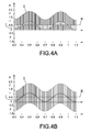
Les figures 4A et 4B montrent plusieurs cycles de charge et de décharge d'une capacité par un interrupteur analogique par un signal sinusoïdal, le graphique du bas (figure 4B) correspondant à un cas symétrique, selon l'invention, celui du haut (figure 4A) au cas de « clock-boosting » connu.Figures 4A and 4B show several cycles of charging and discharging a capacitance by a analog switch by a sinusoidal signal, the bottom graph (Figure 4B) corresponding to a case symmetrical, according to the invention, that of the top (FIG. 4A) in the known "clock-boosting" case.
Sur chaque graphe sont représentés les signaux d'entrée (courbe I), de sortie (entre la courbe I et la ligne horizontale III) et de commande (ou de grille : courbe II). On each graph are represented the input signals (curve I), output (between the curve I and the horizontal line III) and command (or grid: curve II).
On voit, sur le graphique du bas, que le signal de grille tout à fait symétrique par rapport au signal d'entrée I et au signal de sortie, qui peuvent avoir une fréquence pouvant aller jusqu'à quelques centaines de MégaHertz.We can see on the bottom graph that the grid signal quite symmetrical with respect to the input signal I and the output signal, which can have a frequency up to a few hundreds of MegaHertz.
La figure 5 illustre une réalisation détaillée d'un circuit selon l'invention.Figure 5 illustrates an embodiment of a circuit according to the invention.
Ce circuit permet de générer des horloges pouvant atteindre +2Vdd et -Vdd à partir d'une alimentation de Vdd.This circuit makes it possible to generate clocks up to + 2Vdd and -Vdd from a Vdd power supply.
L'explication du fonctionnement de ce circuit est la suivante.The explanation of how this circuit is as follows.
Pendant une première phase, ou phase
« on », une capacité 70, initialement chargée à Vdd,
est appliqué entre l'entrée 72 et la grille 74 via des
transistors 76, et 78, 80 qui forment un interrupteur
en structures MOS à polarités complémentaires.During a first phase, or phase
"On", a
L'armature négative de la capacité 70 est
connectée à l'entrée 72 (à la tension Vin) et son
armature positive à la grille 74. Le signal grille
monte donc à une tension V = Vin + Vdd.The negative armature of the
A ce moment, le transistor 82 qui, avec le
transistor 83, permet de charger la capacité 90 à Vdd,
pourrait se mettre à conduire puisque sa source monte à
une tension supérieure à sa grille.At this moment, the
Le résultat serait que le signal de grille se déchargerait dans la source de tension Vdd.The result would be that the grid signal would discharge into the voltage source Vdd.
Pour empêcher ceci, un transistor 84 est
mis en série sur ce noeud.To prevent this, a
Ce transistor, dont la grille est connectée
à la grille 74, permet d'isoler la source de tension à
Vdd de la grille 74, quand cette dernière est à l'état
haut. Il est passant quand la grille 74 est à l'état
bas.This transistor, whose gate is connected
at the
Toujours pendant la première phase, les
transistors 86 et 88 chargent la capacité 90 à une
tension Vdd.During the first phase,
Tous les autres transistors sont à l'état haute impédance.All other transistors are in the state high impedance.
A la fin de cette première phase, les
transistors 76, et 78, 80 sont coupés et isolent ainsi
la capacité de la grille 74.At the end of this first phase,
Au début de la deuxième phase, ou état
« off », les transistors 92, 94 deviennent passant et
connectent l'armature positive de la capacité 90 au
signal Vin.At the beginning of the second phase, or state
"Off", the
Il est aussi possible de connecter cette armature au signal Vst puisque, en fin de charge (fin de l'état « on ») les tensions Vin et Vst sont les mêmes.It is also possible to connect this armature to the signal Vst since, at the end of charge (end of the "on" state) the voltages Vin and Vst are the same.
Lorsque la tension de grille (74) plonge
sous le niveau 0, le transistor 86 peut se retrouver
avec une tension grille-source positive, se mettre à
conduire et ainsi décharger la capacité 90 dans la
masse.When the gate voltage (74) dives
under
Pour empêcher ceci, on a recours à un
transistor 87 en série sur le chemin masse 89-grille 74
et dont la grille est reliée à la grille 74. Ce
transistor est bloqué et isole la masse 89 de la grille
74 lorsque cette dernière est à l'état bas et est
transparent lorsqu'elle est à l'état haut. To prevent this, we use a
Toujours pendant l'état « off », les
transistors 82 et 83 sont passants pour recharger les
pertes de charges de la capacité 70. A la fin de la
phase « off », les transistors 96 et 92,94 sont coupés,
isolant ainsi la capacité 90 de la grille 74.Always during the "off" state, the
L'armature négative de la capacité 90 est
connectée à la grille 74 par le transistor 96. Le
signal de grille 74 descend donc à la tension V' = Vin
- Vdd (ou Vst - Vdd).The negative armature of the
Cette tension peut être voisine de -Vdd
dans le cas où Vin est proche de 0 ; dans ce cas, la
diode source/substrat du transistor 96 peut se
retrouver en direct ce qui empêche le noeud 74 de
descendre en dessous de -Vdiode.This voltage can be close to -Vdd in the case where Vin is close to 0; in this case, the source / substrate diode of the
Les technologies SOI permettent de résoudre
ce problème en raison de l'isolation complète du corps
et rendent donc possible cette génération de tensions
de commandes négatives. On utilise en particulier un
transistor 96 à corps flottant.SOI technologies solve
this problem because of the complete isolation of the body
and thus make possible this generation of tensions
negative orders. In particular, a
D'autres technologies telles que les technologies à triple caisson peuvent également être utilisées.Other technologies such as triple-box technologies can also be used.
Les figures 7 et 8 illustrent le principe d'isolation source/substrat, respectivement pour les technologies SOI et triple caisson.Figures 7 and 8 illustrate the principle source / substrate isolation, respectively for SOI and triple box technologies.
Sur les figures 6 - 8, trois transistors MOS de type N sont représentés en coupe pour les technologies standard (figure 6), SOI (figure 7) et triple caisson (figure 8). In Figures 6 - 8, three transistors MOS type N are shown in section for standard technologies (Figure 6), SOI (Figure 7) and triple box (Figure 8).
Dans la technologie standard (figure 6)
deux diodes substrat/drain 130 et substrat/source 132
apparaissent.In standard technology (Figure 6)
two substrate /
Le substrat 131 étant connecté à la masse,
toute tension inférieure à la masse moins un seuil de
diode rend l'une de ces diodes passante.The
Ce problème est résolu en technologie SOI
(figure 7) où un isolant 134 sépare le substrat 141 du
drain 140 et de la source 142.This problem is solved in SOI technology
(FIG. 7) where an
Les technologies à triple caissons (figure 8) compensent également le problème par un caisson externe 153 dopé N- (dans un substrat 151 P-).Triple-box technologies (figure 8) also compensate the problem by a box external N-doped 153 (in a 151 P- substrate).
Ce caisson externe contient un autre caisson dopé 155 P- permettant la constitution d'un transistor MOS de type N.This external box contains another 155 P-doped caisson allowing the constitution of a N-type MOS transistor.
Cette construction permet d'obtenir une diode inverse caisson/substrat qui empêche l'épanchement d'une tension négative dans la masse du substrat.This construction makes it possible to obtain reverse diode box / substrate that prevents the effusion of a negative voltage in the mass of the substrate.
Les figures 9A - 9C résument les différents principes de tension de grille du transistor interrupteur : de gauche à droite sont représentées le principe d'une tension de grille standard (figure 9A), le principe d'une tension de grille avec un « clock-boosting » (figure 9B) et enfin le principe d'une tension de grille avec « clock-boosting » symétrique (figure 9C). La tension Vin est représentée en pointillées. Le signal ou la tension de grille ou de commande constitue le signal d'horloge.Figures 9A-9C summarize the different gate voltage principles of the transistor switch: from left to right are represented on principle of a standard gate voltage (FIG. 9A), the principle of a gate voltage with a clock-boosting (Figure 9B) and finally the principle of gate voltage with symmetrical clock-boosting (Figure 9C). The voltage Vin is represented in dashed. The signal or the gate or gate voltage command constitutes the clock signal.
La figure 10 montre des résultats d'une simulation respectivement pour un procédé selon l'invention, en « clock-boosting » symétrique (courbe I) et celle de « clock-boosting » non symétrique (courbe II).Figure 10 shows results of a simulation respectively for a process according to the invention, in symmetrical clock-boosting (curve I) and that of non-symmetrical clock-boosting (curve II).
La distorsion harmonique d'un transistor N monté en interrupteur d'entrée y est tracée en fonction de sa largeur W.The harmonic distortion of a transistor N mounted as an input switch is traced according to W. Width
Les résultats montrent un gain de la technique symétrique par rapport à la non symétrique, quelle que soit la largeur du transistor.The results show a gain in symmetrical technique compared to the non-symmetrical, whatever the width of the transistor.
Le minimum de distorsion est lui aussi amélioré, d'environ 10dB.The minimum of distortion is also improved, about 10dB.
L'invention permet l'amélioration de la linéarité des interrupteurs analogiques et permet donc l'amélioration des performances de ces composants utilisés dans de nombreux domaines dont, en particulier, les applications de télécommunication, les convertisseurs analogiques numériques et les circuits à capacités commutées.The invention allows the improvement of the linearity of analog switches and thus allows improving the performance of these components used in many areas including, in particular, telecommunication applications, analog digital converters and circuits to switched capabilities.
Elle représente une nouvelle solution à l'erreur d'injection de charges qui va devenir de plus en plus prépondérante avec la diminution de l'oxyde de grille et des tensions d'alimentation.It represents a new solution to the charge injection error that will become more in addition to preponderant with the decrease of the oxide of grid and supply voltages.
Elle s'applique particulièrement bien aux
technologies isolées de type SOI qui permettent de
réaliser des transistors à corps flottant, comme
expliqué ci-dessus, en particulier pour le transistor
96.It applies particularly well to
isolated SOI technologies that allow
make floating-body transistors, as
explained above, especially for the
L'invention n'est pas limitée à une commande de transistors de type N et peut s'appliquer à des transistors de type P, en particulier à des transistors de type PMOS. Dans ce cas, on peut appliquer sur la grille d'un transistor PMOS, pendant une première phase, une première tension Vin - V1, la première tension étant apte à rendre ledit transistor passant, puis, pendant une deuxième phase, une deuxième tension Vin - V2, la deuxième tension étant apte à bloquer ledit transistor, la différence entre la première tension et la deuxième tension étant indépendante de la tension d'entrée Vin.The invention is not limited to control of N-type transistors and can apply to P-type transistors, in particular to PMOS type transistors. In this case, we can apply to the gate of a PMOS transistor, while a first phase, a first voltage Vin - V1, the first voltage being adapted to render said transistor passing, then, during a second phase, a second voltage Vin - V2, the second voltage being suitable for block said transistor, the difference between first voltage and the second voltage being independent of the input voltage Vin.
Claims (33)
Applications Claiming Priority (2)
| Application Number | Priority Date | Filing Date | Title |
|---|---|---|---|
| FR0451266A FR2871630B1 (en) | 2004-06-11 | 2004-06-11 | METHOD FOR CONTROLLING AN ANALOG SWITCH |
| FR0451266 | 2004-06-11 |
Publications (3)
| Publication Number | Publication Date |
|---|---|
| EP1608069A2 true EP1608069A2 (en) | 2005-12-21 |
| EP1608069A3 EP1608069A3 (en) | 2006-04-26 |
| EP1608069B1 EP1608069B1 (en) | 2007-08-08 |
Family
ID=34940145
Family Applications (1)
| Application Number | Title | Priority Date | Filing Date |
|---|---|---|---|
| EP05105121A Not-in-force EP1608069B1 (en) | 2004-06-11 | 2005-06-10 | Method for controling an analog switch |
Country Status (5)
| Country | Link |
|---|---|
| US (1) | US7274222B2 (en) |
| EP (1) | EP1608069B1 (en) |
| AT (1) | ATE369658T1 (en) |
| DE (1) | DE602005001896T2 (en) |
| FR (1) | FR2871630B1 (en) |
Cited By (1)
| Publication number | Priority date | Publication date | Assignee | Title |
|---|---|---|---|---|
| ES2478791A1 (en) * | 2013-01-22 | 2014-07-22 | Universitat De Les Illes Balears | Switch with modifiable resistance (Machine-translation by Google Translate, not legally binding) |
Families Citing this family (12)
| Publication number | Priority date | Publication date | Assignee | Title |
|---|---|---|---|---|
| EP2080273B1 (en) * | 2006-11-10 | 2018-09-05 | Skyworks Solutions, Inc. | Compact low loss high frequency switch with improved linearity performance |
| US7710164B1 (en) * | 2007-06-18 | 2010-05-04 | Intersil Americas Inc. | Highly linear bootstrapped switch with improved reliability |
| US20090039924A1 (en) * | 2007-08-09 | 2009-02-12 | Alfio Zanchi | Systems and methods for reducing distortion in semiconductor based sampling systems |
| US8030974B1 (en) | 2008-09-10 | 2011-10-04 | Marvell International, Ltd. | Method and apparatus for sampling |
| US8183890B1 (en) * | 2008-09-10 | 2012-05-22 | Marvell International Ltd. | Method and apparatus for sampling |
| US7940091B1 (en) * | 2009-03-02 | 2011-05-10 | Linear Technology Corporation | Bootstrapped switch for sampling voltages beyond the supply voltage |
| US8289066B2 (en) * | 2009-12-30 | 2012-10-16 | Stmicroelectronics Asia Pacific Pte Ltd. | Gate control circuit for high bandwidth switch design |
| FR2968808A1 (en) * | 2010-12-08 | 2012-06-15 | Commissariat Energie Atomique | ELECTRONIC CIRCUIT WITH NEUROMORPHIC ARCHITECTURE |
| US8593181B2 (en) * | 2011-08-04 | 2013-11-26 | Analog Devices, Inc. | Input switches in sampling circuits |
| US8525574B1 (en) * | 2012-05-15 | 2013-09-03 | Lsi Corporation | Bootstrap switch circuit with over-voltage prevention |
| EP3429080A1 (en) * | 2017-07-14 | 2019-01-16 | Fraunhofer-Gesellschaft zur Förderung der angewandten Forschung e.V. | Switch device for switching an analog electrical input signal |
| TWI774564B (en) * | 2021-09-23 | 2022-08-11 | 瑞昱半導體股份有限公司 | Bootstrapped switch |
Citations (4)
| Publication number | Priority date | Publication date | Assignee | Title |
|---|---|---|---|---|
| EP0899714A2 (en) * | 1997-08-29 | 1999-03-03 | Sony Corporation | Column driver for an active matrix liquid crystal display |
| WO1999013592A1 (en) * | 1997-09-09 | 1999-03-18 | Watkins-Johnson Company | Totem pole mixer having grounded serially connected stacked fet pair |
| EP1168619A1 (en) * | 2000-06-19 | 2002-01-02 | STMicroelectronics S.r.l. | Boosted switch device for a sampler of an analogue/digital converter, and operating method thereof |
| US6522187B1 (en) * | 2001-03-12 | 2003-02-18 | Linear Technology Corporation | CMOS switch with linearized gate capacitance |
Family Cites Families (12)
| Publication number | Priority date | Publication date | Assignee | Title |
|---|---|---|---|---|
| US6072353A (en) * | 1995-04-26 | 2000-06-06 | Matsushita Electric Industrial Co., Ltd. | Logic circuit with overdriven off-state switching |
| US6052000A (en) * | 1997-04-30 | 2000-04-18 | Texas Instruments Incorporated | MOS sample and hold circuit |
| US5945872A (en) * | 1997-11-06 | 1999-08-31 | Analog Devices, Inc. | Two-phase boosted CMOS switch drive technique and circuit |
| FR2793970B1 (en) * | 1999-05-20 | 2001-08-31 | St Microelectronics Sa | METHOD FOR CONTROLLING A SWITCH OF A SWITCHED CAPACITY DEVICE, AND CORRESPONDING SWITCHED CAPACITY DEVICE |
| US6310565B1 (en) * | 2000-02-03 | 2001-10-30 | Lucent Technologies Inc. | Sampling switch having an independent “on” impedance |
| US6323697B1 (en) * | 2000-06-06 | 2001-11-27 | Texas Instruments Incorporated | Low distortion sample and hold circuit |
| US6833753B2 (en) * | 2002-11-27 | 2004-12-21 | Texas Instruments Incorporated | Method and system for signal dependent boosting in sampling circuits |
| US7053692B2 (en) * | 2002-12-19 | 2006-05-30 | United Memories, Inc. | Powergate control using boosted and negative voltages |
| US6956411B1 (en) * | 2003-03-27 | 2005-10-18 | National Semiconductor Corporation | Constant RON switch circuit with low distortion and reduction of pedestal errors |
| DE60308346D1 (en) * | 2003-07-03 | 2006-10-26 | St Microelectronics Srl | With voltage increase operated sampling circuit and associated control method |
| KR20060054418A (en) * | 2003-08-04 | 2006-05-22 | 코닌클리즈케 필립스 일렉트로닉스 엔.브이. | Track-and-hold circuit |
| JP4128545B2 (en) * | 2004-05-20 | 2008-07-30 | 富士通株式会社 | Sampling switch |
-
2004
- 2004-06-11 FR FR0451266A patent/FR2871630B1/en not_active Expired - Fee Related
-
2005
- 2005-06-10 US US11/149,216 patent/US7274222B2/en not_active Expired - Fee Related
- 2005-06-10 DE DE602005001896T patent/DE602005001896T2/en active Active
- 2005-06-10 AT AT05105121T patent/ATE369658T1/en not_active IP Right Cessation
- 2005-06-10 EP EP05105121A patent/EP1608069B1/en not_active Not-in-force
Patent Citations (4)
| Publication number | Priority date | Publication date | Assignee | Title |
|---|---|---|---|---|
| EP0899714A2 (en) * | 1997-08-29 | 1999-03-03 | Sony Corporation | Column driver for an active matrix liquid crystal display |
| WO1999013592A1 (en) * | 1997-09-09 | 1999-03-18 | Watkins-Johnson Company | Totem pole mixer having grounded serially connected stacked fet pair |
| EP1168619A1 (en) * | 2000-06-19 | 2002-01-02 | STMicroelectronics S.r.l. | Boosted switch device for a sampler of an analogue/digital converter, and operating method thereof |
| US6522187B1 (en) * | 2001-03-12 | 2003-02-18 | Linear Technology Corporation | CMOS switch with linearized gate capacitance |
Non-Patent Citations (3)
| Title |
|---|
| HUI PAN ET AL: "A 3.3V 12b, 50MSample/s A/D Converter in 0.6/spl mu/m CMOS with over 80dB SFDR" ISSCC 2000 SESSION2 NYQUIST-RATE DATA CONVERTERS PAPER MP 2.4, 7 février 2000 (2000-02-07), pages 40-41, XP010378960 * |
| M. DESSOUKY AND A. KAISER: "Input Switch configuration suitable for rail-to-rail operation of switched opamp circuits" ELECTRONICS LETTERS, vol. 35, no. 1, 7 janvier 1999 (1999-01-07), pages 8-10, XP002311885 * |
| WALTARI M ET AL: "A self-calibrated pipeline ADC with 200MHz if sampling frontend" ISSCC 2002 SESSION 18 CONVERTER TECHNIQUES, vol. 1, 2002, pages 314-469, XP010585583 * |
Cited By (1)
| Publication number | Priority date | Publication date | Assignee | Title |
|---|---|---|---|---|
| ES2478791A1 (en) * | 2013-01-22 | 2014-07-22 | Universitat De Les Illes Balears | Switch with modifiable resistance (Machine-translation by Google Translate, not legally binding) |
Also Published As
| Publication number | Publication date |
|---|---|
| US20050275448A1 (en) | 2005-12-15 |
| EP1608069B1 (en) | 2007-08-08 |
| FR2871630B1 (en) | 2007-02-09 |
| US7274222B2 (en) | 2007-09-25 |
| FR2871630A1 (en) | 2005-12-16 |
| DE602005001896D1 (en) | 2007-09-20 |
| ATE369658T1 (en) | 2007-08-15 |
| EP1608069A3 (en) | 2006-04-26 |
| DE602005001896T2 (en) | 2008-05-15 |
Similar Documents
| Publication | Publication Date | Title |
|---|---|---|
| EP1608069B1 (en) | Method for controling an analog switch | |
| EP2047476B1 (en) | Charge retention circuit for time measurement | |
| EP2047475B1 (en) | Circuit for reading a charge retention element for temporal measurement | |
| EP2050098B1 (en) | Eeprom charge retention circuit for time measurement | |
| EP2047477B1 (en) | Programming of a charge retention circuit for time measurement | |
| EP2131397A1 (en) | Circuit with transistors integrated in three dimensions with a dynamically adjustable voltage threshold vt | |
| FR2524714A1 (en) | THIN FILM TRANSISTOR | |
| EP2240956B1 (en) | EEPROM cell with charge loss and manufacturing method thereof, and method of measuring a time information | |
| TW201135921A (en) | Pseudo-inverter circuit on SeOI | |
| FR2739719A1 (en) | VOLTAGE STORAGE CIRCUITS | |
| EP0581702A1 (en) | CMOS technology capacitor | |
| EP2966687B1 (en) | Cmos image sensor | |
| EP0011694B1 (en) | Method and apparatus for the reversible adjustment of the electrical parameters of an electrical circuit | |
| WO2014057112A1 (en) | Integrated circuit comprising transistors with different threshold voltages | |
| FR3075407A1 (en) | CONTROL CIRCUIT FOR POLARIZING TRANSISTORS | |
| EP0958545B1 (en) | Circuit for integrating light-induced charges with improved linearity | |
| EP4030621A1 (en) | Dynamic comparator | |
| EP3832430A1 (en) | Electronic voltage divider circuit in fdsoi technology | |
| FR3117288A1 (en) | Dynamic comparator | |
| EP1835374A1 (en) | Device and method of adapting the potential of the substrate of an MOS transistor | |
| EP1895596A1 (en) | DRAM memory cell with no capacitance made up of a partially deserted MOSFET-type device comprising a gate insulator in two parts | |
| FR2884072A1 (en) | Charge pump`s operation controlling method, involves biasing substrates of each of transistors with bias voltage that is respectively equal to minimum and maximum voltages at terminal of capacitors comprising semiconductive electrodes | |
| EP1318599B1 (en) | Complementary electronic system for lowering electric consumption | |
| EP3651363A1 (en) | Adiabatic logic cell | |
| EP0021908A1 (en) | Charge transfer phase inverter and differential amplifier comprising such a device |
Legal Events
| Date | Code | Title | Description |
|---|---|---|---|
| PUAI | Public reference made under article 153(3) epc to a published international application that has entered the european phase |
Free format text: ORIGINAL CODE: 0009012 |
|
| AK | Designated contracting states |
Kind code of ref document: A2 Designated state(s): AT BE BG CH CY CZ DE DK EE ES FI FR GB GR HU IE IS IT LI LT LU MC NL PL PT RO SE SI SK TR |
|
| AX | Request for extension of the european patent |
Extension state: AL BA HR LV MK YU |
|
| PUAL | Search report despatched |
Free format text: ORIGINAL CODE: 0009013 |
|
| AK | Designated contracting states |
Kind code of ref document: A3 Designated state(s): AT BE BG CH CY CZ DE DK EE ES FI FR GB GR HU IE IS IT LI LT LU MC NL PL PT RO SE SI SK TR |
|
| AX | Request for extension of the european patent |
Extension state: AL BA HR LV MK YU |
|
| RAP1 | Party data changed (applicant data changed or rights of an application transferred) |
Owner name: COMMISSARIAT A L'ENERGIE ATOMIQUE |
|
| 17P | Request for examination filed |
Effective date: 20061020 |
|
| GRAP | Despatch of communication of intention to grant a patent |
Free format text: ORIGINAL CODE: EPIDOSNIGR1 |
|
| AKX | Designation fees paid |
Designated state(s): AT BE BG CH CY CZ DE DK EE ES FI FR GB GR HU IE IS IT LI LT LU MC NL PL PT RO SE SI SK TR |
|
| GRAS | Grant fee paid |
Free format text: ORIGINAL CODE: EPIDOSNIGR3 |
|
| GRAA | (expected) grant |
Free format text: ORIGINAL CODE: 0009210 |
|
| AK | Designated contracting states |
Kind code of ref document: B1 Designated state(s): AT BE BG CH CY CZ DE DK EE ES FI FR GB GR HU IE IS IT LI LT LU MC NL PL PT RO SE SI SK TR |
|
| REG | Reference to a national code |
Ref country code: GB Ref legal event code: FG4D Free format text: NOT ENGLISH |
|
| REG | Reference to a national code |
Ref country code: CH Ref legal event code: EP |
|
| REG | Reference to a national code |
Ref country code: IE Ref legal event code: FG4D Free format text: LANGUAGE OF EP DOCUMENT: FRENCH |
|
| REF | Corresponds to: |
Ref document number: 602005001896 Country of ref document: DE Date of ref document: 20070920 Kind code of ref document: P |
|
| GBT | Gb: translation of ep patent filed (gb section 77(6)(a)/1977) |
Effective date: 20071017 |
|
| PG25 | Lapsed in a contracting state [announced via postgrant information from national office to epo] |
Ref country code: ES Free format text: LAPSE BECAUSE OF FAILURE TO SUBMIT A TRANSLATION OF THE DESCRIPTION OR TO PAY THE FEE WITHIN THE PRESCRIBED TIME-LIMIT Effective date: 20071119 Ref country code: FI Free format text: LAPSE BECAUSE OF FAILURE TO SUBMIT A TRANSLATION OF THE DESCRIPTION OR TO PAY THE FEE WITHIN THE PRESCRIBED TIME-LIMIT Effective date: 20070808 Ref country code: IS Free format text: LAPSE BECAUSE OF FAILURE TO SUBMIT A TRANSLATION OF THE DESCRIPTION OR TO PAY THE FEE WITHIN THE PRESCRIBED TIME-LIMIT Effective date: 20071208 Ref country code: NL Free format text: LAPSE BECAUSE OF FAILURE TO SUBMIT A TRANSLATION OF THE DESCRIPTION OR TO PAY THE FEE WITHIN THE PRESCRIBED TIME-LIMIT Effective date: 20070808 Ref country code: LT Free format text: LAPSE BECAUSE OF FAILURE TO SUBMIT A TRANSLATION OF THE DESCRIPTION OR TO PAY THE FEE WITHIN THE PRESCRIBED TIME-LIMIT Effective date: 20070808 Ref country code: BG Free format text: LAPSE BECAUSE OF FAILURE TO SUBMIT A TRANSLATION OF THE DESCRIPTION OR TO PAY THE FEE WITHIN THE PRESCRIBED TIME-LIMIT Effective date: 20071108 |
|
| NLV1 | Nl: lapsed or annulled due to failure to fulfill the requirements of art. 29p and 29m of the patents act | ||
| PG25 | Lapsed in a contracting state [announced via postgrant information from national office to epo] |
Ref country code: AT Free format text: LAPSE BECAUSE OF FAILURE TO SUBMIT A TRANSLATION OF THE DESCRIPTION OR TO PAY THE FEE WITHIN THE PRESCRIBED TIME-LIMIT Effective date: 20070808 Ref country code: PL Free format text: LAPSE BECAUSE OF FAILURE TO SUBMIT A TRANSLATION OF THE DESCRIPTION OR TO PAY THE FEE WITHIN THE PRESCRIBED TIME-LIMIT Effective date: 20070808 |
|
| REG | Reference to a national code |
Ref country code: IE Ref legal event code: FD4D |
|
| PG25 | Lapsed in a contracting state [announced via postgrant information from national office to epo] |
Ref country code: GR Free format text: LAPSE BECAUSE OF FAILURE TO SUBMIT A TRANSLATION OF THE DESCRIPTION OR TO PAY THE FEE WITHIN THE PRESCRIBED TIME-LIMIT Effective date: 20071109 Ref country code: DK Free format text: LAPSE BECAUSE OF FAILURE TO SUBMIT A TRANSLATION OF THE DESCRIPTION OR TO PAY THE FEE WITHIN THE PRESCRIBED TIME-LIMIT Effective date: 20070808 |
|
| PG25 | Lapsed in a contracting state [announced via postgrant information from national office to epo] |
Ref country code: IE Free format text: LAPSE BECAUSE OF FAILURE TO SUBMIT A TRANSLATION OF THE DESCRIPTION OR TO PAY THE FEE WITHIN THE PRESCRIBED TIME-LIMIT Effective date: 20070808 Ref country code: CZ Free format text: LAPSE BECAUSE OF FAILURE TO SUBMIT A TRANSLATION OF THE DESCRIPTION OR TO PAY THE FEE WITHIN THE PRESCRIBED TIME-LIMIT Effective date: 20070808 Ref country code: SK Free format text: LAPSE BECAUSE OF FAILURE TO SUBMIT A TRANSLATION OF THE DESCRIPTION OR TO PAY THE FEE WITHIN THE PRESCRIBED TIME-LIMIT Effective date: 20070808 Ref country code: PT Free format text: LAPSE BECAUSE OF FAILURE TO SUBMIT A TRANSLATION OF THE DESCRIPTION OR TO PAY THE FEE WITHIN THE PRESCRIBED TIME-LIMIT Effective date: 20080108 |
|
| PLBE | No opposition filed within time limit |
Free format text: ORIGINAL CODE: 0009261 |
|
| STAA | Information on the status of an ep patent application or granted ep patent |
Free format text: STATUS: NO OPPOSITION FILED WITHIN TIME LIMIT |
|
| PG25 | Lapsed in a contracting state [announced via postgrant information from national office to epo] |
Ref country code: RO Free format text: LAPSE BECAUSE OF FAILURE TO SUBMIT A TRANSLATION OF THE DESCRIPTION OR TO PAY THE FEE WITHIN THE PRESCRIBED TIME-LIMIT Effective date: 20070808 Ref country code: SE Free format text: LAPSE BECAUSE OF FAILURE TO SUBMIT A TRANSLATION OF THE DESCRIPTION OR TO PAY THE FEE WITHIN THE PRESCRIBED TIME-LIMIT Effective date: 20071108 |
|
| 26N | No opposition filed |
Effective date: 20080509 |
|
| BERE | Be: lapsed |
Owner name: COMMISSARIAT A L'ENERGIE ATOMIQUE Effective date: 20080630 |
|
| PG25 | Lapsed in a contracting state [announced via postgrant information from national office to epo] |
Ref country code: MC Free format text: LAPSE BECAUSE OF NON-PAYMENT OF DUE FEES Effective date: 20080630 |
|
| PG25 | Lapsed in a contracting state [announced via postgrant information from national office to epo] |
Ref country code: BE Free format text: LAPSE BECAUSE OF NON-PAYMENT OF DUE FEES Effective date: 20080630 |
|
| PG25 | Lapsed in a contracting state [announced via postgrant information from national office to epo] |
Ref country code: EE Free format text: LAPSE BECAUSE OF FAILURE TO SUBMIT A TRANSLATION OF THE DESCRIPTION OR TO PAY THE FEE WITHIN THE PRESCRIBED TIME-LIMIT Effective date: 20070808 |
|
| PG25 | Lapsed in a contracting state [announced via postgrant information from national office to epo] |
Ref country code: SI Free format text: LAPSE BECAUSE OF FAILURE TO SUBMIT A TRANSLATION OF THE DESCRIPTION OR TO PAY THE FEE WITHIN THE PRESCRIBED TIME-LIMIT Effective date: 20070808 |
|
| PG25 | Lapsed in a contracting state [announced via postgrant information from national office to epo] |
Ref country code: CY Free format text: LAPSE BECAUSE OF FAILURE TO SUBMIT A TRANSLATION OF THE DESCRIPTION OR TO PAY THE FEE WITHIN THE PRESCRIBED TIME-LIMIT Effective date: 20070808 |
|
| REG | Reference to a national code |
Ref country code: CH Ref legal event code: PL |
|
| PG25 | Lapsed in a contracting state [announced via postgrant information from national office to epo] |
Ref country code: LI Free format text: LAPSE BECAUSE OF NON-PAYMENT OF DUE FEES Effective date: 20090630 Ref country code: CH Free format text: LAPSE BECAUSE OF NON-PAYMENT OF DUE FEES Effective date: 20090630 |
|
| PG25 | Lapsed in a contracting state [announced via postgrant information from national office to epo] |
Ref country code: LU Free format text: LAPSE BECAUSE OF NON-PAYMENT OF DUE FEES Effective date: 20080610 Ref country code: HU Free format text: LAPSE BECAUSE OF FAILURE TO SUBMIT A TRANSLATION OF THE DESCRIPTION OR TO PAY THE FEE WITHIN THE PRESCRIBED TIME-LIMIT Effective date: 20080209 |
|
| PG25 | Lapsed in a contracting state [announced via postgrant information from national office to epo] |
Ref country code: TR Free format text: LAPSE BECAUSE OF FAILURE TO SUBMIT A TRANSLATION OF THE DESCRIPTION OR TO PAY THE FEE WITHIN THE PRESCRIBED TIME-LIMIT Effective date: 20070808 |
|
| REG | Reference to a national code |
Ref country code: FR Ref legal event code: PLFP Year of fee payment: 12 |
|
| REG | Reference to a national code |
Ref country code: FR Ref legal event code: PLFP Year of fee payment: 13 |
|
| PGFP | Annual fee paid to national office [announced via postgrant information from national office to epo] |
Ref country code: DE Payment date: 20170614 Year of fee payment: 13 Ref country code: GB Payment date: 20170616 Year of fee payment: 13 Ref country code: FR Payment date: 20170630 Year of fee payment: 13 |
|
| PGFP | Annual fee paid to national office [announced via postgrant information from national office to epo] |
Ref country code: IT Payment date: 20170619 Year of fee payment: 13 |
|
| REG | Reference to a national code |
Ref country code: DE Ref legal event code: R119 Ref document number: 602005001896 Country of ref document: DE |
|
| GBPC | Gb: european patent ceased through non-payment of renewal fee |
Effective date: 20180610 |
|
| PG25 | Lapsed in a contracting state [announced via postgrant information from national office to epo] |
Ref country code: DE Free format text: LAPSE BECAUSE OF NON-PAYMENT OF DUE FEES Effective date: 20190101 Ref country code: IT Free format text: LAPSE BECAUSE OF NON-PAYMENT OF DUE FEES Effective date: 20180610 Ref country code: GB Free format text: LAPSE BECAUSE OF NON-PAYMENT OF DUE FEES Effective date: 20180610 Ref country code: FR Free format text: LAPSE BECAUSE OF NON-PAYMENT OF DUE FEES Effective date: 20180630 |