EP1624461B1 - Writable tracking cells - Google Patents
Writable tracking cells Download PDFInfo
- Publication number
- EP1624461B1 EP1624461B1 EP05077430A EP05077430A EP1624461B1 EP 1624461 B1 EP1624461 B1 EP 1624461B1 EP 05077430 A EP05077430 A EP 05077430A EP 05077430 A EP05077430 A EP 05077430A EP 1624461 B1 EP1624461 B1 EP 1624461B1
- Authority
- EP
- European Patent Office
- Prior art keywords
- cells
- tracking
- cell
- memory
- states
- Prior art date
- Legal status (The legal status is an assumption and is not a legal conclusion. Google has not performed a legal analysis and makes no representation as to the accuracy of the status listed.)
- Expired - Lifetime
Links
Images


Classifications
-
- G—PHYSICS
- G11—INFORMATION STORAGE
- G11C—STATIC STORES
- G11C16/00—Erasable programmable read-only memories
- G11C16/02—Erasable programmable read-only memories electrically programmable
- G11C16/04—Erasable programmable read-only memories electrically programmable using variable threshold transistors, e.g. FAMOS
-
- G—PHYSICS
- G11—INFORMATION STORAGE
- G11C—STATIC STORES
- G11C16/00—Erasable programmable read-only memories
- G11C16/02—Erasable programmable read-only memories electrically programmable
- G11C16/06—Auxiliary circuits, e.g. for writing into memory
- G11C16/26—Sensing or reading circuits; Data output circuits
- G11C16/28—Sensing or reading circuits; Data output circuits using differential sensing or reference cells, e.g. dummy cells
-
- G—PHYSICS
- G11—INFORMATION STORAGE
- G11C—STATIC STORES
- G11C11/00—Digital stores characterised by the use of particular electric or magnetic storage elements; Storage elements therefor
- G11C11/56—Digital stores characterised by the use of particular electric or magnetic storage elements; Storage elements therefor using storage elements with more than two stable states represented by steps, e.g. of voltage, current, phase, frequency
- G11C11/5621—Digital stores characterised by the use of particular electric or magnetic storage elements; Storage elements therefor using storage elements with more than two stable states represented by steps, e.g. of voltage, current, phase, frequency using charge storage in a floating gate
- G11C11/5628—Programming or writing circuits; Data input circuits
-
- G—PHYSICS
- G11—INFORMATION STORAGE
- G11C—STATIC STORES
- G11C11/00—Digital stores characterised by the use of particular electric or magnetic storage elements; Storage elements therefor
- G11C11/56—Digital stores characterised by the use of particular electric or magnetic storage elements; Storage elements therefor using storage elements with more than two stable states represented by steps, e.g. of voltage, current, phase, frequency
- G11C11/5621—Digital stores characterised by the use of particular electric or magnetic storage elements; Storage elements therefor using storage elements with more than two stable states represented by steps, e.g. of voltage, current, phase, frequency using charge storage in a floating gate
- G11C11/5642—Sensing or reading circuits; Data output circuits
-
- G—PHYSICS
- G11—INFORMATION STORAGE
- G11C—STATIC STORES
- G11C27/00—Electric analogue stores, e.g. for storing instantaneous values
- G11C27/005—Electric analogue stores, e.g. for storing instantaneous values with non-volatile charge storage, e.g. on floating gate or MNOS
-
- G—PHYSICS
- G11—INFORMATION STORAGE
- G11C—STATIC STORES
- G11C2211/00—Indexing scheme relating to digital stores characterized by the use of particular electric or magnetic storage elements; Storage elements therefor
- G11C2211/56—Indexing scheme relating to G11C11/56 and sub-groups for features not covered by these groups
- G11C2211/562—Multilevel memory programming aspects
- G11C2211/5621—Multilevel programming verification
-
- G—PHYSICS
- G11—INFORMATION STORAGE
- G11C—STATIC STORES
- G11C2211/00—Indexing scheme relating to digital stores characterized by the use of particular electric or magnetic storage elements; Storage elements therefor
- G11C2211/56—Indexing scheme relating to G11C11/56 and sub-groups for features not covered by these groups
- G11C2211/563—Multilevel memory reading aspects
- G11C2211/5634—Reference cells
-
- G—PHYSICS
- G11—INFORMATION STORAGE
- G11C—STATIC STORES
- G11C7/00—Arrangements for writing information into, or reading information out from, a digital store
- G11C7/06—Sense amplifiers; Associated circuits, e.g. timing or triggering circuits
Definitions
- the present invention relates generally to non-volatile semiconductor memory devices and, more particularly, to the use of tracking cells.
- data is stored by programming the cell to have a desired threshold voltage.
- the data stored in the cell is read by determining the threshold voltage of the cell and translating this voltage to a logic level.
- this translation can be done by use of a reference or breakpoint voltage to provide a read point: cells with a threshold voltage above this read point correspond to one state, while those with a threshold voltage below this read point correspond to the other state.
- a memory cell is a multi-state cell, a number of such read points need to be introduced to distinguish between the states.
- the read points used to determine the data content of the cells do not follow these changes in the cell, the read points will no longer accurately discriminate between the different threshold voltages. This is the case when a fixed, global set of reference voltages, such as from a band-gap circuit, is used to produce the read points. Such a circuit will not respond, or respond differently, to the conditions which lead the threshold voltages of the memory cells to change. When this change becomes large enough, the read points will no longer accurately discriminate between the threshold voltages found on the cells and the data programmed can no longer be accurately read.
- writable reference or tracking cells are a set of memory cells, but which are not written with data and instead are written to predetermined reference values. The read points are then extracted from these cells, which, as they will behave similarly to the data cells, will provide a more accurate correspondence between a data level and the current threshold voltage of a cell originally programmed to that level.
- the use of reference cells in multi-state memories are described in U.S. patent 5,172,338 and further developed in U.S. patent no. 6,222,762 .
- the present invention provides a non-volatile memory according to claim 1 and a method of operating a non-volatile memory according to claim 10.
- the present invention provides for using different voltages and/or timing for the writing of tracking cells to provide less uncertainty in the tracking cells' final written thresholds. Since there are typically many fewer tracking cells than user storage cells, system write speed is most often limited by the user cells, not the reference cells. Therefore, it may be possible to use different voltages and/or timings which write the reference cells more slowly on average while still writing the slowest reference cell as quickly as the slowest user cell. This can reduce reference cell threshold uncertainty without significantly effecting the overall system write speed.
- non-volatile semiconductor memories has increased both by the reduction in size of the individual components of the circuits and by increasing the amount of data storable in an individual memory cell.
- devices such as those described in U.S. patents 5,712,189, 6,103,573 and 6,426,893 and U.S. patent no. 6,512,263 which are all assigned to SanDisk Corporation can store upwards of four logical bits per physical floating gate storage transistor. This storage will require each floating gate to be able to have encoded within it one of the sixteen or more possible memory states. Each one of these memory states corresponds to a unique value, or, more accurately, a narrow range of values, of stored charge on the floating gate which is sufficiently separated from its neighboring states' charge storage values to clearly differentiate it from those neighboring states as well as the other states.
- the determination of a cell's stored charge level can be performed by current sensing, where the magnitude of its conduction using fixed bias conditions is sensed, or through threshold voltage conditions, where the onset of such conduction is sensed using varied steering gate bias conditions, to give two of the more standard arrangements.
- Current sensing approaches are more fully developed in U.S. patent nos. 5,172,338 and 6,222,762 and may be employed with the various examples described below.
- the majority of the following exposition uses the threshold voltage, V th , sensing approach as this improves the sensing resolution, keeps the current, and consequently the power, associated with massively parallel read operations low, and minimizes vulnerability to high bit line resistance.
- the actual sensing can be performed in several ways, for example by comparing a cell's threshold voltage to each of the reference values in order.
- a cell-by-cell, data conditional binary search which, for example, is capable of determining, in parallel, each sensed cell's V th to a one in sixteen resolution through a sequential, four-pass sensing operation. The amount of resolution required for sensing is discussed below with respect to the various examples presented.
- the amount of resolution used is often a tradeoff between higher resolution, resulting in more potential "bits" beyound the minimum required 4-bit resolution of the exemplary examples, but at the cost of more area, to sense and store these extra bits, as well as more time consumed, both due to the additional sensing passes in the binary search of these extra bits and due to transferring this extra information.
- this data must be both written and stored with sufficient fidelity.
- the range of values associated with each storage state within the data unit being written such as a sector, should be confined to a consistently tight range, and the separation between the center of each of these ranges and their associated nearest neighbors, that is, the states with a V th adjacent just above and below, within the unit being written can also be maintained within a constantly controlled target range.
- the stored charge levels within the population of cells will, to first order, maintain their levels over time, with drift from these values in a common mode being a second order effect and dispersion being even less significant.
- the storage state of each of the cells within that unit should be resolved by the sensing circuitry with a sufficiently high precision and resolution to adequately resolve the range of each storage band and the separation between each of the adjacent bands. It should be noted that this does not require that the user data associated with each of these states is known, merely that the states contained therein are read back with sufficient fidelity. Those cells which can not be read, or, alternately, be programmed or store data, with sufficient fidelity can be treated with error correction code (ECC) or other equivalent error management, such as is described in U.S. patent 5,418,752 .
- ECC error correction code
- the minimal requirements of sensing are that it only needs to resolve each cell's storage with sufficient fidelity. In this way it is able to recreate the level relationship each cell has with all the other cells within the concurrently written storage unit or sector. It is not essential that the absolute data that these values represent be established at this time, as long as there can be extracted from this information a key or translator to provide such a mapping or discrimination filter between the resolved storage levels and the corresponding states. In the absence of such a key, this imposes the additional requirement of absolute referencing to recreate with sufficient precision the exact operating conditions present at the time the data was originally written in order to allow an accurate translation of the levels to data. Any inaccuracy in such translation must be guard-banded, increasing the margin requirements of the states and consequent memory window. Since a memory window of usable threshold voltages is of limited size, due to reliability and dynamic range considerations, this would limit the number of levels encodable and, consequently, the number of physical bits stored in a physical memory cell.
- Each data sector then contains both the user data cells, but can also contain the tracking cells, the error correction code cells, header, and so on which are not directly used for storing data.
- both tracking cells and ECC cells both can used to increase reliability of the memory in a complementary manner, with the ECC cells used to correct the data values and the tracking cells used to read both the user data and ECC cells.
- the tracking cells are treated the same way as user data cells, benefiting from rotation and any other wear leveling strategies, so that most accurately reflect the history of their associated user data designated cells.
- the rotation of user data can be tied to the rotation, or toggling, of tracking cells as described below, or else treated independently. Since the tracking cells' rotation information can be extracted by comparing their threshold levels, the rotation of user cells can then be determined from the tracking cell rotation. As the tracking cell rotation can be treated as a function of the user cell rotation, by correlating this information, the memory can save on overhead since extra cells need not be allocated to store user cell rotation information.
- the description below gives several variations on the use of writable tracking cells which can be used, either individually or in conjunction, to improve upon the methods of U.S. patent 5,172,338 and no. 6,222,762.
- the tracking cells By reprogramming the tracking cells each time the associated user cells are programmed, the tracking cells develop the same history and therefore the same charge retention characteristics as the user cells. For example, if user cells' thresholds drop on the average by 10mV after 10 years, the tracking cells' thresholds will on average drop by the same 10mV. By reading the tracking cells at the same time as the user cells and using the tracking cells to determine the expected threshold voltages for each logic level, this charge loss does not degrade the effective margin of the user cells.
- non-volatile memory cells' charge retention characteristics change as a function of the number of program/erase cycles performed. By having tracking cells erased and reprogrammed roughly the same number of times as the user cells, this cycling dependence on charge retention is also accounted for and does not reduce the effective cell threshold margin.
- the threshold of tracking cells may be read using either analog or digital techniques.
- Bottom Figure 1 and Figure 3 below, are idealizations where all of the cells are in one of a number of individual values instead of the more realistic ranges of values.
- differential sensing may be used directly to compare individual tracking cell thresholds to user cell thresholds with the same control gate voltage, V CG , applied.
- Figure 2 shows a block diagram of such an analog arrangement, with V CG applied to both the user cell 22 and a tracking cell 21 that distinguishes between level i and i+1, the output of both cells being fed to differential amplifier 23 to determine if V th of the user cell 22 is above or below that of tracking cell 21.
- V CG applied to both the user cell 22
- a tracking cell 21 that distinguishes between level i and i+1
- the output of both cells being fed to differential amplifier 23 to determine if V th of the user cell 22 is above or below that of tracking cell 21.
- FIG. 3 Another method using analog sensing of the tracking cells to be programmed to the same thresholds as those of the user cells, as illustrated schematically in Figure 3 .
- multiple tracking cells are used to determine the appropriate control gate voltages for reading the user cells, as shown in Figure 4 and developed more fully in U.S. patent no. 6,222,762 .
- the tracking cells 41 and 42 have different programmed thresholds, corresponding, respectively, to states i and i+1.
- Their respective sense amplifiers, SA 43 and SA 44 feed back to the cell control gates in a manner such that the output of the sense amplifier is the threshold of the tracking cell.
- V AVERAGE 45 determines the appropriate intermediate control gate level for reading the user cells, here represented by the single cell 46.
- Sense amp SA 47 determines whether the threshold voltage of the user cell 46 is above or below this intermediate value, as indicated by the output 0/1.
- the appropriate control gate voltage for user cell 46 is an intermediate value between the threshold voltages of the two tracking cells 41 and 42.
- the number of bits, m, used to read and store the threshold value must be at least as large as the number of logical bits of information stored in each user memory cell, n.
- the sense amp trip current may be altered to determine some or all of the digital bits representing the cell threshold.
- Current based reading techniques are discussed, for example, in U.S. patent 5,172,338 . However, when the number of multi-states storable on a given floating gate becomes large, the voltage based techniques are often preferred for the reasons stated above.
- One method consists of calculating the digital midpoints between the threshold values of the tracking cells programmed to adjacent threshold states. For example, one tracking cell programmed to logic level i may have a digital threshold value stored as 0001110. Another tracking cell programmed to logic level i+1 may have a digital threshold value stored as 0001010. The digital midpoint between these two values is 0001100. Therefore all the user cells with threshold values read as greater than 0001100 are determined to have â logic level of i+1 or higher. All the user cells with threshold values less than 0001100 are determined to have a logic level of i or lower. By repeating this process with multiple sets of tracking cells, the specific logic level of each user cell may be determined.
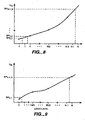
- An alternative method for determining the digital breakpoints between logic levels consists of programming tracking cells to non-adjacent logic levels. As long as the memory system knows in advance which logic levels are represented by the various tracking cells, the digital threshold breakpoints between logic levels may be determined without having to program tracking cells to every logic level. In this method, some assumption is made about the shape of the curve of the threshold vs. logic level. For example, Figure 7 shows such a system in which, here, a linear relation is assumed between the thresholds and the logic levels. In this case, linear interpolation is used to determine the threshold breakpoints between the logic levels.
- Figure 7 shows a threshold-logic level relation derived from just two points, 70 and 71, corresponding to a single pair of tracking cells, or more generally a pair of tracking cell populations. For simplicity, these two cells are taken to be associated with the lowest logic level, 0, and the highest logic level, N. (Equivalently, both here and in the rest of the discussion, the states could be ordered in reverse fashion, with "0" corresponding to the highest V th and so on.)
- the logic level corresponding to the tracking cells or tracking cell populations is established by the controller, firmware, or some combination of these at the time of data write.
- the corresponding V th0 and V thN is established by reading these cells, the V th vs.
- tracking cells or populations of tracking cells reduces the number of required tracking cells as well as the corresponding amount of overhead needed for these cells.
- Figure 7 used the highest and lowest logic states, these are generally not the preferred choice.
- One reason for not using these states is that they are relatively far, in terms of threshold values, from the intermediate logic states and therefore do not reflect these values as accurately. If the tracking cells instead correspond to a pair intermediate logic levels, at, say, roughly a quarter and three quarters of the way between the highest and lowest level, the average distance between the pair of logic levels corresponding to the tracking cells and the other logic levels is reduced. This will consequently result in better margins for the read process.
- these cells are re-programmed each time the user cells of the associated write block are written, preferably at the same time, using the same fixed, global reference levels to set the tracking and user cell programmed thresholds.
- These verify reference can be produced, for example, by band-gap voltage reference generators or other standard techniques. These can be used to generate all of the needed reference voltages, or else a fewer number with the other needed levels supplied by the same algorithm that produces the read break points from the tracking cells, as is described in more detail below with respect to analog examples.
- the threshold voltages of the tracking cells are also preferably read every time the user cells are read, and these thresholds are used to determine the stored logic levels of the user cells.
- Figure 7 assumes a linear relation between logic levels and their correspond threshold values.
- the actual shape of the V th vs. logic state curve will depend both upon how the cells are programmed and how they maintain this programming level over time and in varying read conditions.
- cells are programmed in a program/verify cycle which uses a series of program verify levels which are uniformly spaced, resulting in a linear relation at the time and conditions that programming is completed.
- Non-linearities may result when the verify levels differ from their nominal values.
- a non-linear relation could intentionally be introduced to exploit, for example, a known voltage dependent aging property of the cells or to compress the number of states stored in more stable portions of the available threshold window. Such intentional non-linearities can be compensated for by the V th vs. logic state curve, and can be computed in the controller or more directly as described below with respect to analog embodiments.
- each population of tracking cells associated a particular logic level consists of a single cell.
- multiple tracking cells are used in each population, with each of the populations programmed to one of two or more logic states.
- the advantages of using multiple tracking cells associated with a given logic level are discussed in U.S. patent no. 08/910,947 , 6,222,762 This method allows for the inevitable non-ideal threshold levels of the tracking cells as shown in Figure 10 , where two populations of 16 cells each are used. Mathematical regression methods may then be used to determine a best fit of the threshold vs. logic level curve.
- the two populations of tracking cells associated with logic levels 4 and 12.
- the threshold values in each population can then be averaged in a number of ways, for example a mean, weighted mean or mean with outlying values neglected, or a root mean square or mean based on other powers. From the average of each population, the linear relation can then be extracted. Alternately, rather than averaging the individual populations first, a least squares or other regression could be performed using all of the tracking cells, this being a distinct process if populations associated with more than two levels are used.
- a "bad" tracking cell which fails to program properly, this can either be mapped to an alternate cell in the same way as is done with the user data cells, or, more simply since it contains no user data, just switched out of the population. For example, if upon initial testing, a tracking cell fails to have a threshold around a test state, the defecting cell can be switched out by the supplier. Additionally, if the cell fails to verify properly during a program or erase operation, it can be switched out at that time. Furthermore, even among the "good” tracking cells, some may be ignored: For example, there may be a tracking cell, again such as that indicated by 101 in Figure 10 , which cannot be identified as "bad", but whose threshold will be substantially different from other tracking cell due to, say, overshoot in programming.
- this "good" tracking cell with a "bad” value can also be removed by ignoring any tracking cells in the calculation of breakpoints whose threshold voltage is a certain distance away from the average threshold voltage of all the tracking cells programmed to the same level. This distance could be a bound based on either a relative difference or absolute difference in the threshold value of the cell.
- the populations of tracking cells may be associated with only a subset of the total number of logic states.
- the example of Figure 10 has only two populations for the 16 possible logic states to which a user cell can be programmed. The result is that the generic breakpoint for distinguishing between a pair of logic states is not determined by the threshold voltages of the logic states between which it differentiates. For example, the breakpoint BP 5,6 is determined by populations associated with neither of logic states 5 and 6.
- the actual threshold voltages of the tracking cells can be used to translate the threshold values of the user cells back into data values in a number of ways, both analog and digitally based.
- the full m bits of the threshold information for the tracking and for the user cells is off-loaded to the processing circuit, which does the m to n bit translation.
- both the tracking and user cells could be read to 7-bit accuracy, the breakpoints determined, and the threshold values of the user cells converter to data values.
- only the tracking cells could be read to 7-bit accuracy, their values converted to 4-bit breakpoint voltages, and the user cells read directly with these 4-bit breakpoint voltages to determine their data content.
- the translation transform becomes essentially a straight line fit with a slope and intercept established by two sets of tracking cells, each set at some optimum state to minimize the error of such fitting.
- tracking cells associated with more than two states may be needed. In the extreme case, this would require each state to be represented. In order to keep the corresponding overhead increase under control, this would suggest reducing the number of cells per population associated with a state. In most applications, this extreme case is unlikely. It may be, however, that using 3 or 4 different state populations, such as is shown in Figures 8 and 9 , provides a reasonable compromise between the two limits.
- the processing associated with establishing the translation can take place in several different places. In the one option, this can occur within the controller, in which case the digitized threshold values of the tracking cells need to be shifted out from the memory to the controller with the full resolution available at the outset of the read to establish the translation. The remainder of the data can then be shifted out at this same resolution and have the controller process this data using the translation to extract the 4-bit data per cell, which, for a given I/O bus width and clock frequency, reduces the information transfer rate and increases power consumption. Alternately, the translation terms can be shifted back to the memory, for example filling up an on-chip fast look-up table RAM and used to process the remaining data on the memory chip.
- the translation can be done at the same time as shifting out the data, thereby shifting out only the 4-bit data of interest and minimizing loss of read speed and reducing the power associated with this data shifting.
- Another option is to perform the translation on the memory chip itself, by placing the controller on the same chip, and/or by establishing what associated voltage best satisfies the population of tracking cells associated with each predetermined state in a first pass sensing session, and from these values adjusting the full set of voltages used to read the 16 levels from the user cells in a second sensing session. Placing the controller on the same chip as the memory cells results in a savings in both time and power as it avoids the transfer of data on an input/output bus.
- FIG 11 is a block diagram of an example where the user cells are read directly with analog voltage levels derived from the tracking cells. Although many of these details will also apply to the digital implementations above, in the analog examples the threshold voltages of the tracking cells are not converted to digital values, but used in their analog form to set the read voltages directly for translating the threshold voltages of the user cells into data. Each data sector within the memory is preferable provided with such a circuit.
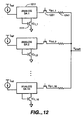
- a first set of L tracking cells TC 1,1 1111 to TC 1,L 1112, are connected to an averaging circuit AVE A 1110.
- a second averaging circuit AVE B 1120 is connected to a second population of tracking cells, here taken to also have L elements.
- the two averaging circuits determine the two voltages V aveA and V aveB associated with two of the logic levels from which the various read points are determined. In the more general case where populations associated with more than two logic levels are used, there would be one such averaging circuit per population.
- the V ave s are then supplied to the circuit 1130 for establishing the read points used to translate the user cell's threshold voltages into data.
- circuit 1130 may receive several other inputs. Since the states A and B to which the two populations correspond is rotated to provide a more uniform history, circuit 1130 determines which population corresponds to which level. For example, in an example corresponding to Figure 10 , one of these corresponds to logic level 4 and the other logic level 12. To determine which is which, circuit 1130 can either just directly compare these voltages, or else this information can be supplied by the controller, firmware, or wherever this information has been stored as a control signal, here labelled ROT. More generally, this could also contain information about changes in how these populations are associated.
- ROT control signal
- V PVhi and V PVlo global fixed program verify voltages, corresponding to each of the logic levels associated with the two populations are also supplied.
- a control signal, here called PGM is then used to decide whether the V ave s or the V PV s are used to set the read points.
- the read points are then supplied to READ/VERIFY circuit 1140. This can consist of only supplying the particular read points used for the operation then in process, for instance the breakpoints for data extraction, or else a larger number of sets of the voltages described with respect to Figure 14 can simultaneously be supplied. These read values are then used for the various read operations performed on the user data cells. Here, a single cell 1150 is shown to indicate the whole read sector with which the circuit of Figure 11 is associated. The circuitry of READ/VERIFY circuit 1140 then uses the read points to extract the data from the cell, for example by applying the various breakpoints to the control gate and monitoring the result with a sense amp as in the simplified arrangement of Figure 6 .
- the other averaging circuit are similarly constructed.
- Each of the tracking cells TC 1,1 -TC 1,16 are constructed and programmed similarly to the user memory cells. These are each connected to a respective analog sense amp, each fed by the same reference current I ref .
- tracking cell TC 1,1 1111 is connected to analog sense amp SA1 1211.
- the sense amp outputs the threshold voltage of V th1,1 of tracking cell TC 1,1 .
- each sense amp After passing across resistor 1241, this voltage is then combined with the other threshold voltages V th1,2 -V th1,16 to produce the average value of the tracking cells associated with the logic level A, V aveA .
- the output of each sense amp also passes through a transistor such as 1231 for analog SA 1. This is a provision for switching out any "bad" tracking cells. If, for example, the tracking cell is found to not program properly during initial testing, the chip provider can use transistor 1231 to remove the tracking cell from the population. Alternately, if a tracking cell fails to verify when written or erased at some later date, it can be switched out at that time.
- FIG. 12 provides a dedicated sense amp for each tracking cell
- alternate examples could allow tracking cells to share sense amps if the appropriate switching circuitry were provided.
- a tracking cell population consists of a single cell, only the single threshold voltage is supplied and the averaging is not needed.
- FIG. 13 One example of an analog sense amp connected to its tracking cell is shown in Figure 13 .
- a reference voltage V ref from band-gap voltage reference generator or other source is applied to the control gate of transistor 1301 to provide the reference current I ref to the sense amp 1211, producing a current to the source of tracking cell TC 1111.
- a pair of p-cascode devices, 1311 and 1312, followed by a second pair of cascode transistor, 1321 and 1322, with respective cascode biases are interposed between the tracking cell and transistor 1301.
- a node N1 is between the two set of cascode devices and is connected to the control gate of a transistor 1330.
- a second node N2 is connected to the control gate of the tracking cell 1111.
- the transistor 1330 will act like a source follower and set the voltage at N2 to the same level as the threshold voltage of the tracking cell, V th1,1 .
- the pair of cascode devices on either side of node N1 are used to boost the gain of the feedback loop.
- FIG 14 is a particular example of the read point circuit 1130 of Figure 11 .
- the voltages V aveA and V aveB are received at a switching circuit such as 1402. Since, as described above, it is often preferable to rotate the tracking cell populations between the logic states with which they are associated, the V ave s need to be connected according to which state they currently associated. For the case of two values, a simple circuit such as 1402 will connect V aveA to V aveHI and V aveB to V aveLO if the control signal ROTAB is de-asserted, and rotate these two connections if ROTAB is asserted.
- This correspondence between tracking cell populations and the logic levels is determined in a rotation determination circuit, shown here as block 1401.
- the inputs are the various V ave s, one or more signals containing the correspondence from the controller or wherever this information is stored, or a combination.
- block 1401 could determine the correspondence simply by comparing the values of the V ave s with one another. For example, in Figure 14 by asserting or de-asserting ROTAB based on whether V aveA >V aveB . Alternately, ROTAB could come directly from ROT.
- the additional control signals, CS i allow for changing the set of states with which the tracking cells are associated. In the simplified example without rotation, circuit 1402 would be absent and the averaged values would be applied directly to the corresponding node or op-amp.
- V ave s are then used to set the voltages of their corresponding logic levels in a chain of resistor elements. Rather than apply V aveHI and V aveLO directly to their corresponding node, they are connected to a corresponding op-amp, respectively 1421 and 1422, which act as buffers. Ignoring for a moment transistors 1431-1436, consider the second input of these op-amps as connected directly to respective nodes Y and X. In Figure 14 , the pair of tracking cell populations are associated with logic levels 3 and 13 when connected to nodes X and Y. Each logic state i then corresponds to the node above resistor R i . If the resistors R 0 -R 15 are all equal, a linear relation such as is shown in Figure 10 will result. Any variations in the resistance values, whether intentional or due to process variations, will produce a non-linear relation unless compensated for elsewhere.
- a set of transistors such as 1431-1433 and 1434-1436, can be included.
- a set of control signals here shown schematically as CS a -CS c
- the higher logic level associated with a population of tracking cells can be taken logic level 12, 13 (at the node Y), or 14.
- Circuit 1401 would then supply the signal to turn on the appropriate transistor, the others being off.
- the lower level is set in a similar manner using transistors 1434-1436 and signals CS d -CS f .
- the same read point circuit can be used for program verify (and any other read operations) as is used for data extraction.
- the input to op-amps 1421 and 1422 are connected to V aveHI and V aveLO , the node above each resistor R i is at the voltage V ave i , taken to the average threshold value of the logic state i for translating V th of a user data cell to a logic level at the time of data extraction.
- these nodes correspond to levels of the logic level when they are verified into a programmed state at the end of a write cycle.
- the same resistor chain is used to program both the user and tracking cells in a sector. For example, at the end of programming, if one of the tracking cell populations is associated with logic state 3, both the cells of this population and user cells programmed to this logic level will correspond to the node X.
- a switch is provided to connect either the V ave s or the V PV s to the appropriate op-amp.
- This is just shown schematically in Figure 14 as the pair of switches S H 1411 and S L 1412, which can be implemented by any of the standard arrangements and would operate together, with S H and S L respectively connected to V aveHI and V aveLO for data translation reading and respectively connected to V PVhi and V PVlo for program verify reading.
- Switches S H 1411 and S L 1412 would then be operated in response to an appropriate control signal, such as the program signal PGM indicated in Figure 11 , which would connect the resistor chain with the verify voltages when asserted and with the V ave s when de-asserted.
- V PVhi and V PVlo would be the global, fixed voltage reference values used for read verify during programming, generated by band-gap voltage reference generators on the chip or other standard techniques.
- non-linearities introduced into the V th vs. logic level relations during programming are automatically compensated for when translating the threshold values back into logic states. This occurs whether the non-linearity is intentional or not. For example, device mismatches due to process variation can produce a non-uniform spacing of threshold ranges; however, as the same mismatches occur when translating back the user cells to logic level, this effect is largely undone. Alternately, a design choice may be made to pack states more densely into, say, the lower portion of the threshold window. This can be accomplished by taking the values of the resistors on the bottom of end of the chain to a smaller values than those at the top.
- the non-linearity is then automatically introduced during programming and removed during reading without the sort of loss in performance a computational implementation would introduce.
- the same device is used on the drains of both reference cells and data cells for their respective analog sense amps and read sense amps, with the same current mirrors used for the reference currents.
- Figure 14 is a detail of Figure 14 showing one of the resistors R i and where it is tapped to provide the various values used.
- Each resistor R i is broken up into a sub-chain of resistors, here taken to be eight resistors R i ,0 -R i ,7 , to provide the breakpoint read points and other intermediate values used in reading processes.
- the breakpoint BP i ,( i -1) is set midway between what is taken as the average values taken for the threshold voltages of the states i and ( i- 1), V ave i and V ave( i -1) .
- Other read points are pulled off in the same way.
- a low marginning value for the state i and a high marginning value for the state ( i -1), V ml i and V mh( i -1) respectively, are shown as lying on the node just above and below that of BP i ,( i -1) . How close the margining values are taken to the corresponding V ave value will determine how tightly the distribution is clustered about this value when written.
- the number of nodes is determined by the amount of resolution desired and the number of distinct sorts of read points desired, such as the various read points described in U.S. patent number 5,532,962 .
- the resistors R i ,0 -R i ,7 of the sub-chain can be taken with non-equal values if a non-uniform spacing of the node values is wanted.
- tracking cell are programmed in the same manner as the user data cells. These reference cells are then written with the same algorithm as the user cells, using programming pulses of the same intensity, with the same duration, and verified at the same level. Although this produces similar histories and distributions for both the tracking cells and the user cells, in some applications an embodiment of the present invention that programs the tracking cells differently may be used.
- Writable reference cells have uncertainty in their written threshold values. When using this threshold to determine the logic level to which a user cell has been written, this uncertainty is a significant probabilistic error term. For example, consider the scenario where the written threshold uncertainty for storage cells may be 105mV. If the reference cells have the same 105mV uncertainty, then the voltage difference between a storage cell and a reference cell may be as high as 105mV. If the voltage separation between levels is 200mV, then there will be storage cells that will have thresholds closer in value to that of a reference cell for an adj acent logic level than to that of the reference cell for the appropriate logic level. This will cause a read error on such storage cells.
- the written threshold uncertainty may be reduced by taking more time to write all reference cells and user cells. For example, shorter write pulses may be used. This results in a smaller threshold change for each write pulse, and therefore a finer resolution (less uncertainty) in the final threshold.
- this scheme implies that the cell is being checked against the target threshold more often, meaning more time is being taken for the read operations. This reduces the overall write speed, which may not be an acceptable tradeoff for some applications such as streaming video storage.
- a lower control gate and/or drain voltage is used for reference cells than for user storage cells.
- Lower voltages reduce the programming speed for most non-volatile memory cell writing operations. If the same timing is used as for user storage cells, then the average reference cell undergoes less threshold change than the average user cell for the same amount of write time.
- the write algorithm consists of multiple write pulses, with intervening comparisons of the cell threshold to a final target value. Therefor writing cells more slowly with less threshold change per write pulse results in less uncertainty in the final threshold.
- the slowest writing reference cell can usually complete writing to the target level as quickly as the slowest user cell.
- the reference cells may be written about twice as slowly as the user cells, and consequently to about two times better resolution, without impacting the overall required write time for the total cell population.
- the same voltages may be used for programming the user cells and reference cells, but different write timing may be used for the reference cells. Specifically, if shorter write pulses may be used for the reference cells, then they may be written to a better resolution.
- the verify time is 20% that of the write time.
- T pu the total write plus verify time to be the same for the slowest user cell and slowest reference cell.
- Total time ( write + verify ) for tracking cells T pu + 0.2 ⁇ T pu ⁇ M
- T pref the reference cell write pulse width and M is the number of write pulses required for the slowest reference cell.
- write time required for slowest user cell T pu ⁇ N
- write time required for slowest reference cell T pref ⁇ M .
- the reference cells may be written to 7.7 times better resolution.
- user cell threshold uncertainty is 105mV
- the defective reference cell can either be mapped to a new cell or simply removed from the population as it contains no user data.
Abstract
Description
- The present invention relates generally to non-volatile semiconductor memory devices and, more particularly, to the use of tracking cells.
- In a semiconductor memory cell, data is stored by programming the cell to have a desired threshold voltage. The data stored in the cell is read by determining the threshold voltage of the cell and translating this voltage to a logic level. For a two state, binary memory cell, this translation can be done by use of a reference or breakpoint voltage to provide a read point: cells with a threshold voltage above this read point correspond to one state, while those with a threshold voltage below this read point correspond to the other state. When a memory cell is a multi-state cell, a number of such read points need to be introduced to distinguish between the states.
- As the number of states stored in a memory cell increases, more states must be contained within a range of threshold values. Consequently, the portion of this range corresponding to a given state become ever narrower and the read points become ever closer. Once the memory cells have been programmed, their threshold values may change from the level to which they were programmed for a number of reasons. This can be due to the less than perfect charge retention in non-volatile memories, where a cell's threshold may go up or down depending on applied bias voltages, fields generated by the stored charge itself, and charge trapped in dielectrics. It can also be due to changes in operating conditions between when the cell is programmed and when it is read. If the read points used to determine the data content of the cells do not follow these changes in the cell, the read points will no longer accurately discriminate between the different threshold voltages. This is the case when a fixed, global set of reference voltages, such as from a band-gap circuit, is used to produce the read points. Such a circuit will not respond, or respond differently, to the conditions which lead the threshold voltages of the memory cells to change. When this change becomes large enough, the read points will no longer accurately discriminate between the threshold voltages found on the cells and the data programmed can no longer be accurately read.
- One method to improve the accuracy of the correspondence between the read points and threshold voltage of the cells programmed to a particular data state at the time these cells are read is the use of writable reference or tracking cells. These are a set of memory cells, but which are not written with data and instead are written to predetermined reference values. The read points are then extracted from these cells, which, as they will behave similarly to the data cells, will provide a more accurate correspondence between a data level and the current threshold voltage of a cell originally programmed to that level. The use of reference cells in multi-state memories are described in
U.S. patent 5,172,338 and further developed inU.S. patent no. 6,222,762 . - Reference is also made to prior art
patent application US 5,608,679 relating to fast internal reference cell trimming for Flash EEPROM memory. - As the number of states per cell continues to increase, further improvements in the accuracy of the reading process will be needed. Therefore, improvements in tracking cell techniques are needed which not only increase their accuracy and speed of use, but also decrease the amount of overhead they require, both in terms of the actual tracking cells and also in terms of the related circuitry.
- The present invention provides a non-volatile memory according to
claim 1 and a method of operating a non-volatile memory according to claim 10. - The present invention provides for using different voltages and/or timing for the writing of tracking cells to provide less uncertainty in the tracking cells' final written thresholds. Since there are typically many fewer tracking cells than user storage cells, system write speed is most often limited by the user cells, not the reference cells. Therefore, it may be possible to use different voltages and/or timings which write the reference cells more slowly on average while still writing the slowest reference cell as quickly as the slowest user cell. This can reduce reference cell threshold uncertainty without significantly effecting the overall system write speed.
- Additional objects, advantages, and features of the present invention will become apparent from the following description of its preferred embodiments, which description should be taken in conjunction with the accompanying drawings.
-
-
Figure 1 shows a relation between tracking cell thresholds and those of the user cells. -
Figure 2 is a block diagram of an analog arrangement of differential sensing used directly to compare individual tracking cell thresholds to user cell thresholds. -
Figure 3 shows an alternate relation between tracking cell thresholds and those of the user cells. -
Figure 4 is a schematic representation of an arrangement of differential sensing using multiple tracking cells. -
Figure 5 shows a range of control gate voltages spanning the entire range of the expected cell threshold values. -
Figure 6 is a block diagram of an arrange for using the levels ofFigure 5 to determine the cell thresholds. -
Figure 7 shows such a system in which a linear relation is assumed between thresholds and logic levels. -
Figure 8 shows tracking cells programmed to three different logic levels to allow extraction of a non-linear relationship between threshold and logic level. -
Figure 9 shows four logic levels used to allow extraction of an even more complex non-linear relationship between threshold and logic level. -
Figure 10 shows multiple tracking cells associated with a given logic level. -
Figure 11 is a block diagram of an example where the user cells are read directly with analog voltage levels derived from the tracking cells. -
Figure 12 is a detail ofFigure 11 showing an example of thecircuit AVE A 1110 and its tracking cells in more detail. -
Figure 13 shows an example of an analog sense amp connected to its tracking cell. -
Figure 14 is a particular example of the read point circuit ofFigure 11 . -
Figure 15 is a detail of one of the resistors R i inFigure 14 showing where it is tapped to provide the various values used. - The storage capacity of non-volatile semiconductor memories has increased both by the reduction in size of the individual components of the circuits and by increasing the amount of data storable in an individual memory cell. For example, devices such as those described in U.S. patents 5,712,189, 6,103,573 and 6,426,893 and
U.S. patent no. 6,512,263 which are all assigned to SanDisk Corporation can store upwards of four logical bits per physical floating gate storage transistor. This storage will require each floating gate to be able to have encoded within it one of the sixteen or more possible memory states. Each one of these memory states corresponds to a unique value, or, more accurately, a narrow range of values, of stored charge on the floating gate which is sufficiently separated from its neighboring states' charge storage values to clearly differentiate it from those neighboring states as well as the other states. - The determination of a cell's stored charge level can be performed by current sensing, where the magnitude of its conduction using fixed bias conditions is sensed, or through threshold voltage conditions, where the onset of such conduction is sensed using varied steering gate bias conditions, to give two of the more standard arrangements. Current sensing approaches are more fully developed in
U.S. patent nos. 5,172,338 and6,222,762 and may be employed with the various examples described below. However, the majority of the following exposition uses the threshold voltage, Vth, sensing approach as this improves the sensing resolution, keeps the current, and consequently the power, associated with massively parallel read operations low, and minimizes vulnerability to high bit line resistance. - The actual sensing can be performed in several ways, for example by comparing a cell's threshold voltage to each of the reference values in order. For multi-state cells, it can be more efficient to exploit a cell-by-cell, data conditional binary search, which, for example, is capable of determining, in parallel, each sensed cell's Vth to a one in sixteen resolution through a sequential, four-pass sensing operation. The amount of resolution required for sensing is discussed below with respect to the various examples presented. As usual, the amount of resolution used is often a tradeoff between higher resolution, resulting in more potential "bits" beyound the minimum required 4-bit resolution of the exemplary examples, but at the cost of more area, to sense and store these extra bits, as well as more time consumed, both due to the additional sensing passes in the binary search of these extra bits and due to transferring this extra information.
- To extract the data stored in the memory cells, this data must be both written and stored with sufficient fidelity. At the time of programming, the range of values associated with each storage state within the data unit being written, such as a sector, should be confined to a consistently tight range, and the separation between the center of each of these ranges and their associated nearest neighbors, that is, the states with a Vth adjacent just above and below, within the unit being written can also be maintained within a constantly controlled target range. Once the data is written, the stored charge levels within the population of cells will, to first order, maintain their levels over time, with drift from these values in a common mode being a second order effect and dispersion being even less significant.
- When reading a data unit, the storage state of each of the cells within that unit should be resolved by the sensing circuitry with a sufficiently high precision and resolution to adequately resolve the range of each storage band and the separation between each of the adjacent bands. It should be noted that this does not require that the user data associated with each of these states is known, merely that the states contained therein are read back with sufficient fidelity. Those cells which can not be read, or, alternately, be programmed or store data, with sufficient fidelity can be treated with error correction code (ECC) or other equivalent error management, such as is described in
U.S. patent 5,418,752 . - Under these arrangements, the minimal requirements of sensing are that it only needs to resolve each cell's storage with sufficient fidelity. In this way it is able to recreate the level relationship each cell has with all the other cells within the concurrently written storage unit or sector. It is not essential that the absolute data that these values represent be established at this time, as long as there can be extracted from this information a key or translator to provide such a mapping or discrimination filter between the resolved storage levels and the corresponding states. In the absence of such a key, this imposes the additional requirement of absolute referencing to recreate with sufficient precision the exact operating conditions present at the time the data was originally written in order to allow an accurate translation of the levels to data. Any inaccuracy in such translation must be guard-banded, increasing the margin requirements of the states and consequent memory window. Since a memory window of usable threshold voltages is of limited size, due to reliability and dynamic range considerations, this would limit the number of levels encodable and, consequently, the number of physical bits stored in a physical memory cell.
- Even given such an absolute reference capability, in the case where, when read at some time in the future, there is a common mode shift in the read back levels relative to the levels established at the time of the original write, as could occur at high write cycle endurance levels which are vulnerable to "relaxation" due to cell detrapping, such absolute referencing does not help---the translation between levels read back and data is no longer the same. Given this, plus the very difficulty in guaranteeing such absolute referencing capability in volume production, over years of data storage and operation, wide ranges of operating temperatures, and the various target supply levels and associated ranges that end products may be expected to satisfy, it is often preferred not to depend on such "absolute" referencing, but rather to depend on "relative" capabilities inherent in the storage medium.
- This can be accomplished by burying the translation key within the medium, often within the data sector unit itself. In the examples below, an additional number of physical cells, overhead reference or "tracking" cells, can be introduced within each sector to support this function, such as described in
U.S. patent 5,172,338 and6,222,762 . . For most examples, these cells are, in all respects, the same as the user data cells, except they contain known data or storage levels established by the controller, firmware, or some combination of these at the time of data write. They can be attached to the user data in a way analogous (as far as location and programming, although not in function) to ECC bits, as described inU.S. patent 5,418,752 . Each data sector then contains both the user data cells, but can also contain the tracking cells, the error correction code cells, header, and so on which are not directly used for storing data. In examples with both tracking cells and ECC cells, both can used to increase reliability of the memory in a complementary manner, with the ECC cells used to correct the data values and the tracking cells used to read both the user data and ECC cells. - In most of the examples described, the tracking cells are treated the same way as user data cells, benefiting from rotation and any other wear leveling strategies, so that most accurately reflect the history of their associated user data designated cells. The rotation of user data can be tied to the rotation, or toggling, of tracking cells as described below, or else treated independently. Since the tracking cells' rotation information can be extracted by comparing their threshold levels, the rotation of user cells can then be determined from the tracking cell rotation. As the tracking cell rotation can be treated as a function of the user cell rotation, by correlating this information, the memory can save on overhead since extra cells need not be allocated to store user cell rotation information. The description below gives several variations on the use of writable tracking cells which can be used, either individually or in conjunction, to improve upon the methods of
U.S. patent 5,172,338 and no. 6,222,762. - By reprogramming the tracking cells each time the associated user cells are programmed, the tracking cells develop the same history and therefore the same charge retention characteristics as the user cells. For example, if user cells' thresholds drop on the average by 10mV after 10 years, the tracking cells' thresholds will on average drop by the same 10mV. By reading the tracking cells at the same time as the user cells and using the tracking cells to determine the expected threshold voltages for each logic level, this charge loss does not degrade the effective margin of the user cells.
- Also, it is well know that non-volatile memory cells' charge retention characteristics change as a function of the number of program/erase cycles performed. By having tracking cells erased and reprogrammed roughly the same number of times as the user cells, this cycling dependence on charge retention is also accounted for and does not reduce the effective cell threshold margin.
- The threshold of tracking cells may be read using either analog or digital techniques. One example of an analog technique includes programming the tracking cells to thresholds between those of the user cells in one of N=2n states, as illustrated schematically in
Figure 1 . (BothFigure 1 and Figure 3 , below, are idealizations where all of the cells are in one of a number of individual values instead of the more realistic ranges of values.) In this case differential sensing may be used directly to compare individual tracking cell thresholds to user cell thresholds with the same control gate voltage, VCG, applied.Figure 2 shows a block diagram of such an analog arrangement, with VCG applied to both theuser cell 22 and a trackingcell 21 that distinguishes between level i and i+1, the output of both cells being fed todifferential amplifier 23 to determine if Vth of theuser cell 22 is above or below that of trackingcell 21. By comparing the user cells to the tracking cells programmed to various levels, the logic state of the user cells is determined. These comparisons may be a linear search, comparing each cell to each tracking cell, or a binary search, reducing the number of comparisons required. - Another method using analog sensing of the tracking cells to be programmed to the same thresholds as those of the user cells, as illustrated schematically in
Figure 3 . In this case, during the read operation multiple tracking cells are used to determine the appropriate control gate voltages for reading the user cells, as shown inFigure 4 and developed more fully inU.S. patent no. 6,222,762 . Here thetracking cells SA 43 andSA 44 feed back to the cell control gates in a manner such that the output of the sense amplifier is the threshold of the tracking cell. Multiple sense amplifier outputs are then input to a circuit,V AVERAGE 45, which determines the appropriate intermediate control gate level for reading the user cells, here represented by thesingle cell 46.Sense amp SA 47 then determines whether the threshold voltage of theuser cell 46 is above or below this intermediate value, as indicated by theoutput 0/1. InFigure 4 , the appropriate control gate voltage foruser cell 46 is an intermediate value between the threshold voltages of the two trackingcells - Other methods for using tracking cells involve reading multiple digital values for the tracking and user cell thresholds, then using digital processing techniques to determine the user cells' logic level are described in
U.S. patent no. 6,222,762 will now be more fully developed. One such method starts by programming tracking cells to the same thresholds as those of the user cells, as inFigure 3 . A read operation then consists of applying a series of fixed control gate voltages, VCG, to the tracking cells and simultaneously to the user cells. As shown schematically inFigure 5 , these control gate voltages span the entire range of the expected cell threshold values. By applying a series of control gate voltages VCG such as indicated inFigure 6 , digital values representing the cell's thresholds are determined. For example, if 16 different control gate voltages are available, a log2(16)=4 bit digital value may be determined. If a 7 bit value is desired, than 27=128 different control gate voltages are required. As above, these control gate voltages may be applied in a linear sequence or in a binary search fashion. The number of bits, m, used to read and store the threshold value must be at least as large as the number of logical bits of information stored in each user memory cell, n. - (Alternately, rather than varying the control gate voltage, the sense amp trip current may be altered to determine some or all of the digital bits representing the cell threshold. Current based reading techniques are discussed, for example, in
U.S. patent 5,172,338 . However, when the number of multi-states storable on a given floating gate becomes large, the voltage based techniques are often preferred for the reasons stated above.) - In
Figures 4a and 4b ofU.S. patent no. 6,222,762 , the case of 4-level and 8-level, respectively corresponding to n=2 and n=3, are shown in some detail. These figures correspond to a more fully developed version ofFigure 5 , where the states are shown to correspond to a distribution of threshold values and margin values are included. In particular, the 4-state cell with 7-bit resolution, corresponding to n=2 and m=7, is developed. The n=4, N=16 state cell of the exemple here will also be discussed in terms of an m=7 resolution. - Once these digital values are determined, they are used to determine the stored logic levels of the user cells. One method consists of calculating the digital midpoints between the threshold values of the tracking cells programmed to adjacent threshold states. For example, one tracking cell programmed to logic level i may have a digital threshold value stored as 0001110. Another tracking cell programmed to logic level i+1 may have a digital threshold value stored as 0001010. The digital midpoint between these two values is 0001100. Therefore all the user cells with threshold values read as greater than 0001100 are determined to have â logic level of i+1 or higher. All the user cells with threshold values less than 0001100 are determined to have a logic level of i or lower. By repeating this process with multiple sets of tracking cells, the specific logic level of each user cell may be determined.
- An alternative method for determining the digital breakpoints between logic levels consists of programming tracking cells to non-adjacent logic levels. As long as the memory system knows in advance which logic levels are represented by the various tracking cells, the digital threshold breakpoints between logic levels may be determined without having to program tracking cells to every logic level. In this method, some assumption is made about the shape of the curve of the threshold vs. logic level. For example,
Figure 7 shows such a system in which, here, a linear relation is assumed between the thresholds and the logic levels. In this case, linear interpolation is used to determine the threshold breakpoints between the logic levels. -
Figure 7 shows a threshold-logic level relation derived from just two points, 70 and 71, corresponding to a single pair of tracking cells, or more generally a pair of tracking cell populations. For simplicity, these two cells are taken to be associated with the lowest logic level, 0, and the highest logic level, N. (Equivalently, both here and in the rest of the discussion, the states could be ordered in reverse fashion, with "0" corresponding to the highest Vth and so on.) The logic level corresponding to the tracking cells or tracking cell populations is established by the controller, firmware, or some combination of these at the time of data write. The corresponding Vth0 and VthN is established by reading these cells, the Vth vs. logic level curve determined to provide the threshold voltages of the states, and the logic level differentiating break points, BPi,i+1, along with any marginning values are extracted. For examples differentiating between the "0", or ground, logic state and a lower, post-erasure "erased" state, an additional breakpoint BP0,e would be included below Vth0. - Using fewer tracking cells or populations of tracking cells than the number of states reduces the number of required tracking cells as well as the corresponding amount of overhead needed for these cells. In the exemplary 4-bit example, the use of tracking cells associated with only two states results in a factor of 8 reduction in the number of tracking cells compared to using cells associated with each of the 24=16 states.
- Although
Figure 7 used the highest and lowest logic states, these are generally not the preferred choice. One reason for not using these states is that they are relatively far, in terms of threshold values, from the intermediate logic states and therefore do not reflect these values as accurately. If the tracking cells instead correspond to a pair intermediate logic levels, at, say, roughly a quarter and three quarters of the way between the highest and lowest level, the average distance between the pair of logic levels corresponding to the tracking cells and the other logic levels is reduced. This will consequently result in better margins for the read process. - Another reason for not using the highest and lowest logic states is these do not correspond as well to a "typical" data cell. One of the motivations for using writable tracking cells is that the tracking will have a fairly typical history when compared with the user cells. To more accurately reflect the history of their associated user data designated cells, as well as provide a more accurate Vth vs. logic level relation, the use of logic states nearer the middle logic levels is generally more accurate. For example, if N=16, the states associated with, say,
logic levels state U.S. patent no. 6,222,762 and developed more fully inU.S. patent no. 5,270,979 . Thus, although the tracking cells are not rotated through all the possible logic state, by being rotated between being programmed to a relatively high and a relatively low Vth state, they will approximate the history of a typical user cell. - In most examples, these cells are re-programmed each time the user cells of the associated write block are written, preferably at the same time, using the same fixed, global reference levels to set the tracking and user cell programmed thresholds. These verify reference can be produced, for example, by band-gap voltage reference generators or other standard techniques. These can be used to generate all of the needed reference voltages, or else a fewer number with the other needed levels supplied by the same algorithm that produces the read break points from the tracking cells, as is described in more detail below with respect to analog examples. The threshold voltages of the tracking cells are also preferably read every time the user cells are read, and these thresholds are used to determine the stored logic levels of the user cells.
-
Figure 7 assumes a linear relation between logic levels and their correspond threshold values. The actual shape of the Vth vs. logic state curve will depend both upon how the cells are programmed and how they maintain this programming level over time and in varying read conditions. Typically, cells are programmed in a program/verify cycle which uses a series of program verify levels which are uniformly spaced, resulting in a linear relation at the time and conditions that programming is completed. Non-linearities may result when the verify levels differ from their nominal values. Alternately, a non-linear relation could intentionally be introduced to exploit, for example, a known voltage dependent aging property of the cells or to compress the number of states stored in more stable portions of the available threshold window. Such intentional non-linearities can be compensated for by the Vth vs. logic state curve, and can be computed in the controller or more directly as described below with respect to analog embodiments. - To lowest order, if the cells are programmed to a particular Vth vs. logic state curve, they will retain this curve. To higher order, with time and varying read conditions, cells with different threshold values will deviate by differing amounts. These effects can be compensated for by using a more complex curve. In
Figure 8 , tracking cells are programmed to three different logic levels, here taken as thestates 2, N/2, and (N-2). This allows extraction of a non-linear relationship between threshold and logic level. InFigure 9 ,4 logic levels are used to allow extraction of an even more complex non-linear relationship between threshold and logic level. In general, when more than two logic levels are used, the curve can either be constructed to be piece-wise linear, or else a curve of higher order. If taken to be piece-wise linear, it would be assumed linear between each pair of points, with the any needed extrapolation beyound the lowest and highest level tracking cells either just being a linear continuation or else based on some assumed behavior of cells near the "0" and "N" states. If K populations of tracking cells are used, each associated with a different logic level, a curve of up to order of (K-1) (or higher if assumptions are made on the boundary behavior) can be extracted. Alternately, a curve of order less than (K-1) could be formed using least squares, cubic splines, or other standard techniques. - So far, the examples presented have, usually implicitly, assumed that each population of tracking cells associated a particular logic level consists of a single cell. In other examples, multiple tracking cells are used in each population, with each of the populations programmed to one of two or more logic states. The advantages of using multiple tracking cells associated with a given logic level are discussed in
U.S. patent no. 08/910,947 ,6,222,762 This method allows for the inevitable non-ideal threshold levels of the tracking cells as shown inFigure 10 , where two populations of 16 cells each are used. Mathematical regression methods may then be used to determine a best fit of the threshold vs. logic level curve. - In the example of
Figure 10 , the two populations of tracking cells associated withlogic levels Figure 10 cut off) is typically the simplest and fastest implementation, with the computation involved in higher order curves requiring more processing. - In the event a "bad" tracking cell which fails to program properly, this can either be mapped to an alternate cell in the same way as is done with the user data cells, or, more simply since it contains no user data, just switched out of the population. For example, if upon initial testing, a tracking cell fails to have a threshold around a test state, the defecting cell can be switched out by the supplier. Additionally, if the cell fails to verify properly during a program or erase operation, it can be switched out at that time. Furthermore, even among the "good" tracking cells, some may be ignored: For example, there may be a tracking cell, again such as that indicated by 101 in
Figure 10 , which cannot be identified as "bad", but whose threshold will be substantially different from other tracking cell due to, say, overshoot in programming. During the processing of tracking cells, this "good" tracking cell with a "bad" value can also be removed by ignoring any tracking cells in the calculation of breakpoints whose threshold voltage is a certain distance away from the average threshold voltage of all the tracking cells programmed to the same level. This distance could be a bound based on either a relative difference or absolute difference in the threshold value of the cell. - For any of these methods, whether the populations of tracking cells consist of one or many points, these populations may be associated with only a subset of the total number of logic states. In particular, the example of
Figure 10 has only two populations for the 16 possible logic states to which a user cell can be programmed. The result is that the generic breakpoint for distinguishing between a pair of logic states is not determined by the threshold voltages of the logic states between which it differentiates. For example, the breakpoint BP5,6 is determined by populations associated with neither of logic states 5 and 6. - The actual threshold voltages of the tracking cells can be used to translate the threshold values of the user cells back into data values in a number of ways, both analog and digitally based. In one set of examples, the full m bits of the threshold information for the tracking and for the user cells is off-loaded to the processing circuit, which does the m to n bit translation. This processing circuit could be the controller which, depending on the example, is contained on another chip from the actual memory cells, or contained on the same chip. In addition to its other functions, such managing the memory and transferring data from the host system, the controller could then compute the linear or higher order Vth vs. logic state translation curve. Variations on this process for a 4 state user cells using m=7 bit resolution are presented in
U.S. patent application serial no. 6,222,762 , as noted above. For the present 4-bit user cell example, both the tracking and user cells could be read to 7-bit accuracy, the breakpoints determined, and the threshold values of the user cells converter to data values. Alternately, only the tracking cells could be read to 7-bit accuracy, their values converted to 4-bit breakpoint voltages, and the user cells read directly with these 4-bit breakpoint voltages to determine their data content. - As reading is a faster process that programming, reading at 7-bit accuracy while programming to 4-bit accuracy, based on the fixed global verify values, does not result in near the loss of speed that using 7-bit accuracy for both processes would produce. Particularly when the read process uses a binary search, the cost of 7-bit accuracy just for read is much less than losses that would come from a full 7-bit implementation.
- Given the above options, there a number of various examples using writable tracking cells in different ways and in different numbers. Given that the key objective is to establish the proper, or at least optimal, translation between measured states and stored data, the function of the tracking cells is to pin down this optimum translation.
- If the sensing circuitry maintains its linearity, or at least its consistency if not linear, then the translation transform becomes essentially a straight line fit with a slope and intercept established by two sets of tracking cells, each set at some optimum state to minimize the error of such fitting. Despite the capability to tightly confine a population of cells within any given state, since there is invariably some spread in any group, including the tracking cell groups, this suggests that there be a sufficient number of such cells to establish, statistically, the center of each population. In this way, guard-bands against errors associated with establishing the translation can be increased by as much as one-half of the spread. For example, if memory states are separated by two such full spreads (that is, a full spread is maintained as separation between the outer edges of each neighbors states' distributions), then a reference established from the center, or extremely near the center, will give the maximum margin to differentiate between that state and its nearest neighbor. If too few tracking cells are used in a population, then there is the chance of setting this reference value from close to the extreme of a population, robbing sensing margin equivalent to 25% of the state to state separation. The optimum number of cells is a trade off between overhead area, and consequently cost, versus precision; but even a relatively small population, ranging from 10 to 30 cells should be sufficient in many applications. The cost of such overhead per sector is relatively small. For example, in a write sector containing about 1024 user data cells, which at 4 bits or ½Byte per cell gives 512Bytes, the 16 cells in each of two tracking cell groups of
Figure 10 amounts to only around a 3% overhead area cost. - If, however, some non-negligible amount of varying distortion is inherent within the sensing operation, such that there are non-linearities in the transformation that are different between the time of write and later reads, tracking cells associated with more than two states may be needed. In the extreme case, this would require each state to be represented. In order to keep the corresponding overhead increase under control, this would suggest reducing the number of cells per population associated with a state. In most applications, this extreme case is unlikely. It may be, however, that using 3 or 4 different state populations, such as is shown in
Figures 8 and 9 , provides a reasonable compromise between the two limits. - As already noted, the processing associated with establishing the translation can take place in several different places. In the one option, this can occur within the controller, in which case the digitized threshold values of the tracking cells need to be shifted out from the memory to the controller with the full resolution available at the outset of the read to establish the translation. The remainder of the data can then be shifted out at this same resolution and have the controller process this data using the translation to extract the 4-bit data per cell, which, for a given I/O bus width and clock frequency, reduces the information transfer rate and increases power consumption. Alternately, the translation terms can be shifted back to the memory, for example filling up an on-chip fast look-up table RAM and used to process the remaining data on the memory chip. The translation can be done at the same time as shifting out the data, thereby shifting out only the 4-bit data of interest and minimizing loss of read speed and reducing the power associated with this data shifting. Another option is to perform the translation on the memory chip itself, by placing the controller on the same chip, and/or by establishing what associated voltage best satisfies the population of tracking cells associated with each predetermined state in a first pass sensing session, and from these values adjusting the full set of voltages used to read the 16 levels from the user cells in a second sensing session. Placing the controller on the same chip as the memory cells results in a savings in both time and power as it avoids the transfer of data on an input/output bus.
-
Figure 11 is a block diagram of an example where the user cells are read directly with analog voltage levels derived from the tracking cells. Although many of these details will also apply to the digital implementations above, in the analog examples the threshold voltages of the tracking cells are not converted to digital values, but used in their analog form to set the read voltages directly for translating the threshold voltages of the user cells into data. Each data sector within the memory is preferable provided with such a circuit. - In
Figure 11 , a first set of L tracking cells,TC 1,1 1111 toTC 1,L 1112, are connected to anaveraging circuit AVE A 1110. A secondaveraging circuit AVE B 1120 is connected to a second population of tracking cells, here taken to also have L elements. Based on the threshold values of these tracking cells, the two averaging circuits determine the two voltages VaveA and VaveB associated with two of the logic levels from which the various read points are determined. In the more general case where populations associated with more than two logic levels are used, there would be one such averaging circuit per population. The Vaves are then supplied to thecircuit 1130 for establishing the read points used to translate the user cell's threshold voltages into data. - Besides the Vaves,
circuit 1130 may receive several other inputs. Since the states A and B to which the two populations correspond is rotated to provide a more uniform history,circuit 1130 determines which population corresponds to which level. For example, in an example corresponding toFigure 10 , one of these corresponds tologic level 4 and theother logic level 12. To determine which is which,circuit 1130 can either just directly compare these voltages, or else this information can be supplied by the controller, firmware, or wherever this information has been stored as a control signal, here labelled ROT. More generally, this could also contain information about changes in how these populations are associated. Since, as described below with respect toFigure 14 , thesame circuitry 1130 is also preferably used for program verify and other reading operations besides data extraction, global fixed program verify voltages, VPVhi and VPVlo, corresponding to each of the logic levels associated with the two populations are also supplied. A control signal, here called PGM, is then used to decide whether the Vaves or the VPVs are used to set the read points. - The read points are then supplied to READ/VERIFY
circuit 1140. This can consist of only supplying the particular read points used for the operation then in process, for instance the breakpoints for data extraction, or else a larger number of sets of the voltages described with respect toFigure 14 can simultaneously be supplied. These read values are then used for the various read operations performed on the user data cells. Here, asingle cell 1150 is shown to indicate the whole read sector with which the circuit ofFigure 11 is associated. The circuitry of READ/VERIFYcircuit 1140 then uses the read points to extract the data from the cell, for example by applying the various breakpoints to the control gate and monitoring the result with a sense amp as in the simplified arrangement ofFigure 6 . (The programming circuitry for the tracking and user data cells is suppressed here to keep these figures simplified to the elements being discussed, but is shown, for example, inU.S. patents 5,172,338 or5,418,752 , or6,222,762 .) -
Figure 12 shows an example of thecircuit AVE A 1110 and its tracking cells in more detail for the case of L=16. The other averaging circuit are similarly constructed. Each of the tracking cells TC1,1-TC1,16 are constructed and programmed similarly to the user memory cells. These are each connected to a respective analog sense amp, each fed by the same reference current Iref. For instance, trackingcell TC 1,1 1111 is connected to analogsense amp SA1 1211. Using the reference current Iref as an input, the sense amp outputs the threshold voltage of Vth1,1 of tracking cell TC1,1. After passing acrossresistor 1241, this voltage is then combined with the other threshold voltages Vth1,2-Vth1,16 to produce the average value of the tracking cells associated with the logic level A, VaveA. The output of each sense amp also passes through a transistor such as 1231 foranalog SA 1. This is a provision for switching out any "bad" tracking cells. If, for example, the tracking cell is found to not program properly during initial testing, the chip provider can usetransistor 1231 to remove the tracking cell from the population. Alternately, if a tracking cell fails to verify when written or erased at some later date, it can be switched out at that time. Although the example ofFigure 12 provides a dedicated sense amp for each tracking cell, alternate examples could allow tracking cells to share sense amps if the appropriate switching circuitry were provided. Of course, in the case that a tracking cell population consists of a single cell, only the single threshold voltage is supplied and the averaging is not needed. - One example of an analog sense amp connected to its tracking cell is shown in
Figure 13 . A reference voltage Vref, from band-gap voltage reference generator or other source is applied to the control gate oftransistor 1301 to provide the reference current Iref to thesense amp 1211, producing a current to the source of trackingcell TC 1111. A pair of p-cascode devices, 1311 and 1312, followed by a second pair of cascode transistor, 1321 and 1322, with respective cascode biases are interposed between the tracking cell andtransistor 1301. A node N1 is between the two set of cascode devices and is connected to the control gate of atransistor 1330. Between thetransistor 1330 and atransistor 1340 connected ground and controlled by a bias current, a second node N2 is connected to the control gate of thetracking cell 1111. In this arrangement, thetransistor 1330 will act like a source follower and set the voltage at N2 to the same level as the threshold voltage of the tracking cell, Vth1,1. The pair of cascode devices on either side of node N1 are used to boost the gain of the feedback loop. -
Figure 14 is a particular example of theread point circuit 1130 ofFigure 11 . The voltages VaveA and VaveB, or more generally all of the averaged voltages from the tracking cell populations, are received at a switching circuit such as 1402. Since, as described above, it is often preferable to rotate the tracking cell populations between the logic states with which they are associated, the Vaves need to be connected according to which state they currently associated. For the case of two values, a simple circuit such as 1402 will connect VaveA to VaveHI and VaveB to VaveLO if the control signal ROTAB is de-asserted, and rotate these two connections if ROTAB is asserted. This correspondence between tracking cell populations and the logic levels is determined in a rotation determination circuit, shown here asblock 1401. The inputs are the various Vaves, one or more signals containing the correspondence from the controller or wherever this information is stored, or a combination. - In the case where the tracking cell populations are always associated with the same set of logic levels, block 1401 could determine the correspondence simply by comparing the values of the Vaves with one another. For example, in
Figure 14 by asserting or de-asserting ROTAB based on whether VaveA>VaveB. Alternately, ROTAB could come directly from ROT. The additional control signals, CSi, allow for changing the set of states with which the tracking cells are associated. In the simplified example without rotation,circuit 1402 would be absent and the averaged values would be applied directly to the corresponding node or op-amp. - Once the Vaves are properly connected, they are then used to set the voltages of their corresponding logic levels in a chain of resistor elements. Rather than apply VaveHI and VaveLO directly to their corresponding node, they are connected to a corresponding op-amp, respectively 1421 and 1422, which act as buffers. Ignoring for a moment transistors 1431-1436, consider the second input of these op-amps as connected directly to respective nodes Y and X. In
Figure 14 , the pair of tracking cell populations are associated withlogic levels 3 and 13 when connected to nodes X and Y. Each logic state i then corresponds to the node above resistor R i . If the resistors R0-R15 are all equal, a linear relation such as is shown inFigure 10 will result. Any variations in the resistance values, whether intentional or due to process variations, will produce a non-linear relation unless compensated for elsewhere. - To allow for the set of tracking cell populations to correspond to different tracking cell populations, a set of transistors, such as 1431-1433 and 1434-1436, can be included. By use of a set of control signals, here shown schematically as CSa-CSc, the higher logic level associated with a population of tracking cells can be taken
logic level 12, 13 (at the node Y), or 14.Circuit 1401 would then supply the signal to turn on the appropriate transistor, the others being off. The lower level is set in a similar manner using transistors 1434-1436 and signals CSd-CSf. - In order that the same Vth vs. logic level relation used to read the cells is also used to program the cells, the same read point circuit can be used for program verify (and any other read operations) as is used for data extraction. When the input to op-
amps logic state 3, both the cells of this population and user cells programmed to this logic level will correspond to the node X. - To allow for this multiple use of the resistor chain, a switch is provided to connect either the Vaves or the VPVs to the appropriate op-amp. This is just shown schematically in
Figure 14 as the pair of switches SH 1411 andS L 1412, which can be implemented by any of the standard arrangements and would operate together, with SH and SL respectively connected to VaveHI and VaveLO for data translation reading and respectively connected to VPVhi and VPVlo for program verify reading. Switches SH 1411 andS L 1412 would then be operated in response to an appropriate control signal, such as the program signal PGM indicated inFigure 11 , which would connect the resistor chain with the verify voltages when asserted and with the Vaves when de-asserted. VPVhi and VPVlo would be the global, fixed voltage reference values used for read verify during programming, generated by band-gap voltage reference generators on the chip or other standard techniques. - By using the
circuit 1130 for both putting the data on and taking data off the memory cells, non-linearities introduced into the Vth vs. logic level relations during programming are automatically compensated for when translating the threshold values back into logic states. This occurs whether the non-linearity is intentional or not. For example, device mismatches due to process variation can produce a non-uniform spacing of threshold ranges; however, as the same mismatches occur when translating back the user cells to logic level, this effect is largely undone. Alternately, a design choice may be made to pack states more densely into, say, the lower portion of the threshold window. This can be accomplished by taking the values of the resistors on the bottom of end of the chain to a smaller values than those at the top. The non-linearity is then automatically introduced during programming and removed during reading without the sort of loss in performance a computational implementation would introduce. Similarly, to reduce the effects of other device mismatches on read/write and tracking/user cell asymmetries, the same device is used on the drains of both reference cells and data cells for their respective analog sense amps and read sense amps, with the same current mirrors used for the reference currents. - So far, the discussion of
Figure 14 has only discussed the center of the Vth distributions, centered on the voltage at the nodes between the resistors R i , and not discussed the actual intermediate breakpoints used to distinguish between states and how these are generated.Figure 15 is a detail ofFigure 14 showing one of the resistors R i and where it is tapped to provide the various values used. - Each resistor R i is broken up into a sub-chain of resistors, here taken to be eight resistors R i,0-R i,7, to provide the breakpoint read points and other intermediate values used in reading processes. Here the breakpoint BP i,(i-1) is set midway between what is taken as the average values taken for the threshold voltages of the states i and (i-1), Vavei and Vave(i-1). Other read points are pulled off in the same way. A low marginning value for the state i and a high marginning value for the state (i-1), Vmli and Vmh(i-1) respectively, are shown as lying on the node just above and below that of BP i,(i-1). How close the margining values are taken to the corresponding Vave value will determine how tightly the distribution is clustered about this value when written. The number of nodes is determined by the amount of resolution desired and the number of distinct sorts of read points desired, such as the various read points described in
U.S. patent number 5,532,962 . Again, depending upon the desired operating characteristics, the resistors R i,0-R i,7 of the sub-chain can be taken with non-equal values if a non-uniform spacing of the node values is wanted. - All of the examples described so far have largely assumed that the tracking cell are programmed in the same manner as the user data cells. These reference cells are then written with the same algorithm as the user cells, using programming pulses of the same intensity, with the same duration, and verified at the same level. Although this produces similar histories and distributions for both the tracking cells and the user cells, in some applications an embodiment of the present invention that programs the tracking cells differently may be used.
- Writable reference cells have uncertainty in their written threshold values. When using this threshold to determine the logic level to which a user cell has been written, this uncertainty is a significant probabilistic error term. For example, consider the scenario where the written threshold uncertainty for storage cells may be 105mV. If the reference cells have the same 105mV uncertainty, then the voltage difference between a storage cell and a reference cell may be as high as 105mV. If the voltage separation between levels is 200mV, then there will be storage cells that will have thresholds closer in value to that of a reference cell for an adj acent logic level than to that of the reference cell for the appropriate logic level. This will cause a read error on such storage cells.
- The written threshold uncertainty may be reduced by taking more time to write all reference cells and user cells. For example, shorter write pulses may be used. This results in a smaller threshold change for each write pulse, and therefore a finer resolution (less uncertainty) in the final threshold. However, this scheme implies that the cell is being checked against the target threshold more often, meaning more time is being taken for the read operations. This reduces the overall write speed, which may not be an acceptable tradeoff for some applications such as streaming video storage.
- Instead of writing the tracking cells using the same voltages and timing as is used for the storage cells, resulting in the same threshold uncertainty for the tracking cell populations as for the storage cells, these two types of cells can be written differently. If threshold variation of reference cells is reduced, this reduces the read error term introduced by reference cell threshold uncertainty. Both the average and the maximum differences between the reference and user cell thresholds may be reduced. This may be done without significantly effecting overall write speed.
- In one embodiment of the present invention a lower control gate and/or drain voltage is used for reference cells than for user storage cells. Lower voltages reduce the programming speed for most non-volatile memory cell writing operations. If the same timing is used as for user storage cells, then the average reference cell undergoes less threshold change than the average user cell for the same amount of write time. Typically the write algorithm consists of multiple write pulses, with intervening comparisons of the cell threshold to a final target value. Therefor writing cells more slowly with less threshold change per write pulse results in less uncertainty in the final threshold.
- However, even if the average reference cell is written more slowly than the average user cell, the slowest writing reference cell can usually complete writing to the target level as quickly as the slowest user cell. Consider the case where there are 1000 user cells and 20 reference cells per write block, and the cells' write speeds are normally distributed. With a 1000 user cells, the slowest cell writes σ Q-1(1/1000) = 3.1σ slower than the average cell, where Q= Gaussian cumulative distribution function and σ is its standard deviation. For the 20 user cells, the slowest cell writes σ Q-1(1/20) = 1.5σ slower than the average cell. Hence for a for typical distribution, the slowest user cell writes 3.1σ/1.5σ = 2.07 times slower than the slowest tracking cell. Therefore, the reference cells may be written about twice as slowly as the user cells, and consequently to about two times better resolution, without impacting the overall required write time for the total cell population. In the above embodiment of the present invention, the reference cell threshold uncertainty could be reduced from 105mV to 105/2.07=51mV. The largest difference between user cell and reference cell thresholds is thereby reduced from 105mV to (105+51)/2= 78mV, a 26% improvement.
- In another embodiment of the present invention, the same voltages may used for programming the user cells and reference cells, but different write timing may be used for the reference cells. Specifically, if shorter write pulses may be used for the reference cells, then they may be written to a better resolution. Consider again the scenario described above: 1000 user cells and 20 reference cells. Furthermore, consider a write/verify cycle where the verify time is 20% that of the write time. Given that we want the total write plus verify time to be the same for the slowest user cell and slowest reference cell, we have the following equations:


where Tpref is the reference cell write pulse width and M is the number of write pulses required for the slowest reference cell. Also


- Therefore, the reference cells may be written to 7.7 times better resolution. In the case where user cell threshold uncertainty is 105mV, this gives reference cell uncertainty of less than 14mV. This reduces the largest difference between user cell threshold and reference cell threshold to (105+14)/2<60mV. This can significantly reduce the error rate in using the reference cells to determine the correct logic level stored in the user cells. Conversely, this could allow logic levels to be placed more closely together, reducing the required threshold range, or possibly even allowing more levels to be stored per cell.
- These calculations are probabilistic calculations and it may occur that a particular cell in a tracking cell population fails to verify in this time. As with the other examples above, where the tracking cells are programmed with the same algorithm as the user cells, the defective reference cell can either be mapped to a new cell or simply removed from the population as it contains no user data.
- Using different timing for the tracking cells than for user cells results in control logic that is more complex, typically twice that of using the same timing for all cells. Writing the tracking cells will also require more AC power, since the shorter pulses required result in more signal switching. Also, potentially more noise may be generated by simultaneous writing of user cells and reading of tracking cells (and the also the other way around), creating an error term in reading the cell thresholds. These disadvantages may be more than offset, however, by the improved distribution of tracking cell thresholds.
- Various details of the implementation and method are merely illustrative of the invention. It will be understood that various changes in such details may be within the scope of the invention, which is to be limited only by the appended claims.
Claims (19)
- A non-volatile memory comprising:a plurality of memory cells (1150), each for storing one of N states;a plurality of tracking cells (1111, 1112, 1121, 1122), wherein each of said tracking cells is associated with one of said N states, these being fewer tracking cells than memory cells;a read circuit (1140) configured to reed said memory cells using read points (1130) for each of said N states based upon the threshold voltages associated with the programmed state of said tracking cells; andprogramming circuitry configured to program said memory cells and said tracking cells, wherein at least one of said tracking cells is programmed by a different algorithm than a memory cell programmed to the associated one of said N states to reduced uncertainty in the final threshold voltage of the at least one tracking cell;characterized in that said tracking cells are programmed concurrently with said memory cells such that on average the overall programming time of said tracking cells does not exceed the overall programming time of said memory cells; andsaid programming circuit may includes a verify circuit using a set of fixed reference values for program verify for programing said memory cells and the same set of fixed reference values for program verify for programming said tracking cells.
- A non-volatile memory according to claim 1, wherein said at least one of said tracking cells is programmed by using pulses of a shorter duration than are used for a memory cell programmed to the associated one of said N states.
- A non-volatile memory according to claim 1, wherein said at least one of said tracking cells is programmed by using a control gate voltage having a lower magnitude than is used for a memory cell programmed to the associated one of said N states.
- A non-volatile memory according to claim 1, wherein said at least one of said tracking cells is programmed by using a drain voltage having a lower magnitude than is used for a memory cell programmed to the associated one of said N states.
- A non-volatile memory according to claim 1, wherein said memory cells are multi-state memory cells, N being greater than two.
- The non-volatile memory of claim 5, wherein said tracking cells form a plurality M of tracking cell populations, each comprised of a plurality of tracking cells, wherein each of said populations is associated with one of said N states.
- A non-volatile memory according to claim 6, wherein M is less than N.
- A non-volatile memory according to claim 1, wherein M is two.
- A multi-state memory according to claim 1, wherein a tracking cell which fails to be verified by the verify circuit when programming said tracking cells is removed from said plurality of tracking cells.
- A method of operating a non-volatile memory comprising:programming a plurality of memory cells (1150) each for storing one of N states;programming a plurality of tracking cells (1111, 1112, 1121, 1122), wherein each of said tracking cells is associated with one of said N states, there being fewer tracking cells than memory cells, wherein at least one of said tracking cells is programmed by a different algorithm than a memory cell programmed to the associated one of said N states to reduce uncertainty in the find threshold voltage if the at least one tracking cell; andconverting the threshold voltages of said memory cells to logical values of said N states using the threshold voltages of said tracking cells;characterized in that each of said plurality of tracking cells is program verified using a some set of fixed reference values as a memory cell program verified the state with which it is associated; andsaid programming a plurality of tracking cells and said programming a plurality of memory cells are performed concurrently such that on average the overall programming time of said tracking cells does not exceed the overall programming time of said memory cells.
- A method according to claim 10, further comprising:removing from said plurality of tracking cells a tracking cell which fails to be verified when programming said tracking cells.
- A method according to claim 10, wherein said programming a plurality of tracking cells uses pulses of a shorter duration than are used for said programming a plurality memory of cells.
- A method according to claim 10, wherein said programming a plurality of tracking cells uses a control gate voltage having a lower magnitude than is used for said programming a plurality of memory cells.
- A method according to claim 10, wherein said programming a plurality of tracking cells uses a drain voltage having a lower magnitude than is used for said programming a plurality of memory cells.
- A method according to claim 10, wherein said converting comprises:determining from the threshold voltages of said tracking cells a relation between the threshold voltages of said memory cells and the logical value of said N states; andtranslating the threshold voltages of said memory cells to logical values of said N states using said relation.
- A method according to claim 15, wherein said memory cells are multi-state memory cells, N being greater than two.
- A method according to claim 16, wherein said tracking cells form a plurality M of tracking cell populations, each comprised of a plurality of tracking cells, wherein each of said populations is associated with one of said N states.
- A method according to claim 17, wherein M is less than N.
- A method according to claim 18, wherein M is two.
Applications Claiming Priority (2)
| Application Number | Priority Date | Filing Date | Title |
|---|---|---|---|
| US09/671,793 US6538922B1 (en) | 2000-09-27 | 2000-09-27 | Writable tracking cells |
| EP01975415A EP1332500B1 (en) | 2000-09-27 | 2001-09-25 | Writable tracking cells |
Related Parent Applications (2)
| Application Number | Title | Priority Date | Filing Date |
|---|---|---|---|
| EP01975415.9 Division | 2001-09-25 | ||
| EP01975415A Division EP1332500B1 (en) | 2000-09-27 | 2001-09-25 | Writable tracking cells |
Publications (3)
| Publication Number | Publication Date |
|---|---|
| EP1624461A2 EP1624461A2 (en) | 2006-02-08 |
| EP1624461A3 EP1624461A3 (en) | 2006-07-12 |
| EP1624461B1 true EP1624461B1 (en) | 2012-07-25 |
Family
ID=24695908
Family Applications (2)
| Application Number | Title | Priority Date | Filing Date |
|---|---|---|---|
| EP01975415A Expired - Lifetime EP1332500B1 (en) | 2000-09-27 | 2001-09-25 | Writable tracking cells |
| EP05077430A Expired - Lifetime EP1624461B1 (en) | 2000-09-27 | 2001-09-25 | Writable tracking cells |
Family Applications Before (1)
| Application Number | Title | Priority Date | Filing Date |
|---|---|---|---|
| EP01975415A Expired - Lifetime EP1332500B1 (en) | 2000-09-27 | 2001-09-25 | Writable tracking cells |
Country Status (10)
| Country | Link |
|---|---|
| US (3) | US6538922B1 (en) |
| EP (2) | EP1332500B1 (en) |
| JP (1) | JP2004510286A (en) |
| KR (1) | KR100760886B1 (en) |
| CN (1) | CN1273992C (en) |
| AT (1) | ATE370498T1 (en) |
| AU (1) | AU2001294743A1 (en) |
| DE (1) | DE60130012T2 (en) |
| TW (1) | TW561480B (en) |
| WO (1) | WO2002027729A2 (en) |
Cited By (2)
| Publication number | Priority date | Publication date | Assignee | Title |
|---|---|---|---|---|
| US8355284B2 (en) | 2006-05-15 | 2013-01-15 | Apple Inc. | Analog interface for a flash memory die |
| US8830747B2 (en) | 2006-05-15 | 2014-09-09 | Apple Inc. | Off-die charge pump that supplies multiple flash devices |
Families Citing this family (160)
| Publication number | Priority date | Publication date | Assignee | Title |
|---|---|---|---|---|
| US6747892B2 (en) | 2000-11-21 | 2004-06-08 | Sandisk Corporation | Sense amplifier for multilevel non-volatile integrated memory devices |
| TW559814B (en) * | 2001-05-31 | 2003-11-01 | Semiconductor Energy Lab | Nonvolatile memory and method of driving the same |
| US6678192B2 (en) * | 2001-11-02 | 2004-01-13 | Sandisk Corporation | Error management for writable tracking storage units |
| JP3796457B2 (en) * | 2002-02-28 | 2006-07-12 | 富士通株式会社 | Nonvolatile semiconductor memory device |
| US6690602B1 (en) * | 2002-04-08 | 2004-02-10 | Advanced Micro Devices, Inc. | Algorithm dynamic reference programming |
| US6618297B1 (en) * | 2002-08-02 | 2003-09-09 | Atmel Corporation | Method of establishing reference levels for sensing multilevel memory cell states |
| US6963505B2 (en) * | 2002-10-29 | 2005-11-08 | Aifun Semiconductors Ltd. | Method circuit and system for determining a reference voltage |
| JP4113423B2 (en) * | 2002-12-04 | 2008-07-09 | シャープ株式会社 | Semiconductor memory device and reference cell correction method |
| US7073103B2 (en) * | 2002-12-05 | 2006-07-04 | Sandisk Corporation | Smart verify for multi-state memories |
| JP4067956B2 (en) * | 2002-12-20 | 2008-03-26 | スパンション エルエルシー | Nonvolatile memory control method and nonvolatile memory |
| US6956768B2 (en) * | 2003-04-15 | 2005-10-18 | Advanced Micro Devices, Inc. | Method of programming dual cell memory device to store multiple data states per cell |
| US7237074B2 (en) * | 2003-06-13 | 2007-06-26 | Sandisk Corporation | Tracking cells for a memory system |
| US7324374B2 (en) * | 2003-06-20 | 2008-01-29 | Spansion Llc | Memory with a core-based virtual ground and dynamic reference sensing scheme |
| US6917542B2 (en) * | 2003-07-29 | 2005-07-12 | Sandisk Corporation | Detecting over programmed memory |
| ATE443330T1 (en) * | 2003-07-30 | 2009-10-15 | Sandisk Il Ltd | METHOD AND SYSTEM FOR OPTIMIZING RELIABILITY AND PERFORMANCE OF PROGRAMMING DATA IN NON-VOLATILE MEMORY COMPONENTS |
| US7301807B2 (en) * | 2003-10-23 | 2007-11-27 | Sandisk Corporation | Writable tracking cells |
| US6961279B2 (en) * | 2004-03-10 | 2005-11-01 | Linear Technology Corporation | Floating gate nonvolatile memory circuits and methods |
| US7957189B2 (en) * | 2004-07-26 | 2011-06-07 | Sandisk Il Ltd. | Drift compensation in a flash memory |
| US7817469B2 (en) * | 2004-07-26 | 2010-10-19 | Sandisk Il Ltd. | Drift compensation in a flash memory |
| US7257025B2 (en) * | 2004-12-09 | 2007-08-14 | Saifun Semiconductors Ltd | Method for reading non-volatile memory cells |
| US7161831B2 (en) * | 2005-06-10 | 2007-01-09 | Macronix International Co., Ltd. | Leaf plot analysis technique for multiple-side operated devices |
| CN100466105C (en) * | 2005-06-14 | 2009-03-04 | 旺宏电子股份有限公司 | Bit reading method for silicon nitride read-only memory unit |
| US7366022B2 (en) * | 2005-10-27 | 2008-04-29 | Sandisk Corporation | Apparatus for programming of multi-state non-volatile memory using smart verify |
| US7301817B2 (en) | 2005-10-27 | 2007-11-27 | Sandisk Corporation | Method for programming of multi-state non-volatile memory using smart verify |
| US8645793B2 (en) * | 2008-06-03 | 2014-02-04 | Marvell International Ltd. | Statistical tracking for flash memory |
| US8725929B1 (en) | 2006-11-06 | 2014-05-13 | Marvell World Trade Ltd. | Adaptive read and write systems and methods for memory cells |
| US7697326B2 (en) * | 2006-05-12 | 2010-04-13 | Anobit Technologies Ltd. | Reducing programming error in memory devices |
| US8156403B2 (en) * | 2006-05-12 | 2012-04-10 | Anobit Technologies Ltd. | Combined distortion estimation and error correction coding for memory devices |
| US8239735B2 (en) * | 2006-05-12 | 2012-08-07 | Apple Inc. | Memory Device with adaptive capacity |
| CN103258572B (en) | 2006-05-12 | 2016-12-07 | 苹果公司 | Distortion estimation in storage device and elimination |
| US7568135B2 (en) | 2006-05-15 | 2009-07-28 | Apple Inc. | Use of alternative value in cell detection |
| US7639542B2 (en) | 2006-05-15 | 2009-12-29 | Apple Inc. | Maintenance operations for multi-level data storage cells |
| US7639531B2 (en) | 2006-05-15 | 2009-12-29 | Apple Inc. | Dynamic cell bit resolution |
| US7852690B2 (en) | 2006-05-15 | 2010-12-14 | Apple Inc. | Multi-chip package for a flash memory |
| US7613043B2 (en) | 2006-05-15 | 2009-11-03 | Apple Inc. | Shifting reference values to account for voltage sag |
| US7701797B2 (en) | 2006-05-15 | 2010-04-20 | Apple Inc. | Two levels of voltage regulation supplied for logic and data programming voltage of a memory device |
| US7551486B2 (en) | 2006-05-15 | 2009-06-23 | Apple Inc. | Iterative memory cell charging based on reference cell value |
| US7511646B2 (en) | 2006-05-15 | 2009-03-31 | Apple Inc. | Use of 8-bit or higher A/D for NAND cell value |
| US20070266296A1 (en) * | 2006-05-15 | 2007-11-15 | Conley Kevin M | Nonvolatile Memory with Convolutional Coding |
| US7840875B2 (en) * | 2006-05-15 | 2010-11-23 | Sandisk Corporation | Convolutional coding methods for nonvolatile memory |
| WO2008026203A2 (en) | 2006-08-27 | 2008-03-06 | Anobit Technologies | Estimation of non-linear distortion in memory devices |
| US7904783B2 (en) * | 2006-09-28 | 2011-03-08 | Sandisk Corporation | Soft-input soft-output decoder for nonvolatile memory |
| US7818653B2 (en) * | 2006-09-28 | 2010-10-19 | Sandisk Corporation | Methods of soft-input soft-output decoding for nonvolatile memory |
| US20080092015A1 (en) * | 2006-09-28 | 2008-04-17 | Yigal Brandman | Nonvolatile memory with adaptive operation |
| US7805663B2 (en) * | 2006-09-28 | 2010-09-28 | Sandisk Corporation | Methods of adapting operation of nonvolatile memory |
| US7975192B2 (en) | 2006-10-30 | 2011-07-05 | Anobit Technologies Ltd. | Reading memory cells using multiple thresholds |
| CN101601094B (en) | 2006-10-30 | 2013-03-27 | 苹果公司 | Reading memory cells using multiple thresholds |
| US7904780B2 (en) * | 2006-11-03 | 2011-03-08 | Sandisk Corporation | Methods of modulating error correction coding |
| US7558109B2 (en) * | 2006-11-03 | 2009-07-07 | Sandisk Corporation | Nonvolatile memory with variable read threshold |
| US8001441B2 (en) * | 2006-11-03 | 2011-08-16 | Sandisk Technologies Inc. | Nonvolatile memory with modulated error correction coding |
| US7904788B2 (en) * | 2006-11-03 | 2011-03-08 | Sandisk Corporation | Methods of varying read threshold voltage in nonvolatile memory |
| US7941590B2 (en) * | 2006-11-06 | 2011-05-10 | Marvell World Trade Ltd. | Adaptive read and write systems and methods for memory cells |
| US7924648B2 (en) | 2006-11-28 | 2011-04-12 | Anobit Technologies Ltd. | Memory power and performance management |
| US8151163B2 (en) * | 2006-12-03 | 2012-04-03 | Anobit Technologies Ltd. | Automatic defect management in memory devices |
| US7900102B2 (en) * | 2006-12-17 | 2011-03-01 | Anobit Technologies Ltd. | High-speed programming of memory devices |
| US7593263B2 (en) * | 2006-12-17 | 2009-09-22 | Anobit Technologies Ltd. | Memory device with reduced reading latency |
| US8151166B2 (en) * | 2007-01-24 | 2012-04-03 | Anobit Technologies Ltd. | Reduction of back pattern dependency effects in memory devices |
| US7751240B2 (en) * | 2007-01-24 | 2010-07-06 | Anobit Technologies Ltd. | Memory device with negative thresholds |
| CN101715595A (en) * | 2007-03-12 | 2010-05-26 | 爱诺彼得技术有限责任公司 | Adaptive estimation of memory cell read thresholds |
| US7808834B1 (en) | 2007-04-13 | 2010-10-05 | Marvell International Ltd. | Incremental memory refresh |
| US8001320B2 (en) * | 2007-04-22 | 2011-08-16 | Anobit Technologies Ltd. | Command interface for memory devices |
| WO2008139441A2 (en) | 2007-05-12 | 2008-11-20 | Anobit Technologies Ltd. | Memory device with internal signal processing unit |
| US8234545B2 (en) * | 2007-05-12 | 2012-07-31 | Apple Inc. | Data storage with incremental redundancy |
| US7925936B1 (en) | 2007-07-13 | 2011-04-12 | Anobit Technologies Ltd. | Memory device with non-uniform programming levels |
| US8259497B2 (en) | 2007-08-06 | 2012-09-04 | Apple Inc. | Programming schemes for multi-level analog memory cells |
| US7969788B2 (en) * | 2007-08-21 | 2011-06-28 | Micron Technology, Inc. | Charge loss compensation methods and apparatus |
| US8031526B1 (en) | 2007-08-23 | 2011-10-04 | Marvell International Ltd. | Write pre-compensation for nonvolatile memory |
| US8189381B1 (en) | 2007-08-28 | 2012-05-29 | Marvell International Ltd. | System and method for reading flash memory cells |
| US8085605B2 (en) | 2007-08-29 | 2011-12-27 | Marvell World Trade Ltd. | Sequence detection for flash memory with inter-cell interference |
| JP5280027B2 (en) * | 2007-09-18 | 2013-09-04 | スパンション エルエルシー | Semiconductor device and control method thereof |
| US8174905B2 (en) * | 2007-09-19 | 2012-05-08 | Anobit Technologies Ltd. | Programming orders for reducing distortion in arrays of multi-level analog memory cells |
| US7773413B2 (en) | 2007-10-08 | 2010-08-10 | Anobit Technologies Ltd. | Reliable data storage in analog memory cells in the presence of temperature variations |
| US8000141B1 (en) | 2007-10-19 | 2011-08-16 | Anobit Technologies Ltd. | Compensation for voltage drifts in analog memory cells |
| US8068360B2 (en) * | 2007-10-19 | 2011-11-29 | Anobit Technologies Ltd. | Reading analog memory cells using built-in multi-threshold commands |
| US8527819B2 (en) * | 2007-10-19 | 2013-09-03 | Apple Inc. | Data storage in analog memory cell arrays having erase failures |
| US8270246B2 (en) * | 2007-11-13 | 2012-09-18 | Apple Inc. | Optimized selection of memory chips in multi-chips memory devices |
| US8225181B2 (en) | 2007-11-30 | 2012-07-17 | Apple Inc. | Efficient re-read operations from memory devices |
| US8209588B2 (en) * | 2007-12-12 | 2012-06-26 | Anobit Technologies Ltd. | Efficient interference cancellation in analog memory cell arrays |
| US8456905B2 (en) | 2007-12-16 | 2013-06-04 | Apple Inc. | Efficient data storage in multi-plane memory devices |
| US8085586B2 (en) * | 2007-12-27 | 2011-12-27 | Anobit Technologies Ltd. | Wear level estimation in analog memory cells |
| US8156398B2 (en) * | 2008-02-05 | 2012-04-10 | Anobit Technologies Ltd. | Parameter estimation based on error correction code parity check equations |
| US7924587B2 (en) * | 2008-02-21 | 2011-04-12 | Anobit Technologies Ltd. | Programming of analog memory cells using a single programming pulse per state transition |
| US7864573B2 (en) | 2008-02-24 | 2011-01-04 | Anobit Technologies Ltd. | Programming analog memory cells for reduced variance after retention |
| US8230300B2 (en) * | 2008-03-07 | 2012-07-24 | Apple Inc. | Efficient readout from analog memory cells using data compression |
| US8400858B2 (en) | 2008-03-18 | 2013-03-19 | Apple Inc. | Memory device with reduced sense time readout |
| US8059457B2 (en) * | 2008-03-18 | 2011-11-15 | Anobit Technologies Ltd. | Memory device with multiple-accuracy read commands |
| US7924613B1 (en) | 2008-08-05 | 2011-04-12 | Anobit Technologies Ltd. | Data storage in analog memory cells with protection against programming interruption |
| US8498151B1 (en) | 2008-08-05 | 2013-07-30 | Apple Inc. | Data storage in analog memory cells using modified pass voltages |
| US8949684B1 (en) | 2008-09-02 | 2015-02-03 | Apple Inc. | Segmented data storage |
| US8169825B1 (en) | 2008-09-02 | 2012-05-01 | Anobit Technologies Ltd. | Reliable data storage in analog memory cells subjected to long retention periods |
| US8482978B1 (en) | 2008-09-14 | 2013-07-09 | Apple Inc. | Estimation of memory cell read thresholds by sampling inside programming level distribution intervals |
| US8000135B1 (en) | 2008-09-14 | 2011-08-16 | Anobit Technologies Ltd. | Estimation of memory cell read thresholds by sampling inside programming level distribution intervals |
| US8239734B1 (en) | 2008-10-15 | 2012-08-07 | Apple Inc. | Efficient data storage in storage device arrays |
| US8261159B1 (en) | 2008-10-30 | 2012-09-04 | Apple, Inc. | Data scrambling schemes for memory devices |
| US8208304B2 (en) * | 2008-11-16 | 2012-06-26 | Anobit Technologies Ltd. | Storage at M bits/cell density in N bits/cell analog memory cell devices, M>N |
| US8174857B1 (en) | 2008-12-31 | 2012-05-08 | Anobit Technologies Ltd. | Efficient readout schemes for analog memory cell devices using multiple read threshold sets |
| US8248831B2 (en) * | 2008-12-31 | 2012-08-21 | Apple Inc. | Rejuvenation of analog memory cells |
| US8924661B1 (en) | 2009-01-18 | 2014-12-30 | Apple Inc. | Memory system including a controller and processors associated with memory devices |
| US8228701B2 (en) | 2009-03-01 | 2012-07-24 | Apple Inc. | Selective activation of programming schemes in analog memory cell arrays |
| US8259506B1 (en) | 2009-03-25 | 2012-09-04 | Apple Inc. | Database of memory read thresholds |
| US8832354B2 (en) * | 2009-03-25 | 2014-09-09 | Apple Inc. | Use of host system resources by memory controller |
| US7983065B2 (en) | 2009-04-08 | 2011-07-19 | Sandisk 3D Llc | Three-dimensional array of re-programmable non-volatile memory elements having vertical bit lines |
| US8351236B2 (en) | 2009-04-08 | 2013-01-08 | Sandisk 3D Llc | Three-dimensional array of re-programmable non-volatile memory elements having vertical bit lines and a single-sided word line architecture |
| US8199576B2 (en) * | 2009-04-08 | 2012-06-12 | Sandisk 3D Llc | Three-dimensional array of re-programmable non-volatile memory elements having vertical bit lines and a double-global-bit-line architecture |
| KR101793286B1 (en) | 2009-04-08 | 2017-11-02 | 샌디스크 테크놀로지스 엘엘씨 | Three-dimensional array of re-programmable nonvolatile memory elements having vertical bit lines and a single-sided word line architecture |
| US8238157B1 (en) | 2009-04-12 | 2012-08-07 | Apple Inc. | Selective re-programming of analog memory cells |
| US8479080B1 (en) | 2009-07-12 | 2013-07-02 | Apple Inc. | Adaptive over-provisioning in memory systems |
| US8495465B1 (en) | 2009-10-15 | 2013-07-23 | Apple Inc. | Error correction coding over multiple memory pages |
| US8677054B1 (en) | 2009-12-16 | 2014-03-18 | Apple Inc. | Memory management schemes for non-volatile memory devices |
| US8694814B1 (en) | 2010-01-10 | 2014-04-08 | Apple Inc. | Reuse of host hibernation storage space by memory controller |
| US8572311B1 (en) | 2010-01-11 | 2013-10-29 | Apple Inc. | Redundant data storage in multi-die memory systems |
| US8446753B2 (en) * | 2010-03-25 | 2013-05-21 | Qualcomm Incorporated | Reference cell write operations at a memory |
| US8694853B1 (en) | 2010-05-04 | 2014-04-08 | Apple Inc. | Read commands for reading interfering memory cells |
| US8526237B2 (en) | 2010-06-08 | 2013-09-03 | Sandisk 3D Llc | Non-volatile memory having 3D array of read/write elements and read/write circuits and method thereof |
| US8547720B2 (en) | 2010-06-08 | 2013-10-01 | Sandisk 3D Llc | Non-volatile memory having 3D array of read/write elements with efficient decoding of vertical bit lines and word lines |
| US8572423B1 (en) | 2010-06-22 | 2013-10-29 | Apple Inc. | Reducing peak current in memory systems |
| US8595591B1 (en) | 2010-07-11 | 2013-11-26 | Apple Inc. | Interference-aware assignment of programming levels in analog memory cells |
| US9104580B1 (en) | 2010-07-27 | 2015-08-11 | Apple Inc. | Cache memory for hybrid disk drives |
| US8645794B1 (en) | 2010-07-31 | 2014-02-04 | Apple Inc. | Data storage in analog memory cells using a non-integer number of bits per cell |
| US8856475B1 (en) | 2010-08-01 | 2014-10-07 | Apple Inc. | Efficient selection of memory blocks for compaction |
| US8694854B1 (en) | 2010-08-17 | 2014-04-08 | Apple Inc. | Read threshold setting based on soft readout statistics |
| US9021181B1 (en) | 2010-09-27 | 2015-04-28 | Apple Inc. | Memory management for unifying memory cell conditions by using maximum time intervals |
| US8374031B2 (en) | 2010-09-29 | 2013-02-12 | SanDisk Technologies, Inc. | Techniques for the fast settling of word lines in NAND flash memory |
| KR101802448B1 (en) * | 2010-10-12 | 2017-11-28 | 삼성전자주식회사 | Phase change material memory device and method of performing re-write of the same |
| EP2652740A2 (en) | 2010-12-14 | 2013-10-23 | Sandisk 3D LLC | Architecture for three dimesional non-volatile storage with vertical bit lines |
| US9227456B2 (en) | 2010-12-14 | 2016-01-05 | Sandisk 3D Llc | Memories with cylindrical read/write stacks |
| EP2731110B1 (en) | 2010-12-14 | 2016-09-07 | SanDisk Technologies LLC | Architecture for three dimensional non-volatile storage with vertical bit lines |
| US8498152B2 (en) | 2010-12-23 | 2013-07-30 | Sandisk Il Ltd. | Non-volatile memory and methods with soft-bit reads while reading hard bits with compensation for coupling |
| US8782495B2 (en) * | 2010-12-23 | 2014-07-15 | Sandisk Il Ltd | Non-volatile memory and methods with asymmetric soft read points around hard read points |
| US8099652B1 (en) * | 2010-12-23 | 2012-01-17 | Sandisk Corporation | Non-volatile memory and methods with reading soft bits in non uniform schemes |
| WO2012102785A2 (en) * | 2011-01-27 | 2012-08-02 | Rambus Inc. | Memory cell with multiple sense mechanisms |
| US9269425B2 (en) | 2011-12-30 | 2016-02-23 | Sandisk 3D Llc | Low forming voltage non-volatile storage device |
| US8842471B2 (en) | 2012-01-06 | 2014-09-23 | Sandisk Technologies Inc. | Charge cycling by equalizing and regulating the source, well, and bit line levels during write operations for NAND flash memory: program to verify transition |
| US9645177B2 (en) * | 2012-05-04 | 2017-05-09 | Seagate Technology Llc | Retention-drift-history-based non-volatile memory read threshold optimization |
| US9171584B2 (en) | 2012-05-15 | 2015-10-27 | Sandisk 3D Llc | Three dimensional non-volatile storage with interleaved vertical select devices above and below vertical bit lines |
| US9281029B2 (en) | 2012-06-15 | 2016-03-08 | Sandisk 3D Llc | Non-volatile memory having 3D array architecture with bit line voltage control and methods thereof |
| US8895437B2 (en) | 2012-06-15 | 2014-11-25 | Sandisk 3D Llc | Method for forming staircase word lines in a 3D non-volatile memory having vertical bit lines |
| US9025374B2 (en) | 2012-12-13 | 2015-05-05 | Sandisk Technologies Inc. | System and method to update read voltages in a non-volatile memory in response to tracking data |
| WO2014138124A1 (en) | 2013-03-04 | 2014-09-12 | Sandisk 3D Llc | Vertical bit line non-volatile memory systems and methods of fabrication |
| US9064547B2 (en) | 2013-03-05 | 2015-06-23 | Sandisk 3D Llc | 3D non-volatile memory having low-current cells and methods |
| US9165933B2 (en) | 2013-03-07 | 2015-10-20 | Sandisk 3D Llc | Vertical bit line TFT decoder for high voltage operation |
| US9105468B2 (en) | 2013-09-06 | 2015-08-11 | Sandisk 3D Llc | Vertical bit line wide band gap TFT decoder |
| US9362338B2 (en) | 2014-03-03 | 2016-06-07 | Sandisk Technologies Inc. | Vertical thin film transistors in non-volatile storage systems |
| US9379246B2 (en) | 2014-03-05 | 2016-06-28 | Sandisk Technologies Inc. | Vertical thin film transistor selection devices and methods of fabrication |
| US9123392B1 (en) | 2014-03-28 | 2015-09-01 | Sandisk 3D Llc | Non-volatile 3D memory with cell-selectable word line decoding |
| US9627009B2 (en) | 2014-07-25 | 2017-04-18 | Sandisk Technologies Llc | Interleaved grouped word lines for three dimensional non-volatile storage |
| US9443606B2 (en) | 2014-10-28 | 2016-09-13 | Sandisk Technologies Llc | Word line dependent two strobe sensing mode for nonvolatile storage elements |
| US9450023B1 (en) | 2015-04-08 | 2016-09-20 | Sandisk Technologies Llc | Vertical bit line non-volatile memory with recessed word lines |
| US9502123B2 (en) * | 2015-04-21 | 2016-11-22 | Sandisk Technologies Llc | Adaptive block parameters |
| US9530513B1 (en) | 2015-11-25 | 2016-12-27 | Intel Corporation | Methods and apparatus to read memory cells based on clock pulse counts |
| MX2018012376A (en) | 2016-04-13 | 2019-08-01 | Synthetic Genomics Inc | Recombinant arterivirus replicon systems and uses thereof. |
| JP7382230B2 (en) | 2016-10-17 | 2023-11-16 | ヤンセン ファーマシューティカルズ,インコーポレーテッド | Recombinant viral replicon system and its use |
| WO2018106615A2 (en) | 2016-12-05 | 2018-06-14 | Synthetic Genomics, Inc. | Compositions and methods for enhancing gene expression |
| JP2018160303A (en) * | 2017-03-23 | 2018-10-11 | 東芝メモリ株式会社 | Semiconductor storage device |
| EA202091513A1 (en) | 2017-12-19 | 2020-09-09 | Янссен Сайенсиз Айрлэнд Анлимитед Компани | VACCINES AGAINST HEPATITIS B VIRUS (HBV) AND THEIR APPLICATION |
| US11020476B2 (en) | 2017-12-19 | 2021-06-01 | Janssen Sciences Ireland Unlimited Company | Methods and compositions for inducing an immune response against Hepatitis B Virus (HBV) |
| EA202091517A1 (en) | 2017-12-19 | 2020-11-03 | Янссен Сайенсиз Айрлэнд Анлимитед Компани | METHODS AND DEVICE FOR DELIVERY OF VACCINES AGAINST HEPATITIS B VIRUS (HBV) |
| BR112020014525A2 (en) | 2018-01-19 | 2020-12-08 | Janssen Pharmaceuticals, Inc. | INDUCE AND ENHANCE IMMUNE RESPONSES USING RECOMBINANT REPLICON SYSTEMS |
| US11556416B2 (en) | 2021-05-05 | 2023-01-17 | Apple Inc. | Controlling memory readout reliability and throughput by adjusting distance between read thresholds |
| US11847342B2 (en) | 2021-07-28 | 2023-12-19 | Apple Inc. | Efficient transfer of hard data and confidence levels in reading a nonvolatile memory |
Family Cites Families (91)
| Publication number | Priority date | Publication date | Assignee | Title |
|---|---|---|---|---|
| IT1221018B (en) | 1985-03-28 | 1990-06-21 | Giulio Casagrande | DEVICE TO VERIFY MEMORY CELLS ACCORDING TO THE THRESHOLD JUMPING OBTAINABLE IN THE WRITING PHASE |
| IT1221780B (en) | 1988-01-29 | 1990-07-12 | Sgs Thomson Microelectronics | STATE CELL DETECTION CIRCUIT IN EPROM MEMORIES IN MOS TECHNOLOGY |
| US5095344A (en) | 1988-06-08 | 1992-03-10 | Eliyahou Harari | Highly compact eprom and flash eeprom devices |
| US5043940A (en) | 1988-06-08 | 1991-08-27 | Eliyahou Harari | Flash EEPROM memory systems having multistate storage cells |
| US5268870A (en) | 1988-06-08 | 1993-12-07 | Eliyahou Harari | Flash EEPROM system and intelligent programming and erasing methods therefor |
| JPH0713877B2 (en) | 1988-10-19 | 1995-02-15 | 株式会社東芝 | Semiconductor memory |
| JPH0814994B2 (en) | 1989-01-13 | 1996-02-14 | 株式会社東芝 | Semiconductor memory device |
| IT1228822B (en) | 1989-03-23 | 1991-07-04 | Sgs Thomson Microelectronics | REFERENCE CELL FOR READING EEPROM MEMORY DEVICES. |
| EP0617363B1 (en) | 1989-04-13 | 2000-01-26 | SanDisk Corporation | Defective cell substitution in EEprom array |
| US5163021A (en) * | 1989-04-13 | 1992-11-10 | Sundisk Corporation | Multi-state EEprom read and write circuits and techniques |
| US5172338B1 (en) | 1989-04-13 | 1997-07-08 | Sandisk Corp | Multi-state eeprom read and write circuits and techniques |
| US5293345A (en) | 1989-06-12 | 1994-03-08 | Kabushiki Kaisha Toshiba | Semiconductor memory device having a data detection circuit with two reference potentials |
| US5198997A (en) | 1989-08-11 | 1993-03-30 | Sony Corporation | Ultraviolet erasable nonvolatile memory with current mirror circuit type sense amplifier |
| DE69016153T2 (en) | 1989-10-20 | 1995-05-18 | Fujitsu Ltd | Non-volatile semiconductor memory device. |
| IT1244293B (en) | 1990-07-06 | 1994-07-08 | Sgs Thomson Microelectronics | READING DEVICE FOR EPROM CELLS WITH OPERATING FIELD INDEPENDENT FROM THE LEAD THRESHOLD OF THE WRITTEN CELLS COMPARED TO VIRGIN CELLS |
| IT1247650B (en) | 1990-10-31 | 1994-12-28 | Sgs Thomson Microelectronics | FLASH EPROM MEMORY WITH INCREASED SOFT PROGRAMMING IMMUNITY ON A REFERENCE LINE |
| JP3454520B2 (en) | 1990-11-30 | 2003-10-06 | インテル・コーポレーション | Circuit and method for checking write state of flash storage device |
| US5287315A (en) | 1991-01-31 | 1994-02-15 | Texas Instruments Incorporated | Skewed reference to improve ones and zeros in EPROM arrays |
| US6002614A (en) | 1991-02-08 | 1999-12-14 | Btg International Inc. | Memory apparatus including programmable non-volatile multi-bit memory cell, and apparatus and method for demarcating memory states of the cell |
| JP3210355B2 (en) | 1991-03-04 | 2001-09-17 | 株式会社東芝 | Nonvolatile semiconductor memory device |
| US5270979A (en) | 1991-03-15 | 1993-12-14 | Sundisk Corporation | Method for optimum erasing of EEPROM |
| JPH04291940A (en) | 1991-03-20 | 1992-10-16 | Toshiba Corp | Nonvolatile memory |
| US5142496A (en) | 1991-06-03 | 1992-08-25 | Advanced Micro Devices, Inc. | Method for measuring VT 's less than zero without applying negative voltages |
| DE69222712T2 (en) | 1991-07-25 | 1998-02-12 | St Microelectronics Srl | Sense amplifier for programmable memories with a virtually improved signal source |
| US5430859A (en) | 1991-07-26 | 1995-07-04 | Sundisk Corporation | Solid state memory system including plural memory chips and a serialized bus |
| US5361227A (en) | 1991-12-19 | 1994-11-01 | Kabushiki Kaisha Toshiba | Non-volatile semiconductor memory device and memory system using the same |
| US6222762B1 (en) | 1992-01-14 | 2001-04-24 | Sandisk Corporation | Multi-state memory |
| US5313421A (en) | 1992-01-14 | 1994-05-17 | Sundisk Corporation | EEPROM with split gate source side injection |
| US5532962A (en) | 1992-05-20 | 1996-07-02 | Sandisk Corporation | Soft errors handling in EEPROM devices |
| US5315541A (en) | 1992-07-24 | 1994-05-24 | Sundisk Corporation | Segmented column memory array |
| US5386132A (en) | 1992-11-02 | 1995-01-31 | Wong; Chun C. D. | Multimedia storage system with highly compact memory device |
| US5712189A (en) | 1993-04-30 | 1998-01-27 | Texas Instruments Incorporated | Epitaxial overgrowth method |
| US5463586A (en) | 1993-05-28 | 1995-10-31 | Macronix International Co., Ltd. | Erase and program verification circuit for non-volatile memory |
| US5608676A (en) | 1993-08-31 | 1997-03-04 | Crystal Semiconductor Corporation | Current limited current reference for non-volatile memory sensing |
| US5828601A (en) | 1993-12-01 | 1998-10-27 | Advanced Micro Devices, Inc. | Programmed reference |
| GB9401227D0 (en) | 1994-01-22 | 1994-03-16 | Deas Alexander R | Non-volatile digital memory device with multi-level storage cells |
| JP3415254B2 (en) | 1994-04-15 | 2003-06-09 | 株式会社東芝 | Nonvolatile semiconductor memory device |
| US5608679A (en) * | 1994-06-02 | 1997-03-04 | Intel Corporation | Fast internal reference cell trimming for flash EEPROM memory |
| US5493533A (en) | 1994-09-28 | 1996-02-20 | Atmel Corporation | Dual differential trans-impedance sense amplifier and method |
| US5532623A (en) | 1994-10-21 | 1996-07-02 | Waferscale Integration, Inc. | Sense amplifier with read current tracking and zero standby power consumption |
| US5694356A (en) * | 1994-11-02 | 1997-12-02 | Invoice Technology, Inc. | High resolution analog storage EPROM and flash EPROM |
| US5684739A (en) | 1994-11-30 | 1997-11-04 | Nkk Corporation | Apparatus and method for determining current or voltage of a semiconductor device |
| US5537358A (en) | 1994-12-06 | 1996-07-16 | National Semiconductor Corporation | Flash memory having adaptive sensing and method |
| US5541886A (en) | 1994-12-27 | 1996-07-30 | Intel Corporation | Method and apparatus for storing control information in multi-bit non-volatile memory arrays |
| US5687114A (en) * | 1995-10-06 | 1997-11-11 | Agate Semiconductor, Inc. | Integrated circuit for storage and retrieval of multiple digital bits per nonvolatile memory cell |
| US5629892A (en) | 1995-10-16 | 1997-05-13 | Advanced Micro Devices, Inc. | Flash EEPROM memory with separate reference array |
| KR0172533B1 (en) | 1995-10-18 | 1999-03-30 | 김주용 | Flash memory device |
| KR0172364B1 (en) | 1995-11-06 | 1999-03-30 | 김광호 | Elimination detecting method using reference cell of non-volatile semiconductor memory |
| JPH09139089A (en) | 1995-11-13 | 1997-05-27 | Sony Corp | Ferroelectric substance storage device |
| JP3581207B2 (en) | 1996-02-13 | 2004-10-27 | 株式会社東芝 | Non-volatile semiconductor memory |
| TW338158B (en) | 1996-02-29 | 1998-08-11 | Sanyo Electric Co | Non volatile semiconductor memory device |
| DE69630672D1 (en) * | 1996-03-29 | 2003-12-18 | St Microelectronics Srl | Reference system for determining the programming / non-programming state of a memory cell, in particular for non-volatile memories |
| JPH09270195A (en) | 1996-04-02 | 1997-10-14 | Sharp Corp | Semiconductor memory |
| US5712815A (en) * | 1996-04-22 | 1998-01-27 | Advanced Micro Devices, Inc. | Multiple bits per-cell flash EEPROM capable of concurrently programming and verifying memory cells and reference cells |
| EP0805454A1 (en) | 1996-04-30 | 1997-11-05 | STMicroelectronics S.r.l. | Sensing circuit for reading and verifying the content of a memory cell |
| US5886927A (en) | 1996-06-11 | 1999-03-23 | Nkk Corporation | Nonvolatile memory device with verify function |
| DE69631123D1 (en) | 1996-06-18 | 2004-01-29 | St Microelectronics Srl | Method and circuit for reading non-volatile memory cells with a low supply voltage |
| DE69630024D1 (en) | 1996-06-18 | 2003-10-23 | St Microelectronics Srl | Non-volatile memory with single cell reference signal generator circuit for reading out memory cells |
| EP0907954B1 (en) | 1996-06-24 | 2000-06-07 | Advanced Micro Devices, Inc. | A method for a multiple bits-per-cell flash eeprom with page mode program and read |
| WO1998003978A1 (en) | 1996-07-18 | 1998-01-29 | Nkk Corporation | Reference apparatus, reference level setting method, self-diagnosis method and nonvolatile semiconductor memory |
| JPH10302486A (en) | 1996-08-30 | 1998-11-13 | Sanyo Electric Co Ltd | Semiconductor memory |
| US5790453A (en) | 1996-10-24 | 1998-08-04 | Micron Quantum Devices, Inc. | Apparatus and method for reading state of multistate non-volatile memory cells |
| JPH10134587A (en) | 1996-10-29 | 1998-05-22 | Sony Corp | Nonvolatile semiconductor memory device |
| US5774395A (en) | 1996-11-27 | 1998-06-30 | Advanced Micro Devices, Inc. | Electrically erasable reference cell for accurately determining threshold voltage of a non-volatile memory at a plurality of threshold voltage levels |
| FR2760888B1 (en) | 1997-03-11 | 1999-05-07 | Sgs Thomson Microelectronics | READING CIRCUIT FOR MEMORY SUITABLE FOR MEASURING LEAKAGE CURRENTS |
| EP0872850B1 (en) | 1997-04-14 | 2003-07-02 | STMicroelectronics S.r.l. | High-precision analog reading circuit for memory arrays, in particular flash analog memory arrays |
| JP3169858B2 (en) | 1997-06-20 | 2001-05-28 | 日本電気アイシーマイコンシステム株式会社 | Multi-level semiconductor memory device |
| JP3039458B2 (en) | 1997-07-07 | 2000-05-08 | 日本電気株式会社 | Non-volatile semiconductor memory |
| IT1293644B1 (en) | 1997-07-25 | 1999-03-08 | Sgs Thomson Microelectronics | CIRCUIT AND METHOD OF READING THE CELLS OF AN ANALOG MEMORY MATRIX, IN PARTICULAR OF THE FLASH TYPE |
| JPH1166875A (en) | 1997-08-18 | 1999-03-09 | Fujitsu Ltd | Semiconductor storage circuit |
| JP3730373B2 (en) | 1997-09-02 | 2006-01-05 | 株式会社東芝 | Semiconductor memory device |
| JPH11213684A (en) | 1998-01-28 | 1999-08-06 | Toshiba Corp | Non-volatile semiconductor memory |
| EP0936627B1 (en) | 1998-02-13 | 2004-10-20 | STMicroelectronics S.r.l. | Low voltage non volatile memory sense amplifier |
| JPH11274437A (en) | 1998-03-26 | 1999-10-08 | Sanyo Electric Co Ltd | Non-volatile semiconductor memory device |
| FR2778012B1 (en) * | 1998-04-28 | 2001-09-28 | Sgs Thomson Microelectronics | DEVICE AND METHOD FOR READING EEPROM MEMORY CELLS |
| US5966330A (en) | 1998-04-30 | 1999-10-12 | Eon Silicon Devices, Inc. | Method and apparatus for measuring the threshold voltage of flash EEPROM memory cells being applied a variable control gate bias |
| EP0961285B1 (en) | 1998-05-29 | 2003-12-17 | STMicroelectronics S.r.l. | Device and method for reading nonvolatile memory cells |
| EP0978844B1 (en) | 1998-08-07 | 2005-11-02 | STMicroelectronics S.r.l. | Sensing arrangement for a multilevel semiconductor memory device |
| JP3588553B2 (en) | 1998-08-13 | 2004-11-10 | 株式会社東芝 | Non-volatile semiconductor memory |
| DE69828966D1 (en) | 1998-09-15 | 2005-03-17 | St Microelectronics Srl | Method for protecting the content of non-volatile memory cells |
| US5936906A (en) | 1998-10-29 | 1999-08-10 | Winbond Electronics Corp. | Multilevel sense device for a flash memory |
| US6282145B1 (en) | 1999-01-14 | 2001-08-28 | Silicon Storage Technology, Inc. | Array architecture and operating methods for digital multilevel nonvolatile memory integrated circuit system |
| US6094368A (en) * | 1999-03-04 | 2000-07-25 | Invox Technology | Auto-tracking write and read processes for multi-bit-per-cell non-volatile memories |
| US6103573A (en) | 1999-06-30 | 2000-08-15 | Sandisk Corporation | Processing techniques for making a dual floating gate EEPROM cell array |
| US6418054B1 (en) | 1999-08-31 | 2002-07-09 | Advanced Micro Devices, Inc. | Embedded methodology to program/erase reference cells used in sensing flash cells |
| WO2001027928A1 (en) | 1999-10-12 | 2001-04-19 | Robert Patti | Memory that stores multiple bits per storage cell |
| US6141261A (en) | 1999-12-31 | 2000-10-31 | Patti; Robert | DRAM that stores multiple bits per storage cell |
| US6154392A (en) | 1999-10-12 | 2000-11-28 | Patti; Robert | Four-terminal EEPROM cell for storing an analog voltage and memory system using the same to store multiple bits per EEPROM cell |
| US6314014B1 (en) * | 1999-12-16 | 2001-11-06 | Ovonyx, Inc. | Programmable resistance memory arrays with reference cells |
| US6426893B1 (en) * | 2000-02-17 | 2002-07-30 | Sandisk Corporation | Flash eeprom system with simultaneous multiple data sector programming and storage of physical block characteristics in other designated blocks |
| US6512263B1 (en) * | 2000-09-22 | 2003-01-28 | Sandisk Corporation | Non-volatile memory cell array having discontinuous source and drain diffusions contacted by continuous bit line conductors and methods of forming |
-
2000
- 2000-09-27 US US09/671,793 patent/US6538922B1/en not_active Expired - Lifetime
-
2001
- 2001-09-25 KR KR1020037004422A patent/KR100760886B1/en active IP Right Grant
- 2001-09-25 AU AU2001294743A patent/AU2001294743A1/en not_active Abandoned
- 2001-09-25 DE DE60130012T patent/DE60130012T2/en not_active Expired - Lifetime
- 2001-09-25 JP JP2002531423A patent/JP2004510286A/en active Pending
- 2001-09-25 AT AT01975415T patent/ATE370498T1/en not_active IP Right Cessation
- 2001-09-25 EP EP01975415A patent/EP1332500B1/en not_active Expired - Lifetime
- 2001-09-25 EP EP05077430A patent/EP1624461B1/en not_active Expired - Lifetime
- 2001-09-25 CN CNB018164498A patent/CN1273992C/en not_active Expired - Lifetime
- 2001-09-25 WO PCT/US2001/030123 patent/WO2002027729A2/en active IP Right Grant
- 2001-09-27 TW TW090123977A patent/TW561480B/en not_active IP Right Cessation
-
2003
- 2003-01-24 US US10/350,874 patent/US6714449B2/en not_active Expired - Lifetime
- 2003-10-23 US US10/692,922 patent/US6873549B2/en not_active Expired - Lifetime
Cited By (5)
| Publication number | Priority date | Publication date | Assignee | Title |
|---|---|---|---|---|
| US8355284B2 (en) | 2006-05-15 | 2013-01-15 | Apple Inc. | Analog interface for a flash memory die |
| US8830747B2 (en) | 2006-05-15 | 2014-09-09 | Apple Inc. | Off-die charge pump that supplies multiple flash devices |
| US8964469B2 (en) | 2006-05-15 | 2015-02-24 | Apple Inc. | Off-die charge pump that supplies multiple flash devices |
| US9042170B2 (en) | 2006-05-15 | 2015-05-26 | Apple Inc. | Off-die charge pump that supplies multiple flash devices |
| US9245616B2 (en) | 2006-05-15 | 2016-01-26 | Apple Inc. | Dynamic cell state resolution |
Also Published As
| Publication number | Publication date |
|---|---|
| EP1332500A2 (en) | 2003-08-06 |
| KR20030043976A (en) | 2003-06-02 |
| AU2001294743A1 (en) | 2002-04-08 |
| TW561480B (en) | 2003-11-11 |
| EP1624461A3 (en) | 2006-07-12 |
| US20030112661A1 (en) | 2003-06-19 |
| ATE370498T1 (en) | 2007-09-15 |
| WO2002027729A2 (en) | 2002-04-04 |
| CN1466765A (en) | 2004-01-07 |
| DE60130012D1 (en) | 2007-09-27 |
| KR100760886B1 (en) | 2007-09-21 |
| US6873549B2 (en) | 2005-03-29 |
| US6714449B2 (en) | 2004-03-30 |
| DE60130012T2 (en) | 2008-03-20 |
| WO2002027729A3 (en) | 2002-12-12 |
| US6538922B1 (en) | 2003-03-25 |
| EP1332500B1 (en) | 2007-08-15 |
| EP1624461A2 (en) | 2006-02-08 |
| CN1273992C (en) | 2006-09-06 |
| JP2004510286A (en) | 2004-04-02 |
| US20040105307A1 (en) | 2004-06-03 |
Similar Documents
| Publication | Publication Date | Title |
|---|---|---|
| EP1624461B1 (en) | Writable tracking cells | |
| US7301807B2 (en) | Writable tracking cells | |
| US6831872B2 (en) | Semiconductor memory device and method for correcting a reference cell | |
| EP0756287B1 (en) | A memory sensing circuit employing multi-current mirrors | |
| EP1426971B1 (en) | Semiconductor memory device and method for correcting memory cell data | |
| US6151246A (en) | Multi-bit-per-cell flash EEPROM memory with refresh | |
| JP3930454B2 (en) | Method and circuit for reading 2-bit memory cell and semiconductor memory device | |
| US7054197B2 (en) | Method for reading a nonvolatile memory device and nonvolatile memory device implementing the reading method | |
| US7180795B1 (en) | Method of sensing an EEPROM reference cell | |
| CA2497528A1 (en) | Method of recovering overerased bits in a memory device | |
| US7596037B2 (en) | Independent bi-directional margin control per level and independently expandable reference cell levels for flash memory sensing | |
| JP2734017B2 (en) | Non-volatile memory | |
| JPH01263998A (en) | Nonvolatile memory device | |
| US6934185B2 (en) | Programming method for non volatile multilevel memory cells and corresponding programming circuit | |
| US7907445B2 (en) | Method and system for obtaining a reference block for a MLC flash memory | |
| JP2004296077A (en) | Reading and writing circuit of multi-state eeprom |
Legal Events
| Date | Code | Title | Description |
|---|---|---|---|
| PUAI | Public reference made under article 153(3) epc to a published international application that has entered the european phase |
Free format text: ORIGINAL CODE: 0009012 |
|
| 17P | Request for examination filed |
Effective date: 20051024 |
|
| AC | Divisional application: reference to earlier application |
Ref document number: 1332500 Country of ref document: EP Kind code of ref document: P |
|
| AK | Designated contracting states |
Kind code of ref document: A2 Designated state(s): AT BE CH CY DE DK ES FI FR GB GR IE IT LI LU MC NL PT SE TR |
|
| RIN1 | Information on inventor provided before grant (corrected) |
Inventor name: SIMKO, RICHARD Inventor name: GUTERMAN, DANIEL C. Inventor name: CONLEY, KEVIN M. Inventor name: KHALID, SHAHZAD B. Inventor name: GONGWER, GEOFFREY S. |
|
| PUAL | Search report despatched |
Free format text: ORIGINAL CODE: 0009013 |
|
| AK | Designated contracting states |
Kind code of ref document: A3 Designated state(s): AT BE CH CY DE DK ES FI FR GB GR IE IT LI LU MC NL PT SE TR |
|
| 17Q | First examination report despatched |
Effective date: 20070214 |
|
| AKX | Designation fees paid |
Designated state(s): AT BE CH CY DE DK ES FI FR GB GR IE IT LI LU MC NL PT SE TR |
|
| RIC1 | Information provided on ipc code assigned before grant |
Ipc: G11C 11/56 20060101AFI20111027BHEP Ipc: G11C 27/00 20060101ALI20111027BHEP Ipc: G11C 16/28 20060101ALI20111027BHEP Ipc: G11C 16/10 20060101ALI20111027BHEP |
|
| GRAP | Despatch of communication of intention to grant a patent |
Free format text: ORIGINAL CODE: EPIDOSNIGR1 |
|
| RAP1 | Party data changed (applicant data changed or rights of an application transferred) |
Owner name: SANDISK TECHNOLOGIES INC. |
|
| GRAS | Grant fee paid |
Free format text: ORIGINAL CODE: EPIDOSNIGR3 |
|
| GRAA | (expected) grant |
Free format text: ORIGINAL CODE: 0009210 |
|
| AC | Divisional application: reference to earlier application |
Ref document number: 1332500 Country of ref document: EP Kind code of ref document: P |
|
| AK | Designated contracting states |
Kind code of ref document: B1 Designated state(s): AT BE CH CY DE DK ES FI FR GB GR IE IT LI LU MC NL PT SE TR |
|
| REG | Reference to a national code |
Ref country code: GB Ref legal event code: FG4D |
|
| REG | Reference to a national code |
Ref country code: CH Ref legal event code: EP Ref country code: DE Ref legal event code: R081 Ref document number: 60146876 Country of ref document: DE Owner name: SANDISK TECHNOLOGIES LLC, PLANO, US Free format text: FORMER OWNER: SANDISK CORP., SUNNYVALE, CALIF., US Ref country code: DE Ref legal event code: R081 Ref document number: 60146876 Country of ref document: DE Owner name: SANDISK TECHNOLOGIES LLC, PLANO, US Free format text: FORMER OWNER: SANDISK TECHNOLOGIES INC., PLANO, TEX., US |
|
| REG | Reference to a national code |
Ref country code: IE Ref legal event code: FG4D Ref country code: AT Ref legal event code: REF Ref document number: 567989 Country of ref document: AT Kind code of ref document: T Effective date: 20120815 |
|
| REG | Reference to a national code |
Ref country code: DE Ref legal event code: R096 Ref document number: 60146876 Country of ref document: DE Effective date: 20120920 |
|
| REG | Reference to a national code |
Ref country code: NL Ref legal event code: T3 |
|
| REG | Reference to a national code |
Ref country code: AT Ref legal event code: MK05 Ref document number: 567989 Country of ref document: AT Kind code of ref document: T Effective date: 20120725 |
|
| PG25 | Lapsed in a contracting state [announced via postgrant information from national office to epo] |
Ref country code: AT Free format text: LAPSE BECAUSE OF FAILURE TO SUBMIT A TRANSLATION OF THE DESCRIPTION OR TO PAY THE FEE WITHIN THE PRESCRIBED TIME-LIMIT Effective date: 20120725 Ref country code: BE Free format text: LAPSE BECAUSE OF FAILURE TO SUBMIT A TRANSLATION OF THE DESCRIPTION OR TO PAY THE FEE WITHIN THE PRESCRIBED TIME-LIMIT Effective date: 20120725 Ref country code: CY Free format text: LAPSE BECAUSE OF FAILURE TO SUBMIT A TRANSLATION OF THE DESCRIPTION OR TO PAY THE FEE WITHIN THE PRESCRIBED TIME-LIMIT Effective date: 20120725 Ref country code: FI Free format text: LAPSE BECAUSE OF FAILURE TO SUBMIT A TRANSLATION OF THE DESCRIPTION OR TO PAY THE FEE WITHIN THE PRESCRIBED TIME-LIMIT Effective date: 20120725 |
|
| PG25 | Lapsed in a contracting state [announced via postgrant information from national office to epo] |
Ref country code: GR Free format text: LAPSE BECAUSE OF FAILURE TO SUBMIT A TRANSLATION OF THE DESCRIPTION OR TO PAY THE FEE WITHIN THE PRESCRIBED TIME-LIMIT Effective date: 20121026 Ref country code: PT Free format text: LAPSE BECAUSE OF FAILURE TO SUBMIT A TRANSLATION OF THE DESCRIPTION OR TO PAY THE FEE WITHIN THE PRESCRIBED TIME-LIMIT Effective date: 20121126 Ref country code: SE Free format text: LAPSE BECAUSE OF FAILURE TO SUBMIT A TRANSLATION OF THE DESCRIPTION OR TO PAY THE FEE WITHIN THE PRESCRIBED TIME-LIMIT Effective date: 20120725 |
|
| PG25 | Lapsed in a contracting state [announced via postgrant information from national office to epo] |
Ref country code: MC Free format text: LAPSE BECAUSE OF NON-PAYMENT OF DUE FEES Effective date: 20120930 Ref country code: DK Free format text: LAPSE BECAUSE OF FAILURE TO SUBMIT A TRANSLATION OF THE DESCRIPTION OR TO PAY THE FEE WITHIN THE PRESCRIBED TIME-LIMIT Effective date: 20120725 Ref country code: ES Free format text: LAPSE BECAUSE OF FAILURE TO SUBMIT A TRANSLATION OF THE DESCRIPTION OR TO PAY THE FEE WITHIN THE PRESCRIBED TIME-LIMIT Effective date: 20121105 |
|
| REG | Reference to a national code |
Ref country code: CH Ref legal event code: PL |
|
| PG25 | Lapsed in a contracting state [announced via postgrant information from national office to epo] |
Ref country code: IT Free format text: LAPSE BECAUSE OF FAILURE TO SUBMIT A TRANSLATION OF THE DESCRIPTION OR TO PAY THE FEE WITHIN THE PRESCRIBED TIME-LIMIT Effective date: 20120725 |
|
| PLBE | No opposition filed within time limit |
Free format text: ORIGINAL CODE: 0009261 |
|
| STAA | Information on the status of an ep patent application or granted ep patent |
Free format text: STATUS: NO OPPOSITION FILED WITHIN TIME LIMIT |
|
| REG | Reference to a national code |
Ref country code: IE Ref legal event code: MM4A |
|
| 26N | No opposition filed |
Effective date: 20130426 |
|
| PG25 | Lapsed in a contracting state [announced via postgrant information from national office to epo] |
Ref country code: CH Free format text: LAPSE BECAUSE OF NON-PAYMENT OF DUE FEES Effective date: 20120930 Ref country code: LI Free format text: LAPSE BECAUSE OF NON-PAYMENT OF DUE FEES Effective date: 20120930 Ref country code: IE Free format text: LAPSE BECAUSE OF NON-PAYMENT OF DUE FEES Effective date: 20120925 |
|
| REG | Reference to a national code |
Ref country code: DE Ref legal event code: R097 Ref document number: 60146876 Country of ref document: DE Effective date: 20130426 |
|
| PGFP | Annual fee paid to national office [announced via postgrant information from national office to epo] |
Ref country code: NL Payment date: 20130910 Year of fee payment: 13 |
|
| PGFP | Annual fee paid to national office [announced via postgrant information from national office to epo] |
Ref country code: FR Payment date: 20130910 Year of fee payment: 13 |
|
| PG25 | Lapsed in a contracting state [announced via postgrant information from national office to epo] |
Ref country code: TR Free format text: LAPSE BECAUSE OF FAILURE TO SUBMIT A TRANSLATION OF THE DESCRIPTION OR TO PAY THE FEE WITHIN THE PRESCRIBED TIME-LIMIT Effective date: 20120725 |
|
| PG25 | Lapsed in a contracting state [announced via postgrant information from national office to epo] |
Ref country code: LU Free format text: LAPSE BECAUSE OF NON-PAYMENT OF DUE FEES Effective date: 20120925 |
|
| PGFP | Annual fee paid to national office [announced via postgrant information from national office to epo] |
Ref country code: GB Payment date: 20140924 Year of fee payment: 14 |
|
| REG | Reference to a national code |
Ref country code: FR Ref legal event code: ST Effective date: 20150529 |
|
| PG25 | Lapsed in a contracting state [announced via postgrant information from national office to epo] |
Ref country code: NL Free format text: LAPSE BECAUSE OF NON-PAYMENT OF DUE FEES Effective date: 20150401 |
|
| PG25 | Lapsed in a contracting state [announced via postgrant information from national office to epo] |
Ref country code: FR Free format text: LAPSE BECAUSE OF NON-PAYMENT OF DUE FEES Effective date: 20140930 |
|
| GBPC | Gb: european patent ceased through non-payment of renewal fee |
Effective date: 20150925 |
|
| PG25 | Lapsed in a contracting state [announced via postgrant information from national office to epo] |
Ref country code: GB Free format text: LAPSE BECAUSE OF NON-PAYMENT OF DUE FEES Effective date: 20150925 |
|
| REG | Reference to a national code |
Ref country code: DE Ref legal event code: R082 Ref document number: 60146876 Country of ref document: DE Representative=s name: MARKS & CLERK (LUXEMBOURG) LLP, LU Ref country code: DE Ref legal event code: R081 Ref document number: 60146876 Country of ref document: DE Owner name: SANDISK TECHNOLOGIES LLC, PLANO, US Free format text: FORMER OWNER: SANDISK TECHNOLOGIES INC., PLANO, TEX., US |
|
| PGFP | Annual fee paid to national office [announced via postgrant information from national office to epo] |
Ref country code: DE Payment date: 20190910 Year of fee payment: 19 |
|
| REG | Reference to a national code |
Ref country code: DE Ref legal event code: R119 Ref document number: 60146876 Country of ref document: DE |
|
| PG25 | Lapsed in a contracting state [announced via postgrant information from national office to epo] |
Ref country code: DE Free format text: LAPSE BECAUSE OF NON-PAYMENT OF DUE FEES Effective date: 20210401 |