EP1630416A1 - Shape memory material device and method for manufacturing - Google Patents
Shape memory material device and method for manufacturing Download PDFInfo
- Publication number
- EP1630416A1 EP1630416A1 EP05254972A EP05254972A EP1630416A1 EP 1630416 A1 EP1630416 A1 EP 1630416A1 EP 05254972 A EP05254972 A EP 05254972A EP 05254972 A EP05254972 A EP 05254972A EP 1630416 A1 EP1630416 A1 EP 1630416A1
- Authority
- EP
- European Patent Office
- Prior art keywords
- layer
- film
- sma
- stressed
- stress
- Prior art date
- Legal status (The legal status is an assumption and is not a legal conclusion. Google has not performed a legal analysis and makes no representation as to the accuracy of the status listed.)
- Granted
Links
- 238000000034 method Methods 0.000 title claims abstract description 46
- 239000012781 shape memory material Substances 0.000 title claims abstract description 17
- 238000004519 manufacturing process Methods 0.000 title claims description 11
- 229910001285 shape-memory alloy Inorganic materials 0.000 claims abstract description 149
- 239000000463 material Substances 0.000 claims abstract description 144
- 239000000523 sample Substances 0.000 claims abstract description 21
- 230000001066 destructive effect Effects 0.000 claims abstract description 8
- 239000010408 film Substances 0.000 claims description 176
- 239000002184 metal Substances 0.000 claims description 116
- 229910052751 metal Inorganic materials 0.000 claims description 106
- 229910010380 TiNi Inorganic materials 0.000 claims description 53
- 238000000151 deposition Methods 0.000 claims description 45
- 239000000758 substrate Substances 0.000 claims description 44
- 230000008569 process Effects 0.000 claims description 23
- 230000007704 transition Effects 0.000 claims description 21
- 238000010438 heat treatment Methods 0.000 claims description 20
- 229910001566 austenite Inorganic materials 0.000 claims description 18
- 238000000137 annealing Methods 0.000 claims description 14
- 239000010409 thin film Substances 0.000 claims description 14
- 239000000956 alloy Substances 0.000 claims description 13
- 230000008021 deposition Effects 0.000 claims description 13
- PXHVJJICTQNCMI-UHFFFAOYSA-N nickel Substances [Ni] PXHVJJICTQNCMI-UHFFFAOYSA-N 0.000 claims description 12
- 229910045601 alloy Inorganic materials 0.000 claims description 11
- 229910052710 silicon Inorganic materials 0.000 claims description 10
- XUIMIQQOPSSXEZ-UHFFFAOYSA-N Silicon Chemical compound [Si] XUIMIQQOPSSXEZ-UHFFFAOYSA-N 0.000 claims description 9
- 239000010703 silicon Substances 0.000 claims description 9
- 238000004891 communication Methods 0.000 claims description 6
- 230000015572 biosynthetic process Effects 0.000 claims description 5
- 230000005684 electric field Effects 0.000 claims description 5
- 230000000704 physical effect Effects 0.000 claims description 5
- 238000004544 sputter deposition Methods 0.000 claims description 5
- 238000007740 vapor deposition Methods 0.000 claims description 5
- 239000011651 chromium Substances 0.000 claims description 4
- 238000001704 evaporation Methods 0.000 claims description 4
- 230000008020 evaporation Effects 0.000 claims description 4
- 229910052759 nickel Inorganic materials 0.000 claims description 4
- 238000000059 patterning Methods 0.000 claims description 4
- 230000002441 reversible effect Effects 0.000 claims description 4
- 150000004767 nitrides Chemical class 0.000 claims description 3
- 239000004065 semiconductor Substances 0.000 claims description 3
- VYZAMTAEIAYCRO-UHFFFAOYSA-N Chromium Chemical compound [Cr] VYZAMTAEIAYCRO-UHFFFAOYSA-N 0.000 claims description 2
- 229910016347 CuSn Inorganic materials 0.000 claims description 2
- 229910002535 CuZn Inorganic materials 0.000 claims description 2
- 229910001080 W alloy Inorganic materials 0.000 claims description 2
- 229910001093 Zr alloy Inorganic materials 0.000 claims description 2
- 239000000919 ceramic Substances 0.000 claims description 2
- 229910052804 chromium Inorganic materials 0.000 claims description 2
- 239000010432 diamond Substances 0.000 claims description 2
- 229910003460 diamond Inorganic materials 0.000 claims description 2
- ZSJFLDUTBDIFLJ-UHFFFAOYSA-N nickel zirconium Chemical compound [Ni].[Zr] ZSJFLDUTBDIFLJ-UHFFFAOYSA-N 0.000 claims description 2
- 229920000642 polymer Polymers 0.000 claims description 2
- MAKDTFFYCIMFQP-UHFFFAOYSA-N titanium tungsten Chemical compound [Ti].[W] MAKDTFFYCIMFQP-UHFFFAOYSA-N 0.000 claims description 2
- WFKWXMTUELFFGS-UHFFFAOYSA-N tungsten Chemical compound [W] WFKWXMTUELFFGS-UHFFFAOYSA-N 0.000 claims description 2
- 229910052721 tungsten Inorganic materials 0.000 claims description 2
- 239000010937 tungsten Substances 0.000 claims description 2
- 229910000943 NiAl Inorganic materials 0.000 claims 1
- NPXOKRUENSOPAO-UHFFFAOYSA-N Raney nickel Chemical compound [Al].[Ni] NPXOKRUENSOPAO-UHFFFAOYSA-N 0.000 claims 1
- 229910010293 ceramic material Inorganic materials 0.000 claims 1
- 229910052750 molybdenum Inorganic materials 0.000 claims 1
- 239000002861 polymer material Substances 0.000 claims 1
- 239000010410 layer Substances 0.000 description 225
- 238000006073 displacement reaction Methods 0.000 description 42
- 238000005452 bending Methods 0.000 description 30
- 229910000734 martensite Inorganic materials 0.000 description 15
- 230000008859 change Effects 0.000 description 12
- 230000006870 function Effects 0.000 description 12
- 229910001092 metal group alloy Inorganic materials 0.000 description 11
- 238000012546 transfer Methods 0.000 description 9
- 230000005489 elastic deformation Effects 0.000 description 8
- 239000002365 multiple layer Substances 0.000 description 8
- 238000004364 calculation method Methods 0.000 description 7
- 229910052451 lead zirconate titanate Inorganic materials 0.000 description 7
- 238000000429 assembly Methods 0.000 description 6
- 230000000712 assembly Effects 0.000 description 6
- 150000002739 metals Chemical class 0.000 description 6
- 239000000203 mixture Substances 0.000 description 6
- 230000007613 environmental effect Effects 0.000 description 5
- 230000003446 memory effect Effects 0.000 description 4
- 238000003491 array Methods 0.000 description 3
- 238000002425 crystallisation Methods 0.000 description 3
- 230000008025 crystallization Effects 0.000 description 3
- 238000004806 packaging method and process Methods 0.000 description 3
- 239000005365 phosphate glass Substances 0.000 description 3
- XKRFYHLGVUSROY-UHFFFAOYSA-N Argon Chemical compound [Ar] XKRFYHLGVUSROY-UHFFFAOYSA-N 0.000 description 2
- VYPSYNLAJGMNEJ-UHFFFAOYSA-N Silicium dioxide Chemical compound O=[Si]=O VYPSYNLAJGMNEJ-UHFFFAOYSA-N 0.000 description 2
- 229910052782 aluminium Inorganic materials 0.000 description 2
- 229910021417 amorphous silicon Inorganic materials 0.000 description 2
- 238000004458 analytical method Methods 0.000 description 2
- 230000008901 benefit Effects 0.000 description 2
- 239000003124 biologic agent Substances 0.000 description 2
- 230000001939 inductive effect Effects 0.000 description 2
- 239000012528 membrane Substances 0.000 description 2
- 230000003287 optical effect Effects 0.000 description 2
- -1 oxides Chemical class 0.000 description 2
- 230000010287 polarization Effects 0.000 description 2
- 239000002356 single layer Substances 0.000 description 2
- 239000007787 solid Substances 0.000 description 2
- 239000000126 substance Substances 0.000 description 2
- 230000000930 thermomechanical effect Effects 0.000 description 2
- 229920000147 Styrene maleic anhydride Polymers 0.000 description 1
- RTAQQCXQSZGOHL-UHFFFAOYSA-N Titanium Chemical compound [Ti] RTAQQCXQSZGOHL-UHFFFAOYSA-N 0.000 description 1
- 230000001133 acceleration Effects 0.000 description 1
- XAGFODPZIPBFFR-UHFFFAOYSA-N aluminium Chemical compound [Al] XAGFODPZIPBFFR-UHFFFAOYSA-N 0.000 description 1
- 229910052786 argon Inorganic materials 0.000 description 1
- 230000015556 catabolic process Effects 0.000 description 1
- 230000000052 comparative effect Effects 0.000 description 1
- 239000004020 conductor Substances 0.000 description 1
- 238000001816 cooling Methods 0.000 description 1
- 230000001351 cycling effect Effects 0.000 description 1
- 230000003247 decreasing effect Effects 0.000 description 1
- 238000006731 degradation reaction Methods 0.000 description 1
- 238000013461 design Methods 0.000 description 1
- 239000003989 dielectric material Substances 0.000 description 1
- 238000001312 dry etching Methods 0.000 description 1
- 230000000694 effects Effects 0.000 description 1
- 238000005516 engineering process Methods 0.000 description 1
- 230000005496 eutectics Effects 0.000 description 1
- 230000001747 exhibiting effect Effects 0.000 description 1
- 238000002474 experimental method Methods 0.000 description 1
- 239000012530 fluid Substances 0.000 description 1
- 239000011521 glass Substances 0.000 description 1
- 238000003384 imaging method Methods 0.000 description 1
- HFGPZNIAWCZYJU-UHFFFAOYSA-N lead zirconate titanate Chemical compound [O-2].[O-2].[O-2].[O-2].[O-2].[Ti+4].[Zr+4].[Pb+2] HFGPZNIAWCZYJU-UHFFFAOYSA-N 0.000 description 1
- 239000007788 liquid Substances 0.000 description 1
- 238000005259 measurement Methods 0.000 description 1
- 238000002074 melt spinning Methods 0.000 description 1
- 239000007769 metal material Substances 0.000 description 1
- 238000004377 microelectronic Methods 0.000 description 1
- 238000012544 monitoring process Methods 0.000 description 1
- 230000007935 neutral effect Effects 0.000 description 1
- 229910001000 nickel titanium Inorganic materials 0.000 description 1
- 238000005381 potential energy Methods 0.000 description 1
- 238000007639 printing Methods 0.000 description 1
- 239000010453 quartz Substances 0.000 description 1
- 238000007670 refining Methods 0.000 description 1
- 230000004044 response Effects 0.000 description 1
- 230000035945 sensitivity Effects 0.000 description 1
- 229910052814 silicon oxide Inorganic materials 0.000 description 1
- 238000005382 thermal cycling Methods 0.000 description 1
- 239000010936 titanium Substances 0.000 description 1
- 229910052719 titanium Inorganic materials 0.000 description 1
- 239000011800 void material Substances 0.000 description 1
- 238000003631 wet chemical etching Methods 0.000 description 1
Images


Classifications
-
- G—PHYSICS
- G11—INFORMATION STORAGE
- G11C—STATIC STORES
- G11C23/00—Digital stores characterised by movement of mechanical parts to effect storage, e.g. using balls; Storage elements therefor
-
- F—MECHANICAL ENGINEERING; LIGHTING; HEATING; WEAPONS; BLASTING
- F03—MACHINES OR ENGINES FOR LIQUIDS; WIND, SPRING, OR WEIGHT MOTORS; PRODUCING MECHANICAL POWER OR A REACTIVE PROPULSIVE THRUST, NOT OTHERWISE PROVIDED FOR
- F03G—SPRING, WEIGHT, INERTIA OR LIKE MOTORS; MECHANICAL-POWER PRODUCING DEVICES OR MECHANISMS, NOT OTHERWISE PROVIDED FOR OR USING ENERGY SOURCES NOT OTHERWISE PROVIDED FOR
- F03G7/00—Mechanical-power-producing mechanisms, not otherwise provided for or using energy sources not otherwise provided for
- F03G7/06—Mechanical-power-producing mechanisms, not otherwise provided for or using energy sources not otherwise provided for using expansion or contraction of bodies due to heating, cooling, moistening, drying or the like
- F03G7/065—Mechanical-power-producing mechanisms, not otherwise provided for or using energy sources not otherwise provided for using expansion or contraction of bodies due to heating, cooling, moistening, drying or the like using a shape memory element
-
- F—MECHANICAL ENGINEERING; LIGHTING; HEATING; WEAPONS; BLASTING
- F04—POSITIVE - DISPLACEMENT MACHINES FOR LIQUIDS; PUMPS FOR LIQUIDS OR ELASTIC FLUIDS
- F04B—POSITIVE-DISPLACEMENT MACHINES FOR LIQUIDS; PUMPS
- F04B17/00—Pumps characterised by combination with, or adaptation to, specific driving engines or motors
- F04B17/003—Pumps characterised by combination with, or adaptation to, specific driving engines or motors driven by piezoelectric means
-
- H—ELECTRICITY
- H10—SEMICONDUCTOR DEVICES; ELECTRIC SOLID-STATE DEVICES NOT OTHERWISE PROVIDED FOR
- H10N—ELECTRIC SOLID-STATE DEVICES NOT OTHERWISE PROVIDED FOR
- H10N30/00—Piezoelectric or electrostrictive devices
- H10N30/20—Piezoelectric or electrostrictive devices with electrical input and mechanical output, e.g. functioning as actuators or vibrators
- H10N30/204—Piezoelectric or electrostrictive devices with electrical input and mechanical output, e.g. functioning as actuators or vibrators using bending displacement, e.g. unimorph, bimorph or multimorph cantilever or membrane benders
- H10N30/2041—Beam type
- H10N30/2042—Cantilevers, i.e. having one fixed end
-
- F—MECHANICAL ENGINEERING; LIGHTING; HEATING; WEAPONS; BLASTING
- F05—INDEXING SCHEMES RELATING TO ENGINES OR PUMPS IN VARIOUS SUBCLASSES OF CLASSES F01-F04
- F05C—INDEXING SCHEME RELATING TO MATERIALS, MATERIAL PROPERTIES OR MATERIAL CHARACTERISTICS FOR MACHINES, ENGINES OR PUMPS OTHER THAN NON-POSITIVE-DISPLACEMENT MACHINES OR ENGINES
- F05C2201/00—Metals
- F05C2201/04—Heavy metals
- F05C2201/0403—Refractory metals, e.g. V, W
- F05C2201/0412—Titanium
-
- F—MECHANICAL ENGINEERING; LIGHTING; HEATING; WEAPONS; BLASTING
- F05—INDEXING SCHEMES RELATING TO ENGINES OR PUMPS IN VARIOUS SUBCLASSES OF CLASSES F01-F04
- F05C—INDEXING SCHEME RELATING TO MATERIALS, MATERIAL PROPERTIES OR MATERIAL CHARACTERISTICS FOR MACHINES, ENGINES OR PUMPS OTHER THAN NON-POSITIVE-DISPLACEMENT MACHINES OR ENGINES
- F05C2203/00—Non-metallic inorganic materials
- F05C2203/08—Ceramics; Oxides
- F05C2203/0804—Non-oxide ceramics
- F05C2203/0813—Carbides
-
- F—MECHANICAL ENGINEERING; LIGHTING; HEATING; WEAPONS; BLASTING
- F05—INDEXING SCHEMES RELATING TO ENGINES OR PUMPS IN VARIOUS SUBCLASSES OF CLASSES F01-F04
- F05C—INDEXING SCHEME RELATING TO MATERIALS, MATERIAL PROPERTIES OR MATERIAL CHARACTERISTICS FOR MACHINES, ENGINES OR PUMPS OTHER THAN NON-POSITIVE-DISPLACEMENT MACHINES OR ENGINES
- F05C2251/00—Material properties
- F05C2251/08—Shape memory
Definitions
- the present invention is generally related to MEMS devices and methods of manufacturing such devices. More particularly, the invention is related to a MEMS device comprising at least one shape memory material, such as a shape memory alloy layer and at least one stressed material layer.
- the device can be utilized as, for example, an actuator, a microswitch, a micropump, a microvalve, and a non-destructive fuse-type connection probe.
- MEMS Micro Electronic Mechanical Systems
- a MEMS device can function as a sensing device, which combines a sensor and logic circuitry to perform monitoring functions such as pressure and acceleration measurement for deployment control of airbags in cars.
- a MEMS device can also function as a micromirror or waveguide to guide wavelengths in optical switches and tunable lasers.
- MEMS devices are processed with the same materials and methods used to make integrated circuits (IC's).
- IC integrated circuits
- a tiny mechanical component such as a sensor, a valve, a gear, a mirror, and/or an actuator is incorporated in an electronic microchip such as a semiconductor chip.
- An actuator can be in the form of a MEMS device that, in responding to a signal received from a control system, can change and/or maintain the position of an element such as an end-effecter in performing a task.
- Shape memory alloys SMA
- SMA shape memory alloys
- the shape memory effect is a "one-time-only" actuation (one-way shape memory effect). That is, once a SMA is recovered to its original, un-deformed state by heating to above the martensite-austenite phase transition temperature, it will retain the un-deformed state and can not be automatically returned to its previous deformed state upon cooling.
- a device comprises at least one layer of a shape memory material or materials; and at least one layer of a stressed material or materials adjacent to the layer or layers of the shape memory material; the layer or layers of the stressed material possessing an inherent stress or stress gradient imparted to that layer or layers during its or their formation, such that as a result of the inherent stress or stress gradient in the layer or layers of the stressed material or materials, the device is biased to an initial deformation state.
- the invention overcomes the noted problems, and provides an improved MEMS device by combining at least one shape memory alloy (SMA) layer and at least one stressed material layer, and incorporating the layered assembly in a MEMS device.
- SMA shape memory alloy
- a device which comprises a layer of a shape memory material, and a layer of a stressed material adjacent to the layer of the shape memory material.
- the layer of the stressed material possesses an inherent stress imparted to that layer during its formation. As a result of the inherent stress in the layer of the stressed material, the device is biased to an initial deformation state.
- the exemplary embodiment described herein relates to a multiple-layer device comprising one or more shape memory material layers such as shape memory alloy (SMA) layers and one or more stressed material layers such as stressed metal layers.
- the device utilizes a single layer configuration.
- shape memory material such as shape memory alloy (SMA) layers and one or more stressed material layers such as stressed metal layers.
- the device utilizes a single layer configuration.
- stressed material refers to a material that includes an inherent or intrinsic mechanical stress or stress gradient. The inherent mechanical stress or stress gradient of the referenced stressed material is with respect to that material, or layer of that material, at its pre-release state during or after its manufacture.
- one or more stresses are induced or otherwise created within the stressed material used in the device.
- the stressed material or layer of that material is physically released from an adjacent substrate or member.
- the release of that stressed material will alter the stresses and stress profile within that material.
- the stresses referred to in the definition of the term "stressed material” are those stresses existing prior to release of the material.
- a significant advantage of the exemplary embodiment is that unlike prior art layered assemblies using SMA's, a thermal mismatch between the stressed material layer and the shape memory layer(s) is not required. This thermal mismatch, relied upon by prior art assemblies, utilized the difference between coefficients of thermal expansion between the layer of shape memory material and another material which was typically a substrate.
- the stresses in the stressed material layer(s) can be either compressive or tensile.
- the stress can arise or be induced in the material in a variety of fashions.
- a typical strategy in producing a layer or film of a stressed material is to induce such stress during formation, such as by vapor deposition, of the material.
- the stressed material is a stressed metal, either a tensile stress or a compressive stress, or a stress gradient can be imparted to a layer of the metal by appropriate selection of the deposition conditions.
- the stressed metal layer is formed by, in a controlled manner, depositing the material with compressive or tensile stress or a stress gradient in the layer.
- the intrinsic stress in the thin film changes as a function of Argon pressure, and the compressive-tensile stress can be controllably changed by more than -1.0 to + 1.0 GPa.
- the stressed material layer is generally deposited or otherwise disposed on the SMA layer.
- the SMA layer can be disposed on a MEMS substrate.
- the exemplary embodiment includes reversal of this order of layers, and also includes variations in the order of layers.
- the internal stress or stress gradient of the stressed metal material when the SMA material is in its martensite phase, effectively causes the multiple-layer MEMS device to bend or otherwise be displaced away ortoward the MEMS substrate.
- one or more other materials besides metals may be used for the stressed material layer.
- the exemplary embodiment can employ any suitable SMA material that undergoes a reversible crystalline phase transition, such as for example from martensite to austenite, when heated through its phase change transition temperature.
- Obtaining an intrinsic reversible effect for such a material can be accomplished by certain manufacturing methods for example by depositing the material by a method known as "Melt Spinning", or by the use of a thermo-mechanical treatment commonly referred to as the "education method” which induces a "memorized” preferred martensite shape to the SMA material.
- the material When the material is below its transition temperature, i.e., in its martensite phase, the material can be plastically deformed in response to an applied stress.
- the material forcefully deforms toward the memory shape to which it is "trained” by, e.g., annealing.
- SMA materials which can be used in the exemplary embodiment include NiAI, TiNi, TiNiHf, TiNiCu, TiNiNb, TiNiPd, TiNiCo, TiPdNi, AgCd, AuCd, CuZn, CuZnGa, CuZnSi, CuZnSn, CuZnAl, CuAlNi, CuSn, CuAuZn, InTl, InCd, MnCd, and the like, and mixtures thereof.
- Suitable SMA materials for use in the exemplary embodiment have an actuation energy density of from about 10 to about 200 MJ/m, and more specifically from about 80 to about 120 MJ/m 3 ; and a recoverable strain of from about 0.1% to about 20%, and more specifically from about 5% to about 15%.
- the exemplary embodiment includes the use of SMA materials having different values for these characteristics.
- the SMA material is TiNi alloy, which is an alloy of nearly equal or different atomic weights of titanium and nickel.
- TiNi alloy not only has very useful thermo-mechanical properties such as a large energy density (1 J/g) and large displacement (10% strain), but it is also compatible with many biological agents. Sputtering is one way to fabricate a thin film of NiTi.
- the stressed materials suitable for use in the exemplary embodiment are any materials that provide or can be configured to provide sufficient mechanical stress bias to cause deformation of the selected SMA component in the MEMS device or system. And, as previously noted, these materials include a stress or stress gradient at the pre-release state of their manufacture. Exemplary stressed materials include, but are not limited to, metals, alloys, oxides, nitrides, semiconductors, Si, carbide, diamond, and various polymers etc. which have controllable internal stress or stress gradients.
- stressed materials in the exemplary embodiment include, but are not limited to, metals and alloys such as Mo, "moly-chrome” alloy (MoCr), tungsten (W), titanium-tungsten alloy (TiW), chromium (Cr), nickel (Ni), and nickel-zirconium alloy (NiZr).
- the stressed material is a stressed metal alloy, such as MoCr.
- the stressed material layers used in the exemplary embodiment structures, devices, and systems described herein are also characterized by exhibiting a relatively homogenous or uniform composition. That is, the chemical composition of the stressed material layer generally does not vary, at least not to an appreciable extend, across the thickness of a layer of the material.
- the stressed material layers are deposited or prepared separately, and the composition or elements of the stressed material can be totally different from that of the SMA material. This is in contrast to metal films having stresses and a compositional gradient across their thickness, such as described in U.S. patents 6,689,486 and those described by Kuribayashi et al. in "Micron Sized Arm Using Reversible TiNi Alloy Thin Film Actuators," Mat. Res. Soc. Symp. Proc., Vol. 276, p. 167-176. (1992).
- Stressed metal films have been studied for use as contact probes for packaging and out-of-plane microcoils for RF electronics.
- relatively large amounts of elastic or potential energy can be stored therein by bending or otherwise severely displacing the material, such as by bending the material in the form of a loop.
- These stressed materials are particularly useful for high energy or large displacement actuators in accordance with the exemplary embodiment described herein.
- Multi-layered devices and structures of the exemplary embodiment are also characterized by having, at least at the time immediately after their manufacture, a distinct boundary or interface between the layer of stressed material and an adjacent layer, such as a layer of a SMA. That is, for those devices or structures having at least one stressed material layer and at least one SMA layer, the region immediately between those layers is characterized by a distinct change in composition (due to compositional differences between the adjacent layers) and a distinct change in physical properties (likely due to the compositional difference). Furthermore, this region may also be characterized by a distinct difference in the types, profiles or gradients, or magnitudes of stress in the corresponding adjacent layers.
- the exemplary embodiment is primarily directed to layered arrays in which the stressed material layer is immediately adjacent to the SMA layer, other arrangements are contemplated. For example, these layers may be separated by one or more other layers, and so, not be immediately adjacent to one another.
- the MEMS device of the exemplary embodiment can take the structural form of a cantilever.
- a system 100 having a cantilever configuration is constructed with one layer of SMA film 110 and one layer of stressed metal film 120 having a deposited tensile stress.
- the stressed metal film 120 can also have a stress gradient with a compressive stress near the bottom and a tensile stress at the top surface.
- the system 100 can function as an actuator.
- the SMA film 110 is affixed or otherwise secured to a substrate 130. It will be appreciated that the tensile stress in the metal film 120 causes the film 120, and thus the collection of layers 110 and 120, to "curl" upward.
- a downward curl could be achieved by forming the metal film 120 to have a compressive stress, or a stress gradient with tensile stress near the bottom and compressive stress at the top surface. Alternately, the direction of curl could be reversed by reversing the arrangement of the layers 110 and 120. For example, if the stressed metal film 120 were located under the SMA film 110, an upward curl could be obtained by depositing the stressed metal film 120 with a compressive stress. And, a downward curl could be obtained by depositing the stressed metal film (underneath the SMA film 110) to have a tensile stress. When the system 100 is in a cold state, i.e.
- the cantilever structure will assume a position designated as "A" as shown in FIGURE 1.
- the structure Upon heating the system 100 to a temperature greater than the phase change temperature of the SMA material, the structure will be displaced to a position designated as "B" in FIGURE 1.
- the displacement of the structure from position A to B is caused by the increase in the modulus and/or yield strength of the SMA film 110 due to heating, which exceeds the mechanical bias imparted to the structure by the stressed metal film 120.
- a system 200 having a "sandwich" type cantilever structure is constructed with one layer of SMA film 210, one layer of a first stressed metal film 220 with deposited compressive stress, and one layer of a second stressed metal film 230 with deposited tensile stress.
- the collection of films 210, 220, and 230, and specifically the SMA film 210, are affixed or otherwise secured to a substrate 240.
- the structure upon heating, the structure is displaced from position A shown in FIGURE 6A, to position B.
- stressed metal film(s) and SMA film are combined together to form active micro devices.
- the stressed metal film(s) provide a mechanical bias to the SMA films. More specifically, at low temperature or cold state, preferably at room temperature, the SMA film is in its martensite phase and has a lower Young's modulus and yield strength, and hence imparts a softer load on the stressed metal film.
- the stress or stress gradient in the stressed metal film(s) cause the device or assembly of films to be displaced to a state with a relatively large bending deformation.
- the SMA film will transfer to its austenite phase and the device will exhibit much less deformation due to the large Young's modulus and high yield strength of the austenite phase.
- the device will ideally recover to the un-deformed and flat state. This process can be reversed when the temperature is again lowered, and the device again is in the cold state and returns to the original, large bending or deformation state. The cycle can thus be repeated for many times as desired by repeatedly increasing and decreasing the temperature, which enables the exemplary embodiment MEMS device to function as a two-way, multiple-time actuation device.
- a collection of stressed material layers can be utilized instead of a single layer of a stressed material.
- stressed metals it may be advantageous to use two or more layers in order to achieve a predetermined desired total stress for the layered system.
- a total stress can be calculated by summing the individual stresses to obtain a total stress.
- a desired total tensile stress can be obtained by the use of two layers of a stressed material so long as either (i) both stressed material layers each have a tensile stress which sums to the desired total, or (ii) if one has a compressive stress, then the other must have a tensile stress greater than the magnitude of the compressive stress of the other, and, the respective stresses must sum to the desired total.
- another functional material film can be deposited or otherwise incorporated in the layered array.
- a film can be deposited which is used to more precisely to detect the position or shape of the device.
- This sensor film can have the same dimensions, or in certain embodiments, be smaller than the SMA film and stressed material film.
- a smaller sensor film 250 is deposited on the device of FIGURE 2, and connected to an external electrical circuit through wire connections 260 and 270.
- the remaining numbers in FIGURE 3 correspond to those in FIGURE 2.
- the sensor film 250 can be a piezoelectric thin film or a semiconductive piezoresistive material. When a piezoelectric thin film is used, under different curvature or device positions, the piezoelectric thin film will be under different stress conditions. Thus, the curvature or position of the device can be more accurately detected and controlled.
- the MEMS device of the exemplary embodiment can also take the structural form of a diaphragm.
- FIGURE 4 shows a MEMS device or system 300 with a diaphragm structure, which comprises one layer of a SMA film 310, one layer of a stressed metal film 320 with deposited tensile stress, which is deposited or otherwise secured to substrates 330 that define a void or open space or region between them.
- the films In its cold state, the films are in position A. And, upon heating, the films are displaced to position B.
- This movement or displacement can be utilized in a wide variety of applications such as the transfer of a fluid or liquid.
- a diaphragm device or system 400 is illustrated with one layer of SMA film 410, one layer of a first stressed metal film 420 with deposited compressive stress, and one layer of a second stressed metal film 430 with deposited tensile stress.
- the collection of films 410, 420, and 430 are secured to spaced apart substrates 440. Upon heating the collection of films, the assembly is displaced from position A to position B.
- FIGURE 6 illustrates a device or system 500 having a diaphragm structure according to the exemplary embodiment with one layer of SMA film 510, one layer of a first stressed metal film 520 with deposited tensile stress, and one layer of a second stressed metal film 530 with deposited compressive stress.
- the collection of films 510, 520, and 530 are secured or otherwise attached to substrates 540 that are spaced apart so as to provide an open region or space generally adjacent to one side of the collection of films.
- the films are displaced from position A to position B by heating the films, and specifically, by heating the SMA film 510 to a temperature sufficient to induce a phase change.
- temperature control is crucial in triggering the SMA martensite-austenite phase transition.
- the characteristic temperatures of the beginning and end of the martensite-austenite transition are respectively designated A s and A f .
- the characteristic temperatures of the beginning and end of the austenite-martensite transition are respectively designated M s and M f .
- the temperature should be higher than A s , and preferably higher than A f .
- the austenite-martensite transition is to be activated, the temperature should be lower than M s , and preferably lower than M f .
- the SMA phase transition temperature can be varied from about -200°C to about 110°C.
- stressed metal springs indicate that cycling the spring between room temperature and 150°C will not substantially release the stress or stress gradient in the film.
- the transition temperature of most SMA films is about 60 to 75°C, or lower. Such thermal cycling should not cause stress degradation in the stressed metal film, hence the stressed metal/SMA actuators of the exemplary embodiment are reliable devices.
- the SMA thin films utilized in the exemplary embodiment devices are tuned to have the phase transition temperature greater than room temperature, i.e. 20°C, such as for example about 60 to about 75°C.
- the temperature control of the MEMS devices in accordance with the exemplary embodiment can be achieved by, in addition to adjusting the environmental temperature of the device, Joule or resistive heating such as applying an electrical current flow through the device, at up to several hundred Hz.
- Joule or resistive heating such as applying an electrical current flow through the device, at up to several hundred Hz.
- the device will exhibit much less bending deformation due to the high Young's modulus and yield strength of the austenite phase.
- the electrical current can be reapplied to the device and the cycle can be repeated as many times as desired.
- FIGURES 7, 8, 9 and 10 depict two cantilever-type actuation devices in which electric current is used to generate heating in a layered assembly.
- FIGURES 7 and 8 illustrate a system 600 having a layer 610 of a SMA, and a layer of a stressed metal 630, with a cantilever structure. Disposed between the layers 610 and 630 is a very thin dielectric layer 620 such as silicon oxide.
- the device has a stack electrode configuration which can have electrical bias.
- one end of the layered assembly is affixed or otherwise secured to a substrate 640.
- the configuration of the distal or free end 615 of the layered assembly is shown in FIGURE 8.
- the dielectric layer 620 does not completely extend to the distal end 615 of the assembly. Instead, the SMA layer 610 and the stressed metal layer 630 contact one another at only the end 615 and thereby provide electrical communication between the layers 610 and 630.
- wire connections 650 and 660 are provided for providing electrical access to the layers 610 and 630, respectively.
- connections 650 and 660 will occur across the entire length, or nearly so, of the layered assembly since the only point of electrical communication between the layers 610 and 630 is at their end 615 detailed in FIGURE 8.
- the exemplary embodiment also includes the use of an additional heating element, in addition to the layers of stressed material and the SMA.
- the separate heating element is incorporated in the layered array and provides heat to the layer of SMA.
- Such separate heating elements can generate heat in a variety of fashions, for example by resistance heating. In the event a separate heating element is not used, either or both of the layers of stressed material and SMA can serve as heating elements.
- FIGURES 9 and 10 illustrate a cantilevered system 700 having an SMA Iayer710 and a stressed metal layer 720 defining a narrow and long opening 730. It will be appreciated that this open region 730 could be filled with a dielectric material.
- FIGURE 10 is a perspective view showing the device in a cold state A, and a heated state B.
- the device 700 has a coplanar electrode configuration which utilizes an electrical bias.
- FIGURE 9 illustrates layers 710 and 720 attached at one end to a substrate 740. Wire connections 750 and 760 are provided for providing electrical connection to the respective regions of the layers 710 and 720 separated by the opening 730.
- the pattern and condition of the device and/or electrode is so designed that the resistance of the device is matched to the output resistance of the current driver to obtain maximum actuation efficiency.
- the exemplary embodiment also provides a multiple-layer non-destructive fuse-type connection probe, which can be used in, for example, packaging applications.
- the probe comprises one or more SMA layers and one or more stressed material layers such as stressed metal layers.
- the stressed metal layer is formed by, in a controlled manner, depositing the material with compressive or tensile stress or a stress gradient on the SMA layer.
- the internal stress or stress gradient of the stressed metal can, when the SMA material is in its martensite phase, effectively cause the multiple-layer probe to bend away or toward a connection point.
- An example of the stressed metal/SMA probe with a non-destructive fuse function is illustrated in FIGURE 11.
- a system 800 comprising a probe 850 that is in selectable contact or communication with a device 880.
- the probe 850 comprises a SMA layer 810 and a stressed metal layer 820, which are secured or otherwise attached to a substrate 830.
- the device 880 includes a contact pad or surface 870 defined or disposed on a substrate 860.
- the SMA film phase transition temperature can be so tuned to such an extent that, if the environmental temperature is greater than the safety temperature, the SMA film will transition to the austenite phase so that the probe will be disconnected from the device and move to position B. This is because the stressed metal is deformed relatively much less when the SMA transfers to the austenite phase.
- the SMA film can be heated by passing a current through it (Joule heating).
- a current can therefore be calculated for a safety temperature, and vise versa.
- the SMA film will transfer to the austenite phase so that the probe will be disconnected from the device.
- the probe will be connected to the device as the SMA film will transfer back to the martensite phase.
- such probes can serve as non-destructive fuses, which will be automatically disconnected from the device if the environmental temperature or the current passing through the device is too high.
- thermal actuation is coupled with a multiple-layer MEMS device.
- the device comprises one or more SMA layers, one or more stressed material layers such as stressed metal layers, and one or more layers of metal or other materials which have a sufficiently different thermal expansion coefficient as compared to those of the SMA and the stressed metal.
- FIGURE 12 An example of such a system is shown in FIGURE 12.
- system 900 comprises a SMA layer 910, a stressed metal layer 930, a thin, dielectric layer 920 disposed between the layers 910 and 930, and an additional metal layer 940.
- the assembly of layers 910, 920, 930, and 940 are affixed at one end, to a substrate 950.
- Wire connections 960 and 970 are provided to provide electrical communication with the layers 910 and 940.
- the configuration of the distal end of the assembly and specifically, the end region of the dielectric layer 920, is similar as the configuration depicted in FIGURE 8.
- the additional metal layer 940 is deposited on top of the stressed metal film 930.
- This additional metal layer has a much larger thermal expansion coefficient than MoCr and TiNi, such as Al.
- B When the device is in a heated state, shown as "B”, not only does the shape memory effect of the TiNi film cause the device to bend less, but also the thermal mismatch between the Al and MoCr/TiNi causes the device to bend less. Hence the device becomes more flat at a heated state, and extra displacement will be added to the displacement caused by the shape memory effect of the TiNi film.
- the cooled state is shown as "A.”
- thermal actuation is combined with stressed metal/SMA actuation in a different manner.
- a metal film that functions both as a stressed metal and as a metal with a much larger thermal expansion coefficient than the SMA film.
- the extra metal layer 940 as shown in FIGURE 12 can be omitted in this strategy. That is, the MEMS actuator would have a similar structure as that shown in FIGURES 7 and 8, but would exhibit a performance similar to that shown in FIGURE 12. At a heated or high temperature condition, the device would be in a state with much less shape deformation due to both the phase transition of the SMA film and the thermal mismatch between the stressed metal film and the SMA film.
- the various devices and layered assemblies described herein can utilize layers of SMA and layers of stressed materials having a wide range of thicknesses.
- the thicknesses of each layer depend upon a variety of factors, representative thicknesses for the SMA layer(s) range from about 0.1 ⁇ m to about 500 ⁇ m, typically from about 0.5 ⁇ m to about 10 ⁇ m, more typically from about 0.7 ⁇ m to about 4 ⁇ m, and in certain instances, from about 0.8 ⁇ m to about 2.5 ⁇ m.
- representative thicknesses for the stressed material layer(s) range from about 0.1 ⁇ m to about 500 ⁇ m, typically from about 0.5 ⁇ m to about 10 ⁇ m , more typically from about 0.7 ⁇ m to about 4 ⁇ m, and in certain instances, from about 0.8 ⁇ m to about 2.5 ⁇ m. It will be understood that the exemplary embodiment described herein includes layer thicknesses greater than or less than these thicknesses.
- the stress in the stressed material is generally greater than 100 MPa.
- a wide range of stress gradients can be utilized in the assemblies and devices described herein.
- the stress gradient in the stressed material is greater than 100 MPa/ ⁇ m. As previously noted, these stress values are with respect to the stressed material at its pre-release state.
- the exemplary embodiment also provides methods of preparing the multiple-layer MEMS devices, which comprise one or more SMA layers and one or more stressed material layers such as stressed metal layers.
- the stressed metal layer is formed by, in a controlled manner, depositing the metal with compressive or tensile stress or a certain stress gradient on the SMA layer.
- the internal stress or stress gradient of the stressed metal can, when the SMA material is in its martensite phase, effectively cause the multiple-layer MEMS device to bend or otherwise be displaced away or toward the MEMS substrate.
- the method of the exemplary embodiment typically comprises depositing the SMA films first, and then depositing the stressed metal films.
- the exemplary embodiment methods include reversal of this sequence, as under some conditions SMA films can also be deposited below 200°C.
- the devices can be made on many substrates including, but not limited to, silicon, quartz, glass, and metal. Thus, a stable micro actuation device with very large displacement/force and simple structure can be easily developed.
- fabrication of a MEMS device having a cantilever structure can comprise the steps of (a) depositing a sacrificial layer on the substrate; (b) depositing and annealing a SMA film on the sacrificial layer; (c) depositing a stressed material film on the SMA film, in which the deposition parameters are controlled to induce stress or produce a particular stress gradient in the film; and (d) removing the sacrificial layer.
- an exemplary process 1000 comprises providing a substrate 1010 such as a bare silicon wafer.
- the process 1000 comprises depositing a sacrificial layer 1020 such as amorphous silicon or PSG (phosphate glass).
- a patterning method such as a dry or wet chemical etching method. This is depicted in step (a) of FIGURE 13.
- the process 1000 comprises depositing for example by evaporation, vapor deposition, or sputtering methods, a SMA film 1030, such as TiNi film, and annealing at 400 to 700°C for crystallization.
- a low temperature annealing process with an annealing temperature around or below 200°C can also be used.
- the process then includes depositing a dielectric layer 1040 such as oxide or nitride, and patterning the dielectric layer.
- the assembly generally corresponds to that shown in (b) of FIGURE 13.
- the process 1000 comprises depositing a stressed metal film 1050, such as Ni or MoCr, in which the deposition parameters are controlled to induce stress or produce a desired stress gradient in the film, e.g., to have compressive stress at the bottom and tensile stress at the top. Then the stressed metal film 1050 and the SMA film 1030 are patterned to remove a portion of each. The resulting assembly is shown in step (c) of FIGURE 13. Next, the process 1000 comprises a step of removing the sacrificial layer 1020 and bonding wire connections 1060 and 1070 for subsequent application of electrical current.
- a stressed metal film 1050 such as Ni or MoCr
- step (d) of FIGURE 14 After removing the sacrificial or release layer under the metal film, the resulting cantilever structure is released and will bend upward to position A for example, due to the stress gradient in the stressed metal layer from step (c) deposition. This is depicted in step (d) of FIGURE 14.
- fabrication of a MEMS device having a diaphragm structure can comprise the steps of (a) depositing a SMA film; (b) depositing a stressed material or stressed metal film, and controlling the deposition parameters to induce stress or produce a certain stress gradient in the film; and (c) removing part of the substrate to form a cavity.
- an exemplary process 1100 comprises providing a substrate 1110 such as a wafer of bare silicon.
- the process also includes depositing a SMA film 1120, such as TiNi film, in which the deposition can be performed for example by using evaporation, vapor deposition or sputtering methods, and annealing for crystallization by either using a conventional annealing process with an annealing temperature from about 400°C to about 700°C or a low temperature annealing process with an annealing temperature around or below 200°C.
- the resulting assembly corresponds to that shown in step (a) of FIGURE 14.
- the process 1100 comprises depositing a stressed metal film 1130, such as Ni or MoCr, and controlling the deposition parameters to induce stress or a stress gradient in the films, e.g., to have compressive stress at the bottom and tensile stress at the top.
- the assembly corresponds to that shown in step (b) of FIGURE 15.
- the process 1100 further comprises a step of patterning the stressed metal film 1130 and SMA film 1120, removing a portion of the substrate to form a cavity, and bonding wire connections 1140 and 1150 for applying electrical current.
- the diaphragm structure will bend or otherwise be displaced downward or upward due to the stress gradient in the stressed metal layer.
- an exemplary process 1200 provides a transfer method to produce a SMA/stressed metal diaphragm structure.
- exemplary process 1200 comprises providing a substrate 1210 such as a wafer of bare silicon and depositing a sacrificial layer 1220, such as amorphous silicon or PSG on the substrate 1210. The resulting assembly corresponds to that shown in step (a) of FIGURE 15.
- the process includes depositing a SMA film 1230, such as TiNi film, in which the deposition can be done by using evaporation, vapor deposition or sputtering methods, and annealing for crystallization.
- the process also includes depositing a stressed metal film 1240, such as Ni or MoCr, and controlling the deposition parameters to induce stress or a stress gradient in the films, e.g., to have tensile stress at the bottom and compressive stress at the top.
- the SMA film and stressed metal film can be patterned to remove a portion of each.
- the assembly corresponds to that shown in step (b) of FIGURE 15.
- the stressed metal film 1240 is bonded or otherwise affixed to a final target substrate 1250, and a bonding layer 1260 is formed or otherwise disposed between the stressed metal film 1240 and the target substrate 1250.
- Various bonding methods such as thin film metal eutectic bonding, can be used.
- the resulting assembly corresponds to that shown in step (c) of FIGURE 15.
- the sacrificial layer 1220 is etched away and the stressed metal film 1240/SMA film 1230 can be separated from the substrate 1210.
- the final target substrate 1250 is patterned to form a cavity. Electrodes or conductors 1270, 1280 are attached.
- a cantilever structure can be formed using a similar process.
- a cantilevered structure could be formed for example, by depositing a second sacrificial layer on the target substrate prior to its affixment to the stressed material film. Upon removal of the second sacrificial layer, the device would be released to its cantilevered form.
- one or more layers can be patterned. It will be appreciated by those skilled in the art, that this refers to optional steps in which refining or finishing aspects are imparted to or performed upon one or more of the layers. These operations are merely optional with regard to the exemplary embodiment methods described herein, and are largely dictated by the particular application of the device or system being fabricated.
- the layered structures and devices described herein also include the use of selective placement of a relatively small region or layer having a small "footprint" on a larger region or layer.
- the layer having the smaller footprint can be the stressed material, the SMA, or another functional material; and the layer having the larger footprint can be the stressed material, the SMA, or another functional material.
- the exemplary embodiment includes a layered array or membrane structure in which only one or more perimeter regions or corners of the array include layers of a stressed material and a SMA.
- the exemplary embodiment provides micro devices that can be used as actuators, especially microvalves and micropumps, due to their large deformation ability and high energy density.
- the actuation is believed to be a result of the change of mechanical properties of the SMA films at different temperatures and effect of a stressed material in close proximity.
- the devices according to the exemplary embodiment have much larger displacement and actuation force than many other actuators. Also the devices can have very simple mechanical structures, and therefore can be easily fabricated.
- the devices of the exemplary embodiment with a cantilever structure can be used as a packaging probe with a non-destructive fuse function.
- These MEMS devices also have great potential in microfluidic, especially biological fluidic areas, because the materials used in forming these devices are compatible with many biological agents. Specifically, examples of such materials include, but are not limited to silicon and TiNi alloy.
- Example 1 Stressed metal (MoCr)/SMA (TiNi) film actuator model
- An actuator was modeled having a length of 500 ⁇ m, a thickness of 3.75 ⁇ m, and a width of 100 ⁇ m.
- the actuator included a 1.75 ⁇ m-thick TiNi layer, a 1 ⁇ m thick MoCr layer with -1GPa deposited compressive stress, and a 1 ⁇ m thick MoCr layer with +1GPa deposited tensile stress.
- Tip displacement ( ⁇ m) and spring constant (N/m) of the actuator are calculated and tabulated in Table 1, below.
- An actuator also having a length of 500 ⁇ m, a thickness of 3.75 ⁇ m, and a width of 100 ⁇ m was modeled.
- the structure of the actuator included of two PZT films, each of which was 1.875 ⁇ m thick. Tip displacement ( ⁇ m) and spring constant (N/m) of the actuator are calculated and tabulated in Table 1.
- An actuator also having a length of 500 ⁇ m, a thickness of 3.75 ⁇ m, and a width of 100 ⁇ m was modeled.
- the structure of the actuator included a 1.5 ⁇ m thick Si film and 2.25 ⁇ m-thick Al film. Tip displacement ( ⁇ m) and spring constant (N/m) of the actuator are calculated and tabulated in Table 1.
- Example 4 Stressed metal (MoCr)/SMA (TiNi) film actuator model
- An actuator having a length of 100 ⁇ m, a thickness of 3.75 ⁇ m, and a width of 20 ⁇ m was modeled.
- the structure of the actuator included a 1.75 ⁇ m thick TiNi, 1 ⁇ m thick MoCr layer with -1 GPa deposited compressive stress, and 1 ⁇ m-thick MoCr with +1 GPa deposited tensile stress.
- Tip displacement ( ⁇ m) and spring constant (N/m) of the actuator are calculated and tabulated in Table 1.
- An actuator also having a length of 100 ⁇ m, a thickness of 3.75 ⁇ m, and a width of 20 ⁇ m was modeled.
- the structure of the actuator included two PZT films, each of which was 1.875 ⁇ m thick. Tip displacement ( ⁇ m) and spring constant (N/m) of the actuator are calculated and tabulated in Table 1.
- An actuator also having a length of 100 ⁇ m, a thickness of 3.75 ⁇ m, and a width of 20 ⁇ m was modeled.
- the structure of the actuator included a 1.5 ⁇ m thick Si film and 2.25 ⁇ m thick Al film.
- Tip displacement ( ⁇ m) and spring constant (N/m) of the actuator are calculated and tabulated in Table 1.
- Example 1 cantilever structure is 500 ⁇ m in length and includes three layers: a layer of TiNi SMA film with various thickness values, a layer of MoCr layer which is 1 ⁇ m thick and having an initial, deposited stress of -1 GPa (compressive stress), and another layer of MoCr layer which is also 1 ⁇ m thick but having an initial, deposited stress of +1 GPa (tensile stress).
- the mechanical properties of the MoCr layer and TiNi layer are given in Table 2.
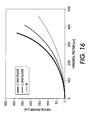
- FIGURE 16 shows the bending curves for the MoCr (stressed metal)/TiNi (SMA) cantilever actuator with 1.75 ⁇ m thick TiNi SMA film.
- the "LT, only elastic” means that the bending curve is calculated by using the mechanical property data of TiNi at cold or low temperature state and assuming only elastic deformation in the TiNi film.
- the "LT, only plastic” means that the bending curve is calculated by using the mechanical property data of TiNi at cold or low temperature state and assuming only plastic deformation in the TiNi film (will be explained later).
- the "HT” means that the bending curve is calculated by using the mechanical property data of TiNi at heated or high temperature state and assuming only elastic deformation in the TiNi film. It can be seen that the bending curves are significantly different between the cold state and heated state, thus can be used as actuators.
- the vertical position difference of the tip point or distal end between the cold state and heated state is the (net) tip displacement of the actuator.
- the dependence of displacement on the TiNi film thickness is given in FIGURE 17.
- the "only elastic deformation considered” means that when calculating the bending curve at cold state, the assumption is that there is only elastic deformation in the TiNi SMA film.
- the difference of bending curves between the cold state and heated state, or the tip displacement is only due to the difference of the Young's modulus between the martensite phase (cold state) and the austenite phase (heated state).
- the yield strength of the martensite phase is so low, it is possible that the stress induced in the TiNi film can be larger than the yield strength, thus plastic deformation can also be generated, which leads to more deformation in the structure. Therefore, when the bending curves are calculated, the average stress in the TiNi film is also calculated.
- Table 3 The results are tabulated in the following Table 3.
- the yield strength of TiNi martensite phase (low temperature or cold state) is 70 - 150MPa.
- the middle value, 110MPa is used for further calculation.
- the yield strength of the TiNi austenite phase (high temperature or heated state) is 690MPa. From Table 3 it can be seen that the average stress in the austenite phase is always far below the yield strength. This means that in under heated conditions, there is only elastic deformation in the TiNi layer. As such, under a heated condition, the bending curve is always calculated assuming only elastic deformation in the film. On the other hand, under cold conditions the average stress is already greater than the yield strength when the TiNi layer thickness is between 0.25 to 2.0 ⁇ m, thus plastic deformation should be considered.
- the calculated displacement gives the low limitation when only elastic deformation is considered and gives the high limitation when only plastic deformation is considered.
- the real displacement will be between these two limitations.
- the real displacement is the average of low and high limitations, from FIGURE 17 it can be observed that the optimized thickness for TiNi film is around 1.75 ⁇ m, which produces a tip displacement of about 103 ⁇ m.
- the thermal mismatch between the TiNi film and the MoCr film has not been taken into consideration. This is because the difference of thermal expansion coefficients between TiNi and MoCr is very small (6.0ppm/°C for TiNi and 5.265ppm/°C for MoCr). According to Timoshenko's bi-metal thermal actuator model (described in detail herein), the tip displacement generated by the thermal mismatch is just about 2 ⁇ m, which can be neglected.
- the spring constant or stiffness which describes how large a force can be generated by the actuator.
- the spring constant of a cantilever with multiple layers of different materials can be calculated based on principles of solid state mechanics and mechanics of materials known to those skilled in the art.
- the spring constant of the exemplary devices and the displacement results are given in Table 1. For these calculations, a device width of 100 ⁇ m was utilized.
- the tip displacement is calculated for a piezoelectric bimorph with a length of 500 ⁇ m and a total thickness of 3.75 ⁇ m.
- the device has two layers of piezoelectric PZT thin film with each thickness of 1.875 ⁇ m.
- L is the length
- t is the total thickness
- d 31 is the transverse piezoelectric constant
- E 3 is the applied field.
- Y is the Young's modulus
- l is the moment of inertia
- w is the width of the beam.
- a cantilever including a layer of silicon and a layer of aluminum is considered.
- This actuator has a much larger displacement than conventional bi-metal actuators with two metal layers because Si has a much smaller thermal expansion coefficient than metals and Al has a very high thermal expansion coefficient in metals.
- Si and Al have Young's moduli of 166GPa and 70GPa respectively, and thermal expansion coefficients of 2.8 and 23.1 ppm/°C, respectively.
- the cantilever thermal actuator has a length of 500 ⁇ m and total thickness of 3.75 ⁇ m, using the above two formulae one can calculate the tip displacement of the thermal actuator.
- the dependence of the tip displacement of a Si/Al thermal actuator on Si layer thickness is given in FIGURE 18.
- the optimized structure is around the Si layer thickness of 1.5 ⁇ m, or Al thickness of 2.25 ⁇ m, which gives the tip displacement of 60.3 ⁇ m.
- the spring constant can be calculated based on principles of solid state mechanics and mechanics of materials known to those skilled in the art, giving a value of 1.1 N/m.
- FIGURE 19 illustrates a device 1500 utilizing a stressed material layer such as stressed metal layer 1510 and a piezoelectric layer 1520, such as lead zirconate titanate, with one end secured to a substrate 1530.
- the piezoelectric layer 1520 is poled along the thickness direction.
- the stress or stress gradient in the stressed metal layer 1510 biases the device 1500 into a post-release, initial bending state, State A.
- an electric field with a direction parallel to the polarization direction of the piezoelectric layer 1520, it will cause the piezoelectric layer 1520 to expand in the thickness direction and contract in the length direction.
- State B When an electric field, with a direction parallel to the polarization direction of the piezoelectric layer 1520, it will cause the piezoelectric layer 1520 to expand in the thickness direction and contract in the length direction.
- State B When an electric field, with a direction parallel to the polarization direction of the piezoelectric layer 1520, it will cause the piezoelectric layer 1520 to
- a one layer structure which only utilizes the shape memory alloy material can be used.
- such a device 1600 only utilizes a single shape memory alloy layer 1610 with one end secured to a substrate 1620.
- a stress gradient exists in the shape memory alloy layer, as indicated by 1630, and this stress gradient will bias the structure into an initial bending state, State A.
- State A When changing the temperature and inducing the martensite-austenite phase transition in the shape memory alloy layer 1610, the structure will go to another bending State B. At low temperature the shape memory alloy layer 1610 is in martensite phase and is more ductile, and so the shape memory alloy layer 1610 bends more in State A than State B.
- a device can also comprise two or more layers of shape memory alloy materials with inherent stress or stress gradient in some or all of these layers.
- a device can have two shape memory alloy layers with one layer having inherent compressive stress and the other layer having inherent tensile stress. The stress or stress gradient will bias the device into an initial bending state. When changing the temperature and inducing the martensite-austenite phase transition in the shape memory alloy layer or layers, the device will go to another bending state. Thus, the device can be used as an actuator.
- the exemplary embodiment devices and systems described herein can utilize one or more components or sensors that enable precise control of the extent of bending of the assembly.
- the exemplary embodiment devices and systems can include an integrated sensor and/or an actuator that provides greater control and precision in the bending, deflection, or displacement of the device.
- an actuation circuit can be incorporated into the exemplary embodiment devices which utilize electrostatic actuation.
- a position sensing circuit can be incorporated that provides precise information as to the position or configuration of the device or structure.
- the exemplary embodiment can be applied in many industrial fields such as microactuators, micro-switches, microvalves and micropumps for microfluidic devices used in biological/biomedical area, many chemical analysis systems, optical shutters or shuttles, disk drive head actuation (for off-state slap protection), and arrays of cantilevers for printing and imaging.
- the exemplary embodiment devices can be readily fabricated.
Abstract
Description
- The present invention is generally related to MEMS devices and methods of manufacturing such devices. More particularly, the invention is related to a MEMS device comprising at least one shape memory material, such as a shape memory alloy layer and at least one stressed material layer. The device can be utilized as, for example, an actuator, a microswitch, a micropump, a microvalve, and a non-destructive fuse-type connection probe.
- Micro Electronic Mechanical Systems (MEMS) are microscopic devices and machines fabricated by integrating mechanical or hydraulic functions with electrical functions such as provided by computing/logic circuitry. MEMS technology has been widely utilized in a variety of industries. For example, a MEMS device can function as a sensing device, which combines a sensor and logic circuitry to perform monitoring functions such as pressure and acceleration measurement for deployment control of airbags in cars. A MEMS device can also function as a micromirror or waveguide to guide wavelengths in optical switches and tunable lasers. Typically, MEMS devices are processed with the same materials and methods used to make integrated circuits (IC's). Generally in producing a MEMS device, a tiny mechanical component such as a sensor, a valve, a gear, a mirror, and/or an actuator is incorporated in an electronic microchip such as a semiconductor chip.
- An actuator can be in the form of a MEMS device that, in responding to a signal received from a control system, can change and/or maintain the position of an element such as an end-effecter in performing a task. Shape memory alloys (SMA) have great potential as actuators due to their very high displacement and energy density. However, for most SMAs, the shape memory effect is a "one-time-only" actuation (one-way shape memory effect). That is, once a SMA is recovered to its original, un-deformed state by heating to above the martensite-austenite phase transition temperature, it will retain the un-deformed state and can not be automatically returned to its previous deformed state upon cooling.
- In accordance with one aspect of the present invention, a device comprises at least one layer of a shape memory material or materials; and
at least one layer of a stressed material or materials adjacent to the layer or layers of the shape memory material; the layer or layers of the stressed material possessing an inherent stress or stress gradient imparted to that layer or layers during its or their formation, such that as a result of the inherent stress or stress gradient in the layer or layers of the stressed material or materials, the device is biased to an initial deformation state. - Accordingly, the invention overcomes the noted problems, and provides an improved MEMS device by combining at least one shape memory alloy (SMA) layer and at least one stressed material layer, and incorporating the layered assembly in a MEMS device.
- Specifically, in one aspect of the exemplary embodiment, a device is provided which comprises a layer of a shape memory material, and a layer of a stressed material adjacent to the layer of the shape memory material. The layer of the stressed material possesses an inherent stress imparted to that layer during its formation. As a result of the inherent stress in the layer of the stressed material, the device is biased to an initial deformation state.
-
- FIGURE 1 shows a system in accordance with the exemplary embodiment having a cantilever structure with one layer of SMA film and one layer of a stressed metal film with deposited tensile stress or stress gradient.
- FIGURE 2 shows a system in accordance with the exemplary embodiment having a cantilever structure with one layer of SMA film, one layer of a first stressed metal film with deposited compressive stress, and one layer of another stressed metal film with deposited tensile stress.
- FIGURE 3 shows a system in accordance with the exemplary embodiment having a cantilever structure with one layer of a SMA film, one layer of a first stressed metal film, a second layer of a stressed metal film, and a layer of a piezoelectric material.
- FIGURE 4 shows a system in accordance with the exemplary embodiment having a diaphragm structure with one layer of SMA film, and one layer of a stressed metal film with deposited tensile stress.
- FIGURE 5 shows a system in accordance with the exemplary embodiment having a diaphragm structure with one layer of SMA film, one layer of a first stressed metal film with deposited compressive stress, and one layer of another stressed metal film with deposited tensile stress.
- FIGURE 6 shows a system in accordance with the exemplary embodiment having a diaphragm structure with one layer of SMA film, one layer of a first stressed metal film with deposited tensile stress, and one layer of another stressed metal film with deposited compressive stress.
- FIGURE 7 shows a system in accordance with the exemplary embodiment having a cantilever structure with a very thin dielectric layer deposited between the stressed metal film and the SMA film.
- FIGURE 8 is a detail of a distal free end of the structure shown in FIGURE 7.
- FIGURE 9 shows a top schematic view of a system in accordance with the exemplary embodiment having a cantilever structure with a narrow and long opening defined across a portion of the length of the assembly.
- FIGURE 10 illustrates the assembly of FIGURE 9 in a cold state and in a heated state.
- FIGURE 11 is an illustration of a stressed metal/SMA probe with a non-destructive fuse function.
- FIGURE 12 shows a system in accordance with the exemplary embodiment having a cantilever structure which combines thermal actuation and shape memory/stressed metal actuation.
- FIGURE 13 illustrates various steps in accordance with the exemplary embodiment to produce a stressed metal/SMA cantilever type micro device on a substrate.
- FIGURE 14 shows various steps in accordance with the exemplary embodiment to produce a stressed metal/SMA diaphragm type micro device on a substrate.
- FIGURE 15 illustrates various steps in accordance with the exemplary embodiment to produce a stressed metal/SMA diaphragm type micro device using a transfer method.
- FIGURE 16 is a bending curve for a MoCr (stressed metal)/TiNi (SMA) cantilever actuator.
- FIGURE 17 shows the relationship between tip displacement and TiNi film thickness in a cantilever type system in accordance with the exemplary embodiment.
- FIGURE 18 illustrates the relationship between tip displacement of a Si/Al thermal actuator and Si layer thickness in a system in accordance with the exemplary embodiment.
- FIGURE 19 shows a device in accordance with the exemplary embodiment having a cantilever structure with one layer of a stressed metal film and one layer of a piezoelectric material.
- FIGURE 20 shows a device in accordance with the exemplary embodiment having a cantilever structure with only one layer of SMA film which has an intrinsic stress gradient.
- The exemplary embodiment described herein relates to a multiple-layer device comprising one or more shape memory material layers such as shape memory alloy (SMA) layers and one or more stressed material layers such as stressed metal layers. In certain versions, the device utilizes a single layer configuration. The term "stressed material" as used herein refers to a material that includes an inherent or intrinsic mechanical stress or stress gradient. The inherent mechanical stress or stress gradient of the referenced stressed material is with respect to that material, or layer of that material, at its pre-release state during or after its manufacture. As described in greater detail herein, during formation of the devices and assemblies of the exemplary embodiment, one or more stresses are induced or otherwise created within the stressed material used in the device. At some phase in the manufacture of the device, the stressed material or layer of that material is physically released from an adjacent substrate or member. The release of that stressed material will alter the stresses and stress profile within that material. Thus, the stresses referred to in the definition of the term "stressed material" are those stresses existing prior to release of the material.
- A significant advantage of the exemplary embodiment is that unlike prior art layered assemblies using SMA's, a thermal mismatch between the stressed material layer and the shape memory layer(s) is not required. This thermal mismatch, relied upon by prior art assemblies, utilized the difference between coefficients of thermal expansion between the layer of shape memory material and another material which was typically a substrate.
- The stresses in the stressed material layer(s) can be either compressive or tensile. The stress can arise or be induced in the material in a variety of fashions. However, a typical strategy in producing a layer or film of a stressed material is to induce such stress during formation, such as by vapor deposition, of the material. If the stressed material is a stressed metal, either a tensile stress or a compressive stress, or a stress gradient can be imparted to a layer of the metal by appropriate selection of the deposition conditions. In one aspect of the exemplary embodiment, the stressed metal layer is formed by, in a controlled manner, depositing the material with compressive or tensile stress or a stress gradient in the layer. For example, when depositing a
MoCr 80/20 thin film, the intrinsic stress in the thin film changes as a function of Argon pressure, and the compressive-tensile stress can be controllably changed by more than -1.0 to + 1.0 GPa. The stressed material layer is generally deposited or otherwise disposed on the SMA layer. The SMA layer can be disposed on a MEMS substrate. The exemplary embodiment includes reversal of this order of layers, and also includes variations in the order of layers. The internal stress or stress gradient of the stressed metal material, when the SMA material is in its martensite phase, effectively causes the multiple-layer MEMS device to bend or otherwise be displaced away ortoward the MEMS substrate. Furthermore, as described in greater detail herein, one or more other materials besides metals may be used for the stressed material layer. - The exemplary embodiment can employ any suitable SMA material that undergoes a reversible crystalline phase transition, such as for example from martensite to austenite, when heated through its phase change transition temperature. Obtaining an intrinsic reversible effect for such a material can be accomplished by certain manufacturing methods for example by depositing the material by a method known as "Melt Spinning", or by the use of a thermo-mechanical treatment commonly referred to as the "education method" which induces a "memorized" preferred martensite shape to the SMA material. When the material is below its transition temperature, i.e., in its martensite phase, the material can be plastically deformed in response to an applied stress. During the phase transition, the material forcefully deforms toward the memory shape to which it is "trained" by, e.g., annealing.
- Merely by way of non-limiting examples, SMA materials which can be used in the exemplary embodiment include NiAI, TiNi, TiNiHf, TiNiCu, TiNiNb, TiNiPd, TiNiCo, TiPdNi, AgCd, AuCd, CuZn, CuZnGa, CuZnSi, CuZnSn, CuZnAl, CuAlNi, CuSn, CuAuZn, InTl, InCd, MnCd, and the like, and mixtures thereof.
- Suitable SMA materials for use in the exemplary embodiment, have an actuation energy density of from about 10 to about 200 MJ/m, and more specifically from about 80 to about 120 MJ/m3; and a recoverable strain of from about 0.1% to about 20%, and more specifically from about 5% to about 15%. However, it will be appreciated that the exemplary embodiment includes the use of SMA materials having different values for these characteristics.
- In another aspect of the exemplary embodiment, the SMA material is TiNi alloy, which is an alloy of nearly equal or different atomic weights of titanium and nickel. TiNi alloy not only has very useful thermo-mechanical properties such as a large energy density (1 J/g) and large displacement (10% strain), but it is also compatible with many biological agents. Sputtering is one way to fabricate a thin film of NiTi.
- The stressed materials suitable for use in the exemplary embodiment are any materials that provide or can be configured to provide sufficient mechanical stress bias to cause deformation of the selected SMA component in the MEMS device or system. And, as previously noted, these materials include a stress or stress gradient at the pre-release state of their manufacture. Exemplary stressed materials include, but are not limited to, metals, alloys, oxides, nitrides, semiconductors, Si, carbide, diamond, and various polymers etc. which have controllable internal stress or stress gradients. Representative stressed materials in the exemplary embodiment include, but are not limited to, metals and alloys such as Mo, "moly-chrome" alloy (MoCr), tungsten (W), titanium-tungsten alloy (TiW), chromium (Cr), nickel (Ni), and nickel-zirconium alloy (NiZr). In one aspect of the exemplary embodiment, the stressed material is a stressed metal alloy, such as MoCr.
- The stressed material layers used in the exemplary embodiment structures, devices, and systems described herein are also characterized by exhibiting a relatively homogenous or uniform composition. That is, the chemical composition of the stressed material layer generally does not vary, at least not to an appreciable extend, across the thickness of a layer of the material. The stressed material layers are deposited or prepared separately, and the composition or elements of the stressed material can be totally different from that of the SMA material. This is in contrast to metal films having stresses and a compositional gradient across their thickness, such as described in U.S. patents 6,689,486 and those described by Kuribayashi et al. in "Micron Sized Arm Using Reversible TiNi Alloy Thin Film Actuators," Mat. Res. Soc. Symp. Proc., Vol. 276, p. 167-176. (1992).
- Stressed metal films have been studied for use as contact probes for packaging and out-of-plane microcoils for RF electronics. For certain stressed materials, relatively large amounts of elastic or potential energy can be stored therein by bending or otherwise severely displacing the material, such as by bending the material in the form of a loop. These stressed materials are particularly useful for high energy or large displacement actuators in accordance with the exemplary embodiment described herein.
- Multi-layered devices and structures of the exemplary embodiment are also characterized by having, at least at the time immediately after their manufacture, a distinct boundary or interface between the layer of stressed material and an adjacent layer, such as a layer of a SMA. That is, for those devices or structures having at least one stressed material layer and at least one SMA layer, the region immediately between those layers is characterized by a distinct change in composition (due to compositional differences between the adjacent layers) and a distinct change in physical properties (likely due to the compositional difference). Furthermore, this region may also be characterized by a distinct difference in the types, profiles or gradients, or magnitudes of stress in the corresponding adjacent layers. Although the exemplary embodiment is primarily directed to layered arrays in which the stressed material layer is immediately adjacent to the SMA layer, other arrangements are contemplated. For example, these layers may be separated by one or more other layers, and so, not be immediately adjacent to one another.
- The MEMS device of the exemplary embodiment can take the structural form of a cantilever. With reference to FIGURE 1, a
system 100 having a cantilever configuration is constructed with one layer ofSMA film 110 and one layer of stressedmetal film 120 having a deposited tensile stress. Alternately, the stressedmetal film 120 can also have a stress gradient with a compressive stress near the bottom and a tensile stress at the top surface. Thesystem 100 can function as an actuator. TheSMA film 110 is affixed or otherwise secured to asubstrate 130. It will be appreciated that the tensile stress in themetal film 120 causes thefilm 120, and thus the collection oflayers metal film 120 to have a compressive stress, or a stress gradient with tensile stress near the bottom and compressive stress at the top surface. Alternately, the direction of curl could be reversed by reversing the arrangement of thelayers metal film 120 were located under theSMA film 110, an upward curl could be obtained by depositing the stressedmetal film 120 with a compressive stress. And, a downward curl could be obtained by depositing the stressed metal film (underneath the SMA film 110) to have a tensile stress. When thesystem 100 is in a cold state, i.e. the temperature is less than the phase change temperature of the SMA material, the cantilever structure will assume a position designated as "A" as shown in FIGURE 1. Upon heating thesystem 100 to a temperature greater than the phase change temperature of the SMA material, the structure will be displaced to a position designated as "B" in FIGURE 1. As previously explained, the displacement of the structure from position A to B, is caused by the increase in the modulus and/or yield strength of theSMA film 110 due to heating, which exceeds the mechanical bias imparted to the structure by the stressedmetal film 120. - With reference to FIGURE 2, a
system 200 having a "sandwich" type cantilever structure is constructed with one layer ofSMA film 210, one layer of a first stressedmetal film 220 with deposited compressive stress, and one layer of a second stressedmetal film 230 with deposited tensile stress. The collection offilms SMA film 210, are affixed or otherwise secured to asubstrate 240. As previously described with regard to FIGURE 1, upon heating, the structure is displaced from position A shown in FIGURE 6A, to position B. - In FIGURE 1 and FIGURE 2, stressed metal film(s) and SMA film are combined together to form active micro devices. The stressed metal film(s) provide a mechanical bias to the SMA films. More specifically, at low temperature or cold state, preferably at room temperature, the SMA film is in its martensite phase and has a lower Young's modulus and yield strength, and hence imparts a softer load on the stressed metal film. The stress or stress gradient in the stressed metal film(s) cause the device or assembly of films to be displaced to a state with a relatively large bending deformation. For a cantilever structure, this may be exhibited by the curvature of the displaced structure being smaller or "tighter." By raising the environmental temperature, or by applying heat, such as applying an electrical current flow through the device, the SMA film will transfer to its austenite phase and the device will exhibit much less deformation due to the large Young's modulus and high yield strength of the austenite phase. Preferably, the device will ideally recover to the un-deformed and flat state. This process can be reversed when the temperature is again lowered, and the device again is in the cold state and returns to the original, large bending or deformation state. The cycle can thus be repeated for many times as desired by repeatedly increasing and decreasing the temperature, which enables the exemplary embodiment MEMS device to function as a two-way, multiple-time actuation device.
- As previously illustrated in FIGURE 2, a collection of stressed material layers can be utilized instead of a single layer of a stressed material. In the case of stressed metals, it may be advantageous to use two or more layers in order to achieve a predetermined desired total stress for the layered system. By appropriately selecting particular types of stress, i.e. compressive or tensile, and their value or magnitude, a total stress can be calculated by summing the individual stresses to obtain a total stress. As an example, a desired total tensile stress can be obtained by the use of two layers of a stressed material so long as either (i) both stressed material layers each have a tensile stress which sums to the desired total, or (ii) if one has a compressive stress, then the other must have a tensile stress greater than the magnitude of the compressive stress of the other, and, the respective stresses must sum to the desired total.
- In addition to the SMA film and stressed material film, another functional material film can be deposited or otherwise incorporated in the layered array. For example, a film can be deposited which is used to more precisely to detect the position or shape of the device. This sensor film can have the same dimensions, or in certain embodiments, be smaller than the SMA film and stressed material film. For example, as depicted in FIGURE 3, a
smaller sensor film 250 is deposited on the device of FIGURE 2, and connected to an external electrical circuit throughwire connections sensor film 250 can be a piezoelectric thin film or a semiconductive piezoresistive material. When a piezoelectric thin film is used, under different curvature or device positions, the piezoelectric thin film will be under different stress conditions. Thus, the curvature or position of the device can be more accurately detected and controlled. - The MEMS device of the exemplary embodiment can also take the structural form of a diaphragm. FIGURE 4 shows a MEMS device or
system 300 with a diaphragm structure, which comprises one layer of aSMA film 310, one layer of a stressedmetal film 320 with deposited tensile stress, which is deposited or otherwise secured tosubstrates 330 that define a void or open space or region between them. In its cold state, the films are in position A. And, upon heating, the films are displaced to position B. This movement or displacement, as will be appreciated, can be utilized in a wide variety of applications such as the transfer of a fluid or liquid. - With reference to FIGURE 5, a diaphragm device or
system 400 is illustrated with one layer ofSMA film 410, one layer of a first stressedmetal film 420 with deposited compressive stress, and one layer of a second stressedmetal film 430 with deposited tensile stress. The collection offilms substrates 440. Upon heating the collection of films, the assembly is displaced from position A to position B. - FIGURE 6 illustrates a device or
system 500 having a diaphragm structure according to the exemplary embodiment with one layer ofSMA film 510, one layer of a first stressedmetal film 520 with deposited tensile stress, and one layer of a second stressedmetal film 530 with deposited compressive stress. The collection offilms substrates 540 that are spaced apart so as to provide an open region or space generally adjacent to one side of the collection of films. As previously described, the films are displaced from position A to position B by heating the films, and specifically, by heating theSMA film 510 to a temperature sufficient to induce a phase change. - In accordance with the exemplary embodiment, temperature control is crucial in triggering the SMA martensite-austenite phase transition. The characteristic temperatures of the beginning and end of the martensite-austenite transition are respectively designated As and Af. The characteristic temperatures of the beginning and end of the austenite-martensite transition are respectively designated Ms and Mf. For a specific SMA material, when the martensite-austenite transition is to be activated, the temperature should be higher than As, and preferably higher than Af. In contrast, when the austenite-martensite transition is to be activated, the temperature should be lower than Ms, and preferably lower than Mf.
- Depending upon the composition of the various layers, variations of the structure and combination of layers, and the structure of the MEMS device, the SMA phase transition temperature can be varied from about -200°C to about 110°C. Experiments on stressed metal springs indicate that cycling the spring between room temperature and 150°C will not substantially release the stress or stress gradient in the film. The transition temperature of most SMA films is about 60 to 75°C, or lower. Such thermal cycling should not cause stress degradation in the stressed metal film, hence the stressed metal/SMA actuators of the exemplary embodiment are reliable devices. Usually, the SMA thin films utilized in the exemplary embodiment devices are tuned to have the phase transition temperature greater than room temperature, i.e. 20°C, such as for example about 60 to about 75°C.
- The temperature control of the MEMS devices in accordance with the exemplary embodiment can be achieved by, in addition to adjusting the environmental temperature of the device, Joule or resistive heating such as applying an electrical current flow through the device, at up to several hundred Hz. By applying heating to induce the martensite-austenite phase transition, the device will exhibit much less bending deformation due to the high Young's modulus and yield strength of the austenite phase. By removing the applied current flow, the device will cool and return to its original, large bending or deformation state. The electrical current can be reapplied to the device and the cycle can be repeated as many times as desired.
- In one aspect of the exemplary embodiment, when electrical current flow is used to provide heating to the MEMS device with a cantilever structure, careful design is required so that current flows through the films so as to effectively generate heat. Generally, a wire connection is made at the fixed or clamped end of the layers. By way of examples, FIGURES 7, 8, 9 and 10 depict two cantilever-type actuation devices in which electric current is used to generate heating in a layered assembly. FIGURES 7 and 8 illustrate a
system 600 having alayer 610 of a SMA, and a layer of a stressedmetal 630, with a cantilever structure. Disposed between thelayers dielectric layer 620 such as silicon oxide. The device has a stack electrode configuration which can have electrical bias. As can be seen in FIGURE 7, one end of the layered assembly is affixed or otherwise secured to asubstrate 640. Specifically, the configuration of the distal orfree end 615 of the layered assembly is shown in FIGURE 8. There, it can be seen that thedielectric layer 620 does not completely extend to thedistal end 615 of the assembly. Instead, theSMA layer 610 and the stressedmetal layer 630 contact one another at only theend 615 and thereby provide electrical communication between thelayers wire connections layers connections layers end 615 detailed in FIGURE 8. - The exemplary embodiment also includes the use of an additional heating element, in addition to the layers of stressed material and the SMA. In this aspect, the separate heating element is incorporated in the layered array and provides heat to the layer of SMA. Such separate heating elements can generate heat in a variety of fashions, for example by resistance heating. In the event a separate heating element is not used, either or both of the layers of stressed material and SMA can serve as heating elements.
- FIGURES 9 and 10 illustrate a
cantilevered system 700 having an SMA Iayer710 and a stressed metal layer 720 defining a narrow andlong opening 730. It will be appreciated that thisopen region 730 could be filled with a dielectric material. FIGURE 10 is a perspective view showing the device in a cold state A, and a heated state B. Thedevice 700 has a coplanar electrode configuration which utilizes an electrical bias. Specifically, FIGURE 9 illustrates layers 710 and 720 attached at one end to asubstrate 740.Wire connections opening 730. Thus, upon connection to an electrical power source, current flows from one of theconnections - The exemplary embodiment also provides a multiple-layer non-destructive fuse-type connection probe, which can be used in, for example, packaging applications. The probe comprises one or more SMA layers and one or more stressed material layers such as stressed metal layers. In one aspect of the exemplary embodiment, the stressed metal layer is formed by, in a controlled manner, depositing the material with compressive or tensile stress or a stress gradient on the SMA layer. The internal stress or stress gradient of the stressed metal can, when the SMA material is in its martensite phase, effectively cause the multiple-layer probe to bend away or toward a connection point. An example of the stressed metal/SMA probe with a non-destructive fuse function is illustrated in FIGURE 11. With reference to FIGURE 11, a
system 800 is illustrated comprising aprobe 850 that is in selectable contact or communication with adevice 880. Theprobe 850 comprises aSMA layer 810 and a stressedmetal layer 820, which are secured or otherwise attached to asubstrate 830. Thedevice 880 includes a contact pad orsurface 870 defined or disposed on a substrate 860. The SMA film phase transition temperature can be so tuned to such an extent that, if the environmental temperature is greater than the safety temperature, the SMA film will transition to the austenite phase so that the probe will be disconnected from the device and move to position B. This is because the stressed metal is deformed relatively much less when the SMA transfers to the austenite phase. When the environmental temperature is lower, the probe will be connected to the device again, as in position A, as the SMA film will transfer back to the martensite phase. In another related aspect of this embodiment, the SMA film can be heated by passing a current through it (Joule heating). For a specific probe, a well-defined quantitative relationship between the electrical current through the probe and the temperature of the probe can be established. A safety current can therefore be calculated for a safety temperature, and vise versa. When the current in the probe is larger than the safety current, the SMA film will transfer to the austenite phase so that the probe will be disconnected from the device. Again when the current is lower, the probe will be connected to the device as the SMA film will transfer back to the martensite phase. In certain industrial fields, such probes can serve as non-destructive fuses, which will be automatically disconnected from the device if the environmental temperature or the current passing through the device is too high. - In another aspect of the exemplary embodiment, thermal actuation is coupled with a multiple-layer MEMS device. The device comprises one or more SMA layers, one or more stressed material layers such as stressed metal layers, and one or more layers of metal or other materials which have a sufficiently different thermal expansion coefficient as compared to those of the SMA and the stressed metal. An example of such a system is shown in FIGURE 12. Specifically,
system 900 comprises aSMA layer 910, a stressedmetal layer 930, a thin,dielectric layer 920 disposed between thelayers additional metal layer 940. The assembly oflayers substrate 950.Wire connections layers dielectric layer 920, is similar as the configuration depicted in FIGURE 8. As compared to the structure of FIGURES 9 and 10, theadditional metal layer 940 is deposited on top of the stressedmetal film 930. This additional metal layer has a much larger thermal expansion coefficient than MoCr and TiNi, such as Al. When the device is in a heated state, shown as "B", not only does the shape memory effect of the TiNi film cause the device to bend less, but also the thermal mismatch between the Al and MoCr/TiNi causes the device to bend less. Hence the device becomes more flat at a heated state, and extra displacement will be added to the displacement caused by the shape memory effect of the TiNi film. The cooled state is shown as "A." - In another aspect of the exemplary embodiment, thermal actuation is combined with stressed metal/SMA actuation in a different manner. In view of FIGURES 7, 8 and 12 it is contemplated to deposit on the SMA layer, a metal film that functions both as a stressed metal and as a metal with a much larger thermal expansion coefficient than the SMA film. Thus, the
extra metal layer 940 as shown in FIGURE 12 can be omitted in this strategy. That is, the MEMS actuator would have a similar structure as that shown in FIGURES 7 and 8, but would exhibit a performance similar to that shown in FIGURE 12. At a heated or high temperature condition, the device would be in a state with much less shape deformation due to both the phase transition of the SMA film and the thermal mismatch between the stressed metal film and the SMA film. - Additionally, the various devices and layered assemblies described herein can utilize layers of SMA and layers of stressed materials having a wide range of thicknesses. Generally, although the thicknesses of each layer depend upon a variety of factors, representative thicknesses for the SMA layer(s) range from about 0.1 µm to about 500 µm, typically from about 0.5 µm to about 10 µm, more typically from about 0.7 µm to about 4 µm, and in certain instances, from about 0.8 µm to about 2.5 µm. Similarly, representative thicknesses for the stressed material layer(s) range from about 0.1 µm to about 500 µm, typically from about 0.5 µm to about 10 µm , more typically from about 0.7 µm to about 4 µm, and in certain instances, from about 0.8 µm to about 2.5 µm. It will be understood that the exemplary embodiment described herein includes layer thicknesses greater than or less than these thicknesses.
- Although a wide array of stress magnitudes and stress types can be utilized in the layered assemblies and devices described herein, in certain embodiments, the stress in the stressed material is generally greater than 100 MPa. Similarly, a wide range of stress gradients can be utilized in the assemblies and devices described herein. In certain embodiments, the stress gradient in the stressed material is greater than 100 MPa/µm. As previously noted, these stress values are with respect to the stressed material at its pre-release state.
- The exemplary embodiment also provides methods of preparing the multiple-layer MEMS devices, which comprise one or more SMA layers and one or more stressed material layers such as stressed metal layers. In one aspect of the exemplary embodiment, the stressed metal layer is formed by, in a controlled manner, depositing the metal with compressive or tensile stress or a certain stress gradient on the SMA layer. The internal stress or stress gradient of the stressed metal can, when the SMA material is in its martensite phase, effectively cause the multiple-layer MEMS device to bend or otherwise be displaced away or toward the MEMS substrate. Since many SMA films need to be annealed at a temperature within a range of about 400 °C to 700°C after deposition, and many stressed metal films are usually deposited below 200°C, the method of the exemplary embodiment typically comprises depositing the SMA films first, and then depositing the stressed metal films. However, the exemplary embodiment methods include reversal of this sequence, as under some conditions SMA films can also be deposited below 200°C. The devices can be made on many substrates including, but not limited to, silicon, quartz, glass, and metal. Thus, a stable micro actuation device with very large displacement/force and simple structure can be easily developed.
- According to the exemplary embodiment, fabrication of a MEMS device having a cantilever structure can comprise the steps of (a) depositing a sacrificial layer on the substrate; (b) depositing and annealing a SMA film on the sacrificial layer; (c) depositing a stressed material film on the SMA film, in which the deposition parameters are controlled to induce stress or produce a particular stress gradient in the film; and (d) removing the sacrificial layer.
- In an aspect of the method according to the exemplary embodiment, a process is provided to form cantilever type devices on a silicon substrate. With reference to FIGURE 13, an
exemplary process 1000 comprises providing asubstrate 1010 such as a bare silicon wafer. Next, theprocess 1000 comprises depositing asacrificial layer 1020 such as amorphous silicon or PSG (phosphate glass). Then a portion of this sacrificial layer is removed by using a patterning method, such as a dry or wet chemical etching method. This is depicted in step (a) of FIGURE 13. Next, theprocess 1000 comprises depositing for example by evaporation, vapor deposition, or sputtering methods, aSMA film 1030, such as TiNi film, and annealing at 400 to 700°C for crystallization. A low temperature annealing process with an annealing temperature around or below 200°C can also be used. The process then includes depositing adielectric layer 1040 such as oxide or nitride, and patterning the dielectric layer. At this stage of the process, the assembly generally corresponds to that shown in (b) of FIGURE 13. Next, theprocess 1000 comprises depositing a stressedmetal film 1050, such as Ni or MoCr, in which the deposition parameters are controlled to induce stress or produce a desired stress gradient in the film, e.g., to have compressive stress at the bottom and tensile stress at the top. Then the stressedmetal film 1050 and theSMA film 1030 are patterned to remove a portion of each. The resulting assembly is shown in step (c) of FIGURE 13. Next, theprocess 1000 comprises a step of removing thesacrificial layer 1020 andbonding wire connections - According to the exemplary embodiment, fabrication of a MEMS device having a diaphragm structure can comprise the steps of (a) depositing a SMA film; (b) depositing a stressed material or stressed metal film, and controlling the deposition parameters to induce stress or produce a certain stress gradient in the film; and (c) removing part of the substrate to form a cavity.
- In a specific aspect of the exemplary embodiment, a method is provided to form diaphragm type devices on a substrate such as silicon. With reference to FIGURE 14, an
exemplary process 1100 comprises providing asubstrate 1110 such as a wafer of bare silicon. The process also includes depositing aSMA film 1120, such as TiNi film, in which the deposition can be performed for example by using evaporation, vapor deposition or sputtering methods, and annealing for crystallization by either using a conventional annealing process with an annealing temperature from about 400°C to about 700°C or a low temperature annealing process with an annealing temperature around or below 200°C. The resulting assembly corresponds to that shown in step (a) of FIGURE 14. Next, theprocess 1100 comprises depositing a stressedmetal film 1130, such as Ni or MoCr, and controlling the deposition parameters to induce stress or a stress gradient in the films, e.g., to have compressive stress at the bottom and tensile stress at the top. At this stage, the assembly corresponds to that shown in step (b) of FIGURE 15. Theprocess 1100 further comprises a step of patterning the stressedmetal film 1130 andSMA film 1120, removing a portion of the substrate to form a cavity, andbonding wire connections - If the substrate cannot withstand the temperature used to anneal the SMA film, or the order of SMA film and stressed metal film should be reversed, a transfer or lift-off process can be used. With reference to FIGURE 15, an
exemplary process 1200 provides a transfer method to produce a SMA/stressed metal diaphragm structure. First,exemplary process 1200 comprises providing asubstrate 1210 such as a wafer of bare silicon and depositing asacrificial layer 1220, such as amorphous silicon or PSG on thesubstrate 1210. The resulting assembly corresponds to that shown in step (a) of FIGURE 15. Next, the process includes depositing aSMA film 1230, such as TiNi film, in which the deposition can be done by using evaporation, vapor deposition or sputtering methods, and annealing for crystallization. The process also includes depositing a stressedmetal film 1240, such as Ni or MoCr, and controlling the deposition parameters to induce stress or a stress gradient in the films, e.g., to have tensile stress at the bottom and compressive stress at the top. The SMA film and stressed metal film can be patterned to remove a portion of each. At this stage, the assembly corresponds to that shown in step (b) of FIGURE 15. Next, the stressedmetal film 1240 is bonded or otherwise affixed to afinal target substrate 1250, and abonding layer 1260 is formed or otherwise disposed between the stressedmetal film 1240 and thetarget substrate 1250. Various bonding methods, such as thin film metal eutectic bonding, can be used. The resulting assembly corresponds to that shown in step (c) of FIGURE 15. Finally, thesacrificial layer 1220 is etched away and the stressedmetal film 1240/SMA film 1230 can be separated from thesubstrate 1210. Then thefinal target substrate 1250 is patterned to form a cavity. Electrodes orconductors - It is noted periodically herein that one or more layers can be patterned. It will be appreciated by those skilled in the art, that this refers to optional steps in which refining or finishing aspects are imparted to or performed upon one or more of the layers. These operations are merely optional with regard to the exemplary embodiment methods described herein, and are largely dictated by the particular application of the device or system being fabricated.
- Moreover, the layered structures and devices described herein also include the use of selective placement of a relatively small region or layer having a small "footprint" on a larger region or layer. The layer having the smaller footprint can be the stressed material, the SMA, or another functional material; and the layer having the larger footprint can be the stressed material, the SMA, or another functional material. For example, the exemplary embodiment includes a layered array or membrane structure in which only one or more perimeter regions or corners of the array include layers of a stressed material and a SMA.
- Advantageously, the exemplary embodiment provides micro devices that can be used as actuators, especially microvalves and micropumps, due to their large deformation ability and high energy density. Without being limited to any particular theory, the actuation is believed to be a result of the change of mechanical properties of the SMA films at different temperatures and effect of a stressed material in close proximity. The devices according to the exemplary embodiment have much larger displacement and actuation force than many other actuators. Also the devices can have very simple mechanical structures, and therefore can be easily fabricated.
- Moreover, the devices of the exemplary embodiment with a cantilever structure can be used as a packaging probe with a non-destructive fuse function. These MEMS devices also have great potential in microfluidic, especially biological fluidic areas, because the materials used in forming these devices are compatible with many biological agents. Specifically, examples of such materials include, but are not limited to silicon and TiNi alloy.
- The exemplary embodiment constituted as described above will now be described in further detail by way of working examples.
- For purpose of illustrating the advantages of the stressed metal/SMA micro devices for actuation applications, representative actuator models were established utilizing a cantilever structure and compared to cantilever piezoelectric bimorph and thermal bi-metal actuators. Theoretical calculations were conducted to acquire parameters such as tip displacement and spring constant.
- An actuator was modeled having a length of 500µm, a thickness of 3.75µm, and a width of 100µm. The actuator included a 1.75µm-thick TiNi layer, a 1 µm thick MoCr layer with -1GPa deposited compressive stress, and a 1µm thick MoCr layer with +1GPa deposited tensile stress. Tip displacement (µm) and spring constant (N/m) of the actuator are calculated and tabulated in Table 1, below.
- An actuator also having a length of 500µm, a thickness of 3.75µm, and a width of 100µm was modeled. The structure of the actuator included of two PZT films, each of which was 1.875 µm thick. Tip displacement (µm) and spring constant (N/m) of the actuator are calculated and tabulated in Table 1.
- An actuator also having a length of 500µm, a thickness of 3.75µm, and a width of 100µm was modeled. The structure of the actuator included a 1.5 µm thick Si film and 2.25µm-thick Al film. Tip displacement (µm) and spring constant (N/m) of the actuator are calculated and tabulated in Table 1.
- An actuator having a length of 100µm, a thickness of 3.75µm, and a width of 20µm was modeled. The structure of the actuator included a 1.75µm thick TiNi, 1µm thick MoCr layer with -1 GPa deposited compressive stress, and 1µm-thick MoCr with +1 GPa deposited tensile stress. Tip displacement (µm) and spring constant (N/m) of the actuator are calculated and tabulated in Table 1.
- An actuator also having a length of 100µm, a thickness of 3.75µm, and a width of 20µm was modeled. The structure of the actuator included two PZT films, each of which was 1.875 µm thick. Tip displacement (µm) and spring constant (N/m) of the actuator are calculated and tabulated in Table 1.
- An actuator also having a length of 100µm, a thickness of 3.75µm, and a width of 20µm was modeled. The structure of the actuator included a 1.5 µm thick Si film and 2.25µm thick Al film. Tip displacement (µm) and spring constant (N/m) of the actuator are calculated and tabulated in Table 1.
- A comparison between the stressed metal/SMA actuators, the piezoelectric bimorph and thermal actuators is summarized in Table 1. Sensitivity on the length of the cantilever was also been studied, and the results are given when the cantilever is 100µm long.
Table 1. Comparison between the Actuators of Examples 1-6 Actuator Tip displacement (µm) Spring constant (N/m) Example 1 103 1.6 Example 2 30 0.65 Example 3 60.3 1.1 Example 4 6.35 40.0 Example 5 1.20 16.3 Example 6 2.42 27.0 - The theoretical calculations are based on an analytical model developed by David Fork (David Fork et al, Proc. SPIE, Vol. 4176, pp. 226-235), herein incorporated by reference. This model computes the bend radius and neutral point of a bent cantilever for an arbitrary number of initially flat layers of specified modulus, thickness, and internal stress.
- Example 1 cantilever structure is 500µm in length and includes three layers: a layer of TiNi SMA film with various thickness values, a layer of MoCr layer which is 1µm thick and having an initial, deposited stress of -1 GPa (compressive stress), and another layer of MoCr layer which is also 1µm thick but having an initial, deposited stress of +1 GPa (tensile stress). The mechanical properties of the MoCr layer and TiNi layer are given in Table 2. In the displacement calculation, bending modulus is used. Bending modulus = Y / (1 - ν2), wherein Y is the Young's modulus and ν is the Poisson's ratio.
Table 2. Mechanical properties of the MoCr and TiNi films Material Young's Modulus (GPa) Yield Strength (MPa) Poisson's Ratio Biaxial Modulus (GPa) Bending Modulus (GPa) MoCr 321.5 >2000 0.295 458.26 352.15 TiNi, heated 83 690 0.33 123.88 93.14 TiNi, cold 34 70-150 0.33 50.75 38.16 - FIGURE 16 shows the bending curves for the MoCr (stressed metal)/TiNi (SMA) cantilever actuator with 1.75µm thick TiNi SMA film. The "LT, only elastic" means that the bending curve is calculated by using the mechanical property data of TiNi at cold or low temperature state and assuming only elastic deformation in the TiNi film. The "LT, only plastic" means that the bending curve is calculated by using the mechanical property data of TiNi at cold or low temperature state and assuming only plastic deformation in the TiNi film (will be explained later). The "HT" means that the bending curve is calculated by using the mechanical property data of TiNi at heated or high temperature state and assuming only elastic deformation in the TiNi film. It can be seen that the bending curves are significantly different between the cold state and heated state, thus can be used as actuators.
- By definition, the vertical position difference of the tip point or distal end between the cold state and heated state is the (net) tip displacement of the actuator. The dependence of displacement on the TiNi film thickness is given in FIGURE 17.
- In FIGURE 17, the "only elastic deformation considered" means that when calculating the bending curve at cold state, the assumption is that there is only elastic deformation in the TiNi SMA film. Thus the difference of bending curves between the cold state and heated state, or the tip displacement, is only due to the difference of the Young's modulus between the martensite phase (cold state) and the austenite phase (heated state). However, as the yield strength of the martensite phase is so low, it is possible that the stress induced in the TiNi film can be larger than the yield strength, thus plastic deformation can also be generated, which leads to more deformation in the structure. Therefore, when the bending curves are calculated, the average stress in the TiNi film is also calculated. The results are tabulated in the following Table 3.
Table 3. Average Stresses in the TiNi SMA Film TiNi thickness (µm) Average axial strain in TiNi at LT Average axial stress in TiNi at LT (MPa) Average axial strain in TiNi at HT Average axial stress in TiNi at HT (MPa) 0.25 0.440% 149.43 0.405% 335.92 0.50 0.451% 153.30 0.379% 314.53 0.75 0.450% 152.93 0.344% 285.76 1.00 0.438% 148.87 0.306% 254.26 1.25 0.418% 141.98 0.269% 223.32 1.50 0.392% 133.23 0.235% 194.81 1.75 0.363% 123.48 0.204% 169.53 2.00 0.334% 113.43 0.178% 147.60 2.25 0.305% 103.59 0.155% 128.82 2.50 0.277% 94.26 0.136% 112.82 2.75 0.252% 85.61 0.120% 99.22 3.00 0.229% 77.72 0.106% 87.64 3.25 0.208% 70.59 0.094% 77.77 3.50 0.189% 64.19 0.084% 69.32 - The yield strength of TiNi martensite phase (low temperature or cold state) is 70 - 150MPa. The middle value, 110MPa, is used for further calculation. The yield strength of the TiNi austenite phase (high temperature or heated state) is 690MPa. From Table 3 it can be seen that the average stress in the austenite phase is always far below the yield strength. This means that in under heated conditions, there is only elastic deformation in the TiNi layer. As such, under a heated condition, the bending curve is always calculated assuming only elastic deformation in the film. On the other hand, under cold conditions the average stress is already greater than the yield strength when the TiNi layer thickness is between 0.25 to 2.0µm, thus plastic deformation should be considered.
- Calculating the bending curve by combining both elastic deformation and plastic deformation is relatively complicated such that only an extreme condition is considered in this analysis, that is, there is only plastic deformation in the TiNi film. This means that the TiNi film has zero Young's modulus but has a stress of 110MPa which resists the bending. The bending curve and the displacement under this assumption are calculated, and the results are shown in FIGURE 17, corresponding to the curve of "Only plastic deformation considered".
- The calculated displacement gives the low limitation when only elastic deformation is considered and gives the high limitation when only plastic deformation is considered. The real displacement will be between these two limitations. By reasonably assuming that the real displacement is the average of low and high limitations, from FIGURE 17 it can be observed that the optimized thickness for TiNi film is around 1.75µm, which produces a tip displacement of about 103µm.
- In the above calculations, the thermal mismatch between the TiNi film and the MoCr film has not been taken into consideration. This is because the difference of thermal expansion coefficients between TiNi and MoCr is very small (6.0ppm/°C for TiNi and 5.265ppm/°C for MoCr). According to Timoshenko's bi-metal thermal actuator model (described in detail herein), the tip displacement generated by the thermal mismatch is just about 2µm, which can be neglected.
- In addition to the displacement, another important parameter for actuators is the spring constant or stiffness, which describes how large a force can be generated by the actuator. By assuming the materials have isotropic properties and identical width and length for each layer, and the force is applied on the tip position, the spring constant of a cantilever with multiple layers of different materials can be calculated based on principles of solid state mechanics and mechanics of materials known to those skilled in the art. The spring constant of the exemplary devices and the displacement results are given in Table 1. For these calculations, a device width of 100µm was utilized.
- Comparative calculations on piezoelectric and thermal actuators which are also cantilever structures, can be extended to diaphragm structures.
- First, the tip displacement is calculated for a piezoelectric bimorph with a length of 500µm and a total thickness of 3.75µm. The device has two layers of piezoelectric PZT thin film with each thickness of 1.875µm. The tip displacement of a piezoelectric bimorph is given as:

- In the above equation, L is the length, t is the total thickness, d 31 is the transverse piezoelectric constant, and E 3 is the applied field.
- Because the mechanical properties of the two layers in this piezoelectric cantilever are the same, they can be considered as one layer in calculating the spring constant. The spring constant for a single beam can be written as:

- In the above equation, Y is the Young's modulus, l is the moment of inertia, and w is the width of the beam.
- Based on these two formulae and the properties of PZT ceramic thin films, the tip displacement and spring constant of a piezoelectric bimorph actuator have also been calculated. The results are listed in Table 4.
Table 4. Tip displacement and spring constant of a piezoelectric bimorph Beam material PZT Young's Modulus (GPa) 62 d31 (pm/V) -100 Applied field (V/µm) 3 Tip displacement (µm) 30 Spring constant (N/m) 0.65 - For a bi-metal thermal actuator, a cantilever including a layer of silicon and a layer of aluminum is considered. This actuator has a much larger displacement than conventional bi-metal actuators with two metal layers because Si has a much smaller thermal expansion coefficient than metals and Al has a very high thermal expansion coefficient in metals.
- The bending curvature of a bi-metal strip is given by Timoshenko, (S. Timoshenko, J. Opt. Soc. Am., Vol. 11, p. 233, 1925), herein incorporated by reference, and can be written as:

- For the cantilever structure where one end is mechanically fixed, the tip displacement of the other end can be calculated as:

where L is length of the cantilever. - Si and Al have Young's moduli of 166GPa and 70GPa respectively, and thermal expansion coefficients of 2.8 and 23.1 ppm/°C, respectively. As the TiNi SMA films for MEMS actuators usually have the phase transition temperatures between 60 to 75°C, one can assume that the temperature change for the thermal actuators is from room temperature (20°C) to 80°C, thus ΔT = 60°C. When the cantilever thermal actuator has a length of 500µm and total thickness of 3.75µm, using the above two formulae one can calculate the tip displacement of the thermal actuator. The dependence of the tip displacement of a Si/Al thermal actuator on Si layer thickness is given in FIGURE 18.
- From FIGURE 18, it can be seen that the optimized structure is around the Si layer thickness of 1.5µm, or Al thickness of 2.25µm, which gives the tip displacement of 60.3µm. Assuming the width is 100µm, the spring constant can be calculated based on principles of solid state mechanics and mechanics of materials known to those skilled in the art, giving a value of 1.1 N/m.
- For example, FIGURE 19 illustrates a
device 1500 utilizing a stressed material layer such as stressedmetal layer 1510 and apiezoelectric layer 1520, such as lead zirconate titanate, with one end secured to asubstrate 1530. Thepiezoelectric layer 1520 is poled along the thickness direction. The stress or stress gradient in the stressedmetal layer 1510 biases thedevice 1500 into a post-release, initial bending state, State A. When an electric field, with a direction parallel to the polarization direction of thepiezoelectric layer 1520, is applied to thepiezoelectric layer 1520, it will cause thepiezoelectric layer 1520 to expand in the thickness direction and contract in the length direction. Thus thedevice 1500 will become less bent and change to State B. On the other hand, when an electric field, with a direction anti-parallel to the polarization direction of thepiezoelectric layer 1520, is applied to thepiezoelectric layer 1520, it will cause thepiezoelectric layer 1520 to contract in the thickness direction and expand in the length direction. Thus thedevice 1500 will become more bent and change to State C. When an AC electric field is applied to thepiezoelectric layer 1520, thedevice 1500 will change between State B and State C. - Moreover, in addition to the stressed metal/shape memory alloy two layer structure, a one layer structure which only utilizes the shape memory alloy material can be used. As shown in FIGURE 20, such a
device 1600 only utilizes a single shapememory alloy layer 1610 with one end secured to asubstrate 1620. A stress gradient exists in the shape memory alloy layer, as indicated by 1630, and this stress gradient will bias the structure into an initial bending state, State A. When changing the temperature and inducing the martensite-austenite phase transition in the shapememory alloy layer 1610, the structure will go to another bending State B. At low temperature the shapememory alloy layer 1610 is in martensite phase and is more ductile, and so the shapememory alloy layer 1610 bends more in State A than State B. Similarly, a device can also comprise two or more layers of shape memory alloy materials with inherent stress or stress gradient in some or all of these layers. For example, a device can have two shape memory alloy layers with one layer having inherent compressive stress and the other layer having inherent tensile stress. The stress or stress gradient will bias the device into an initial bending state. When changing the temperature and inducing the martensite-austenite phase transition in the shape memory alloy layer or layers, the device will go to another bending state. Thus, the device can be used as an actuator. - Furthermore, the exemplary embodiment devices and systems described herein can utilize one or more components or sensors that enable precise control of the extent of bending of the assembly. Specifically, the exemplary embodiment devices and systems can include an integrated sensor and/or an actuator that provides greater control and precision in the bending, deflection, or displacement of the device. For example, an actuation circuit can be incorporated into the exemplary embodiment devices which utilize electrostatic actuation. In addition, a position sensing circuit can be incorporated that provides precise information as to the position or configuration of the device or structure. These and other aspects are described in U.S. patent 6,734,425, herein incorporated by reference.
- It will be understood that although many of the references to the exemplary embodiment refer to a single structure or MEMS device, in practice, a collection or array of structures or devices will be utilized. For example, it is clearly within the scope of the exemplary embodiment to utilize an array of cantilevers, or an array of membranes. In many MEMS applications, artisans use multiple devices or arrays of devices or structures rather than a single device.
- The exemplary embodiment can be applied in many industrial fields such as microactuators, micro-switches, microvalves and micropumps for microfluidic devices used in biological/biomedical area, many chemical analysis systems, optical shutters or shuttles, disk drive head actuation (for off-state slap protection), and arrays of cantilevers for printing and imaging. The exemplary embodiment devices can be readily fabricated.
Claims (18)
- A device comprising:at least one layer of a shape memory material or materials (110, 210, 310, 410, 510, 610, 710, 810, 910, 1030, 1120, 1230); andat least one layer of a stressed material or materials (120, 220, 320, 420, 520, 620, 720, 820, 920, 1050, 1130, 1240) adjacent to the layer or layers of the shape memory material; the layer or layers of the stressed material possessing an inherent stress or stress gradient imparted to that layer or layers during its or their formation, such that as a result of the inherent stress or stress gradient in the layer or layers of the stressed material or materials, the device is biased to an initial deformation state.
- The device of claim 1, wherein the shape memory material is a shape memory alloy (SMA) selected from the group consisting of NiAl, TiNi, TiNiHf, TiNiCu, TiNiNb, TiNiPd, TiNiCo, TiPdNi, AgCd, AuCd, CuZn, CuZnGa, CuZnSi, CuZnSn, CuZnAl, CuAlNi, CuSn, CuAuZn, InTl, InCd, MnCd, and combinations thereof.
- The device of claim 1 or claim 2, wherein the shape memory material is selected from the group consisting of polymer materials, ceramic materials, and combinations thereof.
- The device of any of the preceding claims, wherein the stressed material is selected from the group consisting of metal, alloy, oxide, nitride, semiconductor, silicon (Si), carbide, diamond, ceramics, polymer, and combinations thereof.
- The device of claim 4, wherein the stressed material is a metal or alloy selected from the group consisting of Ni, Mo, "molybdenum-chrome" alloy (MoCr), tungsten (W), titanium-tungsten alloy (TiW), chromium (Cr), nickel (Ni), nickel-zirconium alloy (NiZr), and combinations thereof.
- The device of any of the preceding claims, wherein the shape memory material has a martensite-austenite phase transition temperature of from about -200°C to about 110°C.
- The device of any of the preceding claims further comprising electrical contacts (260, 270; 650, 660, 750, 760; 960; 970; 1060, 1070; 1140, 1150; 1270, 1280) for providing electrical communication to at least one of the layer of the shape memory material and the layer of the stressed material, whereby upon passing an electrical current through the electrical contacts and layer(s) in communication therewith, heat is generated.
- The device of any of the preceding claims, further comprising a resistive heating element.
- The device of any of the preceding claims, further comprising a thin film sensor layer (250) to detect the deformation of the device, the thin film layer having dimensions equal or smaller than corresponding dimensions of at least one of the shape memory layer and the stressed material layer, and the thin film layer including a material selected from the group consisting of a piezoelectric material, a piezoresistive material, and combinations thereof.
- The device of any of the preceding claims, wherein the device is selected from the group consisting of an actuator, a microswitch, a microvalve, a micropump, and a non-destructive fuse-type connection probe.
- A reversible and selectively deformable MEMS device comprising:a released assembly including (i) at least one layer of a stressed material having an inherent mechanical stress or stress gradient, the stress being defined at a pre-release state of the assembly, and (ii) at least one other layer proximate to the layer of stressed material, the other layer serving to apply a mechanical load upon the layer of stressed material;wherein the inherent mechanical stress in the layer of stressed material causes the assembly to assume a post-release state, and upon selectively changing the physical properties of the other layer, the assembly is reversibly and selectively deformed to another state different than the post-release state.
- The device of claim 11, wherein the other layer is one of a piezoelectric material having physical properties that can be changed by applying an electric field, an electrostrictive material having physical properties that can be changed by applying an electric field, and a magnetostrictive material having physical properties that can be changed by applying a magnetic field.
- A method of making a device including (i) at least one shape memory alloy (SMA) layer and (ii) at least one stressed material layer, the device having a cantilever structure, the method comprising:providing a substrate,depositing a sacrificial layer on the substrate;depositing and annealing a SMA film ;depositing a stressed material film, in which the deposition parameters of the stressed material are controlled to induce stress or produce a stress gradient in the stressed material film; andat least partially removing the sacrificial layer, to thereby release the SMA film and stressed material film from the substrate and produce a cantilevered layered device.
- A method of making a device including (i) at least one shape memory alloy (SMA) layer and (ii) at least one stressed material layer, the device having a diaphragm structure, the method comprising:providing a substrate;depositing a SMA film;depositing a stressed material film and controlling the deposition parameters to induce stress or stress gradient in the stressed material film; andpatterning the substrate material to form a cavity.
- The method of claim 13 or claim 14, in which the SMA film is deposited by a process selected from the group consisting of evaporation, vapor deposition, and sputtering methods.
- The method of any of claims 13 to 15, further including annealing the SMA film at a temperature within the range of from about 400°C to about 800°C.
- A method of producing a device including (i) at least one shape memory alloy (SMA) layer and (ii) at least one stressed material layer, the method comprising:providing a first substrate;depositing a sacrificial layer on the substrate;depositing and annealing a SMA film ;depositing a stressed material film , wherein the deposition parameters are controlled to induce stress or produce a stress gradient in the stressed material film;affixing a target substrate to the stressed material film; andremoving the sacrificial layer and the first substrate.
- A MEMS device according to any of claims 1 to 10.
Applications Claiming Priority (1)
| Application Number | Priority Date | Filing Date | Title |
|---|---|---|---|
| US10/923,277 US7372348B2 (en) | 2004-08-20 | 2004-08-20 | Stressed material and shape memory material MEMS devices and methods for manufacturing |
Publications (2)
| Publication Number | Publication Date |
|---|---|
| EP1630416A1 true EP1630416A1 (en) | 2006-03-01 |
| EP1630416B1 EP1630416B1 (en) | 2018-11-21 |
Family
ID=35385542
Family Applications (1)
| Application Number | Title | Priority Date | Filing Date |
|---|---|---|---|
| EP05254972.2A Expired - Fee Related EP1630416B1 (en) | 2004-08-20 | 2005-08-10 | Shape memory material device and method for manufacturing |
Country Status (3)
| Country | Link |
|---|---|
| US (2) | US7372348B2 (en) |
| EP (1) | EP1630416B1 (en) |
| JP (1) | JP5883203B2 (en) |
Cited By (11)
| Publication number | Priority date | Publication date | Assignee | Title |
|---|---|---|---|---|
| NL2000209C2 (en) * | 2006-09-04 | 2008-03-05 | Univ Delft Tech | Thermal actuator for e.g. microfluidic components, comprises alternating layers of two different materials |
| WO2009147135A1 (en) * | 2008-06-02 | 2009-12-10 | Leibniz-Institut Für Festkörper- Und Werkstoffforschung Dresden E.V. | Construction element made of a ferromagnetic shape memory material and use thereof |
| WO2012145278A3 (en) * | 2011-04-19 | 2013-08-15 | Eastman Kodak Company | Mems composite transducer including compliant membrane |
| TWI408001B (en) * | 2011-03-01 | 2013-09-11 | Univ Nat Taipei Technology | Microfluidic valve and mixer using shape memory material |
| US8631711B2 (en) | 2011-04-19 | 2014-01-21 | Eastman Kodak Company | MEMS composite transducer including compliant membrane |
| CN106918397A (en) * | 2015-12-28 | 2017-07-04 | 中芯国际集成电路制造(上海)有限公司 | MEMS, MEMS temperature sensor and respective preparation method |
| GB2602950A (en) * | 2017-05-05 | 2022-07-20 | Hutchinson Technology | Shape memory alloy actuators and methods thereof |
| US11668288B2 (en) | 2017-05-05 | 2023-06-06 | Hutchinson Technology Incorporated | Shape memory alloy actuators and methods thereof |
| US11686294B2 (en) | 2017-05-05 | 2023-06-27 | Hutchinson Technology Incorporated | Shape memory alloy actuators and methods thereof |
| US11815794B2 (en) | 2017-05-05 | 2023-11-14 | Hutchinson Technology Incorporated | Shape memory alloy actuators and methods thereof |
| US11859598B2 (en) | 2021-06-10 | 2024-01-02 | Hutchinson Technology Incorporated | Shape memory alloy actuators and methods thereof |
Families Citing this family (110)
| Publication number | Priority date | Publication date | Assignee | Title |
|---|---|---|---|---|
| US7655001B2 (en) * | 2001-03-23 | 2010-02-02 | Petrakis Dennis N | Temperature responsive systems |
| FR2868591B1 (en) * | 2004-04-06 | 2006-06-09 | Commissariat Energie Atomique | MICROCOMMUTER WITH LOW ACTUATION VOLTAGE AND LOW CONSUMPTION |
| US7944599B2 (en) | 2004-09-27 | 2011-05-17 | Qualcomm Mems Technologies, Inc. | Electromechanical device with optical function separated from mechanical and electrical function |
| US7304784B2 (en) * | 2004-09-27 | 2007-12-04 | Idc, Llc | Reflective display device having viewable display on both sides |
| US7420725B2 (en) * | 2004-09-27 | 2008-09-02 | Idc, Llc | Device having a conductive light absorbing mask and method for fabricating same |
| US7527995B2 (en) * | 2004-09-27 | 2009-05-05 | Qualcomm Mems Technologies, Inc. | Method of making prestructure for MEMS systems |
| US8008736B2 (en) * | 2004-09-27 | 2011-08-30 | Qualcomm Mems Technologies, Inc. | Analog interferometric modulator device |
| US7564612B2 (en) * | 2004-09-27 | 2009-07-21 | Idc, Llc | Photonic MEMS and structures |
| US7630119B2 (en) | 2004-09-27 | 2009-12-08 | Qualcomm Mems Technologies, Inc. | Apparatus and method for reducing slippage between structures in an interferometric modulator |
| US7289259B2 (en) | 2004-09-27 | 2007-10-30 | Idc, Llc | Conductive bus structure for interferometric modulator array |
| US7130104B2 (en) * | 2004-09-27 | 2006-10-31 | Idc, Llc | Methods and devices for inhibiting tilting of a mirror in an interferometric modulator |
| US7372613B2 (en) | 2004-09-27 | 2008-05-13 | Idc, Llc | Method and device for multistate interferometric light modulation |
| US7444812B2 (en) * | 2005-01-27 | 2008-11-04 | Scott Ryan Kirkpatirck | Shape memory alloy MEMS heat engine |
| US7321185B2 (en) * | 2005-03-04 | 2008-01-22 | United States Of America As Represented By The Administrator Of The National Aeronautics And Space Administration | Active multistable twisting device |
| US7916980B2 (en) | 2006-01-13 | 2011-03-29 | Qualcomm Mems Technologies, Inc. | Interconnect structure for MEMS device |
| US7550810B2 (en) * | 2006-02-23 | 2009-06-23 | Qualcomm Mems Technologies, Inc. | MEMS device having a layer movable at asymmetric rates |
| SG135993A1 (en) * | 2006-03-20 | 2007-10-29 | Sony Corp | Components having a film structure and methods of forming components having a film structure |
| US7649671B2 (en) * | 2006-06-01 | 2010-01-19 | Qualcomm Mems Technologies, Inc. | Analog interferometric modulator device with electrostatic actuation and release |
| US7527998B2 (en) * | 2006-06-30 | 2009-05-05 | Qualcomm Mems Technologies, Inc. | Method of manufacturing MEMS devices providing air gap control |
| US8190331B2 (en) * | 2006-11-01 | 2012-05-29 | GM Global Technology Operations LLC | Systems for detecting animate objects in a vehicle compartment |
| KR100834829B1 (en) * | 2006-12-19 | 2008-06-03 | 삼성전자주식회사 | Multi-bit electro-mechanical memory device and method manufacturing the same |
| US8115987B2 (en) * | 2007-02-01 | 2012-02-14 | Qualcomm Mems Technologies, Inc. | Modulating the intensity of light from an interferometric reflector |
| US7643202B2 (en) * | 2007-05-09 | 2010-01-05 | Qualcomm Mems Technologies, Inc. | Microelectromechanical system having a dielectric movable membrane and a mirror |
| US20080302024A1 (en) * | 2007-06-05 | 2008-12-11 | Gm Global Technology Operations, Inc. | Tunable impedance load-bearing structures |
| EP2168180A1 (en) * | 2007-06-15 | 2010-03-31 | Telezygology Inc. | Stacked morphing actuator |
| US7630121B2 (en) | 2007-07-02 | 2009-12-08 | Qualcomm Mems Technologies, Inc. | Electromechanical device with optical function separated from mechanical and electrical function |
| WO2009018287A1 (en) | 2007-07-31 | 2009-02-05 | Qualcomm Mems Technologies, Inc. | Devices for enhancing colour shift of interferometric modulators |
| US7936240B2 (en) * | 2007-08-16 | 2011-05-03 | Simon Fraser University | Lithographically controlled curvature for MEMS devices and antennas |
| US7773286B2 (en) * | 2007-09-14 | 2010-08-10 | Qualcomm Mems Technologies, Inc. | Periodic dimple array |
| EP2191320A2 (en) * | 2007-09-17 | 2010-06-02 | Qualcomm Mems Technologies, Inc. | Semi-transparent / transflective lighted interferometric modulator devices |
| US20090078316A1 (en) * | 2007-09-24 | 2009-03-26 | Qualcomm Incorporated | Interferometric photovoltaic cell |
| JP4924347B2 (en) * | 2007-10-03 | 2012-04-25 | コニカミノルタホールディングス株式会社 | Moving mechanism, imaging unit, and imaging apparatus |
| JP5209727B2 (en) * | 2007-10-19 | 2013-06-12 | クォルコム・メムズ・テクノロジーズ・インコーポレーテッド | Display with integrated photovoltaic device |
| US8058549B2 (en) * | 2007-10-19 | 2011-11-15 | Qualcomm Mems Technologies, Inc. | Photovoltaic devices with integrated color interferometric film stacks |
| CN101419379A (en) * | 2007-10-23 | 2009-04-29 | 鸿富锦精密工业(深圳)有限公司 | Camera module with automatic focusing function and focusing method thereof |
| US8054527B2 (en) * | 2007-10-23 | 2011-11-08 | Qualcomm Mems Technologies, Inc. | Adjustably transmissive MEMS-based devices |
| US20090293955A1 (en) * | 2007-11-07 | 2009-12-03 | Qualcomm Incorporated | Photovoltaics with interferometric masks |
| US8941631B2 (en) * | 2007-11-16 | 2015-01-27 | Qualcomm Mems Technologies, Inc. | Simultaneous light collection and illumination on an active display |
| KR100959454B1 (en) * | 2007-12-10 | 2010-05-25 | 주식회사 동부하이텍 | Semiconductor device and method for fabricating the same |
| KR20100109924A (en) * | 2007-12-21 | 2010-10-11 | 퀄컴 엠이엠스 테크놀로지스, 인크. | Multijunction photovoltaic cells |
| US8164821B2 (en) * | 2008-02-22 | 2012-04-24 | Qualcomm Mems Technologies, Inc. | Microelectromechanical device with thermal expansion balancing layer or stiffening layer |
| US7944604B2 (en) | 2008-03-07 | 2011-05-17 | Qualcomm Mems Technologies, Inc. | Interferometric modulator in transmission mode |
| US7612933B2 (en) * | 2008-03-27 | 2009-11-03 | Qualcomm Mems Technologies, Inc. | Microelectromechanical device with spacing layer |
| JP4941389B2 (en) * | 2008-04-08 | 2012-05-30 | コニカミノルタホールディングス株式会社 | Drive device |
| US8451077B2 (en) | 2008-04-22 | 2013-05-28 | International Business Machines Corporation | MEMS switches with reduced switching voltage and methods of manufacture |
| US8023167B2 (en) * | 2008-06-25 | 2011-09-20 | Qualcomm Mems Technologies, Inc. | Backlight displays |
| US8174352B2 (en) * | 2008-06-26 | 2012-05-08 | Cornell University | Method for making a transducer, transducer made therefrom, and applications thereof |
| US7859740B2 (en) * | 2008-07-11 | 2010-12-28 | Qualcomm Mems Technologies, Inc. | Stiction mitigation with integrated mech micro-cantilevers through vertical stress gradient control |
| US8358266B2 (en) * | 2008-09-02 | 2013-01-22 | Qualcomm Mems Technologies, Inc. | Light turning device with prismatic light turning features |
| US20100051089A1 (en) * | 2008-09-02 | 2010-03-04 | Qualcomm Mems Technologies, Inc. | Light collection device with prismatic light turning features |
| WO2010044901A1 (en) * | 2008-10-16 | 2010-04-22 | Qualcomm Mems Technologies, Inc. | Monolithic imod color enhanced photovoltaic cell |
| US8237324B2 (en) * | 2008-12-10 | 2012-08-07 | The Regents Of The University Of California | Bistable electroactive polymers |
| US20100189444A1 (en) * | 2009-01-27 | 2010-07-29 | General Electric Company | Optical mems device and remote sensing system utilizing the same |
| US8270056B2 (en) * | 2009-03-23 | 2012-09-18 | Qualcomm Mems Technologies, Inc. | Display device with openings between sub-pixels and method of making same |
| CN102342014B (en) * | 2009-04-17 | 2014-05-07 | 阿尔卑斯电气株式会社 | Actuator element and input device |
| JP5442113B2 (en) | 2009-05-29 | 2014-03-12 | クォルコム・メムズ・テクノロジーズ・インコーポレーテッド | Lighting device and method for manufacturing the lighting device |
| US20100308690A1 (en) * | 2009-06-08 | 2010-12-09 | Luke Currano | Mems piezoelectric actuators |
| US8270062B2 (en) | 2009-09-17 | 2012-09-18 | Qualcomm Mems Technologies, Inc. | Display device with at least one movable stop element |
| US8826529B2 (en) | 2009-09-23 | 2014-09-09 | General Electric Company | Method of forming a micro-electromechanical system device |
| US8779886B2 (en) * | 2009-11-30 | 2014-07-15 | General Electric Company | Switch structures |
| US8488228B2 (en) * | 2009-09-28 | 2013-07-16 | Qualcomm Mems Technologies, Inc. | Interferometric display with interferometric reflector |
| FR2952628A1 (en) * | 2009-11-13 | 2011-05-20 | Commissariat Energie Atomique | PROCESS FOR MANUFACTURING AT LEAST ONE DEFORMABLE MEMBRANE MICROPUMP AND DEFORMABLE MEMBRANE MICROPUMP |
| KR20130100232A (en) | 2010-04-09 | 2013-09-10 | 퀄컴 엠이엠에스 테크놀로지스, 인크. | Mechanical layer of an electromechanical device and methods of forming the same |
| US8452494B2 (en) | 2010-06-08 | 2013-05-28 | Toyota Motor Engineering & Manufacturing North America, Inc. | Method and system for improving curtain air bag deployment using an actuator attached to a headliner |
| JP5618681B2 (en) * | 2010-08-02 | 2014-11-05 | キヤノン株式会社 | Structure having holder part and device part and fixing method thereof |
| JP2013544370A (en) | 2010-08-17 | 2013-12-12 | クォルコム・メムズ・テクノロジーズ・インコーポレーテッド | Operation and calibration of charge neutral electrodes in interference display devices |
| US9057872B2 (en) | 2010-08-31 | 2015-06-16 | Qualcomm Mems Technologies, Inc. | Dielectric enhanced mirror for IMOD display |
| US20120174571A1 (en) * | 2010-12-10 | 2012-07-12 | Villanueva Alexis A | Shape memory alloy (sma) actuators and devices including bio-inspired shape memory alloy composite (bismac) actuators |
| US8735200B2 (en) * | 2010-12-13 | 2014-05-27 | Sagnik Pal | Fabrication of robust electrothermal MEMS with fast thermal response |
| CN103477405B (en) | 2011-03-29 | 2016-11-23 | 富士通株式会社 | Electronic equipment and manufacture method thereof |
| US8963159B2 (en) | 2011-04-04 | 2015-02-24 | Qualcomm Mems Technologies, Inc. | Pixel via and methods of forming the same |
| US9134527B2 (en) | 2011-04-04 | 2015-09-15 | Qualcomm Mems Technologies, Inc. | Pixel via and methods of forming the same |
| US8659816B2 (en) | 2011-04-25 | 2014-02-25 | Qualcomm Mems Technologies, Inc. | Mechanical layer and methods of making the same |
| US8503699B2 (en) | 2011-06-01 | 2013-08-06 | Infineon Technologies Ag | Plate, transducer and methods for making and operating a transducer |
| US8635765B2 (en) * | 2011-06-15 | 2014-01-28 | International Business Machines Corporation | Method of forming micro-electrical-mechanical structure (MEMS) |
| DE102011112290B4 (en) * | 2011-09-05 | 2017-01-12 | Fraunhofer-Gesellschaft zur Förderung der angewandten Forschung e.V. | Actuator with at least one, thermal transducer material having actuator |
| US9255619B2 (en) * | 2011-09-30 | 2016-02-09 | GM Global Technology Operations LLC | Bi-stable and multi-stable devices |
| US8736939B2 (en) | 2011-11-04 | 2014-05-27 | Qualcomm Mems Technologies, Inc. | Matching layer thin-films for an electromechanical systems reflective display device |
| JP2013215039A (en) * | 2012-04-02 | 2013-10-17 | Denso Corp | Power conversion device |
| US9276300B2 (en) * | 2012-11-27 | 2016-03-01 | Covidien Lp | Surgical instruments |
| CN103234648B (en) * | 2013-03-29 | 2015-09-23 | 清华大学 | A kind of polymkeric substance double-material micro beam and temperature sensitive structure |
| RU2691213C2 (en) * | 2014-09-09 | 2019-06-11 | Конинклейке Филипс Н.В. | Heat-sensitive actuator |
| EP3194768A1 (en) * | 2014-09-15 | 2017-07-26 | Koninklijke Philips N.V. | Heat sensitive actuator device |
| FR3031940B1 (en) * | 2015-01-27 | 2017-02-17 | Faurecia Interieur Ind | CONTROL PANEL FOR VEHICLE AND METHOD FOR MANUFACTURING SUCH CONTROL PANEL |
| US20170082499A1 (en) * | 2015-09-22 | 2017-03-23 | Empire Technology Development Llc | Temperature tags and methods for their preparation and use |
| US10302455B2 (en) * | 2015-10-09 | 2019-05-28 | Bellutech Llc | Modules, systems, and methods for monitoring environmental conditions |
| US10104478B2 (en) | 2015-11-13 | 2018-10-16 | Infineon Technologies Ag | System and method for a perpendicular electrode transducer |
| US10964505B2 (en) * | 2015-11-16 | 2021-03-30 | Cavendish Kinetics, Inc. | Naturally closed MEMs switch for ESD protection |
| DE102016108627B4 (en) * | 2016-05-10 | 2022-11-10 | Universität des Saarlandes | Bistable actuator device with a shape memory element |
| US10167854B2 (en) | 2016-07-28 | 2019-01-01 | International Business Machines Corporation | Shape memory article with heat-generating microcapsule |
| EP3510268B1 (en) * | 2016-09-08 | 2023-05-17 | Unison Industries LLC | Fan casing assembly with cooler |
| CN109890261B (en) * | 2016-11-02 | 2021-10-29 | 奥林巴斯株式会社 | Variable stiffness actuator |
| US11105319B2 (en) * | 2017-05-05 | 2021-08-31 | Hutchinson Technology Incorporated | Shape memory alloy actuators and methods thereof |
| GB2577203B (en) * | 2017-05-05 | 2022-08-03 | Hutchinson Technology | Shape memory alloy actuators and methods thereof |
| US11448853B2 (en) | 2017-05-05 | 2022-09-20 | Hutchinson Technology Incorporated | Shape memory alloy actuators and methods thereof |
| JP2019028439A (en) * | 2018-04-12 | 2019-02-21 | 国立研究開発法人物質・材料研究機構 | Autofocus drive mechanism using shape memory alloy thin film actuator array |
| CN110620023B (en) * | 2018-06-19 | 2021-09-07 | 哈尔滨工业大学 | Preparation method of 4D printing shape memory polymer composite fuse |
| CN112654786B (en) * | 2019-03-29 | 2023-07-11 | 哈钦森技术股份有限公司 | Shape memory alloy actuator and method thereof |
| US10933974B2 (en) * | 2019-04-29 | 2021-03-02 | Toyota Motor Engineering & Manufacturing North America, Inc. | Morphable body with shape memory material members |
| EP3734065B1 (en) * | 2019-04-30 | 2023-06-07 | memetis GmbH | Actuator assembly |
| US11060400B1 (en) | 2020-05-20 | 2021-07-13 | Halliburton Energy Services, Inc. | Methods to activate downhole tools |
| US11255191B2 (en) | 2020-05-20 | 2022-02-22 | Halliburton Energy Services, Inc. | Methods to characterize wellbore fluid composition and provide optimal additive dosing using MEMS technology |
| US11255189B2 (en) | 2020-05-20 | 2022-02-22 | Halliburton Energy Services, Inc. | Methods to characterize subterranean fluid composition and adjust operating conditions using MEMS technology |
| US11489461B2 (en) * | 2020-05-26 | 2022-11-01 | Microsoft Technology Licensing, Llc | Thin film actuator having transversely oriented structural stiffeners to increase actuator stroke |
| CN111702355A (en) * | 2020-06-26 | 2020-09-25 | 黄磊 | Quick-cooling positioning clamp for laser marking machine |
| US20220055891A1 (en) * | 2020-08-20 | 2022-02-24 | U.S. Army Combat Capabilities Development Command, Army Research Laboratory | Phase change micro shutter array grid and method |
| CN112454889B (en) * | 2020-11-03 | 2022-07-22 | 吉林大学 | Preparation method of 3D printing shaping-free self-deformation shape memory intelligent material |
| CN113063655B (en) * | 2021-03-19 | 2022-03-22 | 上海交通大学 | SMA-based dynamic modulus monitoring and feedback system |
| KR102497922B1 (en) * | 2021-05-11 | 2023-02-10 | 한국과학기술원 | Shape memory alloy with thermal expansion control through thermo-mechanical treatment, and manufacturing method of the same |
| US20220372611A1 (en) * | 2021-05-24 | 2022-11-24 | Vactronix Scientific, Llc | Pvd deposited ternary and quaternary niti alloys and methods of making same |
Citations (6)
| Publication number | Priority date | Publication date | Assignee | Title |
|---|---|---|---|---|
| JPS60195386A (en) * | 1984-03-16 | 1985-10-03 | Nec Corp | Shape memory actuator |
| US5588295A (en) * | 1992-07-30 | 1996-12-31 | Brotz; Gregory R. | Tri-strip memory metal actuator |
| US5921083A (en) * | 1992-07-30 | 1999-07-13 | Brotz; Gregory R. | Tri-clad thermoelectric actuator |
| WO2001031172A2 (en) * | 1999-10-22 | 2001-05-03 | The Government Of The United States As Represented By The Administrator Of The National Aeronautics | Polymer-polymer bilayer actuator |
| US6272857B1 (en) * | 1999-08-06 | 2001-08-14 | Ut-Battelle, Llc | Shape memory alloy actuator |
| EP1243793A2 (en) * | 2001-03-24 | 2002-09-25 | Conti Temic microelectronic GmbH | Actuator, especially as part of an actuating drive for an imaging device |
Family Cites Families (24)
| Publication number | Priority date | Publication date | Assignee | Title |
|---|---|---|---|---|
| US4551974A (en) * | 1984-04-27 | 1985-11-12 | Raychem Corporation | Shape memory effect actuator and methods of assembling and operating therefor |
| JPH08199080A (en) * | 1995-01-26 | 1996-08-06 | Mitsubishi Cable Ind Ltd | Shape-memory composite |
| US5619177A (en) * | 1995-01-27 | 1997-04-08 | Mjb Company | Shape memory alloy microactuator having an electrostatic force and heating means |
| US5613861A (en) | 1995-06-07 | 1997-03-25 | Xerox Corporation | Photolithographically patterned spring contact |
| JPH0988804A (en) * | 1995-09-25 | 1997-03-31 | Olympus Optical Co Ltd | Double-oriented shape memory actuator, manufacture thereof, and three-dimention actuator |
| US5825275A (en) * | 1995-10-27 | 1998-10-20 | University Of Maryland | Composite shape memory micro actuator |
| JPH10173306A (en) * | 1996-12-06 | 1998-06-26 | Olympus Optical Co Ltd | Manufacturing method of shape memory alloy thin-film actuator |
| US6557977B1 (en) * | 1997-07-15 | 2003-05-06 | Silverbrook Research Pty Ltd | Shape memory alloy ink jet printing mechanism |
| US6188301B1 (en) * | 1998-11-13 | 2001-02-13 | General Electric Company | Switching structure and method of fabrication |
| US6236300B1 (en) * | 1999-03-26 | 2001-05-22 | R. Sjhon Minners | Bistable micro-switch and method of manufacturing the same |
| US6343849B1 (en) * | 1999-07-06 | 2002-02-05 | Samsung Electro-Mechanics Co., Ltd. | Microactuator for ink jet printer head using a shape memory alloy and manufacturing method thereof |
| US6481821B1 (en) * | 1999-07-13 | 2002-11-19 | Samsung Electronics Co., Ltd. | Actuator for ink jet printer head using shape memory alloy |
| JP2001088292A (en) * | 1999-09-24 | 2001-04-03 | Minolta Co Ltd | Ink-jet head and ink-jet recording apparatus |
| US20020043456A1 (en) | 2000-02-29 | 2002-04-18 | Ho Ken K. | Bimorphic, compositionally-graded, sputter-deposited, thin film shape memory device |
| US6640432B1 (en) * | 2000-04-12 | 2003-11-04 | Formfactor, Inc. | Method of fabricating shaped springs |
| US6392524B1 (en) | 2000-06-09 | 2002-05-21 | Xerox Corporation | Photolithographically-patterned out-of-plane coil structures and method of making |
| AU2002225860A1 (en) | 2000-11-03 | 2002-05-15 | Technology Innovations, Llc | Powder conveying and dispensing method and apparatus using traveling wave transport |
| JP2002170470A (en) * | 2000-11-28 | 2002-06-14 | Matsushita Electric Works Ltd | Semiconductor micro relay and manufacturing method thereof |
| CN1298995C (en) * | 2001-02-22 | 2007-02-07 | 建筑组合及解决系统阿尔夫梅尔精密股份公司 | Shape memory alloy actuator with improved temperature control |
| US6668628B2 (en) | 2002-03-29 | 2003-12-30 | Xerox Corporation | Scanning probe system with spring probe |
| US7241420B2 (en) * | 2002-08-05 | 2007-07-10 | Palo Alto Research Center Incorporated | Capillary-channel probes for liquid pickup, transportation and dispense using stressy metal |
| US7104056B2 (en) * | 2003-02-27 | 2006-09-12 | University Of Washington | Design of ferromagnetic shape memory alloy composites and actuators incorporating such materials |
| US6866730B2 (en) * | 2003-03-21 | 2005-03-15 | General Motors Corporation | Metallic-based adhesion materials |
| KR100472494B1 (en) * | 2003-06-10 | 2005-03-09 | 삼성전자주식회사 | Micro actuator using a shape memory alloy |
-
2004
- 2004-08-20 US US10/923,277 patent/US7372348B2/en not_active Expired - Fee Related
-
2005
- 2005-08-10 EP EP05254972.2A patent/EP1630416B1/en not_active Expired - Fee Related
- 2005-08-15 JP JP2005235102A patent/JP5883203B2/en not_active Expired - Fee Related
-
2006
- 2006-03-03 US US11/367,102 patent/US7687108B2/en not_active Expired - Fee Related
Patent Citations (6)
| Publication number | Priority date | Publication date | Assignee | Title |
|---|---|---|---|---|
| JPS60195386A (en) * | 1984-03-16 | 1985-10-03 | Nec Corp | Shape memory actuator |
| US5588295A (en) * | 1992-07-30 | 1996-12-31 | Brotz; Gregory R. | Tri-strip memory metal actuator |
| US5921083A (en) * | 1992-07-30 | 1999-07-13 | Brotz; Gregory R. | Tri-clad thermoelectric actuator |
| US6272857B1 (en) * | 1999-08-06 | 2001-08-14 | Ut-Battelle, Llc | Shape memory alloy actuator |
| WO2001031172A2 (en) * | 1999-10-22 | 2001-05-03 | The Government Of The United States As Represented By The Administrator Of The National Aeronautics | Polymer-polymer bilayer actuator |
| EP1243793A2 (en) * | 2001-03-24 | 2002-09-25 | Conti Temic microelectronic GmbH | Actuator, especially as part of an actuating drive for an imaging device |
Non-Patent Citations (1)
| Title |
|---|
| PATENT ABSTRACTS OF JAPAN vol. 010, no. 044 (M - 455) 21 February 1986 (1986-02-21) * |
Cited By (16)
| Publication number | Priority date | Publication date | Assignee | Title |
|---|---|---|---|---|
| NL2000209C2 (en) * | 2006-09-04 | 2008-03-05 | Univ Delft Tech | Thermal actuator for e.g. microfluidic components, comprises alternating layers of two different materials |
| WO2009147135A1 (en) * | 2008-06-02 | 2009-12-10 | Leibniz-Institut Für Festkörper- Und Werkstoffforschung Dresden E.V. | Construction element made of a ferromagnetic shape memory material and use thereof |
| US8786276B2 (en) | 2008-06-02 | 2014-07-22 | Leibniz-Institut Fuer Festkoerper-Und Werkstoffforschung Dresden E.V. | Construction element made of a ferromagnetic shape memory material and use thereof |
| TWI408001B (en) * | 2011-03-01 | 2013-09-11 | Univ Nat Taipei Technology | Microfluidic valve and mixer using shape memory material |
| WO2012145278A3 (en) * | 2011-04-19 | 2013-08-15 | Eastman Kodak Company | Mems composite transducer including compliant membrane |
| US8631711B2 (en) | 2011-04-19 | 2014-01-21 | Eastman Kodak Company | MEMS composite transducer including compliant membrane |
| CN106918397A (en) * | 2015-12-28 | 2017-07-04 | 中芯国际集成电路制造(上海)有限公司 | MEMS, MEMS temperature sensor and respective preparation method |
| CN106918397B (en) * | 2015-12-28 | 2019-09-27 | 中芯国际集成电路制造(上海)有限公司 | MEMS device, MEMS temperature sensor and respective production method |
| GB2602950A (en) * | 2017-05-05 | 2022-07-20 | Hutchinson Technology | Shape memory alloy actuators and methods thereof |
| GB2602950B (en) * | 2017-05-05 | 2022-10-26 | Hutchinson Technology | Shape memory alloy actuators and methods thereof |
| US11668288B2 (en) | 2017-05-05 | 2023-06-06 | Hutchinson Technology Incorporated | Shape memory alloy actuators and methods thereof |
| US11686294B2 (en) | 2017-05-05 | 2023-06-27 | Hutchinson Technology Incorporated | Shape memory alloy actuators and methods thereof |
| US11815794B2 (en) | 2017-05-05 | 2023-11-14 | Hutchinson Technology Incorporated | Shape memory alloy actuators and methods thereof |
| US11867160B2 (en) | 2017-05-05 | 2024-01-09 | Hutchinson Technology Incorporated | Shape memory alloy actuators and methods thereof |
| US11892759B2 (en) | 2017-05-05 | 2024-02-06 | Hutchinson Technology Incorporated | Shape memory alloy actuators and methods thereof |
| US11859598B2 (en) | 2021-06-10 | 2024-01-02 | Hutchinson Technology Incorporated | Shape memory alloy actuators and methods thereof |
Also Published As
| Publication number | Publication date |
|---|---|
| US7687108B2 (en) | 2010-03-30 |
| JP2006055991A (en) | 2006-03-02 |
| JP5883203B2 (en) | 2016-03-09 |
| US20090320992A1 (en) | 2009-12-31 |
| EP1630416B1 (en) | 2018-11-21 |
| US20060038643A1 (en) | 2006-02-23 |
| US7372348B2 (en) | 2008-05-13 |
Similar Documents
| Publication | Publication Date | Title |
|---|---|---|
| US7372348B2 (en) | Stressed material and shape memory material MEMS devices and methods for manufacturing | |
| Ishida et al. | Sputter-deposited shape-memory alloy thin films: properties and applications | |
| Krulevitch et al. | Thin film shape memory alloy microactuators | |
| Knick et al. | High frequency, low power, electrically actuated shape memory alloy MEMS bimorph thermal actuators | |
| Kahn et al. | The TiNi shape-memory alloy and its applications for MEMS | |
| US5619177A (en) | Shape memory alloy microactuator having an electrostatic force and heating means | |
| Comtois et al. | Thermal microactuators for surface-micromachining processes | |
| US6812820B1 (en) | Microsystem with element deformable by the action of heat-actuated device | |
| Kohl et al. | Linear microactuators based on the shape memory effect | |
| US10563639B2 (en) | Heat sensitive actuator device | |
| US20060066434A1 (en) | Thermal switch, methods of use and manufacturing methods for same | |
| Benecke et al. | Applications of silicon microactuators based on bimorph structures | |
| Fu et al. | Design, fabrication and testing of piezoelectric polymer PVDF microactuators | |
| US20120174572A1 (en) | Method for mechanical and electrical integration of sma wires to microsystems | |
| EP1697972A2 (en) | Micro-transducer and thermal switch for same | |
| Kohl et al. | SMA foils for MEMS: From material properties to the engineering of microdevices | |
| Hata et al. | Fabrication of thin film metallic glass and its application to microactuators | |
| Johnson et al. | Fabrication of silicon-based shape memory alloy micro-actuators | |
| Makino et al. | Thermo-mechanical properties of TiNi shape memory thin film formed by flash evaporation | |
| Hsu et al. | A two-way membrane-type micro-actuator with continuous deflections | |
| Kohl et al. | Development of microactuators based on the shape memory effect | |
| Clausi et al. | Wafer-level mechanical and electrical integration of SMA wires to silicon MEMS using electroplating | |
| US20220055891A1 (en) | Phase change micro shutter array grid and method | |
| Sassen et al. | An improved in-plane thermal folded V-beam actuator for optical fibre alignment | |
| Hsu et al. | Instability in micromachined curved thermal bimorph structures |
Legal Events
| Date | Code | Title | Description |
|---|---|---|---|
| PUAI | Public reference made under article 153(3) epc to a published international application that has entered the european phase |
Free format text: ORIGINAL CODE: 0009012 |
|
| AK | Designated contracting states |
Kind code of ref document: A1 Designated state(s): AT BE BG CH CY CZ DE DK EE ES FI FR GB GR HU IE IS IT LI LT LU LV MC NL PL PT RO SE SI SK TR |
|
| AX | Request for extension of the european patent |
Extension state: AL BA HR MK YU |
|
| 17P | Request for examination filed |
Effective date: 20060901 |
|
| 17Q | First examination report despatched |
Effective date: 20061005 |
|
| AKX | Designation fees paid |
Designated state(s): DE FR GB |
|
| GRAP | Despatch of communication of intention to grant a patent |
Free format text: ORIGINAL CODE: EPIDOSNIGR1 |
|
| INTG | Intention to grant announced |
Effective date: 20180615 |
|
| GRAS | Grant fee paid |
Free format text: ORIGINAL CODE: EPIDOSNIGR3 |
|
| GRAA | (expected) grant |
Free format text: ORIGINAL CODE: 0009210 |
|
| AK | Designated contracting states |
Kind code of ref document: B1 Designated state(s): DE FR GB |
|
| REG | Reference to a national code |
Ref country code: DE Ref legal event code: R096 Ref document number: 602005055011 Country of ref document: DE |
|
| REG | Reference to a national code |
Ref country code: DE Ref legal event code: R097 Ref document number: 602005055011 Country of ref document: DE |
|
| PLBE | No opposition filed within time limit |
Free format text: ORIGINAL CODE: 0009261 |
|
| STAA | Information on the status of an ep patent application or granted ep patent |
Free format text: STATUS: NO OPPOSITION FILED WITHIN TIME LIMIT |
|
| 26N | No opposition filed |
Effective date: 20190822 |
|
| REG | Reference to a national code |
Ref country code: DE Ref legal event code: R119 Ref document number: 602005055011 Country of ref document: DE |
|
| GBPC | Gb: european patent ceased through non-payment of renewal fee |
Effective date: 20190810 |
|
| PG25 | Lapsed in a contracting state [announced via postgrant information from national office to epo] |
Ref country code: FR Free format text: LAPSE BECAUSE OF NON-PAYMENT OF DUE FEES Effective date: 20190831 Ref country code: DE Free format text: LAPSE BECAUSE OF NON-PAYMENT OF DUE FEES Effective date: 20200303 |
|
| PG25 | Lapsed in a contracting state [announced via postgrant information from national office to epo] |
Ref country code: GB Free format text: LAPSE BECAUSE OF NON-PAYMENT OF DUE FEES Effective date: 20190810 |