EP1640314A2 - Method and device for compensating for color shift as a function of angle of view - Google Patents
Method and device for compensating for color shift as a function of angle of view Download PDFInfo
- Publication number
- EP1640314A2 EP1640314A2 EP05255647A EP05255647A EP1640314A2 EP 1640314 A2 EP1640314 A2 EP 1640314A2 EP 05255647 A EP05255647 A EP 05255647A EP 05255647 A EP05255647 A EP 05255647A EP 1640314 A2 EP1640314 A2 EP 1640314A2
- Authority
- EP
- European Patent Office
- Prior art keywords
- diffuser
- angle
- view
- light
- display device
- Prior art date
- Legal status (The legal status is an assumption and is not a legal conclusion. Google has not performed a legal analysis and makes no representation as to the accuracy of the status listed.)
- Withdrawn
Links
Images


Classifications
-
- G—PHYSICS
- G02—OPTICS
- G02B—OPTICAL ELEMENTS, SYSTEMS OR APPARATUS
- G02B26/00—Optical devices or arrangements for the control of light using movable or deformable optical elements
- G02B26/001—Optical devices or arrangements for the control of light using movable or deformable optical elements based on interference in an adjustable optical cavity
-
- G—PHYSICS
- G02—OPTICS
- G02B—OPTICAL ELEMENTS, SYSTEMS OR APPARATUS
- G02B26/00—Optical devices or arrangements for the control of light using movable or deformable optical elements
-
- G—PHYSICS
- G02—OPTICS
- G02B—OPTICAL ELEMENTS, SYSTEMS OR APPARATUS
- G02B26/00—Optical devices or arrangements for the control of light using movable or deformable optical elements
- G02B26/08—Optical devices or arrangements for the control of light using movable or deformable optical elements for controlling the direction of light
- G02B26/0808—Optical devices or arrangements for the control of light using movable or deformable optical elements for controlling the direction of light by means of one or more diffracting elements
-
- G—PHYSICS
- G02—OPTICS
- G02B—OPTICAL ELEMENTS, SYSTEMS OR APPARATUS
- G02B5/00—Optical elements other than lenses
- G02B5/02—Diffusing elements; Afocal elements
- G02B5/0205—Diffusing elements; Afocal elements characterised by the diffusing properties
- G02B5/0236—Diffusing elements; Afocal elements characterised by the diffusing properties the diffusion taking place within the volume of the element
-
- G—PHYSICS
- G02—OPTICS
- G02B—OPTICAL ELEMENTS, SYSTEMS OR APPARATUS
- G02B5/00—Optical elements other than lenses
- G02B5/02—Diffusing elements; Afocal elements
- G02B5/0273—Diffusing elements; Afocal elements characterized by the use
- G02B5/0278—Diffusing elements; Afocal elements characterized by the use used in transmission
Definitions
- the field of the invention relates to microelectromechanical systems (MEMS).
- MEMS microelectromechanical systems
- Microelectromechanical systems include micro mechanical elements, actuators, and electronics. Micromechanical elements may be created using deposition, etching, and or other micromachining processes that etch away parts of substrates and/or deposited material layers or that add layers to form electrical and electromechanical devices.
- An interferometric modulator may comprise a pair of conductive plates, one or both of which may be transparent and/or reflective in whole or part and capable of relative motion upon application of an appropriate electrical signal.
- One plate may comprise a stationary layer deposited on a substrate, the other plate may comprise a metallic membrane separated from the stationary layer by an air gap.
- Such devices have a wide range of applications, and it would be beneficial in the art to utilize and/or modify the characteristics of these types of devices so that their features can be exploited in improving existing products and creating new products that have not yet been developed.
- One embodiment comprises a display device that includes at least one interferometric modulator configured to reflect incident light.
- the at least one interferometric modulator has an optical response that depends at least in part on angle of view and wavelength of the incident light.
- the display device further includes a diffuser positioned in an optical path to the at least one interferometric modulator.
- the diffuser has an optical response that is substantially matched to the optical response of the interferometric modulator to maintain substantially the composition of color at different angles of view.
- Another embodiment is a method of fabricating a display device.
- the method includes selecting a diffuser having an optical response.
- the method further includes disposing the diffuser in front of an interferometric modulator array.
- the interferometric modulator array has an optical response that depends on angle of view.
- Selecting the diffuser includes substantially matching the optical response of the diffuser and the optical response of the interferometric modulator array to reduce angular color shift with angle-of-view of the display device.
- One embodiment is a display device manufactured according to this method.
- Another embodiment comprises a display device comprising means for modulating light and means for diffusing.
- the modulating means is configured to reflect incident light.
- the modulating means has an optical response that depends at least in part on angle of view and wavelength of the incident light.
- the diffusing means is positioned in an optical path to the modulating means.
- the diffusing means has an optical response that is substantially matched to the optical response of the modulating means to maintain substantially the same composition of color at different angles of view.
- Another embodiment comprises a method of displaying an image.
- the method comprises reflecting light from an interferometric modulator having an optical response that depends at least in part on angle of view and wavelength of the light.
- the method further comprises diffusing the light using a diffuser having an optical response that is substantially matched to the optical response of the intererometric modulator to maintain substantially the same composition of color at different angles of view.
- the display device includes at least one interferometric modulator having a spectral responsivity that varies with angle of view, ⁇ , such that color varies with angle of view.
- the display device further includes a non-lambertian diffuser positioned in an optical path to the at least one interferometric modulator.
- the non lambertian diffuser has an optical response that varies with angle of view. The diffuser substantially reduces variation of color with angle of view.
- Another embodiment is a method of tailoring optical properties of a display device.
- the display device includes an interferometric modulator having a spectral responsivity and a diffuser having an optical response.
- the method includes selecting at least one property of the diffuser with reference to the spectral responsivity of the interferometric modulator so as to reduce color shift of the display device.
- Another embodiment is a display system for producing an image.
- the system includes at least one interferometric modulator having a spectral responsivity that depends at least in part on angle of view of the display system.
- the system further includes a diffuser positioned in at least one optical path through the at least one interferometric modulator.
- the interferometric modulator is configured to at least partially encrypt the image from view.
- the diffuser is configured to decrypt the image.
- One embodiment is a method of limiting view of a display to authorized viewers.
- the method includes selecting at least one interferometric modulator having a spectral responsivity that depends at least in part on angle of view of the display.
- the method further includes reflecting light indicative of an image from the at least one interferometric modulator.
- the interferometric modulator is configured to at least partially obscure the image from view.
- the method further comprises diffusing the reflected light from the at least one interferometric modulator with a diffuser having an optical response, wherein the optical response of the diffuser is configured so as to decrypt the image.
- Another embodiment comprises a method of fabricating a display system for producing an image.
- the method comprises providing at least one interferometric modulator having a spectral responsivity that depends at least in part on angle of view of the display system.
- the method further comprises positioning a diffuser in at least one optical path through the at least one interferometric modulator.
- the interferometric modulator is configured to at least partially encrypt the image from view and the diffuser is configured to decrypt the image.
- Another embodiment also comprises a display system for producing an image.
- the system comprising means for modulating light and a means for diffusing the light.
- the modulating means has a spectral responsivity that depends at least in part on angle of view of the display system.
- the modulating means is configured to at least partially encrypt the image from view and the diffusing means is configured to decrypt the image.
- Another embodiment comprises a method of producing an image.
- the method comprises modulating light using a modulator having a spectral responsivity that depends at least in part on angle of view of the display and diffusing the light.
- the image is at least partially encrypted from view and diffusing the light decrypts the image.
- spatial light modulators may be used, particularly those exhibiting color shift as function of viewing position.
- the display includes a plurality of interferometric display elements exhibiting color shift.
- the display further includes at least one diffuser. Optical properties of the diffuser are selected to reduce color shift of the display for at least one range of angles.
- the following detailed description is directed to certain specific embodiments of the invention. However, the invention can be embodied in a multitude of different ways. In this description, reference is made to the drawings wherein like parts are designated with like numerals throughout. As will be apparent from the following description, the invention may be implemented in any device that is configured to display an image, whether in motion (e.g., video) or stationary (e.g., still image), and whether textual or pictorial.
- motion e.g., video
- stationary e.g., still image
- the invention may be implemented in or associated with a variety of electronic devices such as, but not limited to, mobile telephones, wireless devices, personal data assistants (PDAs), hand-held or portable computers, GPS receivers/navigators, cameras, MP3 players, camcorders, game consoles, wrist watches, clocks, calculators, television monitors, flat panel displays, computer monitors, auto displays (e.g., odometer display, etc.), cockpit controls and/or displays, display of camera views (e.g., display of a rear view camera in a vehicle), electronic photographs, electronic billboards or signs, projectors, architectural structures, packaging, and aesthetic structures (e.g., display of images on a piece of jewelry).
- MEMS devices of similar structure to those described herein can also be used in non-display applications such as in electronic switching devices.
- interferometric modulator display embodiment comprising an interferometric MEMS display element is illustrated in Figure 1.
- the pixels are in either a bright or dark state.
- the display element In the bright (“on” or “open”) state, the display element reflects a large portion of incident visible light to a user.
- the dark (“off' or “closed”) state When in the dark (“off' or “closed”) state, the display element reflects little incident visible light to the user.
- the light reflectance properties of the "on” and "off” states may be reversed.
- MEMS pixels can be configured to reflect predominantly at selected colors, allowing for a color display in addition to black and white.
- Figure 1 is an isometric view depicting two adjacent pixels in a series of pixels of a visual display, wherein each pixel comprises a MEMS interferometric modulator.
- an interferometric modulator display comprises a row/column array of these interferometric modulators.
- Each interferometric modulator includes a pair of reflective layers positioned at a variable and controllable distance from each other to form a resonant optical cavity with at least one variable dimension.
- one of the reflective layers may be moved between two positions. In the first position, referred to herein as the released state, the movable layer is positioned at a relatively large distance from a fixed partially reflective layer.
- the movable layer In the second position, the movable layer is positioned more closely adjacent to the partially reflective layer. Incident light that reflects from the two layers interferes constructively or destructively depending on the position of the movable reflective layer, producing either an overall reflective or non-reflective state for each pixel.
- the depicted portion of the pixel array in Figure 1 includes two adjacent interferometric modulators 12a and 12b.
- a movable and highly reflective layer 14a is illustrated in a released position at a predetermined distance from a fixed partially reflective layer 16a.
- the movable highly reflective layer 14b is illustrated in an actuated position adjacent to the fixed partially reflective layer 16b.
- the fixed layers 16a, 16b are electrically conductive, partially transparent and partially reflective, and may be fabricated, for example, by depositing one or more layers each of chromium and indium-tin-oxide onto a transparent substrate 20. The layers are patterned into parallel strips, and may form row electrodes in a display device as described further below.
- the movable layers 14a, 14b may be formed as a series of parallel strips of a deposited metal layer or layers (orthogonal to the row electrodes 16a, 16b) deposited on top of posts 18 and an intervening sacrificial material deposited between the posts 18. When the sacrificial material is etched away, the deformable metal layers are separated from the fixed metal layers by a defined air gap 19.
- a highly conductive and reflective material such as aluminum may be used for the deformable layers, and these strips may form column electrodes in a display device.
- the cavity 19 remains between the layers 14a, 16a and the deformable layer is in a mechanically relaxed state as illustrated by the pixel 12a in Figure 1.
- a potential difference is applied to a selected row and column
- the capacitor formed at the intersection of the row and column electrodes at the corresponding pixel becomes charged, and electrostatic forces pull the electrodes together.
- the movable layer is deformed and is forced against the fixed layer (a dielectric material which is not illustrated in this Figure may be deposited on the fixed layer to prevent shorting and control the separation distance) as illustrated by the pixel 12b on the right in Figure 1.
- the behavior is the same regardless of the polarity of the applied potential difference. In this way, row/column actuation that can control the reflective vs. non-reflective pixel states is analogous in many ways to that used in conventional LCD and other display technologies.
- Figures 2 through 5B illustrate one exemplary process and system for using an array of interferometric modulators in a display application.
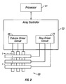
- Figure 2 is a system block diagram illustrating one embodiment of an electronic device that may incorporate aspects of the invention.
- the electronic device includes a processor 21 which may be any general purpose single- or multi-chip microprocessor such as an ARM, Pentium®, Pentium II®, Pentium III®, Pentium IV®, Pentium® Pro, an 8051, a MIPS®, a Power PC®, an ALPHA®, or any special purpose microprocessor such as a digital signal processor, microcontroller, or a programmable gate array.
- the processor 21 may be configured to execute one or more software modules.
- the processor may be configured to execute one or more software applications, including a web browser, a telephone application, an email program, or any other software application.
- the processor 21 is also configured to communicate with an array controller 22.
- the array controller 22 includes a row driver circuit 24 and a column driver circuit 26 that provide signals to a pixel array 30.
- the cross section of the array illustrated in Figure 1 is shown by the lines 1-1 in Figure 2.
- the row/column actuation protocol may take advantage of a hysteresis property of these devices illustrated in Figure 3. It may require, for example, a 10 volt potential difference to cause a movable layer to deform from the released state to the actuated state. However, when the voltage is reduced from that value, the movable layer maintains its state as the voltage drops back below 10 volts.
- the movable layer does not release completely until the voltage drops below 2 volts.
- the row/column actuation protocol can be designed such that during row strobing, pixels in the strobed row that are to be actuated are exposed to a voltage difference of about 10 volts, and pixels that are to be released are exposed to a voltage difference of close to zero volts.
- each pixel sees a potential difference within the "stability window" of 3-7 volts in this example.
- This feature makes the pixel design illustrated in Figure 1 stable under the same applied voltage conditions in either an actuated or released pre-existing state. Since each pixel of the interferometric modulator, whether in the actuated or released state, is essentially a capacitor formed by the fixed and moving reflective layers, this stable state can be held at a voltage within the hysteresis window with almost no power dissipation. Essentially no current flows into the pixel if the applied potential is fixed.
- a display frame may be created by asserting the set of column electrodes in accordance with the desired set of actuated pixels in the first row.
- a row pulse is then applied to the row 1 electrode, actuating the pixels corresponding to the asserted column lines.
- the asserted set of column electrodes is then changed to correspond to the desired set of actuated pixels in the second row.
- a pulse is then applied to the row 2 electrode, actuating the appropriate pixels in row 2 in accordance with the asserted column electrodes.
- the row 1 pixels are unaffected by the row 2 pulse, and remain in the state they were set to during the row 1 pulse. This may be repeated for the entire series of rows in a sequential fashion to produce the frame.
- the frames are refreshed and/or updated with new display data by continually repeating this process at some desired number of frames per second.
- protocols for driving row and column electrodes of pixel arrays to produce display frames are also well known and may be used in conjunction with the present invention.
- Figures 4, 5A, and 5B illustrate one possible actuation protocol for creating a display frame on the 3x3 array of Figure 2.
- Figure 4 illustrates a possible set of column and row voltage levels that may be used for pixels exhibiting the hysteresis curves of Figure 3.
- actuating a pixel involves setting the appropriate column to -V bias, and the appropriate row to + ⁇ V, which may correspond to -5 volts and +5 volts respectively Releasing the pixel is accomplished by setting the appropriate column to +V bias, and the appropriate row to the same + ⁇ V, producing a zero volt potential difference across the pixel. In those rows where the row voltage is held at zero volts, the pixels are stable in whatever state they were originally in, regardless of whether the column is at +V bias , or -V bias .
- Figure 5B is a timing diagram showing a series of row and column signals applied to the 3x3 array of Figure 2 which will result in the display arrangement illustrated in Figure 5A, where actuated pixels are non-reflective.
- the pixels Prior to writing the frame illustrated in Figure 5A, the pixels can be in any state, and in this example, all the rows are at 0 volts, and all the columns are at +5 volts. With these applied voltages, all pixels are stable in their existing actuated or released states.
- pixels (1,1), (1,2), (2,2), (3,2) and (3,3) are actuated.
- columns 1 and 2 are set to -5 volts, and column 3 is set to +5 volts. This does not change the state of any pixels, because all the pixels remain in the 3-7 volt stability window.
- Row 1 is then strobed with a pulse that goes from 0, up to 5 volts, and back to zero. This actuates the (1,1) and (1,2) pixels and releases the (1,3) pixel. No other pixels in the array are affected.
- column 2 is set to -5 volts
- columns 1 and 3 are set to +5 volts.
- Row 3 is similarly set by setting columns 2 and 3 to -5 volts, and column 1 to +5 volts.
- the row 3 strobe sets the row 3 pixels as shown in Figure 5A. After writing the frame, the row potentials are zero, and the column potentials can remain at either +5 or -5 volts, and the display is then stable in the arrangement of Figure 5A. It will be appreciated that the same procedure can be employed for arrays of dozens or hundreds of rows and columns. It will also be appreciated that the timing, sequence, and levels of voltages used to perform row and column actuation can be varied widely within the general principles outlined above, and the above example is exemplary only, and any actuation voltage method can be used with the present invention.
- Figures 6A-6C illustrate three different embodiments of the moving mirror structure.
- Figure 6A is a cross section of the embodiment of Figure 1, where a strip of metal material 14 is deposited on orthogonally extending supports 18.
- the moveable reflective material 14 is attached to supports at the comers only, on tethers 32.
- the moveable reflective material 14 is suspended from a deformable layer 34.
- This embodiment has benefits because the structural design and materials used for the reflective material 14 can be optimized with respect to the optical properties, and the structural design and materials used for the deformable layer 34 can be optimized with respect to desired mechanical properties.
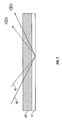
- Figure 7 is a side cross-sectional view of an interferometric modulator 12 illustrating optical paths through the modulator 12.
- the color of light reflected from the interferometric modulator 12 may vary for different angles of incidence (and reflection) as illustrated in Figure 7.
- the interferometric modulator 12 shown in Figure 7 as light travels along path A 1 , the light is incident on the interferometric modulator at a first angle, reflects from the interferometric modulator, and travels to a viewer. The viewer perceives a first color when the light reaches the viewer as a result of optical interference between a pair of mirrors in the interferometric modulator 12.
- Optical interference in the interferometric modulator 12 depends on optical path length of light propagated within the modulator. Different optical path lengths for the different optical paths A 1 and A 2 therefore yield different outputs from the interferometric modulator 12. The user therefore perceives different colors depending on his or her angle of view. This phenomenon is referred to as a "color shift".
- the amount of color shift may be expressed in terms of a difference in wavelength, e.g., in nanometers, for the light emitted from the interferometric modulators for different angles of incident (and reflected light). As is well known, for spectral reflection, the angle of incidence is equal to the angle of reflection.
- the wavelength used to measure the color shift may be the peak wavelength of the specular distribution of light output from the interferometric modulator.
- specular distribution refers to the wavelength distribution, such as for example, the intensity of light at different wavelengths.
- the output of the interferometric modulator 12 may be characterized by a spectral responsivity function or spectral response R ( ⁇ i, ⁇ ), where ⁇ i is the angle of incidence of light and ⁇ is the wavelength.
- ⁇ i is the angle of incidence of light
- ⁇ is the wavelength.
- Figure 8 schematically illustrates exemplary spectral responses R ( ⁇ i , ⁇ ) for different angles of incidence.
- a first plot 110 for example, shows a spectral response (output versus wavelength) for a first angle of incidence.
- a second plot 120 shows a spectral response for a second angle of incidence.
- the first and second plots each have peaks 115, 125, sometime referred to herein as spectral lines. These plots 110, 120 and the corresponding peaks are shifted from each other. The shift in the peaks 115, 125 for the different plots shows the color shift with angle of view.
- a certain amount of perceived off-axis color shift in a display may be tolerated for certain displays.
- a color shift or a change e.g., of about 5-30 nanometers in wavelength for an angle of view shift of about 40° may be acceptable for certain applications.
- the color shift is too significant and is noticeable by the observer.
- methods of correcting or compensating for such intolerable color shifts as described herein may be employed.
- the level of tolerance that is permissible may depend upon factors that include the intended use of the display, the quality, and/or the price range of the display.
- the level of "tolerance” in color shift may be expressed in terms of nanometers of wavelength shift for a change in view angle of a specified range.
- the tolerance may be expressed for a range between about -60° and 60°.
- the tolerance may be expressed for a range between about -80° and 80°
- a diffuser may be used to compensate for the color shift of an interferometric modulator structure.
- Figure 9 shows one embodiment of interferometric modulator display 200 that includes a diffuser layer 201.
- the interferometric modulator display 200 includes a transparent substrate 20, such as glass, having a viewing surface to which the diffuser layer 201 is attached.
- the diffuser layer 201 is formed on the top side of the substrate 20 as shown in Figure 9. Other designs are also possible.
- Diffusers may comprise bulk diffuser material.
- a diffuser may include one or more layers of a material such as a suitable transparent or translucent polymer resin, for example, polyester, polycarbonate, polyvinyl chloride (PVC), polyvinylidene chloride, polystyrene, polyacrylates, polyethylene terephthalate, polyurethane, and copolymers or blends thereof. Other materials may be employed as well.
- the diffuser is attached to a surface of the substrate using a double-sided adhesive.
- Figure 10 is a graphical diagram 300 of exemplary optical responses, referred to as D( ⁇ i , ⁇ ), for a diffuser or diffuser material in accordance embodiments of the invention.
- Output from the diffuser may depend on both angle of incidence ⁇ i and on angle of transmission or angle of view, ⁇ .
- the optical transfer function D( ⁇ i , ⁇ ) may be expressed as a function of the angle of view "0" and the angle of incidence of light " ⁇ i " ranging, e.g., from 0 to 90° or from 0 to - 90°.
- the vertical axis depicts the relative intensity of light from a light source that is observed through a diffuser.
- the horizontal axis represents the angle of viewing of light communicated through the diffuser.
- the possible angle of view varies from 0 to 90 degrees on the right side of graph and from 0 to -90 degrees ⁇ left side of graph 300).
- Curves or traces 310, 320, and 330 in Figure 10 depict the optical response of diffusers for a given angle of incidence, ⁇ i as the output varies with transmission angle or view angle ⁇ .
- This angle of incidence may, for example, be 0° for the plots 310, 320, 330 in Figure 10.
- the first trace 310 depicts the perceived intensity of light versus angle of viewing for a particular diffuser (and a particular angle of incidence).
- the trace 310 has a generally a bell-shaped curve that has a relatively sharp peak at a center angle.
- the sharp or relatively narrow peak is located at 0° for this embodiment of the diffuser.
- This narrow peak may for example have a width as measured at full width half maximum of about 10-30°.
- This type of trace is sometimes referred to as a high gain curve.
- the trace 320 depicts an optical response for a second type of diffuser.
- the trace 320 is a generally bell-shaped curve that has a relatively small wider peak at its center. This narrow peak may for example have a width as measured at full width half maximum of about 60-100°
- the trace 320 with its relatively low peak and thus somewhat flattened response profile is sometimes referred to as a low gain curve.
- each optical response is shown as centered at about 0° for the purpose of illustration. As will be discussed further below, the optical response may be centered at other angles for different diffusers.
- Figure 10 shows a trace 330 depicting the optical response of an ideal Lambertian diffuser.
- Lambertian diffusers are characterized by a substantially flat angular response profile.
- the trace 330 depicts an approximately straight line response having a generally fixed intensity at all angles of viewing.
- non-lambertian diffusers do not have substantially flat angular response profiles.
- the high gain and low gain diffusers corresponding to traces 310 and 320 are examples of non-lambertian diffusers.
- the traces 310 and 320 illustrate optical responses of various diffusers having responses that are centered around zero degrees (0°).
- similar shaped (or other shaped) response profiles may be centered on view angles other than zero degrees, such as, for example, at ten (10), twenty (20), thirty (30), forty (40), 45 (forty five), 50 (fifty), 60 (sixty), 70 (seventy), 80 (eighty) degrees, or on any other view angle.
- D( ⁇ i , ⁇ ) may be characterized by a response profile that may be different characteristically for different angles of view.
- the diffuser 201 may be a high gain, low gain (or very low gain), or any other suitable type of diffuser therebetween, or any combination thereof.
- the centering of D( ⁇ i , ⁇ ) around a particular angle is relevant to computing a convolution of D( ⁇ i , ⁇ ) and optical response of the interferometric modulator, without the diffuser, which is referred to as R ( ⁇ i , ⁇ )
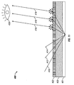
- Figure 11 is a cross-sectional view illustrating an embodiment of an interferometric modulator display 400 that includes a diffuser 402.
- the display 400 includes an array of interferometric modulators 401.
- the diffuser 402 is physically coupled to a substrate 403. Light is reflected in the interferometric modulator 401 so as to pass outward through the diffuser 402.
- the diffuser 402 is selected based on its characteristics which influence the reflected light so as to compensate for at least a portion of the angular color shift of the interferometric modulator 401. This compensation reduces the perceived color shift as the viewing angle of a user of the modulator 401 changes.
- any numerical values used herein, such as the angles of incidence of light paths 410, 412, and 414, are presented for purposes of illustration and are not necessarily indicative of any embodiment.
- the modulator 401 reflects the light further along the paths 410, 412, and 414.
- the light along the paths 410, 412, and 414 is then incident on the diffuser 402.
- the diffuser 402 redirects portions of the reflected light along a range of optical paths at intensities that depend upon the gain characteristics, D( ⁇ i , ⁇ ), of the diffuser 402.
- the diffused portion of the light from optical paths 410, 412, and 414 travels to a viewing position along optical paths 416.
- These paths 416 are at substantially the same angle with respect to the diffuser 402 and substantially parallel for this particular exemplary viewing position 430 which is a distant viewing position.
- the diffuser 402 thus operates to collect light that is incident on the modulator 401 at a range of angles and corresponding optical paths, including the paths 410, 412, and 414. This collected light is redirected. A portion of this light is redirected to the viewing position along the optical paths 416.
- the diffuser 402 thus collects light from the modulator 401 (or array of modulators 401) at a range of wavelengths to produce a net optical response for the modulator 401 as modified by the diffuser 402.
- the net optical response is related to the convolution of the optical response D( ⁇ i , ⁇ ) of the diffuser with the optical response R ( ⁇ i , ⁇ ) of the modulator 401 over a range of angles of light incident on the display 400.
- the net optical response of the system 400 can thus be controlled to achieve a desired net optical response.
- the characteristics of the diffuser 402 and the interferometric modulator 401 are selected so as to substantially compensate for angular color shift of the interferometric modulator 401.
- the characteristics of the diffuser 402 and the modulator 401 are selected so that an image formed by the modulator array alone is obscured or encrypted and is not visible. The image formed by the modulator array, however, is visible by viewing through the diffuser 402.
- the overall optical characteristics of the modulator 401 together with the diffuser 402 may be modeled in terms of the convolution of the optical response (i.e., spectral reflectance or transfer function) of the modulator 401, with the optical response of the diffuser 402.
- An exemplary expression for this convolution is set forth below.
- the optical response R ( ⁇ i , ⁇ ) of the modulator 401 is represented as a function of the angle of incidence, ⁇ i , and wavelength of light, ⁇ , entering the modulator 401.
- the angle of incidence is equal to the angle of reflection for specular reflection
- the view angle, 0, for the modulator is equal to the angle of incidence, ⁇ i , on the modulator.
- R ( ⁇ i , ⁇ ) characterizes the optical response of the modulator as a function of view angle, 0.
- the intensity of the light coming out of the diffuser 402 is also generally a function of the viewing angle ⁇ (and angle of incidence ⁇ i ). Accordingly, as described above, the optical response of the diffuser is characterized by D( ⁇ i , ⁇ ).
- the view angle, ⁇ , of the modulator corresponds to the angle of incidence, ⁇ i , of the diffuser.
- the modified spectral reflectance R' ( ⁇ , ⁇ ) that includes the effects of the diffuser 402 can be computed.
- the result is spectral response of the display for a given view angle ⁇ .
- the spectral response of the combination of the modulator 401 and the diffuser 402 can thus be computed for a particular viewing angle and corresponding viewer position.
- the spectral response for the aggregate structure comprising the modulator 401 and the diffuser 402 may be computed for multiple viewing angles and view positions to quantify color shift resulting from change in angle of view.
- R' ( ⁇ , ⁇ ) it is desirable to define the type of overall or corrected reflectance (i.e., R' ( ⁇ , ⁇ )) in terms of particular criteria, e.g., acceptable or unacceptable level of color shift. For example, if the color shift at a particular angle of view (e.g., 30 degrees) is 100 nanometers, it may be desirable to reduce such color shift to no more than 20 nanometers. In such a case, the uncompensated optical response R ( ⁇ i , ⁇ ) of the modulator 401 having an undesirable 100-nanometer color shift (e.g., at 30 degrees) may be improved with a suitable diffuser so as to provide a resultant spectral response R' ( ⁇ , ⁇ )) having an acceptable 20-nanometer color shift. It is worth noting that these numbers are chosen arbitrarily for illustrative purpose, and any tolerance level in color shift may be used in practice. For instance in certain embodiments, the level of tolerance in color shift characteristics may depend on intended use or planned viewing conditions.
- the desirable optical response R'( ⁇ , ⁇ ) is derivable from the uncompensated optical response R ( ⁇ i , ⁇ ).
- the optical response of uncompensated R ( ⁇ i , ⁇ ) and desired R '( ⁇ , ⁇ ) are known functions
- the optical response (i.e., characteristics) for D( ⁇ i , ⁇ ) can be computed from the above equation. Since the above equation has only one unknown variable, D( ⁇ i , ⁇ ) can be determined to define the suitable diffuser for providing the desired spectral responsivity R'( ⁇ , ⁇ ).
- the D( ⁇ i, ⁇ ), once solved may, for example, correspond to a diffuser having a high gain, a low gain, or a very low gain response, or other suitable characteristics.
- D( ⁇ i , ⁇ ) is determined by solving permutations of the equation above (e.g., solving the deconvolution).
- Well known mathematical and numerical methods may be employed to perform the calculations.
- diffusers may be fabricated to provide a desired optical response. Accordingly, once characteristics of D ( ⁇ i , ⁇ ) are determined, a suitable physical configuration and material of the diffuser 402 may then be determined to produce at least an approximation of the desired response profile D ( ⁇ i , ⁇ ) such that the color shift is within a desired tolerance at the target angle.
- the physical configuration may be determined using techniques such as are known in the art. Diffusers with selected properties are available, for example, from Nitto Denko, Osaka, Japan. Additional details regarding selecting a diffuser based on the spectral response of the interferometric modulator are discussed more fully below.
- the diffuser 402 is a diffuser having high gain characteristics that may be selected to reduce or compensate for the color shift.
- Figure 12A is a graphical diagram illustrating the gain of the exemplary diffuser 402 versus angle of view for an angle of incidence of 0°.
- Figure 12B is a graphical diagram illustrating the gain of the exemplary diffuser 402 versus angle of view at an angle of incidence of 10°.
- R ( ⁇ i , ⁇ ) [ 0.5 0.9 ]
- R ( 10 ° , ⁇ ) [ 0.6 0.8 ]
- the calculations are illustrated using only two angles of incidence for a single wavelength, are provided.
- the convolution is calculated for angle of incidence ranging from 0 to 10° with a step size of 10°.
- a larger range of angles may be used and the step size may be different.
- values for various wavelengths may be identified at any particular angle of incidence (or angle of view); in this example, only 0° and 10° are being used.
- wavelengths at each angle of view there are many different wavelengths at each angle of view; however only two values (0.5 and 0.9) for the wavelength, ⁇ , are provided at 0 degrees (angle of incidence ⁇ i or angle of view) for illustration only. Similarly, two values (0.6 and 0.8) for the wavelength, ⁇ , are provided at an angle of view of 10 degrees.
- R '( ⁇ , ⁇ ) the actual optical response D( ⁇ i , ⁇ ) of the diffuser 402.
- the equation above is used to compute R '( ⁇ , ⁇ ) at a desired angle of view.
- R' ( ⁇ , ⁇ ) can be computed at an angle of view of 10° (or at any desired angle of view, e.g., between 0° and 90°, in a like manner).
- the convolution is summed by varying ⁇ i from 0° to 90° to compute the total modified or compensated optical response R '( ⁇ , ⁇ ) (as corrected by the diffuser 402).
- the diffuser 402 may include more than one diffuser layer. In one such embodiment, the same diffuser characteristics may be selected for each of the diffuser layers. In another embodiment, different characteristics may be selected for each of the layers of the diffuser 402. In one embodiment, the diffuser characteristics of the diffuser 402 may be calculated by convolving the optical responses of each of the layers.
- Figure 13 illustrates a graphical diagram 500 of several spectral reflectance traces for various configurations of interferometric modulator display devices.
- the vertical axis represents a reflectance to the viewer, expressed as a percentage (from 0 to 90%).
- the horizontal axis represents the wavelength of light that is reflected by the interferometric modulator. This reflectance corresponds to the spectral responsivity e.g., R(Q, ⁇ ), R'( ⁇ , ⁇ ), described above.
- curve 510 depicts a somewhat bell-shaped curve that represents the reflectance as viewed at 0 degrees to normal from the display of one or more interferometric modulators (without the presence of a diffuser layer).
- the peak of curve 510 is at approximately 80% reflectance and is centered about 820 nm, which is in the infrared portion of the spectrum.
- Figure 13 further depicts a curve 520 that represents the reflectance of this same display as viewed at 50 degrees to normal.
- the curve 520 is shaped similarly to the curve 510 but has a peak value of reflectance of approximately 84% that is located at about 690 nm.
- Figure 13 also depicts a somewhat bell-shaped curve 530 that represents the reflectance as viewed at 0 degrees to normal from a display that includes a diffuser layer.
- the curve 530 has a peak gain of approximately 64% that is located approximately at 750 nm.
- Figure 13 depicts a curve 540 that represents the reflectance of the display having the diffuser layer as viewed at 50 degrees to normal.
- the curve 540 follows a path that is substantially the same as the path of curve 530 with a slightly smaller peak reflectance value of 62%.
- Figure 13 shows the reflectance from the modulator using input light to the interferometric modulator that is in the infrared portion of the electromagnetic spectrum at about a peak wavelength of 810 nanometers (nm).
- the 50 degree shift in viewing angle causes an approximately 120 nm color shift in the viewed response profile.
- the curves 530 and 540 illustrate the spectral reflectance of the modulator when viewed through a very low gain diffuser 302 having a full width half maximum gain between 120° and 180°.
- the curves 530 and 540 represent the convolution of the response of this very low gain diffuser with that of the interferometric modulator.
- both curves 530 and 540 peak at about the same or a similar wavelength that is horizontally between the peaks of curves 510 and 520.
- the curves thus exhibit a very minor perceived color shift (such as in the range of about 10 to 20 nm) when the viewing angle changes by fifty degrees (50°), as in this example.
- the diffuser layer As compared to the 120 nm color shift of the modulator viewed at 50° without the diffuser layer, the diffuser layer has thus been substantially compensated for the shift in viewing angle.
- the peaks of the curves 530 and 540 do not shift in color substantially with changing viewing angle.
- the peaks of curves for the modulator without the diffuser that were in the infrared portion of the spectrum are in the red portion of the spectrum with the low gain diffuser.
- the diffuser has therefore shifted the spectral responsivity of an interferometric modulator have a peak response in the infrared to a device having a peak in a visible wavelength.
- Another characteristic of the effect of the diffuser is that the peak spectral reflectance of the convoluted, e.g., perceived, light signal is reduced and spread more evenly across the spectrum.
- the color shift and the amount of the drop in peak reflectance may be controlled by selecting the desired wavelength and angle for the peak of the curve for a diffuser.
- the selected diffuser may have a response that is centered about 0°.
- the selected diffuser may have a response centered around an angle other than 0°, for example, centered at ten (10°), twenty (20), thirty (30), forty (40), 45 (forty five), 50 (fifty), 60 (sixty), 70 (seventy), 80 (eighty) degrees, or on any other view angle.
- Figure 14 is a CIE 1976 chromaticity diagram 600 that illustrates a sequence of data points that show color shift versus view angle to further illustrate the effect of the embodiment of the diffuser 401 from Figure 13.
- the horizontal and vertical axes define a chromaticity coordinate system on which spectral tri-stimulus values may be depicted.
- a sequence of data points for an interferometric modulator display without diffuser is shown on the gamut color space of the diagram along a trace 605.
- the curve of the trace 605 indicates that there is a considerable color shift for changes in the view angle.
- a single data point 610 is shown on the diagram 401 because the color shift has been substantially eliminated by use of the diffuser layer
- a diffuser can be selected having specific properties that produce a desired spectral responsivity, R '( ⁇ , ⁇ ). Examples of properties that can be varied include the shape of the optical response D( ⁇ i , ⁇ ).
- the diffuser may comprise, e.g., a non-lambertian diffuser such as a high gain, low gain, or very low gain diffuser.
- the optical response D( ⁇ i , ⁇ ) comprises a peak
- the width of this peak can be selected. For example, peaks as measured at full width half maximum may be between about 2° to 20° wide in some embodiments or between about 20 to 120 wide or larger or smaller. Peaks widths outside these ranges are also possible.
- the position of this peak can be controlled.
- the high and low gain response shown in Figure 10 are centered about 0°, in certain embodiments, diffusers having peaked optical response with peak at locations other than 0° may be used. Other properties of the diffuser may be varied as well.
- the optical responses depicted in Figure 10 are for a particular angle of incidence; however, D( ⁇ i , ⁇ ) is also a function of ⁇ i .
- the diffuser may be configured to provide different optical responses D( ⁇ ) for light incident at different angles of incidence ⁇ i .
- the diffuser may be designed such that the width and location of peaks in the optical response are different for differing angles of incidence.
- the peak may for example be located at an angle of view equal (but opposite) to the angle of incidence.
- the angle of view of the peak may be different in magnitude from the angle of incidence.
- the spectral responsivity of the interferometric modulator varies with angle, different responses for different angles of incidence may be employed to redistribute the rays to achieve the desired dependency of color on view angle. Accordingly, reduced color shift may be achieved by properly distributing the light incident on the diffuser at different angles.
- the desired spectral responsivity R' ( ⁇ , ⁇ ) may be obtained.
- Consideration of the spectral responsivity R( ⁇ i , ⁇ ) of the interferometric modulator may be used in determining the properties of such a suitable diffuser. Accordingly, a diffuser may be selected that appropriately matches the interferometric modulator so as, for example, to reduce color shift.
- the selection and/or design of the diffuser may be based on the known spectral and angular optical response of diffuser materials and architectures.
- the diffuser is selected or designed so that the convolution of the diffuser's optical response with that of the interferometric modulator 401 produces an optical response that decreases the color shift.
- the color shift as viewed from at least one target angle may be reduced to within a predetermined tolerance for a particular viewing angle and particular interferometric modulator configuration 401.
- the predetermined tolerance may be expressed as a number of nanometers of color shift.
- Holographic or diffractive optical elements may be employed as the diffuser.
- the diffusers may also be computer generated.
- the desired optical response for the diffuser is produced by selecting materials, thicknesses, and arrangement of the materials of the diffuser to produce the desired optical response for the diffuser.
- the interferometric modulator has a spectral response (e.g., for viewing angles at normal incidence) that is centered in the infrared or other non-visible wavelength.
- a spectral response having mostly non-visible components may contribute to reduced color shifting. For example 50%, 60%, 70% or more of the wavelengths under a central peak that extends in the visible may be non-visible. The diffuser may shift this peak into the visible.
- the diffuser may exhibit a response D( ⁇ i , ⁇ , ⁇ ) that is a function of wavelength.
- the diffuser includes a holographic optical element. Other types of wavelength sensitive diffusers may be employed as well.
- a back light or front light may be added to provide additional intensity at desired wavelengths.
- the use of such frequency dependent diffuser configurations and light sources provides additional flexibility in selecting a configuration that may be viewed at a selected angle with a predetermined tolerance on color shift.
- the display 400 may include interferometric modulators 401 that have varying optical responses.
- the display 400 includes three groups of interferometric modulators 401 having optical responses that, when the modulators 401 are matched with the diffuser 402 as disclosed herein, correspond to red, green, and blue to produce a color display.
- the optical response of diffuser 402 may depend on the wavelength ⁇ of light passing through the diffuser 402.
- the diffuser 402 comprises a holographic optical element.
- a combination of several diffusers may be used to provide a display with angular color shift at a selected angle that is within a predetermined tolerance.
- one or more diffusers may be used to provide a color shift that is within a predetermined tolerance for two, three, or a range of angles. Still other configurations are possible.
- an application of the interferometric modulator with diffuser is to enable encryption or obscuring of the image of a display to secure the image from unauthorized viewing.
- the diffuser moves data from an invisible portion of the spectrum, e.g., infrared, to a visible portion of the spectrum.
- the diffuser may be positioned with respect to the interferometric modulator array so that authorized viewers receive light from the display through the diffuser.
- the interferometric modulator produces an encrypted image and the diffuser is configured to decrypt the image.
- the interferometric modulator array of the display has an optical response that is selected to receive input image data and produce an output image that is difficult for the human eye to perceive, for example, in which colors are shifted such that the image is obscured.
- the diffuser is selected to shift the colors to a produce an image with colors indicative of the input image data.
- FIGS 15A and 15B are system block diagrams illustrating an embodiment of a display device 2040.
- the display device 2040 can be, for example, a cellular or mobile telephone.
- the same components of display device 2040 or slight variations thereof are also illustrative of various types of display devices such as televisions and portable media players.
- the display device 2040 includes a housing 2041, a display 2030, an antenna 2043, a speaker 2045, an input device 2048, and a microphone 2046.
- the housing 2041 is generally formed from any of a variety of manufacturing processes as are well known to those of skill in the art, including injection molding, and vacuum forming.
- the housing 2041 may be made from any of a variety of materials, including but not limited to plastic, metal, glass, rubber, and ceramic, or a combination thereof.
- the housing 2041 includes removable portions (not shown) that may be interchanged with other removable portions of different color, or containing different logos, pictures, or symbols.
- the display 2030 of exemplary display device 2040 may be any of a variety of displays, including a bi-stable display, as described herein.
- the display 2030 includes a flat-panel display, such as plasma, EL, OLED, STN LCD, or TFT LCD as described above, or a non-flat-panel display, such as a CRT or other tube device, as is well known to those of skill in the art.
- the display 2030 includes an interferometric modulator display, as described herein.
- the components of one embodiment of exemplary display device 2040 are schematically illustrated in Figure 15B.
- the illustrated exemplary display device 2040 includes a housing 2041 and can include additional components at least partially enclosed therein.
- the exemplary display device 2040 includes a network interface 2027 that includes an antenna 2043 which is coupled to a transceiver 2047.
- the transceiver 2047 is connected to the processor 2021, which is connected to conditioning hardware 2052.
- the conditioning hardware 2052 may be configured to condition a signal (e.g. filter a signal).
- the conditioning hardware 2052 is connected to a speaker 2045 and a microphone 2046.
- the processor 2021 is also connected to an input device 2048 and a driver controller 2029.
- the driver controller 2029 is coupled to a frame buffer 2028 and to the array driver 2022, which in turn is coupled to a display array 2030.
- a power supply 2050 provides power to all components as required by the particular exemplary display device 2040 design.
- the network interface 2027 includes the antenna 2043 and the transceiver 2047 so that the exemplary display device 2040 can communicate with one or more devices over a network. In one embodiment the network interface 2027 may also have some processing capabilities to relieve requirements of the processor 2021.
- the antenna 2043 is any antenna known to those of skill in the art for transmitting and receiving signals. In one embodiment, the antenna transmits and receives RF signals according to the IEEE 802.11 standard, including IEEE 802.11(a), (b), or (g). In another embodiment, the antenna transmits and receives RF signals according to the BLUETOOTH standard. In the case of a cellular telephone, the antenna is designed to receive CDMA, GSM, AMPS or other known signals that are used to communicate within a wireless cell phone network.
- the transceiver 2047 pre-processes the signals received from the antenna 2043 so that they may be received by and further manipulated by the processor 2021.
- the transceiver 2047 also processes signals received from the processor 2021 so that they may be transmitted from the exemplary display device 2040 via the antenna 2043.
- the transceiver 2047 can be replaced by a receiver.
- network interface 2027 can be replaced by an image source, which can store or generate image data to be sent to the processor 2021.
- the image source can be a digital video disc (DVD) or a hard-disc drive that contains image data, or a software module that generates image data.
- Processor 2021 generally controls the overall operation of the exemplary display device 2040.
- the processor 2021 receives data, such as compressed image data from the network interface 2027 or an image source, and processes the data into raw image data or into a format that is readily processed into raw image data.
- the processor 2021 then sends the processed data to the driver controller 2029 or to frame buffer 2028 for storage.
- Raw data typically refers to the information that identifies the image characteristics at each location within an image. For example, such image characteristics can include color, saturation, and gray-scale level.
- the processor 2021 includes a microcontroller, CPU, or logic unit to control operation of the exemplary display device 2040.
- Conditioning hardware 2052 generally includes amplifiers and filters for transmitting signals to the speaker 2045, and for receiving signals from the microphone 2046.
- Conditioning hardware 2052 may be discrete components within the exemplary display device 2040, or may be incorporated within the processor 2021 or other components.
- the driver controller 2029 takes the raw image data generated by the processor 2021 either directly from the processor 2021 or from the frame buffer 2028 and reformats the raw image data appropriately for high speed transmission to the array driver 2022. Specifically, the driver controller 2029 reformats the raw image data into a data flow having a raster-like format, such that it has a time order suitable for scanning across the display array 2030. Then the driver controller 2029 sends the formatted information to the array driver 2022.
- a driver controller 2029 such as a LCD controller, is often associated with the system processor 2021 as a stand-alone Integrated Circuit (IC), such controllers may be implemented in many ways. They may be embedded in the processor 2021 as hardware, embedded in the processor 2021 as software, or fully integrated in hardware with the array driver 2022.
- IC Integrated Circuit
- the array driver 2022 receives the formatted information from the driver controller 2029 and reformats the video data into a parallel set of waveforms that are applied many times per second to the hundreds and sometimes thousands of leads coming from the display's x-y matrix of pixels.
- driver controller 2029, array driver 2022, and display array 2030 are appropriate for any of the types of displays described herein.
- driver controller 2029 is a conventional display controller or a bi-stable display controller (e.g., an interferometric modulator controller).
- array driver 2022 is a conventional driver or a bi-stable display driver (e.g., an interferometric modulator display).
- a driver controller 2029 is integrated with the array driver 2022.
- display array 2030 is a typical display array or a bi-stable display array (e.g., a display including an array of interferometric modulators).
- the input device 2048 allows a user to control the operation of the exemplary display device 2040.
- input device 2048 includes a keypad, such as a QWERTY keyboard or a telephone keypad, a button, a switch, a touch-sensitive screen, a pressure- or heat-sensitive membrane.
- the microphone 2046 is an input device for the exemplary display device 2040. When the microphone 2046 is used to input data to the device, voice commands may be provided by a user for controlling operations of the exemplary display device 2040.
- Power supply 2050 can include a variety of energy storage devices as are well known in the art.
- power supply 2050 is a rechargeable battery, such as a nickel-cadmium battery or a lithium ion battery.
- power supply 2050 is a renewable energy source, a capacitor, or a solar cell, including a plastic solar cell, and solar-cell paint.
- power supply 2050 is configured to receive power from a wall outlet.
- control programmability resides, as described above, in a driver controller which can be located in several places in the electronic display system. In some cases control programmability resides in the array driver 2022. Those of skill in the art will recognize that the above-described optimization may be implemented in any number of hardware and/or software components and in various configurations.
Abstract
Description
- The field of the invention relates to microelectromechanical systems (MEMS).
- Microelectromechanical systems (MEMS) include micro mechanical elements, actuators, and electronics. Micromechanical elements may be created using deposition, etching, and or other micromachining processes that etch away parts of substrates and/or deposited material layers or that add layers to form electrical and electromechanical devices. One type of MEMS device is called an interferometric modulator. An interferometric modulator may comprise a pair of conductive plates, one or both of which may be transparent and/or reflective in whole or part and capable of relative motion upon application of an appropriate electrical signal. One plate may comprise a stationary layer deposited on a substrate, the other plate may comprise a metallic membrane separated from the stationary layer by an air gap. Such devices have a wide range of applications, and it would be beneficial in the art to utilize and/or modify the characteristics of these types of devices so that their features can be exploited in improving existing products and creating new products that have not yet been developed.
- The system, method, and devices of the invention each have several aspects, no single one of which is solely responsible for its desirable attributes. Without limiting the scope of this invention, its more prominent features will now be discussed briefly. After considering this discussion, and particularly after reading the section entitled "Detailed Description of Certain Embodiments" one will understand how the features of this invention provide advantages over other display devices.
- One embodiment comprises a display device that includes at least one interferometric modulator configured to reflect incident light. The at least one interferometric modulator has an optical response that depends at least in part on angle of view and wavelength of the incident light. The display device further includes a diffuser positioned in an optical path to the at least one interferometric modulator. The diffuser has an optical response that is substantially matched to the optical response of the interferometric modulator to maintain substantially the composition of color at different angles of view.
- Another embodiment is a method of fabricating a display device. The method includes selecting a diffuser having an optical response. The method further includes disposing the diffuser in front of an interferometric modulator array. The interferometric modulator array has an optical response that depends on angle of view. Selecting the diffuser includes substantially matching the optical response of the diffuser and the optical response of the interferometric modulator array to reduce angular color shift with angle-of-view of the display device. One embodiment is a display device manufactured according to this method.
- Another embodiment comprises a display device comprising means for modulating light and means for diffusing. The modulating means is configured to reflect incident light. The modulating means has an optical response that depends at least in part on angle of view and wavelength of the incident light. The diffusing means is positioned in an optical path to the modulating means. The diffusing means has an optical response that is substantially matched to the optical response of the modulating means to maintain substantially the same composition of color at different angles of view.
- Another embodiment comprises a method of displaying an image. The method comprises reflecting light from an interferometric modulator having an optical response that depends at least in part on angle of view and wavelength of the light. The method further comprises diffusing the light using a diffuser having an optical response that is substantially matched to the optical response of the intererometric modulator to maintain substantially the same composition of color at different angles of view.
- Another embodiment is a display device. The display device includes at least one interferometric modulator having a spectral responsivity that varies with angle of view, θ, such that color varies with angle of view. The display device further includes a non-lambertian diffuser positioned in an optical path to the at least one interferometric modulator. The non lambertian diffuser has an optical response that varies with angle of view. The diffuser substantially reduces variation of color with angle of view.
- Another embodiment is a method of tailoring optical properties of a display device. The display device includes an interferometric modulator having a spectral responsivity and a diffuser having an optical response. The method includes selecting at least one property of the diffuser with reference to the spectral responsivity of the interferometric modulator so as to reduce color shift of the display device.
- Another embodiment is a display system for producing an image. The system includes at least one interferometric modulator having a spectral responsivity that depends at least in part on angle of view of the display system. The system further includes a diffuser positioned in at least one optical path through the at least one interferometric modulator. The interferometric modulator is configured to at least partially encrypt the image from view. The diffuser is configured to decrypt the image.
- One embodiment is a method of limiting view of a display to authorized viewers. The method includes selecting at least one interferometric modulator having a spectral responsivity that depends at least in part on angle of view of the display. The method further includes reflecting light indicative of an image from the at least one interferometric modulator. The interferometric modulator is configured to at least partially obscure the image from view. The method further comprises diffusing the reflected light from the at least one interferometric modulator with a diffuser having an optical response, wherein the optical response of the diffuser is configured so as to decrypt the image.
- Another embodiment comprises a method of fabricating a display system for producing an image. The method comprises providing at least one interferometric modulator having a spectral responsivity that depends at least in part on angle of view of the display system. The method further comprises positioning a diffuser in at least one optical path through the at least one interferometric modulator. The interferometric modulator is configured to at least partially encrypt the image from view and the diffuser is configured to decrypt the image.
- Another embodiment also comprises a display system for producing an image. The system comprising means for modulating light and a means for diffusing the light. The modulating means has a spectral responsivity that depends at least in part on angle of view of the display system. The modulating means is configured to at least partially encrypt the image from view and the diffusing means is configured to decrypt the image.
- Another embodiment comprises a method of producing an image. The method comprises modulating light using a modulator having a spectral responsivity that depends at least in part on angle of view of the display and diffusing the light. The image is at least partially encrypted from view and diffusing the light decrypts the image.
- In other embodiments, other types of spatial light modulators may be used, particularly those exhibiting color shift as function of viewing position.
-
- Figure 1 is an isometric view depicting a portion of one embodiment of an interferometric modulator display in which a movable reflective layer of a first interferometric modulator is in a released position and a movable reflective layer of a second interferometric modulator is in an actuated position.
- Figure 2 is a system block diagram illustrating one embodiment of an electronic device incorporating a 3x3 interferometric modulator display.
- Figure 3 is a diagram of movable mirror position versus applied voltage for one exemplary embodiment of an interferometric modulator of Figure 1.
- Figure 4 is an illustration of a set of row and column voltages that may be used to drive an interferometric modulator display.
- Figure 5A illustrates one exemplary frame of display data in the 3x3 interferometric modulator display of Figure 2.
- Figure 5B illustrates one exemplary timing diagram for row and column signals that may be used to write the frame of Figure 5A.
- Figure 6A is a cross section of the device of Figure 1.
- Figure 6B is a cross section of an alternative embodiment of an interferometric modulator.
- Figure 6C is a cross section of another alternative embodiment of an interferometric modulator.
- Figure 7 is a side cross-sectional view of an interferometric modulator display illustrating optical paths through the modulator.
- Figure 8 schematically illustrates exemplary spectral responses R (θ i ,λ) or different angles of incidence.
- Figure 9 is a side cross-sectional view of an interferometric modulator display that includes a diffuser.
- Figure 10 is an exemplary graphical diagram of intensity versus view angle for various diffusers.
- Figure 11 is a cross-sectional view of the interferometric modulator display of Figure 9, also showing an example of the effect of the diffuser.
- Figures 12A and 12B are graphical diagrams illustrating the gain of an exemplary diffuser versus angle of view for light incident at two different angles.
- Figure 13 is an exemplary graphical diagram of reflectance versus wavelength of light illustrating variation in spectral responsivity of the interferometric modulators with angle and the effects of the diffuser on the variation in spectral responsivity.
- Figure 14 is a graphical diagram of color shift versus view angle illustrating an exemplary effect of the diffuser.
- Figures 15A and 15B are system block diagrams illustrating an embodiment of a visual display device comprising a plurality of interferometric modulators.
- Various embodiments of the invention describe a system and method of using a diffuser with interferometric modulator devices so as to mitigate or compensate for color shift as a function of angle of view. In one embodiment of the invention, the display includes a plurality of interferometric display elements exhibiting color shift. The display further includes at least one diffuser. Optical properties of the diffuser are selected to reduce color shift of the display for at least one range of angles.
- The following detailed description is directed to certain specific embodiments of the invention. However, the invention can be embodied in a multitude of different ways. In this description, reference is made to the drawings wherein like parts are designated with like numerals throughout. As will be apparent from the following description, the invention may be implemented in any device that is configured to display an image, whether in motion (e.g., video) or stationary (e.g., still image), and whether textual or pictorial. More particularly, it is contemplated that the invention may be implemented in or associated with a variety of electronic devices such as, but not limited to, mobile telephones, wireless devices, personal data assistants (PDAs), hand-held or portable computers, GPS receivers/navigators, cameras, MP3 players, camcorders, game consoles, wrist watches, clocks, calculators, television monitors, flat panel displays, computer monitors, auto displays (e.g., odometer display, etc.), cockpit controls and/or displays, display of camera views (e.g., display of a rear view camera in a vehicle), electronic photographs, electronic billboards or signs, projectors, architectural structures, packaging, and aesthetic structures (e.g., display of images on a piece of jewelry). MEMS devices of similar structure to those described herein can also be used in non-display applications such as in electronic switching devices.
- One interferometric modulator display embodiment comprising an interferometric MEMS display element is illustrated in Figure 1. In these devices, the pixels are in either a bright or dark state. In the bright ("on" or "open") state, the display element reflects a large portion of incident visible light to a user. When in the dark ("off' or "closed") state, the display element reflects little incident visible light to the user. Depending on the embodiment, the light reflectance properties of the "on" and "off" states may be reversed. MEMS pixels can be configured to reflect predominantly at selected colors, allowing for a color display in addition to black and white.
- Figure 1 is an isometric view depicting two adjacent pixels in a series of pixels of a visual display, wherein each pixel comprises a MEMS interferometric modulator. In some embodiments, an interferometric modulator display comprises a row/column array of these interferometric modulators. Each interferometric modulator includes a pair of reflective layers positioned at a variable and controllable distance from each other to form a resonant optical cavity with at least one variable dimension. In one embodiment, one of the reflective layers may be moved between two positions. In the first position, referred to herein as the released state, the movable layer is positioned at a relatively large distance from a fixed partially reflective layer. In the second position, the movable layer is positioned more closely adjacent to the partially reflective layer. Incident light that reflects from the two layers interferes constructively or destructively depending on the position of the movable reflective layer, producing either an overall reflective or non-reflective state for each pixel.
- The depicted portion of the pixel array in Figure 1 includes two adjacent
interferometric modulators interferometric modulator 12a on the left, a movable and highlyreflective layer 14a is illustrated in a released position at a predetermined distance from a fixed partiallyreflective layer 16a. In theinterferometric modulator 12b on the right, the movable highlyreflective layer 14b is illustrated in an actuated position adjacent to the fixed partiallyreflective layer 16b. - The
fixed layers transparent substrate 20. The layers are patterned into parallel strips, and may form row electrodes in a display device as described further below. Themovable layers row electrodes posts 18 and an intervening sacrificial material deposited between theposts 18. When the sacrificial material is etched away, the deformable metal layers are separated from the fixed metal layers by a definedair gap 19. A highly conductive and reflective material such as aluminum may be used for the deformable layers, and these strips may form column electrodes in a display device. - With no applied voltage, the
cavity 19 remains between thelayers pixel 12a in Figure 1. However, when a potential difference is applied to a selected row and column, the capacitor formed at the intersection of the row and column electrodes at the corresponding pixel becomes charged, and electrostatic forces pull the electrodes together. If the voltage is high enough, the movable layer is deformed and is forced against the fixed layer (a dielectric material which is not illustrated in this Figure may be deposited on the fixed layer to prevent shorting and control the separation distance) as illustrated by thepixel 12b on the right in Figure 1. The behavior is the same regardless of the polarity of the applied potential difference. In this way, row/column actuation that can control the reflective vs. non-reflective pixel states is analogous in many ways to that used in conventional LCD and other display technologies. - Figures 2 through 5B illustrate one exemplary process and system for using an array of interferometric modulators in a display application. Figure 2 is a system block diagram illustrating one embodiment of an electronic device that may incorporate aspects of the invention. In the exemplary embodiment, the electronic device includes a
processor 21 which may be any general purpose single- or multi-chip microprocessor such as an ARM, Pentium®, Pentium II®, Pentium III®, Pentium IV®, Pentium® Pro, an 8051, a MIPS®, a Power PC®, an ALPHA®, or any special purpose microprocessor such as a digital signal processor, microcontroller, or a programmable gate array. As is conventional in the art, theprocessor 21 may be configured to execute one or more software modules. In addition to executing an operating system, the processor may be configured to execute one or more software applications, including a web browser, a telephone application, an email program, or any other software application. - In one embodiment, the
processor 21 is also configured to communicate with anarray controller 22. In one embodiment, thearray controller 22 includes arow driver circuit 24 and acolumn driver circuit 26 that provide signals to apixel array 30. The cross section of the array illustrated in Figure 1 is shown by the lines 1-1 in Figure 2. For MEMS interferometric modulators, the row/column actuation protocol may take advantage of a hysteresis property of these devices illustrated in Figure 3. It may require, for example, a 10 volt potential difference to cause a movable layer to deform from the released state to the actuated state. However, when the voltage is reduced from that value, the movable layer maintains its state as the voltage drops back below 10 volts. In the exemplary embodiment of Figure 3, the movable layer does not release completely until the voltage drops below 2 volts. There is thus a range of voltage, about 3 to 7 V in the example illustrated in Figure 3, where there exists a window of applied voltage within which the device is stable in either the released or actuated state. This is referred to herein as the "hysteresis window" or "stability window." For a display array having the hysteresis characteristics of Figure 3, the row/column actuation protocol can be designed such that during row strobing, pixels in the strobed row that are to be actuated are exposed to a voltage difference of about 10 volts, and pixels that are to be released are exposed to a voltage difference of close to zero volts. After the strobe, the pixels are exposed to a steady state voltage difference of about 5 volts such that they remain in whatever state the row strobe put them in. After being written, each pixel sees a potential difference within the "stability window" of 3-7 volts in this example. This feature makes the pixel design illustrated in Figure 1 stable under the same applied voltage conditions in either an actuated or released pre-existing state. Since each pixel of the interferometric modulator, whether in the actuated or released state, is essentially a capacitor formed by the fixed and moving reflective layers, this stable state can be held at a voltage within the hysteresis window with almost no power dissipation. Essentially no current flows into the pixel if the applied potential is fixed. - In typical applications, a display frame may be created by asserting the set of column electrodes in accordance with the desired set of actuated pixels in the first row. A row pulse is then applied to the
row 1 electrode, actuating the pixels corresponding to the asserted column lines. The asserted set of column electrodes is then changed to correspond to the desired set of actuated pixels in the second row. A pulse is then applied to therow 2 electrode, actuating the appropriate pixels inrow 2 in accordance with the asserted column electrodes. Therow 1 pixels are unaffected by therow 2 pulse, and remain in the state they were set to during therow 1 pulse. This may be repeated for the entire series of rows in a sequential fashion to produce the frame. Generally, the frames are refreshed and/or updated with new display data by continually repeating this process at some desired number of frames per second. A wide variety of protocols for driving row and column electrodes of pixel arrays to produce display frames are also well known and may be used in conjunction with the present invention. - Figures 4, 5A, and 5B illustrate one possible actuation protocol for creating a display frame on the 3x3 array of Figure 2. Figure 4 illustrates a possible set of column and row voltage levels that may be used for pixels exhibiting the hysteresis curves of Figure 3. In the Figure 4 embodiment, actuating a pixel involves setting the appropriate column to -Vbias, and the appropriate row to +ΔV, which may correspond to -5 volts and +5 volts respectively Releasing the pixel is accomplished by setting the appropriate column to +Vbias, and the appropriate row to the same +ΔV, producing a zero volt potential difference across the pixel. In those rows where the row voltage is held at zero volts, the pixels are stable in whatever state they were originally in, regardless of whether the column is at +Vbias, or -Vbias.
- Figure 5B is a timing diagram showing a series of row and column signals applied to the 3x3 array of Figure 2 which will result in the display arrangement illustrated in Figure 5A, where actuated pixels are non-reflective. Prior to writing the frame illustrated in Figure 5A, the pixels can be in any state, and in this example, all the rows are at 0 volts, and all the columns are at +5 volts. With these applied voltages, all pixels are stable in their existing actuated or released states.
- In the Figure 5A frame, pixels (1,1), (1,2), (2,2), (3,2) and (3,3) are actuated. To accomplish this, during a "line time" for
row 1,columns column 3 is set to +5 volts. This does not change the state of any pixels, because all the pixels remain in the 3-7 volt stability window.Row 1 is then strobed with a pulse that goes from 0, up to 5 volts, and back to zero. This actuates the (1,1) and (1,2) pixels and releases the (1,3) pixel. No other pixels in the array are affected. To setrow 2 as desired,column 2 is set to -5 volts, andcolumns Row 3 is similarly set by settingcolumns column 1 to +5 volts. Therow 3 strobe sets therow 3 pixels as shown in Figure 5A. After writing the frame, the row potentials are zero, and the column potentials can remain at either +5 or -5 volts, and the display is then stable in the arrangement of Figure 5A. It will be appreciated that the same procedure can be employed for arrays of dozens or hundreds of rows and columns. It will also be appreciated that the timing, sequence, and levels of voltages used to perform row and column actuation can be varied widely within the general principles outlined above, and the above example is exemplary only, and any actuation voltage method can be used with the present invention. - The details of the structure of interferometric modulators that operate in accordance with the principles set forth above may vary widely. For example, Figures 6A-6C illustrate three different embodiments of the moving mirror structure. Figure 6A is a cross section of the embodiment of Figure 1, where a strip of
metal material 14 is deposited on orthogonally extending supports 18. In Figure 6B, the moveablereflective material 14 is attached to supports at the comers only, ontethers 32. In Figure 6C, the moveablereflective material 14 is suspended from adeformable layer 34. This embodiment has benefits because the structural design and materials used for thereflective material 14 can be optimized with respect to the optical properties, and the structural design and materials used for thedeformable layer 34 can be optimized with respect to desired mechanical properties. The production of various types of interferometric devices is described in a variety of published documents, including, for example, U.S. Published Application 2004/0051929. A wide variety of well known techniques may be used to produce the above described structures involving a series of material deposition, patterning, and etching steps. - Figure 7 is a side cross-sectional view of an
interferometric modulator 12 illustrating optical paths through themodulator 12. The color of light reflected from theinterferometric modulator 12 may vary for different angles of incidence (and reflection) as illustrated in Figure 7. For example, for theinterferometric modulator 12 shown in Figure 7, as light travels along path A1, the light is incident on the interferometric modulator at a first angle, reflects from the interferometric modulator, and travels to a viewer. The viewer perceives a first color when the light reaches the viewer as a result of optical interference between a pair of mirrors in theinterferometric modulator 12. When the viewer moves or changes his/her location and thus view angle, the light received by the viewer travels along a different path A2 having corresponding a second different angle of incident (and reflection). Optical interference in theinterferometric modulator 12 depends on optical path length of light propagated within the modulator. Different optical path lengths for the different optical paths A1 and A2 therefore yield different outputs from theinterferometric modulator 12. The user therefore perceives different colors depending on his or her angle of view. This phenomenon is referred to as a "color shift". - The amount of color shift may be expressed in terms of a difference in wavelength, e.g., in nanometers, for the light emitted from the interferometric modulators for different angles of incident (and reflected light). As is well known, for spectral reflection, the angle of incidence is equal to the angle of reflection. The wavelength used to measure the color shift may be the peak wavelength of the specular distribution of light output from the interferometric modulator. As used to herein, specular distribution refers to the wavelength distribution, such as for example, the intensity of light at different wavelengths.
- The output of the
interferometric modulator 12 may be characterized by a spectral responsivity function or spectral response R(θi, λ), where θi is the angle of incidence of light and λ is the wavelength. As described above, the spectral output of theinterferometric modulator 12 varies with angle of incidence (and angle of reflection). Figure 8 schematically illustrates exemplary spectral responses R(θ i , λ) for different angles of incidence. Afirst plot 110, for example, shows a spectral response (output versus wavelength) for a first angle of incidence. Asecond plot 120 shows a spectral response for a second angle of incidence. The first and second plots each have peaks 115, 125, sometime referred to herein as spectral lines. Theseplots peaks - Generally, a certain amount of perceived off-axis color shift in a display may be tolerated for certain displays. A color shift or a change, e.g., of about 5-30 nanometers in wavelength for an angle of view shift of about 40° may be acceptable for certain applications. However, in some cases, the color shift is too significant and is noticeable by the observer. In such a case, methods of correcting or compensating for such intolerable color shifts as described herein may be employed. In practice, the level of tolerance that is permissible may depend upon factors that include the intended use of the display, the quality, and/or the price range of the display. As indicated above, the level of "tolerance" in color shift may be expressed in terms of nanometers of wavelength shift for a change in view angle of a specified range. For example, in one embodiment, the tolerance may be expressed for a range between about -60° and 60°. In another embodiment, for example, a display used as part of signage, the tolerance may be expressed for a range between about -80° and 80°
- In certain preferred embodiments, a diffuser may be used to compensate for the color shift of an interferometric modulator structure. Figure 9 shows one embodiment of
interferometric modulator display 200 that includes adiffuser layer 201. Theinterferometric modulator display 200 includes atransparent substrate 20, such as glass, having a viewing surface to which thediffuser layer 201 is attached. In one embodiment, for example, thediffuser layer 201 is formed on the top side of thesubstrate 20 as shown in Figure 9. Other designs are also possible. - Diffusers may comprise bulk diffuser material. For example, a diffuser may include one or more layers of a material such as a suitable transparent or translucent polymer resin, for example, polyester, polycarbonate, polyvinyl chloride (PVC), polyvinylidene chloride, polystyrene, polyacrylates, polyethylene terephthalate, polyurethane, and copolymers or blends thereof. Other materials may be employed as well. In one embodiment, the diffuser is attached to a surface of the substrate using a double-sided adhesive.
- Figure 10 is a graphical diagram 300 of exemplary optical responses, referred to as D(θi, θ), for a diffuser or diffuser material in accordance embodiments of the invention. Output from the diffuser may depend on both angle of incidence θi and on angle of transmission or angle of view, θ. Accordingly, the optical transfer function D(θi, θ) may be expressed as a function of the angle of view "0" and the angle of incidence of light "θi" ranging, e.g., from 0 to 90° or from 0 to - 90°.
- As shown in Figure 10, the vertical axis depicts the relative intensity of light from a light source that is observed through a diffuser. The horizontal axis represents the angle of viewing of light communicated through the diffuser. The possible angle of view varies from 0 to 90 degrees on the right side of graph and from 0 to -90 degrees ― left side of graph 300).
- Curves or traces 310, 320, and 330 in Figure 10 depict the optical response of diffusers for a given angle of incidence, θi as the output varies with transmission angle or view angle θ. This angle of incidence may, for example, be 0° for the
plots plots - As further shown in Figure 10, the
first trace 310 depicts the perceived intensity of light versus angle of viewing for a particular diffuser (and a particular angle of incidence). In one embodiment, thetrace 310 has a generally a bell-shaped curve that has a relatively sharp peak at a center angle. The sharp or relatively narrow peak is located at 0° for this embodiment of the diffuser. This narrow peak may for example have a width as measured at full width half maximum of about 10-30°. This type of trace is sometimes referred to as a high gain curve. - The
trace 320 depicts an optical response for a second type of diffuser. Thetrace 320 is a generally bell-shaped curve that has a relatively small wider peak at its center. This narrow peak may for example have a width as measured at full width half maximum of about 60-100° Thetrace 320, with its relatively low peak and thus somewhat flattened response profile is sometimes referred to as a low gain curve. As shown in connection with thetraces - Finally, Figure 10 shows a
trace 330 depicting the optical response of an ideal Lambertian diffuser. Lambertian diffusers are characterized by a substantially flat angular response profile. Thus, thetrace 330 depicts an approximately straight line response having a generally fixed intensity at all angles of viewing. Conversely, non-lambertian diffusers do not have substantially flat angular response profiles. The high gain and low gain diffusers corresponding totraces - As discussed above, the
traces - Accordingly, D(θi, θ) may be characterized by a response profile that may be different characteristically for different angles of view. In various embodiments, for example, the
diffuser 201 may be a high gain, low gain (or very low gain), or any other suitable type of diffuser therebetween, or any combination thereof. As will be apparent from the following discussion, the centering of D(θi, θ) around a particular angle is relevant to computing a convolution of D(θi, θ) and optical response of the interferometric modulator, without the diffuser, which is referred to as R(θi ,λ) - Figure 11 is a cross-sectional view illustrating an embodiment of an
interferometric modulator display 400 that includes adiffuser 402. In one embodiment, thedisplay 400 includes an array ofinterferometric modulators 401. In certain embodiments, thediffuser 402 is physically coupled to asubstrate 403. Light is reflected in theinterferometric modulator 401 so as to pass outward through thediffuser 402. As described in further detail below, thediffuser 402 is selected based on its characteristics which influence the reflected light so as to compensate for at least a portion of the angular color shift of theinterferometric modulator 401. This compensation reduces the perceived color shift as the viewing angle of a user of the modulator 401 changes. In operation, light from the light source (not shown) is incident on themodulator 401 along optical paths such asexemplary paths optical paths light paths - The
modulator 401 reflects the light further along thepaths paths diffuser 402. Thediffuser 402 redirects portions of the reflected light along a range of optical paths at intensities that depend upon the gain characteristics, D(θi, θ), of thediffuser 402. The diffused portion of the light fromoptical paths optical paths 416. Thesepaths 416 are at substantially the same angle with respect to thediffuser 402 and substantially parallel for this particularexemplary viewing position 430 which is a distant viewing position. - The
diffuser 402 thus operates to collect light that is incident on themodulator 401 at a range of angles and corresponding optical paths, including thepaths optical paths 416. - The
diffuser 402 thus collects light from the modulator 401 (or array of modulators 401) at a range of wavelengths to produce a net optical response for themodulator 401 as modified by thediffuser 402. The net optical response is related to the convolution of the optical response D(θi, θ) of the diffuser with the optical response R(θi, λ) of themodulator 401 over a range of angles of light incident on thedisplay 400. - By controlling the characteristics, e.g., D(θi, θ), of the
diffuser 402 in conjunction with optical response of themodulator 401, the net optical response of thesystem 400 can thus be controlled to achieve a desired net optical response. In one embodiment, the characteristics of thediffuser 402 and theinterferometric modulator 401 are selected so as to substantially compensate for angular color shift of theinterferometric modulator 401. In another embodiment, the characteristics of thediffuser 402 and themodulator 401 are selected so that an image formed by the modulator array alone is obscured or encrypted and is not visible. The image formed by the modulator array, however, is visible by viewing through thediffuser 402. - The overall optical characteristics of the
modulator 401 together with thediffuser 402 may be modeled in terms of the convolution of the optical response (i.e., spectral reflectance or transfer function) of themodulator 401, with the optical response of thediffuser 402. An exemplary expression for this convolution is set forth below. - As noted above, the optical response R(θ i , λ) of the
modulator 401 is represented as a function of the angle of incidence, θi, and wavelength of light, λ, entering themodulator 401. As the angle of incidence is equal to the angle of reflection for specular reflection, the view angle, 0, for the modulator is equal to the angle of incidence, θi, on the modulator. Hence, R(θi, λ) characterizes the optical response of the modulator as a function of view angle, 0. - The intensity of the light coming out of the
diffuser 402 is also generally a function of the viewing angle θ (and angle of incidence θi). Accordingly, as described above, the optical response of the diffuser is characterized by D(θi, θ). - For the combination of the
modulator 401 and thediffuser 402, the view angle, θ, of the modulator corresponds to the angle of incidence, θi, of the diffuser. Thus, the total or net optical response of themodulator 401 as modified by the diffuser 402 (see Fig. 11) may be expressed as R'(θ, λ) in accordance with the following relation:
- Using the above equation, the modified spectral reflectance R' (θ ,λ) that includes the effects of the
diffuser 402 can be computed. The summation is performed for a range of angles θi (i.e., for θi = 0 to 90 degrees) in determining the responsivity R'(θ,λ) . The result is spectral response of the display for a given view angle θ. - The spectral response of the combination of the
modulator 401 and thediffuser 402 can thus be computed for a particular viewing angle and corresponding viewer position. Similarly, the spectral response for the aggregate structure comprising themodulator 401 and thediffuser 402 may be computed for multiple viewing angles and view positions to quantify color shift resulting from change in angle of view. - In one embodiment, it is desirable to define the type of overall or corrected reflectance (i.e., R'(θ, λ)) in terms of particular criteria, e.g., acceptable or unacceptable level of color shift. For example, if the color shift at a particular angle of view (e.g., 30 degrees) is 100 nanometers, it may be desirable to reduce such color shift to no more than 20 nanometers. In such a case, the uncompensated optical response R(θi,λ) of the
modulator 401 having an undesirable 100-nanometer color shift (e.g., at 30 degrees) may be improved with a suitable diffuser so as to provide a resultant spectral responseR'(θ,λ)) having an acceptable 20-nanometer color shift. It is worth noting that these numbers are chosen arbitrarily for illustrative purpose, and any tolerance level in color shift may be used in practice. For instance in certain embodiments, the level of tolerance in color shift characteristics may depend on intended use or planned viewing conditions. - Accordingly, the desirable optical response R'(θ,λ) is derivable from the uncompensated optical response R(θi, λ). In this case, since the optical response of uncompensated R( θi, λ) and desired R'(θ, λ) are known functions, the optical response (i.e., characteristics) for D(θi, θ) can be computed from the above equation. Since the above equation has only one unknown variable, D(θi, θ) can be determined to define the suitable diffuser for providing the desired spectral responsivity R'(θ, λ). The D(θi, θ), once solved may, for example, correspond to a diffuser having a high gain, a low gain, or a very low gain response, or other suitable characteristics.
- In one embodiment, D(θi, θ) is determined by solving permutations of the equation above (e.g., solving the deconvolution). Well known mathematical and numerical methods may be employed to perform the calculations.
- As is well known in the art, diffusers may be fabricated to provide a desired optical response. Accordingly, once characteristics of D (θ i ,θ) are determined, a suitable physical configuration and material of the
diffuser 402 may then be determined to produce at least an approximation of the desired response profile D(θ i ,θ) such that the color shift is within a desired tolerance at the target angle. In various embodiments, the physical configuration may be determined using techniques such as are known in the art. Diffusers with selected properties are available, for example, from Nitto Denko, Osaka, Japan. Additional details regarding selecting a diffuser based on the spectral response of the interferometric modulator are discussed more fully below. - To illustrate application of this optical model, calculations for determining the spectral response R'(θ, λ) of the combination of the
modulator 401 anddiffuser 402 based on the known spectral response R(θi, λ) of themodulator 401 and the known optical response D ( θ i ,θ ) of the diffuser are provided. - In one embodiment, for example, the
diffuser 402 is a diffuser having high gain characteristics that may be selected to reduce or compensate for the color shift. Figure 12A is a graphical diagram illustrating the gain of theexemplary diffuser 402 versus angle of view for an angle of incidence of 0°. Figure 12B is a graphical diagram illustrating the gain of theexemplary diffuser 402 versus angle of view at an angle of incidence of 10°. In this illustration, it may be assumed that the following values for R(θi, λ) are derived from the curve of the optical response (not shown):

- In this example, the calculations are illustrated using only two angles of incidence for a single wavelength, are provided. In particular, the convolution is calculated for angle of incidence ranging from 0 to 10° with a step size of 10°. In practice, a larger range of angles may be used and the step size may be different. Likewise, it is to be understood that, values for various wavelengths may be identified at any particular angle of incidence (or angle of view); in this example, only 0° and 10° are being used.
- Also, there are many different wavelengths at each angle of view; however only two values (0.5 and 0.9) for the wavelength, λ, are provided at 0 degrees (angle of incidence θi or angle of view) for illustration only. Similarly, two values (0.6 and 0.8) for the wavelength, λ, are provided at an angle of view of 10 degrees.
- To verify that the selected
diffuser 402 performs the intended color shift compensation, for example, one may compute R'(θ, λ) using the actual optical response D(θi, θ) of thediffuser 402. To determine such compensated optical response R'(θ, λ) of themodulator 401 as modified by thediffuser 402, the equation above is used to compute R'(θ, λ) at a desired angle of view. In this example, the optical response D(θi, θ) is used and it is assumed that D(0°, 10°) = 0.5 and D(10°, 10°) = 0.2 to compute the effect of thediffuser 402 at an angle ofview 10°. It is to be recognized that these numbers have been selected arbitrarily to illustrate the principle described herein and are not limiting. Moreover, as discussed above, the convolution may be performed for a greater number of angles of incidence θi, even though in this numeric example only values at two values of θi; are provided for D(θi, θ), i.e., 0.2 and 0.5. - In performing the convolution of D(θi, θ) with R(θi, λ), R'(θ, λ) can be computed at an angle of view of 10° (or at any desired angle of view, e.g., between 0° and 90°, in a like manner). In performing the convolution in this particular example, each value for D(θi, θ) that is used is obtained from the D(θi, θ) curve at the angle of view (in this example, θ = 10°) for all values of θi.
- As noted above, for each angle of view computation, the convolution is summed by varying θi from 0° to 90° to compute the total modified or compensated optical response R'(θ, λ) (as corrected by the diffuser 402). In this numeric example, the computation may operate as follows:

- In some embodiments, the
diffuser 402 may include more than one diffuser layer. In one such embodiment, the same diffuser characteristics may be selected for each of the diffuser layers. In another embodiment, different characteristics may be selected for each of the layers of thediffuser 402. In one embodiment, the diffuser characteristics of thediffuser 402 may be calculated by convolving the optical responses of each of the layers. - Figure 13 illustrates a graphical diagram 500 of several spectral reflectance traces for various configurations of interferometric modulator display devices. As shown in Figure 13, the vertical axis represents a reflectance to the viewer, expressed as a percentage (from 0 to 90%). The horizontal axis represents the wavelength of light that is reflected by the interferometric modulator. This reflectance corresponds to the spectral responsivity e.g., R(Q, λ), R'(θ, λ), described above.
- As further shown in Figure 13,
curve 510 depicts a somewhat bell-shaped curve that represents the reflectance as viewed at 0 degrees to normal from the display of one or more interferometric modulators (without the presence of a diffuser layer). The peak ofcurve 510 is at approximately 80% reflectance and is centered about 820 nm, which is in the infrared portion of the spectrum. - Figure 13 further depicts a
curve 520 that represents the reflectance of this same display as viewed at 50 degrees to normal. Thecurve 520 is shaped similarly to thecurve 510 but has a peak value of reflectance of approximately 84% that is located at about 690 nm. - Figure 13 also depicts a somewhat bell-shaped
curve 530 that represents the reflectance as viewed at 0 degrees to normal from a display that includes a diffuser layer. Thecurve 530 has a peak gain of approximately 64% that is located approximately at 750 nm. Figure 13 depicts acurve 540 that represents the reflectance of the display having the diffuser layer as viewed at 50 degrees to normal. Thecurve 540 follows a path that is substantially the same as the path ofcurve 530 with a slightly smaller peak reflectance value of 62%. - Figure 13 shows the reflectance from the modulator using input light to the interferometric modulator that is in the infrared portion of the electromagnetic spectrum at about a peak wavelength of 810 nanometers (nm). As can be seen by comparing the
curves curves curves curves curves - As compared to the 120 nm color shift of the modulator viewed at 50° without the diffuser layer, the diffuser layer has thus been substantially compensated for the shift in viewing angle. The peaks of the
curves - Additionally, the peaks of curves for the modulator without the diffuser that were in the infrared portion of the spectrum are in the red portion of the spectrum with the low gain diffuser. The diffuser has therefore shifted the spectral responsivity of an interferometric modulator have a peak response in the infrared to a device having a peak in a visible wavelength. Another characteristic of the effect of the diffuser is that the peak spectral reflectance of the convoluted, e.g., perceived, light signal is reduced and spread more evenly across the spectrum.
- The color shift and the amount of the drop in peak reflectance may be controlled by selecting the desired wavelength and angle for the peak of the curve for a diffuser. In one embodiment, the selected diffuser may have a response that is centered about 0°. In other embodiments, the selected diffuser may have a response centered around an angle other than 0°, for example, centered at ten (10°), twenty (20), thirty (30), forty (40), 45 (forty five), 50 (fifty), 60 (sixty), 70 (seventy), 80 (eighty) degrees, or on any other view angle.
- Figure 14, is a
CIE 1976 chromaticity diagram 600 that illustrates a sequence of data points that show color shift versus view angle to further illustrate the effect of the embodiment of thediffuser 401 from Figure 13. The horizontal and vertical axes define a chromaticity coordinate system on which spectral tri-stimulus values may be depicted. A sequence of data points for an interferometric modulator display without diffuser is shown on the gamut color space of the diagram along atrace 605. The curve of thetrace 605 indicates that there is a considerable color shift for changes in the view angle. For the interferometric modulator display with the very low gain response, such as shown intraces single data point 610 is shown on the diagram 401 because the color shift has been substantially eliminated by use of the diffuser layer - More generally, a diffuser can be selected having specific properties that produce a desired spectral responsivity, R'(θ, λ). Examples of properties that can be varied include the shape of the optical response D(θi, θ). As discussed above, the diffuser may comprise, e.g., a non-lambertian diffuser such as a high gain, low gain, or very low gain diffuser. In the case where the optical response D(θi, θ) comprises a peak, the width of this peak can be selected. For example, peaks as measured at full width half maximum may be between about 2° to 20° wide in some embodiments or between about 20 to 120 wide or larger or smaller. Peaks widths outside these ranges are also possible. In addition, the position of this peak can be controlled. Although the high and low gain response shown in Figure 10 are centered about 0°, in certain embodiments, diffusers having peaked optical response with peak at locations other than 0° may be used. Other properties of the diffuser may be varied as well.
- For example, the optical responses depicted in Figure 10 are for a particular angle of incidence; however, D(θi, θ) is also a function of θi. In various embodiments, therefore, the diffuser may be configured to provide different optical responses D(θ) for light incident at different angles of incidence θi. For example, the diffuser may be designed such that the width and location of peaks in the optical response are different for differing angles of incidence. The peak may for example be located at an angle of view equal (but opposite) to the angle of incidence. Alternatively, the angle of view of the peak may be different in magnitude from the angle of incidence.
- Since the spectral responsivity of the interferometric modulator varies with angle, different responses for different angles of incidence may be employed to redistribute the rays to achieve the desired dependency of color on view angle. Accordingly, reduced color shift may be achieved by properly distributing the light incident on the diffuser at different angles.
- Thus, by selecting the different features of the optical response D(θi, θ), the desired spectral responsivity R'(θ,λ) may be obtained. Consideration of the spectral responsivity R(θi, λ) of the interferometric modulator may be used in determining the properties of such a suitable diffuser. Accordingly, a diffuser may be selected that appropriately matches the interferometric modulator so as, for example, to reduce color shift.
- As described above, using techniques known in the art, the selection and/or design of the diffuser may be based on the known spectral and angular optical response of diffuser materials and architectures. In particular, the diffuser is selected or designed so that the convolution of the diffuser's optical response with that of the
interferometric modulator 401 produces an optical response that decreases the color shift. Thus, the color shift as viewed from at least one target angle may be reduced to within a predetermined tolerance for a particular viewing angle and particularinterferometric modulator configuration 401. The predetermined tolerance may be expressed as a number of nanometers of color shift. - Holographic or diffractive optical elements may be employed as the diffuser. The diffusers may also be computer generated. In one embodiment, the desired optical response for the diffuser is produced by selecting materials, thicknesses, and arrangement of the materials of the diffuser to produce the desired optical response for the diffuser.
- In certain embodiments, the interferometric modulator has a spectral response (e.g., for viewing angles at normal incidence) that is centered in the infrared or other non-visible wavelength. Such a spectral response having mostly non-visible components may contribute to reduced color shifting. For example 50%, 60%, 70% or more of the wavelengths under a central peak that extends in the visible may be non-visible. The diffuser may shift this peak into the visible.
- In certain embodiments, the diffuser may exhibit a response D(θi, θ, λ) that is a function of wavelength. In one embodiment, the diffuser includes a holographic optical element. Other types of wavelength sensitive diffusers may be employed as well.
- In addition, in embodiments where a shift to the blue end of the spectrum is desired, a back light or front light may be added to provide additional intensity at desired wavelengths. The use of such frequency dependent diffuser configurations and light sources provides additional flexibility in selecting a configuration that may be viewed at a selected angle with a predetermined tolerance on color shift.
- In one embodiment, the
display 400 may includeinterferometric modulators 401 that have varying optical responses. For example, in one embodiment thedisplay 400 includes three groups ofinterferometric modulators 401 having optical responses that, when themodulators 401 are matched with thediffuser 402 as disclosed herein, correspond to red, green, and blue to produce a color display. In one such embodiment, the optical response ofdiffuser 402 may depend on the wavelength λ of light passing through thediffuser 402. In one such embodiment, thediffuser 402 comprises a holographic optical element. - Variations in the design of the display are possible. For example, in some embodiments, a combination of several diffusers may be used to provide a display with angular color shift at a selected angle that is within a predetermined tolerance. In another embodiment, one or more diffusers may be used to provide a color shift that is within a predetermined tolerance for two, three, or a range of angles. Still other configurations are possible.
- In one embodiment, an application of the interferometric modulator with diffuser is to enable encryption or obscuring of the image of a display to secure the image from unauthorized viewing. In one embodiment, the diffuser moves data from an invisible portion of the spectrum, e.g., infrared, to a visible portion of the spectrum. The diffuser may be positioned with respect to the interferometric modulator array so that authorized viewers receive light from the display through the diffuser.
- Thus, in such an embodiment, the interferometric modulator produces an encrypted image and the diffuser is configured to decrypt the image. In another embodiment, the interferometric modulator array of the display has an optical response that is selected to receive input image data and produce an output image that is difficult for the human eye to perceive, for example, in which colors are shifted such that the image is obscured. The diffuser is selected to shift the colors to a produce an image with colors indicative of the input image data.
- Figures 15A and 15B are system block diagrams illustrating an embodiment of a
display device 2040. Thedisplay device 2040 can be, for example, a cellular or mobile telephone. However, the same components ofdisplay device 2040 or slight variations thereof are also illustrative of various types of display devices such as televisions and portable media players. - The
display device 2040 includes ahousing 2041, adisplay 2030, anantenna 2043, aspeaker 2045, aninput device 2048, and amicrophone 2046. Thehousing 2041 is generally formed from any of a variety of manufacturing processes as are well known to those of skill in the art, including injection molding, and vacuum forming. In addition, thehousing 2041 may be made from any of a variety of materials, including but not limited to plastic, metal, glass, rubber, and ceramic, or a combination thereof. In one embodiment thehousing 2041 includes removable portions (not shown) that may be interchanged with other removable portions of different color, or containing different logos, pictures, or symbols. - The
display 2030 ofexemplary display device 2040 may be any of a variety of displays, including a bi-stable display, as described herein. In other embodiments, thedisplay 2030 includes a flat-panel display, such as plasma, EL, OLED, STN LCD, or TFT LCD as described above, or a non-flat-panel display, such as a CRT or other tube device, as is well known to those of skill in the art. However, for purposes of describing the present embodiment, thedisplay 2030 includes an interferometric modulator display, as described herein. - The components of one embodiment of
exemplary display device 2040 are schematically illustrated in Figure 15B. The illustratedexemplary display device 2040 includes ahousing 2041 and can include additional components at least partially enclosed therein. For example, in one embodiment, theexemplary display device 2040 includes anetwork interface 2027 that includes anantenna 2043 which is coupled to atransceiver 2047. Thetransceiver 2047 is connected to theprocessor 2021, which is connected toconditioning hardware 2052. Theconditioning hardware 2052 may be configured to condition a signal (e.g. filter a signal). Theconditioning hardware 2052 is connected to aspeaker 2045 and amicrophone 2046. Theprocessor 2021 is also connected to aninput device 2048 and adriver controller 2029. Thedriver controller 2029 is coupled to aframe buffer 2028 and to thearray driver 2022, which in turn is coupled to adisplay array 2030. Apower supply 2050 provides power to all components as required by the particularexemplary display device 2040 design. - The
network interface 2027 includes theantenna 2043 and thetransceiver 2047 so that theexemplary display device 2040 can communicate with one or more devices over a network. In one embodiment thenetwork interface 2027 may also have some processing capabilities to relieve requirements of theprocessor 2021. Theantenna 2043 is any antenna known to those of skill in the art for transmitting and receiving signals. In one embodiment, the antenna transmits and receives RF signals according to the IEEE 802.11 standard, including IEEE 802.11(a), (b), or (g). In another embodiment, the antenna transmits and receives RF signals according to the BLUETOOTH standard. In the case of a cellular telephone, the antenna is designed to receive CDMA, GSM, AMPS or other known signals that are used to communicate within a wireless cell phone network. Thetransceiver 2047 pre-processes the signals received from theantenna 2043 so that they may be received by and further manipulated by theprocessor 2021. Thetransceiver 2047 also processes signals received from theprocessor 2021 so that they may be transmitted from theexemplary display device 2040 via theantenna 2043. - In an alternative embodiment, the
transceiver 2047 can be replaced by a receiver. In yet another alternative embodiment,network interface 2027 can be replaced by an image source, which can store or generate image data to be sent to theprocessor 2021. For example, the image source can be a digital video disc (DVD) or a hard-disc drive that contains image data, or a software module that generates image data. -
Processor 2021 generally controls the overall operation of theexemplary display device 2040. Theprocessor 2021 receives data, such as compressed image data from thenetwork interface 2027 or an image source, and processes the data into raw image data or into a format that is readily processed into raw image data. Theprocessor 2021 then sends the processed data to thedriver controller 2029 or to framebuffer 2028 for storage. Raw data typically refers to the information that identifies the image characteristics at each location within an image. For example, such image characteristics can include color, saturation, and gray-scale level. - In one embodiment, the
processor 2021 includes a microcontroller, CPU, or logic unit to control operation of theexemplary display device 2040.Conditioning hardware 2052 generally includes amplifiers and filters for transmitting signals to thespeaker 2045, and for receiving signals from themicrophone 2046.Conditioning hardware 2052 may be discrete components within theexemplary display device 2040, or may be incorporated within theprocessor 2021 or other components. - The
driver controller 2029 takes the raw image data generated by theprocessor 2021 either directly from theprocessor 2021 or from theframe buffer 2028 and reformats the raw image data appropriately for high speed transmission to thearray driver 2022. Specifically, thedriver controller 2029 reformats the raw image data into a data flow having a raster-like format, such that it has a time order suitable for scanning across thedisplay array 2030. Then thedriver controller 2029 sends the formatted information to thearray driver 2022. Although adriver controller 2029, such as a LCD controller, is often associated with thesystem processor 2021 as a stand-alone Integrated Circuit (IC), such controllers may be implemented in many ways. They may be embedded in theprocessor 2021 as hardware, embedded in theprocessor 2021 as software, or fully integrated in hardware with thearray driver 2022. - Typically, the
array driver 2022 receives the formatted information from thedriver controller 2029 and reformats the video data into a parallel set of waveforms that are applied many times per second to the hundreds and sometimes thousands of leads coming from the display's x-y matrix of pixels. - In one embodiment, the
driver controller 2029,array driver 2022, anddisplay array 2030 are appropriate for any of the types of displays described herein. For example, in one embodiment,driver controller 2029 is a conventional display controller or a bi-stable display controller (e.g., an interferometric modulator controller). In another embodiment,array driver 2022 is a conventional driver or a bi-stable display driver (e.g., an interferometric modulator display). In one embodiment, adriver controller 2029 is integrated with thearray driver 2022. Such an embodiment is common in highly integrated systems such as cellular phones, watches, and other small area displays. In yet another embodiment,display array 2030 is a typical display array or a bi-stable display array (e.g., a display including an array of interferometric modulators). - The
input device 2048 allows a user to control the operation of theexemplary display device 2040. In one embodiment,input device 2048 includes a keypad, such as a QWERTY keyboard or a telephone keypad, a button, a switch, a touch-sensitive screen, a pressure- or heat-sensitive membrane. In one embodiment, themicrophone 2046 is an input device for theexemplary display device 2040. When themicrophone 2046 is used to input data to the device, voice commands may be provided by a user for controlling operations of theexemplary display device 2040. -
Power supply 2050 can include a variety of energy storage devices as are well known in the art. For example, in one embodiment,power supply 2050 is a rechargeable battery, such as a nickel-cadmium battery or a lithium ion battery. In another embodiment,power supply 2050 is a renewable energy source, a capacitor, or a solar cell, including a plastic solar cell, and solar-cell paint. In another embodiment,power supply 2050 is configured to receive power from a wall outlet. - In some implementations control programmability resides, as described above, in a driver controller which can be located in several places in the electronic display system. In some cases control programmability resides in the
array driver 2022. Those of skill in the art will recognize that the above-described optimization may be implemented in any number of hardware and/or software components and in various configurations. - While the above detailed description has shown, described and pointed out the fundamental novel features of the invention as applied to various embodiments, it will be understood that various omissions and substitutions and changes in the form and details of the system illustrated may be made by those skilled in the art, without departing from the intent of the invention. The foregoing description details certain embodiments of the invention. It will be appreciated, however, that no matter how detailed the foregoing appears, the invention may be embodied in other specific forms without departing from its spirit or essential characteristics. The described embodiment is to be considered in all respects only as illustrative and not restrictive.
Claims (68)
- A display device comprising:means for modulating light, said modulating means configured to reflect incident light, said modulating means having an optical response that depends at least in part on angle of view and wavelength of the incident light; andmeans for diffusing light positioned in an optical path to said modulating means, said diffusing means having an optical response that is substantially matched to the optical response of the modulating means to maintain substantially the same composition of color at different angles of view.
- The display device of Claim 1, wherein said modulating means comprises an interferometric modulator.
- The display device of Claim 2, wherein said modulator comprises a partially reflecting surface and a movable reflecting surface that form an optical cavity.
- The display device of Claim 1 or 2, wherein diffusing means comprises a diffuser.
- The display device of Claim 4, wherein said diffuser comprises a diffractive optical element or a holographic optical element.
- The display device of Claim 4, wherein the optical response of the diffuser depends at least in part on angle of view.
- The display device of Claim 4, wherein the diffuser comprises a non-lambertian diffuser.
- The display device of Claim 4, wherein the optical response of the diffuser falls off with angle of view.
- The display device of Claim 4, wherein the diffuser comprises a high gain diffuser.
- The display device of Claim 9, wherein the high gain diffuser has a full width at half maximum of between about 10° and 30°.
- The display device of Claim 4, wherein the diffuser comprises a low gain diffuser.
- The display device of Claim 11, wherein the low gain diffuser haves a full width at half maximum of between about 60° and 100°.
- The display device of Claim 4, wherein the diffuser and interferometric modulator are configured to produce a combined optical response that reduces angular color shift to less than about 10 to 20 nanometers for an angle-of-view change of about 50 degrees.
- The display device of Claim 4, wherein
said interferometric modulator has a spectral responsivity that varies with angle of view, θ, such that color varies with angle of view; and
said diffuser comprises a non-lambertian diffuser positioned in an optical path to the interferometric modulator, the non-lambertian diffuser having an optical response that varies with angle of view, said diffuser substantially reducing variation of color with angle of view. - The display device of Claim 14, wherein the spectral responsivity of the interferometric modulator for a normal angle of view of 0° includes a spectral line that is centered about a non-visible wavelength and that extends into visible wavelengths.
- The display device of Claim 15, wherein the spectral line is centered in the infrared.
- The display device of Claim 15, wherein the spectral line is centered at a wavelength between about 700 to about 1000 nanometers.
- The display device of Claim 15, wherein said interferometric modulator together with said diffuser have a spectral responsivity for said normal angle of view having a spectral line centered in the visible wavelength range.
- The display device of Claim 14, wherein the diffuser comprises a high gain diffuser.
- The display device of Claim 14, wherein the diffuser comprises a low gain diffuser.
- The display device of Claim 14, wherein the optical response of the diffuser has a peak value at a non-zero angle of view for a normal angle of incidence.
- The display device of Claim 21, wherein the optical response of the diffuser has a peak value at an angle of view greater than about 5 degrees for light incident on the diffuser at an angle of incidence, θi, of about 0°.
- The display device of Claim 14, wherein the optical response of the diffuser is dependent on angle of incidence of light on the diffuser.
- The display device of Claim 21, wherein the optical response of the diffuser is peaked at an angle of view that is unequal to the angle of incidence of the light on the diffuser.
- The display device of Claim 24, wherein said peaked angle of view is different for different angles of incidence.
- The display device of Claim 14, wherein the optical response of the diffuser further depends on the wavelength of light.
- A method of fabricating a display device comprising:selecting a diffuser having an optical response; anddisposing the diffuser in front of an interferometric modulator array, the interferometric modulator array having an optical response that depends on angle of view,wherein selecting the diffuser comprises substantially matching the optical response of the diffuser and the optical response of the interferometric modulator array to reduce angular color shift with angle-of-view of the display device.
- The method of Claim 27, wherein substantially matching the optical response of the diffuser and the optical response of the interferometric modulator array comprises determining the optical response of the diffuser that with the optical response of the interferometric modulator produces a combined optical response that reduces angular color shift with angle-of-view of the display to less than a predetermined tolerance.
- The method of Claim 28, wherein the predetermined tolerance comprises a difference between a wavelength of a peak intensity of the combined optical response produced at any two angles of view within a predetermined range of angles of view.
- The method of Claim 27, wherein the optical response of the at least one interferometric modulator has an intensity that depends at least in part on the angle of view and the wavelength of the incident light.
- The method of Claim 27, wherein the optical response of the diffuser has an intensity that depends at least in part on angle of incidence of light and on angle of view.
- The method of Claim 31, wherein the optical response of the diffuser further depends at least in part on the wavelength of light.
- The method of Claim 27, further comprising selecting at least one property of the diffuser with reference to the spectral responsivity of the interferometric modulator array so as to reduce color shift of the display device.
- The method of Claim 33, wherein selecting at least one property of the diffuser comprises determining the optical response of the diffuser based on the spectral responsivity of the interferometric modulator array and a desired spectral responsivity of the display device.
- The method of Claim 36, wherein determining the optical response of the diffuser comprises calculating D(θi, θ) by solving the equation,

- The method of Claim 33, wherein selecting at least one property of the diffuser comprises selecting variation in diffuser response with angle of view to be peaked at an angle other than the angle of incidence of light incident on the diffuser.
- The method of Claim 33, wherein selecting at least one property of the diffuser comprises selecting variation in response with angle of view to be peaked at an angle other than θ = 0°.
- The method of Claim 33, further comprising selecting at least one property of the interferometric modulator array affecting the spectral responsivity.
- The method of Claim 38, wherein selecting the at least one property of the diffuser comprises selecting the at least one property of the diffuser with reference to the spectral responsivity of the interferometric modulator array so as to reduce the color shift of the display to less than a predetermined target value.
- The method of Claim 33, wherein selecting at least one property of the diffuser comprises selecting material properties of the diffuser.
- The method of Claim 33, wherein the color shift is a difference in wavelength between spectral lines in a spectral responsivity for the display when from viewed any two of a range of angles.
- The method of Claim 41, wherein the range of angles is between about -40 degrees and 40 degrees with respect to an optical axis through the display and the color shift is reduced to between about 5 and 30 nm for said range of angles.
- A display device fabricated by the method of any of Claims 27 to 42.
- A method of displaying an image:reflecting light from an interferometric modulator having an optical response that depends at least in part on angle of view and wavelength of the light; anddiffusing said light using a diffuser having an optical response that is substantially matched to the optical response of the intererometric modulator to maintain substantially the same composition of color at different angles of view.
- The method of Claim 44, wherein reflecting light from an interferometric modulator comprises reflecting light from a partially reflecting surface and reflecting light from a movable reflecting surface that form an optical cavity.
- The method of Claim 45, further comprising moving said movable reflecting surface to alter said optical cavity.
- The method of Claim 46, wherein said diffuser comprises a diffractive optical element or a holographic optical element.
- A display system for producing an image, the system comprising:means for modulating light, said modulating means having a spectral responsivity that depends at least in part on angle of view of the display system; anda means for diffusing said light,wherein the modulating means is configured to at least partially encrypt the image from view and wherein the diffusing means is configured to decrypt the image.
- The display system of Claim 48, wherein said modulating means comprises an interferometric modulator.
- The display system of Claim 49, wherein said interferometric modulator comprises a partially reflecting surface and a movable reflecting surface that form an optical cavity.
- The display system of Claim 48 or 49, wherein diffusing means comprises a diffuser.
- The display system of Claim 51, wherein said diffuser comprises a diffractive optical element or a holographic optical element.
- The display system of Claim 48, wherein the diffuser has an optical response that depends at least in part on the wavelength of light.
- The device of Claim 1 or the system of Claim 48, further comprising:a processor that is in electrical communication with said modulating means, said processor being configured to process image data; anda memory device in electrical communication with said processor.
- The device or system of Claim 54, further comprising:a driver circuit configured to send at least one signal to said modulating means.
- The device or system of Claim 55, further comprising:a controller configured to send at least a portion of said image data to said driver circuit.
- The device or system of Claim 54, further comprising:an image source module configured to send said image data to said processor.
- The device or system of Claim 57, wherein said image source module comprises at least one of a receiver, transceiver, and transmitter.
- The device or system of Claim 54, further comprising:an input device configured to receive input data and to communicate said input data to said processor.
- A method of fabricating a display system for producing an image, the method comprising:providing at least one interferometric modulator having a spectral responsivity that depends at least in part on angle of view of the display system; andpositioning a diffuser in at least one optical path through the at least one interferometric modulator,wherein the interferometric modulator is configured to at least partially encrypt the image from view and wherein the diffuser is configured to decrypt the image.
- The method of Claim 60, wherein a spectral responsivity for the display system is produced that is shifted more toward the visible wavelengths than the spectral responsivity of the at least one interferometric modulator.
- A display system fabricated by the method of Claim 60 or 61.
- A method of producing an image, the method comprising:modulating light using a modulator having a spectral responsivity that depends at least in part on angle of view of the display; anddiffusing said light,wherein the image is at least partially encrypted from view and diffusing the light decrypts the image.
- The method of Claim 63, wherein modulating light comprises reflecting light from an interferometric modulator.
- The method of Claim 63 or 64, wherein modulating light comprises reflecting light from a partially reflecting surface and reflecting light from a movable reflecting surface that form an optical cavity.
- The method of Claim 64, wherein modulating light comprises moving said movable reflecting surface to alter said optical cavity.
- The method of Claim 63, wherein diffusing light comprises propagating said light through a diffuser.
- The method of Claim 67, wherein said diffuser comprises a diffractive optical element or a holographic optical element.
Priority Applications (1)
| Application Number | Priority Date | Filing Date | Title |
|---|---|---|---|
| EP11157386A EP2388234A1 (en) | 2004-09-27 | 2005-09-14 | Method and device for compensating for color shift as a function of angle of view |
Applications Claiming Priority (2)
| Application Number | Priority Date | Filing Date | Title |
|---|---|---|---|
| US61397804P | 2004-09-27 | 2004-09-27 | |
| US11/040,824 US7630123B2 (en) | 2004-09-27 | 2005-01-21 | Method and device for compensating for color shift as a function of angle of view |
Publications (2)
| Publication Number | Publication Date |
|---|---|
| EP1640314A2 true EP1640314A2 (en) | 2006-03-29 |
| EP1640314A3 EP1640314A3 (en) | 2008-04-09 |
Family
ID=35462167
Family Applications (2)
| Application Number | Title | Priority Date | Filing Date |
|---|---|---|---|
| EP11157386A Withdrawn EP2388234A1 (en) | 2004-09-27 | 2005-09-14 | Method and device for compensating for color shift as a function of angle of view |
| EP05255647A Withdrawn EP1640314A3 (en) | 2004-09-27 | 2005-09-14 | Method and device for compensating for color shift as a function of angle of view |
Family Applications Before (1)
| Application Number | Title | Priority Date | Filing Date |
|---|---|---|---|
| EP11157386A Withdrawn EP2388234A1 (en) | 2004-09-27 | 2005-09-14 | Method and device for compensating for color shift as a function of angle of view |
Country Status (11)
| Country | Link |
|---|---|
| US (3) | US7630123B2 (en) |
| EP (2) | EP2388234A1 (en) |
| JP (1) | JP2006099102A (en) |
| KR (1) | KR101236289B1 (en) |
| AU (1) | AU2005204303A1 (en) |
| BR (1) | BRPI0503907A (en) |
| CA (1) | CA2519485A1 (en) |
| MX (1) | MXPA05010094A (en) |
| RU (1) | RU2005129902A (en) |
| SG (1) | SG121151A1 (en) |
| TW (1) | TW200624368A (en) |
Cited By (9)
| Publication number | Priority date | Publication date | Assignee | Title |
|---|---|---|---|---|
| WO2008144221A1 (en) * | 2007-05-18 | 2008-11-27 | Qualcomm Mems Technologies, Inc. | Interferometric modulator displays with reduced color shift sensitivity |
| US7710636B2 (en) | 2004-09-27 | 2010-05-04 | Qualcomm Mems Technologies, Inc. | Systems and methods using interferometric optical modulators and diffusers |
| US7777954B2 (en) | 2007-01-30 | 2010-08-17 | Qualcomm Mems Technologies, Inc. | Systems and methods of providing a light guiding layer |
| US7813026B2 (en) | 2004-09-27 | 2010-10-12 | Qualcomm Mems Technologies, Inc. | System and method of reducing color shift in a display |
| US7845841B2 (en) | 2006-08-28 | 2010-12-07 | Qualcomm Mems Technologies, Inc. | Angle sweeping holographic illuminator |
| US7907319B2 (en) | 1995-11-06 | 2011-03-15 | Qualcomm Mems Technologies, Inc. | Method and device for modulating light with optical compensation |
| US8111445B2 (en) | 2004-02-03 | 2012-02-07 | Qualcomm Mems Technologies, Inc. | Spatial light modulator with integrated optical compensation structure |
| US9019183B2 (en) | 2006-10-06 | 2015-04-28 | Qualcomm Mems Technologies, Inc. | Optical loss structure integrated in an illumination apparatus |
| US9025235B2 (en) | 2002-12-25 | 2015-05-05 | Qualcomm Mems Technologies, Inc. | Optical interference type of color display having optical diffusion layer between substrate and electrode |
Families Citing this family (28)
| Publication number | Priority date | Publication date | Assignee | Title |
|---|---|---|---|---|
| US8928967B2 (en) | 1998-04-08 | 2015-01-06 | Qualcomm Mems Technologies, Inc. | Method and device for modulating light |
| WO1999052006A2 (en) | 1998-04-08 | 1999-10-14 | Etalon, Inc. | Interferometric modulation of radiation |
| WO2003007049A1 (en) | 1999-10-05 | 2003-01-23 | Iridigm Display Corporation | Photonic mems and structures |
| US7855824B2 (en) | 2004-03-06 | 2010-12-21 | Qualcomm Mems Technologies, Inc. | Method and system for color optimization in a display |
| US7508571B2 (en) | 2004-09-27 | 2009-03-24 | Idc, Llc | Optical films for controlling angular characteristics of displays |
| US7630123B2 (en) | 2004-09-27 | 2009-12-08 | Qualcomm Mems Technologies, Inc. | Method and device for compensating for color shift as a function of angle of view |
| US8004504B2 (en) | 2004-09-27 | 2011-08-23 | Qualcomm Mems Technologies, Inc. | Reduced capacitance display element |
| US7916980B2 (en) | 2006-01-13 | 2011-03-29 | Qualcomm Mems Technologies, Inc. | Interconnect structure for MEMS device |
| US7603001B2 (en) | 2006-02-17 | 2009-10-13 | Qualcomm Mems Technologies, Inc. | Method and apparatus for providing back-lighting in an interferometric modulator display device |
| WO2008045207A2 (en) | 2006-10-06 | 2008-04-17 | Qualcomm Mems Technologies, Inc. | Light guide |
| WO2008045311A2 (en) | 2006-10-06 | 2008-04-17 | Qualcomm Mems Technologies, Inc. | Illumination device with built-in light coupler |
| EP1946162A2 (en) | 2006-10-10 | 2008-07-23 | Qualcomm Mems Technologies, Inc | Display device with diffractive optics |
| US7864395B2 (en) | 2006-10-27 | 2011-01-04 | Qualcomm Mems Technologies, Inc. | Light guide including optical scattering elements and a method of manufacture |
| US7719752B2 (en) | 2007-05-11 | 2010-05-18 | Qualcomm Mems Technologies, Inc. | MEMS structures, methods of fabricating MEMS components on separate substrates and assembly of same |
| US8986812B2 (en) | 2007-07-09 | 2015-03-24 | 3M Innovative Properties Company | Thin microstructured optical films |
| KR20100066452A (en) * | 2007-07-31 | 2010-06-17 | 퀄컴 엠이엠스 테크놀로지스, 인크. | Devices for enhancing colour shift of interferometric modulators |
| US8072402B2 (en) | 2007-08-29 | 2011-12-06 | Qualcomm Mems Technologies, Inc. | Interferometric optical modulator with broadband reflection characteristics |
| US8068710B2 (en) | 2007-12-07 | 2011-11-29 | Qualcomm Mems Technologies, Inc. | Decoupled holographic film and diffuser |
| WO2009102733A2 (en) | 2008-02-12 | 2009-08-20 | Qualcomm Mems Technologies, Inc. | Integrated front light diffuser for reflective displays |
| WO2009102731A2 (en) | 2008-02-12 | 2009-08-20 | Qualcomm Mems Technologies, Inc. | Devices and methods for enhancing brightness of displays using angle conversion layers |
| US8049951B2 (en) | 2008-04-15 | 2011-11-01 | Qualcomm Mems Technologies, Inc. | Light with bi-directional propagation |
| US7864403B2 (en) * | 2009-03-27 | 2011-01-04 | Qualcomm Mems Technologies, Inc. | Post-release adjustment of interferometric modulator reflectivity |
| US8670171B2 (en) | 2010-10-18 | 2014-03-11 | Qualcomm Mems Technologies, Inc. | Display having an embedded microlens array |
| US8902484B2 (en) | 2010-12-15 | 2014-12-02 | Qualcomm Mems Technologies, Inc. | Holographic brightness enhancement film |
| US8717660B2 (en) * | 2012-07-03 | 2014-05-06 | Qualcomm Mems Technologies, Inc. | Annulus scattering diffuser for reflective display |
| CN108281111A (en) * | 2018-01-19 | 2018-07-13 | 云谷(固安)科技有限公司 | Display control method and device |
| US11726365B1 (en) | 2020-07-10 | 2023-08-15 | Meta Platforms Technologies, Llc | Optical assembly for providing koehller illumination to a display |
| US11862083B2 (en) | 2020-08-13 | 2024-01-02 | Apple Inc. | Electronic devices with curved display surfaces |
Citations (4)
| Publication number | Priority date | Publication date | Assignee | Title |
|---|---|---|---|---|
| JPH0922012A (en) | 1995-07-06 | 1997-01-21 | Mitsubishi Rayon Co Ltd | Back light and liquid crystal display device using same |
| US20020126364A1 (en) | 1994-05-05 | 2002-09-12 | Iridigm Display Corporation, A Delaware Corporation | Interferometric modulation of radiation |
| JP2003066451A (en) | 2001-08-30 | 2003-03-05 | Matsushita Electric Ind Co Ltd | Liquid crystal display |
| US20040125281A1 (en) | 2002-12-25 | 2004-07-01 | Wen-Jian Lin | Optical interference type of color display |
Family Cites Families (383)
| Publication number | Priority date | Publication date | Assignee | Title |
|---|---|---|---|---|
| US2518647A (en) | 1948-01-07 | 1950-08-15 | Celanese Corp | Interferometer means for thickness measurements |
| US3813265A (en) * | 1970-02-16 | 1974-05-28 | A Marks | Electro-optical dipolar material |
| US4863224A (en) | 1981-10-06 | 1989-09-05 | Afian Viktor V | Solar concentrator and manufacturing method therefor |
| JPS5944763U (en) | 1982-09-13 | 1984-03-24 | 黒崎炉工業株式会社 | Walking beam furnace |
| DE3402746A1 (en) | 1984-01-27 | 1985-08-08 | Robert Bosch Gmbh, 7000 Stuttgart | Liquid crystal display |
| US4832459A (en) * | 1984-02-06 | 1989-05-23 | Rogers Corporation | Backlighting for electro-optical passive displays and transflective layer useful therewith |
| JPS6247841A (en) | 1985-08-26 | 1987-03-02 | Matsushita Electric Ind Co Ltd | Storage carrier for optical information |
| US5835255A (en) | 1986-04-23 | 1998-11-10 | Etalon, Inc. | Visible spectrum modulator arrays |
| US4850682A (en) * | 1986-07-14 | 1989-07-25 | Advanced Environmental Research Group | Diffraction grating structures |
| GB2198867A (en) | 1986-12-17 | 1988-06-22 | Philips Electronic Associated | A liquid crystal display illumination system |
| EP0278038A1 (en) | 1987-02-13 | 1988-08-17 | Battelle-Institut e.V. | Active flat type display panel |
| US5770626A (en) | 1987-08-19 | 1998-06-23 | Hoffmann-La Roche Inc. | Tetrahydronaphtalene and indane compounds useful for reversing the photodamage in sun-exposed skin |
| JPH01108501U (en) | 1988-01-16 | 1989-07-21 | ||
| US4947291A (en) | 1988-06-17 | 1990-08-07 | Mcdermott Kevin | Lighting device |
| US5042921A (en) | 1988-10-25 | 1991-08-27 | Casio Computer Co., Ltd. | Liquid crystal display apparatus |
| US5446479A (en) | 1989-02-27 | 1995-08-29 | Texas Instruments Incorporated | Multi-dimensional array video processor system |
| US4961617A (en) | 1989-07-19 | 1990-10-09 | Ferrydon Shahidi | Fibre optic waveguide illuminating elements |
| JP2893599B2 (en) | 1989-10-05 | 1999-05-24 | セイコーエプソン株式会社 | Polarized light source and projection display |
| EP0434041B1 (en) | 1989-12-20 | 1996-09-11 | Canon Kabushiki Kaisha | Polarized illuminating device |
| US5038224A (en) | 1989-12-22 | 1991-08-06 | Bell Communications Research, Inc. | Video imaging device in a teleconferencing system |
| US5361190A (en) | 1990-02-20 | 1994-11-01 | K. W. Muth Co. Inc. | Mirror assembly |
| JPH04230705A (en) | 1990-05-18 | 1992-08-19 | Canon Inc | Polarized light conversion device, polarized light illuminating device having this polarized light conversion device and projection type display device having polarized light illuminating device |
| US5387953A (en) | 1990-12-27 | 1995-02-07 | Canon Kabushiki Kaisha | Polarization illumination device and projector having the same |
| KR960002202B1 (en) * | 1991-02-04 | 1996-02-13 | 가부시끼가이샤 한도다이 에네르기 겐뀨쇼 | Method of manufacturing liquid crystal electro-optical devices |
| DE69218288T2 (en) | 1991-05-23 | 1997-06-26 | Matsushita Electric Ind Co Ltd | Holographic recording material, device for recording a hologram, method for its production and recording method |
| FR2680882B1 (en) | 1991-08-06 | 1993-10-29 | Thomson Csf | ORPTIMIZED LIGHT EFFICIENCY IMAGE PROJECTOR. |
| US5151585A (en) | 1991-08-12 | 1992-09-29 | Hughes Danbury Optical Systems, Inc. | Coherent radiation detector |
| GB9121159D0 (en) | 1991-10-04 | 1991-11-13 | Marconi Gec Ltd | Colour display system |
| US5515184A (en) * | 1991-11-12 | 1996-05-07 | The University Of Alabama In Huntsville | Waveguide hologram illuminators |
| US6381022B1 (en) * | 1992-01-22 | 2002-04-30 | Northeastern University | Light modulating device |
| JPH05241103A (en) | 1992-02-21 | 1993-09-21 | Nec Corp | Projection type liquid crystal display device |
| JPH05264904A (en) | 1992-03-18 | 1993-10-15 | Canon Inc | Illuminating optical system and projection type image display device using the system |
| US6002829A (en) | 1992-03-23 | 1999-12-14 | Minnesota Mining And Manufacturing Company | Luminaire device |
| US5528720A (en) * | 1992-03-23 | 1996-06-18 | Minnesota Mining And Manufacturing Co. | Tapered multilayer luminaire devices |
| JPH05281479A (en) | 1992-03-31 | 1993-10-29 | Nippon Steel Corp | Display device |
| US5311360A (en) | 1992-04-28 | 1994-05-10 | The Board Of Trustees Of The Leland Stanford, Junior University | Method and apparatus for modulating a light beam |
| US5638084A (en) * | 1992-05-22 | 1997-06-10 | Dielectric Systems International, Inc. | Lighting-independent color video display |
| US5818095A (en) | 1992-08-11 | 1998-10-06 | Texas Instruments Incorporated | High-yield spatial light modulator with light blocking layer |
| US5293272A (en) * | 1992-08-24 | 1994-03-08 | Physical Optics Corporation | High finesse holographic fabry-perot etalon and method of fabricating |
| JPH0695112A (en) | 1992-09-16 | 1994-04-08 | Hitachi Ltd | Prism plate and information display device formed by using this plate |
| GB9219671D0 (en) | 1992-09-17 | 1992-10-28 | Canterbury Park Limited | Ink |
| US5671314A (en) | 1993-01-15 | 1997-09-23 | Sisters Of Prividence In Oregon | Illuminator devices for ultraviolet light delivery and methods of making same |
| DE69407628T2 (en) | 1993-02-01 | 1998-08-27 | Matsushita Electric Ind Co Ltd | Waveguide image transmission device and fingerprint identification device |
| JP2823470B2 (en) | 1993-03-09 | 1998-11-11 | シャープ株式会社 | Optical scanning device, display device using the same, and image information input / output device |
| US6674562B1 (en) * | 1994-05-05 | 2004-01-06 | Iridigm Display Corporation | Interferometric modulation of radiation |
| GB2278222A (en) | 1993-05-20 | 1994-11-23 | Sharp Kk | Spatial light modulator |
| US5481385A (en) | 1993-07-01 | 1996-01-02 | Alliedsignal Inc. | Direct view display device with array of tapered waveguide on viewer side |
| JP3382683B2 (en) | 1993-10-22 | 2003-03-04 | オリンパス光学工業株式会社 | Concentric optical system |
| US5398125A (en) * | 1993-11-10 | 1995-03-14 | Minnesota Mining And Manufacturing Company | Liquid crystal projection panel having microlens arrays, on each side of the liquid crystal, with a focus beyond the liquid crystal |
| ES2132593T3 (en) | 1993-11-15 | 1999-08-16 | Allied Signal Inc | OPTICAL ELEMENT FOR USE IN A NETWORK OF OPTICAL ELEMENTS IN A VISUAL PRESENTATION ARRANGEMENT. |
| BE1007993A3 (en) | 1993-12-17 | 1995-12-05 | Philips Electronics Nv | LIGHTING SYSTEM FOR A COLOR IMAGE PROJECTION DEVICE AND circular polarizer SUITABLE FOR USE IN SUCH A LIGHTING SYSTEM AND COLOR IMAGE PROJECTION DEVICE CONTAINING SUCH LIGHTING SYSTEM WITH circular polarizer. |
| US5659410A (en) * | 1993-12-28 | 1997-08-19 | Enplas Corporation | Surface light source device and liquid crystal display |
| JP2765471B2 (en) | 1994-02-15 | 1998-06-18 | 日本電気株式会社 | Projection type liquid crystal display |
| TW334523B (en) * | 1994-03-02 | 1998-06-21 | Toso Kk | Back light |
| US5982540A (en) | 1994-03-16 | 1999-11-09 | Enplas Corporation | Surface light source device with polarization function |
| US7123216B1 (en) | 1994-05-05 | 2006-10-17 | Idc, Llc | Photonic MEMS and structures |
| US6040937A (en) * | 1994-05-05 | 2000-03-21 | Etalon, Inc. | Interferometric modulation |
| US20010003487A1 (en) | 1996-11-05 | 2001-06-14 | Mark W. Miles | Visible spectrum modulator arrays |
| US7138984B1 (en) | 2001-06-05 | 2006-11-21 | Idc, Llc | Directly laminated touch sensitive screen |
| US7460291B2 (en) * | 1994-05-05 | 2008-12-02 | Idc, Llc | Separable modulator |
| US5805117A (en) | 1994-05-12 | 1998-09-08 | Samsung Electronics Co., Ltd. | Large area tiled modular display system |
| CN1052077C (en) | 1994-06-01 | 2000-05-03 | 皇家菲利浦电子有限公司 | High effect, illumination apparatus and image projecting arrangement having it |
| WO1996002862A1 (en) | 1994-07-15 | 1996-02-01 | Matsushita Electric Industrial Co., Ltd. | Head-up display apparatus, liquid crystal display panel and production method thereof |
| US5544268A (en) * | 1994-09-09 | 1996-08-06 | Deacon Research | Display panel with electrically-controlled waveguide-routing |
| US6560018B1 (en) * | 1994-10-27 | 2003-05-06 | Massachusetts Institute Of Technology | Illumination system for transmissive light valve displays |
| US5815229A (en) | 1994-11-21 | 1998-09-29 | Proxima Corporation | Microlens imbedded liquid crystal projection panel including thermal insulation layer |
| KR0164463B1 (en) | 1994-11-25 | 1999-03-20 | 이헌조 | Optical apparatus of liquid crystal projector |
| JP3429384B2 (en) | 1995-02-03 | 2003-07-22 | 株式会社エンプラス | Sidelight type surface light source device |
| US5650865A (en) * | 1995-03-21 | 1997-07-22 | Hughes Electronics | Holographic backlight for flat panel displays |
| JPH08271874A (en) | 1995-03-31 | 1996-10-18 | Sony Corp | Liquid crystal display device and its production |
| US5751388A (en) | 1995-04-07 | 1998-05-12 | Honeywell Inc. | High efficiency polarized display |
| US6046840A (en) * | 1995-06-19 | 2000-04-04 | Reflectivity, Inc. | Double substrate reflective spatial light modulator with self-limiting micro-mechanical elements |
| US5835256A (en) | 1995-06-19 | 1998-11-10 | Reflectivity, Inc. | Reflective spatial light modulator with encapsulated micro-mechanical elements |
| JPH11508420A (en) | 1995-06-20 | 1999-07-21 | トムソン コンシューマ エレクトロニクス インコーポレイテッド | Electronic finder with backlight |
| JPH095735A (en) | 1995-06-21 | 1997-01-10 | Hitachi Ltd | Reflection type liquid crystal display device |
| US5877874A (en) | 1995-08-24 | 1999-03-02 | Terrasun L.L.C. | Device for concentrating optical radiation |
| US5932309A (en) * | 1995-09-28 | 1999-08-03 | Alliedsignal Inc. | Colored articles and compositions and methods for their fabrication |
| US6324192B1 (en) | 1995-09-29 | 2001-11-27 | Coretek, Inc. | Electrically tunable fabry-perot structure utilizing a deformable multi-layer mirror and method of making the same |
| KR100424548B1 (en) | 1995-11-01 | 2004-07-27 | 마쯔시다덴기산교 가부시키가이샤 | Output efficiency control device, projection display device, infrared sensor and non-contact thermometer |
| US7907319B2 (en) | 1995-11-06 | 2011-03-15 | Qualcomm Mems Technologies, Inc. | Method and device for modulating light with optical compensation |
| WO1997017628A1 (en) * | 1995-11-06 | 1997-05-15 | Etalon, Inc. | Interferometric modulation |
| US5933183A (en) | 1995-12-12 | 1999-08-03 | Fuji Photo Film Co., Ltd. | Color spatial light modulator and color printer using the same |
| JPH09182112A (en) | 1995-12-22 | 1997-07-11 | Sharp Corp | Projector device using small optical system |
| US6099135A (en) | 1996-02-01 | 2000-08-08 | Mitsubishi Rayon Co., Ltd. | Surface light source element and liquid crystal display device, sign device and traffic control sign device using same |
| US5771321A (en) * | 1996-01-04 | 1998-06-23 | Massachusetts Institute Of Technology | Micromechanical optical switch and flat panel display |
| GB2309609A (en) | 1996-01-26 | 1997-07-30 | Sharp Kk | Observer tracking autostereoscopic directional display |
| US6624944B1 (en) | 1996-03-29 | 2003-09-23 | Texas Instruments Incorporated | Fluorinated coating for an optical element |
| JP3869488B2 (en) | 1996-04-17 | 2007-01-17 | 大日本印刷株式会社 | Image display device using hologram color filter |
| JPH09307140A (en) | 1996-05-14 | 1997-11-28 | Matsushita Electron Corp | Semiconductor light emitting device |
| JP2865618B2 (en) | 1996-05-31 | 1999-03-08 | 嶋田プレシジョン株式会社 | Light guide plate and light guide plate assembly |
| DE19622748A1 (en) | 1996-06-05 | 1997-12-11 | Forschungszentrum Juelich Gmbh | Interference filter based on porous silicon |
| US5892540A (en) * | 1996-06-13 | 1999-04-06 | Rockwell International Corporation | Low noise amplifier for passive pixel CMOS imager |
| US5782993A (en) | 1996-06-28 | 1998-07-21 | Ponewash; Jackie | Photovoltaic cells having micro-embossed optical enhancing structures |
| US5771124A (en) | 1996-07-02 | 1998-06-23 | Siliscape | Compact display system with two stage magnification and immersed beam splitter |
| FR2751398B1 (en) * | 1996-07-16 | 1998-08-28 | Thomson Csf | LIGHTING DEVICE AND APPLICATION TO THE LIGHTING OF A TRANSMISSION SCREEN |
| GB2315902A (en) | 1996-08-01 | 1998-02-11 | Sharp Kk | LIquid crystal device |
| US5793504A (en) * | 1996-08-07 | 1998-08-11 | Northrop Grumman Corporation | Hybrid angular/spatial holographic multiplexer |
| EP0868681A1 (en) * | 1996-09-23 | 1998-10-07 | Koninklijke Philips Electronics N.V. | Illumination system for a flat-panel picture display device |
| US5975703A (en) | 1996-09-30 | 1999-11-02 | Digital Optics International | Image projection system |
| US5854872A (en) | 1996-10-08 | 1998-12-29 | Clio Technologies, Inc. | Divergent angle rotator system and method for collimating light beams |
| US6486862B1 (en) * | 1996-10-31 | 2002-11-26 | Kopin Corporation | Card reader display system |
| DE19880175T1 (en) | 1997-01-16 | 1999-04-15 | Motorola Inc | Ambient illuminated electro-optical display device |
| US5981112A (en) | 1997-01-24 | 1999-11-09 | Eastman Kodak Company | Method of making color filter arrays |
| JPH10202948A (en) | 1997-01-29 | 1998-08-04 | Canon Inc | Image-forming apparatus and image formation method for image-forming apparatus |
| US6266473B1 (en) | 1997-02-07 | 2001-07-24 | Alliedsignal Inc. | Reflective display |
| US5783614A (en) * | 1997-02-21 | 1998-07-21 | Copytele, Inc. | Polymeric-coated dielectric particles and formulation and method for preparing same |
| US5913594A (en) | 1997-02-25 | 1999-06-22 | Iimura; Keiji | Flat panel light source device and passive display device utilizing the light source device |
| JPH10260405A (en) * | 1997-03-18 | 1998-09-29 | Seiko Epson Corp | Lighting device, liquid-crystal display device, and electronic equipment |
| US6879354B1 (en) * | 1997-03-28 | 2005-04-12 | Sharp Kabushiki Kaisha | Front-illuminating device and a reflection-type liquid crystal display using such a device |
| JP3231655B2 (en) * | 1997-03-28 | 2001-11-26 | シャープ株式会社 | Forward illumination device and reflection type liquid crystal display device having the same |
| JP3364592B2 (en) | 1998-09-16 | 2003-01-08 | シャープ株式会社 | Reflective liquid crystal display |
| EP0879991A3 (en) | 1997-05-13 | 1999-04-21 | Matsushita Electric Industrial Co., Ltd. | Illuminating system |
| US6259082B1 (en) | 1997-07-31 | 2001-07-10 | Rohm Co., Ltd. | Image reading apparatus |
| US6031653A (en) | 1997-08-28 | 2000-02-29 | California Institute Of Technology | Low-cost thin-metal-film interference filters |
| FR2769382B1 (en) | 1997-10-03 | 2000-12-01 | Thomson Multimedia Sa | REAR LIGHTING SYSTEM FOR A TRANSMISSIBLE ELECTRO-OPTICAL MODULATOR USING THE LIGHT POLARIZATION EFFECT |
| JPH11160687A (en) | 1997-11-21 | 1999-06-18 | Sony Corp | Display device and method of manufacturing optical diffusion layer |
| JPH11167808A (en) | 1997-12-04 | 1999-06-22 | Hitachi Ltd | Lighting system and liquid crystal display with back light |
| US6492065B2 (en) | 1997-12-05 | 2002-12-10 | Victor Company Of Japan, Limited | Hologram color filter, production method of the same hologram color filter and space light modulating apparatus using the same hologram color filter |
| JPH11174234A (en) | 1997-12-05 | 1999-07-02 | Victor Co Of Japan Ltd | Hologram color filter, manufacture of hologram color filter and spatial light modulation device using the same |
| US5914804A (en) * | 1998-01-28 | 1999-06-22 | Lucent Technologies Inc | Double-cavity micromechanical optical modulator with plural multilayer mirrors |
| JPH11211999A (en) | 1998-01-28 | 1999-08-06 | Teijin Ltd | Optical modulating element and display device |
| JPH11232919A (en) | 1998-02-17 | 1999-08-27 | Fuji Xerox Co Ltd | Front light lighting system and reflecting type display device |
| US6800378B2 (en) | 1998-02-19 | 2004-10-05 | 3M Innovative Properties Company | Antireflection films for use with displays |
| US6195196B1 (en) * | 1998-03-13 | 2001-02-27 | Fuji Photo Film Co., Ltd. | Array-type exposing device and flat type display incorporating light modulator and driving method thereof |
| JPH11258558A (en) | 1998-03-13 | 1999-09-24 | Fuji Photo Film Co Ltd | Planar display device |
| KR19990074812A (en) | 1998-03-14 | 1999-10-05 | 윤종용 | Compatible optical pickup device |
| JP3279265B2 (en) | 1998-03-26 | 2002-04-30 | 株式会社エム・アール・システム研究所 | Image display device |
| US6167761B1 (en) | 1998-03-31 | 2001-01-02 | Hitachi, Ltd. And Hitachi Car Engineering Co., Ltd. | Capacitance type pressure sensor with capacitive elements actuated by a diaphragm |
| JP2986773B2 (en) * | 1998-04-01 | 1999-12-06 | 嶋田プレシジョン株式会社 | Light guide plate for point light source |
| WO1999052006A2 (en) | 1998-04-08 | 1999-10-14 | Etalon, Inc. | Interferometric modulation of radiation |
| US6967779B2 (en) | 1998-04-15 | 2005-11-22 | Bright View Technologies, Inc. | Micro-lens array with precisely aligned aperture mask and methods of producing same |
| JP3520494B2 (en) | 1998-05-11 | 2004-04-19 | 日東電工株式会社 | Reflective liquid crystal display |
| US6282010B1 (en) | 1998-05-14 | 2001-08-28 | Texas Instruments Incorporated | Anti-reflective coatings for spatial light modulators |
| TW386175B (en) * | 1998-05-19 | 2000-04-01 | Dainippon Printing Co Ltd | Light reflective panel for reflective liquid crystal panel |
| KR100398755B1 (en) | 1998-06-02 | 2003-09-19 | 니폰샤신인사츠가부시키가이샤 | Front light-combined touch panel device |
| US6377535B1 (en) * | 1998-07-06 | 2002-04-23 | Read-Rite Corporation | High numerical aperture optical focusing device having a conical incident facet and a parabolic reflector for use in data storage systems |
| GB2340281A (en) | 1998-08-04 | 2000-02-16 | Sharp Kk | A reflective liquid crystal display device |
| EP1114340A1 (en) * | 1998-09-14 | 2001-07-11 | Digilens Inc. | Holographic illumination system and holographic projection system |
| JP3119846B2 (en) | 1998-09-17 | 2000-12-25 | 恵和株式会社 | Light diffusion sheet and backlight unit using the same |
| JP2000147262A (en) | 1998-11-11 | 2000-05-26 | Nobuyuki Higuchi | Converging device and photovoltaic power generation system utilizing the device |
| JP3871176B2 (en) * | 1998-12-14 | 2007-01-24 | シャープ株式会社 | Backlight device and liquid crystal display device |
| JP2000214804A (en) | 1999-01-20 | 2000-08-04 | Fuji Photo Film Co Ltd | Light modulation element, aligner, and planar display |
| WO2000046633A1 (en) | 1999-02-01 | 2000-08-10 | Seiko Epson Corporation | Display device, electronic device and light guide |
| US6322236B1 (en) | 1999-02-09 | 2001-11-27 | 3M Innovative Properties Company | Optical film with defect-reducing surface and method for making same |
| JP3471001B2 (en) | 1999-04-16 | 2003-11-25 | 富士写真光機株式会社 | Illumination optical system and projection display device using the same |
| JP4237331B2 (en) * | 1999-04-26 | 2009-03-11 | 大日本印刷株式会社 | Reflective LCD |
| TW477897B (en) | 1999-05-07 | 2002-03-01 | Sharp Kk | Liquid crystal display device, method and device to measure cell thickness of liquid crystal display device, and phase difference plate using the method thereof |
| US6323987B1 (en) | 1999-05-14 | 2001-11-27 | Agere Systems Optoelectronics Guardian Corp. | Controlled multi-wavelength etalon |
| FI107085B (en) | 1999-05-28 | 2001-05-31 | Ics Intelligent Control System | light Panel |
| JP3515426B2 (en) | 1999-05-28 | 2004-04-05 | 大日本印刷株式会社 | Anti-glare film and method for producing the same |
| GB2350963A (en) * | 1999-06-09 | 2000-12-13 | Secr Defence | Holographic Displays |
| JP2001035225A (en) * | 1999-07-26 | 2001-02-09 | Minebea Co Ltd | Surface lighting system |
| KR20010030164A (en) | 1999-08-31 | 2001-04-16 | 고지마 아끼로, 오가와 다이스께 | Touch panel and display device using the same |
| AU7109700A (en) | 1999-08-31 | 2001-03-26 | Accenture Llp | A system, method and article of manufacture for organizing multiple dimensions of tax data for the purpose of generating tax-related fact details |
| US6646772B1 (en) | 1999-09-14 | 2003-11-11 | Digilens, Inc. | Holographic illumination system |
| GB2354899A (en) | 1999-10-02 | 2001-04-04 | Sharp Kk | Optical device for projection display |
| WO2003007049A1 (en) | 1999-10-05 | 2003-01-23 | Iridigm Display Corporation | Photonic mems and structures |
| US7046905B1 (en) * | 1999-10-08 | 2006-05-16 | 3M Innovative Properties Company | Blacklight with structured surfaces |
| LT4842B (en) | 1999-12-10 | 2001-09-25 | Uab "Geola" | Universal digital holographic printer and method |
| JP3987257B2 (en) | 1999-12-10 | 2007-10-03 | ローム株式会社 | Liquid crystal display |
| JP2001188230A (en) | 1999-12-28 | 2001-07-10 | Fuji Photo Film Co Ltd | Liquid crystal display device |
| JP2001194534A (en) * | 2000-01-13 | 2001-07-19 | Nitto Denko Corp | Light transmission plate and its manufacturing method |
| DE10195052B3 (en) * | 2000-01-25 | 2015-06-18 | Zygo Corp. | Method and devices for determining a geometric property of a test object and optical profile measuring system |
| JP2001215501A (en) | 2000-02-02 | 2001-08-10 | Fuji Photo Film Co Ltd | Illumining device and liquid crystal display device |
| DE10004972A1 (en) | 2000-02-04 | 2001-08-16 | Bosch Gmbh Robert | Display device |
| JP4015342B2 (en) | 2000-03-03 | 2007-11-28 | ローム株式会社 | LIGHTING DEVICE AND LIQUID CRYSTAL DISPLAY DEVICE HAVING THE SAME |
| JP2001267592A (en) * | 2000-03-14 | 2001-09-28 | Nikon Corp | Manufacturing method for semiconductor device, manufacturing method for rear incidence-type light receiving device, semiconductor device and rear incidence-type light receiving device |
| JP2001283622A (en) | 2000-03-29 | 2001-10-12 | Matsushita Electric Ind Co Ltd | Illumination apparatus and reflector liquid crystal display |
| JP4856805B2 (en) | 2000-03-31 | 2012-01-18 | スリーエム イノベイティブ プロパティズ カンパニー | Optical laminate |
| JP2001297615A (en) | 2000-04-12 | 2001-10-26 | Keiwa Inc | Optical sheet and backlight unit using the same |
| JP3736461B2 (en) | 2000-04-21 | 2006-01-18 | セイコーエプソン株式会社 | Electro-optical device, projection display device, and method of manufacturing electro-optical device |
| WO2001081992A1 (en) * | 2000-04-21 | 2001-11-01 | Matsushita Electric Industrial Co., Ltd. | Illuminator, image display comprising the same, liquid crystal television, liquid crystal monitor, and liquid crystal information terminal |
| US6480634B1 (en) | 2000-05-18 | 2002-11-12 | Silicon Light Machines | Image projector including optical fiber which couples laser illumination to light modulator |
| KR20030013423A (en) | 2000-05-19 | 2003-02-14 | 코닌클리케 필립스 일렉트로닉스 엔.브이. | Polarized light-emitting waveguide plate |
| JP2001343514A (en) | 2000-05-30 | 2001-12-14 | Victor Co Of Japan Ltd | Hologram color filter |
| US6598987B1 (en) * | 2000-06-15 | 2003-07-29 | Nokia Mobile Phones Limited | Method and apparatus for distributing light to the user interface of an electronic device |
| JP2001356701A (en) | 2000-06-15 | 2001-12-26 | Fuji Photo Film Co Ltd | Optical element, light source unit and display device |
| KR100758157B1 (en) | 2000-06-15 | 2007-09-12 | 데이진 가부시키가이샤 | Biaxially oriented polyester film for light diffuser plate and light diffuser plate |
| KR20020001594A (en) * | 2000-06-26 | 2002-01-09 | 가마이 고로 | Light pipe, plane light source unit and reflection type liquid-crystal display device |
| FR2811139B1 (en) * | 2000-06-29 | 2003-10-17 | Centre Nat Rech Scient | OPTOELECTRONIC DEVICE WITH INTEGRATED WAVELENGTH FILTERING |
| JP2002023155A (en) | 2000-07-05 | 2002-01-23 | Nitto Denko Corp | Reflective liquid crystal display device |
| JP4016576B2 (en) | 2000-07-14 | 2007-12-05 | 株式会社日立製作所 | Projection lens device and projection-type image display device |
| US20040032659A1 (en) | 2000-07-18 | 2004-02-19 | Drinkwater John K | Difractive device |
| US6565225B2 (en) * | 2000-07-19 | 2003-05-20 | Sanyo Electric Co., Ltd. | Bar-shaped light guide, beam lighting device using the bar-shaped light guide, and surface lighting device using the beam lighting device |
| US6795605B1 (en) | 2000-08-01 | 2004-09-21 | Cheetah Omni, Llc | Micromechanical optical switch |
| JP4945861B2 (en) | 2000-09-05 | 2012-06-06 | 株式会社ニコン | Thermal displacement element and radiation detector using the same |
| JP3394025B2 (en) | 2000-09-13 | 2003-04-07 | 嶋田プレシジョン株式会社 | Front light light guide plate |
| US6538813B1 (en) | 2000-09-19 | 2003-03-25 | Honeywell International Inc. | Display screen with metallized tapered waveguides |
| JP3561685B2 (en) * | 2000-09-20 | 2004-09-02 | 三洋電機株式会社 | Linear light source device and lighting device using the same |
| CN100487304C (en) | 2000-09-25 | 2009-05-13 | 三菱丽阳株式会社 | Light source device |
| US6778513B2 (en) | 2000-09-29 | 2004-08-17 | Arraycomm, Inc. | Method and apparatus for separting multiple users in a shared-channel communication system |
| JP4570228B2 (en) | 2000-10-11 | 2010-10-27 | 日東電工株式会社 | Glass substrate and liquid crystal display device |
| US6493475B1 (en) | 2000-10-19 | 2002-12-10 | Tellium, Inc. | Monolithic integration of signal-monitoring scheme in an optical switch |
| US7072086B2 (en) * | 2001-10-19 | 2006-07-04 | Batchko Robert G | Digital focus lens system |
| JP4374482B2 (en) * | 2000-11-02 | 2009-12-02 | ミネベア株式会社 | Surface lighting device |
| US6556338B2 (en) * | 2000-11-03 | 2003-04-29 | Intpax, Inc. | MEMS based variable optical attenuator (MBVOA) |
| JP2002148615A (en) * | 2000-11-08 | 2002-05-22 | Nitto Denko Corp | Optical film and reflection type liquid crystal display device |
| JP2002174780A (en) | 2000-12-08 | 2002-06-21 | Stanley Electric Co Ltd | Reflection type color display device |
| JP4266551B2 (en) | 2000-12-14 | 2009-05-20 | 三菱レイヨン株式会社 | Surface light source system and light deflection element used therefor |
| JP3551310B2 (en) | 2000-12-20 | 2004-08-04 | ミネベア株式会社 | Touch panel for display device |
| KR100358181B1 (en) | 2000-12-22 | 2002-10-25 | 한국전자통신연구원 | Thermo-optic tunable optical attenuator |
| WO2002054119A1 (en) | 2000-12-28 | 2002-07-11 | Fuji Electric Co., Ltd. | Light guiding plate and liquid crystal display device with the light guiding plate |
| US6636653B2 (en) | 2001-02-02 | 2003-10-21 | Teravicta Technologies, Inc. | Integrated optical micro-electromechanical systems and methods of fabricating and operating the same |
| JP4476505B2 (en) | 2001-02-09 | 2010-06-09 | シャープ株式会社 | Liquid crystal display |
| KR100377359B1 (en) | 2001-02-14 | 2003-03-26 | 삼성전자주식회사 | Illumination system for a display appratus |
| AU2002250271A1 (en) | 2001-03-02 | 2002-09-19 | Massachusetts Institute Of Technology | Methods and apparatus for diffractive optical processing using an actuatable structure |
| GB0105781D0 (en) | 2001-03-08 | 2001-04-25 | Dyson Ltd | Wand assembly for a vacuum cleaner |
| JP3888075B2 (en) | 2001-03-23 | 2007-02-28 | セイコーエプソン株式会社 | Optical switching element, optical switching device, and image display apparatus |
| JP3713596B2 (en) * | 2001-03-26 | 2005-11-09 | ミネベア株式会社 | Surface lighting device |
| JP2002297044A (en) | 2001-03-29 | 2002-10-09 | Toshiba Corp | Mobile display for narrow angle of view, manufacturing method for filter used in the display, and portable terminal device |
| US6678026B2 (en) * | 2001-04-10 | 2004-01-13 | Seiko Epson Corporation | Liquid crystal device and electronic apparatus |
| US6552842B2 (en) | 2001-04-13 | 2003-04-22 | Ut-Battelle, Llc | Reflective coherent spatial light modulator |
| JP2002313121A (en) | 2001-04-16 | 2002-10-25 | Nitto Denko Corp | Luminaire with touch panel and reflective liquid crystal display device |
| US6660997B2 (en) | 2001-04-26 | 2003-12-09 | Creo Srl | Absolute position Moiré type encoder for use in a control system |
| JP2002333618A (en) * | 2001-05-07 | 2002-11-22 | Nitto Denko Corp | Reflection type liquid crystal display device |
| US7001058B2 (en) | 2001-05-16 | 2006-02-21 | Ben-Zion Inditsky | Ultra-thin backlight |
| JP2002357717A (en) * | 2001-06-01 | 2002-12-13 | Dainippon Printing Co Ltd | Wavelength selecting element and optical display device provided with the same |
| JP2002365438A (en) | 2001-06-05 | 2002-12-18 | Mark:Kk | Linear light guiding body, display device and electronic apparatus using the same, production method for linear light guiding body |
| US7068948B2 (en) * | 2001-06-13 | 2006-06-27 | Gazillion Bits, Inc. | Generation of optical signals with return-to-zero format |
| US6961045B2 (en) | 2001-06-16 | 2005-11-01 | Che-Chih Tsao | Pattern projection techniques for volumetric 3D displays and 2D displays |
| GB0114862D0 (en) | 2001-06-19 | 2001-08-08 | Secr Defence | Image replication system |
| US7253799B2 (en) | 2001-06-30 | 2007-08-07 | Samsung Electronics Co., Ltd. | Backlight using planar hologram for flat display device |
| JP3959678B2 (en) | 2001-07-13 | 2007-08-15 | ミネベア株式会社 | Touch panel for display device |
| US7263268B2 (en) | 2001-07-23 | 2007-08-28 | Ben-Zion Inditsky | Ultra thin radiation management and distribution systems with hybrid optical waveguide |
| TWI225916B (en) | 2001-07-27 | 2005-01-01 | Nissen Kagaku Kk | Planar lighting device |
| JP2003057652A (en) | 2001-08-20 | 2003-02-26 | Japan Science & Technology Corp | Picture display device, illuminator |
| KR100432490B1 (en) | 2001-09-17 | 2004-05-22 | (주)니트 젠 | Optical fingerprint acquisition apparatus |
| CN1559000A (en) * | 2001-09-26 | 2004-12-29 | 皇家飞利浦电子股份有限公司 | Waveguide, edge-lit illumination arrangement and display comprising such |
| JP4050119B2 (en) | 2001-10-02 | 2008-02-20 | シャープ株式会社 | Liquid crystal display |
| NZ514500A (en) | 2001-10-11 | 2004-06-25 | Deep Video Imaging Ltd | A multiplane visual display unit with a transparent emissive layer disposed between two display planes |
| US6636285B2 (en) | 2001-11-01 | 2003-10-21 | Motorola, Inc. | Reflective liquid crystal display with improved contrast |
| JP2005533365A (en) * | 2001-11-07 | 2005-11-04 | アプライド マテリアルズ インコーポレイテッド | Maskless photon-electron spot grating array printing device |
| KR100827962B1 (en) | 2001-11-08 | 2008-05-08 | 엘지디스플레이 주식회사 | liquid crystal display devices and manufacturing method of the same |
| KR100774256B1 (en) * | 2001-11-08 | 2007-11-08 | 엘지.필립스 엘시디 주식회사 | liquid crystal display devices |
| US7128459B2 (en) * | 2001-11-12 | 2006-10-31 | Nidec Copal Corporation | Light-guide plate and method for manufacturing the same |
| JP2003149642A (en) | 2001-11-13 | 2003-05-21 | Matsushita Electric Works Ltd | Front light for liquid crystal |
| JP2003149643A (en) | 2001-11-16 | 2003-05-21 | Goyo Paper Working Co Ltd | Front light for liquid crystal display |
| KR100440405B1 (en) * | 2001-11-19 | 2004-07-14 | 삼성전자주식회사 | Device for controlling output of video data using double buffering |
| JP2003167500A (en) | 2001-11-30 | 2003-06-13 | Art Nau:Kk | Method for making hologram |
| JP2003177336A (en) | 2001-12-11 | 2003-06-27 | Fuji Photo Film Co Ltd | Optical modulating element, optical modulating element array, and exposure device using the same |
| EP2420873A3 (en) | 2001-12-14 | 2013-01-16 | QUALCOMM MEMS Technologies, Inc. | Uniform illumination system |
| WO2003054797A2 (en) | 2001-12-19 | 2003-07-03 | Actuality Systems, Inc. | A radiation conditioning system |
| US6998196B2 (en) * | 2001-12-28 | 2006-02-14 | Wavefront Technology | Diffractive optical element and method of manufacture |
| US6653616B2 (en) | 2002-01-11 | 2003-11-25 | Alcor Micro, Corp. | Device for processing output signals from a photo-diode |
| US6577429B1 (en) | 2002-01-15 | 2003-06-10 | Eastman Kodak Company | Laser projection display system |
| US20050117088A1 (en) | 2002-01-25 | 2005-06-02 | Koninklijke Philips Electronics N.V. | Display device |
| US6794119B2 (en) | 2002-02-12 | 2004-09-21 | Iridigm Display Corporation | Method for fabricating a structure for a microelectromechanical systems (MEMS) device |
| US7203002B2 (en) | 2002-02-12 | 2007-04-10 | Nitto Denko Corporation | Polarizer, polarizing plate, liquid crystal display, and image display, and a method for producing the polarizer |
| JP2003248181A (en) | 2002-02-25 | 2003-09-05 | Ricoh Co Ltd | Reflective spatial light modulator |
| JP2003322824A (en) | 2002-02-26 | 2003-11-14 | Namco Ltd | Stereoscopic video display device and electronic apparatus |
| US6574033B1 (en) * | 2002-02-27 | 2003-06-03 | Iridigm Display Corporation | Microelectromechanical systems device and method for fabricating same |
| JP2003255338A (en) | 2002-02-28 | 2003-09-10 | Mitsubishi Electric Corp | Liquid crystal display |
| AU2003216481A1 (en) | 2002-03-01 | 2003-09-16 | Planar Systems, Inc. | Reflection resistant touch screens |
| CN1639596A (en) | 2002-03-08 | 2005-07-13 | 皇家飞利浦电子股份有限公司 | Display device comprising a light guide |
| JP3716934B2 (en) * | 2002-03-14 | 2005-11-16 | 日本電気株式会社 | Light modulation display device, method of manufacturing the same, and display device equipped with the light modulation display device |
| US7145143B2 (en) | 2002-03-18 | 2006-12-05 | Honeywell International Inc. | Tunable sensor |
| CN100347569C (en) * | 2002-03-18 | 2007-11-07 | 株式会社尼康 | Diffraction optical element and method for manufacturing the same, and optical device |
| US6965468B2 (en) * | 2003-07-03 | 2005-11-15 | Reflectivity, Inc | Micromirror array having reduced gap between adjacent micromirrors of the micromirror array |
| JP2003295183A (en) * | 2002-03-29 | 2003-10-15 | Citizen Watch Co Ltd | Plane illuminator of liquid crystal display device |
| JP2003315694A (en) | 2002-04-25 | 2003-11-06 | Fuji Photo Film Co Ltd | Image display element and image display device using the same |
| JP4170677B2 (en) | 2002-06-07 | 2008-10-22 | 大日本印刷株式会社 | Light source device and display |
| JP4048844B2 (en) | 2002-06-17 | 2008-02-20 | カシオ計算機株式会社 | Surface light source and display device using the same |
| GB2389960A (en) | 2002-06-20 | 2003-12-24 | Suisse Electronique Microtech | Four-tap demodulation pixel |
| DE10228946B4 (en) | 2002-06-28 | 2004-08-26 | Universität Bremen | Optical modulator, display, use of an optical modulator and method for producing an optical modulator |
| JP3977169B2 (en) | 2002-07-01 | 2007-09-19 | 松下電器産業株式会社 | Mobile terminal device |
| US6741377B2 (en) | 2002-07-02 | 2004-05-25 | Iridigm Display Corporation | Device having a light-absorbing mask and a method for fabricating same |
| US7019734B2 (en) | 2002-07-17 | 2006-03-28 | 3M Innovative Properties Company | Resistive touch sensor having microstructured conductive layer |
| US6738194B1 (en) * | 2002-07-22 | 2004-05-18 | The United States Of America As Represented By The Secretary Of The Navy | Resonance tunable optical filter |
| JP2004062099A (en) | 2002-07-31 | 2004-02-26 | Dainippon Printing Co Ltd | Visibility improving sheet, display using the same and a transmission type projection screen |
| US7151532B2 (en) | 2002-08-09 | 2006-12-19 | 3M Innovative Properties Company | Multifunctional multilayer optical film |
| JP2004078613A (en) * | 2002-08-19 | 2004-03-11 | Fujitsu Ltd | Touch panel system |
| WO2004025174A1 (en) | 2002-08-30 | 2004-03-25 | Hitachi Chemical Co., Ltd. | Light guide plate and backlight device |
| JP2004133430A (en) * | 2002-09-20 | 2004-04-30 | Sony Corp | Display element, display device, and micro lens array |
| MXPA05003106A (en) | 2002-09-20 | 2005-06-22 | Honeywell Int Inc | High efficiency viewing screen. |
| KR100883096B1 (en) * | 2002-10-05 | 2009-02-11 | 삼성전자주식회사 | Optical member and method for fabricating the same and liquid crystal display device using the same |
| US6747785B2 (en) | 2002-10-24 | 2004-06-08 | Hewlett-Packard Development Company, L.P. | MEMS-actuated color light modulator and methods |
| TW547670U (en) * | 2002-11-08 | 2003-08-11 | Hon Hai Prec Ind Co Ltd | Backlight system and its light guide plate |
| TWI252938B (en) | 2002-11-22 | 2006-04-11 | Hon Hai Prec Ind Co Ltd | Light guide plate and backlight system using the same |
| JP4140499B2 (en) * | 2002-11-29 | 2008-08-27 | カシオ計算機株式会社 | Communication terminal and program |
| EP1575452A2 (en) | 2002-12-09 | 2005-09-21 | Oree, Advanced Illumination Solutions Inc. | Flexible optical device |
| KR100624408B1 (en) | 2003-01-07 | 2006-09-18 | 삼성전자주식회사 | Backlight unit |
| KR100506088B1 (en) | 2003-01-14 | 2005-08-03 | 삼성전자주식회사 | Liquid crystal displaying apparatus |
| JP4397394B2 (en) | 2003-01-24 | 2010-01-13 | ディジタル・オプティクス・インターナショナル・コーポレイション | High density lighting system |
| TW577549U (en) | 2003-01-30 | 2004-02-21 | Toppoly Optoelectronics Corp | Back light module for flat display device |
| US7064875B2 (en) * | 2003-03-24 | 2006-06-20 | Fuji Xerox Co., Ltd. | Optical recording apparatus and optical recording/reproducing apparatus |
| US20040188150A1 (en) | 2003-03-25 | 2004-09-30 | 3M Innovative Properties Company | High transparency touch screen |
| JP4294992B2 (en) * | 2003-03-31 | 2009-07-15 | シャープ株式会社 | Reflective liquid crystal display |
| US20050120553A1 (en) * | 2003-12-08 | 2005-06-09 | Brown Dirk D. | Method for forming MEMS grid array connector |
| KR100506092B1 (en) | 2003-04-16 | 2005-08-04 | 삼성전자주식회사 | Light guide panel of edge light type backlight apparatus and edge light type backlight apparatus using the same |
| KR20040090667A (en) | 2003-04-18 | 2004-10-26 | 삼성전기주식회사 | light unit for displaying |
| US7072093B2 (en) * | 2003-04-30 | 2006-07-04 | Hewlett-Packard Development Company, L.P. | Optical interference pixel display with charge control |
| US6819469B1 (en) | 2003-05-05 | 2004-11-16 | Igor M. Koba | High-resolution spatial light modulator for 3-dimensional holographic display |
| JP3829819B2 (en) | 2003-05-08 | 2006-10-04 | ソニー株式会社 | Holographic stereogram creation device |
| WO2004106983A2 (en) | 2003-05-22 | 2004-12-09 | Optical Research Associates | Illumination in optical systems |
| JP4240037B2 (en) | 2003-05-22 | 2009-03-18 | 日立化成工業株式会社 | Optical film and surface light source device using the same |
| JP2007027150A (en) | 2003-06-23 | 2007-02-01 | Hitachi Chem Co Ltd | Concentrating photovoltaic power generation system |
| US6917469B2 (en) * | 2003-06-27 | 2005-07-12 | Japan Acryace Co., Ltd. | Light diffusing laminated plate |
| US20070201234A1 (en) | 2003-07-21 | 2007-08-30 | Clemens Ottermann | Luminous element |
| DE10336352B4 (en) * | 2003-08-08 | 2007-02-08 | Schott Ag | Method for producing scattered light structures on flat light guides |
| TWI305599B (en) | 2003-08-15 | 2009-01-21 | Qualcomm Mems Technologies Inc | Interference display panel and method thereof |
| JP3979982B2 (en) | 2003-08-29 | 2007-09-19 | シャープ株式会社 | Interferometric modulator and display device |
| JP2007506175A (en) | 2003-09-22 | 2007-03-15 | コニンクリユケ フィリップス エレクトロニクス エヌ.ブイ. | Touch input screen using light guide |
| GB0322682D0 (en) | 2003-09-27 | 2003-10-29 | Koninkl Philips Electronics Nv | Backlight for 3D display device |
| GB0322681D0 (en) | 2003-09-27 | 2003-10-29 | Koninkl Philips Electronics Nv | Multi-view display |
| US7456805B2 (en) | 2003-12-18 | 2008-11-25 | 3M Innovative Properties Company | Display including a solid state light device and method using same |
| ATE552521T1 (en) * | 2003-12-19 | 2012-04-15 | Barco Nv | BROADBAND REFLECTIVE DISPLAY DEVICE |
| JP4079143B2 (en) * | 2003-12-22 | 2008-04-23 | セイコーエプソン株式会社 | LIGHTING DEVICE, ELECTRO-OPTICAL DEVICE, AND ELECTRONIC DEVICE |
| CA2490603C (en) | 2003-12-24 | 2012-12-11 | National Research Council Of Canada | Optical off-chip interconnects in multichannel planar waveguide devices |
| US7342705B2 (en) | 2004-02-03 | 2008-03-11 | Idc, Llc | Spatial light modulator with integrated optical compensation structure |
| ATE470167T1 (en) | 2004-02-13 | 2010-06-15 | Nokia Corp | PRODUCTION PROCESS OF A LIGHT GUIDE |
| US7706050B2 (en) * | 2004-03-05 | 2010-04-27 | Qualcomm Mems Technologies, Inc. | Integrated modulator illumination |
| US20050207016A1 (en) | 2004-03-15 | 2005-09-22 | Fuji Photo Film Co., Ltd. | Antireflection film, polarizing plate and liquid crystal display |
| JP4195936B2 (en) | 2004-03-17 | 2008-12-17 | 独立行政法人産業技術総合研究所 | Reflective dimmer with a diffusive reflective surface |
| JP4539160B2 (en) | 2004-04-28 | 2010-09-08 | 日立化成工業株式会社 | Optical element, optical element manufacturing method, and surface light source device |
| WO2005107363A2 (en) | 2004-04-30 | 2005-11-17 | Oy Modilis Ltd. | Ultrathin lighting element |
| US6970031B1 (en) | 2004-05-28 | 2005-11-29 | Hewlett-Packard Development Company, L.P. | Method and apparatus for reducing charge injection in control of MEMS electrostatic actuator array |
| US7213958B2 (en) * | 2004-06-30 | 2007-05-08 | 3M Innovative Properties Company | Phosphor based illumination system having light guide and an interference reflector |
| US7256922B2 (en) * | 2004-07-02 | 2007-08-14 | Idc, Llc | Interferometric modulators with thin film transistors |
| US7092163B2 (en) | 2004-07-22 | 2006-08-15 | General Electric Company | Light collimating and diffusing film and system for making the film |
| JP2006093104A (en) | 2004-08-25 | 2006-04-06 | Seiko Instruments Inc | Lighting system, and display device using the same |
| US7813026B2 (en) * | 2004-09-27 | 2010-10-12 | Qualcomm Mems Technologies, Inc. | System and method of reducing color shift in a display |
| US7564612B2 (en) | 2004-09-27 | 2009-07-21 | Idc, Llc | Photonic MEMS and structures |
| US7719500B2 (en) | 2004-09-27 | 2010-05-18 | Qualcomm Mems Technologies, Inc. | Reflective display pixels arranged in non-rectangular arrays |
| US7369294B2 (en) * | 2004-09-27 | 2008-05-06 | Idc, Llc | Ornamental display device |
| US7807488B2 (en) * | 2004-09-27 | 2010-10-05 | Qualcomm Mems Technologies, Inc. | Display element having filter material diffused in a substrate of the display element |
| US7630123B2 (en) | 2004-09-27 | 2009-12-08 | Qualcomm Mems Technologies, Inc. | Method and device for compensating for color shift as a function of angle of view |
| US20060066586A1 (en) * | 2004-09-27 | 2006-03-30 | Gally Brian J | Touchscreens for displays |
| US7710636B2 (en) | 2004-09-27 | 2010-05-04 | Qualcomm Mems Technologies, Inc. | Systems and methods using interferometric optical modulators and diffusers |
| US7417735B2 (en) | 2004-09-27 | 2008-08-26 | Idc, Llc | Systems and methods for measuring color and contrast in specular reflective devices |
| US20060132383A1 (en) | 2004-09-27 | 2006-06-22 | Idc, Llc | System and method for illuminating interferometric modulator display |
| US7911428B2 (en) | 2004-09-27 | 2011-03-22 | Qualcomm Mems Technologies, Inc. | Method and device for manipulating color in a display |
| US7561323B2 (en) | 2004-09-27 | 2009-07-14 | Idc, Llc | Optical films for directing light towards active areas of displays |
| US7161730B2 (en) * | 2004-09-27 | 2007-01-09 | Idc, Llc | System and method for providing thermal compensation for an interferometric modulator display |
| US8031133B2 (en) | 2004-09-27 | 2011-10-04 | Qualcomm Mems Technologies, Inc. | Method and device for manipulating color in a display |
| US7327510B2 (en) * | 2004-09-27 | 2008-02-05 | Idc, Llc | Process for modifying offset voltage characteristics of an interferometric modulator |
| US7508571B2 (en) * | 2004-09-27 | 2009-03-24 | Idc, Llc | Optical films for controlling angular characteristics of displays |
| JP4728688B2 (en) | 2004-10-13 | 2011-07-20 | Nec液晶テクノロジー株式会社 | Light source device, display device, terminal device, and optical unit |
| US7170697B2 (en) | 2004-10-20 | 2007-01-30 | Hewlett-Packard Development Company, L.P. | Programmable waveform for lamp ballast |
| WO2006055873A2 (en) | 2004-11-17 | 2006-05-26 | Fusion Optix, Inc. | Enhanced electroluminescent sign |
| KR100735148B1 (en) * | 2004-11-22 | 2007-07-03 | (주)케이디티 | Backlight unit by phosphorescent diffusion sheet |
| KR100682907B1 (en) * | 2004-12-14 | 2007-02-15 | 삼성전자주식회사 | Illumination apparatus for a display device using light guide plate |
| JP4547276B2 (en) | 2005-01-24 | 2010-09-22 | シチズン電子株式会社 | Planar light source |
| US20060209012A1 (en) | 2005-02-23 | 2006-09-21 | Pixtronix, Incorporated | Devices having MEMS displays |
| US7224512B2 (en) | 2005-03-15 | 2007-05-29 | Motorola, Inc. | Microelectromechanical system optical apparatus and method |
| TWI255924B (en) | 2005-03-16 | 2006-06-01 | Au Optronics Corp | Backlight module and brightness enhancement film thereof |
| KR100681521B1 (en) | 2005-04-06 | 2007-02-09 | (주)케이디티 | Backlight unit |
| KR100647327B1 (en) | 2005-06-18 | 2006-11-23 | 삼성전기주식회사 | Back light unit for flat display device, and flat display apparatus having the same |
| KR100784551B1 (en) * | 2005-10-19 | 2007-12-11 | 엘지전자 주식회사 | A prism sheet employed in backlight unit |
| JP2006065360A (en) | 2005-11-16 | 2006-03-09 | Omron Corp | Light guide and display apparatus |
| KR100761090B1 (en) | 2005-12-30 | 2007-09-21 | 주식회사 두산 | Integrated light guide pannel and method of manufacturing the same |
| US7603001B2 (en) | 2006-02-17 | 2009-10-13 | Qualcomm Mems Technologies, Inc. | Method and apparatus for providing back-lighting in an interferometric modulator display device |
| JP4639337B2 (en) | 2006-02-17 | 2011-02-23 | 国立大学法人長岡技術科学大学 | Solar cell and solar collector |
| US7450295B2 (en) | 2006-03-02 | 2008-11-11 | Qualcomm Mems Technologies, Inc. | Methods for producing MEMS with protective coatings using multi-component sacrificial layers |
| US7643203B2 (en) | 2006-04-10 | 2010-01-05 | Qualcomm Mems Technologies, Inc. | Interferometric optical display system with broadband characteristics |
| US7417784B2 (en) | 2006-04-19 | 2008-08-26 | Qualcomm Mems Technologies, Inc. | Microelectromechanical device and method utilizing a porous surface |
| US7369292B2 (en) * | 2006-05-03 | 2008-05-06 | Qualcomm Mems Technologies, Inc. | Electrode and interconnect materials for MEMS devices |
| US7845841B2 (en) * | 2006-08-28 | 2010-12-07 | Qualcomm Mems Technologies, Inc. | Angle sweeping holographic illuminator |
| EP2366945A1 (en) | 2006-10-06 | 2011-09-21 | Qualcomm Mems Technologies, Inc. | Optical loss layer integrated in an illumination apparatus of a display |
| WO2008045207A2 (en) | 2006-10-06 | 2008-04-17 | Qualcomm Mems Technologies, Inc. | Light guide |
| US8107155B2 (en) * | 2006-10-06 | 2012-01-31 | Qualcomm Mems Technologies, Inc. | System and method for reducing visual artifacts in displays |
| WO2008045311A2 (en) | 2006-10-06 | 2008-04-17 | Qualcomm Mems Technologies, Inc. | Illumination device with built-in light coupler |
| US7855827B2 (en) * | 2006-10-06 | 2010-12-21 | Qualcomm Mems Technologies, Inc. | Internal optical isolation structure for integrated front or back lighting |
| KR20090094241A (en) | 2006-10-06 | 2009-09-04 | 퀄컴 엠이엠스 테크놀로지스, 인크. | Thin light bar and method of manufacturing |
| EP1946162A2 (en) | 2006-10-10 | 2008-07-23 | Qualcomm Mems Technologies, Inc | Display device with diffractive optics |
| US7864395B2 (en) | 2006-10-27 | 2011-01-04 | Qualcomm Mems Technologies, Inc. | Light guide including optical scattering elements and a method of manufacture |
| US7403180B1 (en) | 2007-01-29 | 2008-07-22 | Qualcomm Mems Technologies, Inc. | Hybrid color synthesis for multistate reflective modulator displays |
| US7777954B2 (en) | 2007-01-30 | 2010-08-17 | Qualcomm Mems Technologies, Inc. | Systems and methods of providing a light guiding layer |
| US7733439B2 (en) * | 2007-04-30 | 2010-06-08 | Qualcomm Mems Technologies, Inc. | Dual film light guide for illuminating displays |
| KR20100066452A (en) * | 2007-07-31 | 2010-06-17 | 퀄컴 엠이엠스 테크놀로지스, 인크. | Devices for enhancing colour shift of interferometric modulators |
| US8072402B2 (en) | 2007-08-29 | 2011-12-06 | Qualcomm Mems Technologies, Inc. | Interferometric optical modulator with broadband reflection characteristics |
| CN101802985A (en) | 2007-09-14 | 2010-08-11 | 高通Mems科技公司 | Etching processes used in mems production |
| CN101836137A (en) | 2007-10-23 | 2010-09-15 | 高通Mems科技公司 | Adjustably transmissive mems-based devices |
| US20090126792A1 (en) * | 2007-11-16 | 2009-05-21 | Qualcomm Incorporated | Thin film solar concentrator/collector |
| US7949213B2 (en) | 2007-12-07 | 2011-05-24 | Qualcomm Mems Technologies, Inc. | Light illumination of displays with front light guide and coupling elements |
| US8068710B2 (en) | 2007-12-07 | 2011-11-29 | Qualcomm Mems Technologies, Inc. | Decoupled holographic film and diffuser |
| WO2009102731A2 (en) | 2008-02-12 | 2009-08-20 | Qualcomm Mems Technologies, Inc. | Devices and methods for enhancing brightness of displays using angle conversion layers |
| CN101946334B (en) | 2008-02-12 | 2013-08-21 | 高通Mems科技公司 | Dual layer thin film holographic solar concentrator/collector |
| WO2009102733A2 (en) | 2008-02-12 | 2009-08-20 | Qualcomm Mems Technologies, Inc. | Integrated front light diffuser for reflective displays |
| US8049951B2 (en) | 2008-04-15 | 2011-11-01 | Qualcomm Mems Technologies, Inc. | Light with bi-directional propagation |
| US20090323144A1 (en) | 2008-06-30 | 2009-12-31 | Qualcomm Mems Technologies, Inc. | Illumination device with holographic light guide |
| US20100238529A1 (en) | 2009-03-23 | 2010-09-23 | Qualcomm Mems Technologies, Inc. | Dithered holographic frontlight |
| CN102449510A (en) | 2009-05-29 | 2012-05-09 | 高通Mems科技公司 | Illumination devices for reflective displays |
| KR20120048669A (en) | 2009-08-03 | 2012-05-15 | 퀄컴 엠이엠에스 테크놀로지스, 인크. | Microstructures for light guide illumination |
-
2005
- 2005-01-21 US US11/040,824 patent/US7630123B2/en not_active Expired - Fee Related
- 2005-08-30 AU AU2005204303A patent/AU2005204303A1/en not_active Abandoned
- 2005-09-06 TW TW094130570A patent/TW200624368A/en unknown
- 2005-09-08 JP JP2005261026A patent/JP2006099102A/en not_active Withdrawn
- 2005-09-13 CA CA002519485A patent/CA2519485A1/en not_active Abandoned
- 2005-09-14 EP EP11157386A patent/EP2388234A1/en not_active Withdrawn
- 2005-09-14 EP EP05255647A patent/EP1640314A3/en not_active Withdrawn
- 2005-09-19 SG SG200506022A patent/SG121151A1/en unknown
- 2005-09-21 MX MXPA05010094A patent/MXPA05010094A/en not_active Application Discontinuation
- 2005-09-26 RU RU2005129902/28A patent/RU2005129902A/en not_active Application Discontinuation
- 2005-09-27 BR BRPI0503907-0A patent/BRPI0503907A/en not_active Application Discontinuation
- 2005-09-27 KR KR1020050090052A patent/KR101236289B1/en not_active IP Right Cessation
-
2009
- 2009-12-04 US US12/631,686 patent/US8045256B2/en not_active Expired - Fee Related
-
2011
- 2011-09-09 US US13/229,467 patent/US8861071B2/en active Active
Patent Citations (4)
| Publication number | Priority date | Publication date | Assignee | Title |
|---|---|---|---|---|
| US20020126364A1 (en) | 1994-05-05 | 2002-09-12 | Iridigm Display Corporation, A Delaware Corporation | Interferometric modulation of radiation |
| JPH0922012A (en) | 1995-07-06 | 1997-01-21 | Mitsubishi Rayon Co Ltd | Back light and liquid crystal display device using same |
| JP2003066451A (en) | 2001-08-30 | 2003-03-05 | Matsushita Electric Ind Co Ltd | Liquid crystal display |
| US20040125281A1 (en) | 2002-12-25 | 2004-07-01 | Wen-Jian Lin | Optical interference type of color display |
Cited By (10)
| Publication number | Priority date | Publication date | Assignee | Title |
|---|---|---|---|---|
| US7907319B2 (en) | 1995-11-06 | 2011-03-15 | Qualcomm Mems Technologies, Inc. | Method and device for modulating light with optical compensation |
| US9025235B2 (en) | 2002-12-25 | 2015-05-05 | Qualcomm Mems Technologies, Inc. | Optical interference type of color display having optical diffusion layer between substrate and electrode |
| US8111445B2 (en) | 2004-02-03 | 2012-02-07 | Qualcomm Mems Technologies, Inc. | Spatial light modulator with integrated optical compensation structure |
| US7710636B2 (en) | 2004-09-27 | 2010-05-04 | Qualcomm Mems Technologies, Inc. | Systems and methods using interferometric optical modulators and diffusers |
| US7813026B2 (en) | 2004-09-27 | 2010-10-12 | Qualcomm Mems Technologies, Inc. | System and method of reducing color shift in a display |
| US7845841B2 (en) | 2006-08-28 | 2010-12-07 | Qualcomm Mems Technologies, Inc. | Angle sweeping holographic illuminator |
| US9019183B2 (en) | 2006-10-06 | 2015-04-28 | Qualcomm Mems Technologies, Inc. | Optical loss structure integrated in an illumination apparatus |
| US7777954B2 (en) | 2007-01-30 | 2010-08-17 | Qualcomm Mems Technologies, Inc. | Systems and methods of providing a light guiding layer |
| WO2008144221A1 (en) * | 2007-05-18 | 2008-11-27 | Qualcomm Mems Technologies, Inc. | Interferometric modulator displays with reduced color shift sensitivity |
| US8111262B2 (en) | 2007-05-18 | 2012-02-07 | Qualcomm Mems Technologies, Inc. | Interferometric modulator displays with reduced color sensitivity |
Also Published As
| Publication number | Publication date |
|---|---|
| AU2005204303A1 (en) | 2006-04-13 |
| KR20060085161A (en) | 2006-07-26 |
| JP2006099102A (en) | 2006-04-13 |
| MXPA05010094A (en) | 2006-04-27 |
| EP1640314A3 (en) | 2008-04-09 |
| RU2005129902A (en) | 2007-04-10 |
| BRPI0503907A (en) | 2006-05-09 |
| SG121151A1 (en) | 2006-04-26 |
| EP2388234A1 (en) | 2011-11-23 |
| TW200624368A (en) | 2006-07-16 |
| US8045256B2 (en) | 2011-10-25 |
| US8861071B2 (en) | 2014-10-14 |
| US20120002265A1 (en) | 2012-01-05 |
| CA2519485A1 (en) | 2006-03-27 |
| US20060077522A1 (en) | 2006-04-13 |
| US20100149624A1 (en) | 2010-06-17 |
| US7630123B2 (en) | 2009-12-08 |
| KR101236289B1 (en) | 2013-02-22 |
Similar Documents
| Publication | Publication Date | Title |
|---|---|---|
| EP1640314A2 (en) | Method and device for compensating for color shift as a function of angle of view | |
| US7369294B2 (en) | Ornamental display device | |
| US7847999B2 (en) | Interferometric modulator display devices | |
| US8885244B2 (en) | Display device | |
| US8184358B2 (en) | Systems and methods using interferometric optical modulators and diffusers | |
| US8023167B2 (en) | Backlight displays | |
| US7768690B2 (en) | Backlight displays | |
| US7317568B2 (en) | System and method of implementation of interferometric modulators for display mirrors | |
| US7808703B2 (en) | System and method for implementation of interferometric modulator displays | |
| EP2241923A1 (en) | System and method of reducing color shift in a display | |
| US7791783B2 (en) | Backlight displays |
Legal Events
| Date | Code | Title | Description |
|---|---|---|---|
| PUAI | Public reference made under article 153(3) epc to a published international application that has entered the european phase |
Free format text: ORIGINAL CODE: 0009012 |
|
| AK | Designated contracting states |
Kind code of ref document: A2 Designated state(s): AT BE BG CH CY CZ DE DK EE ES FI FR GB GR HU IE IS IT LI LT LU LV MC NL PL PT RO SE SI SK TR |
|
| AX | Request for extension of the european patent |
Extension state: AL BA HR MK YU |
|
| PUAL | Search report despatched |
Free format text: ORIGINAL CODE: 0009013 |
|
| AK | Designated contracting states |
Kind code of ref document: A3 Designated state(s): AT BE BG CH CY CZ DE DK EE ES FI FR GB GR HU IE IS IT LI LT LU LV MC NL PL PT RO SE SI SK TR |
|
| AX | Request for extension of the european patent |
Extension state: AL BA HR MK YU |
|
| RIC1 | Information provided on ipc code assigned before grant |
Ipc: G02B 26/00 20060101ALI20080304BHEP Ipc: G02B 5/02 20060101ALI20080304BHEP Ipc: G02B 26/08 20060101ALI20080304BHEP Ipc: B81B 3/00 20060101AFI20051221BHEP |
|
| AKX | Designation fees paid | ||
| REG | Reference to a national code |
Ref country code: DE Ref legal event code: 8566 |
|
| 17P | Request for examination filed |
Effective date: 20090120 |
|
| RBV | Designated contracting states (corrected) |
Designated state(s): AT BE BG CH CY CZ DE DK EE ES FI FR GB GR HU IE IS IT LI LT LU LV MC NL PL PT RO SE SI SK TR |
|
| 17Q | First examination report despatched |
Effective date: 20090227 |
|
| RAP1 | Party data changed (applicant data changed or rights of an application transferred) |
Owner name: QUALCOMM MEMS TECHNOLOGIES, INC. |
|
| STAA | Information on the status of an ep patent application or granted ep patent |
Free format text: STATUS: THE APPLICATION IS DEEMED TO BE WITHDRAWN |
|
| 18D | Application deemed to be withdrawn |
Effective date: 20150401 |