EP1642365B1 - Miniature 3-dimensional package for mems sensors - Google Patents
Miniature 3-dimensional package for mems sensors Download PDFInfo
- Publication number
- EP1642365B1 EP1642365B1 EP04715806A EP04715806A EP1642365B1 EP 1642365 B1 EP1642365 B1 EP 1642365B1 EP 04715806 A EP04715806 A EP 04715806A EP 04715806 A EP04715806 A EP 04715806A EP 1642365 B1 EP1642365 B1 EP 1642365B1
- Authority
- EP
- European Patent Office
- Prior art keywords
- mems
- mounting
- package
- sensors
- sensor
- Prior art date
- Legal status (The legal status is an assumption and is not a legal conclusion. Google has not performed a legal analysis and makes no representation as to the accuracy of the status listed.)
- Expired - Lifetime
Links
- 239000000919 ceramic Substances 0.000 claims abstract description 31
- 238000007789 sealing Methods 0.000 claims description 11
- 239000000758 substrate Substances 0.000 abstract description 13
- 239000000969 carrier Substances 0.000 abstract description 5
- 238000000034 method Methods 0.000 description 11
- 239000012530 fluid Substances 0.000 description 4
- 238000004519 manufacturing process Methods 0.000 description 4
- 238000001465 metallisation Methods 0.000 description 3
- 238000004806 packaging method and process Methods 0.000 description 3
- 238000012360 testing method Methods 0.000 description 3
- 238000010344 co-firing Methods 0.000 description 2
- 230000000295 complement effect Effects 0.000 description 2
- PNEYBMLMFCGWSK-UHFFFAOYSA-N Alumina Chemical compound [O-2].[O-2].[O-2].[Al+3].[Al+3] PNEYBMLMFCGWSK-UHFFFAOYSA-N 0.000 description 1
- 239000004593 Epoxy Substances 0.000 description 1
- 239000006091 Macor Substances 0.000 description 1
- 230000004308 accommodation Effects 0.000 description 1
- 230000003750 conditioning effect Effects 0.000 description 1
- 230000001419 dependent effect Effects 0.000 description 1
- 239000010408 film Substances 0.000 description 1
- 238000009434 installation Methods 0.000 description 1
- 230000002452 interceptive effect Effects 0.000 description 1
- 238000003754 machining Methods 0.000 description 1
- 239000000463 material Substances 0.000 description 1
- 230000013011 mating Effects 0.000 description 1
- 238000007639 printing Methods 0.000 description 1
- 229910000679 solder Inorganic materials 0.000 description 1
- 239000007787 solid Substances 0.000 description 1
- 238000000427 thin-film deposition Methods 0.000 description 1
- 238000003466 welding Methods 0.000 description 1
Images


Classifications
-
- B—PERFORMING OPERATIONS; TRANSPORTING
- B81—MICROSTRUCTURAL TECHNOLOGY
- B81B—MICROSTRUCTURAL DEVICES OR SYSTEMS, e.g. MICROMECHANICAL DEVICES
- B81B7/00—Microstructural systems; Auxiliary parts of microstructural devices or systems
- B81B7/0032—Packages or encapsulation
- B81B7/0074—3D packaging, i.e. encapsulation containing one or several MEMS devices arranged in planes non-parallel to the mounting board
-
- G—PHYSICS
- G01—MEASURING; TESTING
- G01C—MEASURING DISTANCES, LEVELS OR BEARINGS; SURVEYING; NAVIGATION; GYROSCOPIC INSTRUMENTS; PHOTOGRAMMETRY OR VIDEOGRAMMETRY
- G01C21/00—Navigation; Navigational instruments not provided for in groups G01C1/00 - G01C19/00
- G01C21/10—Navigation; Navigational instruments not provided for in groups G01C1/00 - G01C19/00 by using measurements of speed or acceleration
- G01C21/12—Navigation; Navigational instruments not provided for in groups G01C1/00 - G01C19/00 by using measurements of speed or acceleration executed aboard the object being navigated; Dead reckoning
- G01C21/16—Navigation; Navigational instruments not provided for in groups G01C1/00 - G01C19/00 by using measurements of speed or acceleration executed aboard the object being navigated; Dead reckoning by integrating acceleration or speed, i.e. inertial navigation
- G01C21/166—Mechanical, construction or arrangement details of inertial navigation systems
-
- G—PHYSICS
- G01—MEASURING; TESTING
- G01P—MEASURING LINEAR OR ANGULAR SPEED, ACCELERATION, DECELERATION, OR SHOCK; INDICATING PRESENCE, ABSENCE, OR DIRECTION, OF MOVEMENT
- G01P1/00—Details of instruments
- G01P1/02—Housings
- G01P1/023—Housings for acceleration measuring devices
-
- G—PHYSICS
- G01—MEASURING; TESTING
- G01P—MEASURING LINEAR OR ANGULAR SPEED, ACCELERATION, DECELERATION, OR SHOCK; INDICATING PRESENCE, ABSENCE, OR DIRECTION, OF MOVEMENT
- G01P15/00—Measuring acceleration; Measuring deceleration; Measuring shock, i.e. sudden change of acceleration
- G01P15/18—Measuring acceleration; Measuring deceleration; Measuring shock, i.e. sudden change of acceleration in two or more dimensions
-
- B—PERFORMING OPERATIONS; TRANSPORTING
- B81—MICROSTRUCTURAL TECHNOLOGY
- B81B—MICROSTRUCTURAL DEVICES OR SYSTEMS, e.g. MICROMECHANICAL DEVICES
- B81B2201/00—Specific applications of microelectromechanical systems
- B81B2201/02—Sensors
- B81B2201/0228—Inertial sensors
- B81B2201/0235—Accelerometers
-
- H—ELECTRICITY
- H01—ELECTRIC ELEMENTS
- H01R—ELECTRICALLY-CONDUCTIVE CONNECTIONS; STRUCTURAL ASSOCIATIONS OF A PLURALITY OF MUTUALLY-INSULATED ELECTRICAL CONNECTING ELEMENTS; COUPLING DEVICES; CURRENT COLLECTORS
- H01R33/00—Coupling devices specially adapted for supporting apparatus and having one part acting as a holder providing support and electrical connection via a counterpart which is structurally associated with the apparatus, e.g. lamp holders; Separate parts thereof
- H01R33/88—Coupling devices specially adapted for supporting apparatus and having one part acting as a holder providing support and electrical connection via a counterpart which is structurally associated with the apparatus, e.g. lamp holders; Separate parts thereof adapted for simultaneous co-operation with two or more identical counterparts
Definitions
- the present invention relates to packaging of sensor devices and methods, and in particular to 3-dimensional structures for packaging of Micro Electro-Mechanical System (MEMS) sensor devices
- MEMS Micro Electro-Mechanical System
- MEMS inertial sensors including accelerometers, gyroscopes and magnetometers, are generally well-known and commercially available from Honeywell International, Incorporated, the assignee of the present patent application
- MEMS inertial sensors are typically mounted as individual units directly on the host structure to be monitored. While effective, such direct mounting places increased demands on the precision and accuracy with which the structure to be monitored is manufactured in order to achieve true three-axis orientation. Nor can direct mounting on the host structure obtain the small size advantages offered by the MEMS sensors. Furthermore, assembly and testing of the MEMS sensors requires access to and manipulation of the entire host structure. These limitations in turn limit the performance that can be achieved by the MEMS sensors
- US 6 123 107 discloses an apparatus for mounting micromechanical fluid control components includes a manifold interface plate adaptable for connection to a manifold substrate oriented in a horizontal plane.
- the manifold interface plate receives mounting stress forces from the manifold substrate along the horizontal plane.
- An orthogonal component plate is connected to the manifold interface plate in a vertical plane with respect to the horizontal plane of the manifold substrate.
- the orthogonal component plate includes an orthogonal mounting surface with a micromechanical fluid control component mounted on it. The position of the micromechanical fluid control component on the orthogonal mounting surface substantially isolates the micromechanical fluid control component from the mounting stress forces.
- the invention provides an apparatus as defined by claim 1.
- the apparatus may include the features of any one or more of dependent claims 2 to 6.
- the present invention is a miniature 3-dimensional packaging structure for mounting one or more Micro Electro-Mechanical System (MEMS) inertial sensors that captures the small size advantage of MEMS sensors and overcomes limitations ofthe prior art by providing a stable, structurally sound base for mechanically mounting the MEMS sensors.
- MEMS Micro Electro-Mechanical System
- the package provides a means for transferring electrical power and operating signals to:and from the MEMS sensors.
- the package also provides means for insuring maximum performance is obtained over dynamic environments observed by the MEMS inertial sensors.
- the 3-dimension package structure of the invention accepts one, two or three MEMS inertial sensors in close-proximity orthogonal positions.
- the structural ceramic package provides mounting for each axis of a three-axis MEMS inertial sensor triad on orthogonal sides of a generally cubical package that provides a structurally sound base for rugged mounting ofthe MEMS inertial sensors.
- These MEMS sensors are alternatively separately packaged in chip carrier devices, such as a ceramic 20-pin leaded chip carrier (LCC), and are attached to the 3-dimension package structure of the invention.
- the 3-dimension package structure of the invention provides direct mounting of the MEMS sensors by conventional die bonding techniques
- an apparatus for mechanically mounting one or more MEMS sensors on a stable, structurally sound base the base being a generally cubical block formed in a substrate having a plurality of substantially planar and mutually orthogonal surfaces, wherein a first one of the surfaces is structured for rotationally interfacing with a host structure that is to be monitored; a second one of the surfaces is structured for mechanically mounting of a MEMS sensor, and a plurality of electrical signal carriers communicate between the MEMS sensor mounting surface and a plurality of electrical interface contacts positioned on the interfacing surface
- the substrate is a ceramic substrate.
- the first surface structured for rotationally interfacing with a host structure includes a structural key oriented diagonally to the surface
- the generally cubical block includes a generally cylindrical aperture communicating between the interfacing surface and a surface of the block opposite thereto
- the generally cubical block further includes multiple surfaces structured for mechanically mounting of a MEMS sensor, a quantity of the electrical signal carriers communicate between each of the MEMS sensor mounting surfaces and corresponding electrical interface contacts positioned on the interfacing surface: and a MEMS sensor is mounted to each of the MEMS sensor mounting surfaces and is electrically interfaced to the electrical signal carriers.
- each of the MEMS sensors is a MEMS sensor packaged in a hermetically sealed LCC.
- each of the plurality of surfaces structured for mechanically mounting of a MEMS sensor includes a recessed cavity formed in and peripherally surrounded by a surface of the block, and a cover is installed over each MEMS sensor and sealed to the surface of the block.
- the seals between each of the covers and the block is a hermetic seal
- the present invention is an apparatus and method for mechanically mounting one or more Micro Electro-Mechanical System (MEMS) sensors on a stable, structurally sound base that is formed of a miniature generally cubical ceramic block having two or more substantially orthogonal surfaces.
- MEMS Micro Electro-Mechanical System
- One of the two orthogonal surfaces is structured for mechanically mounting of a single MEMS sensors.
- Means are provided for routing power, ground and signals between each of the one or more MEMS sensors and a common surface of the mounting block for interface with external circuitry.
- One of the orthogonal surfaces for example the common surface hosting the external circuitry interface, includes a structural key for rotationally interfacing with an external key mechanism in the host structure to be monitored.
- Means are provided for mechanically securing to the host structure. Additionally, means may be provided for hermetically sealing each of the one or more MEMS sensor devices.
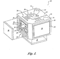
- FIG. 1 is an exploded pictorial view of a 3-axis or "triaxial" MEMS inertial sensor device having individual MEMS inertial sensors mounted on the 3-dimensional package of the invention embodied as a stable, structurally-sound generally cubical mechanical mounting base. Accordingly, a 3-axis MEMS inertial sensor device 10 is provided having three MEMS inertial sensors 12 and complementary electronic circuits 14 (200 MOhm major signal conditioning resistors shown) mounted on the 3-dimensional package 16 of the invention.
- the 3-dimensional package 16 of the invention is embodied as a miniature generally cubicle block having a package interface surface 18 and one or more MEMS sensor mounting surfaces 20, 22, 24
- Each of the sensor mounting surfaces 20, 22 is structured mutually orthogonal to and contiguous with the package interface surface 18, and the sensor mounting surface 24 is structured mutually parallel to and spaced away from the package interface surface 18.
- One, two or three of the MEMS sensors 12 are mounted directly to the 3-dimensional package 16 ofthe invention using well-known conventional die-bonding techniques suited for MEMS sensors
- the device package 16 further provides integral metalization of signal and power traces to electrical bonding pads for direct bonding of the MEMS inertial sensor triad device 10 to a next level assembly with the host structure.
- the device package 16 is further embodied having means for routing electrical power, ground and operational signals between the orthogonal and parallel sensor mounting surfaces 20, 22, 24 and the common interface surface 18, as illustrated, or another suitable surface
- a quantity of die bond pads 25 are provided on a die bond shelf 27 structured above and surrounding each MEMS sensor mounting surfaces 20. 22. 24
- a quantity of electrical traces are routed over the surfaces 18, 20, 22, 24 or through the body of the package 16 to a quantity of electrical interface contacts, or "pad outs,” 26 that may be grouped, as illustrated, as a function the sensor mounting surface 20, 22, 24 with which the electrical contacts 26 communicate
- each of the sensor mounting surfaces 20, 22, 24 is optionally structured as the floor of a recess or cavity in the body of the package 16, as illustrated, wherein the MEMS inertial sensors 12 and complementary electronic circuits 14 are mounted. Accordingly, individual covers or lids 28 may be provided over the sensors 12 and circuits 14 and bonded, adhesively or otherwise, to the outer surfaces of the package body 16. The covers 28 thereby protect the sensitive components.
- the mounting area of the MEMS sensors 12 includes provision for hermetically sealing the devices within the 3-dimensionally-structured sensor mounting cavities 20, 22, 24. For example, a portion 32 of the outer surfaces of the package body 16 surrounding each of the sensor mounting surfaces 20. 22, 24 is prepared by conventional means for hermetically sealing for attaching and hermetically sealing the covers 28. Hermetic sealing of the sensors 12 is provided using solder or laser attachment of metalized lids 28, or hermetic epoxy sealing of the lids 28, to the prepared surfaces 32
- the package interface surface 18 is structured for mechanically mounting the package 16 to a host structure (not shown) that is to be monitored.
- the package interface surface 18 includes a structural key 30 for interfacing with a cooperating key mechanism provided on the host structure for rotationally orienting the device package 16 relative to the host structure
- the invention provides the unique miniature MEMS inertial triad 10 of orthogoanally mounted sensors This embodiment, and alternative embodiments discussed herein, permits the MEMS inertial triad 10 to be manually manipulated for calibration and test, or for attachment to the host structure for calibration and test at the next level of assembly.
- the package 16 is alternatively embodied having means for mechanically securing it to the host structure.
- the MEMS inertial sensor device 10 of the invention when the MEMS inertial sensor device 10 of the invention is embodied as a two-axis or "biaxial" MEMS inertial sensor having the MEMS sensors 12 mounted on the two sensor mounting surfaces 20, 22 orthogonal to and contiguous with the package interface surface 18, a bolt hole 32 through the body of the package 16, or another suitable mechanical securing means, is provided for mechanical securing the package 16 to the host structure
- FIG 2 shows the triaxial MEMS inertial sensor device 10 rotated so that the three sensor mounting surfaces 20, 22, 24 are observed Two of the sensors 12 being protected by hermetically sealed covers 28, and the third sensor 12 being removed so that sensor mounting surface 20 is visible.
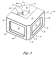
- Figure 3 illustrates the mechanical mounting base of the invention embodied as the generally cubicle 3-dimensional package 16 structure formed in a ceramic substrate
- the choice of ceramic ensures that the package 16 is structurally sound and is closely thermally matched to the substrate material on which the MEMS sensors 12 are fabricated
- the ceramic package 16 is configured using conventional ceramic fabrication techniques.
- the 3-dimensional package 16 is machined from a solid ceramic such as MACOR ® a machinable ceramic commercially available from Corning Incorporated.
- the 3-dimensional package 16 is molded of a moldable ceramic, or built-up using conventional HTCC (high temperature ceramic co-firing) or LTCC (low temperature ceramic co-firing) techniques.
- the fabrication technique is selected as a function of specifics of the package design and particular embodiment, which are determined as a function of the MEMS sensors incorporated in the device 10, LTCC and HTCC co-fired techniques permit metalization of the electrical power and signal traces during fabrication Alternatively, metalization ofthe electrical power and signal traces can be implemented using thin film deposition or thick film printing techniques.
- the ceramic package 16 is fabricated having the plurality of substantially mutually orthogonal and parallel surfaces 18, 20, 22, 24, the surfaces 20, 22, 24 each being large enough and appropriately structured for mechanically mounting a single MEMS sensor 12 and, optionally, the related electronic circuits 14.
- the ceramic package 16 is provided with cover mounting surfaces 34. 36, 38 completely surrounding and spaced above the recessed sensor mounting surfaces 20, 22, 24.
- the MEMS sensor surfaces 20, 22, 24 are spaced sufficiently below the respective surrounding surfaces 34, 36, 38 to permit the covers 28 to be engaged with the respective cover mounting surfaces 34, 36. 38 without interfering with the MEMS sensors 12 or electronic circuits 14
- the cover mounting surfaces are sufficiently planar to permit hermetic sealing of the covers 28 and are prepared by conventional means for hermetic sealing of the covers 28, as discussed herein
- the ceramic package 16 incorporates structural features for keying the MEMS sensor triad 10 in alignment and rotational orientation with the host structure both for optimizing performance and for easing assembly
- the package interface surface 18 includes the structural key 30 for embodied by example and without limitation as one or more substantially rectangular blocks 40, 42 having a combined length structured to ensure adequate rotational orientation relative to the host structure when mated with a cooperating keyway therein.
- the structural key 30 is oriented relative to the MEMS sensor mounting surfaces 20, 22 orthogonal to the package interface surface 18 to optimize orientation to the host structure.
- the structural key 30 is rotated diagonally to the interface surface 18, i e. at about 45 degrees from each of the orthogonal sensor mounting surfaces 20, 22.
- the package interface surface 18 is optionally embodied as an offset surface relative to a relieved surface portion 44 whereupon the electrical interface contacts 26 may be provided, as discussed below Interference with a flush surface-to-surface interface is thereby avoided.
- the means for mechanically securing the ceramic package 16 to the host structure is provided in balanced alignment with the cubicle ceramic package 16.
- the mechanical securing means embodied as bolt hole 32 passes through the geometric center of the cubic structure between the package interface surface 18 and the opposite package surface 24. Such alignment tends to stabilize the ceramic package 16 relative to the host structure when secured by a fastener (not shown) through the bolt hole 32 into a threaded receiver in the mating surface of the host structure
- unused volume of the ceramic package 16 is eliminated by beveled corners 46, 48 that also assist with mounting on the host structure by providing clearances for machined surfaces such as internal radii. Beveled corners 46. 48 may also provide clearance for a wiring harness within the host structure. Other edge surfaces 50 of the cubicle ceramic package 16 are also beveled or otherwise relieved to accommodate internal radii that may be present in the host structure due to the inherent limitations of machining and other manufacturing processes.
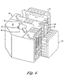
- FIG 4 illustrates the MEMS inertial sensor device 10 of the invention embodied as an alternative biaxial to or two-axis sensor device having individually hermetically packaged MEMS inertial sensors 52.
- the cubicle ceramic package 16 ofthe invention is alternatively embodied to include provisions for mounting the individually hermetically packaged MEMS sensors 52 onto its 3-D structure
- the MEMS devices 52 are for example individually hermetically packaged in ceramic chip carriers of an appropriate configuration
- the MEMS devices 52 are configured in a well-known 20-pin LCC (leaded chip carrier).
- the sensor mounting surfaces 20, 22 orthogonal to and contiguous with the interface surface 18 are structured to accommodate the LCC packages containing the MEMS devices
- the recessed sensor mounting surfaces 20, 22 are open to the common interface surface 18 to accommodate the LCC packages.
- the LCC packages are individually hermetically sealed, accommodations need not be made for attaching and hermetically sealing independent device covers 28. as described in Figures 1 and 2. Electrical power, ground and operational signal lines are brought to the interface contacts 26 over external surfaces of the package 16. as illustrated.
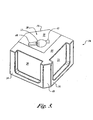
- Figure 5 illustrates the cubicle ceramic package 16 of the invention embodied to accommodate the MEMS sensors 52 embodied in LCC packages, as shown in Figure 4. Accordingly, as embodied in Figure 5, the recessed sensor mounting surfaces 20, 22 are open on the edge contiguous with the relieved portion 44 of the package interface surface 18. The package 16 thereby accommodates the external routing of the electrical power, ground and signal lines without interference.
- Figure 6 illustrates an alternative embodiment ofthe 3-dimensional package 16 shown in Figure 5 wherein a quantity of recesses 54 are provided in the relevant surfaces of the package 16 for routing the electrical lines below the package body surface, as shown in Figure 4.
- the electrical lines are thereby protected from damage that might otherwise interrupt communications with the assembled MEMS devices 52.
Abstract
Description
- The present invention relates to packaging of sensor devices and methods, and in particular to 3-dimensional structures for packaging of Micro Electro-Mechanical System (MEMS) sensor devices
- Micro Electro-Mechanical System (MEMS) inertial sensors, including accelerometers, gyroscopes and magnetometers, are generally well-known and commercially available from Honeywell International, Incorporated, the assignee of the present patent application These MEMS inertial sensors are typically mounted as individual units directly on the host structure to be monitored. While effective, such direct mounting places increased demands on the precision and accuracy with which the structure to be monitored is manufactured in order to achieve true three-axis orientation. Nor can direct mounting on the host structure obtain the small size advantages offered by the MEMS sensors. Furthermore, assembly and testing of the MEMS sensors requires access to and manipulation of the entire host structure. These limitations in turn limit the performance that can be achieved by the MEMS sensors
- US 6 123 107 discloses an apparatus for mounting micromechanical fluid control components includes a manifold interface plate adaptable for connection to a manifold substrate oriented in a horizontal plane. The manifold interface plate receives mounting stress forces from the manifold substrate along the horizontal plane. An orthogonal component plate is connected to the manifold interface plate in a vertical plane with respect to the horizontal plane of the manifold substrate. The orthogonal component plate includes an orthogonal mounting surface with a micromechanical fluid control component mounted on it. The position of the micromechanical fluid control component on the orthogonal mounting surface substantially isolates the micromechanical fluid control component from the mounting stress forces.
- The invention provides an apparatus as defined by claim 1.
- The apparatus may include the features of any one or more of dependent claims 2 to 6.
- The present invention is a miniature 3-dimensional packaging structure for mounting one or more Micro Electro-Mechanical System (MEMS) inertial sensors that captures the small size advantage of MEMS sensors and overcomes limitations ofthe prior art by providing a stable, structurally sound base for mechanically mounting the MEMS sensors. The package provides a means for transferring electrical power and operating signals to:and from the MEMS sensors. The package also provides means for insuring maximum performance is obtained over dynamic environments observed by the MEMS inertial sensors.
- The 3-dimension package structure of the invention accepts one, two or three MEMS inertial sensors in close-proximity orthogonal positions. The structural ceramic package provides mounting for each axis of a three-axis MEMS inertial sensor triad on orthogonal sides of a generally cubical package that provides a structurally sound base for rugged mounting ofthe MEMS inertial sensors. These MEMS sensors are alternatively separately packaged in chip carrier devices, such as a ceramic 20-pin leaded chip carrier (LCC), and are attached to the 3-dimension package structure of the invention. According to one embodiment of the invention, the 3-dimension package structure of the invention provides direct mounting of the MEMS sensors by conventional die bonding techniques
- Accordingly- one embodiment of the invention provides an apparatus for mechanically mounting one or more MEMS sensors on a stable, structurally sound base, the base being a generally cubical block formed in a substrate having a plurality of substantially planar and mutually orthogonal surfaces, wherein a first one of the surfaces is structured for rotationally interfacing with a host structure that is to be monitored; a second one of the surfaces is structured for mechanically mounting of a MEMS sensor, and a plurality of electrical signal carriers communicate between the MEMS sensor mounting surface and a plurality of electrical interface contacts positioned on the interfacing surface
- According to one aspect of the invention, the substrate is a ceramic substrate.
- According to another aspect of the invention, the first surface structured for rotationally interfacing with a host structure includes a structural key oriented diagonally to the surface
- According to another aspect of the invention, the generally cubical block includes a generally cylindrical aperture communicating between the interfacing surface and a surface of the block opposite thereto
- According to another aspect of the invention, the generally cubical block further includes multiple surfaces structured for mechanically mounting of a MEMS sensor, a quantity of the electrical signal carriers communicate between each of the MEMS sensor mounting surfaces and corresponding electrical interface contacts positioned on the interfacing surface: and a MEMS sensor is mounted to each of the MEMS sensor mounting surfaces and is electrically interfaced to the electrical signal carriers.
- According to another aspect of the invention, each of the MEMS sensors is a MEMS sensor packaged in a hermetically sealed LCC.
- According to another aspect of the invention, each of the plurality of surfaces structured for mechanically mounting of a MEMS sensor includes a recessed cavity formed in and peripherally surrounded by a surface of the block, and a cover is installed over each MEMS sensor and sealed to the surface of the block. According to another aspect of the invention, the seals between each of the covers and the block is a hermetic seal
- The foregoing aspects and many of the attendant advantages of this invention win become more readily appreciated as the same becomes better understood by reference to the following detailed description, when taken in conjunction with the accompanying drawings, wherein.
- Figure 1 is an exploded pictorial view of a 3-axis MEMS inertial sensor device mounted on the stable, structurally-sound mechanical mounting base of the invention embodied as a generally cubical 3-dimensional package that provides for mounting on orthogonal sides thereof each axis of a 3-axis MEMS inertial sensor wherein the MEMS sensors are hermetically sealed with individual covers;
- Figure 2 shows the triaxial MEMS inertial sensor device rotated with the three device mounting surfaces shown, two of the sensors being protected by hermetically sealed covers and the third sensor being removed so that the device mounting surface is shown.
- Figure 3 illustrates the mechanical mounting base of the invention embodied as a structurally sound generally cubicle 3-dimensional package structure formed in a ceramic substrate that is thermally matched to the substrates in which the MEMS inertial sensors are fabricated;
- Figure 4 illustrates the MEMS inertial sensor device of the invention embodied as an alternative biaxial or two-axis sensor device having individually hermetically packaged MEMS sensors;
- Figure 5 illustrates the cubicle ceramic package of the invention embodied to accommodate the MEMS sensors embodied in LCC packages, as shown in Figure 4, and
- Figure 6 illustrates an alternative embodiment of the 3-dimensional package shown in Figure 5 wherein one or more recesses are provided in the relevant surfaces of the package for routing the electrical lines below the surface of the package body, as shown in Figure 4.
- In the Figures, like numerals indicate like elements
- The present invention is an apparatus and method for mechanically mounting one or more Micro Electro-Mechanical System (MEMS) sensors on a stable, structurally sound base that is formed of a miniature generally cubical ceramic block having two or more substantially orthogonal surfaces. One of the two orthogonal surfaces is structured for mechanically mounting of a single MEMS sensors. Means are provided for routing power, ground and signals between each of the one or more MEMS sensors and a common surface of the mounting block for interface with external circuitry. One of the orthogonal surfaces, for example the common surface hosting the external circuitry interface, includes a structural key for rotationally interfacing with an external key mechanism in the host structure to be monitored. Means are provided for mechanically securing to the host structure. Additionally, means may be provided for hermetically sealing each of the one or more MEMS sensor devices.
- Figure 1 is an exploded pictorial view of a 3-axis or "triaxial" MEMS inertial sensor device having individual MEMS inertial sensors mounted on the 3-dimensional package of the invention embodied as a stable, structurally-sound generally cubical mechanical mounting base. Accordingly, a 3-axis MEMS
inertial sensor device 10 is provided having three MEMS inertial sensors 12 and complementary electronic circuits 14 (200 MOhm major signal conditioning resistors shown) mounted on the 3-dimensional package 16 of the invention. - As is more fully discussed below, the 3-
dimensional package 16 of the invention is embodied as a miniature generally cubicle block having apackage interface surface 18 and one or more MEMSsensor mounting surfaces sensor mounting surfaces package interface surface 18, and thesensor mounting surface 24 is structured mutually parallel to and spaced away from thepackage interface surface 18. One, two or three of the MEMS sensors 12 are mounted directly to the 3-dimensional package 16 ofthe invention using well-known conventional die-bonding techniques suited for MEMS sensors - Signal and power routing to the MEMS sensors 12 is accomplished via conventional wire bonding techniques, ribbon welding, or flip-chip attach methods According to one embodiment of the invention, the
device package 16 further provides integral metalization of signal and power traces to electrical bonding pads for direct bonding of the MEMS inertialsensor triad device 10 to a next level assembly with the host structure. - The
device package 16 is further embodied having means for routing electrical power, ground and operational signals between the orthogonal and parallelsensor mounting surfaces common interface surface 18, as illustrated, or another suitable surface For example, a quantity of diebond pads 25 are provided on adie bond shelf 27 structured above and surrounding each MEMSsensor mounting surfaces 20. 22. 24 A quantity of electrical traces (more clearly shown in subsequent Figures) are routed over thesurfaces package 16 to a quantity of electrical interface contacts, or "pad outs," 26 that may be grouped, as illustrated, as a function thesensor mounting surface electrical contacts 26 communicate - Each of the
sensor mounting surfaces package 16, as illustrated, wherein the MEMS inertial sensors 12 and complementaryelectronic circuits 14 are mounted. Accordingly, individual covers orlids 28 may be provided over the sensors 12 andcircuits 14 and bonded, adhesively or otherwise, to the outer surfaces of thepackage body 16. Thecovers 28 thereby protect the sensitive components. Furthermore, according to one alternative embodiment of the invention, the mounting area of the MEMS sensors 12 includes provision for hermetically sealing the devices within the 3-dimensionally-structuredsensor mounting cavities portion 32 of the outer surfaces of thepackage body 16 surrounding each of thesensor mounting surfaces 20. 22, 24 is prepared by conventional means for hermetically sealing for attaching and hermetically sealing thecovers 28. Hermetic sealing of the sensors 12 is provided using solder or laser attachment ofmetalized lids 28, or hermetic epoxy sealing of thelids 28, to the preparedsurfaces 32 - The
package interface surface 18 is structured for mechanically mounting thepackage 16 to a host structure (not shown) that is to be monitored. According to one embodiment of the invention, thepackage interface surface 18 includes astructural key 30 for interfacing with a cooperating key mechanism provided on the host structure for rotationally orienting thedevice package 16 relative to the host structure - Once the MEMS sensors 12 are attached to the 3-D structure of the
package 16, the invention provides the unique miniature MEMSinertial triad 10 of orthogoanally mounted sensors This embodiment, and alternative embodiments discussed herein, permits the MEMSinertial triad 10 to be manually manipulated for calibration and test, or for attachment to the host structure for calibration and test at the next level of assembly. - The
package 16 is alternatively embodied having means for mechanically securing it to the host structure. For example, according to one embodiment of the invention, when the MEMSinertial sensor device 10 of the invention is embodied as a two-axis or "biaxial" MEMS inertial sensor having the MEMS sensors 12 mounted on the twosensor mounting surfaces package interface surface 18, abolt hole 32 through the body of thepackage 16, or another suitable mechanical securing means, is provided for mechanical securing thepackage 16 to the host structure - Figure 2 shows the triaxial MEMS
inertial sensor device 10 rotated so that the threesensor mounting surfaces sensor mounting surface 20 is visible. - Figure 3 illustrates the mechanical mounting base of the invention embodied as the generally cubicle 3-
dimensional package 16 structure formed in a ceramic substrate The choice of ceramic ensures that thepackage 16 is structurally sound and is closely thermally matched to the substrate material on which the MEMS sensors 12 are fabricated For example, the ceramic substrate in which thepackage 16 is formed in an alumina ceramic substrate for optimum matching of coefficients of thermal expansion. Theceramic package 16 is configured using conventional ceramic fabrication techniques. For example, the 3-dimensional package 16 is machined from a solid ceramic such as MACOR® a machinable ceramic commercially available from Corning Incorporated. Alternatively, the 3-dimensional package 16 is molded of a moldable ceramic, or built-up using conventional HTCC (high temperature ceramic co-firing) or LTCC (low temperature ceramic co-firing) techniques. The fabrication technique is selected as a function of specifics of the package design and particular embodiment, which are determined as a function of the MEMS sensors incorporated in thedevice 10, LTCC and HTCC co-fired techniques permit metalization of the electrical power and signal traces during fabrication Alternatively, metalization ofthe electrical power and signal traces can be implemented using thin film deposition or thick film printing techniques. - The
ceramic package 16 is fabricated having the plurality of substantially mutually orthogonal andparallel surfaces surfaces electronic circuits 14. According to one embodiment of the invention, theceramic package 16 is provided with cover mounting surfaces 34. 36, 38 completely surrounding and spaced above the recessedsensor mounting surfaces surfaces covers 28 to be engaged with the respectivecover mounting surfaces electronic circuits 14 The cover mounting surfaces are sufficiently planar to permit hermetic sealing of thecovers 28 and are prepared by conventional means for hermetic sealing of thecovers 28, as discussed herein - According to one embodiment of the invention, the
ceramic package 16 incorporates structural features for keying theMEMS sensor triad 10 in alignment and rotational orientation with the host structure both for optimizing performance and for easing assembly For example, thepackage interface surface 18 includes thestructural key 30 for embodied by example and without limitation as one or more substantiallyrectangular blocks structural key 30 is oriented relative to the MEMSsensor mounting surfaces package interface surface 18 to optimize orientation to the host structure. For example, thestructural key 30 is rotated diagonally to theinterface surface 18, i e. at about 45 degrees from each of the orthogonalsensor mounting surfaces - The
package interface surface 18 is optionally embodied as an offset surface relative to arelieved surface portion 44 whereupon theelectrical interface contacts 26 may be provided, as discussed below Interference with a flush surface-to-surface interface is thereby avoided. - The means for mechanically securing the
ceramic package 16 to the host structure, such asbolt hole 32 or another suitable mechanical securing means, is provided in balanced alignment with the cubicleceramic package 16. For example, the mechanical securing means embodied asbolt hole 32 passes through the geometric center of the cubic structure between thepackage interface surface 18 and theopposite package surface 24. Such alignment tends to stabilize theceramic package 16 relative to the host structure when secured by a fastener (not shown) through thebolt hole 32 into a threaded receiver in the mating surface of the host structure - According to one embodiment of the invention, unused volume of the
ceramic package 16 is eliminated bybeveled corners Beveled corners 46. 48 may also provide clearance for a wiring harness within the host structure. Other edge surfaces 50 of the cubicleceramic package 16 are also beveled or otherwise relieved to accommodate internal radii that may be present in the host structure due to the inherent limitations of machining and other manufacturing processes. - Figure 4 illustrates the MEMS
inertial sensor device 10 of the invention embodied as an alternative biaxial to or two-axis sensor device having individually hermetically packaged MEMSinertial sensors 52. Accordingly, the cubicleceramic package 16 ofthe invention is alternatively embodied to include provisions for mounting the individually hermetically packagedMEMS sensors 52 onto its 3-D structure TheMEMS devices 52 are for example individually hermetically packaged in ceramic chip carriers of an appropriate configuration According to one embodiment ofthe invention, theMEMS devices 52 are configured in a well-known 20-pin LCC (leaded chip carrier). The embodiment illustrated in Figure 4 accordingly permits "known good die" (KGD) to be mounted to theceramic package 16 This embodiment also permits theMEMS sensors 52 to be reworked as individual entities In operation, KGD are tested or calibrated prior to installation onto the 3-D ceramic package 16. Signal and power routing are incorporated into these alternative embodiments - The sensor mounting surfaces 20, 22 orthogonal to and contiguous with the
interface surface 18 are structured to accommodate the LCC packages containing the MEMS devices For example, the recessedsensor mounting surfaces common interface surface 18 to accommodate the LCC packages. Because the LCC packages are individually hermetically sealed, accommodations need not be made for attaching and hermetically sealing independent device covers 28. as described in Figures 1 and 2. Electrical power, ground and operational signal lines are brought to theinterface contacts 26 over external surfaces of thepackage 16. as illustrated. - Figure 5 illustrates the cubicle
ceramic package 16 of the invention embodied to accommodate theMEMS sensors 52 embodied in LCC packages, as shown in Figure 4. Accordingly, as embodied in Figure 5, the recessedsensor mounting surfaces relieved portion 44 of thepackage interface surface 18. Thepackage 16 thereby accommodates the external routing of the electrical power, ground and signal lines without interference. - Figure 6 illustrates an alternative embodiment ofthe 3-
dimensional package 16 shown in Figure 5 wherein a quantity ofrecesses 54 are provided in the relevant surfaces of thepackage 16 for routing the electrical lines below the package body surface, as shown in Figure 4. The electrical lines are thereby protected from damage that might otherwise interrupt communications with the assembledMEMS devices 52.
Claims (6)
- An apparatus for mounting one or more Micro Electro-Mechanical System (MEMS) sensors, the apparatus comprising:means for orthogonally orienting each of one or more MEMS sensor mounting surfaces relative to a common interface surface,means for routing electrical power, ground and operational signals between each sensor mounting surfaces and the common interface surface; andmeans for rotationally interfacing the common interface surface with an external key mechanism.
- The mounting apparatus of claim 1, further comprising means for mechanically securing the common interface surface to a host structure that is to be monitored
- The mounting apparatus of claim 1, further comprising a MEMS sensor mounted on one or more ofthe sensor mounting surfaces, each of the MEMS sensors being electrically coupled to the means for routing electrical power, ground and operational signals
- The mounting apparatus of claim 3, further comprising means for hermetically sealing each of the one or more MEMS sensors.
- The mounting apparatus of claim 1 wherein the means for orthogonally orienting each of one or more MEMS sensor mounting surfaces relative to a common interface surface further comprises means for mounting each of the one or more MEMS sensors below a structural surface of a generally cubical ceramic mounting block.
- The mounting apparatus of claim 5, further comprising means for hermetically sealing each of the one or more MEMS sensors
Applications Claiming Priority (2)
| Application Number | Priority Date | Filing Date | Title |
|---|---|---|---|
| US10/377,439 US6918297B2 (en) | 2003-02-28 | 2003-02-28 | Miniature 3-dimensional package for MEMS sensors |
| PCT/US2004/006207 WO2004079874A1 (en) | 2003-02-28 | 2004-02-27 | Miniature 3-dimensional package for mems sensors |
Publications (2)
| Publication Number | Publication Date |
|---|---|
| EP1642365A1 EP1642365A1 (en) | 2006-04-05 |
| EP1642365B1 true EP1642365B1 (en) | 2007-05-02 |
Family
ID=32908142
Family Applications (1)
| Application Number | Title | Priority Date | Filing Date |
|---|---|---|---|
| EP04715806A Expired - Lifetime EP1642365B1 (en) | 2003-02-28 | 2004-02-27 | Miniature 3-dimensional package for mems sensors |
Country Status (5)
| Country | Link |
|---|---|
| US (1) | US6918297B2 (en) |
| EP (1) | EP1642365B1 (en) |
| AT (1) | ATE361563T1 (en) |
| DE (1) | DE602004006270T2 (en) |
| WO (1) | WO2004079874A1 (en) |
Cited By (2)
| Publication number | Priority date | Publication date | Assignee | Title |
|---|---|---|---|---|
| US9213046B2 (en) | 2010-08-09 | 2015-12-15 | SZ DJI Technology Co., Ltd. | Micro inertial measurement system |
| US9664516B2 (en) | 2014-04-25 | 2017-05-30 | SZ DJI Technology Co., Ltd. | Inertial sensing device |
Families Citing this family (63)
| Publication number | Priority date | Publication date | Assignee | Title |
|---|---|---|---|---|
| US7040922B2 (en) * | 2003-06-05 | 2006-05-09 | Analog Devices, Inc. | Multi-surface mounting member and electronic device |
| US7458263B2 (en) * | 2003-10-20 | 2008-12-02 | Invensense Inc. | Method of making an X-Y axis dual-mass tuning fork gyroscope with vertically integrated electronics and wafer-scale hermetic packaging |
| US7370530B2 (en) * | 2004-09-01 | 2008-05-13 | Honeywell International Inc. | Package for MEMS devices |
| US7442570B2 (en) | 2005-03-18 | 2008-10-28 | Invensence Inc. | Method of fabrication of a AL/GE bonding in a wafer packaging environment and a product produced therefrom |
| US7246524B1 (en) * | 2005-05-02 | 2007-07-24 | Sandia Corporation | MEMS fluidic actuator |
| KR100655218B1 (en) * | 2005-07-01 | 2006-12-08 | 삼성전자주식회사 | Three dimensional semiconductor module having multilateral-type ground block |
| JP2007040766A (en) * | 2005-08-01 | 2007-02-15 | Toyota Motor Corp | Sensor unit |
| US7919717B2 (en) | 2005-08-19 | 2011-04-05 | Honeywell International Inc. | Three-dimensional printed circuit board |
| JP2007127607A (en) * | 2005-11-07 | 2007-05-24 | Mitsutoyo Corp | Sensor block |
| US7467552B2 (en) * | 2005-11-10 | 2008-12-23 | Honeywell International Inc. | Miniature package for translation of sensor sense axis |
| US7621183B2 (en) * | 2005-11-18 | 2009-11-24 | Invensense Inc. | X-Y axis dual-mass tuning fork gyroscope with vertically integrated electronics and wafer-scale hermetic packaging |
| US7518493B2 (en) * | 2005-12-01 | 2009-04-14 | Lv Sensors, Inc. | Integrated tire pressure sensor system |
| US7468556B2 (en) * | 2006-06-19 | 2008-12-23 | Lv Sensors, Inc. | Packaging of hybrid integrated circuits |
| US7968807B2 (en) | 2006-07-21 | 2011-06-28 | Analog Devices, Inc. | Package having a plurality of mounting orientations |
| US8047075B2 (en) | 2007-06-21 | 2011-11-01 | Invensense, Inc. | Vertically integrated 3-axis MEMS accelerometer with electronics |
| US8462109B2 (en) | 2007-01-05 | 2013-06-11 | Invensense, Inc. | Controlling and accessing content using motion processing on mobile devices |
| US7934423B2 (en) | 2007-12-10 | 2011-05-03 | Invensense, Inc. | Vertically integrated 3-axis MEMS angular accelerometer with integrated electronics |
| US8141424B2 (en) | 2008-09-12 | 2012-03-27 | Invensense, Inc. | Low inertia frame for detecting coriolis acceleration |
| US8250921B2 (en) | 2007-07-06 | 2012-08-28 | Invensense, Inc. | Integrated motion processing unit (MPU) with MEMS inertial sensing and embedded digital electronics |
| US7796872B2 (en) * | 2007-01-05 | 2010-09-14 | Invensense, Inc. | Method and apparatus for producing a sharp image from a handheld device containing a gyroscope |
| US20090262074A1 (en) * | 2007-01-05 | 2009-10-22 | Invensense Inc. | Controlling and accessing content using motion processing on mobile devices |
| US8952832B2 (en) | 2008-01-18 | 2015-02-10 | Invensense, Inc. | Interfacing application programs and motion sensors of a device |
| US8020441B2 (en) | 2008-02-05 | 2011-09-20 | Invensense, Inc. | Dual mode sensing for vibratory gyroscope |
| US8508039B1 (en) | 2008-05-08 | 2013-08-13 | Invensense, Inc. | Wafer scale chip scale packaging of vertically integrated MEMS sensors with electronics |
| US7790502B2 (en) * | 2007-12-10 | 2010-09-07 | Honeywell International Inc. | Method of manufacturing flexible semiconductor assemblies |
| US8100010B2 (en) * | 2008-04-14 | 2012-01-24 | Honeywell International Inc. | Method and system for forming an electronic assembly having inertial sensors mounted thereto |
| DE102008021584A1 (en) * | 2008-04-30 | 2009-11-05 | Continental Automotive Gmbh | Device for use in sensor unit for arranging sensor on printed circuit board, comprises flat base section and holding device which is arranged on base section which is formed for mounting sensor printed circuit board carrying sensor |
| US8072379B2 (en) * | 2008-05-12 | 2011-12-06 | Qualcomm Incorporated | GPS power savings using low power sensors |
| DE102009001247A1 (en) | 2009-02-27 | 2010-09-09 | Sensordynamics Ag | Micro-electro-mechanical sensor |
| US9097524B2 (en) | 2009-09-11 | 2015-08-04 | Invensense, Inc. | MEMS device with improved spring system |
| US8534127B2 (en) | 2009-09-11 | 2013-09-17 | Invensense, Inc. | Extension-mode angular velocity sensor |
| DE102010000848A1 (en) * | 2010-01-13 | 2011-07-14 | Robert Bosch GmbH, 70469 | Carrier material with a mechanical filter characteristic and method for producing a carrier material |
| US8692366B2 (en) | 2010-09-30 | 2014-04-08 | Analog Device, Inc. | Apparatus and method for microelectromechanical systems device packaging |
| US8567246B2 (en) | 2010-10-12 | 2013-10-29 | Invensense, Inc. | Integrated MEMS device and method of use |
| US8947081B2 (en) | 2011-01-11 | 2015-02-03 | Invensense, Inc. | Micromachined resonant magnetic field sensors |
| US8860409B2 (en) | 2011-01-11 | 2014-10-14 | Invensense, Inc. | Micromachined resonant magnetic field sensors |
| US9664750B2 (en) | 2011-01-11 | 2017-05-30 | Invensense, Inc. | In-plane sensing Lorentz force magnetometer |
| TW201245724A (en) * | 2011-01-25 | 2012-11-16 | Epcos Ag | Sensor arrangement |
| US8459112B2 (en) * | 2011-06-09 | 2013-06-11 | Honeywell International Inc. | Systems and methods for three dimensional sensors |
| US8901432B2 (en) | 2011-09-30 | 2014-12-02 | Honeywell International Inc. | Mitigation of block bending in a ring laser gyroscope caused by thermal expansion or compression of a circuit board |
| US8905635B2 (en) | 2011-09-30 | 2014-12-09 | Honeywell International Inc. | Temperature sensor attachment facilitating thermal conductivity to a measurement point and insulation from a surrounding environment |
| US8836132B2 (en) | 2012-04-03 | 2014-09-16 | Analog Devices, Inc. | Vertical mount package and wafer level packaging therefor |
| US9155198B2 (en) * | 2012-05-17 | 2015-10-06 | Eagantu Ltd. | Electronic module allowing fine tuning after assembly |
| JP2014048090A (en) * | 2012-08-30 | 2014-03-17 | Seiko Epson Corp | Electronic module, electronic apparatus, and movable body |
| US9475694B2 (en) | 2013-01-14 | 2016-10-25 | Analog Devices Global | Two-axis vertical mount package assembly |
| JP6331266B2 (en) * | 2013-05-24 | 2018-05-30 | セイコーエプソン株式会社 | Sensor unit, electronic device and moving body |
| US9235937B1 (en) | 2013-06-05 | 2016-01-12 | Analog Devices, Inc. | Mounting method for satellite crash sensors |
| US9549464B2 (en) * | 2013-08-30 | 2017-01-17 | Apple Inc. | Modules for increasing useable space on circuit boards |
| EP3257074A1 (en) | 2015-02-11 | 2017-12-20 | InvenSense, Inc. | 3D INTEGRATION USING Al-Ge EUTECTIC BOND INTERCONNECT |
| FI127202B (en) * | 2015-04-16 | 2018-01-31 | Murata Manufacturing Co | Triaxate gyroscope |
| US10663186B2 (en) * | 2016-05-31 | 2020-05-26 | Robert J. Mowris | Apparatus and methods to determine economizer faults |
| CN105910635B (en) * | 2016-06-23 | 2019-04-26 | 北京合众思壮科技股份有限公司 | A kind of Inertial Measurement Unit mounting body |
| US11647678B2 (en) | 2016-08-23 | 2023-05-09 | Analog Devices International Unlimited Company | Compact integrated device packages |
| US10192850B1 (en) | 2016-09-19 | 2019-01-29 | Sitime Corporation | Bonding process with inhibited oxide formation |
| US10472098B2 (en) | 2016-10-25 | 2019-11-12 | Honeywell International Inc. | Mass efficient reaction wheel assembly systems including multi-faceted bracket structures |
| US10629574B2 (en) | 2016-10-27 | 2020-04-21 | Analog Devices, Inc. | Compact integrated device packages |
| US10697800B2 (en) | 2016-11-04 | 2020-06-30 | Analog Devices Global | Multi-dimensional measurement using magnetic sensors and related systems, methods, and integrated circuits |
| JP6819338B2 (en) * | 2017-02-13 | 2021-01-27 | セイコーエプソン株式会社 | Physical quantity detector and electronic equipment |
| CN107285274B (en) * | 2017-05-10 | 2019-03-01 | 中国航空工业集团公司西安飞行自动控制研究所 | A kind of three-dimension packaging method of micromachined process |
| EP3795076B1 (en) | 2018-01-31 | 2023-07-19 | Analog Devices, Inc. | Electronic devices |
| GB2571916A (en) * | 2018-02-23 | 2019-09-18 | Atlantic Inertial Systems Ltd | Inertial measurement units |
| US10952324B2 (en) * | 2019-04-15 | 2021-03-16 | Facebook Technologies, Llc | Spacer for surface mountable electronic components |
| CN112506098A (en) * | 2020-11-27 | 2021-03-16 | 中电科技集团重庆声光电有限公司 | LTCC-based monolithic unmanned aerial vehicle integrated navigation flight control micro system |
Family Cites Families (7)
| Publication number | Priority date | Publication date | Assignee | Title |
|---|---|---|---|---|
| US5434559A (en) * | 1994-07-11 | 1995-07-18 | Smiley; Al W. | Anti-theft alarm and method for protecting movable articles |
| US5756895A (en) * | 1995-09-01 | 1998-05-26 | Hughes Aircraft Company | Tunneling-based rate gyros with simple drive and sense axis coupling |
| US5738548A (en) * | 1996-09-16 | 1998-04-14 | Rutulante; Philip M. | Wall mounted receptacle with retractable extension cord |
| US6123107A (en) * | 1999-07-09 | 2000-09-26 | Redwood Microsystems, Inc. | Apparatus and method for mounting micromechanical fluid control components |
| US6404204B1 (en) * | 2000-05-01 | 2002-06-11 | ARETé ASSOCIATES | Sensor and sensor system for liquid conductivity, temperature and depth |
| US7253079B2 (en) * | 2002-05-09 | 2007-08-07 | The Charles Stark Draper Laboratory, Inc. | Coplanar mounting member for a MEM sensor |
| US6922118B2 (en) * | 2002-11-01 | 2005-07-26 | Hrl Laboratories, Llc | Micro electrical mechanical system (MEMS) tuning using focused ion beams |
-
2003
- 2003-02-28 US US10/377,439 patent/US6918297B2/en not_active Expired - Lifetime
-
2004
- 2004-02-27 DE DE602004006270T patent/DE602004006270T2/en not_active Expired - Lifetime
- 2004-02-27 EP EP04715806A patent/EP1642365B1/en not_active Expired - Lifetime
- 2004-02-27 WO PCT/US2004/006207 patent/WO2004079874A1/en active IP Right Grant
- 2004-02-27 AT AT04715806T patent/ATE361563T1/en not_active IP Right Cessation
Cited By (7)
| Publication number | Priority date | Publication date | Assignee | Title |
|---|---|---|---|---|
| US9213046B2 (en) | 2010-08-09 | 2015-12-15 | SZ DJI Technology Co., Ltd. | Micro inertial measurement system |
| US10132827B2 (en) | 2010-08-09 | 2018-11-20 | SZ DJI Technology Co., Ltd. | Micro inertial measurement system |
| US10732200B2 (en) | 2010-08-09 | 2020-08-04 | SZ DJI Technology Co., Ltd. | Micro inertial measurement system |
| US11215633B2 (en) | 2010-08-09 | 2022-01-04 | SZ DJI Technology Co., Ltd. | Micro inertial measurement system |
| US9664516B2 (en) | 2014-04-25 | 2017-05-30 | SZ DJI Technology Co., Ltd. | Inertial sensing device |
| US10184795B2 (en) | 2014-04-25 | 2019-01-22 | SZ DJI Technology Co., Ltd. | Inertial sensing device |
| US10563985B2 (en) | 2014-04-25 | 2020-02-18 | SZ DJI Technology Co., Ltd. | Inertial sensing device |
Also Published As
| Publication number | Publication date |
|---|---|
| EP1642365A1 (en) | 2006-04-05 |
| ATE361563T1 (en) | 2007-05-15 |
| US6918297B2 (en) | 2005-07-19 |
| WO2004079874A1 (en) | 2004-09-16 |
| DE602004006270T2 (en) | 2008-01-03 |
| DE602004006270D1 (en) | 2007-06-14 |
| US20040169244A1 (en) | 2004-09-02 |
Similar Documents
| Publication | Publication Date | Title |
|---|---|---|
| EP1642365B1 (en) | Miniature 3-dimensional package for mems sensors | |
| EP1785392B1 (en) | Miniature package for translation of sensor sense axis | |
| US7040922B2 (en) | Multi-surface mounting member and electronic device | |
| US5433110A (en) | Detector having selectable multiple axes of sensitivity | |
| US6891239B2 (en) | Integrated sensor and electronics package | |
| US5610431A (en) | Covers for micromechanical sensors and other semiconductor devices | |
| US7238999B2 (en) | High performance MEMS packaging architecture | |
| PL209935B1 (en) | Silicon−based sensor system | |
| EP3403992A1 (en) | Systems and methods for multi-sensor integrated sensor devices | |
| JP2007519902A (en) | A flush proof mass that can be used to detect acceleration along three axes | |
| US11282808B2 (en) | Inertial sensor, electronic instrument, vehicle, and method for manufacturing inertial sensor | |
| US11143669B2 (en) | Inertial measurement units | |
| JP5999908B2 (en) | End-mount sensor | |
| RU2263282C1 (en) | Micro-mechanical sensitive elements-based universal navigation device for controlling motion and unified integrated platform-free inertial navigation system for the device | |
| US20230243866A1 (en) | Multi-axis inertial force sensor | |
| US20240035823A1 (en) | Inertial Measurement Device And Method For Manufacturing Inertial Measurement Device | |
| CN111398630B (en) | Inertial sensor, electronic apparatus, and moving object | |
| EP2413146B1 (en) | Systems and methods for mounting inertial sensors | |
| KR20150141417A (en) | Multi-axis sensor | |
| CN115092877A (en) | Low-stress packaging structure and method for MEMS (micro-electromechanical systems) inertial device based on kovar alloy |
Legal Events
| Date | Code | Title | Description |
|---|---|---|---|
| PUAI | Public reference made under article 153(3) epc to a published international application that has entered the european phase |
Free format text: ORIGINAL CODE: 0009012 |
|
| 17P | Request for examination filed |
Effective date: 20060117 |
|
| AK | Designated contracting states |
Kind code of ref document: A1 Designated state(s): AT BE BG CH CY CZ DE DK EE ES FI FR GB GR HU IE IT LI LU MC NL PT RO SE SI SK TR |
|
| DAX | Request for extension of the european patent (deleted) | ||
| GRAP | Despatch of communication of intention to grant a patent |
Free format text: ORIGINAL CODE: EPIDOSNIGR1 |
|
| GRAS | Grant fee paid |
Free format text: ORIGINAL CODE: EPIDOSNIGR3 |
|
| GRAA | (expected) grant |
Free format text: ORIGINAL CODE: 0009210 |
|
| AK | Designated contracting states |
Kind code of ref document: B1 Designated state(s): AT BE BG CH CY CZ DE DK EE ES FI FR GB GR HU IE IT LI LU MC NL PT RO SE SI SK TR |
|
| PG25 | Lapsed in a contracting state [announced via postgrant information from national office to epo] |
Ref country code: LI Free format text: LAPSE BECAUSE OF FAILURE TO SUBMIT A TRANSLATION OF THE DESCRIPTION OR TO PAY THE FEE WITHIN THE PRESCRIBED TIME-LIMIT Effective date: 20070502 Ref country code: FI Free format text: LAPSE BECAUSE OF FAILURE TO SUBMIT A TRANSLATION OF THE DESCRIPTION OR TO PAY THE FEE WITHIN THE PRESCRIBED TIME-LIMIT Effective date: 20070502 Ref country code: CH Free format text: LAPSE BECAUSE OF FAILURE TO SUBMIT A TRANSLATION OF THE DESCRIPTION OR TO PAY THE FEE WITHIN THE PRESCRIBED TIME-LIMIT Effective date: 20070502 |
|
| REG | Reference to a national code |
Ref country code: GB Ref legal event code: FG4D |
|
| REG | Reference to a national code |
Ref country code: CH Ref legal event code: EP |
|
| REG | Reference to a national code |
Ref country code: IE Ref legal event code: FG4D |
|
| REF | Corresponds to: |
Ref document number: 602004006270 Country of ref document: DE Date of ref document: 20070614 Kind code of ref document: P |
|
| PG25 | Lapsed in a contracting state [announced via postgrant information from national office to epo] |
Ref country code: SE Free format text: LAPSE BECAUSE OF FAILURE TO SUBMIT A TRANSLATION OF THE DESCRIPTION OR TO PAY THE FEE WITHIN THE PRESCRIBED TIME-LIMIT Effective date: 20070802 |
|
| PG25 | Lapsed in a contracting state [announced via postgrant information from national office to epo] |
Ref country code: ES Free format text: LAPSE BECAUSE OF FAILURE TO SUBMIT A TRANSLATION OF THE DESCRIPTION OR TO PAY THE FEE WITHIN THE PRESCRIBED TIME-LIMIT Effective date: 20070813 |
|
| ET | Fr: translation filed | ||
| NLV1 | Nl: lapsed or annulled due to failure to fulfill the requirements of art. 29p and 29m of the patents act | ||
| REG | Reference to a national code |
Ref country code: CH Ref legal event code: PL |
|
| PG25 | Lapsed in a contracting state [announced via postgrant information from national office to epo] |
Ref country code: AT Free format text: LAPSE BECAUSE OF FAILURE TO SUBMIT A TRANSLATION OF THE DESCRIPTION OR TO PAY THE FEE WITHIN THE PRESCRIBED TIME-LIMIT Effective date: 20070502 |
|
| PG25 | Lapsed in a contracting state [announced via postgrant information from national office to epo] |
Ref country code: BE Free format text: LAPSE BECAUSE OF FAILURE TO SUBMIT A TRANSLATION OF THE DESCRIPTION OR TO PAY THE FEE WITHIN THE PRESCRIBED TIME-LIMIT Effective date: 20070502 |
|
| PG25 | Lapsed in a contracting state [announced via postgrant information from national office to epo] |
Ref country code: SI Free format text: LAPSE BECAUSE OF FAILURE TO SUBMIT A TRANSLATION OF THE DESCRIPTION OR TO PAY THE FEE WITHIN THE PRESCRIBED TIME-LIMIT Effective date: 20070502 Ref country code: DK Free format text: LAPSE BECAUSE OF FAILURE TO SUBMIT A TRANSLATION OF THE DESCRIPTION OR TO PAY THE FEE WITHIN THE PRESCRIBED TIME-LIMIT Effective date: 20070502 Ref country code: CZ Free format text: LAPSE BECAUSE OF FAILURE TO SUBMIT A TRANSLATION OF THE DESCRIPTION OR TO PAY THE FEE WITHIN THE PRESCRIBED TIME-LIMIT Effective date: 20070502 Ref country code: BG Free format text: LAPSE BECAUSE OF FAILURE TO SUBMIT A TRANSLATION OF THE DESCRIPTION OR TO PAY THE FEE WITHIN THE PRESCRIBED TIME-LIMIT Effective date: 20070802 Ref country code: NL Free format text: LAPSE BECAUSE OF FAILURE TO SUBMIT A TRANSLATION OF THE DESCRIPTION OR TO PAY THE FEE WITHIN THE PRESCRIBED TIME-LIMIT Effective date: 20070502 Ref country code: PT Free format text: LAPSE BECAUSE OF FAILURE TO SUBMIT A TRANSLATION OF THE DESCRIPTION OR TO PAY THE FEE WITHIN THE PRESCRIBED TIME-LIMIT Effective date: 20071002 |
|
| PG25 | Lapsed in a contracting state [announced via postgrant information from national office to epo] |
Ref country code: SK Free format text: LAPSE BECAUSE OF FAILURE TO SUBMIT A TRANSLATION OF THE DESCRIPTION OR TO PAY THE FEE WITHIN THE PRESCRIBED TIME-LIMIT Effective date: 20070502 |
|
| PLBE | No opposition filed within time limit |
Free format text: ORIGINAL CODE: 0009261 |
|
| STAA | Information on the status of an ep patent application or granted ep patent |
Free format text: STATUS: NO OPPOSITION FILED WITHIN TIME LIMIT |
|
| 26N | No opposition filed |
Effective date: 20080205 |
|
| PG25 | Lapsed in a contracting state [announced via postgrant information from national office to epo] |
Ref country code: IT Free format text: LAPSE BECAUSE OF FAILURE TO SUBMIT A TRANSLATION OF THE DESCRIPTION OR TO PAY THE FEE WITHIN THE PRESCRIBED TIME-LIMIT Effective date: 20070502 Ref country code: GR Free format text: LAPSE BECAUSE OF FAILURE TO SUBMIT A TRANSLATION OF THE DESCRIPTION OR TO PAY THE FEE WITHIN THE PRESCRIBED TIME-LIMIT Effective date: 20070803 |
|
| PG25 | Lapsed in a contracting state [announced via postgrant information from national office to epo] |
Ref country code: RO Free format text: LAPSE BECAUSE OF FAILURE TO SUBMIT A TRANSLATION OF THE DESCRIPTION OR TO PAY THE FEE WITHIN THE PRESCRIBED TIME-LIMIT Effective date: 20070502 |
|
| PG25 | Lapsed in a contracting state [announced via postgrant information from national office to epo] |
Ref country code: MC Free format text: LAPSE BECAUSE OF NON-PAYMENT OF DUE FEES Effective date: 20080228 |
|
| PG25 | Lapsed in a contracting state [announced via postgrant information from national office to epo] |
Ref country code: EE Free format text: LAPSE BECAUSE OF FAILURE TO SUBMIT A TRANSLATION OF THE DESCRIPTION OR TO PAY THE FEE WITHIN THE PRESCRIBED TIME-LIMIT Effective date: 20070502 Ref country code: IE Free format text: LAPSE BECAUSE OF NON-PAYMENT OF DUE FEES Effective date: 20080227 |
|
| PG25 | Lapsed in a contracting state [announced via postgrant information from national office to epo] |
Ref country code: CY Free format text: LAPSE BECAUSE OF FAILURE TO SUBMIT A TRANSLATION OF THE DESCRIPTION OR TO PAY THE FEE WITHIN THE PRESCRIBED TIME-LIMIT Effective date: 20070502 |
|
| PG25 | Lapsed in a contracting state [announced via postgrant information from national office to epo] |
Ref country code: LU Free format text: LAPSE BECAUSE OF NON-PAYMENT OF DUE FEES Effective date: 20080227 Ref country code: HU Free format text: LAPSE BECAUSE OF FAILURE TO SUBMIT A TRANSLATION OF THE DESCRIPTION OR TO PAY THE FEE WITHIN THE PRESCRIBED TIME-LIMIT Effective date: 20071103 |
|
| PG25 | Lapsed in a contracting state [announced via postgrant information from national office to epo] |
Ref country code: TR Free format text: LAPSE BECAUSE OF FAILURE TO SUBMIT A TRANSLATION OF THE DESCRIPTION OR TO PAY THE FEE WITHIN THE PRESCRIBED TIME-LIMIT Effective date: 20070502 |
|
| REG | Reference to a national code |
Ref country code: FR Ref legal event code: PLFP Year of fee payment: 13 |
|
| REG | Reference to a national code |
Ref country code: FR Ref legal event code: PLFP Year of fee payment: 14 |
|
| REG | Reference to a national code |
Ref country code: FR Ref legal event code: PLFP Year of fee payment: 15 |
|
| PGFP | Annual fee paid to national office [announced via postgrant information from national office to epo] |
Ref country code: GB Payment date: 20200226 Year of fee payment: 17 Ref country code: DE Payment date: 20200228 Year of fee payment: 17 |
|
| PGFP | Annual fee paid to national office [announced via postgrant information from national office to epo] |
Ref country code: FR Payment date: 20200225 Year of fee payment: 17 |
|
| REG | Reference to a national code |
Ref country code: DE Ref legal event code: R119 Ref document number: 602004006270 Country of ref document: DE |
|
| GBPC | Gb: european patent ceased through non-payment of renewal fee |
Effective date: 20210227 |
|
| PG25 | Lapsed in a contracting state [announced via postgrant information from national office to epo] |
Ref country code: FR Free format text: LAPSE BECAUSE OF NON-PAYMENT OF DUE FEES Effective date: 20210228 Ref country code: GB Free format text: LAPSE BECAUSE OF NON-PAYMENT OF DUE FEES Effective date: 20210227 Ref country code: DE Free format text: LAPSE BECAUSE OF NON-PAYMENT OF DUE FEES Effective date: 20210901 |
|
| P01 | Opt-out of the competence of the unified patent court (upc) registered |
Effective date: 20230525 |