EP1708154A2 - Identifier of source driver of chip-on-glass liquid crystal display and identifying method thereof - Google Patents
Identifier of source driver of chip-on-glass liquid crystal display and identifying method thereof Download PDFInfo
- Publication number
- EP1708154A2 EP1708154A2 EP06005205A EP06005205A EP1708154A2 EP 1708154 A2 EP1708154 A2 EP 1708154A2 EP 06005205 A EP06005205 A EP 06005205A EP 06005205 A EP06005205 A EP 06005205A EP 1708154 A2 EP1708154 A2 EP 1708154A2
- Authority
- EP
- European Patent Office
- Prior art keywords
- control
- source driver
- signal
- source
- chip
- Prior art date
- Legal status (The legal status is an assumption and is not a legal conclusion. Google has not performed a legal analysis and makes no representation as to the accuracy of the status listed.)
- Withdrawn
Links
Images


Classifications
-
- G—PHYSICS
- G09—EDUCATION; CRYPTOGRAPHY; DISPLAY; ADVERTISING; SEALS
- G09G—ARRANGEMENTS OR CIRCUITS FOR CONTROL OF INDICATING DEVICES USING STATIC MEANS TO PRESENT VARIABLE INFORMATION
- G09G3/00—Control arrangements or circuits, of interest only in connection with visual indicators other than cathode-ray tubes
- G09G3/20—Control arrangements or circuits, of interest only in connection with visual indicators other than cathode-ray tubes for presentation of an assembly of a number of characters, e.g. a page, by composing the assembly by combination of individual elements arranged in a matrix no fixed position being assigned to or needed to be assigned to the individual characters or partial characters
- G09G3/34—Control arrangements or circuits, of interest only in connection with visual indicators other than cathode-ray tubes for presentation of an assembly of a number of characters, e.g. a page, by composing the assembly by combination of individual elements arranged in a matrix no fixed position being assigned to or needed to be assigned to the individual characters or partial characters by control of light from an independent source
- G09G3/36—Control arrangements or circuits, of interest only in connection with visual indicators other than cathode-ray tubes for presentation of an assembly of a number of characters, e.g. a page, by composing the assembly by combination of individual elements arranged in a matrix no fixed position being assigned to or needed to be assigned to the individual characters or partial characters by control of light from an independent source using liquid crystals
- G09G3/3611—Control of matrices with row and column drivers
- G09G3/3685—Details of drivers for data electrodes
- G09G3/3688—Details of drivers for data electrodes suitable for active matrices only
-
- G—PHYSICS
- G09—EDUCATION; CRYPTOGRAPHY; DISPLAY; ADVERTISING; SEALS
- G09G—ARRANGEMENTS OR CIRCUITS FOR CONTROL OF INDICATING DEVICES USING STATIC MEANS TO PRESENT VARIABLE INFORMATION
- G09G2300/00—Aspects of the constitution of display devices
- G09G2300/04—Structural and physical details of display devices
- G09G2300/0421—Structural details of the set of electrodes
- G09G2300/0426—Layout of electrodes and connections
-
- G—PHYSICS
- G09—EDUCATION; CRYPTOGRAPHY; DISPLAY; ADVERTISING; SEALS
- G09G—ARRANGEMENTS OR CIRCUITS FOR CONTROL OF INDICATING DEVICES USING STATIC MEANS TO PRESENT VARIABLE INFORMATION
- G09G2310/00—Command of the display device
- G09G2310/02—Addressing, scanning or driving the display screen or processing steps related thereto
- G09G2310/0264—Details of driving circuits
- G09G2310/027—Details of drivers for data electrodes, the drivers handling digital grey scale data, e.g. use of D/A converters
-
- G—PHYSICS
- G09—EDUCATION; CRYPTOGRAPHY; DISPLAY; ADVERTISING; SEALS
- G09G—ARRANGEMENTS OR CIRCUITS FOR CONTROL OF INDICATING DEVICES USING STATIC MEANS TO PRESENT VARIABLE INFORMATION
- G09G2310/00—Command of the display device
- G09G2310/02—Addressing, scanning or driving the display screen or processing steps related thereto
- G09G2310/0264—Details of driving circuits
- G09G2310/0281—Arrangement of scan or data electrode driver circuits at the periphery of a panel not inherent to a split matrix structure
-
- G—PHYSICS
- G09—EDUCATION; CRYPTOGRAPHY; DISPLAY; ADVERTISING; SEALS
- G09G—ARRANGEMENTS OR CIRCUITS FOR CONTROL OF INDICATING DEVICES USING STATIC MEANS TO PRESENT VARIABLE INFORMATION
- G09G2310/00—Command of the display device
- G09G2310/02—Addressing, scanning or driving the display screen or processing steps related thereto
- G09G2310/0264—Details of driving circuits
- G09G2310/0297—Special arrangements with multiplexing or demultiplexing of display data in the drivers for data electrodes, in a pre-processing circuitry delivering display data to said drivers or in the matrix panel, e.g. multiplexing plural data signals to one D/A converter or demultiplexing the D/A converter output to multiple columns
-
- G—PHYSICS
- G09—EDUCATION; CRYPTOGRAPHY; DISPLAY; ADVERTISING; SEALS
- G09G—ARRANGEMENTS OR CIRCUITS FOR CONTROL OF INDICATING DEVICES USING STATIC MEANS TO PRESENT VARIABLE INFORMATION
- G09G2310/00—Command of the display device
- G09G2310/08—Details of timing specific for flat panels, other than clock recovery
-
- G—PHYSICS
- G09—EDUCATION; CRYPTOGRAPHY; DISPLAY; ADVERTISING; SEALS
- G09G—ARRANGEMENTS OR CIRCUITS FOR CONTROL OF INDICATING DEVICES USING STATIC MEANS TO PRESENT VARIABLE INFORMATION
- G09G2330/00—Aspects of power supply; Aspects of display protection and defect management
- G09G2330/02—Details of power systems and of start or stop of display operation
- G09G2330/021—Power management, e.g. power saving
-
- G—PHYSICS
- G09—EDUCATION; CRYPTOGRAPHY; DISPLAY; ADVERTISING; SEALS
- G09G—ARRANGEMENTS OR CIRCUITS FOR CONTROL OF INDICATING DEVICES USING STATIC MEANS TO PRESENT VARIABLE INFORMATION
- G09G2352/00—Parallel handling of streams of display data
-
- G—PHYSICS
- G09—EDUCATION; CRYPTOGRAPHY; DISPLAY; ADVERTISING; SEALS
- G09G—ARRANGEMENTS OR CIRCUITS FOR CONTROL OF INDICATING DEVICES USING STATIC MEANS TO PRESENT VARIABLE INFORMATION
- G09G2370/00—Aspects of data communication
- G09G2370/08—Details of image data interface between the display device controller and the data line driver circuit
-
- G—PHYSICS
- G09—EDUCATION; CRYPTOGRAPHY; DISPLAY; ADVERTISING; SEALS
- G09G—ARRANGEMENTS OR CIRCUITS FOR CONTROL OF INDICATING DEVICES USING STATIC MEANS TO PRESENT VARIABLE INFORMATION
- G09G3/00—Control arrangements or circuits, of interest only in connection with visual indicators other than cathode-ray tubes
- G09G3/20—Control arrangements or circuits, of interest only in connection with visual indicators other than cathode-ray tubes for presentation of an assembly of a number of characters, e.g. a page, by composing the assembly by combination of individual elements arranged in a matrix no fixed position being assigned to or needed to be assigned to the individual characters or partial characters
- G09G3/34—Control arrangements or circuits, of interest only in connection with visual indicators other than cathode-ray tubes for presentation of an assembly of a number of characters, e.g. a page, by composing the assembly by combination of individual elements arranged in a matrix no fixed position being assigned to or needed to be assigned to the individual characters or partial characters by control of light from an independent source
- G09G3/36—Control arrangements or circuits, of interest only in connection with visual indicators other than cathode-ray tubes for presentation of an assembly of a number of characters, e.g. a page, by composing the assembly by combination of individual elements arranged in a matrix no fixed position being assigned to or needed to be assigned to the individual characters or partial characters by control of light from an independent source using liquid crystals
- G09G3/3611—Control of matrices with row and column drivers
- G09G3/3614—Control of polarity reversal in general
Definitions
- the invention relates in general to a liquid crystal display, and more particularly to the identifier of the source driver of a chip-on-glass liquid crystal display and the identifying method thereof.
- LCD Liquid crystal displays
- the LCD includes a timing controller, source drivers and at least one gate driver to drive its liquid crystal panel.
- the timing controller is welded on a control print circuit board
- the source drivers are welded on an X-board
- the gate driver is welded on a Y-board.
- the control print circuit board connects to the X-board via flexible printed circuit boards (FPCs), while the X-board and the Y board each connects to the liquid crystal panel via other FPCs. Therefore, the conventional LCD requires at least three boards to be connected to the panel and the manufacturing process is thus complex.
- the chip-on-glass (COG) LCD has been developed:
- FIG. 1 is diagram of a conventional COG LCD.
- the COG LCD 100 includes a panel 110, a plurality of source drivers 112, at least one gate driver 114, a printed circuit board 120 and a plurality of flexible printed circuit boards 130.
- the source drivers 112 and the gate driver 114 are disposed on the glass substrate of the panel 110 and electrically connect to the printed circuit board 120 via the flexible printed circuit boards 130.
- the timing controller (not shown in FIG. 1) is disposed on the printed circuit board 120, and outputs image data and control signals to the source drivers 112 and the gate driver 114.
- PCB 120 only one board (PCB 120), instead of three, is required to connect to the panel 110 via the FPCs 130. Therefore, the manufacturing process is simplified.
- COG LCD the manufacturing process of COG LCD is still not simplified enough because a plurality of flexible printed circuit boards are needed, and in the above example in FIG. 1, the number of flexible printed circuit boards is 11.
- the flexible printed boards need a plurality of contact points with the liquid crystal panel and the possibility of electrical contact failure is thus increased.
- the invention achieves the above-identified objects by providing an identifier for identifying a source driver of a chip-on-glass liquid crystal display.
- the identifier includes a comparator for receiving a chip identity and a target identity, and generates a triggering signal to activate the source driver if the chip identity coincides with the target identity.
- FIG. 1 is diagram of a conventional COG LCD.
- FIG. 2A is a diagram of a chip-on-glass (COG) liquid crystal display (LCD) according to a preferred embodiment of the invention.
- COG chip-on-glass
- LCD liquid crystal display
- FIG. 2B is a diagram of a COG LCD according to another preferred embodiment of the invention.
- FIG. 3 is a diagram of control signals of the source drivers and the gate drivers of the LCD.
- FIG. 4 is a format diagram of a control packet.
- FIG. 5A is a diagram of the source driver according to the preferred embodiment of the invention.
- FIG. 5B is a block diagram of the wave generator in FIG. 5A.
- FIG. 5C is a block diagram of the ID recognizer in FIG. 5B.
- FIG. 5D is a waveform diagram of control signal POL.
- FIG. 5E is a waveform diagram of the generation of the control signal TP.
- FIG. 6A is a flowchart of a convergent transmission method for power saving.
- FIG. 6B is a flowchart of a divergent transmission method for power saving.
- FIG. 2A is a diagram of a chip-on-glass (COG) liquid crystal display (LCD) according to a preferred embodiment of the invention.
- the LCD 200 includes a panel 210, a plurality of source drivers (S/D) 212(1)-212(10), at least one gate driver 214, a printed circuit board 220 and flexible printed circuit boards (FPC) 230 and 232.
- the source drivers 212 and gate driver 214 are disposed on the glass substrate of the panel 210 by chip-on-glass technology.
- the timing controller 225 is disposed on the printed circuit board 220 for outputting image data and control signals both to source drivers 212(3) and 212(8) respectively via the flexible printed circuit boards 230 and 232.
- the source driver 212(3) transmits the image data and the control signals to the neighboring source drivers 212(1), 212(2), 212(4) and 212(5)
- the source driver 212(8) transmits the image data and the control signals to the neighboring source drivers 212(5), 212(6), 212(7), 212(8) and 212(10).
- one of the source drivers such as the source driver 212(1), which is nearest to the gate driver 214, can generate gate control signals G to the gate driver 214.
- the reason to choose the source driver nearest to the gate driver 212 is to reduce the length of the wire there between so as to effectively reduce the distortions and delays of the gate control signals G.
- source drives can also be used to generate the gate control signals G, not just limited to the source driver 212(1).
- the number of flexible printed circuit boards are greatly reduced to 2 because the LCD uses the wires disposed on the glass substrate for transmitting the image data and the control signals.
- Each of the source drivers 212 has a first operation mode and a second operation mode.
- the source driver 212(3) and the source driver 212(8) are set to the first operation mode to execute the dual-way transmission. That is, the source driver 212(3) and the source driver 212(8) each receives the image data and control signals from the timing controller 225 and transmits them to the neighboring source drivers at both the right side and the left side thereof. Taking the source driver 212(3) for example, the source driver 212(3) can simultaneously transmit the image data and control signals to both the neighboring source driver 212(2) and 212(4), which are located at the two sides of the source driver 212(3).
- the source drivers 212(1), 212(2), 212(4)-212(7), 212(9) and 212(10) are set to the second operation mode to execute single-way transmission, and are not directly connected to the timing controller 225. That is, the source drivers 212(1), 212(2), 212(4)-212(7), 212(9) and 212(10) each can receive the image data and the control signals from the right (or left) source driver and transmit them to the left (or right) source driver. Taking the source driver 212(2) for example, it receives the image data and the control signals from the source driver 212(3) at the right side thereof and transmits them to the source driver 212(1) at the left side thereof.
- the LCD 200 is a big screen monitor having 10 source drivers and two flexible printed circuit board 230 and 232. The number of flexible printed circuit boards is not limited to two as long as the distortions and delays of signals are acceptable.
- the source drivers are divided into a left group including source drivers 212(1)-212(5) and a right group including source drivers 212(6)-212(10).
- the flexible printed circuit board 230 connects to the center source drivers 212(3) of the left group, and the flexible printed circuit board 232 connects to the center source drivers 212(8) of the right group, such that the distortions and delays of signals, caused by the parasitic capacitance and resistance, can be minimized.
- the source drivers can also be divided into more than three groups and each group directly connects to the timing controller via a flexible printed circuit board, so long as the distortions and delays of the signals are acceptable.
- FIG. 2B is a diagram of a COG LCD 250 according to another preferred embodiment of the invention.
- the LCD 250 further includes a gate driver 216 at the right side of the panel 210.
- the gate drivers 214 and 216 together drive the panel 210 from two sides thereof.
- the other elements of LCD 250 are the same as those as described above.
- FIG. 3 is a diagram of control signals of the source drivers and the gate drivers of the LCD.
- the control signals include gate control signals G and source control signals S.
- the gate control signals G include a gate driver start signal STV for representing the start of a frame, a gate clock signal CPV for enabling a gate line, and a gate driver output enable signal OEV for defining the enabled duration of the gate line.
- the source control signals S include a source driver start signal STH for notifying the source driver to start to prepare the data of a horizontal line, a data enable signal DE for starting to receive data, a load signal TP for starting to output driving voltages to the data lines, and a polarization control signal POL for controlling the polarization inversion.
- the source driver 212 When the source driver start signal STH is asserted, the source driver 212 starts to prepare to receive data, and after a period td1, the data enable signal DE is asserted such that the timing controller 225 starts to output the image data to the source drivers 212.
- the source drivers 212 generate the driving voltage with the polarization designated by the polarization control signal POL and then outputs the driving voltages to the panel 210 according to the load signal Tp.
- control signals are outputted by the timing controller directly to each source driver 112 and the gate driver 114.
- Each control signal conventionally needs at least one wire to transmit, and thus a plurality of wires are required.
- the control signals are easily distorted and delayed because the wires between the timing controller and the source drivers and the gate driver have parasitic capacitance and resistance.
- the timing controller 225 integrates the control signals into a control bitstream C and transmits it by a wire to the source drivers 212.
- the control signals can be packed into a plurality of control packets, each representing an event relevant to a control signal.
- the timing controller 225 can designate one source driver 212 to receive the control packet by a target identification.
- the target identification is, for example, included in the control packet for each source driver to identify.
- the source driver 212 can decode the control packet to generate the control signal. Therefore, the number of the wires required to transmit the control signals is thus greatly reduced in the present embodiment.
- the source driver 212 has a built-in identification so as to identify whether a received control packet is for its own by comparing the target identification of the control packet with the built-in identification.
- control signals are each transmitted by a wire from the timing controller to the source driver/gate driver.
- the source drivers and the gate driver each needs a plurality of control signals and thus the number of the wires for transmitting the control signals is great. Therefore, number of wires in the conventional flexible printed circuit board is also great.
- the conventional structure thus requires a flexible printed circuit board of high cost and quality.
- the lengths of the wires between the timing controller and the source drivers/gate driver are so long as to incur delays and distortions of the signals.
- the timing controller 225 transmits a control bitstream C to the source driver a minimum of wires.
- the control bitstream C includes a plurality of control packets, each representing an event of one corresponding control signal, such as a pull high event or a pull low event.
- the source driver 212 After receiving the control packet, the source driver 212 generates the corresponding control signal by pulling high or pulling low accordingly.
- FIG. 4 is a format diagram of a control packet.
- a control packet includes a header field 310 and a control item, which includes a control field 312 and a data field 314.
- the header field 310 records a predetermined pattern for identifying the start of a packet, for example, 0x11111.
- the control field 312 records the type of the event, such as the STH event, the TP event, the pull high event, the pull low event and the initialization event.
- the data field 314 records the parameters of the event.
- each control packet has 16 bits. If receiving the control packet by dual-edge sampling, it takes 8 clocks to read one control packet. That is, the control signal generated by a pull high event and a pull low event must remain at high level for at least assertion time of 8 clocks.
- the control signals POL, CPV, STV, OEV can each be generated by a pull high event and a pull low event.
- the control signal that has assertion time of less than 8 clocks, such as control signals STH and TP are generated respectively by the STH event and the TP event.
- the source driver pulls high the control signal STH/TP for a pre-determined period td2/tw1 and then pulls low the control signal STH/TP. It is worth noticing that the sampling method for receiving the control packet is not limited to dual-edge sampling. Rising-edge sampling or falling-edge sampling can also be used.
- the data field 314 thereof records the target identification.
- the source drivers 212(1)-212(10) have the built-in identifications of 0x0001-0x1010, respectively. After receiving the control packet with STH event, the source driver compares the target identification of this control packet with the built-in identification, pulls high the control signal STH if the comparison is matched, and then pulls low the control signal STH after a period td2.
- control signals TP and CPV are pulled high at the same time, so after receiving the control packet with TP event, control signals TP and CPV are pulled high.
- the control signal TP is then pulled low after a period tw1, and the control signal CPV is pulled low after receiving the control packet with pull low event of CPV.
- Control signals POL, STV and OEV are generated by a pull high event and a pull low event.
- its data field 314 designates which signal is to be pulled high.
- its data field 314 designates which signal is to be pulled low.
- control packet with the control field 312 recording an initialization event setting several kinds of initialization can be set, such as the fan out of the source drivers. Other kinds of events can also be represented by the control packets.
- control bitstream C as a minimum of wires is required to transmit the control bitstream C, the number of wires connecting the timing controller and the source drivers are greatly reduced, the layout of the circuit is simplified, and stability is enhanced.
- control bitstream C can integrate only a part of the control signals and leave other parts of the control signals to be transmitted respectively in independent wires. Although not all the control signals are integrated to the control bitstream, the number of wires can still be reduced.
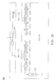
- FIG. 5A is a diagram of the source driver according to the preferred embodiment of the invention.
- the source driver 212 includes receivers 410, 412, transceivers 413, 415, a bus switch 422, wave generators 420, 421, and a driving unit 434.
- the transceiver 413 includes a control transceiver 414 and a data transceiver 424
- the transceiver 415 includes a control transceiver 416 and a data transceiver 426.
- the bus switch 422 includes two switches SW1 and SW2.
- the bus switch turns off the switches SW1 and SW2 such that the control transceiver 414 and 416 are disconnected from each other and the data transceiver 424 and 426 are disconnected from each other.
- the control bitstream C1 and the image data D1 received by the receiver 410 are transmitted to the control transceiver 414 and the data transceiver 424, respectively, and the control bitstream C2 and the image data D2 received by the receiver 410 are transmitted to the control transceiver 416 and the data transceiver 426, respectively.
- the source driver When the source driver, 212(1)-212(2), 212(4)-212(7), 212(9), or 212(10) in this embodiment, operates in a second operation mode, the receivers 410 and 412 are disabled, and the bus switch turns on the switches SW1 and SW2 such that the transceivers 413 and 415 are interconnected, that is, the data transceivers 424 and 426 are connected to each other and the control transceivers 414 and 416 are connected to each other.
- the source driver can transmit the control bitstream and the image data received to the next adjacent source driver in response to the designated transmission direction.
- the wave generators 420 and 421 receive the control bitstream C1 and C2, respectively, for generating source control signals S, such as STH(1), STH(2), POL(1), POL(2), TP(1) and TP(2), etc., and thus generating the gate control signals G, such as CPV(1), CPV(2), STV(1), STV(2), OEV(1), OEV(2) and etc.
- the control signals G are generated by one of the source drivers.
- one of the source drivers 212 such as 212(1) that is nearest to the gate driver 214, generates the gate control signals G, while the other source drivers 212 do not.
- two source drivers such as 212(1) and 212(10) that are respectively nearest to the gate drivers 214 and 216, generate the gate control signals G respectively for the gate drivers 214 and 216, while others do not.
- the driving unit 434 When receiving the signal STH, the driving unit 434 starts to latch image data D for converting to analog driving voltages in response to the signal POL, and then transmits the analog driving signals to the panel 210 after receiving the load signal TP.
- the wave generators 420 and 421 are both activated to receive the control bitstreams C1 and C2, respectively, and generate the source control signals S and the gate control signals G, while the control bitstream C1 and C2 are independent, and image data D1 and D2 are independent.
- the control bitstream C1 is the control bitstream C2
- the image data D1 is the image data D2
- the other wave generator in the second-operation-mode source driver can be disabled, omitted or still activated to generate the source control signals S and the gate control signals G.
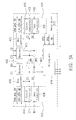
- FIG. 5B is a block diagram of the wave generator in FIG. 5A.
- Each of the wave generators 420 and 421 includes a parser 451, an ID recognizer 453, a signal generator 460 and an initiator 470.
- the parser 451 receives the control bitstream C to parse the control item, including the control field 312 and a data field 314, of a control packet, and sends the parsed control item to the ID recognizer 453, the signal generator 460 or the initiator 470.
- the control item with the identity event which is the STH event in this embodiment, is sent to the ID recognizer 453; the control item with the pull high event or the pull low event is set to the signal generator 460; the control item with the initialization event is sent to the initiator 470.
- FIG. 5C is a block diagram of the ID recognizer in FIG. 5B.
- the recognizer 453 includes a comparator 456.
- Each source driver has a unique chip identity IDp.
- the chip identity IDp is set externally, for example by, respectively, pulling high or pulling low the pins of the source driver on the glass substrate.
- the comparator 456 triggers the signal STH when the comparison of the chip identity IDp with a target identity IDt extracted from the control packet is matched.
- the assertion time td2 of the signal STH can be pre-determined in the comparator 456.
- FIG. 5D is a waveform diagram of control signal POL.
- the signal generator 460 pulls high the signal PH; when receiving the control with the corresponding pull low event L, the signal generator 460 pulls low the signal PL.
- the coupling of the signal PH and the signal PL is the signal POL.
- the other control signals such as CPV, STV, OEV, are also generated by the above-mentioned procedure.
- the control signal is not suitable to be generated by the pull high event and the pull low event if the assertion time of the high level of the control signal is less than 8 clocks, such as the control signal TP, since it takes 8 clocks for the wave generator to read a control packet.
- FIG. 5E is a waveform diagram of the generation of the control signal TP.
- the gate control signals G can also be generated according to the source control signals, such as STH or TP, as shown in FIG. 3.
- the signal CPV is generated according to the control signal STH.
- the control signal STH of the source driver 212(1) When the control signal STH of the source driver 212(1) is asserted, the counter thereof is activated, and the signal CPV is pulled high after a period td6, and, after a period tw4, the signal CPV is pulled low.
- the signal STV is generated according to the control signal STH.
- the control signal STH of the source driver 212(1) When the control signal STH of the source driver 212(1) is asserted, the signal STV is pulled high after a period td7 and then pulled low after a period tw5.
- the signal OEV is generated according to the control signal STH.
- the control signal STH of the source driver 212(1) When the control signal STH of the source driver 212(1) is asserted, the signal OEV is pulled high after
- the initiator 470 After receiving the control item with the initialization event, the initiator 470 outputs a DC value to set the corresponding parameter.
- the source driver of the present embodiment can reduce the control signal decay because the source control signals are generated by the source driver itself, not by the timing controller in the conventional manner.
- the present embodiment can reduce the number of wires from the timing controller to the gate driver because the source driver can generate the gate control signals and directly send them to the gate driver via the wires on the glass substrate.
- the quality of the gate control signals are thus improved because the lengths of the transmission wires are reduced.
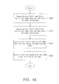
- FIG. 6A is a flowchart of a convergent transmission method for power saving.
- the source drivers 212(1)-212(5) in FIG. 2A are taken as an example.
- the source drivers 212(1) and 212(5) which have the farthest distances away from the timing controller225, receive the image data transmitted by the timing controller 225 via the source drivers.
- the power-saving mode is entered, which turns off the power for the data transceivers 424 and 426 of the source drivers 212(1) and 212(5), for example.
- the source drivers 212(2) and 212(4) which are the active ones having the farthest distances away from the timing controller 225, receive the image data and then enter the power-saving mode, which turns of the power for the data transceivers 424 and 426 of the source drivers 212(2) and 212(4), for example.
- the source driver 212(3) receives the image data from the timing controller 225 and then enters the power-saving mode. It is noted that, in the power-saving mode, the power for the control transceiver 416 and 414 of the source driver should not be turned off.
- each of the source drivers 212(1)-212(5) receives the load signal TP and then is activated to start to drive the panel 210.
- the transmission method can also apply to the source drivers 212(6)-212(10).
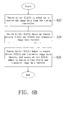
- FIG. 6B is a flowchart of a divergent transmission method for power saving.
- the source drivers 212(1)-212(5) in FIG. 2A are taken as an example.
- the source drivers 212(1)-212(5) enter the power-saving mode.
- the source driver 212(3) which is nearest to the timing controller 225, is activated to receive the image data transmitted by the timing controller 225.
- the source drivers 212(2) and 212(4) are activated to receive the image data.
- the source drivers 212(1) and 212(5) are waked up to receive the image data.
- the transmission method can also apply to the source drivers 212(6)-212(10).
- the power for data transceivers and the driving unit can be turned off.
- the data transceivers transmit the image data, which have large voltage swings and high frequency that make the power consumption great.
- the power-saving convergent/divergent transmission methods can reduce unnecessary data transmission for saving power.
- the power for the control transceivers of the source driver should not be turned off, so that the source driver can still receive the control bitstream and operate responsively.
- the convergent transmission method and the divergent transmission method can be applied at the same time.
- the source drivers 212(1)-212(3) can use the convergent transmission method, while the source drivers 212(4)-212(5) use the divergent transmission method, or vice versa.
Abstract
Description
- This application claims the benefit of People's Republic of
China application Serial No. 200510062824.2, filed March 31, 2005 - The invention relates in general to a liquid crystal display, and more particularly to the identifier of the source driver of a chip-on-glass liquid crystal display and the identifying method thereof.
- Liquid crystal displays (LCD) have become more and more popular in computer monitors or TVs due to their light weight, flatness and low radiation, compared with the CRT monitor. In addition to improving the display quality of LCDs, such as color, contrast and brightness, the manufacturers try to improve the manufacturing process to reduce the cost and manufacturing time.
- The LCD includes a timing controller, source drivers and at least one gate driver to drive its liquid crystal panel. Conventionally, the timing controller is welded on a control print circuit board, the source drivers are welded on an X-board, and the gate driver is welded on a Y-board. The control print circuit board connects to the X-board via flexible printed circuit boards (FPCs), while the X-board and the Y board each connects to the liquid crystal panel via other FPCs. Therefore, the conventional LCD requires at least three boards to be connected to the panel and the manufacturing process is thus complex. In order to simplify the manufacturing process, the chip-on-glass (COG) LCD has been developed:
- FIG. 1 is diagram of a conventional COG LCD. The
COG LCD 100 includes apanel 110, a plurality ofsource drivers 112, at least onegate driver 114, aprinted circuit board 120 and a plurality of flexibleprinted circuit boards 130. Thesource drivers 112 and thegate driver 114 are disposed on the glass substrate of thepanel 110 and electrically connect to the printedcircuit board 120 via the flexibleprinted circuit boards 130. The timing controller (not shown in FIG. 1) is disposed on the printedcircuit board 120, and outputs image data and control signals to thesource drivers 112 and thegate driver 114. InCOG LCD 100, only one board (PCB 120), instead of three, is required to connect to thepanel 110 via the FPCs 130. Therefore, the manufacturing process is simplified. - However, the manufacturing process of COG LCD is still not simplified enough because a plurality of flexible printed circuit boards are needed, and in the above example in FIG. 1, the number of flexible printed circuit boards is 11. The flexible printed boards need a plurality of contact points with the liquid crystal panel and the possibility of electrical contact failure is thus increased.
- It is therefore an object of the invention to provide a COG LCD that reduces the number of flexible printed circuit boards and to provide a transmission method for the LCD.
- It is another object of the invention to provide a method for generating gate control signals for reducing the number of flexible printed circuit boards.
- Furthermore, it is another object of the invention to provide an identifier of the source driver of the COG LCD and an identifying method thereof.
- It is another object of the invention to provide a source driver for single-way or dual-way transmission of the image data and the control signals from the timing controller.
- It is another object of the invention to provide a method for transmitting control signals by packets so as to reduce the number of transmission lines to few or only one and reduce the number of flexible printed circuit boards.
- It is another object of the invention to provide a method for power management so as to save power consumption of the COG LCD.
- The invention achieves the above-identified objects by providing an identifier for identifying a source driver of a chip-on-glass liquid crystal display. The identifier includes a comparator for receiving a chip identity and a target identity, and generates a triggering signal to activate the source driver if the chip identity coincides with the target identity.
- Other objects, features, and advantages of the invention will become apparent from the following detailed description of the preferred but non-limiting embodiments. The following description is made with reference to the accompanying drawings.
- FIG. 1 is diagram of a conventional COG LCD.
- FIG. 2A is a diagram of a chip-on-glass (COG) liquid crystal display (LCD) according to a preferred embodiment of the invention.
- FIG. 2B is a diagram of a COG LCD according to another preferred embodiment of the invention.
- FIG. 3 is a diagram of control signals of the source drivers and the gate drivers of the LCD.
- FIG. 4 is a format diagram of a control packet.
- FIG. 5A is a diagram of the source driver according to the preferred embodiment of the invention.
- FIG. 5B is a block diagram of the wave generator in FIG. 5A.
- FIG. 5C is a block diagram of the ID recognizer in FIG. 5B.
- FIG. 5D is a waveform diagram of control signal POL.
- FIG. 5E is a waveform diagram of the generation of the control signal TP.
- FIG. 6A is a flowchart of a convergent transmission method for power saving.
- FIG. 6B is a flowchart of a divergent transmission method for power saving.
- FIG. 2A is a diagram of a chip-on-glass (COG) liquid crystal display (LCD) according to a preferred embodiment of the invention. The
LCD 200 includes apanel 210, a plurality of source drivers (S/D) 212(1)-212(10), at least onegate driver 214, aprinted circuit board 220 and flexible printed circuit boards (FPC) 230 and 232. Thesource drivers 212 andgate driver 214 are disposed on the glass substrate of thepanel 210 by chip-on-glass technology. Thetiming controller 225 is disposed on the printedcircuit board 220 for outputting image data and control signals both to source drivers 212(3) and 212(8) respectively via the flexible printedcircuit boards gate driver 214, can generate gate control signals G to thegate driver 214. The reason to choose the source driver nearest to thegate driver 212 is to reduce the length of the wire there between so as to effectively reduce the distortions and delays of the gate control signals G. It is worthy of noting that other source drives can also be used to generate the gate control signals G, not just limited to the source driver 212(1). In this embodiment, the number of flexible printed circuit boards are greatly reduced to 2 because the LCD uses the wires disposed on the glass substrate for transmitting the image data and the control signals. - Each of the
source drivers 212 has a first operation mode and a second operation mode. The source driver 212(3) and the source driver 212(8) are set to the first operation mode to execute the dual-way transmission. That is, the source driver 212(3) and the source driver 212(8) each receives the image data and control signals from thetiming controller 225 and transmits them to the neighboring source drivers at both the right side and the left side thereof. Taking the source driver 212(3) for example, the source driver 212(3) can simultaneously transmit the image data and control signals to both the neighboring source driver 212(2) and 212(4), which are located at the two sides of the source driver 212(3). The source drivers 212(1), 212(2), 212(4)-212(7), 212(9) and 212(10) are set to the second operation mode to execute single-way transmission, and are not directly connected to thetiming controller 225. That is, the source drivers 212(1), 212(2), 212(4)-212(7), 212(9) and 212(10) each can receive the image data and the control signals from the right (or left) source driver and transmit them to the left (or right) source driver. Taking the source driver 212(2) for example, it receives the image data and the control signals from the source driver 212(3) at the right side thereof and transmits them to the source driver 212(1) at the left side thereof. In the embodiment, theLCD 200 is a big screen monitor having 10 source drivers and two flexible printedcircuit board - In the embodiment, the source drivers are divided into a left group including source drivers 212(1)-212(5) and a right group including source drivers 212(6)-212(10). The flexible printed
circuit board 230 connects to the center source drivers 212(3) of the left group, and the flexible printedcircuit board 232 connects to the center source drivers 212(8) of the right group, such that the distortions and delays of signals, caused by the parasitic capacitance and resistance, can be minimized. On the other hand, the source drivers can also be divided into more than three groups and each group directly connects to the timing controller via a flexible printed circuit board, so long as the distortions and delays of the signals are acceptable. - FIG. 2B is a diagram of a COG LCD 250 according to another preferred embodiment of the invention. Compared with the
LCD 200, the LCD 250 further includes agate driver 216 at the right side of thepanel 210. Thegate drivers panel 210 from two sides thereof. The other elements of LCD 250 are the same as those as described above. - FIG. 3 is a diagram of control signals of the source drivers and the gate drivers of the LCD. The control signals include gate control signals G and source control signals S. The gate control signals G include a gate driver start signal STV for representing the start of a frame, a gate clock signal CPV for enabling a gate line, and a gate driver output enable signal OEV for defining the enabled duration of the gate line. The source control signals S include a source driver start signal STH for notifying the source driver to start to prepare the data of a horizontal line, a data enable signal DE for starting to receive data, a load signal TP for starting to output driving voltages to the data lines, and a polarization control signal POL for controlling the polarization inversion.
- When the source driver start signal STH is asserted, the
source driver 212 starts to prepare to receive data, and after a period td1, the data enable signal DE is asserted such that thetiming controller 225 starts to output the image data to thesource drivers 212. Thesource drivers 212 generate the driving voltage with the polarization designated by the polarization control signal POL and then outputs the driving voltages to thepanel 210 according to the load signal Tp. - In the
conventional LCD 100, the control signals are outputted by the timing controller directly to eachsource driver 112 and thegate driver 114. Each control signal conventionally needs at least one wire to transmit, and thus a plurality of wires are required. The control signals are easily distorted and delayed because the wires between the timing controller and the source drivers and the gate driver have parasitic capacitance and resistance. - In the present embodiment, the
timing controller 225 integrates the control signals into a control bitstream C and transmits it by a wire to thesource drivers 212. For example, the control signals can be packed into a plurality of control packets, each representing an event relevant to a control signal. Thetiming controller 225 can designate onesource driver 212 to receive the control packet by a target identification. The target identification is, for example, included in the control packet for each source driver to identify. After receiving the control packet, thesource driver 212 can decode the control packet to generate the control signal. Therefore, the number of the wires required to transmit the control signals is thus greatly reduced in the present embodiment. - The
source driver 212 has a built-in identification so as to identify whether a received control packet is for its own by comparing the target identification of the control packet with the built-in identification. - Conventionally the control signals are each transmitted by a wire from the timing controller to the source driver/gate driver. The source drivers and the gate driver each needs a plurality of control signals and thus the number of the wires for transmitting the control signals is great. Therefore, number of wires in the conventional flexible printed circuit board is also great. The conventional structure thus requires a flexible printed circuit board of high cost and quality. The lengths of the wires between the timing controller and the source drivers/gate driver are so long as to incur delays and distortions of the signals.
- In the present embodiment, the
timing controller 225 transmits a control bitstream C to the source driver a minimum of wires. The control bitstream C includes a plurality of control packets, each representing an event of one corresponding control signal, such as a pull high event or a pull low event. After receiving the control packet, thesource driver 212 generates the corresponding control signal by pulling high or pulling low accordingly. - FIG. 4 is a format diagram of a control packet. A control packet includes a
header field 310 and a control item, which includes acontrol field 312 and adata field 314. Theheader field 310 records a predetermined pattern for identifying the start of a packet, for example, 0x11111. Thecontrol field 312 records the type of the event, such as the STH event, the TP event, the pull high event, the pull low event and the initialization event. The data field 314 records the parameters of the event. - In the present embodiment, each control packet has 16 bits. If receiving the control packet by dual-edge sampling, it takes 8 clocks to read one control packet. That is, the control signal generated by a pull high event and a pull low event must remain at high level for at least assertion time of 8 clocks. The control signals POL, CPV, STV, OEV can each be generated by a pull high event and a pull low event. The control signal that has assertion time of less than 8 clocks, such as control signals STH and TP, are generated respectively by the STH event and the TP event. After receiving the STH event/TP event, the source driver pulls high the control signal STH/TP for a pre-determined period td2/tw1 and then pulls low the control signal STH/TP. It is worth noticing that the sampling method for receiving the control packet is not limited to dual-edge sampling. Rising-edge sampling or falling-edge sampling can also be used.
- In regard to the control packet having the
control field 312 recording the STH event, thedata field 314 thereof records the target identification. For example, the source drivers 212(1)-212(10) have the built-in identifications of 0x0001-0x1010, respectively. After receiving the control packet with STH event, the source driver compares the target identification of this control packet with the built-in identification, pulls high the control signal STH if the comparison is matched, and then pulls low the control signal STH after a period td2. - From FIG. 3, it can be seen that the control signals TP and CPV are pulled high at the same time, so after receiving the control packet with TP event, control signals TP and CPV are pulled high. The control signal TP is then pulled low after a period tw1, and the control signal CPV is pulled low after receiving the control packet with pull low event of CPV.
- Control signals POL, STV and OEV are generated by a pull high event and a pull low event. In regard to the control packet with the
control field 312 recording a pull high event, itsdata field 314 designates which signal is to be pulled high. In regard to the control packet with thecontrol field 312 recording a pull low event, itsdata field 314 designates which signal is to be pulled low. - In regard to the control packet with the
control field 312 recording an initialization event, setting several kinds of initialization can be set, such as the fan out of the source drivers. Other kinds of events can also be represented by the control packets. - In the present embodiment, as a minimum of wires is required to transmit the control bitstream C, the number of wires connecting the timing controller and the source drivers are greatly reduced, the layout of the circuit is simplified, and stability is enhanced. In addition, the control bitstream C can integrate only a part of the control signals and leave other parts of the control signals to be transmitted respectively in independent wires. Although not all the control signals are integrated to the control bitstream, the number of wires can still be reduced.
- FIG. 5A is a diagram of the source driver according to the preferred embodiment of the invention. The
source driver 212 includesreceivers transceivers bus switch 422,wave generators driving unit 434. Thetransceiver 413 includes acontrol transceiver 414 and adata transceiver 424, and thetransceiver 415 includes acontrol transceiver 416 and adata transceiver 426. - The
bus switch 422 includes two switches SW1 and SW2. When the source driver, 212(3) or 212(8) in this embodiment, operates at a first operation mode, the bus switch turns off the switches SW1 and SW2 such that thecontrol transceiver data transceiver receiver 410 are transmitted to thecontrol transceiver 414 and thedata transceiver 424, respectively, and the control bitstream C2 and the image data D2 received by thereceiver 410 are transmitted to thecontrol transceiver 416 and thedata transceiver 426, respectively. - When the source driver, 212(1)-212(2), 212(4)-212(7), 212(9), or 212(10) in this embodiment, operates in a second operation mode, the
receivers transceivers data transceivers control transceivers - The
wave generators LCD 200 in FIG. 2A, one of thesource drivers 212, such as 212(1) that is nearest to thegate driver 214, generates the gate control signals G, while theother source drivers 212 do not. In the LCD 250 in FIG. 2B, two source drivers, such as 212(1) and 212(10) that are respectively nearest to thegate drivers gate drivers - When receiving the signal STH, the driving
unit 434 starts to latch image data D for converting to analog driving voltages in response to the signal POL, and then transmits the analog driving signals to thepanel 210 after receiving the load signal TP. - In the first-operation-mode source driver, such as 212(3), the
wave generators wave generators - FIG. 5B is a block diagram of the wave generator in FIG. 5A. Each of the
wave generators parser 451, anID recognizer 453, asignal generator 460 and aninitiator 470. Theparser 451 receives the control bitstream C to parse the control item, including thecontrol field 312 and adata field 314, of a control packet, and sends the parsed control item to theID recognizer 453, thesignal generator 460 or theinitiator 470. The control item with the identity event, which is the STH event in this embodiment, is sent to theID recognizer 453; the control item with the pull high event or the pull low event is set to thesignal generator 460; the control item with the initialization event is sent to theinitiator 470. - FIG. 5C is a block diagram of the ID recognizer in FIG. 5B. The
recognizer 453 includes acomparator 456. Each source driver has a unique chip identity IDp. The chip identity IDp is set externally, for example by, respectively, pulling high or pulling low the pins of the source driver on the glass substrate. Thecomparator 456 triggers the signal STH when the comparison of the chip identity IDp with a target identity IDt extracted from the control packet is matched. The assertion time td2 of the signal STH can be pre-determined in thecomparator 456. - The
signal generator 460 pulls high the corresponding signal after receiving the control item with the pull high event. The level of the pull-high signal is maintained until thesignal generator 460 receives the corresponding control item with the pull low event. Taking generation of the control signal POL for example, FIG. 5D is a waveform diagram of control signal POL. When receiving the control item with the pull high event H, thesignal generator 460 pulls high the signal PH; when receiving the control with the corresponding pull low event L, thesignal generator 460 pulls low the signal PL. The coupling of the signal PH and the signal PL is the signal POL. The other control signals, such as CPV, STV, OEV, are also generated by the above-mentioned procedure. - The control signal is not suitable to be generated by the pull high event and the pull low event if the assertion time of the high level of the control signal is less than 8 clocks, such as the control signal TP, since it takes 8 clocks for the wave generator to read a control packet. FIG. 5E is a waveform diagram of the generation of the control signal TP. When receiving the control item with the pull high event H of the control signal TP, the
signal generator 460 pulls high the signal TH, then counts for a pre-determined period tw1, and then pulls low the signal TL. The coupling of the signal TH and the signal TL is the control signal TP. - The gate control signals G can also be generated according to the source control signals, such as STH or TP, as shown in FIG. 3. The signal CPV is generated according to the control signal STH. When the control signal STH of the source driver 212(1) is asserted, the counter thereof is activated, and the signal CPV is pulled high after a period td6, and, after a period tw4, the signal CPV is pulled low. The signal STV is generated according to the control signal STH. When the control signal STH of the source driver 212(1) is asserted, the signal STV is pulled high after a period td7 and then pulled low after a period tw5. The signal OEV is generated according to the control signal STH. When the control signal STH of the source driver 212(1) is asserted, the signal OEV is pulled high after a period td8 passed and pulled low after a period tw6 passed.
- After receiving the control item with the initialization event, the
initiator 470 outputs a DC value to set the corresponding parameter. - The source driver of the present embodiment can reduce the control signal decay because the source control signals are generated by the source driver itself, not by the timing controller in the conventional manner.
- In addition, the present embodiment can reduce the number of wires from the timing controller to the gate driver because the source driver can generate the gate control signals and directly send them to the gate driver via the wires on the glass substrate. The quality of the gate control signals are thus improved because the lengths of the transmission wires are reduced.
- FIG. 6A is a flowchart of a convergent transmission method for power saving. The source drivers 212(1)-212(5) in FIG. 2A are taken as an example. First, at
step 610, the source drivers 212(1) and 212(5), which have the farthest distances away from the timing controller225, receive the image data transmitted by thetiming controller 225 via the source drivers. The power-saving mode is entered, which turns off the power for thedata transceivers step 612, the source drivers 212(2) and 212(4), which are the active ones having the farthest distances away from thetiming controller 225, receive the image data and then enter the power-saving mode, which turns of the power for thedata transceivers step 614, the source driver 212(3) receives the image data from thetiming controller 225 and then enters the power-saving mode. It is noted that, in the power-saving mode, the power for thecontrol transceiver step 616, each of the source drivers 212(1)-212(5) receives the load signal TP and then is activated to start to drive thepanel 210. The transmission method can also apply to the source drivers 212(6)-212(10). - FIG. 6B is a flowchart of a divergent transmission method for power saving. The source drivers 212(1)-212(5) in FIG. 2A are taken as an example. First, the source drivers 212(1)-212(5) enter the power-saving mode. Next, at
step 622, the source driver 212(3), which is nearest to thetiming controller 225, is activated to receive the image data transmitted by thetiming controller 225. Next, atstep 624, the source drivers 212(2) and 212(4) are activated to receive the image data. Next, atstep 626, the source drivers 212(1) and 212(5) are waked up to receive the image data. The transmission method can also apply to the source drivers 212(6)-212(10). - In the power-saving mode, at least the power for data transceivers and the driving unit can be turned off. The data transceivers transmit the image data, which have large voltage swings and high frequency that make the power consumption great. Thus the power-saving convergent/divergent transmission methods can reduce unnecessary data transmission for saving power. The power for the control transceivers of the source driver should not be turned off, so that the source driver can still receive the control bitstream and operate responsively.
- The convergent transmission method and the divergent transmission method can be applied at the same time. For example, the source drivers 212(1)-212(3) can use the convergent transmission method, while the source drivers 212(4)-212(5) use the divergent transmission method, or vice versa.
- While the invention has been described by way of example and in terms of a preferred embodiment, it is to be understood that the invention is not limited thereto. On the contrary, it is intended to cover various modifications and similar arrangements and procedures, and the scope of the appended claims therefore should be accorded the broadest interpretation so as to encompass all such modifications and similar arrangements and procedures.
Claims (8)
- An identifier for identifying a source driver of a chip-on-glass liquid crystal display, comprising:a comparator for receiving a chip identity and a target identity, andgenerating a triggering signal to activate the source driver if the chip identity coincides with the target identity.
- The identifier according to claim 1, wherein the chip identity is pre-determined by respectively pulling high or low pins of the source driver on the glass substrate.
- The identifier according to claim 1, wherein the triggering signal is a source driver start signal (STH signal).
- The identifier according to claim 1, wherein the assertion time of the triggering signal is predetermined.
- An identifying method for identifying a source driver of a chip-on-glass liquid crystal display, comprising:receiving a chip identity and a target identity from the source driver;comparing the chip identity and the target identity; andgenerating a triggering signal to activate the source driver if the chip identity coincides with the target identity.
- The method according to claim 5, wherein the chip identity is pre-determined by respectively pulling high or low pins of the source driver on the glass substrate.
- The identifier according to claim 1, wherein the triggering signal is a source driver start signal (STH signal).
- The identifier according to claim 1, wherein the assertion time of the triggering signal is predetermined.
Applications Claiming Priority (1)
| Application Number | Priority Date | Filing Date | Title |
|---|---|---|---|
| CNB2005100628242A CN100433118C (en) | 2005-03-31 | 2005-03-31 | Recognition apparatus and method for source driver of chip-on-glass packaged liquid crystal display |
Publications (2)
| Publication Number | Publication Date |
|---|---|
| EP1708154A2 true EP1708154A2 (en) | 2006-10-04 |
| EP1708154A3 EP1708154A3 (en) | 2007-08-15 |
Family
ID=36608213
Family Applications (1)
| Application Number | Title | Priority Date | Filing Date |
|---|---|---|---|
| EP06005205A Withdrawn EP1708154A3 (en) | 2005-03-31 | 2006-03-14 | Identifier of source driver of chip-on-glass liquid crystal display and identifying method thereof |
Country Status (2)
| Country | Link |
|---|---|
| EP (1) | EP1708154A3 (en) |
| CN (1) | CN100433118C (en) |
Families Citing this family (1)
| Publication number | Priority date | Publication date | Assignee | Title |
|---|---|---|---|---|
| CN104157250B (en) * | 2014-07-25 | 2018-11-23 | 京东方科技集团股份有限公司 | Display device and preparation method thereof |
Citations (1)
| Publication number | Priority date | Publication date | Assignee | Title |
|---|---|---|---|---|
| US6335720B1 (en) | 1995-04-27 | 2002-01-01 | Canon Kabushiki Kaisha | Data transfer method, display driving circuit using the method, and image display apparatus |
Family Cites Families (3)
| Publication number | Priority date | Publication date | Assignee | Title |
|---|---|---|---|---|
| CN1044292C (en) * | 1993-05-13 | 1999-07-21 | 卡西欧计算机公司 | Display driving device |
| JP3508837B2 (en) * | 1999-12-10 | 2004-03-22 | インターナショナル・ビジネス・マシーンズ・コーポレーション | Liquid crystal display device, liquid crystal controller, and video signal transmission method |
| JP3618086B2 (en) * | 2000-07-24 | 2005-02-09 | シャープ株式会社 | Multiple column electrode drive circuit and display device |
-
2005
- 2005-03-31 CN CNB2005100628242A patent/CN100433118C/en not_active Expired - Fee Related
-
2006
- 2006-03-14 EP EP06005205A patent/EP1708154A3/en not_active Withdrawn
Patent Citations (1)
| Publication number | Priority date | Publication date | Assignee | Title |
|---|---|---|---|---|
| US6335720B1 (en) | 1995-04-27 | 2002-01-01 | Canon Kabushiki Kaisha | Data transfer method, display driving circuit using the method, and image display apparatus |
Also Published As
| Publication number | Publication date |
|---|---|
| CN1841481A (en) | 2006-10-04 |
| CN100433118C (en) | 2008-11-12 |
| EP1708154A3 (en) | 2007-08-15 |
Similar Documents
| Publication | Publication Date | Title |
|---|---|---|
| US7830353B2 (en) | Method for transmitting control signal of chip-on-glass liquid crystal display | |
| US7916113B2 (en) | Method and apparatus for generating gate control signal of liquid crystal display | |
| US8040312B2 (en) | Chip-on-glass liquid crystal display and data transmission method for the same | |
| EP1708166B1 (en) | Chip-on-glass liquid crystal display and data transmission method for the same | |
| US7359290B2 (en) | Power saving method of a chip-on-glass liquid crystal display | |
| US7518589B2 (en) | Liquid crystal display device and method for driving the same | |
| US20130002621A1 (en) | Display device and driving circuit | |
| US8125435B2 (en) | Identifier of source driver of chip-on-glass liquid crystal display and identifying method thereof | |
| EP1708167B1 (en) | Method and apparatus for generating gate control signal of liquid crystal display | |
| EP1708168B1 (en) | Power saving method of a chip-on-glass liquid crystal display | |
| US20110050554A1 (en) | Display device and backlight control method thereof | |
| EP1708154A2 (en) | Identifier of source driver of chip-on-glass liquid crystal display and identifying method thereof | |
| US20100164939A1 (en) | Display and communication method thereof | |
| RU2645289C2 (en) | Mode of excitation and control circuit for the lcd panel | |
| US20080192041A1 (en) | Liquid crystal display for multi-scanning and driving method thereof | |
| US20080048965A1 (en) | Driving system of liquid crystal display | |
| US20030142083A1 (en) | Driver circuit for LCDM |
Legal Events
| Date | Code | Title | Description |
|---|---|---|---|
| PUAI | Public reference made under article 153(3) epc to a published international application that has entered the european phase |
Free format text: ORIGINAL CODE: 0009012 |
|
| AK | Designated contracting states |
Kind code of ref document: A2 Designated state(s): AT BE BG CH CY CZ DE DK EE ES FI FR GB GR HU IE IS IT LI LT LU LV MC NL PL PT RO SE SI SK TR |
|
| AX | Request for extension of the european patent |
Extension state: AL BA HR MK YU |
|
| PUAL | Search report despatched |
Free format text: ORIGINAL CODE: 0009013 |
|
| AK | Designated contracting states |
Kind code of ref document: A3 Designated state(s): AT BE BG CH CY CZ DE DK EE ES FI FR GB GR HU IE IS IT LI LT LU LV MC NL PL PT RO SE SI SK TR |
|
| AX | Request for extension of the european patent |
Extension state: AL BA HR MK YU |
|
| 17P | Request for examination filed |
Effective date: 20080206 |
|
| AKX | Designation fees paid |
Designated state(s): GB NL |
|
| REG | Reference to a national code |
Ref country code: DE Ref legal event code: 8566 |
|
| 17Q | First examination report despatched |
Effective date: 20100415 |
|
| STAA | Information on the status of an ep patent application or granted ep patent |
Free format text: STATUS: THE APPLICATION IS DEEMED TO BE WITHDRAWN |
|
| 18D | Application deemed to be withdrawn |
Effective date: 20161001 |