EP1783789A1 - Thin film device and thin film inductor - Google Patents
Thin film device and thin film inductor Download PDFInfo
- Publication number
- EP1783789A1 EP1783789A1 EP06020617A EP06020617A EP1783789A1 EP 1783789 A1 EP1783789 A1 EP 1783789A1 EP 06020617 A EP06020617 A EP 06020617A EP 06020617 A EP06020617 A EP 06020617A EP 1783789 A1 EP1783789 A1 EP 1783789A1
- Authority
- EP
- European Patent Office
- Prior art keywords
- film
- substrate
- thin film
- magnetic
- surface roughness
- Prior art date
- Legal status (The legal status is an assumption and is not a legal conclusion. Google has not performed a legal analysis and makes no representation as to the accuracy of the status listed.)
- Withdrawn
Links
- 239000010409 thin film Substances 0.000 title claims abstract description 118
- 239000010408 film Substances 0.000 claims abstract description 255
- 239000000758 substrate Substances 0.000 claims abstract description 131
- 230000003746 surface roughness Effects 0.000 claims abstract description 82
- 230000014509 gene expression Effects 0.000 claims abstract description 66
- 230000035699 permeability Effects 0.000 abstract description 23
- 230000000694 effects Effects 0.000 abstract description 11
- 230000001788 irregular Effects 0.000 abstract description 4
- 239000010410 layer Substances 0.000 description 18
- 238000000034 method Methods 0.000 description 14
- 239000000463 material Substances 0.000 description 11
- 230000004048 modification Effects 0.000 description 10
- 238000012986 modification Methods 0.000 description 10
- 230000006870 function Effects 0.000 description 8
- VYPSYNLAJGMNEJ-UHFFFAOYSA-N Silicium dioxide Chemical compound O=[Si]=O VYPSYNLAJGMNEJ-UHFFFAOYSA-N 0.000 description 7
- PNEYBMLMFCGWSK-UHFFFAOYSA-N Alumina Chemical compound [O-2].[O-2].[O-2].[Al+3].[Al+3] PNEYBMLMFCGWSK-UHFFFAOYSA-N 0.000 description 5
- 239000010949 copper Substances 0.000 description 5
- 239000000696 magnetic material Substances 0.000 description 5
- 229910052814 silicon oxide Inorganic materials 0.000 description 5
- 229910000859 α-Fe Inorganic materials 0.000 description 5
- RYGMFSIKBFXOCR-UHFFFAOYSA-N Copper Chemical compound [Cu] RYGMFSIKBFXOCR-UHFFFAOYSA-N 0.000 description 4
- 239000002131 composite material Substances 0.000 description 4
- 229910052802 copper Inorganic materials 0.000 description 4
- 230000005415 magnetization Effects 0.000 description 4
- 238000004519 manufacturing process Methods 0.000 description 4
- 239000002356 single layer Substances 0.000 description 4
- PXHVJJICTQNCMI-UHFFFAOYSA-N Nickel Chemical compound [Ni] PXHVJJICTQNCMI-UHFFFAOYSA-N 0.000 description 3
- XUIMIQQOPSSXEZ-UHFFFAOYSA-N Silicon Chemical compound [Si] XUIMIQQOPSSXEZ-UHFFFAOYSA-N 0.000 description 3
- 229910045601 alloy Inorganic materials 0.000 description 3
- 239000000956 alloy Substances 0.000 description 3
- 239000004020 conductor Substances 0.000 description 3
- 230000007246 mechanism Effects 0.000 description 3
- 239000010703 silicon Substances 0.000 description 3
- 229910052710 silicon Inorganic materials 0.000 description 3
- 238000004804 winding Methods 0.000 description 3
- 229910001030 Iron–nickel alloy Inorganic materials 0.000 description 2
- 229910001362 Ta alloys Inorganic materials 0.000 description 2
- ZGWQKLYPIPNASE-UHFFFAOYSA-N [Co].[Zr].[Ta] Chemical compound [Co].[Zr].[Ta] ZGWQKLYPIPNASE-UHFFFAOYSA-N 0.000 description 2
- 230000009471 action Effects 0.000 description 2
- 230000002411 adverse Effects 0.000 description 2
- 238000009713 electroplating Methods 0.000 description 2
- 230000002708 enhancing effect Effects 0.000 description 2
- 238000005530 etching Methods 0.000 description 2
- 229910052751 metal Inorganic materials 0.000 description 2
- 239000002184 metal Substances 0.000 description 2
- 239000000203 mixture Substances 0.000 description 2
- 229920002120 photoresistant polymer Polymers 0.000 description 2
- 230000008569 process Effects 0.000 description 2
- 239000011347 resin Substances 0.000 description 2
- 229920005989 resin Polymers 0.000 description 2
- 238000001039 wet etching Methods 0.000 description 2
- 238000012935 Averaging Methods 0.000 description 1
- 229910000531 Co alloy Inorganic materials 0.000 description 1
- 229910003321 CoFe Inorganic materials 0.000 description 1
- 229910001313 Cobalt-iron alloy Inorganic materials 0.000 description 1
- 229910000640 Fe alloy Inorganic materials 0.000 description 1
- XEEYBQQBJWHFJM-UHFFFAOYSA-N Iron Chemical compound [Fe] XEEYBQQBJWHFJM-UHFFFAOYSA-N 0.000 description 1
- 229910001257 Nb alloy Inorganic materials 0.000 description 1
- 239000004642 Polyimide Substances 0.000 description 1
- BQCADISMDOOEFD-UHFFFAOYSA-N Silver Chemical compound [Ag] BQCADISMDOOEFD-UHFFFAOYSA-N 0.000 description 1
- 229910001297 Zn alloy Inorganic materials 0.000 description 1
- BDVUYXNQWZQBBN-UHFFFAOYSA-N [Co].[Zr].[Nb] Chemical compound [Co].[Zr].[Nb] BDVUYXNQWZQBBN-UHFFFAOYSA-N 0.000 description 1
- KOMIMHZRQFFCOR-UHFFFAOYSA-N [Ni].[Cu].[Zn] Chemical compound [Ni].[Cu].[Zn] KOMIMHZRQFFCOR-UHFFFAOYSA-N 0.000 description 1
- 230000004075 alteration Effects 0.000 description 1
- 229910000808 amorphous metal alloy Inorganic materials 0.000 description 1
- 230000008901 benefit Effects 0.000 description 1
- 239000000919 ceramic Substances 0.000 description 1
- 239000011248 coating agent Substances 0.000 description 1
- 238000000576 coating method Methods 0.000 description 1
- 229910017052 cobalt Inorganic materials 0.000 description 1
- 239000010941 cobalt Substances 0.000 description 1
- GUTLYIVDDKVIGB-UHFFFAOYSA-N cobalt atom Chemical compound [Co] GUTLYIVDDKVIGB-UHFFFAOYSA-N 0.000 description 1
- 229910052681 coesite Inorganic materials 0.000 description 1
- 238000012790 confirmation Methods 0.000 description 1
- 229910052593 corundum Inorganic materials 0.000 description 1
- 229910052906 cristobalite Inorganic materials 0.000 description 1
- 239000013078 crystal Substances 0.000 description 1
- 230000007547 defect Effects 0.000 description 1
- 238000013461 design Methods 0.000 description 1
- 238000010586 diagram Methods 0.000 description 1
- 238000001312 dry etching Methods 0.000 description 1
- 239000011521 glass Substances 0.000 description 1
- 230000006872 improvement Effects 0.000 description 1
- 239000012535 impurity Substances 0.000 description 1
- 239000011810 insulating material Substances 0.000 description 1
- 230000005381 magnetic domain Effects 0.000 description 1
- 230000005389 magnetism Effects 0.000 description 1
- 150000002739 metals Chemical class 0.000 description 1
- 229910052759 nickel Inorganic materials 0.000 description 1
- 238000007747 plating Methods 0.000 description 1
- 238000005498 polishing Methods 0.000 description 1
- 229920001721 polyimide Polymers 0.000 description 1
- 238000012545 processing Methods 0.000 description 1
- 230000009467 reduction Effects 0.000 description 1
- 239000004065 semiconductor Substances 0.000 description 1
- 239000000377 silicon dioxide Substances 0.000 description 1
- 229910052709 silver Inorganic materials 0.000 description 1
- 239000004332 silver Substances 0.000 description 1
- 238000000992 sputter etching Methods 0.000 description 1
- 229910052682 stishovite Inorganic materials 0.000 description 1
- 229910052905 tridymite Inorganic materials 0.000 description 1
- 229910001845 yogo sapphire Inorganic materials 0.000 description 1
Images


Classifications
-
- H—ELECTRICITY
- H01—ELECTRIC ELEMENTS
- H01F—MAGNETS; INDUCTANCES; TRANSFORMERS; SELECTION OF MATERIALS FOR THEIR MAGNETIC PROPERTIES
- H01F27/00—Details of transformers or inductances, in general
-
- H—ELECTRICITY
- H01—ELECTRIC ELEMENTS
- H01F—MAGNETS; INDUCTANCES; TRANSFORMERS; SELECTION OF MATERIALS FOR THEIR MAGNETIC PROPERTIES
- H01F17/00—Fixed inductances of the signal type
- H01F17/0006—Printed inductances
-
- B—PERFORMING OPERATIONS; TRANSPORTING
- B81—MICROSTRUCTURAL TECHNOLOGY
- B81C—PROCESSES OR APPARATUS SPECIALLY ADAPTED FOR THE MANUFACTURE OR TREATMENT OF MICROSTRUCTURAL DEVICES OR SYSTEMS
- B81C1/00—Manufacture or treatment of devices or systems in or on a substrate
- B81C1/00349—Creating layers of material on a substrate
- B81C1/0038—Processes for creating layers of materials not provided for in groups B81C1/00357 - B81C1/00373
-
- H—ELECTRICITY
- H01—ELECTRIC ELEMENTS
- H01F—MAGNETS; INDUCTANCES; TRANSFORMERS; SELECTION OF MATERIALS FOR THEIR MAGNETIC PROPERTIES
- H01F10/00—Thin magnetic films, e.g. of one-domain structure
-
- H—ELECTRICITY
- H01—ELECTRIC ELEMENTS
- H01F—MAGNETS; INDUCTANCES; TRANSFORMERS; SELECTION OF MATERIALS FOR THEIR MAGNETIC PROPERTIES
- H01F17/00—Fixed inductances of the signal type
- H01F17/0006—Printed inductances
- H01F2017/0046—Printed inductances with a conductive path having a bridge
-
- H—ELECTRICITY
- H01—ELECTRIC ELEMENTS
- H01F—MAGNETS; INDUCTANCES; TRANSFORMERS; SELECTION OF MATERIALS FOR THEIR MAGNETIC PROPERTIES
- H01F41/00—Apparatus or processes specially adapted for manufacturing or assembling magnets, inductances or transformers; Apparatus or processes specially adapted for manufacturing materials characterised by their magnetic properties
- H01F41/02—Apparatus or processes specially adapted for manufacturing or assembling magnets, inductances or transformers; Apparatus or processes specially adapted for manufacturing materials characterised by their magnetic properties for manufacturing cores, coils, or magnets
- H01F41/04—Apparatus or processes specially adapted for manufacturing or assembling magnets, inductances or transformers; Apparatus or processes specially adapted for manufacturing materials characterised by their magnetic properties for manufacturing cores, coils, or magnets for manufacturing coils
- H01F41/041—Printed circuit coils
- H01F41/042—Printed circuit coils by thin film techniques
-
- H—ELECTRICITY
- H01—ELECTRIC ELEMENTS
- H01L—SEMICONDUCTOR DEVICES NOT COVERED BY CLASS H10
- H01L23/00—Details of semiconductor or other solid state devices
- H01L23/52—Arrangements for conducting electric current within the device in operation from one component to another, i.e. interconnections, e.g. wires, lead frames
- H01L23/522—Arrangements for conducting electric current within the device in operation from one component to another, i.e. interconnections, e.g. wires, lead frames including external interconnections consisting of a multilayer structure of conductive and insulating layers inseparably formed on the semiconductor body
- H01L23/5227—Inductive arrangements or effects of, or between, wiring layers
-
- H—ELECTRICITY
- H01—ELECTRIC ELEMENTS
- H01L—SEMICONDUCTOR DEVICES NOT COVERED BY CLASS H10
- H01L2924/00—Indexing scheme for arrangements or methods for connecting or disconnecting semiconductor or solid-state bodies as covered by H01L24/00
- H01L2924/0001—Technical content checked by a classifier
- H01L2924/0002—Not covered by any one of groups H01L24/00, H01L24/00 and H01L2224/00
-
- Y—GENERAL TAGGING OF NEW TECHNOLOGICAL DEVELOPMENTS; GENERAL TAGGING OF CROSS-SECTIONAL TECHNOLOGIES SPANNING OVER SEVERAL SECTIONS OF THE IPC; TECHNICAL SUBJECTS COVERED BY FORMER USPC CROSS-REFERENCE ART COLLECTIONS [XRACs] AND DIGESTS
- Y10—TECHNICAL SUBJECTS COVERED BY FORMER USPC
- Y10T—TECHNICAL SUBJECTS COVERED BY FORMER US CLASSIFICATION
- Y10T428/00—Stock material or miscellaneous articles
- Y10T428/24—Structurally defined web or sheet [e.g., overall dimension, etc.]
- Y10T428/24355—Continuous and nonuniform or irregular surface on layer or component [e.g., roofing, etc.]
Definitions
- the present invention relates to a thin film device with a conductive film and a magnetic film each being layered on a substrate, and a thin film inductor with a coil and a magnetic film each being layered on a substrate.
- a thin film device with a conductive film and a magnetic film each being layered on a substrate is widely used.
- this thin film device there is a thin film inductor having a coil for generating inductance as the above-mentioned conductive film.
- This thin film inductor has a structure including mainly a coil filled in with an insulating film , and a magnetic film, the coil and the magnetic film being layered on a substrate.
- a thin film device with a conductive film and a magnetic film each being layered on a substrate having a surface roughness within a range expressed in the following expression (1) and expression (2):
- X ⁇ m ⁇ Ra ⁇ 0.1 ⁇ ⁇ m X ⁇ 2 ⁇ T 2 ⁇ W 2 - W 2 ⁇ P 2 / 16 ⁇ P 2 0.5
- Ra is a surface roughness (an arithmetic mean roughness ( ⁇ m)) of the substrate
- ⁇ is an internal stress (MPa) of the conductive film
- T is a thickness ( ⁇ m) of the conductive film
- W is a peak-to-peak pitch ( ⁇ m) of irregularities providing that concaves and convexes are uniformly formed on a surface of the substrate
- P is adhesiveness (MPa) per unit length of the conductive film.
- the term 'substrate' means all kinds of base materials (or base members) which are able to support some film structure formed thereon, specifically including bare substrate with no modification as well as composite substrate and modified substrate (or reformed substrate), where the composite substrate is a composition of bare substrate and some structure formed thereon, the structure including other bare substrate and/or a film formed of one or more layers, and the modified substrate is a bare substrate whose surface has been subjected to some modification process.
- the surface roughness of the substrate is within the range expressed in the expression (1) and the expression (2). Consequently, an anchor effect can be used to ensure the adhesion of the conductive film, and magnetic characteristic (magnetic permeability) can also be ensured even if a magnetic film is provided on a substrate having a rough surface.
- the surface roughness of the substrate lies within a range expressed in the following expression (3): Ra ⁇ 0.075 ⁇ ⁇ m or within a range expressed in the following expression (4): 0.004 ⁇ ⁇ m ⁇ Ra
- the conductive film may have a seed film and a plated film in that order from the substrate, the plated film being grown with use of the seed film.
- X ⁇ m ⁇ Ra ⁇ 0.1 ⁇ ⁇ m X ⁇ 2 ⁇ T 2 ⁇ W 2 - W 2 ⁇ P 2 / 16 ⁇ P 2 0.5
- Ra is a surface roughness (an arithmetic mean roughness ( ⁇ m)) of the substrate
- ⁇ is an internal stress (MPa) of the coil
- T is a thickness ( ⁇ m) of the coil
- W is a peak-to-peak pitch ( ⁇ m) of irregularities providing concaves and convexes are uniformly formed on a surface of the substrate
- P adhesiveness (MPa) per unit length of the coil.
- the surface roughness of the substrate is within the range expressed in the expression (5) and the expression (6).
- the adhesion of the coil can be ensured and the magnetic characteristic (magnetic permeability) of the magnetic film can also be ensured.
- the substrate has a surface roughness within the range expressed in the expression (1) and the expression (2). Therefore, by ensuring the adhesion of the conductive film and the magnetic characteristic of the magnetic film, operating performance can be obtained.
- the substrate has a surface roughness within the range expressed in the expression (5) and the expression (6). Hence, the adhesion property of the coil and the magnetic characteristic of the magnetic film can be ensured, enabling operating performance to be ensured.
- FIG. 1 shows the cross-sectional configuration of a thin film device 10.
- Fig. 2 shows in enlarged dimension a site (a site P1) of the thin film device 10 shown in Fig. 1.
- the thin film device 10 of this is to be used in the field of devices for various purposes and applied to, for embodiment example, thin film inductors, thin film transformers, thin film sensors, thin film actuators, thin film magnetic heads, or MEMS (micro electro mechanical systems).
- thin film inductors thin film transformers, thin film sensors, thin film actuators, thin film magnetic heads, or MEMS (micro electro mechanical systems).
- MEMS micro electro mechanical systems
- the thin film device 10 is constructed of a conductive film 2 and a magnetic film 3 each being layered on a substrate 1, as shown in Fig. 1.
- the detailed configuration of the thin film device 10 can be determined freely as long as the conductive film 2 and the magnetic film 3 are layered on the substrate 1. That is, the layer configuration (monolayer or multilayer) of the conductive film 2, the layer configuration (monolayer or multilayer) of the magnetic film 3, and the laminate configuration (the order of layering) of the conductive film 2 and the magnetic film 3 can be set suitably depending on the condition, such as the application of the thin film device 10.
- the thin film device 10 may have other element (not shown), in addition to the above-mentioned conductive film 2 and the magnetic film 3.
- Examples of the "other element” are an insulating film electrically isolating between the substrate 1 and the conductive film 2, an insulating film electrically isolating the conductive film 2 from its surroundings, and an insulating film electrically isolating between the conductive film 2 and the magnetic film 3.
- the thin film device 10 has, for example, the structure including the conductive film 2 of monolayer, and the magnetic film 3 of monolayer, each being layered in this order on the substrate 1.
- the substrate 1 may be any kind of base materials (or base members) which are able to support some film structure formed thereon, specifically including bare substrate with no modification as well as composite substrate and modified substrate (or reformed substrate), where the composite substrate is a composition of bare substrate and some structure formed thereon, the structure including other bare substrate and/or a film formed of one or more layers, and the modified substrate is a bare substrate whose surface has been subjected to some modification process.
- the conductive film 2 is a functional film performing various functions by using electrical conduction.
- the conductive film 2 is constructed of a conductive material represented by various metals.
- the three dimensional structure of the conductive film 2 can be set freely depending on the various functions.
- the conductive film 2 may have a flat structure when it functions as an electrode, or a winding structure when it works as a coil for generating inductance.
- the winding structure may, for example, be a spiral structure or solenoid structure, but is not limited in such structures.
- Figs. 1 and 2 show the case where the conductive film 2 has the flat structure, for example.
- the magnetic film 3 is a functional film performing various functions by using magnetism.
- the magnetic film 3 is constructed of a magnetic material represented by various alloys.
- the conductive film 2 is formed so as to cover the substrate 1 having surface roughness. Consequently, the conductive film 2 has a rough surface caused by the surface roughness of the substrate 1, and the magnetic film 3 is formed so as to cover the conductive film 2 having the rough surface.
- the substrate 1 has a certain surface roughness.
- surface roughness indicates a so-called arithmetic mean roughness Ra, and it is within the range expressed in the following expression (11) and expression (12). The principle of calculating the lower limit X of the surface roughness Ra expressed in the expression (11) and the expression (12) will be described later.
- Ra a surface roughness ( ⁇ m) of the substrate 1
- ⁇ an internal stress (MPa) of the conductive film 2
- T a thickness ( ⁇ m) of the conductive film 2
- W is a width ( ⁇ m) of irregularities providing concaves and convexes are uniformly formed on a surface of the substrate 1
- P adhesiveness (MPa) per unit length of the conductive film 2.
- the surface roughness Ra is preferable to be equal or more than X[ ⁇ m] in the expression (12), namely (Ra ⁇ X ⁇ m), is to enable ensuring of the adhesion of the conductive film 2.
- the adhesion of the conductive film 2 depending on the surface roughness Ra means the adhesion to the substrate 1 as the base, namely adhesion utilizing a so-called anchor effect.
- the adhesiveness P per unit length of the conductive film 2 means adhesion utilizing no anchor effect, and it can simply be determined based on characteristic matching between materials.
- the reason why it is preferable that the surface roughness Ra be within the range of 0.1 ⁇ m or less (Ra ⁇ 0.1 ⁇ m) is to enable ensuring of the magnetic characteristic (the magnetic permeability ⁇ ) of the magnetic film 3 even if the magnetic film 3 is provided on the substrate 1 having the surface irregular structure.
- the mechanism that the surface roughness Ra influences on the magnetic characteristic of the magnetic film 3 is as follows. That is, when a magnetic filed is applied in a direction parallel with the film surface of the magnetic film 3, the magnetization of the magnetic film 3 is reversed. The reversal of magnetization is caused based on the phenomenon that by applying the magnetic field to the magnetic film 3, energy is supplied to a magnetic spin and the magnetic spin is reversed with this energy. The degree of tendency of the magnetization reversal is so-called magnetic permeability ⁇ . The magnetic permeability ⁇ will be lowered due to disturbance of the reversal of magnetization by the presence of impurities, crystal defect, and the like.
- the magnetic permeability ⁇ will also be lowered due to disturbance of the magnetic domain structure in the magnetic film 3 by the presence of a large surface irregularity (large surface roughness Ra) of the base.
- the surface roughness Ra of the substrate 1 can exert an adverse effect upon the magnetic characteristic of the magnetic film 3. More particularly, when the surface roughness Ra is too large, the magnetic characteristic is deteriorated due to a reduction in the magnetic permeability ⁇ .
- the conductive film 2 directly adheres to the substrate 1, and hence the adhesion of the conductive film 2 means the adhesion to the substrate 1, and the adhesiveness P means the adhesiveness of the conductive film 2 to the substrate 1.
- the adhesion of the conductive film 2 means substantially the adhesion to the insulating film
- the adhesiveness P means the adhesiveness of the conductive film 2 to the insulating film.
- the surface roughness Ra is, for example, within the range expressed in the following expression (13): Ra ⁇ 0.075 ⁇ ⁇ m
- the magnetic film 3 is capable of achieving a magnetic permeability ⁇ of the equivalent or more of the magnetic permeability ⁇ when the surface roughness Ra is almost zero (the adverse effect due to the surface roughness Ra is negligibly small).
- the surface roughness Ra is, for example, within the range expressed in the following expression (14): 0.004 ⁇ ⁇ m ⁇ Ra
- the adhesion of the conductive film 2 can be ensured when the internal stress ⁇ , the thickness T, the width W, and the adhesiveness P are set in a practical range, as will be described later.
- the surface roughness Ra of the substrate 1 prepared for configuring the thin film device 10 is not in the range as shown in the expression (11) and the expression (12), the surface roughness Ra can be adjusted so as to fall within a suitable range by treatment of the substrate in various ways.
- a silicon substrate a so-called silicon wafer
- the surface roughness Ra can be increased into a suitable range by intentionally roughing the surface of the substrate 1 by using processing techniques represented by dry etching, sandblast, or ion milling.
- Fig. 3 is to explain the principle of calculating the lower limit of the surface roughness Ra of the substrate 1, illustrating in enlarged dimension the surface irregular structure of the substrate 1.
- the lower limit X of the surface roughness Ra is a threshold value to be defined from the point of view of ensuring the adhesion of the conductive film 2, as described above, and it can be calculated by considering the thin film device 10 in Figs. 1 and 2, as a two-dimensional model.
- the internal stress ⁇ may be considered to be concentrated at a site (a site P2) having a length of about 1 ⁇ m in the vicinity of one end of the conductive film 2. This is because a partial delaminating of the conductive film 2 from the substrate 1, originating from the site P2 in the vicinity of the one end, may be considered to cause the whole of the conductive film 2 to start peeling from the substrate 1.
- the term "length" means a dimension in a lateral direction as viewed in Fig. 2.
- the junction length (the effective junction length) of the conductive film 2 is greater than that when the conductive film 2 is in contact with the flat substrate 1, so that the adhesiveness (the effective adhesiveness) is increased.
- the effective adhesiveness per unit length of the conductive film 2 namely F2 (MPa ⁇ ⁇ m)
- F ⁇ 2 P ⁇ L
- L ( ⁇ m) is an effective junction length per unit length of the conductive film 2.
- the effective junction length L can be calculated.
- the surface roughness Ra and the effective junction length L can also be actually measured with a contact unevenness meter or the like.
- the surface of the substrate 1 is uniformly provided with irregularities (or pebbling), as shown in Fig. 3.
- the width of the irregularities is W ( ⁇ m)
- the height of the irregularities is H ( ⁇ m)
- the term "the width of irregularities” is a so-called pitch of irregularities (a distance between concave portions or a distance between convex portions)
- the term "the height of irregularities” is a so-called height of the convex portions.
- the effective junction length L in this case can be expressed in the following expression (27).
- the surface roughness Ra can be expressed in the following expression (28). Therefore, from these two expressions (27) and (28), the effective junction length L can be expressed in the following expression (29).
- L 2 / W ⁇ W / 2 2 + H 2 0.5
- Ra H / 2
- L 2 / W ⁇ W / 2 2 + 4 ⁇ Ra 2 0.5
- the above-mentioned expression (24) can be expressed in the following expression (30): P ⁇ ⁇ 2 / W ⁇ W / 2 2 + 4 ⁇ Ra 2 0.5 ⁇ ⁇ ⁇ T
- the surface roughness Ra namely a threshold value to be defined from the point of view of ensuring the adhesion of the conductive film 2
- Ra ⁇ 2 ⁇ T 2 ⁇ W 2 - W 2 ⁇ P 2 / 16 ⁇ P 2 0.5
- the substrate 1 silicon oxide (typically SiO 2 )
- the conductive film 2 copper (Cu)
- the fact that the surface roughness Ra is necessary to satisfy the expression: 0.004 ⁇ m ⁇ Ra ⁇ 0.1 ⁇ m, can be found from the above-mentioned expressions (11) and (12).
- the surface roughness Ra of the substrate 1 is within the range as expressed in the expressions (11) and (12). This enables to optimize the surface roughness Ra of the substrate 1 from the point of view of ensuring both of the adhesion of the conductive film 2 and the magnetic characteristic (the magnetic permeability) of the magnetic film 3, as discussed above. Hence, ensuring the adhesion of the conductive film 2 and the magnetic characteristic of the magnetic film 3 can ensure the operating performance.
- the present embodiment is capable of further improving the magnetic characteristic of the magnetic film 3, if the surface roughness Ra falls within the range expressed in the expression (13).
- the present embodiment is also capable of ensuring the adhesion of the conductive film 2 when the internal stress ⁇ , the thickness T, the width W, and the adhesiveness P are set in a practical range, if the surface roughness Ra falls within the range expressed in the expression (14).
- the present invention defines a proper range of the surface roughness Ra of the substrate 1, as shown in the expressions (11) and (12).
- the above-mentioned publication discloses the technique of setting the surface roughness Ra of a substrate (a ferrite substrate) to 0.003 ⁇ m to 0.6 ⁇ m.
- the present invention is similar to the technique of this publication in view of defining the surface roughness Ra of a substrate, the present invention is essentially different from this technique.
- the technique of this publication is to specify a proper range of the surface roughness Ra to be restrictively applied only to several kinds of substrates, including the ferrite substrate, and to define the proper range of the surface roughness Ra with no logical consideration of the reason why the performance is improved.
- the present invention specifies a general expression (a character expression) generally applicable to every substrate (irrespective of the material of the substrate), along with a proper range of the surface roughness Ra based on physical characteristic data (magnetic permeability ⁇ ), and also defines a proper range by logically considering the reason why the performance is improved, from the point of view of the adhesion property and magnetic characteristic.
- the configuration (the forming method) of the conductive film 2 can be set freely.
- the conductive film 2 may be configured so as to have a seed film 2A, and a plated film 2B grown with use of the seed layer 2A, the seed film 2A being closer to the substrate 1 than the plate film 2B.
- the adhesiveness P per unit length of the conductive film 2 is the adhesiveness per unit length of the seed layer 2A.
- the material constituting the seed layer 2A may be identical with or different from that of the plated film 2B.
- the conductive film 2 can be formed through the procedure, for example, as shown in Figs. 5 and 6 corresponding to Fig. 4. That is, when forming a conductive film 2, as shown in Fig. 5, a seed film 2A is firstly formed so as to cover the substrate 1, and then a plated film 2B is formed in a pattern by electro plating with use of the seed layer 2A. In this case, for example, a photoresist pattern (not shown) is used to selectively grow the plated film 2B, and the used photoresist pattern is then removed. Subsequently, as shown in Fig. 6, the unnecessary portions of the seed film 2A are etched away by wet etching or the like. This results in the conductive film 2 having the seed film 2A and the plated film 2B.
- the thin film device 10 can be manufactured stably from the point of view of manufacturing process, for the reason as follows. That is, as shown in Fig. 5 and 6, when the unnecessary portions of the seed film 2A are etched away by wet etching, if the surface roughness Ra is beyond the range expressed in the expression (11), (Ra>0.1 ⁇ m), the surface irregularities of the substrate 1 is too large. Therefore, an etchant is hard to reach fine portions (vacancies (deeply recessed portions)). As a result, poor etching is liable to occur, making it difficult to stably manufacture the thin film device 10.
- the surface roughness Ra falls within the range expressed in the expression (11), (Ra ⁇ 0.1 ⁇ m), the surface irregularities of the substrate 1 is not too large. Therefore, an etchant is easy to reach the fine portions. This suppresses poor etching and permits stable manufacturing of the thin film device 10.
- the thin film device 10 is configured so as to have the laminate structure that the conductive film 2 and the magnetic film 3 are layered in this order on the substrate 1, as shown in Fig. 1, the configuration of the thin film device 10 is not limited to this, and it can be set suitably depending on the condition such as use and the like, as described above.
- the thin film device 10 may be configured so as to have a laminate structure including the magnetic film 3 and the conductive film 2 layered in this order on the substrate 1, as shown in Fig. 7 corresponding to Fig. 1.
- the thin film device 10 may be configured so as to have a laminate structure including the magnetic film 3, the conductive film 2, and the magnetic film 3, which are layered in this order on the substrate 1, in other words, the conductive film 2 is interposed between the two magnetic films 3.
- the configurations of the thin film devices 10 shown in Figs. 7 and 8, respectively, are identical to that shown in Fig. 1.
- Fig. 1 referred to describe the thin film device 10 will be referred to whenever it is necessary.
- Figs. 9 and 10 show the configuration of a thin film inductor 100 to which applied is the thin film device 10 (refer to Fig. 1); Fig. 9 shows its plan configuration; and Fig. 10 shows a cross-sectional configuration taken along the line X-X in Fig. 9.
- the thin film inductor 100 can be constructed of a lower magnetic film 12 and an upper magnetic film 17 deposited on a substrate 11 in this order in a direction away from the substrate 11, and a coil 16 deposited between the lower magnetic film 12 and the upper magnetic film 17.
- the coil 16 is filled in with an insulating film 20 disposed between the upper magnetic film 12 and the lower magnetic film 17.
- the thin film inductor 100 has the structure that the lower magnetic film 12, the coil 16 filled in with the insulating film 20, and the upper magnetic film 17 are layered in this order on the substrate 11.
- the substrate 11 corresponds to the substrate 1 (refer to Fig. 1), and has a surface roughness Ra expressed in the expressions (11) and (12).
- the substrate 11 may be selected from various substrates of glass, silicon (Si), silicon oxide, aluminium oxide (Al 2 O 3 , being so-called alumina), ceramic, a semiconductor, or a resin, and these various substrates with various functional films.
- the material constituting the substrate 11 is not limited to the above-mentioned materials. In fact, one could use any other material.
- the substrate 11 be a magnetic substrate such as a ferrite substrate.
- a ferrite substrate of nickel copper zinc alloy (NiCuZn) having an insulating property is suitable because it enables to directly form the coil 16 on the substrate 11, for the purpose of simplifying the configuration and omitting some of the manufacturing process of the thin film inductor 100.
- the lower magnetic film 12 and the upper magnetic film 17 correspond to the magnetic film 3 (refer to Fig. 1), respectively, and have a function of enhancing inductance.
- the lower magnetic film 12 and the upper magnetic film 17 are constructed of, for example, a magnetic material represented by a cobalt (Co) alloy or an iron (Fe) alloy.
- cobalt alloys there is a cobalt zirconium tantalum alloy (CoZrTa), a cobalt zirconium niobium alloy (CoZrNb), or the like.
- iron alloys there is a cobalt iron alloy (CoFe) or the like.
- the insulating film 20 electrically isolates the coil 16 from its surroundings.
- the insulating film 20 has a three-layer structure that a lower insulating film 13 supporting the coil 16, an intermediate insulating film 14 filling in between the windings of the coil 16 and its surroundings, and an upper insulating film 15 covering the coil 16 are layered in this order in a direction away from the lower magnetic film 12.
- the lower insulating film 13, the intermediate insulating film 14, and the upper insulating film 15 are respectively constructed of an insulating material such as silicon oxide.
- the configuration of the insulating film 20 is not limited to the above-mentioned three-layer structure, and it can be changed freely.
- the coil 16 corresponds to the conductive film 2 (refer to Fig. 1), and is constructed of a conductive material represented by metal, such as copper, nickel (Ni), or silver (Ag).
- the coil 16 has a spiral structure that one end (a terminal 16E1) and the other end (a terminal 16E2) are led out to the outside of the insulating film 20, so as to generate inductance between these two terminals 16E1 and 16E2.
- the adhesiveness P expressed in the above-mentioned expression (12), namely an adhesiveness P per unit length of the coil 16 corresponding to the conductive film 2, is substantially an adhesiveness to the insulating film 20 (the lower insulating film 13).
- the surface roughness Ra of the substrate 11 is within the range expressed in the expressions (11) and (12). Therefore, by the same mechanism as the thin film device 10, the adhesion of the coil 16 can be ensured, and the magnetic characteristic (the magnetic permeability) of the lower magnetic film 12 and the upper magnetic film 17 can also be ensured. This enables to ensure operating performance.
- the magnetic path of the thin film inductor 100 become closer to a closed magnetic path because the coil 16 is interposed between the lower magnetic film 12 and the upper magnetic film 17. It is therefore possible to improve magnetic characteristic more than the case where only the lower magnetic film 12 is provided without having the upper magnetic film 17, as shown in Fig. 12 to be described later.
- the coil 16 may be configured so as to include a seed layer 16A and a plated film 16B as shown in Fig. 11 corresponding to Fig. 10, by applying the configuration example of the conductive film 2 as described with reference to Fig. 4.
- the thin film inductor 100 can be manufactured stably by the same mechanism as the thin film device 10 in the foregoing description. Otherwise, the configuration of the thin film inductor 100 shown in Fig. 11 is identical to that shown in Fig. 10.
- the thin film device 100 may be configured so as to have only the lower magnetic film 12 without having the upper magnetic film 17, as shown in Fig. 12 corresponding to Fig. 10. This also ensures operating performance as in the case shown in Fig. 10. Otherwise, the configuration of the thin film inductor 100 shown in Fig. 12 is identical to that shown in Fig. 10.
- Figs. 13 to 16 show the configuration of a thin film inductor 200 to which applied is the thin film device 10; Fig. 13 shows its plan configuration; and Figs. 14 to 16 show cross-sectional configurations, respectively. More specifically, Figs. 14 to 16 show the cross-sectional configurations taken along the line VIV-VIV, the line XV-XV, and the line XVI -XVI in Fig. 13, respectively.
- the thin film inductor 200 has the configuration that a lower magnetic film 22, and an upper magnetic film 23 and a coil 24 each being filled in with an insulating film 25, are layered on a substrate 21.
- the lower magnetic film 22 and the upper magnetic film 23 are opposed to each other, and the coil 24 has a solenoid type structure wound around the upper magnetic film 23.
- the substrate 21 corresponds to the substrate 1 (refer to Fig. 1), and has a surface roughness Ra expressed in the expressions (11) and (12).
- the substrate 21 is constructed of the same material as the substrate 11 in the above-mentioned thin film inductor 100.
- the lower magnetic film 22 and the upper magnetic film 23 correspond to the magnetic film 3 (refer to Fig. 1), respectively, and have a function of enhancing inductance.
- the lower magnetic film 22 and the upper magnetic film 23 are constructed of the same magnetic material as in the lower magnetic film 12 and the upper magnetic film 17 in the above-mentioned thin film inductor 100, or a conductive magnetic material such as a nickel iron alloy (NiFe).
- the coil 24 corresponds to the conductive film 2 (refer to Fig. 1), and is constructed of a conductive material such as copper.
- the coil 24 generates inductance in between one end (a terminal 24T1) and the other end (a terminal 24T2), and the terminal 24T1 and the terminal 24T2 are led out to the outside of the insulating film 25.
- the coil 24 includes a plurality of strip lower and upper coil portions 24A and 24B, and a plurality of cylindrical intermediate coil portions 24C, each portion being connected in series.
- the lower coil portions 24A are arranged in a layer (a lower layer) between the lower magnetic film 22 and the upper magnetic film 23.
- the upper coil portions 24B are arranged in a layer (an upper layer) on the opposite side of the lower coil portions 24A with the upper magnetic film 23 interposed in between, so as to be overlapped with one end or the other end of the lower coil portions 24A.
- these lower and upper coil portions 24A and 24B are of rectangular cross-section and of identical width W.
- the intermediate coil portions 24C are arranged at a layer between the lower layer and the upper layer, at which the lower coil portions 24A and the upper coil portions 24B are overlapped with each other.
- the adhesiveness P expressed in the above-mentioned expression (12) namely an adhesiveness P per unit length of the coil 24 (the lower coil portions 24A and the upper coil portions 24B) corresponding to the conductive film 2, is substantially an adhesiveness P to the insulating film 25 (a lower insulating film 25A and an upper insulating film 25C).
- the number of turns of the coil 24 can be set arbitrarily. In Figs. 13 to 16, there are shown, for example, the case where the number of turns of the coil 24 is four turns. In this case, for example, the use of the lower coil portions 24A as the terminals 24T1 and 24T2 allows five lower coil portions 24A (24A1 to 24A5) and four upper coil portions 24B (24B1 to 24B4) to be arranged.
- the thickness TA of the lower coil portions 14A and the thickness TB of the upper coil portions 14B can be set arbitrarily. In Figs. 14 to 16, there are shown, for example, the case where the thickness TA and the thickness TB are identical.
- the insulating film 25 electrically isolates the coil 24 from the lower magnetic film 22 and the upper magnetic film 23, and it is constructed of, for example, an insulating non-magnetic material such as silicon oxide, or an insulating resin material such as polyimide or resist.
- the insulating film 25 includes a lower insulating film 25A deposited on the lower magnetic film 22, a lower coil insulating film 25B disposed on the lower insulating film 25A so as to fill in the lower coil portions 24A, an upper insulating film 25C disposed on the lower coil insulating film 25B so as to fill in the upper magnetic film 23, an upper coil insulating film 25D disposed on the upper insulating film 25C so as to fill in the upper coil portions 24B.
- contact holes 25H are provided for each position where the lower coil portion 24A and the upper coil portion 24B are overlapped with each other.
- the intermediate coil portions 24C are buried in the contact holes 25H, respectively.
- the materials constituting a series of the insulating films 25A to 25D are not necessarily identical, and they may be set individually.
- the surface roughness Ra of the substrate 21 is within the range expressed in the expressions (11) and (12). Therefore, by the same action as the thin film device 10, the adhesion of the coil 24 can be ensured, and the magnetic characteristic (the magnetic permeability) of the lower magnetic film 22 and the upper magnetic film 23 can also be ensured. This enables to ensure operating performance. Otherwise, the effect and modifications of the thin film inductor 200 are identical to those of the above-mentioned thin film inductor 100.
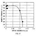
- Fig. 17 shows the correlation between surface roughness and magnetic permeability, on which the abscissa represents the surface roughness Ra ( ⁇ m) of the substrate and the ordinate represents the magnetic permeability ⁇ (-) of the magnetic film.
- the thin film device was configured so that a substrate (silicon oxide), a magnetic film (cobalt zirconium tantalum alloy), and a conductive film (copper) were disposed vertically in the order named. Further, magnetic permeability was determined with a shield loop coil method.
- the present invention has been described taking the embodiment as example, it is to be understood that the present invention should not be limited to this embodiment but is susceptible of various changes and modifications.
- the configuration of the thin film device or the thin film inductor can be changed freely as long as the surface roughness of the substrate falls within the range expressed in the above-mentioned expressions (11) and (12), and operating performance can be ensured by ensuring the adhesion of the conductive film or the coil and the magnetic characteristic of the magnetic film.
- the present invention may be applied to other devices other than the thin film inductor.
- the “other devices” are thin film transformers, thin film sensors, thin film resistors, thin film actuators, thin film magnetic heads, or MEMS, as described above.
- the applications of the thin film device of the present invention to these other devices also provide the same effect as in the foregoing embodiment.
Abstract
Description
- The present invention relates to a thin film device with a conductive film and a magnetic film each being layered on a substrate, and a thin film inductor with a coil and a magnetic film each being layered on a substrate.
- Recently, in the field of devices for various purposes, a thin film device with a conductive film and a magnetic film each being layered on a substrate is widely used. As an example of this thin film device, there is a thin film inductor having a coil for generating inductance as the above-mentioned conductive film. This thin film inductor has a structure including mainly a coil filled in with an insulating film , and a magnetic film, the coil and the magnetic film being layered on a substrate.
- In order to ensure the operating performance of thin film devices, it is necessary to ensure both of the adhesion property of the conductive film and the magnetic characteristic of the magnetic film. Considering the recent technical trend that there is the widening demand for improved operating performance of the thin film devices, it seems necessary to optimize not only the configurations of the conductive film and the magnetic film, but also the configuration of the substrate.
- Several techniques of ensuring the operating performance of the thin film devices have already been proposed. Specifically, there is known the technique of forming a coil by plating on a substrate (a ferrite substrate) having a surface roughness (an arithmetic mean roughness Ra) of 0.003 µm to 0.6 µm, in order to achieve miniaturization, high efficiency, and high output of a thin film inductor (refer to, for example,
Japanese Unexamined Patent Publication No. 11-168010 Japanese Unexamined Patent Publication No. 05-117838 - As described above, it is essential to ensuring of the operating performance of the thin film device that both of adhesion and magnetic characteristic be ensured. Nevertheless, in the thin film devices of the related art, adhesion and magnetic characteristic are not completely satisfactory, and hence there is much room for improvement. Particularly, in order to ensure the operating performance of the thin film device, not only to ensure adhesion and magnetic characteristic, but also to enable the thin film device to be stably manufactured is important.
- In view of the foregoing, it is desirable to provide a thin film device capable of ensuring operating performance by ensuring the adhesion of a conductive film and the magnetic characteristic of a magnetic film.
- It is also desirable to provide a thin film inductor capable of ensuring operating performance by ensuring the adhesion of a coil and the magnetic characteristic of a magnetic film.
- According to an embodiment of the present invention, there is provided a thin film device with a conductive film and a magnetic film each being layered on a substrate having a surface roughness within a range expressed in the following expression (1) and expression (2):


where Ra is a surface roughness (an arithmetic mean roughness (µm)) of the substrate; σ is an internal stress (MPa) of the conductive film; T is a thickness (µm) of the conductive film; W is a peak-to-peak pitch (µm) of irregularities providing that concaves and convexes are uniformly formed on a surface of the substrate; and P is adhesiveness (MPa) per unit length of the conductive film. - The term 'substrate' means all kinds of base materials (or base members) which are able to support some film structure formed thereon, specifically including bare substrate with no modification as well as composite substrate and modified substrate (or reformed substrate), where the composite substrate is a composition of bare substrate and some structure formed thereon, the structure including other bare substrate and/or a film formed of one or more layers, and the modified substrate is a bare substrate whose surface has been subjected to some modification process.
- In this thin film device, the surface roughness of the substrate is within the range expressed in the expression (1) and the expression (2). Consequently, an anchor effect can be used to ensure the adhesion of the conductive film, and magnetic characteristic (magnetic permeability) can also be ensured even if a magnetic film is provided on a substrate having a rough surface.
- Preferably, the surface roughness of the substrate lies within a range expressed in the following expression (3):


- Particularly, the conductive film may have a seed film and a plated film in that order from the substrate, the plated film being grown with use of the seed film.
- According to an other embodiment of the present invention, there is provided a thin film inductor with a coil and a magnetic film each being layered on a substrate having a surface roughness within a range expressed in the following expression (5) and expression (6):


where Ra is a surface roughness (an arithmetic mean roughness (µm)) of the substrate; σ is an internal stress (MPa) of the coil; T is a thickness (µm) of the coil; W is a peak-to-peak pitch (µm) of irregularities providing concaves and convexes are uniformly formed on a surface of the substrate; and P is adhesiveness (MPa) per unit length of the coil. - In this thin film inductor, the surface roughness of the substrate is within the range expressed in the expression (5) and the expression (6). Like the above-mentioned thin film device, the adhesion of the coil can be ensured and the magnetic characteristic (magnetic permeability) of the magnetic film can also be ensured.
- In the thin film device in accordance with the present invention, the substrate has a surface roughness within the range expressed in the expression (1) and the expression (2). Therefore, by ensuring the adhesion of the conductive film and the magnetic characteristic of the magnetic film, operating performance can be obtained.
- In the thin film inductor in accordance with the present invention, the substrate has a surface roughness within the range expressed in the expression (5) and the expression (6). Hence, the adhesion property of the coil and the magnetic characteristic of the magnetic film can be ensured, enabling operating performance to be ensured.
- Other and further objects, features and advantages of the invention will appear more fully from the following description.
-
- Fig. 1 is a sectional view showing the cross-sectional configuration of a thin film device according to an embodiment of the present invention;
- Fig. 2 is a sectional view showing in enlarged dimension a part of the thin film device shown in Fig. 1;
- Fig. 3 is a sectional view for explaining the principle of calculating the lower limit of the surface roughness of a substrate;
- Fig. 4 is a sectional view showing an example of the configuration of a conductive film;
- Fig. 5 is a sectional view for explaining the step of forming the conductive film shown in Fig. 4;
- Fig. 6 is a sectional view showing the step subsequent to that of Fig. 5;
- Fig. 7 is a sectional view showing an example of modifications related to the configuration of the thin film device according to an embodiment of the present invention;
- Fig. 8 is a sectional view showing another example of the modifications related to the configuration of the thin film device according to an embodiment of the present invention;
- Fig. 9 is a plan view showing the plan structure of a thin film inductor in the embodiment of the present invention;
- Fig. 10 is a sectional view showing a cross-sectional configuration taken along the line X-X of the thin film inductor shown in Fig. 9;
- Fig. 11 is a sectional view showing an example of the configuration of a coil;
- Fig. 12 is a sectional view showing an example of modifications of the thin film inductor in the embodiment of the present invention;
- Fig. 13 is a plan view showing the plan structure of a thin film inductor in another embodiment of the present invention;
- Fig. 14 is a sectional view showing a cross-sectional configuration taken along the line XIV-XIV of the thin film inductor shown in Fig. 13;
- Fig. 15 is a sectional view showing a cross-sectional configuration taken along the line XV-XV of the thin film inductor shown in Fig. 13;
- Fig. 16 is a sectional view showing a cross-sectional configuration taken along the line XVI-XVI of the thin film inductor shown in Fig. 13; and
- Fig. 17 is a diagram showing the correlation between surface roughness and magnetic permeability.
- Preferred embodiments of the present invention will now be described in detail with reference to the accompanying drawings.
- Reference to Figs. 1 and 2, the structure of a thin film device according to an embodiment of the present invention will be described as follows. Fig. 1 shows the cross-sectional configuration of a
thin film device 10. Fig. 2 shows in enlarged dimension a site (a site P1) of thethin film device 10 shown in Fig. 1. - The
thin film device 10 of this is to be used in the field of devices for various purposes and applied to, for embodiment example, thin film inductors, thin film transformers, thin film sensors, thin film actuators, thin film magnetic heads, or MEMS (micro electro mechanical systems). - The
thin film device 10 is constructed of aconductive film 2 and amagnetic film 3 each being layered on asubstrate 1, as shown in Fig. 1. The detailed configuration of thethin film device 10 can be determined freely as long as theconductive film 2 and themagnetic film 3 are layered on thesubstrate 1. That is, the layer configuration (monolayer or multilayer) of theconductive film 2, the layer configuration (monolayer or multilayer) of themagnetic film 3, and the laminate configuration (the order of layering) of theconductive film 2 and themagnetic film 3 can be set suitably depending on the condition, such as the application of thethin film device 10. Alternatively, thethin film device 10 may have other element (not shown), in addition to the above-mentionedconductive film 2 and themagnetic film 3. Examples of the "other element" are an insulating film electrically isolating between thesubstrate 1 and theconductive film 2, an insulating film electrically isolating theconductive film 2 from its surroundings, and an insulating film electrically isolating between theconductive film 2 and themagnetic film 3. - Here, the
thin film device 10 has, for example, the structure including theconductive film 2 of monolayer, and themagnetic film 3 of monolayer, each being layered in this order on thesubstrate 1. - The
substrate 1 may be any kind of base materials (or base members) which are able to support some film structure formed thereon, specifically including bare substrate with no modification as well as composite substrate and modified substrate (or reformed substrate), where the composite substrate is a composition of bare substrate and some structure formed thereon, the structure including other bare substrate and/or a film formed of one or more layers, and the modified substrate is a bare substrate whose surface has been subjected to some modification process. - The
conductive film 2 is a functional film performing various functions by using electrical conduction. For example, theconductive film 2 is constructed of a conductive material represented by various metals. The three dimensional structure of theconductive film 2 can be set freely depending on the various functions. For example, theconductive film 2 may have a flat structure when it functions as an electrode, or a winding structure when it works as a coil for generating inductance. The winding structure may, for example, be a spiral structure or solenoid structure, but is not limited in such structures. Figs. 1 and 2 show the case where theconductive film 2 has the flat structure, for example. - The
magnetic film 3 is a functional film performing various functions by using magnetism. For example, themagnetic film 3 is constructed of a magnetic material represented by various alloys. - As shown in Fig. 2, when the
thin film device 10 is viewed microscopically, theconductive film 2 is formed so as to cover thesubstrate 1 having surface roughness. Consequently, theconductive film 2 has a rough surface caused by the surface roughness of thesubstrate 1, and themagnetic film 3 is formed so as to cover theconductive film 2 having the rough surface. - Particularly, in the
thin film device 10, thesubstrate 1 has a certain surface roughness. The term "surface roughness" indicates a so-called arithmetic mean roughness Ra, and it is within the range expressed in the following expression (11) and expression (12). The principle of calculating the lower limit X of the surface roughness Ra expressed in the expression (11) and the expression (12) will be described later.

where Ra is a surface roughness (µm) of thesubstrate 1; σ is an internal stress (MPa) of theconductive film 2; T is a thickness (µm) of theconductive film 2; W is a width (µm) of irregularities providing concaves and convexes are uniformly formed on a surface of thesubstrate 1; and P is adhesiveness (MPa) per unit length of theconductive film 2. - The reason why the surface roughness Ra is preferable to be equal or more than X[µm] in the expression (12), namely (Ra ≧ X µm), is to enable ensuring of the adhesion of the
conductive film 2. As used herein, "the adhesion of theconductive film 2" depending on the surface roughness Ra means the adhesion to thesubstrate 1 as the base, namely adhesion utilizing a so-called anchor effect. As described previously, "the adhesiveness P per unit length of theconductive film 2" means adhesion utilizing no anchor effect, and it can simply be determined based on characteristic matching between materials. - On the other hand, the reason why it is preferable that the surface roughness Ra be within the range of 0.1 µm or less (Ra ≦ 0.1 µm) is to enable ensuring of the magnetic characteristic (the magnetic permeability µ) of the
magnetic film 3 even if themagnetic film 3 is provided on thesubstrate 1 having the surface irregular structure. - The mechanism that the surface roughness Ra influences on the magnetic characteristic of the
magnetic film 3 is as follows. That is, when a magnetic filed is applied in a direction parallel with the film surface of themagnetic film 3, the magnetization of themagnetic film 3 is reversed. The reversal of magnetization is caused based on the phenomenon that by applying the magnetic field to themagnetic film 3, energy is supplied to a magnetic spin and the magnetic spin is reversed with this energy. The degree of tendency of the magnetization reversal is so-called magnetic permeability µ. The magnetic permeability µ will be lowered due to disturbance of the reversal of magnetization by the presence of impurities, crystal defect, and the like. The magnetic permeability µ will also be lowered due to disturbance of the magnetic domain structure in themagnetic film 3 by the presence of a large surface irregularity (large surface roughness Ra) of the base. Hence, the surface roughness Ra of thesubstrate 1 can exert an adverse effect upon the magnetic characteristic of themagnetic film 3. More particularly, when the surface roughness Ra is too large, the magnetic characteristic is deteriorated due to a reduction in the magnetic permeability µ. - For purposes of confirmation, in the case as shown in Fig. 2, the
conductive film 2 directly adheres to thesubstrate 1, and hence the adhesion of theconductive film 2 means the adhesion to thesubstrate 1, and the adhesiveness P means the adhesiveness of theconductive film 2 to thesubstrate 1. On the other hand, in the case where the above-mentioned insulating film (not shown) as the other element is interposed between thesubstrate 1 and theconductive film 2, and theconductive film 2 indirectly adheres to thesubstrate 1 with the insulating film in between, the adhesion of theconductive film 2 means substantially the adhesion to the insulating film, and the adhesiveness P means the adhesiveness of theconductive film 2 to the insulating film. - Preferably, the surface roughness Ra is, for example, within the range expressed in the following expression (13):

- When the surface roughness Ra is 0.075 µm or less, the
magnetic film 3 is capable of achieving a magnetic permeability µ of the equivalent or more of the magnetic permeability µ when the surface roughness Ra is almost zero (the adverse effect due to the surface roughness Ra is negligibly small). - Preferably, the surface roughness Ra is, for example, within the range expressed in the following expression (14):

- When the surface roughness Ra is 0.004 µm or more, the adhesion of the
conductive film 2 can be ensured when the internal stress σ, the thickness T, the width W, and the adhesiveness P are set in a practical range, as will be described later. - If the surface roughness Ra of the
substrate 1 prepared for configuring thethin film device 10 is not in the range as shown in the expression (11) and the expression (12), the surface roughness Ra can be adjusted so as to fall within a suitable range by treatment of the substrate in various ways. As an example, if a silicon substrate (a so-called silicon wafer) or the like having a considerably small surface roughness Ra is used as thesubstrate 1, the surface roughness Ra can be increased into a suitable range by intentionally roughing the surface of thesubstrate 1 by using processing techniques represented by dry etching, sandblast, or ion milling. - Reference to Figs. 1 to 3, the principle of calculating the lower limit X of the surface roughness Ra expressed in the expression (12) will be described as follows. Fig. 3 is to explain the principle of calculating the lower limit of the surface roughness Ra of the
substrate 1, illustrating in enlarged dimension the surface irregular structure of thesubstrate 1. - The lower limit X of the surface roughness Ra is a threshold value to be defined from the point of view of ensuring the adhesion of the
conductive film 2, as described above, and it can be calculated by considering thethin film device 10 in Figs. 1 and 2, as a two-dimensional model. - Specifically, when a series of parameters of the surface roughness Ra (µm) of the
substrate 1, the internal stress σ (MPa) of theconductive film 2, the thickness T (µm) of theconductive film 2, and the adhesiveness P (MPa) per unit length of theconductive film 2 are set to thethin film device 10, as shown in Fig. 2, a shear stress F1 (MPa · µm) exerted on the interface between thesubstrate 1 and theconductive film 2 can be expressed in the following expression (21):
- Here, the internal stress σ may be considered to be concentrated at a site (a site P2) having a length of about 1 µm in the vicinity of one end of the
conductive film 2. This is because a partial delaminating of theconductive film 2 from thesubstrate 1, originating from the site P2 in the vicinity of the one end, may be considered to cause the whole of theconductive film 2 to start peeling from thesubstrate 1. As used herein, the term "length" means a dimension in a lateral direction as viewed in Fig. 2. - When the
conductive film 2 is in contact with thesubstrate 1 having the rough surface, the junction length (the effective junction length) of theconductive film 2 is greater than that when theconductive film 2 is in contact with theflat substrate 1, so that the adhesiveness (the effective adhesiveness) is increased. The effective adhesiveness per unit length of theconductive film 2, namely F2 (MPa · µm), can be expressed in the following expression (22):
where L (µm) is an effective junction length per unit length of theconductive film 2. - From these two expressions (21) and (22), the condition under which the
conductive film 2 does not delaminated from thesubstrate 1 can be expressed in the following expression (23), and hence it can substantially be expressed in the following expression (24).

- This effective junction length L satisfies the correlation expressed in the following expression (25):

where f(x) is a function related to the surface irregular structure of thesubstrate 1, namely a function indicating a height from a specific reference surface. - At this time, the surface roughness Ra satisfies the correlation expressed in the following expression (26):

where the surface roughness Ra can be obtained by extracting from a roughness curve by a reference length D in a direction of an average line of the roughness curve, and summing and then averaging the absolute values of deviation from the average line of the extracted portion to a measured curve. - By specifying the surface roughness Ra from these two expressions (25) and (26), the effective junction length L can be calculated. The surface roughness Ra and the effective junction length L can also be actually measured with a contact unevenness meter or the like.
- Here, it is assumed that the surface of the
substrate 1 is uniformly provided with irregularities (or pebbling), as shown in Fig. 3. Then, when the width of the irregularities is W (µm), and the height of the irregularities is H (µm), there are present 1/W pieces of irregularities per unit width (1 µm in width). As used herein, the term "the width of irregularities" is a so-called pitch of irregularities (a distance between concave portions or a distance between convex portions), and the term "the height of irregularities" is a so-called height of the convex portions. The effective junction length L in this case can be expressed in the following expression (27). Particularly, when the surface of thesubstrate 1 is uniformly provided with the concaves and convexes, the surface roughness Ra can be expressed in the following expression (28). Therefore, from these two expressions (27) and (28), the effective junction length L can be expressed in the following expression (29).


- Accordingly, by introducing the expression (29), the above-mentioned expression (24) can be expressed in the following expression (30):

- By changing the expression (30), the surface roughness Ra, namely a threshold value to be defined from the point of view of ensuring the adhesion of the
conductive film 2, can be expressed in the following expression (31):
- This enables to calculate the lower limit X (=Ra) of the surface roughness Ra expressed in the expression (12).
- As an example of specific ranges of the surface roughness Ra, in the case where, as the configuration of a practical
thin film device 10, the substrate 1 (silicon oxide (typically SiO2)) and the conductive film 2 (copper (Cu)) are included under the conditions of 27.8 MPa in internal stressσ, 20 µm in thickness T, 0.1 µm in width W, and 270 MPa in adhesiveness P, the fact that the surface roughness Ra is necessary to satisfy the expression: 0.004 µm ≦ Ra ≦ 0.1 µm, can be found from the above-mentioned expressions (11) and (12). - In the thin film device of this embodiment, the surface roughness Ra of the
substrate 1 is within the range as expressed in the expressions (11) and (12). This enables to optimize the surface roughness Ra of thesubstrate 1 from the point of view of ensuring both of the adhesion of theconductive film 2 and the magnetic characteristic (the magnetic permeability) of themagnetic film 3, as discussed above. Hence, ensuring the adhesion of theconductive film 2 and the magnetic characteristic of themagnetic film 3 can ensure the operating performance. - In particular, the present embodiment is capable of further improving the magnetic characteristic of the
magnetic film 3, if the surface roughness Ra falls within the range expressed in the expression (13). - The present embodiment is also capable of ensuring the adhesion of the
conductive film 2 when the internal stress σ, the thickness T, the width W, and the adhesiveness P are set in a practical range, if the surface roughness Ra falls within the range expressed in the expression (14). - Description will now be made of the technical significance of the present invention. That is, in order to ensure the operating performance of the
thin film device 10 by ensuring both of the adhesion of theconductive film 2 and the magnetic characteristic of themagnetic film 3, the present invention defines a proper range of the surface roughness Ra of thesubstrate 1, as shown in the expressions (11) and (12). With regard to the surface roughness Ra, the above-mentioned publication (Japanese Unexamined Patent Publication No. 11-168010 - In the present embodiment, the configuration (the forming method) of the
conductive film 2 can be set freely. For example, as shown in Fig. 4 corresponding to Fig. 1, by forming theconductive film 2 with an electro-plating method, theconductive film 2 may be configured so as to have aseed film 2A, and a platedfilm 2B grown with use of theseed layer 2A, theseed film 2A being closer to thesubstrate 1 than theplate film 2B. In this case, the adhesiveness P per unit length of theconductive film 2 is the adhesiveness per unit length of theseed layer 2A. The material constituting theseed layer 2A may be identical with or different from that of the platedfilm 2B. - The
conductive film 2 can be formed through the procedure, for example, as shown in Figs. 5 and 6 corresponding to Fig. 4. That is, when forming aconductive film 2, as shown in Fig. 5, aseed film 2A is firstly formed so as to cover thesubstrate 1, and then a platedfilm 2B is formed in a pattern by electro plating with use of theseed layer 2A. In this case, for example, a photoresist pattern (not shown) is used to selectively grow the platedfilm 2B, and the used photoresist pattern is then removed. Subsequently, as shown in Fig. 6, the unnecessary portions of theseed film 2A are etched away by wet etching or the like. This results in theconductive film 2 having theseed film 2A and the platedfilm 2B. - Even if the
conductive film 2 is configured as described with reference to Figs. 4 to 6, the same effect as in the foregoing embodiment can be obtained. Otherwise, the configuration of thethin film device 10 shown in Fig. 4 is identical to that shown in Fig. 1. - Particularly, in the case as shown in Figs. 4 to 6, the
thin film device 10 can be manufactured stably from the point of view of manufacturing process, for the reason as follows. That is, as shown in Fig. 5 and 6, when the unnecessary portions of theseed film 2A are etched away by wet etching, if the surface roughness Ra is beyond the range expressed in the expression (11), (Ra>0.1 µm), the surface irregularities of thesubstrate 1 is too large. Therefore, an etchant is hard to reach fine portions (vacancies (deeply recessed portions)). As a result, poor etching is liable to occur, making it difficult to stably manufacture thethin film device 10. In contrast, in the present embodiment, because the surface roughness Ra falls within the range expressed in the expression (11), (Ra≦0.1 µm), the surface irregularities of thesubstrate 1 is not too large. Therefore, an etchant is easy to reach the fine portions. This suppresses poor etching and permits stable manufacturing of thethin film device 10. - Although in the present embodiment, the
thin film device 10 is configured so as to have the laminate structure that theconductive film 2 and themagnetic film 3 are layered in this order on thesubstrate 1, as shown in Fig. 1, the configuration of thethin film device 10 is not limited to this, and it can be set suitably depending on the condition such as use and the like, as described above. As a specific example, thethin film device 10 may be configured so as to have a laminate structure including themagnetic film 3 and theconductive film 2 layered in this order on thesubstrate 1, as shown in Fig. 7 corresponding to Fig. 1. Alternatively, thethin film device 10 may be configured so as to have a laminate structure including themagnetic film 3, theconductive film 2, and themagnetic film 3, which are layered in this order on thesubstrate 1, in other words, theconductive film 2 is interposed between the twomagnetic films 3. These two alternatives also provide the same effect as the forgoing embodiment. Otherwise, the configurations of thethin film devices 10 shown in Figs. 7 and 8, respectively, are identical to that shown in Fig. 1. - This completes the description of the thin film device according to the embodiment of the present invention.
- Description will next be made of an example of applications of the above-mentioned thin film device. In the following, Fig. 1 referred to describe the
thin film device 10 will be referred to whenever it is necessary. - Figs. 9 and 10 show the configuration of a
thin film inductor 100 to which applied is the thin film device 10 (refer to Fig. 1); Fig. 9 shows its plan configuration; and Fig. 10 shows a cross-sectional configuration taken along the line X-X in Fig. 9. - As shown in Figs. 9 and 10, for example, the
thin film inductor 100 can be constructed of a lowermagnetic film 12 and an uppermagnetic film 17 deposited on asubstrate 11 in this order in a direction away from thesubstrate 11, and acoil 16 deposited between the lowermagnetic film 12 and the uppermagnetic film 17. For example, thecoil 16 is filled in with an insulatingfilm 20 disposed between the uppermagnetic film 12 and the lowermagnetic film 17. In other words, thethin film inductor 100 has the structure that the lowermagnetic film 12, thecoil 16 filled in with the insulatingfilm 20, and the uppermagnetic film 17 are layered in this order on thesubstrate 11. - The
substrate 11 corresponds to the substrate 1 (refer to Fig. 1), and has a surface roughness Ra expressed in the expressions (11) and (12). For example, thesubstrate 11 may be selected from various substrates of glass, silicon (Si), silicon oxide, aluminium oxide (Al2O3, being so-called alumina), ceramic, a semiconductor, or a resin, and these various substrates with various functional films. It should be understood that the material constituting thesubstrate 11 is not limited to the above-mentioned materials. In fact, one could use any other material. - Especially, in order to improve the magnetic characteristic of the
thin film inductor 100, it is preferable that thesubstrate 11 be a magnetic substrate such as a ferrite substrate. Particularly, a ferrite substrate of nickel copper zinc alloy (NiCuZn) having an insulating property is suitable because it enables to directly form thecoil 16 on thesubstrate 11, for the purpose of simplifying the configuration and omitting some of the manufacturing process of thethin film inductor 100. - The lower
magnetic film 12 and the uppermagnetic film 17 correspond to the magnetic film 3 (refer to Fig. 1), respectively, and have a function of enhancing inductance. The lowermagnetic film 12 and the uppermagnetic film 17 are constructed of, for example, a magnetic material represented by a cobalt (Co) alloy or an iron (Fe) alloy. As an example of cobalt alloys, there is a cobalt zirconium tantalum alloy (CoZrTa), a cobalt zirconium niobium alloy (CoZrNb), or the like. As an example of iron alloys, there is a cobalt iron alloy (CoFe) or the like. - The insulating
film 20 electrically isolates thecoil 16 from its surroundings. For example, the insulatingfilm 20 has a three-layer structure that a lower insulatingfilm 13 supporting thecoil 16, an intermediate insulatingfilm 14 filling in between the windings of thecoil 16 and its surroundings, and an upper insulatingfilm 15 covering thecoil 16 are layered in this order in a direction away from the lowermagnetic film 12. The lower insulatingfilm 13, the intermediate insulatingfilm 14, and the upper insulatingfilm 15 are respectively constructed of an insulating material such as silicon oxide. The configuration of the insulatingfilm 20 is not limited to the above-mentioned three-layer structure, and it can be changed freely. - The
coil 16 corresponds to the conductive film 2 (refer to Fig. 1), and is constructed of a conductive material represented by metal, such as copper, nickel (Ni), or silver (Ag). For example, thecoil 16 has a spiral structure that one end (a terminal 16E1) and the other end (a terminal 16E2) are led out to the outside of the insulatingfilm 20, so as to generate inductance between these two terminals 16E1 and 16E2. The adhesiveness P expressed in the above-mentioned expression (12), namely an adhesiveness P per unit length of thecoil 16 corresponding to theconductive film 2, is substantially an adhesiveness to the insulating film 20 (the lower insulating film 13). - In the
thin film inductor 100, the surface roughness Ra of thesubstrate 11 is within the range expressed in the expressions (11) and (12). Therefore, by the same mechanism as thethin film device 10, the adhesion of thecoil 16 can be ensured, and the magnetic characteristic (the magnetic permeability) of the lowermagnetic film 12 and the uppermagnetic film 17 can also be ensured. This enables to ensure operating performance. - In this case, especially, the magnetic path of the
thin film inductor 100 become closer to a closed magnetic path because thecoil 16 is interposed between the lowermagnetic film 12 and the uppermagnetic film 17. It is therefore possible to improve magnetic characteristic more than the case where only the lowermagnetic film 12 is provided without having the uppermagnetic film 17, as shown in Fig. 12 to be described later. - Of course, in the
thin film inductor 100, thecoil 16 may be configured so as to include aseed layer 16A and a plated film 16B as shown in Fig. 11 corresponding to Fig. 10, by applying the configuration example of theconductive film 2 as described with reference to Fig. 4. In this case, thethin film inductor 100 can be manufactured stably by the same mechanism as thethin film device 10 in the foregoing description. Otherwise, the configuration of thethin film inductor 100 shown in Fig. 11 is identical to that shown in Fig. 10. - Alternatively, the
thin film device 100 may be configured so as to have only the lowermagnetic film 12 without having the uppermagnetic film 17, as shown in Fig. 12 corresponding to Fig. 10. This also ensures operating performance as in the case shown in Fig. 10. Otherwise, the configuration of thethin film inductor 100 shown in Fig. 12 is identical to that shown in Fig. 10. - The configuration, the action, and the effect of the
thin film inductor 100 other than those described above are identical to those in the above-mentionedthin film device 10, and therefore the descriptions thereof are omitted. - Figs. 13 to 16 show the configuration of a
thin film inductor 200 to which applied is thethin film device 10; Fig. 13 shows its plan configuration; and Figs. 14 to 16 show cross-sectional configurations, respectively. More specifically, Figs. 14 to 16 show the cross-sectional configurations taken along the line VIV-VIV, the line XV-XV, and the line XVI -XVI in Fig. 13, respectively. - As shown in Figs. 13 to 16, the
thin film inductor 200 has the configuration that a lowermagnetic film 22, and an uppermagnetic film 23 and acoil 24 each being filled in with an insulatingfilm 25, are layered on asubstrate 21. The lowermagnetic film 22 and the uppermagnetic film 23 are opposed to each other, and thecoil 24 has a solenoid type structure wound around the uppermagnetic film 23. - The
substrate 21 corresponds to the substrate 1 (refer to Fig. 1), and has a surface roughness Ra expressed in the expressions (11) and (12). For example, thesubstrate 21 is constructed of the same material as thesubstrate 11 in the above-mentionedthin film inductor 100. - The lower
magnetic film 22 and the uppermagnetic film 23 correspond to the magnetic film 3 (refer to Fig. 1), respectively, and have a function of enhancing inductance. For example, the lowermagnetic film 22 and the uppermagnetic film 23 are constructed of the same magnetic material as in the lowermagnetic film 12 and the uppermagnetic film 17 in the above-mentionedthin film inductor 100, or a conductive magnetic material such as a nickel iron alloy (NiFe). - The
coil 24 corresponds to the conductive film 2 (refer to Fig. 1), and is constructed of a conductive material such as copper. Thecoil 24 generates inductance in between one end (a terminal 24T1) and the other end (a terminal 24T2), and the terminal 24T1 and the terminal 24T2 are led out to the outside of the insulatingfilm 25. - The
coil 24 includes a plurality of strip lower andupper coil portions intermediate coil portions 24C, each portion being connected in series. Thelower coil portions 24A are arranged in a layer (a lower layer) between the lowermagnetic film 22 and the uppermagnetic film 23. Theupper coil portions 24B are arranged in a layer (an upper layer) on the opposite side of thelower coil portions 24A with the uppermagnetic film 23 interposed in between, so as to be overlapped with one end or the other end of thelower coil portions 24A. For example, these lower andupper coil portions intermediate coil portions 24C are arranged at a layer between the lower layer and the upper layer, at which thelower coil portions 24A and theupper coil portions 24B are overlapped with each other. Here, the adhesiveness P expressed in the above-mentioned expression (12), namely an adhesiveness P per unit length of the coil 24 (thelower coil portions 24A and theupper coil portions 24B) corresponding to theconductive film 2, is substantially an adhesiveness P to the insulating film 25 (a lower insulatingfilm 25A and an upperinsulating film 25C). - The number of turns of the
coil 24 can be set arbitrarily. In Figs. 13 to 16, there are shown, for example, the case where the number of turns of thecoil 24 is four turns. In this case, for example, the use of thelower coil portions 24A as the terminals 24T1 and 24T2 allows fivelower coil portions 24A (24A1 to 24A5) and fourupper coil portions 24B (24B1 to 24B4) to be arranged. - The thickness TA of the lower coil portions 14A and the thickness TB of the upper coil portions 14B can be set arbitrarily. In Figs. 14 to 16, there are shown, for example, the case where the thickness TA and the thickness TB are identical.
- The insulating
film 25 electrically isolates thecoil 24 from the lowermagnetic film 22 and the uppermagnetic film 23, and it is constructed of, for example, an insulating non-magnetic material such as silicon oxide, or an insulating resin material such as polyimide or resist. For example, the insulatingfilm 25 includes a lower insulatingfilm 25A deposited on the lowermagnetic film 22, a lowercoil insulating film 25B disposed on the lower insulatingfilm 25A so as to fill in thelower coil portions 24A, an upperinsulating film 25C disposed on the lowercoil insulating film 25B so as to fill in the uppermagnetic film 23, an uppercoil insulating film 25D disposed on the upper insulatingfilm 25C so as to fill in theupper coil portions 24B. In the lowercoil insulating film 25B and the upper insulatingfilm 25C, contact holes 25H are provided for each position where thelower coil portion 24A and theupper coil portion 24B are overlapped with each other. Theintermediate coil portions 24C are buried in the contact holes 25H, respectively. The materials constituting a series of the insulatingfilms 25A to 25D are not necessarily identical, and they may be set individually. - In the
thin film inductor 200, the surface roughness Ra of thesubstrate 21 is within the range expressed in the expressions (11) and (12). Therefore, by the same action as thethin film device 10, the adhesion of thecoil 24 can be ensured, and the magnetic characteristic (the magnetic permeability) of the lowermagnetic film 22 and the uppermagnetic film 23 can also be ensured. This enables to ensure operating performance. Otherwise, the effect and modifications of thethin film inductor 200 are identical to those of the above-mentionedthin film inductor 100. - Examples of the present invention will be described below.
- The magnetic characteristic of the thin film device described with reference to Fig. 7 in the foregoing embodiment was examined to obtain the results as presented in Fig. 17. Fig. 17 shows the correlation between surface roughness and magnetic permeability, on which the abscissa represents the surface roughness Ra (µm) of the substrate and the ordinate represents the magnetic permeability µ (-) of the magnetic film. In order to examine the magnetic characteristic, the thin film device was configured so that a substrate (silicon oxide), a magnetic film (cobalt zirconium tantalum alloy), and a conductive film (copper) were disposed vertically in the order named. Further, magnetic permeability was determined with a shield loop coil method.
- As can be seen from the results presented in Fig. 17, the magnetic permeability µ became almost constant and was then lowered as the surface roughness Ra was increased. More specifically, the magnetic permeability µ was almost constant in the initial stage (Ra = 0.002 µm to 0.075 µm), and was lowered gently in the middle stage (Ra = 0.075 µm to 0.1 µm), and then lowered rapidly in the latter stage (Ra = 0.1 µm to 0.12 µm). This proves that in the thin film device of the present invention, the magnetic permeability µ can be ensured when the surface roughness Ra is within the range of 0.1 µm or less (Ra≦0.1 µm). This also proves that the magnetic permeability µ of the equivalent or more of the magnetic permeability µ when the surface roughness Ra is almost zero can be obtained especially when the surface roughness Ra is within the range of 0.075 µm or less (Ra≦0.075 µm).
- While the present invention has been described taking the embodiment as example, it is to be understood that the present invention should not be limited to this embodiment but is susceptible of various changes and modifications. Specifically, the configuration of the thin film device or the thin film inductor can be changed freely as long as the surface roughness of the substrate falls within the range expressed in the above-mentioned expressions (11) and (12), and operating performance can be ensured by ensuring the adhesion of the conductive film or the coil and the magnetic characteristic of the magnetic film.
- Although the foregoing embodiment has discussed the case where the thin film device of the present invention is applied to the thin film inductor, without limiting to this, the present invention may be applied to other devices other than the thin film inductor. Examples of the "other devices" are thin film transformers, thin film sensors, thin film resistors, thin film actuators, thin film magnetic heads, or MEMS, as described above. The applications of the thin film device of the present invention to these other devices also provide the same effect as in the foregoing embodiment.
- It should be understood by those skilled in the art that various modifications, combinations, sub-combinations and alterations may occur depending on design requirements and other factors insofar as they are within the scope of the appended claims or the equivalents thereof.
Claims (5)
- A thin film device with a conductive film and a magnetic film each being layered on a substrate having a surface roughness within a range expressed in the following expression (1) and expression (2):

 σ is an internal stress (MPa) of the conductive film;T is a thickness (µm) of the conductive film;W is a peak-to-peak pitch (µm) of irregularities providing that concaves and convexes are uniformly formed on a surface of the substrate; andP is adhesiveness (MPa) per unit length of the conductive film.
 - The thin film device according to claim 1 wherein the surface roughness of the substrate lies in a range expressed in the following expression (3):

- The thin film device according to claim 1 wherein the surface roughness of the substrate lies in a range expressed in the following expression (4):

- The thin film device according to claim 1 wherein the conductive film includes a seed film and a plated film in that order from the substrate, the plated film being grown with use of the seed film.
- A thin film inductor with a coil and a magnetic film each being layered on a substrate having a surface roughness within a range expressed in the following expression (5) and expression (6):


where Ra is a surface roughness (an arithmetic mean roughness (µm)) of the substrate;σ is an internal stress (MPa) of the coil;T is a thickness (µm) of the coil;W is a peak-to-peak pitch (µm) of irregularities providing that concaves and convexes are uniformly formed on a surface of the substrate; andP is adhesiveness (MPa) per unit length of the coil.
Applications Claiming Priority (2)
| Application Number | Priority Date | Filing Date | Title |
|---|---|---|---|
| JP2005288434 | 2005-09-30 | ||
| JP2006267488A JP2007123866A (en) | 2005-09-30 | 2006-09-29 | Thin film device and thin-film inductor |
Publications (1)
| Publication Number | Publication Date |
|---|---|
| EP1783789A1 true EP1783789A1 (en) | 2007-05-09 |
Family
ID=37888235
Family Applications (1)
| Application Number | Title | Priority Date | Filing Date |
|---|---|---|---|
| EP06020617A Withdrawn EP1783789A1 (en) | 2005-09-30 | 2006-09-29 | Thin film device and thin film inductor |
Country Status (5)
| Country | Link |
|---|---|
| US (1) | US20070077395A1 (en) |
| EP (1) | EP1783789A1 (en) |
| JP (1) | JP2007123866A (en) |
| KR (1) | KR100827579B1 (en) |
| CN (1) | CN1967740A (en) |
Cited By (2)
| Publication number | Priority date | Publication date | Assignee | Title |
|---|---|---|---|---|
| KR100827579B1 (en) | 2005-09-30 | 2008-05-07 | 티디케이가부시기가이샤 | Thin film device and thin film inductor |
| US9709634B2 (en) | 2012-01-31 | 2017-07-18 | Osaka City University | Battery system and charge/discharge measuring apparatus |
Families Citing this family (10)
| Publication number | Priority date | Publication date | Assignee | Title |
|---|---|---|---|---|
| JP5194717B2 (en) * | 2007-10-31 | 2013-05-08 | 戸田工業株式会社 | Ferrite molded sheet, sintered ferrite substrate and antenna module |
| KR101187172B1 (en) | 2007-03-07 | 2012-09-28 | 도다 고교 가부시끼가이샤 | Ferrite Molded Sheet, Sintered Ferrite Substrate and Antenna Module |
| JP5082675B2 (en) * | 2007-08-23 | 2012-11-28 | ソニー株式会社 | Inductor and method of manufacturing inductor |
| JP5176989B2 (en) * | 2009-01-28 | 2013-04-03 | Tdk株式会社 | Common mode filter and its mounting structure |
| CN102299149A (en) * | 2010-06-23 | 2011-12-28 | 上海宏力半导体制造有限公司 | Semiconductor inductance device and manufacturing method thereof |
| KR20130072815A (en) * | 2011-12-22 | 2013-07-02 | 삼성전기주식회사 | Filter for removing noise and method of the same |
| US10015879B2 (en) * | 2016-01-27 | 2018-07-03 | Corning Incorporated | Silica content substrate such as for use harsh environment circuits and high frequency antennas |
| US9859357B1 (en) * | 2016-07-14 | 2018-01-02 | International Business Machines Corporation | Magnetic inductor stacks with multilayer isolation layers |
| CN108387784B (en) * | 2018-02-02 | 2020-11-20 | 上海交通大学 | Magnetic film inductive sensor |
| KR102333079B1 (en) * | 2019-12-09 | 2021-12-01 | 삼성전기주식회사 | Coil component |
Citations (8)
| Publication number | Priority date | Publication date | Assignee | Title |
|---|---|---|---|---|
| JPH05117838A (en) * | 1991-10-28 | 1993-05-14 | Power Reactor & Nuclear Fuel Dev Corp | Amorphous coating method |
| US5529831A (en) * | 1993-12-09 | 1996-06-25 | Alps Electric Co., Ltd. | Thin film device |
| JPH11168010A (en) * | 1997-12-04 | 1999-06-22 | Yamaha Corp | Microindutor |
| US20020105405A1 (en) * | 2000-01-28 | 2002-08-08 | Seung-Yun Lee | Method of fabricating silver inductor |
| US6661622B1 (en) * | 2000-07-17 | 2003-12-09 | International Business Machines Corporation | Method to achieve low and stable ferromagnetic coupling field |
| EP1467216A2 (en) * | 2003-02-25 | 2004-10-13 | Samsung Electronics Co., Ltd. | Method for manufacturing magnetic field detecting element |
| US20050052267A1 (en) * | 2003-07-25 | 2005-03-10 | Kyocera Corporation | Ferrite core, method of manufacturing the same, and common-mode noise filter using the same |
| US20060152321A1 (en) * | 2005-01-07 | 2006-07-13 | Samsung Electro-Mechanics Co., Ltd. | Planar magnetic inductor and method for manufacturing the same |
Family Cites Families (4)
| Publication number | Priority date | Publication date | Assignee | Title |
|---|---|---|---|---|
| JP3545074B2 (en) * | 1994-12-27 | 2004-07-21 | 独立行政法人 科学技術振興機構 | Magnetic detecting element and magnetic detecting module integrated on semiconductor substrate |
| KR100480749B1 (en) * | 1998-07-07 | 2005-09-30 | 삼성전자주식회사 | A differential solenoid magnetic |
| JP2004274004A (en) * | 2003-01-16 | 2004-09-30 | Fuji Electric Device Technology Co Ltd | Microminiature power converter |
| EP1783789A1 (en) | 2005-09-30 | 2007-05-09 | TDK Corporation | Thin film device and thin film inductor |
-
2006
- 2006-09-29 EP EP06020617A patent/EP1783789A1/en not_active Withdrawn
- 2006-09-29 JP JP2006267488A patent/JP2007123866A/en not_active Withdrawn
- 2006-09-30 CN CNA2006101437603A patent/CN1967740A/en active Pending
- 2006-10-02 US US11/540,670 patent/US20070077395A1/en not_active Abandoned
- 2006-10-02 KR KR1020060097403A patent/KR100827579B1/en not_active IP Right Cessation
Patent Citations (8)
| Publication number | Priority date | Publication date | Assignee | Title |
|---|---|---|---|---|
| JPH05117838A (en) * | 1991-10-28 | 1993-05-14 | Power Reactor & Nuclear Fuel Dev Corp | Amorphous coating method |
| US5529831A (en) * | 1993-12-09 | 1996-06-25 | Alps Electric Co., Ltd. | Thin film device |
| JPH11168010A (en) * | 1997-12-04 | 1999-06-22 | Yamaha Corp | Microindutor |
| US20020105405A1 (en) * | 2000-01-28 | 2002-08-08 | Seung-Yun Lee | Method of fabricating silver inductor |
| US6661622B1 (en) * | 2000-07-17 | 2003-12-09 | International Business Machines Corporation | Method to achieve low and stable ferromagnetic coupling field |
| EP1467216A2 (en) * | 2003-02-25 | 2004-10-13 | Samsung Electronics Co., Ltd. | Method for manufacturing magnetic field detecting element |
| US20050052267A1 (en) * | 2003-07-25 | 2005-03-10 | Kyocera Corporation | Ferrite core, method of manufacturing the same, and common-mode noise filter using the same |
| US20060152321A1 (en) * | 2005-01-07 | 2006-07-13 | Samsung Electro-Mechanics Co., Ltd. | Planar magnetic inductor and method for manufacturing the same |
Non-Patent Citations (1)
| Title |
|---|
| BRANDON E J ET AL: "PRINTED MICROINDUCTORS ON FLEXIBLE SUBSTRATES FOR POWER APPLICATIONS", IEEE TRANSACTIONS ON COMPONENTS AND PACKAGING TECHNOLOGIES, IEEE SERVICE CENTER, PISCATAWAY, NJ, US, vol. 26, no. 3, September 2003 (2003-09-01), pages 517 - 523, XP001192672, ISSN: 1521-3331 * |
Cited By (2)
| Publication number | Priority date | Publication date | Assignee | Title |
|---|---|---|---|---|
| KR100827579B1 (en) | 2005-09-30 | 2008-05-07 | 티디케이가부시기가이샤 | Thin film device and thin film inductor |
| US9709634B2 (en) | 2012-01-31 | 2017-07-18 | Osaka City University | Battery system and charge/discharge measuring apparatus |
Also Published As
| Publication number | Publication date |
|---|---|
| KR20070037428A (en) | 2007-04-04 |
| US20070077395A1 (en) | 2007-04-05 |
| CN1967740A (en) | 2007-05-23 |
| JP2007123866A (en) | 2007-05-17 |
| KR100827579B1 (en) | 2008-05-07 |
Similar Documents
| Publication | Publication Date | Title |
|---|---|---|
| EP1783789A1 (en) | Thin film device and thin film inductor | |
| EP0884783A2 (en) | A micromagnetic device for power processing applications and method of manufacture therefor | |
| US20140167898A1 (en) | Systems and methods for coupled power inductors | |
| EP3276365B1 (en) | A sensor device with a soft magnetic alloy having reduced coercivity, and method for making same | |
| US10937586B2 (en) | Electromagnetic device having layered magnetic material components and methods for making same | |
| JPH0916908A (en) | Thin-film magnetic core coil assembly | |
| JP4047115B2 (en) | Soft magnetic film, thin film magnetic head using the soft magnetic film, and method for manufacturing the soft magnetic film | |
| JP2007273802A (en) | Thin-film device | |
| JP5727908B2 (en) | Magnetic memory element | |
| TW319945B (en) | ||
| JP4998292B2 (en) | Magnetic thin film and thin film magnetic device | |
| JP2007273804A (en) | Thin-film device | |
| TW202131357A (en) | Nanomagnetic inductor cores, inductors and devices incorporating such cores, and associated manufacturing methods | |
| US20040080868A1 (en) | Electroplated magnetic thin film, method of manufacturing the same, electroplating bath and thin film magnetic head | |
| Flynn et al. | Characterization of core materials for microscale magnetic components operating in the megahertz frequency range | |
| JPH0529172A (en) | Manufacture of soft magnetic multilayer-plated film, said film and magnetic head | |
| CN114899000A (en) | Fluxgate sensor iron core and preparation method thereof | |
| CN114761816A (en) | Magnetic sensor and method for manufacturing magnetic sensor | |
| Coutrot et al. | Electromagnetic micro-device realized by electrochemical way | |
| JP2002050520A (en) | Microinductor or microelement or microtransformer type | |
| JPH08511378A (en) | Magnetoresistive device and magnetic head comprising such a device | |
| JP2535819B2 (en) | Method of manufacturing thin film magnetic head | |
| Ryu et al. | Characteristics of twin spiral type thin film inductor with Fe-based nanocrystalline core | |
| JPH10283618A (en) | Magneto-resistive film, memory element formed by using the same and their production | |
| JPS63283004A (en) | Flat surface inductor and manufacture thereof |
Legal Events
| Date | Code | Title | Description |
|---|---|---|---|
| PUAI | Public reference made under article 153(3) epc to a published international application that has entered the european phase |
Free format text: ORIGINAL CODE: 0009012 |
|
| AK | Designated contracting states |
Kind code of ref document: A1 Designated state(s): AT BE BG CH CY CZ DE DK EE ES FI FR GB GR HU IE IS IT LI LT LU LV MC NL PL PT RO SE SI SK TR |
|
| AX | Request for extension of the european patent |
Extension state: AL BA HR MK YU |
|
| 17P | Request for examination filed |
Effective date: 20071010 |
|
| 17Q | First examination report despatched |
Effective date: 20071112 |
|
| R17C | First examination report despatched (corrected) |
Effective date: 20071127 |
|
| AKX | Designation fees paid |
Designated state(s): AT BE BG CH CY CZ DE DK EE ES FI FR GB GR HU IE IS IT LI LT LU LV MC NL PL PT RO SE SI SK TR |
|
| STAA | Information on the status of an ep patent application or granted ep patent |
Free format text: STATUS: THE APPLICATION IS DEEMED TO BE WITHDRAWN |
|
| 18D | Application deemed to be withdrawn |
Effective date: 20090401 |