EP1788606A2 - Plasma Display Panel - Google Patents
Plasma Display Panel Download PDFInfo
- Publication number
- EP1788606A2 EP1788606A2 EP06124514A EP06124514A EP1788606A2 EP 1788606 A2 EP1788606 A2 EP 1788606A2 EP 06124514 A EP06124514 A EP 06124514A EP 06124514 A EP06124514 A EP 06124514A EP 1788606 A2 EP1788606 A2 EP 1788606A2
- Authority
- EP
- European Patent Office
- Prior art keywords
- light
- discharge
- pdp
- emitting layer
- discharge electrode
- Prior art date
- Legal status (The legal status is an assumption and is not a legal conclusion. Google has not performed a legal analysis and makes no representation as to the accuracy of the status listed.)
- Granted
Links
Images


Classifications
-
- H—ELECTRICITY
- H01—ELECTRIC ELEMENTS
- H01J—ELECTRIC DISCHARGE TUBES OR DISCHARGE LAMPS
- H01J11/00—Gas-filled discharge tubes with alternating current induction of the discharge, e.g. alternating current plasma display panels [AC-PDP]; Gas-filled discharge tubes without any main electrode inside the vessel; Gas-filled discharge tubes with at least one main electrode outside the vessel
- H01J11/10—AC-PDPs with at least one main electrode being out of contact with the plasma
- H01J11/12—AC-PDPs with at least one main electrode being out of contact with the plasma with main electrodes provided on both sides of the discharge space
-
- H—ELECTRICITY
- H01—ELECTRIC ELEMENTS
- H01J—ELECTRIC DISCHARGE TUBES OR DISCHARGE LAMPS
- H01J11/00—Gas-filled discharge tubes with alternating current induction of the discharge, e.g. alternating current plasma display panels [AC-PDP]; Gas-filled discharge tubes without any main electrode inside the vessel; Gas-filled discharge tubes with at least one main electrode outside the vessel
- H01J11/20—Constructional details
- H01J11/34—Vessels, containers or parts thereof, e.g. substrates
- H01J11/42—Fluorescent layers
-
- H—ELECTRICITY
- H01—ELECTRIC ELEMENTS
- H01J—ELECTRIC DISCHARGE TUBES OR DISCHARGE LAMPS
- H01J31/00—Cathode ray tubes; Electron beam tubes
- H01J31/08—Cathode ray tubes; Electron beam tubes having a screen on or from which an image or pattern is formed, picked up, converted, or stored
- H01J31/10—Image or pattern display tubes, i.e. having electrical input and optical output; Flying-spot tubes for scanning purposes
- H01J31/12—Image or pattern display tubes, i.e. having electrical input and optical output; Flying-spot tubes for scanning purposes with luminescent screen
Definitions
- the present invention relates to a Plasma Display Panel (PDP), and more particularly, the present invention relates to an opposed discharge PDP including an electroluminescent (EL) emitting layer.
- PDP Plasma Display Panel
- EL electroluminescent
- PDPs Plasma Display Panels
- CRT Cathode Ray Tube
- the brightness and efficiency of a PDP are the main factors that are considered when evaluating the capability of a PDP.
- One way to increase the brightness and efficiency is to increase a surface area of a phosphor layer.
- the brightness and efficiency of the PDP can only be increased by a limited amount by increasing the surface area of the PDP.
- Another way to increase the brightness of the PDP is to increase a discharge voltage supplied to the discharge electrodes.
- the discharge voltage has reached a specific value, the brightness does not increase or the increase ratio of the brightness decreases, and accordingly, the efficiency of the PDP is reduced.
- the present invention provides a Plasma Display Panel (PDP) having a structure that increases the brightness and efficiency of the PDP.
- PDP Plasma Display Panel
- a Plasma Display Panel including: a first substrate; a second substrate arranged to face the first substrate; barrier ribs arranged between the first and second substrates, the barrier ribs defining a plurality of discharge cells together with the first and second substrates; at least one first discharge electrode arranged on the first substrate; a first dielectric layer arranged on the first substrate to cover the at least one first discharge electrode; at least one second discharge electrode arranged on the second substrate; an Electroluminescent (EL) light-emitting layer arranged on at least a portion of the at least one second discharge electrode; and a discharge gas contained within the plurality of discharge cells.
- PDP Plasma Display Panel
- the EL light-emitting layer preferably includes a material selected from a group consisting of an inorganic EL light-emitting material and quantum dots.
- the EL light-emitting layer preferably has a thickness in a range of 500 to 5000 ⁇ (50nm to 500nm), upon the EL light-emitting layer being the inorganic light-emitting material.
- the EL light-emitting layer preferably emits light in response to a discharge voltage being supplied to the at least one first discharge electrode and the at least one second discharge electrode.
- the inorganic EL light-emitting material preferably includes a material selected from a group consisting of ZnS:Mn, ZnS:Tb, SrS:Ce, Ca 2 S 4 :Ce, SrS:Cu,Ag, CaS:Pb and BaAl 2 S 4 :Eu.
- Each of the quantum dots preferably includes a core of CdSe, a cell of ZnS arranged to surround the core, and caps of Trioctylphosphine Oxide (TOPO) arranged on an outer surface of the cell.
- TOPO Trioctylphosphine Oxide
- the PDP preferably further includes a dielectric layer arranged to bury the at least one second discharge electrode upon the EL light-emitting layer not burying the entire at least one second discharge electrode, the at least one second discharge electrode being exposed to a discharge space of the plurality of discharge cells.
- the PDP preferably further includes a dielectric layer arranged between the at least one second discharge electrode and the EL light-emitting layer.
- the PDP preferably further includes a phosphor layer arranged within the plurality of discharge cells.
- the phosphor layer preferably includes a material selected from a group consisting of a photoluminescent phosphor material and quantum dots.
- the PDP preferably further includes a protective layer arranged within the plurality of discharge cells.
- a Plasma Display Panel including: a first substrate; a second substrate arranged to face the first substrate; barrier ribs arranged between the first and second substrates to define a plurality of discharge cells together with the first and second substrates; at least one first discharge electrode arranged on the first substrate; a first Electroluminescent (EL) light-emitting layer arranged at least on a portion of the at least one first discharge electrode; at least one second discharge electrode arranged on the second substrate; a second EL light-emitting layer arranged at least on a portion of the at least one second discharge electrode; a discharge gas contained within the plurality of discharge cells.
- EL Electroluminescent
- the first EL light emitting layer preferably includes a material selected from a group consisting of an inorganic EL light-emitting material and quantum dots.
- the first EL light-emitting layer preferably has a thickness in a range of 500 to 5000 ⁇ (50 to 500nm) upon the first EL light-emitting layer being the inorganic light emitting material.
- the first EL light-emitting layer and the second EL light-emitting layer preferably emit light in response to a discharge voltage supplied to the at least one first discharge electrode and at least one the second discharge electrode.
- the inorganic EL light-emitting material is preferably a material selected from a group consisting of ZnS:Mn, ZnS:Tb, SrS:Ce, Ca 2 S 4 :Ce, SrS:Cu,Ag, CaS:Pb and BaAl 2 S 4 :Eu.
- Each of the quantum dots preferably includes a core CdSe, a cell of ZnS arranged to surround the core, and caps of Trioctylphosphine Oxide (TOPO) arranged on an outer surface of the cell.
- TOPO Trioctylphosphine Oxide
- the second EL light-emitting layer preferably includes a material selected a group consisting of an inorganic light EL light emitting material and quantum dots.
- the second EL light-emitting layer preferably has a thickness in a range of 500 to 5000 ⁇ (50 to 500nm) upon the second EL light-emitting layer being the inorganic light emitting material.
- the first EL light-emitting layer and the second EL light-emitting layer preferably emit light in response to a discharge voltage supplied to the at least one first discharge electrode and the at least one second discharge electrode.
- the inorganic EL light-emitting material is preferably a material selected from a group consisting of ZnS:Mn, ZnS:Tb, SrS:Ce, Ca 2 S 4 :Ce, SrS:Cu,Ag, CaS:Pb and BaAl 2 S 4 :Eu.
- Each of the quantum dots preferably include a core of CdSe, a cell of ZnS arranged to surround the core, and caps of Trioctylphosphine Oxide (TOPO) arranged on an outer surface of the cell.
- TOPO Trioctylphosphine Oxide
- the PDP preferably further includes a dielectric layer arranged to bury the at least one first discharge electrode upon the first EL light-emitting layer not burying the entire at least one first discharge electrode, the at least one first discharge electrode being exposed to a discharge space of the plurality of discharge cells.
- the PDP preferably further includes a dielectric layer arranged to bury the at least one second discharge electrode upon the second EL light-emitting layer not burying the entire at least one second discharge electrode, the at least one second discharge electrode being exposed to a discharge space of the plurality of discharge cells.
- the PDP preferably further includes a dielectric layer arranged between the at least one first discharge electrode and the first EL light-emitting layer.
- the PDP preferably further includes a dielectric layer arranged between the at least one second discharge electrode and the second EL light-emitting layer.
- the PDP preferably further includes a phosphor layer arranged within the plurality of discharge cells.
- the phosphor layer preferably includes a material selected from a group consisting of a photoluminescent phosphor material and quantum dots.
- the PDP preferably further includes a protective layer arranged within the discharge cells.
- the PDP 100 includes a first substrate 110, a second substrate 120, barrier ribs 130, a first discharge electrode 141, a second discharge electrode 142, a first dielectric layer 151, an electroluminescent (EL) light emitting layer 160, a phosphor layer 170, and a discharge gas.
- a first substrate 110 a second substrate 120, barrier ribs 130, a first discharge electrode 141, a second discharge electrode 142, a first dielectric layer 151, an electroluminescent (EL) light emitting layer 160, a phosphor layer 170, and a discharge gas.
- EL electroluminescent
- the first substrate 110 and the second substrate 120 are separated from each other and are arranged to face each other.
- the first substrate 110 is transparent to visible light.
- the first substrate is transparent, visible light generated by a discharge is transmitted through the first substrate 110.
- the present invention is not limited thereto. That is, the first substrate can be opaque and the second substrate transparent or both the first substrate and the second substrate can be transparent. Also, the first substrate and the second substrate can be semitransparent and a colour filter can be formed on a surface of the first and second substrates or inside the first and second substrates.
- At least one barrier rib 130 is formed between the first substrate 110 and the second substrate 120.
- the barrier ribs 130 are formed in a non-discharge area and define discharge cells 180 together with the first substrate 110 and the second substrate 120 and prevent crosstalk of charged particles.
- the first discharge electrode 141 is formed of ITO. However, the present invention is not limited thereto. That is, the first discharge electrode can be formed of Ag, Cu, or Al, which are not transparent. However, if the first discharge electrode 141 is not transparent, the first discharge electrode 141 is divided into several narrow stripes to increase the transmittance of the visible light so that the light can be transmitted between the stripes.
- the first discharge electrode 141 of the present embodiment does not include a supplementary electrode to reduce line resistance. However, it is not limited thereto. That is, the first discharge electrode 141 can include a bus electrode formed of a material having a high electrical conductivity, such as Ag, to reduce line resistance.
- the first dielectric layer 151 is disposed on the first substrate 110 to cover and bury the first discharge electrode 141.
- the first dielectric layer 151 prevents direct collision of the charged particles with the first discharge electrode 141 during dielectric discharge and accumulates wall discharge by inducing charged particles.
- the dielectric material can be PbO, B 2 O 3 , or SiO 2 .
- a protective layer 190 is formed on a rear surface of the first dielectric layer 151 and is formed of magnesium oxide (MgO).
- the protective layer 190 prevents the first discharge electrode 141 and the first dielectric layer 151 from being damaged by sputtering of plasma particles and generates secondary electrons to reduce the discharge voltage.
- the second discharge electrode 142 is arranged in stripes to cross the extending direction of the first discharge electrode 141 and is formed of Ag, Cu, or Al.
- the second discharge electrode 142 of the present embodiment is formed of Ag, Cu, or Al, which are not transparent. However, the material is not limited thereto. That is, the second discharge electrode 142 can be a transparent electrode formed of ITO.
- the EL light-emitting layer 160 is formed on the second substrate 120 to cover and bury the second discharge electrode 142.
- the EL light-emitting layer 160 is formed of an inorganic EL light emitting material, such as ZnS:Mn, ZnS:Tb, SrS:Ce, Ca 2 S 4 :Ce, SrS:Cu,Ag, CaS:Pb, BaAl 2 S 4 :Eu.
- the inorganic EL light emitting materials used in the present embodiment can be inorganic EL light emitting materials which emit light in the range of the discharge sustain voltage of the PDP.
- ZnS:Mn type or ZnS:Tb type inorganic EL light emitting materials having a brightness of 4000 to 5000 cd/m 2 can be used.
- the thickness of the EL light-emitting layer 160 can be in the range of 500 to 5000 ⁇ (50 to 500nm). When the thickness of the EL light-emitting layer 160 is greater than 5000 ⁇ (500nm), the light transmittance is degraded and when the thickness of the EL light emitting layer 160 is less than 500 ⁇ (50nm), insufficient light is generated in the inorganic El light-emitting materials.
- the EL light emitting layer 160 of the present embodiment covers and buries the second discharge electrode 142.
- the present invention is not limited thereto. That is, the EL light emitting layer 160 can cover and bury only a portion of the second discharge electrode 142.
- the second discharge electrode is exposed to a discharge space defined by the discharge cells 180 and this direct exposure can cause the second discharge electrode 142 to be damaged by the discharge, and thus, a dielectric layer can be additionally formed to bury the second discharge electrode 142.
- the EL light emitting layer 160 of the present embodiment is formed of an inorganic EL light emitting material.
- the material is not limited thereto. That is, the EL light emitting layer can be formed of a material including quantum dots.
- the second discharge electrode 142 and the EL light emitting layer 160 are formed very close to each other and no layer is interposed therebetween.
- the present invention is not limited thereto. That is, as occasion demands, a dielectric layer can be formed between the second discharge electrode 142 and the EL light emitting layer 160.
- the above described barrier ribs 130 are formed on the EL light emitting layer 160.
- the barrier ribs 130 can be formed using a sandblasting method or a printing method.
- the barrier ribs 130 can be also formed by forming sheets out of barrier ribs materials and boring holes in these sheets to define discharge cells.
- the cross-section of the discharge cells 180 is a square.
- their shape is not limited thereto. That is, the cross-section of each of the discharge cells 180 can be polygonal, such as a triangle, a pentagon, a circle or an oval and the barrier ribs 130 can be formed in a stripe pattern such that each of the discharge cells 180 are open.
- a phosphor layer 170 is formed in the discharge cells 180 defined by the barrier ribs 130.
- the phosphor layer 170 is formed on a side surface of the barrier ribs 130 and on a surface of the EL light emitting layer 160.
- the present invention is not limited thereto. That is, if the PDP of the present invention includes a phosphor layer, the phosphor layer can be formed anywhere in the discharge cells of the PDP.
- the phosphor layer 170 has a photoluminescent phosphor material element generating visible light by receiving ultraviolet rays. Red, green, and blue phosphor layers according to the colours of visible light are formed. Red emitting phosphor layers formed in red discharge cells include a phosphor material, such as Y (V, P) O 4 :Eu, green emitting phosphor layers formed in green discharge cells include a phosphor material such, as Zn 2 SiO 4 :Mn, and blue emitting phosphor layers formed in blue discharge cells include a phosphor material, such as BaMgAl 10 O 17 :Eu.
- Red emitting phosphor layers formed in red discharge cells include a phosphor material, such as Y (V, P) O 4 :Eu
- green emitting phosphor layers formed in green discharge cells include a phosphor material such, as Zn 2 SiO 4 :Mn
- blue emitting phosphor layers formed in blue discharge cells include a phosphor material, such as BaMgA
- the phosphor layer 170 of the present embodiment is formed of a photoluminescent phosphor material.
- the present invention is not limited thereto. That is, the phosphor layer 170 can also be formed of a material including quantum dots.
- the phosphor layer 170 is formed in the discharge cells 180; however, the present invention is not limited thereto. That is, the PDP of the present invention may not include a phosphor layer in the discharge cells and in this case, only the EL light emitting layer emits light and a plasma discharge contributes to light being emitted from the EL light-emitting layer.
- the first discharge electrode 141, the second discharge electrode 142, the first dielectric layer 151, the EL light emitting layer 160, and the phosphor layer 170 are formed between the first substrate 110 and the second substrate 120, the first substrate 110 and the second substrate 120 are sealed using a material such as a frit.
- the air in the assembled PDP 100 is completely discharged and replaced with an adequate discharge gas that can improve the discharge efficiency.
- the discharge gas can be a mixed gas, such as Ne-Xe or He-Ne-Xe including Xe.
- the discharge gas can also include N 2 , D 2 , CO 2 , H 2 , CO, Ne, He, Ar, air at atmospheric pressure, and Kr.
- the radiated ultraviolet rays excite the phosphor materials of the phosphor layer 170 and the energy level of the excited phosphor materials is decreased and red, green, and blue visible light is emitted.
- the EL light-emitting layer 160 is disposed on the plasma discharge path and current flows through the EL light-emitting layer 160 during a discharge. This is because the discharge voltage supplied to the first discharge electrode 141 and the second discharge electrode 142 is an Alternating Current (AC) voltage, and the voltage is supplied to each end of the EL light-emitting layer 160 functioning as a dielectric and current flows therethrough. When a current flows through the EL light-emitting layer 160, visible light is emitted by an electron transition or a tunnel effect.
- AC Alternating Current
- the visible light emitted from the phosphor layer 170 and the EL light-emitting layer 160 is combined and radiated through the first substrate 110 to the outside, and thus, the PDP 100 realizes an image.
- the PDP 100 includes an inorganic EL light-emitting material so that the visible light emitted from the inorganic EL light-emitting material and the visible light emitted from the phosphor layer 170 are combined and radiated, thus being brighter than conventional PDPs.
- the PDP 100 does not require additional power to drive the EL light-emitting layer 160 and only the discharge voltage needs to be supplied to the first discharge electrode 141 and the second discharge electrode 142. Thus, the power consumed is not increased and the luminous efficiency is high.
- FIG. 3 is a cross-sectional view of a PDP 200according to another embodiment of the present invention. Descriptions of components common to the present embodiment and the previous embodiment have not been repeated.
- the PDP 200 includes a first substrate 210, a second substrate 220, barrier ribs 230, a first discharge electrode 241, a second discharge electrode 242, a first dielectric layer 251, an EL light-emitting layer 260 formed of an inorganic El light-emitting material, a protective layer 290, and a discharge gas.
- the PDP 200 of FIG. 3 does not include a phosphor layer. That is, since the PDP 200 does not include a phosphor layer, only the EL light-emitting layer 260 emits visible light.
- the plasma discharge functions mainly as a controlling switch of the light emitting from the EL light-emitting layer 260 and the gap of the discharge gas area, that is, a distance d between the protective layer 290 and the EL light-emitting layer 260 can be 30 ⁇ m or less. This is because the smaller the distance d between the protective layer 290 and the EL light-emitting layer 260, the shorter the plasma discharge path, and thus, the current flowing through the EL light-emitting layer 260 can be controlled promptly and the light emitting from the EL light-emitting layer 260 can be easily controlled.
- the characteristics of the PDP 200 are as follows.
- the plasma discharge supplies current to the EL light-emitting layer 260 to control the EL light-emitting layer 260 and the ultraviolet rays generated due to the plasma discharge are not converted into visible light. Accordingly, in the present embodiment, ultraviolet rays are not used and the PDP 200 can be driven using only Ne as a discharge gas.
- the PDP 200 does not require phosphor materials and has a simple structure, thereby reducing the manufacturing costs. Also, the height of the barrier ribs 230 can be reduced significantly and a very thin display can be realized.
- the PDP 200 since the PDP 200 includes inorganic EL light-emitting materials as a light emitting source, the PDP 200 has the advantages of inorganic EL displays and also the memory characteristics and colour gradation realization driving method of conventional PDPs.
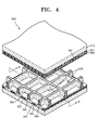
- FIG. 4 is an exploded perspective view of a PDP 300 according to another embodiment of the present invention
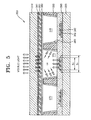
- FIG. 5 is a cross-sectional view of the PDP 300 of FIG. 4 taken along a line V-V'
- FIG. 6 is a cross-sectional view of quantum dots included in the PDP 300 of FIG 4.
- the PDP 300 includes a first substrate 310, a second substrate 320, barrier ribs 330, a first discharge electrode 341, a second discharge electrode 342, a first EL light-emitting layer 351, a second EL light-emitting layer 352, a phosphor layer 360, a dielectric layer 390, and a discharge gas.
- the first substrate 310 and the second substrate 320 are separated from each other and face each other.
- the first substrate 310 is formed of a transparent glass to transmit visible light.
- At least one barrier rib 330 is formed between the first substrate 310 and the second substrate 320.
- the barrier ribs 330 define the discharge cells 370 together with the first substrate 310 and the second substrate 320.
- the first discharge electrode 341 is formed on a rear surface of the first substrate 310 in a stripe pattern and is a transparent electrode formed of ITO.
- the first EL light-emitting layer 351 is formed on the first substrate 310 to cover and bury the first discharge electrode 341.
- the first EL light-emitting layer 351 is formed of quantum dots.
- the quantum dots have a quantum efficiency of up to 100 % and can be excited at a low voltage to increase the quantum efficiency.
- the quantum dots can be formed using a printing method that can be applied to large displays.
- the quantum dots are formed of a core 351a of CdSe, a shell 351b of ZnS surrounding the core 351a, and caps 351c of trioctylphosphine oxide (TOPO) disposed on an outer surface of the shell 351b.
- TOPO trioctylphosphine oxide
- the first EL light-emitting layer 351 can be formed as a single layer or a multi-layer structure. Generally, luminous efficiency is better when the first EL light-emitting layer 351 is a single layer.
- a protective layer 380 is formed on a rear surface of the first EL light-emitting layer 351.
- the protective layer 380 is formed of MgO.
- the protective layer 380 prevents the first discharge electrode 341 and the first EL light emitting layer 351 from being damaged by sputtering of plasma particles and reduces the discharge voltage by emitting second electrons.
- the second discharge electrode 342 is arranged to cross the first discharge electrode 341 and is formed in stripes on an upper surface of the second substrate 320.
- the second discharge electrode 342 is a transparent electrode formed of ITO like the first discharge electrode 341.
- the second EL light-emitting layer 352 is formed of the quantum dots used for the first EL light-emitting layer 351 and is disposed to cover a portion of the second discharge electrode 342. That is, the second EL light-emitting layer 352 does not bury the entire second discharge electrode 342. Thus, a width S2 of the second EL light-emitting layer 352 is less than a width S1 of the second discharge electrode 342.
- the dielectric layer 390 is additionally disposed to bury the second discharge electrode 342.
- the dielectric 390 can be formed of PbO, B 2 O 3 , or SiO 2 and covers not only the second discharge electrode 342 but also the second EL light-emitting layer 352.
- the dielectric layer 390 covers both the second discharge electrode 342 and the second EL light emitting layer 352.
- the present invention is not limited thereto. That is, the purpose of forming a dielectric layer is to protect a second discharge electrode from being exposed to the discharge space of the discharge cells. Thus, if the second discharge electrode has a structure that is not exposed to the discharge space due to the forming of a dielectric layer, the second EL light emitting layer does not necessarily have to be covered by the dielectric layer.
- the first discharge electrode 341 and the first EL light-emitting layer 351 are arranged close to each other and no layer is interposed therebetween.
- the second discharge electrode 342 and the second EL light-emitting layer 352 are arranged close to each other and no layer is interposed therebetween.
- the present invention is not limited thereto. That is, an additional dielectric layer can be further disposed between the first discharge electrode and the first EL light emitting layer or between the second discharge electrode and the second EL light emitting layer as occasions demand.
- barrier ribs 330 are formed on the dielectric layer 390 and the phosphor layer 360 is formed in the discharge cells 370 formed by the barrier ribs 330.
- the phosphor layer 360 is formed on sides of the barrier ribs 330 to prevent degradation of the phosphor layer 360 due to the plasma discharge.
- the phosphor layer 360 has a photoluminescent phosphor material element generating visible light by receiving ultraviolet rays. Red, green, and blue phosphor layers are formed according to the colours of visible light.
- the phosphor layer 360 includes the same phosphor materials as the phosphor layer 170 of FIG. 1 and thus a description thereof has not been repeated.
- the phosphor layer 360 is formed in the discharge cells 180; however, the present invention is not limited thereto. That is, the PDP of the present invention can omit a phosphor layer in the discharge cells and in this case only the EL light emitting layer emits light and the plasma discharge causes the light emitting of the EL light-emitting layer.
- the first discharge electrode 341, the second discharge electrode 342, the EL light emitting layer 351, the second EL light emitting layer 352, and the phosphor layer 360 are formed between the first substrate 310 and the second substrate 320, the first substrate 310 and the second substrate 320 are sealed using a material, such as frit.
- the air in the assembled PDP 300 is completely discharged and replaced with a suitable discharge gas that can improve the discharge efficiency.
- the discharge gas can be a mixed gas, such as Ne-Xe or He-Ne-Xe including Xe.
- the discharge gas can also include N 2 , D 2 , CO 2 , H 2 , CO, Ne, He, Ar, air at atmospheric pressure, and Kr.
- the radiated ultraviolet rays excite the phosphor materials of the phosphor layer 360 disposed in the discharge cells 370 and the energy level of the excited phosphor materials is decreased and red, green, and blue visible light is emitted.
- the first EL light-emitting layer 351 and the second EL light-emitting layer 352 are disposed on the plasma discharge path and current flows through the first EL light-emitting layer 351 and the second light-emitting layer 352 during the discharge. This is because the discharge voltage supplied to the first discharge electrode 341 and the second discharge electrode 342 is an AC voltage, and the voltage is supplied to each end of the first EL light-emitting layer 351 and the second EL light-emitting layer 352 functioning as dielectrics and a current flows therethrough. When a current flows through the first EL light-emitting layer 351 and the second EL light-emitting layer 352, visible light is emitted by an electron transition or a tunnel effect.
- the visible light emitted from the phosphor layer 360, the first EL light-emitting layer 351 and the second EL light-emitting layer 352 is combined and radiated through the first substrate 310 to the outside and thus the PDP 300 realizes an image.
- the PDP 300 since the PDP 300 includes the first and second EL light-emitting layers 351 and 352 including quantum dots, the visible light emitted from the quantum dots and the visible light emitted from the phosphor layer 360 are combined and emitted. Accordingly, the brightness of the PDP 300 according to the current embodiment of the present invention is better than that of a conventional PDP.
- the PDP 300 requires no additional power for driving the first and second EL light-emitting layers 351 and 352 and just the existing discharge voltage needs to be supplied to the first discharge electrode 341 and the second discharge electrode 342. Thus, the power consumed does not increase and the luminous efficiency is high.
- the PDP according to the present invention includes an EL light-emitting layer that emits light with the phosphor layer at the same time, thereby increasing the brightness of the PDP. Also, in a fine pitch panel, an improved brightness can be realized.
- the EL light-emitting layer operates only when a plasma discharge occurs in the discharging space of the discharge cells, improper emission does not occur.
- the PDP can omit a phosphor layer as occasion demands and in this case the structure is simple, thereby reducing the manufacturing costs. Also, the height of the barrier ribs can be reduced significantly, thus realizing very thin displays.
Abstract
Description
- The present invention relates to a Plasma Display Panel (PDP), and more particularly, the present invention relates to an opposed discharge PDP including an electroluminescent (EL) emitting layer.
- Recently, Plasma Display Panels (PDPs) have begun to be used as replacements for conventional Cathode Ray Tube (CRT) displays. In PDPs, a discharge gas is sealed inside two substrates on which a plurality of electrodes have been formed, and a discharge voltage is supplied to the electrodes to generate a plasma discharge to form a desired image.
- Generally, the brightness and efficiency of a PDP are the main factors that are considered when evaluating the capability of a PDP. One way to increase the brightness and efficiency is to increase a surface area of a phosphor layer. However, the brightness and efficiency of the PDP can only be increased by a limited amount by increasing the surface area of the PDP.
- Another way to increase the brightness of the PDP is to increase a discharge voltage supplied to the discharge electrodes. However, when the discharge voltage has reached a specific value, the brightness does not increase or the increase ratio of the brightness decreases, and accordingly, the efficiency of the PDP is reduced.
- Recently, since more fine pitch PDPs are being manufactured, the size of the discharge cells becomes small and the surface area of the phosphor layer coated in the discharge cells becomes small as well. Thus, the amount of visible light generated by each discharge cell decreases, thereby reducing the efficiency of the PDP.
- Accordingly, a new structure to increase the brightness and efficiency of PDPs is required.
- The present invention provides a Plasma Display Panel (PDP) having a structure that increases the brightness and efficiency of the PDP.
- According to one aspect of the present invention, a Plasma Display Panel (PDP) is provided including: a first substrate; a second substrate arranged to face the first substrate; barrier ribs arranged between the first and second substrates, the barrier ribs defining a plurality of discharge cells together with the first and second substrates; at least one first discharge electrode arranged on the first substrate; a first dielectric layer arranged on the first substrate to cover the at least one first discharge electrode; at least one second discharge electrode arranged on the second substrate; an Electroluminescent (EL) light-emitting layer arranged on at least a portion of the at least one second discharge electrode; and a discharge gas contained within the plurality of discharge cells.
- The EL light-emitting layer preferably includes a material selected from a group consisting of an inorganic EL light-emitting material and quantum dots. The EL light-emitting layer preferably has a thickness in a range of 500 to 5000 Å (50nm to 500nm), upon the EL light-emitting layer being the inorganic light-emitting material. The EL light-emitting layer preferably emits light in response to a discharge voltage being supplied to the at least one first discharge electrode and the at least one second discharge electrode.
- The inorganic EL light-emitting material preferably includes a material selected from a group consisting of ZnS:Mn, ZnS:Tb, SrS:Ce, Ca2S4:Ce, SrS:Cu,Ag, CaS:Pb and BaAl2S4:Eu.
- Each of the quantum dots preferably includes a core of CdSe, a cell of ZnS arranged to surround the core, and caps of Trioctylphosphine Oxide (TOPO) arranged on an outer surface of the cell.
- The PDP preferably further includes a dielectric layer arranged to bury the at least one second discharge electrode upon the EL light-emitting layer not burying the entire at least one second discharge electrode, the at least one second discharge electrode being exposed to a discharge space of the plurality of discharge cells. The PDP preferably further includes a dielectric layer arranged between the at least one second discharge electrode and the EL light-emitting layer.
- The PDP preferably further includes a phosphor layer arranged within the plurality of discharge cells. The phosphor layer preferably includes a material selected from a group consisting of a photoluminescent phosphor material and quantum dots.
- The PDP preferably further includes a protective layer arranged within the plurality of discharge cells.
- According to another aspect of the present invention, a Plasma Display Panel (PDP) is provided including: a first substrate; a second substrate arranged to face the first substrate; barrier ribs arranged between the first and second substrates to define a plurality of discharge cells together with the first and second substrates; at least one first discharge electrode arranged on the first substrate; a first Electroluminescent (EL) light-emitting layer arranged at least on a portion of the at least one first discharge electrode; at least one second discharge electrode arranged on the second substrate; a second EL light-emitting layer arranged at least on a portion of the at least one second discharge electrode; a discharge gas contained within the plurality of discharge cells.
- The first EL light emitting layer preferably includes a material selected from a group consisting of an inorganic EL light-emitting material and quantum dots. The first EL light-emitting layer preferably has a thickness in a range of 500 to 5000 Å (50 to 500nm) upon the first EL light-emitting layer being the inorganic light emitting material. The first EL light-emitting layer and the second EL light-emitting layer preferably emit light in response to a discharge voltage supplied to the at least one first discharge electrode and at least one the second discharge electrode.
- The inorganic EL light-emitting material is preferably a material selected from a group consisting of ZnS:Mn, ZnS:Tb, SrS:Ce, Ca2S4:Ce, SrS:Cu,Ag, CaS:Pb and BaAl2S4:Eu.
- Each of the quantum dots preferably includes a core CdSe, a cell of ZnS arranged to surround the core, and caps of Trioctylphosphine Oxide (TOPO) arranged on an outer surface of the cell.
- The second EL light-emitting layer preferably includes a material selected a group consisting of an inorganic light EL light emitting material and quantum dots. The second EL light-emitting layer preferably has a thickness in a range of 500 to 5000 Å (50 to 500nm) upon the second EL light-emitting layer being the inorganic light emitting material.
- The first EL light-emitting layer and the second EL light-emitting layer preferably emit light in response to a discharge voltage supplied to the at least one first discharge electrode and the at least one second discharge electrode.
- The inorganic EL light-emitting material is preferably a material selected from a group consisting of ZnS:Mn, ZnS:Tb, SrS:Ce, Ca2S4:Ce, SrS:Cu,Ag, CaS:Pb and BaAl2S4:Eu.
- Each of the quantum dots preferably include a core of CdSe, a cell of ZnS arranged to surround the core, and caps of Trioctylphosphine Oxide (TOPO) arranged on an outer surface of the cell.
- The PDP preferably further includes a dielectric layer arranged to bury the at least one first discharge electrode upon the first EL light-emitting layer not burying the entire at least one first discharge electrode, the at least one first discharge electrode being exposed to a discharge space of the plurality of discharge cells. The PDP preferably further includes a dielectric layer arranged to bury the at least one second discharge electrode upon the second EL light-emitting layer not burying the entire at least one second discharge electrode, the at least one second discharge electrode being exposed to a discharge space of the plurality of discharge cells. The PDP preferably further includes a dielectric layer arranged between the at least one first discharge electrode and the first EL light-emitting layer. The PDP preferably further includes a dielectric layer arranged between the at least one second discharge electrode and the second EL light-emitting layer.
- The PDP preferably further includes a phosphor layer arranged within the plurality of discharge cells. The phosphor layer preferably includes a material selected from a group consisting of a photoluminescent phosphor material and quantum dots.
- The PDP preferably further includes a protective layer arranged within the discharge cells.
- A more complete appreciation of the present invention and many of the attendant advantages thereof, will be readily apparent as the present invention becomes better understood by reference to the following detailed description when considered in conjunction with the accompanying drawings in which like reference symbols indicate the same or similar components, wherein:
- FIG. 1 is an exploded perspective view of a Plasma Display Panel (PDP) according to an embodiment of the present invention;
- FIG. 2 is a cross-sectional view of the PDP of FIG. 1 taken along a line II-II' according to an embodiment of the present invention;
- FIG. 3 is a cross-sectional view of a PDP according to another embodiment of the present invention;
- FIG. 4 is an exploded perspective view of a PDP according to another embodiment of the present invention;
- FIG. 5 is a cross-sectional view of the PDP of FIG. 4 taken along a line V-V'; and
- FIG. 6 is a cross-sectional view of quantum dots included in the PDP of FIG. 4.
- Referring to FIGS. 1 and 2, the
PDP 100 includes afirst substrate 110, asecond substrate 120,barrier ribs 130, afirst discharge electrode 141, asecond discharge electrode 142, a firstdielectric layer 151, an electroluminescent (EL)light emitting layer 160, aphosphor layer 170, and a discharge gas. - The
first substrate 110 and thesecond substrate 120 are separated from each other and are arranged to face each other. Thefirst substrate 110 is transparent to visible light. - Since the first substrate is transparent, visible light generated by a discharge is transmitted through the
first substrate 110. However, the present invention is not limited thereto. That is, the first substrate can be opaque and the second substrate transparent or both the first substrate and the second substrate can be transparent. Also, the first substrate and the second substrate can be semitransparent and a colour filter can be formed on a surface of the first and second substrates or inside the first and second substrates. - At least one
barrier rib 130 is formed between thefirst substrate 110 and thesecond substrate 120. Thebarrier ribs 130 are formed in a non-discharge area and definedischarge cells 180 together with thefirst substrate 110 and thesecond substrate 120 and prevent crosstalk of charged particles. - The
first discharge electrode 141 is formed of ITO. However, the present invention is not limited thereto. That is, the first discharge electrode can be formed of Ag, Cu, or Al, which are not transparent. However, if thefirst discharge electrode 141 is not transparent, thefirst discharge electrode 141 is divided into several narrow stripes to increase the transmittance of the visible light so that the light can be transmitted between the stripes. - The
first discharge electrode 141 of the present embodiment does not include a supplementary electrode to reduce line resistance. However, it is not limited thereto. That is, thefirst discharge electrode 141 can include a bus electrode formed of a material having a high electrical conductivity, such as Ag, to reduce line resistance. - The first
dielectric layer 151 is disposed on thefirst substrate 110 to cover and bury thefirst discharge electrode 141. Thefirst dielectric layer 151 prevents direct collision of the charged particles with thefirst discharge electrode 141 during dielectric discharge and accumulates wall discharge by inducing charged particles. The dielectric material can be PbO, B2O3, or SiO2. - A
protective layer 190 is formed on a rear surface of thefirst dielectric layer 151 and is formed of magnesium oxide (MgO). Theprotective layer 190 prevents thefirst discharge electrode 141 and thefirst dielectric layer 151 from being damaged by sputtering of plasma particles and generates secondary electrons to reduce the discharge voltage. Thesecond discharge electrode 142 is arranged in stripes to cross the extending direction of thefirst discharge electrode 141 and is formed of Ag, Cu, or Al. Thesecond discharge electrode 142 of the present embodiment is formed of Ag, Cu, or Al, which are not transparent. However, the material is not limited thereto. That is, thesecond discharge electrode 142 can be a transparent electrode formed of ITO. - The EL light-emitting
layer 160 is formed on thesecond substrate 120 to cover and bury thesecond discharge electrode 142. The EL light-emittinglayer 160 is formed of an inorganic EL light emitting material, such as ZnS:Mn, ZnS:Tb, SrS:Ce, Ca2S4:Ce, SrS:Cu,Ag, CaS:Pb, BaAl2S4:Eu. - Generally, when voltages of opposite polarities are supplied to opposite sides of an inorganic EL light emitting material, a current flows through the inorganic EL light-emitting material and an electron transition occurs in the inorganic EL light-emitting material to generate light. Since a discharge sustain voltage of the
PDP 100 is in the range of 150 V to 190 V, the inorganic EL light emitting materials used in the present embodiment can be inorganic EL light emitting materials which emit light in the range of the discharge sustain voltage of the PDP. Thus, ZnS:Mn type or ZnS:Tb type inorganic EL light emitting materials having a brightness of 4000 to 5000 cd/m2 can be used. - The thickness of the EL light-emitting
layer 160 can be in the range of 500 to 5000 Å (50 to 500nm). When the thickness of the EL light-emittinglayer 160 is greater than 5000 Å (500nm), the light transmittance is degraded and when the thickness of the ELlight emitting layer 160 is less than 500 Å (50nm), insufficient light is generated in the inorganic El light-emitting materials. - The EL
light emitting layer 160 of the present embodiment covers and buries thesecond discharge electrode 142. However, the present invention is not limited thereto. That is, the ELlight emitting layer 160 can cover and bury only a portion of thesecond discharge electrode 142. However, in this case, the second discharge electrode is exposed to a discharge space defined by thedischarge cells 180 and this direct exposure can cause thesecond discharge electrode 142 to be damaged by the discharge, and thus, a dielectric layer can be additionally formed to bury thesecond discharge electrode 142. - The EL
light emitting layer 160 of the present embodiment is formed of an inorganic EL light emitting material. However, the material is not limited thereto. That is, the EL light emitting layer can be formed of a material including quantum dots. - In the present embodiment, the
second discharge electrode 142 and the ELlight emitting layer 160 are formed very close to each other and no layer is interposed therebetween. However, the present invention is not limited thereto. That is, as occasion demands, a dielectric layer can be formed between thesecond discharge electrode 142 and the ELlight emitting layer 160. - The above described
barrier ribs 130 are formed on the ELlight emitting layer 160. Thebarrier ribs 130 can be formed using a sandblasting method or a printing method. Thebarrier ribs 130 can be also formed by forming sheets out of barrier ribs materials and boring holes in these sheets to define discharge cells. - As illustrated in FIG. 1, according to the current embodiment of the present invention, the cross-section of the
discharge cells 180 is a square. However, their shape is not limited thereto. That is, the cross-section of each of thedischarge cells 180 can be polygonal, such as a triangle, a pentagon, a circle or an oval and thebarrier ribs 130 can be formed in a stripe pattern such that each of thedischarge cells 180 are open. - A
phosphor layer 170 is formed in thedischarge cells 180 defined by thebarrier ribs 130. Thephosphor layer 170 is formed on a side surface of thebarrier ribs 130 and on a surface of the ELlight emitting layer 160. However, the present invention is not limited thereto. That is, if the PDP of the present invention includes a phosphor layer, the phosphor layer can be formed anywhere in the discharge cells of the PDP. - The
phosphor layer 170 has a photoluminescent phosphor material element generating visible light by receiving ultraviolet rays. Red, green, and blue phosphor layers according to the colours of visible light are formed. Red emitting phosphor layers formed in red discharge cells include a phosphor material, such as Y (V, P) O4:Eu, green emitting phosphor layers formed in green discharge cells include a phosphor material such, as Zn2SiO4:Mn, and blue emitting phosphor layers formed in blue discharge cells include a phosphor material, such as BaMgAl10O17:Eu. - The
phosphor layer 170 of the present embodiment is formed of a photoluminescent phosphor material. However, the present invention is not limited thereto. That is, thephosphor layer 170 can also be formed of a material including quantum dots. - In the present embodiment, the
phosphor layer 170 is formed in thedischarge cells 180; however, the present invention is not limited thereto. That is, the PDP of the present invention may not include a phosphor layer in the discharge cells and in this case, only the EL light emitting layer emits light and a plasma discharge contributes to light being emitted from the EL light-emitting layer. - As described above, after the
barrier ribs 130, thefirst discharge electrode 141, thesecond discharge electrode 142, thefirst dielectric layer 151, the ELlight emitting layer 160, and thephosphor layer 170 are formed between thefirst substrate 110 and thesecond substrate 120, thefirst substrate 110 and thesecond substrate 120 are sealed using a material such as a frit. - After the
first substrate 110 and thesecond substrate 120 are sealed, since the inner space of the assembledPDP 100 is filled with air, the air in the assembledPDP 100 is completely discharged and replaced with an adequate discharge gas that can improve the discharge efficiency. - The discharge gas can be a mixed gas, such as Ne-Xe or He-Ne-Xe including Xe. The discharge gas can also include N2, D2, CO2, H2, CO, Ne, He, Ar, air at atmospheric pressure, and Kr.
- Hereinafter is a description of an example of the discharge process of the
PDP 100 according to an embodiment of the present invention. - First, when a discharge voltage is supplied from an external power source to the
first discharge electrode 141 and thesecond discharge electrode 142 of thedischarge cells 180 in which discharge is to be generated, wall charges are accumulated between thefirst dielectric layer 151 and the EL light-emittinglayer 160. The accumulated wall charges move due to an AC discharge voltage and thus generate an opposed plasma discharge. Accordingly, the energy level of the discharge gas in thedischarge cells 180 is decreased and ultraviolet rays are radiated. - The radiated ultraviolet rays excite the phosphor materials of the
phosphor layer 170 and the energy level of the excited phosphor materials is decreased and red, green, and blue visible light is emitted. - The EL light-emitting
layer 160 is disposed on the plasma discharge path and current flows through the EL light-emittinglayer 160 during a discharge. This is because the discharge voltage supplied to thefirst discharge electrode 141 and thesecond discharge electrode 142 is an Alternating Current (AC) voltage, and the voltage is supplied to each end of the EL light-emittinglayer 160 functioning as a dielectric and current flows therethrough. When a current flows through the EL light-emittinglayer 160, visible light is emitted by an electron transition or a tunnel effect. - The visible light emitted from the
phosphor layer 170 and the EL light-emittinglayer 160 is combined and radiated through thefirst substrate 110 to the outside, and thus, thePDP 100 realizes an image. - The
PDP 100 according to the present embodiment includes an inorganic EL light-emitting material so that the visible light emitted from the inorganic EL light-emitting material and the visible light emitted from thephosphor layer 170 are combined and radiated, thus being brighter than conventional PDPs. - In addition, the
PDP 100 does not require additional power to drive the EL light-emittinglayer 160 and only the discharge voltage needs to be supplied to thefirst discharge electrode 141 and thesecond discharge electrode 142. Thus, the power consumed is not increased and the luminous efficiency is high. - Hereinafter, another example of the PDP of FIG. 1 is described with reference to FIG. 3. FIG. 3 is a cross-sectional view of a PDP 200according to another embodiment of the present invention. Descriptions of components common to the present embodiment and the previous embodiment have not been repeated.
- Referring to FIG. 3, the
PDP 200 includes afirst substrate 210, asecond substrate 220,barrier ribs 230, afirst discharge electrode 241, asecond discharge electrode 242, a firstdielectric layer 251, an EL light-emittinglayer 260 formed of an inorganic El light-emitting material, aprotective layer 290, and a discharge gas. - One of the main features distinguishing the
PDP 200 of FIG. 3 from thePDP 100 of FIG. 1 is that thePDP 200 does not include a phosphor layer. That is, since thePDP 200 does not include a phosphor layer, only the EL light-emittinglayer 260 emits visible light. - The plasma discharge functions mainly as a controlling switch of the light emitting from the EL light-emitting
layer 260 and the gap of the discharge gas area, that is, a distance d between theprotective layer 290 and the EL light-emittinglayer 260 can be 30 µm or less. This is because the smaller the distance d between theprotective layer 290 and the EL light-emittinglayer 260, the shorter the plasma discharge path, and thus, the current flowing through the EL light-emittinglayer 260 can be controlled promptly and the light emitting from the EL light-emittinglayer 260 can be easily controlled. - The characteristics of the
PDP 200 are as follows. - When a discharge voltage is supplied from an external power source to the
first discharge electrode 241 and thesecond discharge electrode 242 to generate a plasma discharge, a current flows through the EL light-emittinglayer 260 and visible light is emitted. When a plasma discharge is not generated, no current flows through the EL light-emittinglayer 260 and no visible light is emitted. - The plasma discharge supplies current to the EL light-emitting
layer 260 to control the EL light-emittinglayer 260 and the ultraviolet rays generated due to the plasma discharge are not converted into visible light. Accordingly, in the present embodiment, ultraviolet rays are not used and thePDP 200 can be driven using only Ne as a discharge gas. - The
PDP 200 does not require phosphor materials and has a simple structure, thereby reducing the manufacturing costs. Also, the height of thebarrier ribs 230 can be reduced significantly and a very thin display can be realized. - Also, since the
PDP 200 includes inorganic EL light-emitting materials as a light emitting source, thePDP 200 has the advantages of inorganic EL displays and also the memory characteristics and colour gradation realization driving method of conventional PDPs. - As the structure, operation, and effect of the
PDP 200 other than described herein are the same as the structure, operation, and effect of thePDP 100 of FIG. 1, descriptions thereof have not been repeated. - Hereinafter, a PDP according to another embodiment of the present invention is described with reference to FIGS. 4 through 6.
- FIG. 4 is an exploded perspective view of a
PDP 300 according to another embodiment of the present invention; FIG. 5 is a cross-sectional view of thePDP 300 of FIG. 4 taken along a line V-V'; and FIG. 6 is a cross-sectional view of quantum dots included in thePDP 300 of FIG 4. - Referring to FIGS. 4 and 5, the
PDP 300 includes afirst substrate 310, asecond substrate 320,barrier ribs 330, afirst discharge electrode 341, asecond discharge electrode 342, a first EL light-emittinglayer 351, a second EL light-emittinglayer 352, aphosphor layer 360, adielectric layer 390, and a discharge gas. - The
first substrate 310 and thesecond substrate 320 are separated from each other and face each other. Thefirst substrate 310 is formed of a transparent glass to transmit visible light. - At least one
barrier rib 330 is formed between thefirst substrate 310 and thesecond substrate 320. Thebarrier ribs 330 define thedischarge cells 370 together with thefirst substrate 310 and thesecond substrate 320. - The
first discharge electrode 341 is formed on a rear surface of thefirst substrate 310 in a stripe pattern and is a transparent electrode formed of ITO. The first EL light-emittinglayer 351 is formed on thefirst substrate 310 to cover and bury thefirst discharge electrode 341. The first EL light-emittinglayer 351 is formed of quantum dots. The quantum dots have a quantum efficiency of up to 100 % and can be excited at a low voltage to increase the quantum efficiency. The quantum dots can be formed using a printing method that can be applied to large displays. - The quantum dots are formed of a
core 351a of CdSe, ashell 351b of ZnS surrounding thecore 351a, and caps 351c of trioctylphosphine oxide (TOPO) disposed on an outer surface of theshell 351b. - The first EL light-emitting
layer 351 can be formed as a single layer or a multi-layer structure. Generally, luminous efficiency is better when the first EL light-emittinglayer 351 is a single layer. Aprotective layer 380 is formed on a rear surface of the first EL light-emittinglayer 351. Theprotective layer 380 is formed of MgO. - The
protective layer 380 prevents thefirst discharge electrode 341 and the first ELlight emitting layer 351 from being damaged by sputtering of plasma particles and reduces the discharge voltage by emitting second electrons. Thesecond discharge electrode 342 is arranged to cross thefirst discharge electrode 341 and is formed in stripes on an upper surface of thesecond substrate 320. - The
second discharge electrode 342 is a transparent electrode formed of ITO like thefirst discharge electrode 341. - The second EL light-emitting
layer 352 is formed of the quantum dots used for the first EL light-emittinglayer 351 and is disposed to cover a portion of thesecond discharge electrode 342. That is, the second EL light-emittinglayer 352 does not bury the entiresecond discharge electrode 342. Thus, a width S2 of the second EL light-emittinglayer 352 is less than a width S1 of thesecond discharge electrode 342. - Accordingly, as the
second discharge electrode 342 can be damaged by being exposed to the discharge space of thedischarge cells 370, thedielectric layer 390 is additionally disposed to bury thesecond discharge electrode 342. - The dielectric 390 can be formed of PbO, B2O3, or SiO2 and covers not only the
second discharge electrode 342 but also the second EL light-emittinglayer 352. - In the present embodiment, the
dielectric layer 390 covers both thesecond discharge electrode 342 and the second ELlight emitting layer 352. However, the present invention is not limited thereto. That is, the purpose of forming a dielectric layer is to protect a second discharge electrode from being exposed to the discharge space of the discharge cells. Thus, if the second discharge electrode has a structure that is not exposed to the discharge space due to the forming of a dielectric layer, the second EL light emitting layer does not necessarily have to be covered by the dielectric layer. - In the present embodiment, the
first discharge electrode 341 and the first EL light-emittinglayer 351 are arranged close to each other and no layer is interposed therebetween. Also in the present embodiment, thesecond discharge electrode 342 and the second EL light-emittinglayer 352 are arranged close to each other and no layer is interposed therebetween. However, the present invention is not limited thereto. That is, an additional dielectric layer can be further disposed between the first discharge electrode and the first EL light emitting layer or between the second discharge electrode and the second EL light emitting layer as occasions demand. - The above described
barrier ribs 330 are formed on thedielectric layer 390 and thephosphor layer 360 is formed in thedischarge cells 370 formed by thebarrier ribs 330. - The
phosphor layer 360 is formed on sides of thebarrier ribs 330 to prevent degradation of thephosphor layer 360 due to the plasma discharge. - The
phosphor layer 360 has a photoluminescent phosphor material element generating visible light by receiving ultraviolet rays. Red, green, and blue phosphor layers are formed according to the colours of visible light. - The
phosphor layer 360 includes the same phosphor materials as thephosphor layer 170 of FIG. 1 and thus a description thereof has not been repeated. - In the present embodiment, the
phosphor layer 360 is formed in thedischarge cells 180; however, the present invention is not limited thereto. That is, the PDP of the present invention can omit a phosphor layer in the discharge cells and in this case only the EL light emitting layer emits light and the plasma discharge causes the light emitting of the EL light-emitting layer. - As described above, after the
barrier ribs 330, thefirst discharge electrode 341, thesecond discharge electrode 342, the ELlight emitting layer 351, the second ELlight emitting layer 352, and thephosphor layer 360 are formed between thefirst substrate 310 and thesecond substrate 320, thefirst substrate 310 and thesecond substrate 320 are sealed using a material, such as frit. - After the
first substrate 310 and thesecond substrate 320 are sealed, since the inner space of the assembledPDP 300 is filled with air, the air in the assembledPDP 300 is completely discharged and replaced with a suitable discharge gas that can improve the discharge efficiency. - The discharge gas can be a mixed gas, such as Ne-Xe or He-Ne-Xe including Xe. The discharge gas can also include N2, D2, CO2, H2, CO, Ne, He, Ar, air at atmospheric pressure, and Kr.
- Hereinafter, an example of the discharge process of the
PDP 300 according to an embodiment of the present invention is described. - First, when a discharge voltage is supplied from an external power source to the
first discharge electrode 341 and thesecond discharge electrode 342 of thedischarge cells 180 in which discharge is to be generated, wall charges are accumulated between the EL light-emittinglayer 351 and thedielectric layer 390 which are facing each other. The accumulated wall charges move due to an AC discharge voltage and generate a plasma discharge. Accordingly, the energy level of the discharge gas is decreased and ultraviolet rays are radiated. - The radiated ultraviolet rays excite the phosphor materials of the
phosphor layer 360 disposed in thedischarge cells 370 and the energy level of the excited phosphor materials is decreased and red, green, and blue visible light is emitted. - The first EL light-emitting
layer 351 and the second EL light-emittinglayer 352 are disposed on the plasma discharge path and current flows through the first EL light-emittinglayer 351 and the second light-emittinglayer 352 during the discharge. This is because the discharge voltage supplied to thefirst discharge electrode 341 and thesecond discharge electrode 342 is an AC voltage, and the voltage is supplied to each end of the first EL light-emittinglayer 351 and the second EL light-emittinglayer 352 functioning as dielectrics and a current flows therethrough. When a current flows through the first EL light-emittinglayer 351 and the second EL light-emittinglayer 352, visible light is emitted by an electron transition or a tunnel effect. - The visible light emitted from the
phosphor layer 360, the first EL light-emittinglayer 351 and the second EL light-emittinglayer 352 is combined and radiated through thefirst substrate 310 to the outside and thus thePDP 300 realizes an image. - As described above, since the
PDP 300 includes the first and second EL light-emittinglayers phosphor layer 360 are combined and emitted. Accordingly, the brightness of thePDP 300 according to the current embodiment of the present invention is better than that of a conventional PDP. - Also, the
PDP 300 requires no additional power for driving the first and second EL light-emittinglayers first discharge electrode 341 and thesecond discharge electrode 342. Thus, the power consumed does not increase and the luminous efficiency is high. - As described above, the PDP according to the present invention includes an EL light-emitting layer that emits light with the phosphor layer at the same time, thereby increasing the brightness of the PDP. Also, in a fine pitch panel, an improved brightness can be realized.
- Also, no additional power to drive the EL light-emitting layer is required and just the existing discharge voltage during the sustain discharge needs to be supplied to the first discharge electrode and the second discharge electrode. Thus, no additional power is needed and the light efficiency of the PDP is improved.
- Also, since the EL light-emitting layer operates only when a plasma discharge occurs in the discharging space of the discharge cells, improper emission does not occur.
- Also, the PDP can omit a phosphor layer as occasion demands and in this case the structure is simple, thereby reducing the manufacturing costs. Also, the height of the barrier ribs can be reduced significantly, thus realizing very thin displays.
- While the present invention has been particularly shown and described with reference to exemplary embodiments thereof, it will be understood by those of ordinary skill in the art that various modifications in form and detail can be made therein without departing from the scope of the present invention as defined by the following claims.
Claims (15)
- A plasma display panel (PDP), comprising:first and second substrates;barrier ribs arranged between the first and second substrates, the barrier ribs defining a plurality of discharge cells;a first discharge electrode arranged on the first substrate;a second discharge electrode arranged on the second substrate;an electroluminescent (EL) light-emitting layer arranged on at least a portion of at least one of the first and second discharge electrodes; anda discharge gas contained within the plurality of discharge cells.
- The PDP of claim 1, further comprising a first dielectric layer arranged on the first substrate to cover the at least one first discharge electrode.
- The PDP of claim 1 or 2, wherein the EL light-emitting layer comprises an inorganic EL light-emitting material.
- The PDP of claim 3, wherein the EL light-emitting layer has a thickness in a range of 50 to 500nm.
- The PDP of claim 3 or 4, wherein the inorganic EL light-emitting material comprises a material selected from a group consisting of ZnS:Mn, ZnS:Tb, SrS:Ce, Ca2S4:Ce, SrS:Cu,Ag, CaS:Pb and BaAl2S4:Eu.
- The PDP of claim 1 or 2, wherein the EL light-emitting layer comprises quantum dots.
- The PDP of claim 6, wherein each of the quantum dots comprises a core of CdSe, a shell of ZnS arranged to surround the core, and caps of Trioctylphosphine Oxide (TOPO) arranged on an outer surface of the shell.
- The PDP of any one of the preceding claims, wherein the EL light-emitting layer emits light in response to a discharge voltage being supplied to the at least one first discharge electrode and the at least one second discharge electrode.
- The PDP of any one of the preceding claims, further comprising a dielectric layer arranged to cover the at least one second discharge electrode.
- The PDP of any one of the preceding claims, further comprising a dielectric layer arranged between a discharge electrode and a corresponding EL light-emitting layer disposed on the discharge electrode.
- The PDP of any one of the preceding claims, further comprising a phosphor layer arranged within the plurality of discharge cells.
- The PDP of claim 11, wherein the phosphor layer comprises a material selected from a group consisting of a photoluminescent phosphor material and quantum dots.
- The PDP of any one of the preceding claims, further comprising a protective layer arranged within the plurality of discharge cells.
- The PDP of any one of the preceding claims, wherein the EL light-emitting layer comprises an EL light-emitting layer disposed on at least a portion of the second discharge electrode.
- The PDP of any one of claims 1 to 13, wherein the EL light-emitting layer comprises a first EL light-emitting layer disposed on a portion of the first discharge electrode and a second EL light-emitting layer disposed on a portion of the second discharge electrode.
Applications Claiming Priority (1)
| Application Number | Priority Date | Filing Date | Title |
|---|---|---|---|
| KR1020050111984A KR100730170B1 (en) | 2005-11-22 | 2005-11-22 | Plasma display panel |
Publications (3)
| Publication Number | Publication Date |
|---|---|
| EP1788606A2 true EP1788606A2 (en) | 2007-05-23 |
| EP1788606A3 EP1788606A3 (en) | 2008-05-07 |
| EP1788606B1 EP1788606B1 (en) | 2009-06-03 |
Family
ID=37872307
Family Applications (1)
| Application Number | Title | Priority Date | Filing Date |
|---|---|---|---|
| EP06124514A Expired - Fee Related EP1788606B1 (en) | 2005-11-22 | 2006-11-21 | Plasma Display Panel |
Country Status (5)
| Country | Link |
|---|---|
| US (1) | US20070114929A1 (en) |
| EP (1) | EP1788606B1 (en) |
| JP (1) | JP2007141833A (en) |
| KR (1) | KR100730170B1 (en) |
| DE (1) | DE602006007081D1 (en) |
Families Citing this family (4)
| Publication number | Priority date | Publication date | Assignee | Title |
|---|---|---|---|---|
| US7372202B2 (en) * | 2004-04-22 | 2008-05-13 | The Board Of Trustees Of The University Of Illinois | Phase locked microdischarge array and AC, RF or pulse excited microdischarge |
| US8497631B2 (en) | 2006-01-23 | 2013-07-30 | The Board Of Trustees Of The University Of Illinois | Polymer microcavity and microchannel devices and fabrication method |
| WO2009055786A1 (en) * | 2007-10-25 | 2009-04-30 | The Board Of Trustees Of The University Of Illinois | Electron injection-controlled microcavity plasma device and arrays |
| KR102501705B1 (en) * | 2017-03-24 | 2023-02-21 | 삼성디스플레이 주식회사 | Transparent display panel and display device including the same |
Citations (3)
| Publication number | Priority date | Publication date | Assignee | Title |
|---|---|---|---|---|
| US4429303A (en) | 1980-12-22 | 1984-01-31 | International Business Machines Corporation | Color plasma display device |
| US20020063525A1 (en) | 2000-11-29 | 2002-05-30 | Choi Do-Hyun | Plasma switched organic electroluminescent display |
| EP1783804A2 (en) | 2005-11-08 | 2007-05-09 | Samsung SDI Co., Ltd. | Plasma display panel |
Family Cites Families (23)
| Publication number | Priority date | Publication date | Assignee | Title |
|---|---|---|---|---|
| US3686686A (en) * | 1969-12-08 | 1972-08-22 | Maclin S Hall | Visual display and memory system |
| JPH0632298B2 (en) * | 1987-08-31 | 1994-04-27 | シャープ株式会社 | Thin film EL display |
| JP3259253B2 (en) * | 1990-11-28 | 2002-02-25 | 富士通株式会社 | Gray scale driving method and gray scale driving apparatus for flat display device |
| US6097357A (en) * | 1990-11-28 | 2000-08-01 | Fujitsu Limited | Full color surface discharge type plasma display device |
| EP1231590A3 (en) * | 1991-12-20 | 2003-08-06 | Fujitsu Limited | Circuit for driving display panel |
| EP0554172B1 (en) * | 1992-01-28 | 1998-04-29 | Fujitsu Limited | Color surface discharge type plasma display device |
| JP3298659B2 (en) * | 1992-03-27 | 2002-07-02 | グンゼ株式会社 | Surface light emitting device using thin film EL device |
| US5828356A (en) * | 1992-08-21 | 1998-10-27 | Photonics Systems Corporation | Plasma display gray scale drive system and method |
| US5461395A (en) * | 1993-03-08 | 1995-10-24 | Tektronix, Inc. | Plasma addressing structure having a pliant dielectric layer |
| JP3025598B2 (en) * | 1993-04-30 | 2000-03-27 | 富士通株式会社 | Display driving device and display driving method |
| JP2891280B2 (en) * | 1993-12-10 | 1999-05-17 | 富士通株式会社 | Driving device and driving method for flat display device |
| JP3163563B2 (en) * | 1995-08-25 | 2001-05-08 | 富士通株式会社 | Surface discharge type plasma display panel and manufacturing method thereof |
| US6322901B1 (en) * | 1997-11-13 | 2001-11-27 | Massachusetts Institute Of Technology | Highly luminescent color-selective nano-crystalline materials |
| JP3019832B2 (en) * | 1998-02-27 | 2000-03-13 | 日本電気株式会社 | Plasma display panel |
| JP3424587B2 (en) * | 1998-06-18 | 2003-07-07 | 富士通株式会社 | Driving method of plasma display panel |
| US6114038A (en) * | 1998-11-10 | 2000-09-05 | Biocrystal Ltd. | Functionalized nanocrystals and their use in detection systems |
| KR20000074559A (en) * | 1999-05-21 | 2000-12-15 | 구자홍 | Plasma Address Electroluminescence Display Apparatus and Driving Method thereof |
| KR100333414B1 (en) * | 1999-09-04 | 2002-04-24 | 구자홍 | Plasma Address Electroluminescence Display Apparatus and Driving Method thereof |
| US6873106B2 (en) * | 2000-06-01 | 2005-03-29 | Pioneer Corporation | Plasma display panel that inhibits false discharge |
| KR20020070622A (en) * | 2001-03-02 | 2002-09-10 | 엘지전자 주식회사 | Structure of plasma display and fabricating method thereof |
| KR20020083405A (en) * | 2001-04-26 | 2002-11-02 | 씨엘디 주식회사 | Plasma Switched Organic Photoluminescent Display and Method of Making the Same |
| US20060170331A1 (en) * | 2003-03-11 | 2006-08-03 | Dietrich Bertram | Electroluminescent device with quantum dots |
| KR20060108632A (en) * | 2003-10-27 | 2006-10-18 | 마쯔시다덴기산교 가부시키가이샤 | Light-emitting device |
-
2005
- 2005-11-22 KR KR1020050111984A patent/KR100730170B1/en not_active IP Right Cessation
-
2006
- 2006-10-24 JP JP2006288803A patent/JP2007141833A/en active Pending
- 2006-11-17 US US11/600,879 patent/US20070114929A1/en not_active Abandoned
- 2006-11-21 EP EP06124514A patent/EP1788606B1/en not_active Expired - Fee Related
- 2006-11-21 DE DE602006007081T patent/DE602006007081D1/en not_active Expired - Fee Related
Patent Citations (3)
| Publication number | Priority date | Publication date | Assignee | Title |
|---|---|---|---|---|
| US4429303A (en) | 1980-12-22 | 1984-01-31 | International Business Machines Corporation | Color plasma display device |
| US20020063525A1 (en) | 2000-11-29 | 2002-05-30 | Choi Do-Hyun | Plasma switched organic electroluminescent display |
| EP1783804A2 (en) | 2005-11-08 | 2007-05-09 | Samsung SDI Co., Ltd. | Plasma display panel |
Also Published As
| Publication number | Publication date |
|---|---|
| US20070114929A1 (en) | 2007-05-24 |
| KR20070054030A (en) | 2007-05-28 |
| EP1788606B1 (en) | 2009-06-03 |
| KR100730170B1 (en) | 2007-06-19 |
| DE602006007081D1 (en) | 2009-07-16 |
| EP1788606A3 (en) | 2008-05-07 |
| JP2007141833A (en) | 2007-06-07 |
Similar Documents
| Publication | Publication Date | Title |
|---|---|---|
| US7750568B2 (en) | Plasma display panel (PDP) having a reflection preventive layer | |
| US20050179382A1 (en) | Plasma display panel | |
| EP1788606B1 (en) | Plasma Display Panel | |
| EP1783804B1 (en) | Plasma display panel | |
| KR100927619B1 (en) | Plasma Display Panel with Reduced Reflective Luminance | |
| KR100369074B1 (en) | Plasma Display Panel with Lattice -Type Ribs | |
| JP4342533B2 (en) | Plasma display panel | |
| US7486023B2 (en) | Single layer discharge electrode configuration for a plasma display panel | |
| EP1768155A1 (en) | Plasma display panel (PDP) | |
| EP1840930B1 (en) | Plasma display panel | |
| US20060119267A1 (en) | Plasma display panel | |
| US20080258603A1 (en) | Color display device | |
| KR100838072B1 (en) | Plasma display panel | |
| KR100615334B1 (en) | Plasma display panel | |
| KR100670339B1 (en) | Plasma display panel | |
| KR100760765B1 (en) | Plasma Display Panel | |
| KR100768207B1 (en) | Plasma display panel | |
| KR100749618B1 (en) | Plasma Display Panel | |
| KR20070005337A (en) | Plasma display panel | |
| KR20100073503A (en) | Phosphor compositions for white discharge cell and plasma display panel using the same | |
| KR20050112793A (en) | Plasma display panel | |
| US20080048938A1 (en) | Plasma display panel | |
| KR20080006886A (en) | Plasma display panel | |
| KR20070053552A (en) | Plasma display panel | |
| KR20050109205A (en) | Plasma display panel |
Legal Events
| Date | Code | Title | Description |
|---|---|---|---|
| PUAI | Public reference made under article 153(3) epc to a published international application that has entered the european phase |
Free format text: ORIGINAL CODE: 0009012 |
|
| 17P | Request for examination filed |
Effective date: 20061121 |
|
| AK | Designated contracting states |
Kind code of ref document: A2 Designated state(s): AT BE BG CH CY CZ DE DK EE ES FI FR GB GR HU IE IS IT LI LT LU LV MC NL PL PT RO SE SI SK TR |
|
| AX | Request for extension of the european patent |
Extension state: AL BA HR MK YU |
|
| PUAL | Search report despatched |
Free format text: ORIGINAL CODE: 0009013 |
|
| AK | Designated contracting states |
Kind code of ref document: A3 Designated state(s): AT BE BG CH CY CZ DE DK EE ES FI FR GB GR HU IE IS IT LI LT LU LV MC NL PL PT RO SE SI SK TR |
|
| AX | Request for extension of the european patent |
Extension state: AL BA HR MK RS |
|
| GRAP | Despatch of communication of intention to grant a patent |
Free format text: ORIGINAL CODE: EPIDOSNIGR1 |
|
| AKX | Designation fees paid |
Designated state(s): DE FR GB |
|
| GRAS | Grant fee paid |
Free format text: ORIGINAL CODE: EPIDOSNIGR3 |
|
| GRAA | (expected) grant |
Free format text: ORIGINAL CODE: 0009210 |
|
| AK | Designated contracting states |
Kind code of ref document: B1 Designated state(s): DE FR GB |
|
| REG | Reference to a national code |
Ref country code: GB Ref legal event code: FG4D |
|
| REF | Corresponds to: |
Ref document number: 602006007081 Country of ref document: DE Date of ref document: 20090716 Kind code of ref document: P |
|
| PLBE | No opposition filed within time limit |
Free format text: ORIGINAL CODE: 0009261 |
|
| STAA | Information on the status of an ep patent application or granted ep patent |
Free format text: STATUS: NO OPPOSITION FILED WITHIN TIME LIMIT |
|
| 26N | No opposition filed |
Effective date: 20100304 |
|
| REG | Reference to a national code |
Ref country code: FR Ref legal event code: ST Effective date: 20100730 |
|
| PG25 | Lapsed in a contracting state [announced via postgrant information from national office to epo] |
Ref country code: FR Free format text: LAPSE BECAUSE OF NON-PAYMENT OF DUE FEES Effective date: 20091130 |
|
| PG25 | Lapsed in a contracting state [announced via postgrant information from national office to epo] |
Ref country code: DE Free format text: LAPSE BECAUSE OF NON-PAYMENT OF DUE FEES Effective date: 20100601 |
|
| GBPC | Gb: european patent ceased through non-payment of renewal fee |
Effective date: 20101121 |
|
| PG25 | Lapsed in a contracting state [announced via postgrant information from national office to epo] |
Ref country code: GB Free format text: LAPSE BECAUSE OF NON-PAYMENT OF DUE FEES Effective date: 20101121 |