EP1793451A1 - Compact broadband patch antenna - Google Patents
Compact broadband patch antenna Download PDFInfo
- Publication number
- EP1793451A1 EP1793451A1 EP06125075A EP06125075A EP1793451A1 EP 1793451 A1 EP1793451 A1 EP 1793451A1 EP 06125075 A EP06125075 A EP 06125075A EP 06125075 A EP06125075 A EP 06125075A EP 1793451 A1 EP1793451 A1 EP 1793451A1
- Authority
- EP
- European Patent Office
- Prior art keywords
- patch
- antenna
- driver
- ground plane
- substrate
- Prior art date
- Legal status (The legal status is an assumption and is not a legal conclusion. Google has not performed a legal analysis and makes no representation as to the accuracy of the status listed.)
- Withdrawn
Links
Images


Classifications
-
- H—ELECTRICITY
- H01—ELECTRIC ELEMENTS
- H01Q—ANTENNAS, i.e. RADIO AERIALS
- H01Q9/00—Electrically-short antennas having dimensions not more than twice the operating wavelength and consisting of conductive active radiating elements
- H01Q9/04—Resonant antennas
- H01Q9/0407—Substantially flat resonant element parallel to ground plane, e.g. patch antenna
- H01Q9/0442—Substantially flat resonant element parallel to ground plane, e.g. patch antenna with particular tuning means
Definitions
- the present invention relates to communications antennas, and more specifically relates to a novel microstrip patch antenna suitable for use in an antenna array.
- a modem trend in the design of antennas for wireless devices is to combine two or more antenna elements into an antenna array.
- Each antenna element in such an array should have a small footprint, a low level of mutual coupling with neighboring elements, a low element return loss, a low axial ratio (in case of circular polarization), and a large frequency bandwidth.
- these requirements are typically at odds with each other. For example, the larger the bandwidth and the larger the size of an antenna element, the stronger will be the mutual coupling between the antenna element and its neighboring elements in the antenna array.
- FIG. 1 depicts a conventional patch antenna element 100 for use in an antenna array.
- Patch antenna element 100 includes a driver patch 110 and a ground plane 130, separated by a dielectric substrate 120.
- An input signal having a given wavelength ⁇ is inserted via a microstrip feed line (not shown) connected to the driver patch 110.
- the length L of the patch is typically selected to be 1 ⁇ 2 of the wavelength, so that the patch resonates at the signal frequency of the signal and thereby transmits the desired wireless signal.
- the wavelength ⁇ can be very long, and the patch antenna dimension L can become quite large.
- the high permittivity substrate reduces the resonant frequency of the patch antenna element 100 and thus allows a smaller driver patch to be used for a given signal frequency f.
- the length of the driver patch is conventionally selected to be inversely proportional to the square root of the permittivity ⁇ S of the substrate 120.
- the length L were nominally 1 cm for a substrate permittivity of 1, the length L could be reduced to 0.5 cm for a substrate having a permittivity of 4 were used, or to 0.33 cm for a substrate having a permittivity of 9.
- the effect of the increased dielectric permittivity is to raise the capacitance between the patch 110 and ground plane 130 and thereby to lower the resonant frequency.
- the reduced antenna volume decreases the bandwidth of the antenna element and causes difficulties with impedance matching.
- the bandwidth may be improved to some extent by increasing the thickness of the substrate.
- a thicker substrate introduces additional problems by (i) increasing the antenna's cost; (ii) increasing the antenna's mass (or weight), which may be unacceptable in space applications; and (iii) exciting unwanted electromagnetic waves at the substrate's surface, which lead to poor radiation efficiency, larger mutual coupling between antenna elements and distorted radiation patterns.
- a very thin substrate is conventionally used for the feed network - including, e.g., the microstrip feed line (not shown) - and it is preferable to build antenna elements with the same substrate as that used for the feed network.
- FIG. 2 depicts another known technique to improve the bandwidth of an antenna element by adding a parasitic patch above the driver patch, resulting in a "stacked patch antenna.”
- Stacked patch antennas have been described in the article entitled “ Stacked Microstrip Antenna with Wide Bandwidth and High Gain” by Egashira et al., published in IEEE Transactions on Antennas and Propagation, Vol. 44, No. 11 (Nov. 1996 ); and in U.S. Patent Nos. 6,759,986 ; 6,756,942 ; and 6,806,831 . As shown in FIG.
- a conventional stacked patch antenna 200 includes a ground plane 250 supporting a dielectric substrate 240, a driver patch 230, a foam dielectric 220 having a permittivity similar to air, and a parasitic patch 210 (also known as a "driven patch” or "stacked patch”).
- a signal to be transmitted is input to the driver patch 230.
- the parasitic patch 210 is electromagnetically coupled to the driver patch 230 and therefore resonates with it.
- the additional resonance provided by the parasitic patch 210 improves the operational frequency of the stacked patch antenna 200 and increases the bandwidth of the antenna.
- parasitic patch 210 In conventional stacked patch antennas, however, parasitic patch 210 must be fairly large in comparison with driver patch 230, as reflected in FIG. 2, due to the relatively low permittivity of the foam dielectric 220.
- the performance of a patch antenna is compromised in order to reduce the size of the antenna. Accordingly, there is a need for a patch antenna that requires a smaller volume than existing antennas without compromising the performance of the antenna.
- the present invention fulfills this need among others.
- a patch antenna for transmitting or receiving a wireless signal comprising a base layer having a cavity; a ground plane located on the base layer, and having an opening over at least a portion of the cavity, a substrate located on the ground plane; and a driver patch located on the substrate.
- the solution is also provided by a corresponding method for constructing a compact broadband patch antenna, comprising the steps of: providing a base layer having a cavity, providing a ground plane located on the base layer, and having an opening over at least a portion of the cavity; providing a substrate located on the ground plane; and providing a driver patch located on the substrate.
- the present invention provides for a compact broadband patch antenna in which a cavity is etched in a substrate under the driver patch.
- the inventors have discovered that the cavity expands the electromagnetic volume of the antenna element and greatly enhances the efficiency and bandwidth of the antenna by reducing the capacitive loading of the driver patch. Indeed, the efficiency of the antenna may be increased from about 45 % (for very thin substrates) to 95 % (for thicker substrates).
- the inventors have found that the use of the cavity in this manner greatly increases the capacitive loading of the parasitic patch, which in turn significantly improves the resonant frequency characteristics of the patch antenna.
- the broadband patch antenna in accordance with the invention takes up a significantly smaller surface area on an integrated patch antenna die and has a much smaller mass than a conventional patch antenna having the same resonant frequency.
- the size, location and/or shape of the opening in the ground plane maybe adjusted during the design of the antenna in order to obtain a desired capacitive loading from the patch to the ground plane. Because the capacitive loading largely determines the resonant frequency of the driver patch, a desired resonant frequency of the driver patch can be set during the design of the antenna simply by selecting an appropriate geometry (size, shape and/or location) for the opening in the ground plane.
- the broadband patch antenna may include a parasitic patch, located over and separated from the driver patch by a radome or a layer of foam or other dielectric material.
- the driver patch and/or the parasitic patch may also include one or more slots, which further reduce the size of the antenna element and improve the performance of the antenna element and the associated antenna array.
- an embodiment of the broadband patch antenna 300 is shown in a cross-sectional view (FIG. 3A), a top view (FIG. 3B) and a bottom view (FIG. 3C).
- the illustrated device comprises a base layer 390 having a cavity 350, a ground plane 330 having an opening 340 (shown in FIG. 3C), a dielectric substrate 320, which is preferably thin, and a driver patch or microstrip patch 310.
- an input signal is preferably provided to the driver patch 310 via a microstrip line 395 (in FIG. 3B) and radiated outward by driver patch 310.
- the input signal may be provided via a coaxial probe feed passing upward through the base layer 390, cavity 350, and opening 340 to the driver patch 310.
- the opening of the ground plane 330 may be larger than, coextensive with, or smaller than the cavity or the driver patch 310.
- Ground plane 330 is preferably extended beneath driver patch 310, such that at least a portion of the ground plane 330 overlaps the driver patch 310.
- the ground plane opening 340 is centered over, and smaller than, the cavity 350, such that the ground plane 330 overlaps the driver patch 310 around the entire perimeter of the ground plane opening 340.
- the overlap between the ground plane and the driver patch is selected based upon the thickness of the substrate. For thinner substrates, for example, the overlap could be as small as 0.01 ⁇ (one-hundredth of a wavelength).
- This overlap helps to lower the resonant frequency of the broadband patch antenna 300 by capacitively loading the driver patch 310. It thereby also helps to reduce the overall size of broadband patch antenna 300 without loading the cavity with a dielectric. It should be noted, however, that the broadband patch antenna 300 is suitable for operation without this overlap.
- Base layer 390 is preferably a metal material, in the form of a block, such as aluminum, steel, silver or gold, milled or machined to form cavity 350.
- base layer 390 may be a semiconductive or insulating material formed by conventional photolithographic techniques. If base layer 390 is a semiconductor or insulator (e.g., a dielectric material), however, then the performance of the broadband patch antenna may be improved by lining the surfaces 360, 370, 380 of cavity 350 with a thin layer of conductive material, preferably a metal such as silver or gold.
- the metal lining on vertical surfaces 360 and 370 of the cavity may be provided in the form of an array of metal vias (not shown) around the perimeter of cavity 350, preferably at distances of approximately 1/8 to 1/10 of the wavelength. In this way, the electromagnetic field emitted by the driver patch 310 is contained and reflected back toward driver patch 310.
- the cavity 350 serves to improve the radiation efficiency and thereby also to lower the overall dissipation loss of the driver patch. Without the back cavity, the currents in the driver patch 310 tend to be non-uniform, causing a higher resistive loss and thus lower radiation efficiency. In contrast, in the presence of the back cavity, the radiation efficiency is improved, because the effective dielectric thickness (thin substrate plus air cavity) is larger. By way of example, for thin substrates, the cavity helps to improve the radiation efficiency from about 50% to 90%.
- the cavity 350 also serves to improve the bandwidth of the broadband patch antenna by increasing the effective volume of the antenna below the driver patch. In general, the larger the volume, the better will be the resulting antenna bandwidth (until saturation eventually occurs).
- the bandwidth of the antenna is greatly enhanced. For example, without the cavity, the bandwidth will typically be in the range of about two to five percent of the centre operating frequency.
- the bandwidth would be five percent of 10 GHz, or 0.5 GHz, such that the conventional patch antenna would operate from 9.75 GHz to 10.25 GHz.
- a bandwidth in the range from about 10 to 16% may be achieved.
- the cavity width is preferably slightly larger than that of the driver patch 310, and the cavity depth is preferably in the range of 0.01 to 0.02 times the signal wavelength. Because the cavity depth may be very small, it adds very little additional volume to the antenna array.
- Cavity 350 in base layer 390 may also be filled or unfilled. Filling the cavity 350 with foam or another suitable dielectric material advantageously provides structural support to driver patch 310.
- Substrate 320 may be any low loss substrate material conventionally used by those of skill in the art for constructing patch antennas, such as RT Duroid ® or a Teflon ® -based substrate as manufactured by Rogers Corporation, Taconic ® and Arlon, Inc. Such substrates typically have a permittivity of about 2 to about 6.
- Ground plane 330 and driver patch 310 may be any conductive material (including copper, aluminum, silver or gold).
- ground plane 330 is preferably formed by depositing the conductive material on the bottom surface of the dielectric substrate, while driver patch 310 is formed by depositing the conductive material on the top surface of the dielectric substrate.
- Suitable dimensions for the compact broadband patch antenna shown in FIGs. 3A-3C signals may be selected using electromagnetic simulation techniques of the type conventionally used by those of skill in the art in the design of patch antennas.
- Suitable 3D electromagnetic simulation software packages include CST Microwave Studio® by CST of America, Inc. and HFSS TM by Ansoft Corp.
- FIGs. 4 and 5 illustrate further embodiments of compact broadband patch antennae in accordance with the invention.
- antenna 400 in FIG. 4 further includes a parasitic patch 410, mounted under a radome 405.
- parasitic patch 410 resonates with the signal emitted by driver patch 310 and thereby improves the radiation characteristics of driver patch 310.
- Parasitic patch 410 may be supported by a radome 405 (as in FIG. 4) or by a dielectric material 505 (as in FIG. 5).
- Radome 405 in FIG. 4 is preferably a polycarbonate material that provides structural support to resonant patch 410 and physical protection to the broadband patch antenna 400.
- Dielectric material 505 in FIG. 5 is preferably foam or dielectric foam but may alternatively be formed from other dielectric materials. Because the permittivity of foam tends to be low (e.g., ⁇ FOAM ⁇ 1), however, parasitic patch 410 may need to have a larger area than driver patch 310, if foam is used to support resonant patch 410.
- FIG. 6 illustrates a further embodiment of a broadband patch antenna as in FIG. 3, to which slots 610 and 620 have been added in the parasitic patch 410, perpendicular to the direction of the electromagnetic field (shown by the thick arrow) in the parasitic patch 410.
- These slots 610 and 620 provide a longer current path for electrical currents in the parasitic patch 410, thereby artificially increasing the electrical length of the current paths. Accordingly, the dimensions of the stacked patch antenna 400 may be made smaller without negatively impacting the antenna characteristics. Alternatively, a single slot may also be used.
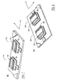
- FIGs. 7 and 8 illustrate the manner in which the slotted broadband patch antenna of FIG. 6 may be implemented in an antenna array.
- the slots are preferably positioned perpendicular to the direction of the electrical field E - i.e., perpendicular to the antenna's E-plane and parallel to its H-plane.
- E-plane of an antenna is defined as "for a linearly polarized antenna, the plane containing the electric field vector and the direction of maximum radiation," per IEEE Standard Definitions of Terms for Antennas, Std 145-1993.
- the "H-plane" lies orthogonal to the E-plane and may be defined as "for a linearly polarized antenna, the plane containing the magnetic field vector and the direction of maximum radiation.
- each broadband patch antenna should be aligned end-to-end, as shown, parallel to the direction of H-plane coupling.
- the slots 820, 830, 850 and 860 for each broadband patch antenna should be placed in parallel as shown, perpendicular to the E-plane coupling.
- the use of slots in the resonant patch element and their arrangement perpendicular to the E-field results as shown in FIGs. 6 through 8 greatly reduce the size of the patch and hence the mutual coupling between neighboring antenna elements, and thereby improve antenna gain response, radiation patterns, and scanning performance.
- the patch antenna in accordance with the present invention provides several advantages over existing patch antennas.
- a smaller antenna with better performance can be achieved.
- the patch antenna of the present invention does not require a high dielectric constant substrate to get a low resonant frequency, it has a very high efficiency and low mass.
Abstract
Description
- The present invention relates to communications antennas, and more specifically relates to a novel microstrip patch antenna suitable for use in an antenna array.
- A modem trend in the design of antennas for wireless devices is to combine two or more antenna elements into an antenna array. Each antenna element in such an array should have a small footprint, a low level of mutual coupling with neighboring elements, a low element return loss, a low axial ratio (in case of circular polarization), and a large frequency bandwidth. For a typical antenna element in an antenna array, however, these requirements are typically at odds with each other. For example, the larger the bandwidth and the larger the size of an antenna element, the stronger will be the mutual coupling between the antenna element and its neighboring elements in the antenna array.
- FIG. 1 depicts a conventional
patch antenna element 100 for use in an antenna array.Patch antenna element 100 includes adriver patch 110 and aground plane 130, separated by adielectric substrate 120. An input signal having a given wavelength λ is inserted via a microstrip feed line (not shown) connected to thedriver patch 110. The length L of the patch is typically selected to be ½ of the wavelength, so that the patch resonates at the signal frequency of the signal and thereby transmits the desired wireless signal. At low frequencies, however, the wavelength λ can be very long, and the patch antenna dimension L can become quite large. - A known technique to reduce the size of the patch antenna element is to select a
dielectric substrate 120 with a very high permittivity εS (e.g., εS = 6 to 20 relative to air). The high permittivity substrate reduces the resonant frequency of thepatch antenna element 100 and thus allows a smaller driver patch to be used for a given signal frequency f. More specifically, for the patch antenna element shown in FIG. 1, and for a given signal frequency f, the length of the driver patch is conventionally selected to be inversely proportional to the square root of the permittivity εS of thesubstrate 120. For example, if the length L were nominally 1 cm for a substrate permittivity of 1, the length L could be reduced to 0.5 cm for a substrate having a permittivity of 4 were used, or to 0.33 cm for a substrate having a permittivity of 9. - The effect of the increased dielectric permittivity is to raise the capacitance between the
patch 110 andground plane 130 and thereby to lower the resonant frequency. Unfortunately, the reduced antenna volume decreases the bandwidth of the antenna element and causes difficulties with impedance matching. Using conventional design methods known to those of skill in the art, the bandwidth may be improved to some extent by increasing the thickness of the substrate. A thicker substrate, however, introduces additional problems by (i) increasing the antenna's cost; (ii) increasing the antenna's mass (or weight), which may be unacceptable in space applications; and (iii) exciting unwanted electromagnetic waves at the substrate's surface, which lead to poor radiation efficiency, larger mutual coupling between antenna elements and distorted radiation patterns. Moreover, a very thin substrate is conventionally used for the feed network - including, e.g., the microstrip feed line (not shown) - and it is preferable to build antenna elements with the same substrate as that used for the feed network. - FIG. 2 depicts another known technique to improve the bandwidth of an antenna element by adding a parasitic patch above the driver patch, resulting in a "stacked patch antenna." Stacked patch antennas have been described in the article entitled "Stacked Microstrip Antenna with Wide Bandwidth and High Gain" by Egashira et al., published in IEEE Transactions on Antennas and Propagation, Vol. 44, No. 11 (Nov. 1996); and in
U.S. Patent Nos. 6,759,986 ;6,756,942 ; and6,806,831 . As shown in FIG. 2, a conventional stackedpatch antenna 200 includes aground plane 250 supporting adielectric substrate 240, adriver patch 230, a foam dielectric 220 having a permittivity similar to air, and a parasitic patch 210 (also known as a "driven patch" or "stacked patch"). A signal to be transmitted is input to thedriver patch 230. Theparasitic patch 210 is electromagnetically coupled to thedriver patch 230 and therefore resonates with it. The additional resonance provided by theparasitic patch 210 improves the operational frequency of the stackedpatch antenna 200 and increases the bandwidth of the antenna. In conventional stacked patch antennas, however,parasitic patch 210 must be fairly large in comparison withdriver patch 230, as reflected in FIG. 2, due to the relatively low permittivity of the foam dielectric 220. As a result, when stacked patch antenna elements are combined in an antenna array, adjacent elements exhibit a strong mutual coupling effect on each other, which negatively impacts on antenna element and array gain, radiation patterns, bandwidth and scanning ability of the antenna array. Furthermore, in view of recent trends in miniaturization, conventional stacked patch antennas are still too large. - Thus, in conventional designs, the performance of a patch antenna is compromised in order to reduce the size of the antenna. Accordingly, there is a need for a patch antenna that requires a smaller volume than existing antennas without compromising the performance of the antenna. The present invention fulfills this need among others.
- The solution is provided by a patch antenna for transmitting or receiving a wireless signal comprising a base layer having a cavity; a ground plane located on the base layer, and having an opening over at least a portion of the cavity, a substrate located on the ground plane; and a driver patch located on the substrate.
- The solution is also provided by a corresponding method for constructing a compact broadband patch antenna, comprising the steps of: providing a base layer having a cavity, providing a ground plane located on the base layer, and having an opening over at least a portion of the cavity; providing a substrate located on the ground plane; and providing a driver patch located on the substrate.
- The invention will now be described by way of example with reference to the accompanying drawings in which:
- Figure 1 is a cross-sectional view of a patch antenna in accordance with the prior art.
- Figure 2 is a cross-sectional view of a stacked patch antenna in accordance with the prior art
- Figure 3A is a cross-sectional side view of a broadband patch antenna in accordance with the present invention.
- Figure 3B is a top view of the substrate of the broadband patch antenna in accordance with the present invention.
- Figure 3C is a bottom view of the substrate of the broadband patch antenna in accordance with the present invention.
- Figure 4 is a cross-sectional view of a broadband patch antenna having a parasitic patch mounted on a radome in accordance with the present invention.
- Figure 5 is a cross-sectional view of a broadband patch antenna having a parasitic patch mounted on a foam layer in accordance with the present invention.
- Figure 6 is an isometric view of a broadband patch antenna having a parasitic patch with slots in accordance with the present invention.
- Figure 7 is an isometric view of an antenna array including two broadband patch antenna elements in accordance with the present invention, coupled in the H-Plane.
- Figure 8 is an isometric view of an antenna array including two broadband patch antenna elements in accordance with the present invention, coupled in the E-Plane.
- The present invention provides for a compact broadband patch antenna in which a cavity is etched in a substrate under the driver patch. The inventors have discovered that the cavity expands the electromagnetic volume of the antenna element and greatly enhances the efficiency and bandwidth of the antenna by reducing the capacitive loading of the driver patch. Indeed, the efficiency of the antenna may be increased from about 45 % (for very thin substrates) to 95 % (for thicker substrates).
- The inventors have found that the use of the cavity in this manner greatly increases the capacitive loading of the parasitic patch, which in turn significantly improves the resonant frequency characteristics of the patch antenna. As a result, for a given resonant frequency, the broadband patch antenna in accordance with the invention takes up a significantly smaller surface area on an integrated patch antenna die and has a much smaller mass than a conventional patch antenna having the same resonant frequency.
- Advantageously, the size, location and/or shape of the opening in the ground plane maybe adjusted during the design of the antenna in order to obtain a desired capacitive loading from the patch to the ground plane. Because the capacitive loading largely determines the resonant frequency of the driver patch, a desired resonant frequency of the driver patch can be set during the design of the antenna simply by selecting an appropriate geometry (size, shape and/or location) for the opening in the ground plane.
- In still further embodiments, the broadband patch antenna may include a parasitic patch, located over and separated from the driver patch by a radome or a layer of foam or other dielectric material. The driver patch and/or the parasitic patch may also include one or more slots, which further reduce the size of the antenna element and improve the performance of the antenna element and the associated antenna array.
- Referring to Figures 3A, 3B, and 3C, an embodiment of the
broadband patch antenna 300 is shown in a cross-sectional view (FIG. 3A), a top view (FIG. 3B) and a bottom view (FIG. 3C). The illustrated device comprises abase layer 390 having acavity 350, aground plane 330 having an opening 340 (shown in FIG. 3C), adielectric substrate 320, which is preferably thin, and a driver patch ormicrostrip patch 310. As inconventional patch antenna 100 described above, an input signal is preferably provided to thedriver patch 310 via a microstrip line 395 (in FIG. 3B) and radiated outward bydriver patch 310. Alternatively, the input signal may be provided via a coaxial probe feed passing upward through thebase layer 390,cavity 350, and opening 340 to thedriver patch 310. - The opening of the
ground plane 330 may be larger than, coextensive with, or smaller than the cavity or thedriver patch 310.Ground plane 330 is preferably extended beneathdriver patch 310, such that at least a portion of theground plane 330 overlaps thedriver patch 310. Still more preferably, theground plane opening 340 is centered over, and smaller than, thecavity 350, such that theground plane 330 overlaps thedriver patch 310 around the entire perimeter of the ground plane opening 340. Preferably, the overlap between the ground plane and the driver patch is selected based upon the thickness of the substrate. For thinner substrates, for example, the overlap could be as small as 0.01λ (one-hundredth of a wavelength). This overlap helps to lower the resonant frequency of thebroadband patch antenna 300 by capacitively loading thedriver patch 310. It thereby also helps to reduce the overall size ofbroadband patch antenna 300 without loading the cavity with a dielectric. It should be noted, however, that thebroadband patch antenna 300 is suitable for operation without this overlap. -
Base layer 390 is preferably a metal material, in the form of a block, such as aluminum, steel, silver or gold, milled or machined to formcavity 350. Alternatively,base layer 390 may be a semiconductive or insulating material formed by conventional photolithographic techniques. Ifbase layer 390 is a semiconductor or insulator (e.g., a dielectric material), however, then the performance of the broadband patch antenna may be improved by lining thesurfaces cavity 350 with a thin layer of conductive material, preferably a metal such as silver or gold. The metal lining onvertical surfaces cavity 350, preferably at distances of approximately 1/8 to 1/10 of the wavelength. In this way, the electromagnetic field emitted by thedriver patch 310 is contained and reflected back towarddriver patch 310. - As described above, the
cavity 350 serves to improve the radiation efficiency and thereby also to lower the overall dissipation loss of the driver patch. Without the back cavity, the currents in thedriver patch 310 tend to be non-uniform, causing a higher resistive loss and thus lower radiation efficiency. In contrast, in the presence of the back cavity, the radiation efficiency is improved, because the effective dielectric thickness (thin substrate plus air cavity) is larger. By way of example, for thin substrates, the cavity helps to improve the radiation efficiency from about 50% to 90%. - Further, because the bandwidth of a stacked patch antenna is typically proportional to its volume (i.e., the volume below the driver patch), the
cavity 350 also serves to improve the bandwidth of the broadband patch antenna by increasing the effective volume of the antenna below the driver patch. In general, the larger the volume, the better will be the resulting antenna bandwidth (until saturation eventually occurs). By expanding the three-dimensional volume of the antenna below the ground plane and into the space formed by thecavity 350, the bandwidth of the antenna is greatly enhanced. For example, without the cavity, the bandwidth will typically be in the range of about two to five percent of the centre operating frequency. In other words, if the centre frequency is 10 GHz, the bandwidth would be five percent of 10 GHz, or 0.5 GHz, such that the conventional patch antenna would operate from 9.75 GHz to 10.25 GHz. In contrast, with the cavity, a bandwidth in the range from about 10 to 16% may be achieved. - Dimensionally speaking, the cavity width is preferably slightly larger than that of the
driver patch 310, and the cavity depth is preferably in the range of 0.01 to 0.02 times the signal wavelength. Because the cavity depth may be very small, it adds very little additional volume to the antenna array. -
Cavity 350 inbase layer 390 may also be filled or unfilled. Filling thecavity 350 with foam or another suitable dielectric material advantageously provides structural support todriver patch 310. -
Substrate 320 may be any low loss substrate material conventionally used by those of skill in the art for constructing patch antennas, such as RT Duroid® or a Teflon®-based substrate as manufactured by Rogers Corporation, Taconic® and Arlon, Inc. Such substrates typically have a permittivity of about 2 to about 6. -
Ground plane 330 anddriver patch 310 may be any conductive material (including copper, aluminum, silver or gold). In practice,ground plane 330 is preferably formed by depositing the conductive material on the bottom surface of the dielectric substrate, whiledriver patch 310 is formed by depositing the conductive material on the top surface of the dielectric substrate. - Suitable dimensions for the compact broadband patch antenna shown in FIGs. 3A-3C signals may be selected using electromagnetic simulation techniques of the type conventionally used by those of skill in the art in the design of patch antennas. Suitable 3D electromagnetic simulation software packages include CST Microwave Studio® by CST of America, Inc. and HFSS™ by Ansoft Corp.
- FIGs. 4 and 5 illustrate further embodiments of compact broadband patch antennae in accordance with the invention. In addition to the elements of
antenna 300,antenna 400 in FIG. 4 further includes aparasitic patch 410, mounted under aradome 405. As in conventional stacked patch antennas,parasitic patch 410 resonates with the signal emitted bydriver patch 310 and thereby improves the radiation characteristics ofdriver patch 310. -
Parasitic patch 410 may be supported by a radome 405 (as in FIG. 4) or by a dielectric material 505 (as in FIG. 5).Radome 405 in FIG. 4 is preferably a polycarbonate material that provides structural support toresonant patch 410 and physical protection to thebroadband patch antenna 400.Dielectric material 505 in FIG. 5 is preferably foam or dielectric foam but may alternatively be formed from other dielectric materials. Because the permittivity of foam tends to be low (e.g., εFOAM ~ 1), however,parasitic patch 410 may need to have a larger area thandriver patch 310, if foam is used to supportresonant patch 410. - FIG. 6 illustrates a further embodiment of a broadband patch antenna as in FIG. 3, to which
slots parasitic patch 410, perpendicular to the direction of the electromagnetic field (shown by the thick arrow) in theparasitic patch 410. Theseslots parasitic patch 410, thereby artificially increasing the electrical length of the current paths. Accordingly, the dimensions of the stackedpatch antenna 400 may be made smaller without negatively impacting the antenna characteristics. Alternatively, a single slot may also be used. - FIGs. 7 and 8 illustrate the manner in which the slotted broadband patch antenna of FIG. 6 may be implemented in an antenna array. In general, the slots are preferably positioned perpendicular to the direction of the electrical field E - i.e., perpendicular to the antenna's E-plane and parallel to its H-plane. (The "E-plane" of an antenna is defined as "for a linearly polarized antenna, the plane containing the electric field vector and the direction of maximum radiation," per IEEE Standard Definitions of Terms for Antennas, Std 145-1993. The "H-plane" lies orthogonal to the E-plane and may be defined as "for a linearly polarized antenna, the plane containing the magnetic field vector and the direction of maximum radiation.")
- Thus, for example, in FIG. 7, where two
broadband patch antennas slots broadband patch antennas slots - Advantageously, the use of slots in the resonant patch element and their arrangement perpendicular to the E-field results as shown in FIGs. 6 through 8 greatly reduce the size of the patch and hence the mutual coupling between neighboring antenna elements, and thereby improve antenna gain response, radiation patterns, and scanning performance.
- The patch antenna in accordance with the present invention provides several advantages over existing patch antennas. In particular, a smaller antenna with better performance can be achieved. Moreover, because the patch antenna of the present invention does not require a high dielectric constant substrate to get a low resonant frequency, it has a very high efficiency and low mass.
- It should be understood that the foregoing is illustrative and not limiting and that obvious modifications may be made by those skilled in the art without departing from the scope of the invention. Accordingly, the specification is intended to cover such alternatives, modifications, and equivalents as may be included within the scope of the invention as defined in the following claims.
Claims (15)
- A patch antenna (300) for transmitting or receiving a wireless signal, comprising:a base layer (390) having a cavity (350);a ground plane (330) located on the base layer (390), and having an opening (340) over at least a portion of the cavity (350);a substrate (320) located on the ground plane (330); anda driver patch (310) located on the substrate (320).
- A patch antenna as set forth in claim 1, wherein the ground plane (330) is formed by depositing a conductive material on the bottom of the substrate (320) and the driver patch (310) is formed by depositing a conductive material on the top of the substrate (320).
- A patch antenna as set forth in claim 1 or 2, wherein at least a portion of the ground plane (330) overlaps the driver patch (310).
- A patch antenna as set forth in claim 1, 2 or 3, wherein the ground plane opening (340) is centered on, and smaller than, the cavity (350), and the ground plane (330) overlaps the driver patch (310) around the entire perimeter of the ground plane opening (340).
- A patch antenna (400) as set forth in claim 1, further comprising:a parasitic patch (410); anda means (405, 505) for supporting the parasitic patch (410) above the driver patch (310).
- A patch antenna as set forth in claim 5, wherein the means (405,505) for supporting the parasitic patch (410) is at least one of (i) a foam layer (505) located between the driver patch (310) and the parasitic patch (410), and (ii) a radome (405).
- A patch antenna as set forth in claim 5 or 6, wherein at least one of the driver patch (310) and the parasitic patch (410) includes one or more slots (610,620).
- A patch antenna as set forth in claim 7, wherein the one or more slots (610,620) are located perpendicular to the E-field of the wireless signal.
- A method for constructing a patch antenna (300) for transmitting or receiving a wireless signal, comprising the steps of:providing a base layer (390) having a cavity (350);providing a ground plane (330) located on the base layer (390), and having an opening (340) over at least a portion of the cavity (350);providing a substrate (320) located on the ground plane (330); andproviding a driver patch (310) located on the substrate (320).
- A method as set forth in claim 9, wherein the ground plane (330) is formed by depositing a conductive material on the bottom of the substrate (320) and the driver patch (390) is formed by depositing a conductive material on the top of the substrate (320).
- A method as set forth in claim 9, wherein at least a portion of the ground plane (330) overlaps the driver patch (310).
- A method as set forth in claim 11, wherein the ground plane opening (340) is centered on, and smaller than, the cavity (350), and the ground plane (330) overlaps the driver patch (310) around the entire perimeter of the ground plane opening (340).
- A method as set forth in claim 9, further comprising the steps of:providing a parasitic patch (410) above the driver patch (310); andproviding a support (405, 505) for the parasitic patch (410).
- A method as set forth in claim 13 or 14, wherein the step of providing a support (405, 505) includes the step of providing at least one of (i) a dielectric layer (505) located between the driver patch (310) and the parasitic patch (410), and (ii) a radome.
- A method as set forth in claim 13 or 14, further comprising the step of providing one or more slots (610, 620) in at least one of the driver patch (310) and the parasitic patch (410).
Applications Claiming Priority (1)
| Application Number | Priority Date | Filing Date | Title |
|---|---|---|---|
| US11/293,558 US7636063B2 (en) | 2005-12-02 | 2005-12-02 | Compact broadband patch antenna |
Publications (1)
| Publication Number | Publication Date |
|---|---|
| EP1793451A1 true EP1793451A1 (en) | 2007-06-06 |
Family
ID=37669593
Family Applications (1)
| Application Number | Title | Priority Date | Filing Date |
|---|---|---|---|
| EP06125075A Withdrawn EP1793451A1 (en) | 2005-12-02 | 2006-11-30 | Compact broadband patch antenna |
Country Status (2)
| Country | Link |
|---|---|
| US (1) | US7636063B2 (en) |
| EP (1) | EP1793451A1 (en) |
Cited By (7)
| Publication number | Priority date | Publication date | Assignee | Title |
|---|---|---|---|---|
| WO2009127318A1 (en) | 2008-04-17 | 2009-10-22 | Kathrein-Werke Kg | Multi-layer antenna of planar design |
| US7710331B2 (en) | 2008-04-18 | 2010-05-04 | Kathrein-Werke Kg | Multilayer antenna having a planar design |
| US7936306B2 (en) | 2008-09-23 | 2011-05-03 | Kathrein-Werke Kg | Multilayer antenna arrangement |
| WO2011095144A1 (en) * | 2010-02-04 | 2011-08-11 | Eads Deutschland Gmbh | Stacked microstrip antenna |
| US8274136B2 (en) | 2009-04-09 | 2012-09-25 | Worcester Polytechnic Institute | Semiconductor patch antenna |
| CN111755805A (en) * | 2019-03-28 | 2020-10-09 | Oppo广东移动通信有限公司 | Antenna module and electronic equipment |
| WO2022234769A1 (en) * | 2021-05-07 | 2022-11-10 | 株式会社村田製作所 | Antenna element and electronic device |
Families Citing this family (63)
| Publication number | Priority date | Publication date | Assignee | Title |
|---|---|---|---|---|
| FI20055637A0 (en) * | 2005-12-02 | 2005-12-02 | Nokia Corp | Kaksipolarisaatio-microstrip patch antenna structure |
| US7427949B2 (en) * | 2005-12-05 | 2008-09-23 | M/A-Com, Inc. | System and method of using absorber-walls for mutual coupling reduction between microstrip antennas or brick wall antennas |
| US7541982B2 (en) * | 2007-03-05 | 2009-06-02 | Lockheed Martin Corporation | Probe fed patch antenna |
| US7598913B2 (en) * | 2007-04-20 | 2009-10-06 | Research In Motion Limited | Slot-loaded microstrip antenna and related methods |
| JP5217494B2 (en) * | 2007-05-08 | 2013-06-19 | 旭硝子株式会社 | Artificial medium, method for manufacturing the same, and antenna device |
| US7973734B2 (en) * | 2007-10-31 | 2011-07-05 | Lockheed Martin Corporation | Apparatus and method for covering integrated antenna elements utilizing composite materials |
| DE112008003704T5 (en) * | 2008-02-04 | 2010-12-09 | AGC Automotive Americas R&D, Inc., Ypsilanti | Cavity-coupled multi-element antenna |
| KR100988909B1 (en) * | 2008-09-23 | 2010-10-20 | 한국전자통신연구원 | Microstrip patch antenna with high gain and wide band characteristics |
| KR101013388B1 (en) * | 2009-02-27 | 2011-02-14 | 주식회사 모비텍 | Mimo antenna having parastic element |
| US8212735B2 (en) * | 2009-06-05 | 2012-07-03 | Nokia Corporation | Near field communication |
| TWI420740B (en) * | 2009-06-25 | 2013-12-21 | Univ Nat Taiwan | Antenna module |
| US20110181476A1 (en) * | 2010-01-25 | 2011-07-28 | Ari Raappana | Miniature patch antenna and methods |
| EP2849278B1 (en) | 2010-01-29 | 2017-03-01 | Orban Microwave Products (OMP) N.V. | 180° coupler |
| US8786516B2 (en) * | 2011-05-10 | 2014-07-22 | Harris Corporation | Electronic device including electrically conductive mesh layer patch antenna and related methods |
| US9308713B2 (en) * | 2011-10-07 | 2016-04-12 | Hughes Network Systems, Llc | Method and apparatus for assembly of a satellite antenna |
| US20130169503A1 (en) * | 2011-12-30 | 2013-07-04 | Mohammad Fakharzadeh Jahromi | Parasitic patch antenna |
| CN110165413A (en) * | 2013-08-15 | 2019-08-23 | 同方威视技术股份有限公司 | Antenna system, broadband microstrip antenna and aerial array |
| US9853359B2 (en) * | 2013-09-26 | 2017-12-26 | Intel Corporation | Antenna integrated in a package substrate |
| US10381731B2 (en) * | 2014-02-17 | 2019-08-13 | Ge Global Sourcing Llc | Aerial camera system, method for identifying route-related hazards, and microstrip antenna |
| DE102015202801A1 (en) * | 2015-02-17 | 2016-08-18 | Robert Bosch Gmbh | Antenna arrangement and method for producing an antenna arrangement |
| US10186775B2 (en) * | 2015-08-11 | 2019-01-22 | The United States Of America, As Represented By The Secretary Of The Army | Patch antenna element with parasitic feed probe |
| US11367959B2 (en) | 2015-10-28 | 2022-06-21 | Rogers Corporation | Broadband multiple layer dielectric resonator antenna and method of making the same |
| US10476164B2 (en) | 2015-10-28 | 2019-11-12 | Rogers Corporation | Broadband multiple layer dielectric resonator antenna and method of making the same |
| US10374315B2 (en) | 2015-10-28 | 2019-08-06 | Rogers Corporation | Broadband multiple layer dielectric resonator antenna and method of making the same |
| US10601137B2 (en) | 2015-10-28 | 2020-03-24 | Rogers Corporation | Broadband multiple layer dielectric resonator antenna and method of making the same |
| KR101709077B1 (en) * | 2015-11-20 | 2017-02-22 | 현대자동차주식회사 | Antenna apparatus, manufacture method of antenna apparatus, vehicle having the same |
| CN106025511A (en) * | 2016-06-20 | 2016-10-12 | 中国电子科技集团公司第三十八研究所 | Low-profile conformal antenna |
| GB201615108D0 (en) * | 2016-09-06 | 2016-10-19 | Antenova Ltd | De-tuning resistant antenna device |
| EP3859889A1 (en) * | 2016-09-29 | 2021-08-04 | Intel Corporation | Patch antenna element and method for manufacturing a patch antenna element |
| US11283189B2 (en) | 2017-05-02 | 2022-03-22 | Rogers Corporation | Connected dielectric resonator antenna array and method of making the same |
| US11876295B2 (en) | 2017-05-02 | 2024-01-16 | Rogers Corporation | Electromagnetic reflector for use in a dielectric resonator antenna system |
| JP6950084B2 (en) * | 2017-05-15 | 2021-10-13 | ソニーグループ株式会社 | Patch antenna for millimeter wave communication |
| CN108879114A (en) * | 2017-05-16 | 2018-11-23 | 华为技术有限公司 | Integrated antenna packages structure and terminal |
| JP6888674B2 (en) * | 2017-06-06 | 2021-06-16 | 株式会社村田製作所 | antenna |
| KR102312067B1 (en) | 2017-06-07 | 2021-10-13 | 로저스코포레이션 | Dielectric Resonator Antenna System |
| CN111247695B (en) | 2017-10-18 | 2022-08-19 | 康普技术有限责任公司 | Wideband stacked patch radiating element and associated phased array antenna |
| JP6915698B2 (en) * | 2017-12-11 | 2021-08-04 | 株式会社村田製作所 | Board with antenna and antenna module |
| US11152713B2 (en) * | 2018-01-05 | 2021-10-19 | Wispry, Inc. | Corner antenna array devices, systems, and methods |
| US10693235B2 (en) * | 2018-01-12 | 2020-06-23 | The Government Of The United States, As Represented By The Secretary Of The Army | Patch antenna elements and parasitic feed pads |
| US10892544B2 (en) | 2018-01-15 | 2021-01-12 | Rogers Corporation | Dielectric resonator antenna having first and second dielectric portions |
| US11616302B2 (en) | 2018-01-15 | 2023-03-28 | Rogers Corporation | Dielectric resonator antenna having first and second dielectric portions |
| US10910722B2 (en) | 2018-01-15 | 2021-02-02 | Rogers Corporation | Dielectric resonator antenna having first and second dielectric portions |
| US11336015B2 (en) | 2018-03-28 | 2022-05-17 | Intel Corporation | Antenna boards and communication devices |
| US11380979B2 (en) | 2018-03-29 | 2022-07-05 | Intel Corporation | Antenna modules and communication devices |
| US10854978B2 (en) * | 2018-04-23 | 2020-12-01 | Samsung Electro-Mechanics Co., Ltd. | Antenna apparatus and antenna module |
| US11011827B2 (en) | 2018-05-11 | 2021-05-18 | Intel IP Corporation | Antenna boards and communication devices |
| US11509037B2 (en) * | 2018-05-29 | 2022-11-22 | Intel Corporation | Integrated circuit packages, antenna modules, and communication devices |
| US10797394B2 (en) | 2018-06-05 | 2020-10-06 | Intel Corporation | Antenna modules and communication devices |
| US11196165B2 (en) * | 2018-06-25 | 2021-12-07 | Intel Corporation | Low z-height, ultra-low dielectric constant air cavity based and multi-core/highly asymmetric antenna substrate architectures for electrical performance improvements in 5G mm-wave applications |
| US11552390B2 (en) | 2018-09-11 | 2023-01-10 | Rogers Corporation | Dielectric resonator antenna system |
| US11031697B2 (en) | 2018-11-29 | 2021-06-08 | Rogers Corporation | Electromagnetic device |
| WO2020117489A1 (en) | 2018-12-04 | 2020-06-11 | Rogers Corporation | Dielectric electromagnetic structure and method of making the same |
| US11424543B2 (en) * | 2019-01-17 | 2022-08-23 | Kyocera International, Inc. | Antenna apparatus with integrated filter having stacked planar resonators |
| CN113924695A (en) * | 2019-06-25 | 2022-01-11 | 京瓷株式会社 | Antenna, wireless communication module, and wireless communication device |
| CN112635981B (en) * | 2019-09-24 | 2023-08-22 | 上海诺基亚贝尔股份有限公司 | Antenna assembly, antenna array and communication device |
| SG10201909947YA (en) * | 2019-10-24 | 2021-05-28 | Pci Private Ltd | Antenna system |
| US11482790B2 (en) | 2020-04-08 | 2022-10-25 | Rogers Corporation | Dielectric lens and electromagnetic device with same |
| KR20220006389A (en) * | 2020-07-08 | 2022-01-17 | 삼성전기주식회사 | Antenna apparatus |
| US11575194B2 (en) * | 2021-04-12 | 2023-02-07 | AchernarTek Inc. | Antenna structure and antenna array |
| CN116075980A (en) * | 2021-08-30 | 2023-05-05 | 京东方科技集团股份有限公司 | Antenna, manufacturing method thereof and communication system |
| CN113871880A (en) * | 2021-09-27 | 2021-12-31 | 西安电子科技大学 | Coaxial feed microstrip antenna based on strip line |
| CN114340139A (en) * | 2021-11-29 | 2022-04-12 | 华为技术有限公司 | Circuit board and electronic equipment |
| US20230369766A1 (en) * | 2022-05-16 | 2023-11-16 | Raytheon Company | Low-profile circularly-polarized antenna |
Citations (7)
| Publication number | Priority date | Publication date | Assignee | Title |
|---|---|---|---|---|
| EP0272752A2 (en) * | 1986-12-22 | 1988-06-29 | Philips Electronics Uk Limited | Patch antenna |
| EP0439677A2 (en) * | 1990-02-01 | 1991-08-07 | Robert Bosch Gmbh | Vehicle antenna comprising a conductrice wall with a circular slot |
| US6091373A (en) * | 1990-10-18 | 2000-07-18 | Alcatel Espace | Feed device for a radiating element operating in dual polarization |
| US20030184477A1 (en) | 2002-03-29 | 2003-10-02 | Lotfollah Shafai | Phased array antenna steering arrangements |
| US6756942B2 (en) | 2000-04-04 | 2004-06-29 | Huber+Suhner Ag | Broadband communications antenna |
| US6759986B1 (en) | 2002-05-15 | 2004-07-06 | Cisco Technologies, Inc. | Stacked patch antenna |
| US6806831B2 (en) | 1999-09-03 | 2004-10-19 | Telefonaktiebolaget Lm Ericsson (Publ) | Stacked patch antenna |
Family Cites Families (21)
| Publication number | Priority date | Publication date | Assignee | Title |
|---|---|---|---|---|
| US3665480A (en) | 1969-01-23 | 1972-05-23 | Raytheon Co | Annular slot antenna with stripline feed |
| US4197544A (en) | 1977-09-28 | 1980-04-08 | The United States Of America As Represented By The Secretary Of The Navy | Windowed dual ground plane microstrip antennas |
| US4208660A (en) | 1977-11-11 | 1980-06-17 | Raytheon Company | Radio frequency ring-shaped slot antenna |
| FR2505097A1 (en) | 1981-05-04 | 1982-11-05 | Labo Electronique Physique | RADIATION ELEMENT OR CIRCULAR POLARIZATION HYPERFREQUENCY SIGNAL RECEIVER AND MICROWAVE PLANE ANTENNA COMPRISING A NETWORK OF SUCH ELEMENTS |
| JPH0720008B2 (en) | 1986-02-25 | 1995-03-06 | 松下電工株式会社 | Planar antenna |
| JPH01103006A (en) | 1987-10-15 | 1989-04-20 | Matsushita Electric Works Ltd | Plane antenna |
| FR2641133B1 (en) * | 1988-12-26 | 1991-05-17 | Alcatel Espace | |
| US6128471A (en) | 1995-08-21 | 2000-10-03 | Nortel Networks Corporation | Telecommunication method and system for communicating with multiple terminals in a building through multiple antennas |
| US5874919A (en) | 1997-01-09 | 1999-02-23 | Harris Corporation | Stub-tuned, proximity-fed, stacked patch antenna |
| US6462710B1 (en) * | 2001-02-16 | 2002-10-08 | Ems Technologies, Inc. | Method and system for producing dual polarization states with controlled RF beamwidths |
| US6392600B1 (en) * | 2001-02-16 | 2002-05-21 | Ems Technologies, Inc. | Method and system for increasing RF bandwidth and beamwidth in a compact volume |
| JP2004527180A (en) * | 2001-04-30 | 2004-09-02 | ミッション・テレコム・インコーポレーテッド | Broadband dual polarized microstrip array antenna |
| GB2399949B (en) | 2002-03-26 | 2004-11-24 | Ngk Spark Plug Co | Dielectric antenna |
| WO2003083988A2 (en) * | 2002-03-28 | 2003-10-09 | University Of Manitoba | Multiple frequency antenna |
| US6885343B2 (en) | 2002-09-26 | 2005-04-26 | Andrew Corporation | Stripline parallel-series-fed proximity-coupled cavity backed patch antenna array |
| US7102571B2 (en) * | 2002-11-08 | 2006-09-05 | Kvh Industries, Inc. | Offset stacked patch antenna and method |
| US6943731B2 (en) * | 2003-03-31 | 2005-09-13 | Harris Corporation | Arangements of microstrip antennas having dielectric substrates including meta-materials |
| US6906668B2 (en) * | 2003-06-11 | 2005-06-14 | Harris Corporation | Dynamically reconfigurable aperture coupled antenna |
| SG165149A1 (en) * | 2003-10-22 | 2010-10-28 | Zhang Yue Ping | Integrating an antenna and a filter in the housing of a device package |
| US6967619B2 (en) * | 2004-01-08 | 2005-11-22 | Kvh Industries, Inc. | Low noise block |
| US20070080864A1 (en) | 2005-10-11 | 2007-04-12 | M/A-Com, Inc. | Broadband proximity-coupled cavity backed patch antenna |
-
2005
- 2005-12-02 US US11/293,558 patent/US7636063B2/en active Active
-
2006
- 2006-11-30 EP EP06125075A patent/EP1793451A1/en not_active Withdrawn
Patent Citations (7)
| Publication number | Priority date | Publication date | Assignee | Title |
|---|---|---|---|---|
| EP0272752A2 (en) * | 1986-12-22 | 1988-06-29 | Philips Electronics Uk Limited | Patch antenna |
| EP0439677A2 (en) * | 1990-02-01 | 1991-08-07 | Robert Bosch Gmbh | Vehicle antenna comprising a conductrice wall with a circular slot |
| US6091373A (en) * | 1990-10-18 | 2000-07-18 | Alcatel Espace | Feed device for a radiating element operating in dual polarization |
| US6806831B2 (en) | 1999-09-03 | 2004-10-19 | Telefonaktiebolaget Lm Ericsson (Publ) | Stacked patch antenna |
| US6756942B2 (en) | 2000-04-04 | 2004-06-29 | Huber+Suhner Ag | Broadband communications antenna |
| US20030184477A1 (en) | 2002-03-29 | 2003-10-02 | Lotfollah Shafai | Phased array antenna steering arrangements |
| US6759986B1 (en) | 2002-05-15 | 2004-07-06 | Cisco Technologies, Inc. | Stacked patch antenna |
Non-Patent Citations (6)
| Title |
|---|
| ABERLE J T ED - INSTITUTE OF ELECTRICAL AND ELECTRONICS ENGINEERS: "On the use of metallized cavities backing microstrip antennas", PROCEEDINGS OF THE ANTENNAS AND PROPAGATION SOCIETY ANNUAL MEETING. 1991. VENUE AND EXACT DATE NOT SHOWN, NEW YORK, IEEE, US, vol. VOL. 2, 24 June 1991 (1991-06-24), pages 60 - 63, XP010050805, ISBN: 0-7803-0144-7 * |
| EGASHIRA ET AL.: "Stacked Microstrip Antenna with Wide Bandwidth and High Gain", IEEE TRANSACTIONS ON ANTENNAS AND PROPAGATION, vol. 44, no. 11, November 1996 (1996-11-01) |
| GONZALES ET AL., IEEE, vol. 1-4.8, 8 July 2001 (2001-07-08), pages 590 - 593 |
| GONZALEZ M A ET AL: "Design of low cost cavity-backed microstrip patch arrays", IEEE ANTENNAS AND PROPAGATION SOCIETY INTERNATIONAL SYMPOSIUM. 2001 DIGEST. APS. BOSTON, MA, JULY 8 - 13, 2001, NEW YORK, NY : IEEE, US, vol. VOL. 1 OF 4, 8 July 2001 (2001-07-08), pages 590 - 593, XP010564356, ISBN: 0-7803-7070-8 * |
| RAFI ET AL., LEE PROCEEDINGS, vol. 151, 5 October 2004 (2004-10-05), pages 435 - 440 |
| RAFI GH ET AL: "Broadband microstrip patch antenna with V-slot", IEE PROCEEDINGS: MICROWAVES, ANTENNAS AND PROPAGATION, IEE, STEVENAGE, HERTS, GB, vol. 151, no. 5, 3 August 2004 (2004-08-03), pages 435 - 440, XP006022872, ISSN: 1350-2417 * |
Cited By (14)
| Publication number | Priority date | Publication date | Assignee | Title |
|---|---|---|---|---|
| WO2009127318A1 (en) | 2008-04-17 | 2009-10-22 | Kathrein-Werke Kg | Multi-layer antenna of planar design |
| DE102008019366B3 (en) * | 2008-04-17 | 2009-11-19 | Kathrein-Werke Kg | Multilayer antenna of planar design |
| CN102017303A (en) * | 2008-04-17 | 2011-04-13 | 凯瑟雷恩工厂两合公司 | Multi-layer antenna of planar design |
| CN102017303B (en) * | 2008-04-17 | 2014-04-30 | 凯瑟雷恩工厂两合公司 | Multi-layer antenna of planar design |
| US7710331B2 (en) | 2008-04-18 | 2010-05-04 | Kathrein-Werke Kg | Multilayer antenna having a planar design |
| US7936306B2 (en) | 2008-09-23 | 2011-05-03 | Kathrein-Werke Kg | Multilayer antenna arrangement |
| US8274136B2 (en) | 2009-04-09 | 2012-09-25 | Worcester Polytechnic Institute | Semiconductor patch antenna |
| KR20130008007A (en) * | 2010-02-04 | 2013-01-21 | 에아데에스 도이칠란트 게엠베하 | Stacked microstrip antenna |
| WO2011095144A1 (en) * | 2010-02-04 | 2011-08-11 | Eads Deutschland Gmbh | Stacked microstrip antenna |
| US9196965B2 (en) | 2010-02-04 | 2015-11-24 | Eads Deutschland Gmbh | Stacked microstrip antenna |
| AU2010345007B2 (en) * | 2010-02-04 | 2015-12-24 | Hensoldt Sensors Gmbh | Stacked microstrip antenna |
| CN111755805A (en) * | 2019-03-28 | 2020-10-09 | Oppo广东移动通信有限公司 | Antenna module and electronic equipment |
| US11056771B2 (en) | 2019-03-28 | 2021-07-06 | Guangdong Oppo Mobile Telecommunications Corp., Ltd. | Antenna module and electronic device |
| WO2022234769A1 (en) * | 2021-05-07 | 2022-11-10 | 株式会社村田製作所 | Antenna element and electronic device |
Also Published As
| Publication number | Publication date |
|---|---|
| US20070126638A1 (en) | 2007-06-07 |
| US7636063B2 (en) | 2009-12-22 |
Similar Documents
| Publication | Publication Date | Title |
|---|---|---|
| US7636063B2 (en) | Compact broadband patch antenna | |
| Keyrouz et al. | Dielectric resonator antennas: basic concepts, design guidelines, and recent developments at millimeter-wave frequencies | |
| JP6195935B2 (en) | Antenna element, radiator having antenna element, dual-polarized current loop radiator, and phased array antenna | |
| EP1775795A1 (en) | Broadband proximity-coupled cavity backed patch antenna | |
| US20050195124A1 (en) | Coupled multiband antennas | |
| US5319378A (en) | Multi-band microstrip antenna | |
| US20050285795A1 (en) | Broadside high-directivity microstrip patch antennas | |
| US20030052826A1 (en) | Low profile dielectrically loaded meanderline antenna | |
| US20120068898A1 (en) | Compact ultra wide band antenna for transmission and reception of radio waves | |
| Mohammed et al. | Microstrip patch antenna: A review and the current state of the art | |
| EP2913892A1 (en) | An antenna, a multiple antenna array and a method of radiating a radio-frequency signal | |
| KR101049724B1 (en) | Independently adjustable multi-band antenna with bends | |
| Jagtap et al. | Gain and bandwidth enhancement of circularly polarized MSA using PRS and AMC layers | |
| WO2005091430A2 (en) | Dielectric antenna with metallised walls | |
| Wong et al. | Design and optimization of LTE 1800 MIMO antenna | |
| CN111326856B (en) | Ultra-low profile end-fire vertical polarization antenna based on quasi-PIFA antenna | |
| Chang et al. | Broadband dielectric resonator antenna with metal coating | |
| Lan et al. | Design and analysis of a combination antenna with rectangular dielectric resonator and inverted L-plate | |
| WO2005015689A1 (en) | Antennas for wireless communication of a laptop computer | |
| Sharma et al. | A review paper based on various bandwidth enhancements techniques for ultra-wide band antennas | |
| Manna et al. | Millimeter-Wave Spherical Dielectric Resonator Antenna Array | |
| Elmezughi et al. | Further investigations into edge-fed cavity backed patches | |
| Lee et al. | A low‐cost surface‐mount monopole antenna for GSM/DCS operation | |
| Svac̆ina | Analytical models of width‐limited microstrip lines | |
| Rikuta et al. | A self-diplexing antenna using slitted patch antenna |
Legal Events
| Date | Code | Title | Description |
|---|---|---|---|
| PUAI | Public reference made under article 153(3) epc to a published international application that has entered the european phase |
Free format text: ORIGINAL CODE: 0009012 |
|
| AK | Designated contracting states |
Kind code of ref document: A1 Designated state(s): AT BE BG CH CY CZ DE DK EE ES FI FR GB GR HU IE IS IT LI LT LU LV MC NL PL PT RO SE SI SK TR |
|
| AX | Request for extension of the european patent |
Extension state: AL BA HR MK YU |
|
| 17P | Request for examination filed |
Effective date: 20071120 |
|
| 17Q | First examination report despatched |
Effective date: 20071219 |
|
| AKX | Designation fees paid |
Designated state(s): DE FR GB |
|
| RAP1 | Party data changed (applicant data changed or rights of an application transferred) |
Owner name: COBHAM DEFENSE ELECTRONIC SYSTEMS CORPORATION |
|
| STAA | Information on the status of an ep patent application or granted ep patent |
Free format text: STATUS: THE APPLICATION IS DEEMED TO BE WITHDRAWN |
|
| 18D | Application deemed to be withdrawn |
Effective date: 20090310 |