EP1830384B1 - Charged particle beamlet exposure system - Google Patents
Charged particle beamlet exposure system Download PDFInfo
- Publication number
- EP1830384B1 EP1830384B1 EP07075242A EP07075242A EP1830384B1 EP 1830384 B1 EP1830384 B1 EP 1830384B1 EP 07075242 A EP07075242 A EP 07075242A EP 07075242 A EP07075242 A EP 07075242A EP 1830384 B1 EP1830384 B1 EP 1830384B1
- Authority
- EP
- European Patent Office
- Prior art keywords
- aperture
- charged particle
- beamlet
- lens
- deflector
- Prior art date
- Legal status (The legal status is an assumption and is not a legal conclusion. Google has not performed a legal analysis and makes no representation as to the accuracy of the status listed.)
- Active
Links
- 239000002245 particle Substances 0.000 title claims abstract description 47
- 230000000903 blocking effect Effects 0.000 claims abstract description 5
- 238000011144 upstream manufacturing Methods 0.000 claims 1
- 230000003287 optical effect Effects 0.000 description 24
- 238000001459 lithography Methods 0.000 description 9
- 238000003491 array Methods 0.000 description 8
- 230000000694 effects Effects 0.000 description 5
- 230000001965 increasing effect Effects 0.000 description 5
- 230000004075 alteration Effects 0.000 description 3
- 238000013459 approach Methods 0.000 description 3
- 230000003247 decreasing effect Effects 0.000 description 2
- 238000011161 development Methods 0.000 description 2
- 230000002708 enhancing effect Effects 0.000 description 2
- 230000037361 pathway Effects 0.000 description 2
- 239000004065 semiconductor Substances 0.000 description 2
- 235000012431 wafers Nutrition 0.000 description 2
- 230000000593 degrading effect Effects 0.000 description 1
- 230000001419 dependent effect Effects 0.000 description 1
- 230000005684 electric field Effects 0.000 description 1
- 230000005672 electromagnetic field Effects 0.000 description 1
- 230000005686 electrostatic field Effects 0.000 description 1
- 238000010438 heat treatment Methods 0.000 description 1
- 238000003384 imaging method Methods 0.000 description 1
- 238000000034 method Methods 0.000 description 1
- 238000002039 particle-beam lithography Methods 0.000 description 1
- 238000012545 processing Methods 0.000 description 1
- 238000007493 shaping process Methods 0.000 description 1
- 239000000758 substrate Substances 0.000 description 1
Images


Classifications
-
- H—ELECTRICITY
- H01—ELECTRIC ELEMENTS
- H01L—SEMICONDUCTOR DEVICES NOT COVERED BY CLASS H10
- H01L21/00—Processes or apparatus adapted for the manufacture or treatment of semiconductor or solid state devices or of parts thereof
- H01L21/02—Manufacture or treatment of semiconductor devices or of parts thereof
- H01L21/027—Making masks on semiconductor bodies for further photolithographic processing not provided for in group H01L21/18 or H01L21/34
- H01L21/0271—Making masks on semiconductor bodies for further photolithographic processing not provided for in group H01L21/18 or H01L21/34 comprising organic layers
- H01L21/0273—Making masks on semiconductor bodies for further photolithographic processing not provided for in group H01L21/18 or H01L21/34 comprising organic layers characterised by the treatment of photoresist layers
- H01L21/0274—Photolithographic processes
-
- H—ELECTRICITY
- H01—ELECTRIC ELEMENTS
- H01J—ELECTRIC DISCHARGE TUBES OR DISCHARGE LAMPS
- H01J37/00—Discharge tubes with provision for introducing objects or material to be exposed to the discharge, e.g. for the purpose of examination or processing thereof
- H01J37/30—Electron-beam or ion-beam tubes for localised treatment of objects
- H01J37/3002—Details
- H01J37/3007—Electron or ion-optical systems
-
- B—PERFORMING OPERATIONS; TRANSPORTING
- B82—NANOTECHNOLOGY
- B82Y—SPECIFIC USES OR APPLICATIONS OF NANOSTRUCTURES; MEASUREMENT OR ANALYSIS OF NANOSTRUCTURES; MANUFACTURE OR TREATMENT OF NANOSTRUCTURES
- B82Y10/00—Nanotechnology for information processing, storage or transmission, e.g. quantum computing or single electron logic
-
- B—PERFORMING OPERATIONS; TRANSPORTING
- B82—NANOTECHNOLOGY
- B82Y—SPECIFIC USES OR APPLICATIONS OF NANOSTRUCTURES; MEASUREMENT OR ANALYSIS OF NANOSTRUCTURES; MANUFACTURE OR TREATMENT OF NANOSTRUCTURES
- B82Y40/00—Manufacture or treatment of nanostructures
-
- H—ELECTRICITY
- H01—ELECTRIC ELEMENTS
- H01J—ELECTRIC DISCHARGE TUBES OR DISCHARGE LAMPS
- H01J37/00—Discharge tubes with provision for introducing objects or material to be exposed to the discharge, e.g. for the purpose of examination or processing thereof
- H01J37/02—Details
- H01J37/04—Arrangements of electrodes and associated parts for generating or controlling the discharge, e.g. electron-optical arrangement, ion-optical arrangement
- H01J37/045—Beam blanking or chopping, i.e. arrangements for momentarily interrupting exposure to the discharge
-
- H—ELECTRICITY
- H01—ELECTRIC ELEMENTS
- H01J—ELECTRIC DISCHARGE TUBES OR DISCHARGE LAMPS
- H01J37/00—Discharge tubes with provision for introducing objects or material to be exposed to the discharge, e.g. for the purpose of examination or processing thereof
- H01J37/30—Electron-beam or ion-beam tubes for localised treatment of objects
- H01J37/317—Electron-beam or ion-beam tubes for localised treatment of objects for changing properties of the objects or for applying thin layers thereon, e.g. for ion implantation
- H01J37/3174—Particle-beam lithography, e.g. electron beam lithography
- H01J37/3177—Multi-beam, e.g. fly's eye, comb probe
-
- H—ELECTRICITY
- H01—ELECTRIC ELEMENTS
- H01J—ELECTRIC DISCHARGE TUBES OR DISCHARGE LAMPS
- H01J2237/00—Discharge tubes exposing object to beam, e.g. for analysis treatment, etching, imaging
- H01J2237/04—Means for controlling the discharge
- H01J2237/043—Beam blanking
- H01J2237/0435—Multi-aperture
-
- H—ELECTRICITY
- H01—ELECTRIC ELEMENTS
- H01J—ELECTRIC DISCHARGE TUBES OR DISCHARGE LAMPS
- H01J2237/00—Discharge tubes exposing object to beam, e.g. for analysis treatment, etching, imaging
- H01J2237/04—Means for controlling the discharge
- H01J2237/045—Diaphragms
-
- H—ELECTRICITY
- H01—ELECTRIC ELEMENTS
- H01J—ELECTRIC DISCHARGE TUBES OR DISCHARGE LAMPS
- H01J2237/00—Discharge tubes exposing object to beam, e.g. for analysis treatment, etching, imaging
- H01J2237/04—Means for controlling the discharge
- H01J2237/045—Diaphragms
- H01J2237/0451—Diaphragms with fixed aperture
- H01J2237/0453—Diaphragms with fixed aperture multiple apertures
-
- H—ELECTRICITY
- H01—ELECTRIC ELEMENTS
- H01J—ELECTRIC DISCHARGE TUBES OR DISCHARGE LAMPS
- H01J2237/00—Discharge tubes exposing object to beam, e.g. for analysis treatment, etching, imaging
- H01J2237/04—Means for controlling the discharge
- H01J2237/049—Focusing means
- H01J2237/0492—Lens systems
-
- H—ELECTRICITY
- H01—ELECTRIC ELEMENTS
- H01J—ELECTRIC DISCHARGE TUBES OR DISCHARGE LAMPS
- H01J2237/00—Discharge tubes exposing object to beam, e.g. for analysis treatment, etching, imaging
- H01J2237/15—Means for deflecting or directing discharge
- H01J2237/1501—Beam alignment means or procedures
Definitions
- This invention relates to charged particle optical system for a charged particle exposure apparatus, in particular a maskless lithography system using charged particles.
- the supply of data can be increased in two ways.
- a first way of increasing the data rate is by sending the pattern data directly to the beam source or sources, thus switching the source of sources on and off.
- the source or sources continuously emit one or more beamlets and the pattern data is provided to modulation means that modulate the emitted beamlets along their pathway towards the target to be patterned.
- Each individual source has a settling time that is source-dependent and becomes too large easily. It is therefore preferred to modulate the beamlets along their optical pathway.
- these modulation means are often electrostatic deflection arrays, also known as blanking aperture arrays (BAA) or deflection arrays. Examples of such arrays are disclosed in US-patent 6188074 by Advantest and in EP-patent application 1253619 by Canon.
- BAA blanking aperture arrays
- deflection arrays are disclosed in US-patent 6188074 by Advantest and in EP-patent application 1253619 by Canon.
- This aperture array has several functions. In lithography systems comprising a single source it is used to split an emitted beam in a plurality of beamlets. Furthermore, it determines the opening angle of the beam at the deflection array. Additionally the aperture array reduces the heat load on the deflection array, thereby enhancing its performance.
- misalignment of the consecutive components (lenses, apertures etc.) of the system or a slight change of the position of the beam by for instance external electromagnetic fields, for instance resulting from charging of surfaces or irregularities on charged surfaces results in dose variations.
- dose variation the control of the critical dimensions of the features to be patterned is no longer guaranteed.
- One way of dealing with misalignment problems is increasing the opening angle of each beamlet, i.e. making the cross section of a beamlet on an aperture array larger than the aperture which is passes. In that way, it is ensured that the entire area of an aperture is illuminated.
- US 2002/0039829 A An example of a multi beam exposure apparatus is shown in US 2002/0039829 A .
- This apparatus comprises first and second aperture arrays and a an array of lenses arranged between these aperture arrays to adjust the focus of beams formed by the first aperture array to the second aperture array, and further beam shaping deflection units to deflect each beam independently to a desired position on the second aperture array.
- the invention therefore provides a charged particle beam exposure apparatus as defined in claim 1.
- conjugate planes planes formed by a plane on one side of a lens or lens system and its image plane at the other side of the lens or lens system by shielding or blocking.
- FIGURE 1 shows cross section along the optical axis of a charged particle beam exposure apparatus comprising a charged particle source, two apertures, two lenses and one electrostatic deflector.
- the FIGURE 1A shows a top-view of FIGURE 1
- the source 1 emits a diverging charged particle beam 2.
- Said lens 4 focuses the beam substantially on the plane of the electrostatic deflector 5.
- the deflector 5 deflects the passing charged particle beam.
- the second aperture 6, being substantially round, can have several purposes. First of all it may limit the opening angle of the beam falling on the second lens 7. Secondly it blocks the beam when deflected by the electrostatic deflector 5. When the beam is transmitted through the second aperture 6 the second lens 7 focuses it on an image plane 8.
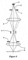
- FIGURE 2 shows the same principle of operation for a multi-beam system.
- a plurality of beamlets 9 passes consecutively a first aperture array 10, a first lens array 11, a deflector array 12, a second aperture array 13 that serves as beamlet stop array and a second lens array 14, which again focuses the transmitted beamlets 15 on an image plane 8.
- lens arrays also single lenses, arranged in one plane, can be used.
- the function of all these components is comparable with the equivalents in FIGURE 1 .
- the beamlets 9 may be created with a plurality of charged particle sources or by splitting a collimated charged particle beam emitted by a single charged particle source, for instance by means of an aperture plate.
- FIGURES 1 and 2 The concept depicted in FIGURES 1 and 2 is widely used, but it has a major disadvantage that especially becomes important when operating at high deflection frequencies.
- the spot on the second aperture 6 is not sharply defined. Its intensity fades away.
- the deflection angle needed to block the beamlets 16 completely is not well defined. Consequently a large deflection angle is needed to ensure the blocking operation.
- a small deflection angle is desired.
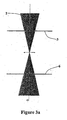
- FIGURE 3a shows an example of a correctly positioned deflector.
- the beamlet fills the area of both apertures.
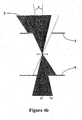
- Figure 4b shows the effect of the a slight rotation or the optical axis of beamlet 2 on the optical configuration of figure 4a : the heatload increases considerable.
- Figure 4c shows the effect of a shift in the optical axis of beamlet 2 from o to position o': again, the heat load on the second aperture increases. The heatload on the first aperture 3 also increases. Furthermore, the position of a beamlet on image plane 8 varies with the position of the optical axis of the beamlet, and with the angle of the optical axis of the beamlet.
- a simple enlargement of the opening angle has a major disadvantage though.
- the lens filling of the lens following the aperture with a larger opening angle increases. Consequently the performance of the lens deteriorates.
- FIGURE 5 and FIGURE 6 shows a first embodiment of the present invention for shows a single beam optical system which does not form part of the present invention, a multibeam electron optical system respectively.
- the first aperture 3 is placed in the conjugate plane of the second aperture 6.
- the filling of the first lens 4 is therefore reduced, which enhances its performance i.e. less aberrations are introduced.
- the spot on the second aperture 6 is sharp, which results in a well-defined deflection angle of the electrostatic deflector 5 to accomplish blocking of the passing charged particle beam.
- the heat load on the first aperture 3 becomes too large, several apertures elements are arranged in a serial order along the path of the charged particle beam.
- the aperture elements are then mutually aligned and preferably arranged in a serial order with decreasing diameter along the electron optical path.
- the beam-limiting aperture element is then imaged on the second aperture 6.
- the second aperture 6 also comprises a series of aperture elements, preferably with decreasing diameter along the electron optical path, the beam limiting aperture element of the first aperture 3 is projected on the beam limiting aperture element of the second aperture 6 by the first lens 4.
- this structure is implemented in the multibeam system according to the first embodiment of the present invention as depicted in FIGURE 6 .
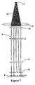
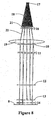
- FIGURE 7 shows such a single source multibeam electron optical system incorporated with the first embodiment of the present invention.
- a charged particle source 17 emits a diverging beam 18, which is collimated by a collimator lens 19 before reaching the first aperture array 10.
- the first aperture array 10 then splits the beam into a plurality of beamlets. The rest of the operation is similar to the operation of the system described with respect to FIGURE 6 .
- the collimator lens 19 introduces additional aberrations in the system.
- FIGURE 8 Details of this approach are disclosed in WO 2004/081910 .
- an additional lens array 20 is positioned between said collimator lens 19 and said charged particle source 17.
- a third aperture array 21 is placed between the lens array 20 and the source 17. Now the aperture array 21 splits the emitted charged particle beam 18 in a plurality of beamlets 22 and additionally takes care of the large heat load.
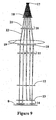
- FIGURE 9 shows the first embodiment of the present invention applied in the system depicted in FIGURE 8 .
- the position of the third aperture array 21 should be positioned in the conjugate plane of the first aperture array 10.
- the lens fillings of all lens arrays 11, 14, 20 are minimised, while the opening angles are large enough to deal with the position variations.
- the spot on the beamlet stop array 13 remains sharp, which leads to the capability to deflect with a high frequency due to the small minimum deflection angle.
Abstract
Description
- This invention relates to charged particle optical system for a charged particle exposure apparatus, in particular a maskless lithography system using charged particles.
- The development of lithography systems in particular is driven by Moore's law i.e. the number of transistors per unit area doubles every 18 months. Consequently the feature sizes decrease rapidly resulting in a sharp increase of the costs of a masks currently used for providing a pattern. To avoid the increasing mask costs several maskless lithography concepts are under development. In these concepts the pattern is represented by pattern data. Since a mask is a highly efficient way to store a pattern, the amount of raw data describing such a pattern is enormous.
- Current maskless lithography systems are limited in throughput, i.e. the number of processed wafers per hour. This feature limits the use of these systems in present day semiconductor element processing lines. The throughput of a maskless lithography system can be enhanced by using a plurality of beamlets and/or by increasing the data rate.
- The supply of data can be increased in two ways. A first way of increasing the data rate is by sending the pattern data directly to the beam source or sources, thus switching the source of sources on and off. Alternatively, the source or sources continuously emit one or more beamlets and the pattern data is provided to modulation means that modulate the emitted beamlets along their pathway towards the target to be patterned.
- The data supply to the sources becomes a problem when the data rate increases: Each individual source has a settling time that is source-dependent and becomes too large easily. It is therefore preferred to modulate the beamlets along their optical pathway.
- In charged particle beam lithography systems, these modulation means are often electrostatic deflection arrays, also known as blanking aperture arrays (BAA) or deflection arrays. Examples of such arrays are disclosed in
US-patent 6188074 by Advantest and inEP-patent application 1253619 by Canon. Upon the supply of an electric signal towards a certain deflection element, an electric field is established over a corresponding aperture, which results in the deflection of a charged particle beam passing through the aperture. By positioning an aperture plate behind the deflection array, wherein the apertures are aligned with apertures in the deflection array, the deflected beams are blocked and therefore do not reach the target. - Before the charged particles reach the deflection array, the beams most often pass an aperture array. This aperture array has several functions. In lithography systems comprising a single source it is used to split an emitted beam in a plurality of beamlets. Furthermore, it determines the opening angle of the beam at the deflection array. Additionally the aperture array reduces the heat load on the deflection array, thereby enhancing its performance.
- Especially in compact multibeam designs, misalignment of the consecutive components (lenses, apertures etc.) of the system or a slight change of the position of the beam by for instance external electromagnetic fields, for instance resulting from charging of surfaces or irregularities on charged surfaces, results in dose variations. As a result of the dose variation the control of the critical dimensions of the features to be patterned is no longer guaranteed. One way of dealing with misalignment problems is increasing the opening angle of each beamlet, i.e. making the cross section of a beamlet on an aperture array larger than the aperture which is passes. In that way, it is ensured that the entire area of an aperture is illuminated.
- This approach has several drawbacks, which become pertinent when high speed and extreme dose stability are required. The relatively large cross section will increase the heat load on an aperture array. Furthermore, the amount of deflection needed to completely block a beamlet will increase (see drawings for an explanation), which will reduce the speed and thus throughput of such a system. Also, for accurate dose control at the position of a substrate it is desired to approach a tophat distribution of the beam intensity as much as possible. A large opening angle of a beam causes a beam to have large tails.
- An example of a multi beam exposure apparatus is shown in
US 2002/0039829 A . This apparatus comprises first and second aperture arrays and a an array of lenses arranged between these aperture arrays to adjust the focus of beams formed by the first aperture array to the second aperture array, and further beam shaping deflection units to deflect each beam independently to a desired position on the second aperture array. - It is the purpose of the present device to provide a maskless charged particle lithography system with arrangements to overcome the aforementioned problems encountered in charged particle optical systems, in particular is such systems used in the present maskless charged particle multi-beam lithography systems. It thus seeks to provide a charged particle optical system which has an improved speed and stability.
- The invention therefore provides a charged particle beam exposure apparatus as defined in
claim 1. - It was found that imaging a previous aperture or aperture array on a subsequent aperture or aperture array makes the system more stable with respect to alignment, and reduces heat load.
- In this respect, with conjugate planes are meant planes formed by a plane on one side of a lens or lens system and its image plane at the other side of the lens or lens system by shielding or blocking.
- The invention will be further elucidated in the following embodiments of a charged particle beam exposure apparatus in particular for a maskless lithography system, according to the current invention, in which:
-
Figure 1 shows a cross-section of a charged particle optical system, -
Figure 1A shows a top view offigure 1 . -
figure 2 shows a cross-section of a multi-beamlet charged particle optical system, -
figures 3a-3d explain the problems, -
figures 4a-4c explain further problem, -
figure 5 shows a charged particle optical system for a single beam system, -
figure 6 shows a first embodiment of a charged particle optical system for a multibeam system according to the present invention, -
figure 7 shows a second embodiment of a charged particle optical system for a multibeam system according to the present invention, -
figure 8 shows a third embodiment of a charged particle optical system for a multi particle beam system according to the present invention, and -
figure 9 yet another embodiment of the system. -
FIGURE 1 shows cross section along the optical axis of a charged particle beam exposure apparatus comprising a charged particle source, two apertures, two lenses and one electrostatic deflector. TheFIGURE 1A shows a top-view ofFIGURE 1 - The
source 1 emits a divergingcharged particle beam 2. Thefirst aperture 3, being substantially round, limits the opening angle of the beam impinging on thefirst lens 4. Additionally it takes heat away from the system, thereby enhancing the performance of thefirst lens 4. Saidlens 4 focuses the beam substantially on the plane of theelectrostatic deflector 5. Upon the reception of control signals, thedeflector 5 deflects the passing charged particle beam. Thesecond aperture 6, being substantially round, can have several purposes. First of all it may limit the opening angle of the beam falling on thesecond lens 7. Secondly it blocks the beam when deflected by theelectrostatic deflector 5. When the beam is transmitted through thesecond aperture 6 thesecond lens 7 focuses it on animage plane 8. -
FIGURE 2 shows the same principle of operation for a multi-beam system. A plurality ofbeamlets 9 passes consecutively afirst aperture array 10, afirst lens array 11, adeflector array 12, asecond aperture array 13 that serves as beamlet stop array and asecond lens array 14, which again focuses the transmitted beamlets 15 on animage plane 8. Instead of lens arrays also single lenses, arranged in one plane, can be used. The function of all these components is comparable with the equivalents inFIGURE 1 . Thebeamlets 9 may be created with a plurality of charged particle sources or by splitting a collimated charged particle beam emitted by a single charged particle source, for instance by means of an aperture plate. - The concept depicted in
FIGURES 1 and2 is widely used, but it has a major disadvantage that especially becomes important when operating at high deflection frequencies. Considering the single beam system, the spot on thesecond aperture 6 is not sharply defined. Its intensity fades away. As a result the deflection angle needed to block thebeamlets 16 completely is not well defined. Consequently a large deflection angle is needed to ensure the blocking operation. However, at high deflection frequencies a small deflection angle is desired. - Additional problems arise in practice when the intermediate image created in the plane of the
electrostatic deflector 5 is not positioned correctly. -
FIGURE 3a shows an example of a correctly positioned deflector. The beamlet fills the area of both apertures. - In
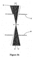
figure 3b , the effect of a having a slightly rotated angel A is demonstrated. In this case, a part ofbeamlet 2 is blocked by thefirst aperture 3. Therefore,aperture 6 is not completely filled, leading to dose variations. - In
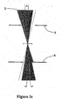
figure 3c , the area of thefirst aperture 3 is enlarged in an attempt to overcome the problem offigure 3b , and making the optical system less prone to variations in the angle of theincoming beamlet 2. In this case, however,beamlet 2 is partly blocked by thesecond aperture 6. This solution therefore does not solve the problem. - In
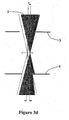
figure 3d , the effect of a small shift in the optical axis o from o -> o' is demonstrated. A known solution is to increase the area for the first aperture. Fromfigure 3d , however, it is clear that this does not solve the problem.Second aperture 6 still blocks part of thebeamlet 2. - In
figure 4a , in an attempt to make the system more stable, the opening angle ofbeamlet 2 is enlarged and thefirst aperture 3 is enlarged. In this situation, the heat load on thesecond aperture 6 increases as this aperture now blocks part of thebeamlet 2. Furthermore, to removebeamlet 2 completely from the aperture, thus blanking the beamlet usingaperture plate 6, requires a lager deflection angle, thus requiring a stronger electrostatic field. This makes the deflector more complex. Furthermore, it makes the deflector slower. -
Figure 4b shows the effect of the a slight rotation or the optical axis ofbeamlet 2 on the optical configuration offigure 4a : the heatload increases considerable. -
Figure 4c shows the effect of a shift in the optical axis ofbeamlet 2 from o to position o': again, the heat load on the second aperture increases. The heatload on thefirst aperture 3 also increases. Furthermore, the position of a beamlet onimage plane 8 varies with the position of the optical axis of the beamlet, and with the angle of the optical axis of the beamlet. - As a result of the position variations the current passing through the apertures is different for each individual aperture. Consequently the current arriving at the
image plane 8 varies per chargedparticle beamlet 15. When a surface to be exposed, for instance a semiconductor wafer or a photo mask, is positioned in saidimage plane 8, the current variations result in dose variations i.e. variations in the number of charged particles per unit area. Due to these dose variations the critical dimension control of a pattern with high-resolution features is no longer possible. A method to reduce the negative influences of position variations is to enlarge the opening angle falling on the apertures as is shown inFIGURE 4b and4c . Although part of the current is "thrown away" each individual aperture now transmits a similar area of an individual charged particle beamlet. - An additional problem caused by position variations of the beam spot at the apertures is the following. Since the source is not a singularity but has a finite size, the current distribution within each beamlet is not homogeneous. At the periphery of the beamlet the current density becomes smaller. So the solution demonstrated in
FIGURE 4a does not completely solve the problems. Consequently the opening angle should be enlarged even further than before, such that the transmitted part of the beamlet only comprises a part of the centre region with a homogeneous current density. In this way the non-homogeneity effect is compensated for. - A simple enlargement of the opening angle has a major disadvantage though. The lens filling of the lens following the aperture with a larger opening angle increases. Consequently the performance of the lens deteriorates. It is the purpose of the present invention to provide a electron optical system wherein the maximum opening angle needed to avoid aforementioned problems with position variations is minimised. Additionally the present invention enables the use of a small deflection angle to block a passing beam or beamlet upon the registration of a control signal.
-
FIGURE 5 andFIGURE 6 shows a first embodiment of the present invention for shows a single beam optical system which does not form part of the present invention, a multibeam electron optical system respectively. InFIGURE 5 thefirst aperture 3 is placed in the conjugate plane of thesecond aperture 6. As a result the required opening angle determined by thefirst aperture 3 to minimise the influence of position variations is smaller than before. The filling of thefirst lens 4 is therefore reduced, which enhances its performance i.e. less aberrations are introduced. Moreover the spot on thesecond aperture 6 is sharp, which results in a well-defined deflection angle of theelectrostatic deflector 5 to accomplish blocking of the passing charged particle beam. If the heat load on thefirst aperture 3 becomes too large, several apertures elements are arranged in a serial order along the path of the charged particle beam. The aperture elements are then mutually aligned and preferably arranged in a serial order with decreasing diameter along the electron optical path. In this case the beam-limiting aperture element is then imaged on thesecond aperture 6. When thesecond aperture 6 also comprises a series of aperture elements, preferably with decreasing diameter along the electron optical path, the beam limiting aperture element of thefirst aperture 3 is projected on the beam limiting aperture element of thesecond aperture 6 by thefirst lens 4. In a similar fashion this structure is implemented in the multibeam system according to the first embodiment of the present invention as depicted inFIGURE 6 . - The second embodiment of the present invention is only applicable for multibeam systems, especially the systems comprising a single source.
FIGURE 7 shows such a single source multibeam electron optical system incorporated with the first embodiment of the present invention. A chargedparticle source 17 emits a divergingbeam 18, which is collimated by acollimator lens 19 before reaching thefirst aperture array 10. Thefirst aperture array 10 then splits the beam into a plurality of beamlets. The rest of the operation is similar to the operation of the system described with respect toFIGURE 6 . Thecollimator lens 19 introduces additional aberrations in the system. - To reduce these aberrations the system can be adapted as shown in
FIGURE 8 . Details of this approach are disclosed inWO 2004/081910 . In this configuration anadditional lens array 20 is positioned between saidcollimator lens 19 and said chargedparticle source 17. To avoid significant heating of theadditional lens array 20, thereby degrading its performance, athird aperture array 21 is placed between thelens array 20 and thesource 17. Now theaperture array 21 splits the emitted chargedparticle beam 18 in a plurality ofbeamlets 22 and additionally takes care of the large heat load. -
FIGURE 9 shows the first embodiment of the present invention applied in the system depicted inFIGURE 8 . Following the same reasoning as with the first embodiment regarding position variations, the position of thethird aperture array 21 should be positioned in the conjugate plane of thefirst aperture array 10. The lens fillings of alllens arrays beamlet stop array 13 remains sharp, which leads to the capability to deflect with a high frequency due to the small minimum deflection angle.
Claims (2)
- A charged particle beam exposure apparatus using a plurality of charged particle beamlets (9), said apparatus comprising:- a first aperture means (10) comprising a plurality of first substantially round apertures for partially shielding a charged particle beamlet;- a first lens system (11) comprising a plurality of lenses for focusing said charged particle beamlets, originating from said first aperture, within or in the vicinity of an image focal plane of said lenses;- a deflector means (12) comprising a plurality of beamlet deflectors for the deflection of said charged particle beamlets passing said deflector upon the reception of a control signal,- a second aperture means (13) comprising a plurality of substantially round apertures positioned in the conjugate plane of the first aperture means, said second apertures being aligned with said first apertures and said beamlet deflectors for blocking said charged particle beamlets upon deflection by said beamlet deflectors and to transmit it otherwise, and wherein the first and second apertures are positioned for limiting the opening angle of the beamlet when looking in upstream direction of said beamlet, and- a second lens array (14) comprising a plurality of lenses in one plane for focusing the transmitted beamlets on an image plane (8) in which, in use, a surface to be exposed is positioned, wherein the deflector means (12) with respect to the second lens array (14) is arranged in a conjugate plane of the image plane (8).
- Charged particle beam exposure apparatus according to claim 1, wherein the deflector means (12) is substantially located in said image focal plane.
Applications Claiming Priority (2)
| Application Number | Priority Date | Filing Date | Title |
|---|---|---|---|
| US47381003P | 2003-05-28 | 2003-05-28 | |
| EP04748613A EP1627412B1 (en) | 2003-05-28 | 2004-05-27 | Charged particle beamlet exposure system |
Related Parent Applications (2)
| Application Number | Title | Priority Date | Filing Date |
|---|---|---|---|
| EP04748613.9 Division | 2004-05-27 | ||
| EP04748613A Division EP1627412B1 (en) | 2003-05-28 | 2004-05-27 | Charged particle beamlet exposure system |
Publications (3)
| Publication Number | Publication Date |
|---|---|
| EP1830384A2 EP1830384A2 (en) | 2007-09-05 |
| EP1830384A3 EP1830384A3 (en) | 2007-09-19 |
| EP1830384B1 true EP1830384B1 (en) | 2011-09-14 |
Family
ID=33490650
Family Applications (2)
| Application Number | Title | Priority Date | Filing Date |
|---|---|---|---|
| EP04748613A Active EP1627412B1 (en) | 2003-05-28 | 2004-05-27 | Charged particle beamlet exposure system |
| EP07075242A Active EP1830384B1 (en) | 2003-05-28 | 2004-05-27 | Charged particle beamlet exposure system |
Family Applications Before (1)
| Application Number | Title | Priority Date | Filing Date |
|---|---|---|---|
| EP04748613A Active EP1627412B1 (en) | 2003-05-28 | 2004-05-27 | Charged particle beamlet exposure system |
Country Status (8)
| Country | Link |
|---|---|
| US (1) | US7084414B2 (en) |
| EP (2) | EP1627412B1 (en) |
| JP (1) | JP4949843B2 (en) |
| KR (2) | KR101175523B1 (en) |
| CN (1) | CN100543920C (en) |
| AT (2) | ATE524822T1 (en) |
| DE (1) | DE602004005704T2 (en) |
| WO (1) | WO2004107050A2 (en) |
Families Citing this family (62)
| Publication number | Priority date | Publication date | Assignee | Title |
|---|---|---|---|---|
| US7928404B2 (en) * | 2003-10-07 | 2011-04-19 | Multibeam Corporation | Variable-ratio double-deflection beam blanker |
| US20090008579A1 (en) * | 2003-10-07 | 2009-01-08 | Tokyo Electron Limited | Electron beam lithography apparatus and design method of patterned beam-defining aperture |
| US7462848B2 (en) * | 2003-10-07 | 2008-12-09 | Multibeam Systems, Inc. | Optics for generation of high current density patterned charged particle beams |
| CN101019203B (en) * | 2004-05-17 | 2010-12-22 | 迈普尔平版印刷Ip有限公司 | Charged particle beam exposure system |
| US7425713B2 (en) * | 2005-01-14 | 2008-09-16 | Arradiance, Inc. | Synchronous raster scanning lithographic system |
| NL1029132C2 (en) * | 2005-05-26 | 2006-11-28 | Univ Delft Tech | Device for generating parallel ray-beam parts. |
| US8597089B2 (en) * | 2005-07-08 | 2013-12-03 | Praxair Technology, Inc. | System and method for treating live cargo such as poultry with gas |
| US20090256075A1 (en) * | 2005-09-06 | 2009-10-15 | Carl Zeiss Smt Ag | Charged Particle Inspection Method and Charged Particle System |
| JP2009531855A (en) * | 2006-03-27 | 2009-09-03 | マルチビーム システムズ インコーポレイテッド | Optical system for generating high current density patterned charged particle beams |
| US7781748B2 (en) * | 2006-04-03 | 2010-08-24 | Ims Nanofabrication Ag | Particle-beam exposure apparatus with overall-modulation of a patterned beam |
| US8134135B2 (en) | 2006-07-25 | 2012-03-13 | Mapper Lithography Ip B.V. | Multiple beam charged particle optical system |
| US7569834B1 (en) | 2006-10-18 | 2009-08-04 | Kla-Tencor Technologies Corporation | High resolution charged particle projection lens array using magnetic elements |
| EP2019415B1 (en) * | 2007-07-24 | 2016-05-11 | IMS Nanofabrication AG | Multi-beam source |
| US8890094B2 (en) | 2008-02-26 | 2014-11-18 | Mapper Lithography Ip B.V. | Projection lens arrangement |
| US8445869B2 (en) | 2008-04-15 | 2013-05-21 | Mapper Lithography Ip B.V. | Projection lens arrangement |
| KR101638766B1 (en) | 2008-04-15 | 2016-07-13 | 마퍼 리쏘그라피 아이피 비.브이. | Beamlet blanker arrangement |
| US7851774B2 (en) * | 2008-04-25 | 2010-12-14 | Taiwan Semiconductor Manufacturing Company, Ltd. | System and method for direct writing to a wafer |
| CN102105960B (en) * | 2008-05-23 | 2014-01-29 | 迈普尔平版印刷Ip有限公司 | Imaging system |
| EP2128885A1 (en) * | 2008-05-26 | 2009-12-02 | FEI Company | Charged particle source with integrated energy filter |
| KR101687955B1 (en) | 2009-02-22 | 2016-12-20 | 마퍼 리쏘그라피 아이피 비.브이. | Charged particle lithography apparatus and method of generating vacuum in a vacuum chamber |
| CN102414775A (en) | 2009-02-22 | 2012-04-11 | 迈普尔平版印刷Ip有限公司 | Method and arrangement for realizing vacuum in vacuum chamber |
| JP5539406B2 (en) | 2009-02-22 | 2014-07-02 | マッパー・リソグラフィー・アイピー・ビー.ブイ. | Lithography machine and substrate processing structure |
| KR101545193B1 (en) * | 2009-02-22 | 2015-08-18 | 마퍼 리쏘그라피 아이피 비.브이. | Charged particle lithography apparatus and method of generating vacuum in a vacuum chamber |
| KR101614460B1 (en) | 2009-05-20 | 2016-04-21 | 마퍼 리쏘그라피 아이피 비.브이. | Pattern data conversion for lithography system |
| KR101605832B1 (en) * | 2009-05-20 | 2016-03-23 | 마퍼 리쏘그라피 아이피 비.브이. | Method of generating a two-level pattern for lithographic processing and pattern generator using the same |
| EP3144955A1 (en) | 2009-05-20 | 2017-03-22 | Mapper Lithography IP B.V. | Method for exposing a wafer |
| CN102687232A (en) | 2009-10-26 | 2012-09-19 | 迈普尔平版印刷Ip有限公司 | Modulation device and charged particle multi-beamlet lithography system |
| US8952342B2 (en) * | 2009-12-17 | 2015-02-10 | Mapper Lithography Ip B.V. | Support and positioning structure, semiconductor equipment system and method for positioning |
| TWI534852B (en) | 2010-10-26 | 2016-05-21 | 瑪波微影Ip公司 | Lithography system, modulation device and method of manufacturing a fiber fixation substrate |
| TWI517196B (en) | 2010-11-13 | 2016-01-11 | 瑪波微影Ip公司 | Charged particle lithography system with intermediate chamber |
| KR101755577B1 (en) | 2010-11-13 | 2017-07-07 | 마퍼 리쏘그라피 아이피 비.브이. | Charged particle lithography system with aperture array cooling |
| US8604411B2 (en) | 2010-11-13 | 2013-12-10 | Mapper Lithography Ip B.V. | Charged particle beam modulator |
| US8884255B2 (en) | 2010-11-13 | 2014-11-11 | Mapper Lithography Ip B.V. | Data path for lithography apparatus |
| US9305747B2 (en) | 2010-11-13 | 2016-04-05 | Mapper Lithography Ip B.V. | Data path for lithography apparatus |
| JP6158091B2 (en) | 2010-12-14 | 2017-07-05 | マッパー・リソグラフィー・アイピー・ビー.ブイ. | Lithographic system and method for processing a substrate in such a lithographic system |
| JP5902201B2 (en) | 2011-02-16 | 2016-04-13 | マッパー・リソグラフィー・アイピー・ビー.ブイ. | Magnetic shielding system |
| RU2573398C2 (en) | 2011-04-22 | 2016-01-20 | МЭППЕР ЛИТОГРАФИ АйПи Б.В. | Network architecture and protocol for cluster of patterning machines |
| TWI514089B (en) * | 2011-04-28 | 2015-12-21 | Mapper Lithography Ip Bv | Apparatus for transferring a substrate in a lithography system |
| RU2014114517A (en) | 2011-09-12 | 2015-10-20 | МЭППЕР ЛИТОГРАФИ АйПи Б.В. | DEVICE PROCESSING DEVICE |
| WO2013045636A2 (en) | 2011-09-28 | 2013-04-04 | Mapper Lithography Ip B.V. | Plasma generator |
| JP2015509666A (en) | 2012-03-08 | 2015-03-30 | マッパー・リソグラフィー・アイピー・ビー.ブイ. | Charged particle lithography system with alignment sensor and beam measurement sensor |
| KR102069183B1 (en) | 2012-03-20 | 2020-01-22 | 에이에스엠엘 네델란즈 비.브이. | Arrangement and method for transporting radicals |
| KR101945964B1 (en) | 2012-05-14 | 2019-02-11 | 마퍼 리쏘그라피 아이피 비.브이. | Charged particle multi-beamlet lithography system and cooling arrangement manufacturing method |
| NL2010759C2 (en) | 2012-05-14 | 2015-08-25 | Mapper Lithography Ip Bv | Modulation device and power supply arrangement. |
| US10586625B2 (en) | 2012-05-14 | 2020-03-10 | Asml Netherlands B.V. | Vacuum chamber arrangement for charged particle beam generator |
| US11348756B2 (en) | 2012-05-14 | 2022-05-31 | Asml Netherlands B.V. | Aberration correction in charged particle system |
| US9653261B2 (en) | 2012-05-14 | 2017-05-16 | Mapper Lithography Ip B.V. | Charged particle lithography system and beam generator |
| NL2010760C2 (en) | 2013-05-03 | 2014-11-04 | Mapper Lithography Ip Bv | Beam grid layout. |
| EP2816585A1 (en) * | 2013-06-17 | 2014-12-24 | ICT Integrated Circuit Testing Gesellschaft für Halbleiterprüftechnik mbH | Charged particle beam system and method of operating thereof |
| US9922801B2 (en) | 2013-08-23 | 2018-03-20 | Mapper Lithography Ip B.V. | Drying apparatus for use in a lithography system |
| TWI641017B (en) | 2013-11-14 | 2018-11-11 | Asml Netherlands B.V. | Collimator electrode stack and charged particle lithography system |
| WO2015101537A1 (en) | 2013-12-30 | 2015-07-09 | Mapper Lithography Ip B.V. | Cathode arrangement, electron gun, and lithography system comprising such electron gun |
| EP3218926A2 (en) | 2014-11-14 | 2017-09-20 | Mapper Lithography IP B.V. | Load lock system and method for transferring substrates in a lithography system |
| US9484188B2 (en) | 2015-03-11 | 2016-11-01 | Mapper Lithography Ip B.V. | Individual beam pattern placement verification in multiple beam lithography |
| US10096450B2 (en) | 2015-12-28 | 2018-10-09 | Mapper Lithography Ip B.V. | Control system and method for lithography apparatus |
| US9981293B2 (en) | 2016-04-21 | 2018-05-29 | Mapper Lithography Ip B.V. | Method and system for the removal and/or avoidance of contamination in charged particle beam systems |
| KR102401179B1 (en) * | 2017-12-12 | 2022-05-24 | 삼성전자주식회사 | Aperture system of electron beam apparatus, electron beam exposure apparatus, and electron beam exposure apparatus system |
| US11164716B2 (en) * | 2018-03-29 | 2021-11-02 | Hitachi High-Tech Corporation | Charged particle beam device |
| JP2021532545A (en) * | 2018-08-09 | 2021-11-25 | エーエスエムエル ネザーランズ ビー.ブイ. | Device for multiple charged particle beams |
| NL2022156B1 (en) | 2018-12-10 | 2020-07-02 | Asml Netherlands Bv | Plasma source control circuit |
| KR20210096657A (en) * | 2018-12-31 | 2021-08-05 | 에이에스엠엘 네델란즈 비.브이. | Systems and methods for real-time stereo imaging using multiple electron beams |
| US11651934B2 (en) | 2021-09-30 | 2023-05-16 | Kla Corporation | Systems and methods of creating multiple electron beams |
Family Cites Families (15)
| Publication number | Priority date | Publication date | Assignee | Title |
|---|---|---|---|---|
| US4243866A (en) | 1979-01-11 | 1981-01-06 | International Business Machines Corporation | Method and apparatus for forming a variable size electron beam |
| US4543512A (en) | 1980-10-15 | 1985-09-24 | Tokyo Shibaura Denki Kabushiki Kaisha | Electron beam exposure system |
| US4544847A (en) * | 1983-07-28 | 1985-10-01 | Varian Associates, Inc. | Multi-gap magnetic imaging lens for charged particle beams |
| JPS6142132A (en) * | 1984-08-06 | 1986-02-28 | Nippon Telegr & Teleph Corp <Ntt> | Charged beam exposure apparatus |
| JPH097538A (en) * | 1995-06-26 | 1997-01-10 | Nippon Telegr & Teleph Corp <Ntt> | Charged beam drawing device |
| JP3908294B2 (en) * | 1996-02-02 | 2007-04-25 | 富士通株式会社 | Electron beam exposure apparatus and electron beam exposure method for reducing current amount of electron beam |
| US5912469A (en) * | 1996-07-11 | 1999-06-15 | Nikon Corporation | Charged-particle-beam microlithography apparatus |
| KR19990062942A (en) | 1997-12-10 | 1999-07-26 | 히로시 오우라 | Charge particle beam exposure device |
| US6014200A (en) * | 1998-02-24 | 2000-01-11 | Nikon Corporation | High throughput electron beam lithography system |
| JP4578606B2 (en) * | 2000-02-09 | 2010-11-10 | 富士通セミコンダクター株式会社 | Charged particle beam drawing apparatus and charged particle beam size adjusting method |
| US6651513B2 (en) | 2000-04-27 | 2003-11-25 | Endress + Hauser Flowtec Ag | Vibration meter and method of measuring a viscosity of a fluid |
| JP4601146B2 (en) * | 2000-10-03 | 2010-12-22 | 株式会社アドバンテスト | Electron beam exposure system |
| JP4112791B2 (en) * | 2000-10-03 | 2008-07-02 | 株式会社アドバンテスト | Electron beam correction method and electron beam exposure apparatus |
| JP2002217089A (en) * | 2001-01-18 | 2002-08-02 | Advantest Corp | Electron beam deflector, its manufacturing method and electron beam aligner |
| JP4647820B2 (en) * | 2001-04-23 | 2011-03-09 | キヤノン株式会社 | Charged particle beam drawing apparatus and device manufacturing method |
-
2004
- 2004-05-27 AT AT07075242T patent/ATE524822T1/en active
- 2004-05-27 CN CNB2004800145787A patent/CN100543920C/en active Active
- 2004-05-27 US US10/856,050 patent/US7084414B2/en not_active Expired - Fee Related
- 2004-05-27 KR KR1020127003554A patent/KR101175523B1/en active IP Right Grant
- 2004-05-27 AT AT04748613T patent/ATE358885T1/en active
- 2004-05-27 WO PCT/NL2004/000381 patent/WO2004107050A2/en active IP Right Grant
- 2004-05-27 EP EP04748613A patent/EP1627412B1/en active Active
- 2004-05-27 DE DE602004005704T patent/DE602004005704T2/en active Active
- 2004-05-27 KR KR1020057022719A patent/KR101168200B1/en active IP Right Grant
- 2004-05-27 EP EP07075242A patent/EP1830384B1/en active Active
- 2004-05-27 JP JP2006532135A patent/JP4949843B2/en not_active Expired - Fee Related
Also Published As
| Publication number | Publication date |
|---|---|
| KR20120025629A (en) | 2012-03-15 |
| CN1795529A (en) | 2006-06-28 |
| KR101168200B1 (en) | 2012-07-25 |
| EP1627412B1 (en) | 2007-04-04 |
| WO2004107050A3 (en) | 2005-04-21 |
| JP2007500948A (en) | 2007-01-18 |
| EP1627412A2 (en) | 2006-02-22 |
| KR101175523B1 (en) | 2012-08-21 |
| EP1830384A3 (en) | 2007-09-19 |
| EP1830384A2 (en) | 2007-09-05 |
| ATE358885T1 (en) | 2007-04-15 |
| CN100543920C (en) | 2009-09-23 |
| JP4949843B2 (en) | 2012-06-13 |
| US20050161621A1 (en) | 2005-07-28 |
| DE602004005704D1 (en) | 2007-05-16 |
| WO2004107050A2 (en) | 2004-12-09 |
| KR20060036391A (en) | 2006-04-28 |
| ATE524822T1 (en) | 2011-09-15 |
| DE602004005704T2 (en) | 2007-12-27 |
| US7084414B2 (en) | 2006-08-01 |
Similar Documents
| Publication | Publication Date | Title |
|---|---|---|
| EP1830384B1 (en) | Charged particle beamlet exposure system | |
| TWI534849B (en) | Projection lens arrangement | |
| JP4995261B2 (en) | Particle beam exposure system with total modulation of patterned beam | |
| US5831270A (en) | Magnetic deflectors and charged-particle-beam lithography systems incorporating same | |
| KR101900050B1 (en) | Muli-charged particle beam apparatus | |
| EP1602121B1 (en) | Apparatus for generating a plurality of beamlets | |
| US6472672B1 (en) | Electron beam exposure apparatus and its control method | |
| EP3020062B1 (en) | Beam grid layout | |
| EP2019415B1 (en) | Multi-beam source | |
| KR20110030466A (en) | Imaging system | |
| US6145438A (en) | Method and apparatus for direct writing of semiconductor die using microcolumn array | |
| KR102025602B1 (en) | Aperture set for multi beam and multi-charged particle beam writing apparatus | |
| JP3983772B2 (en) | Charged particle beam application equipment | |
| KR102468349B1 (en) | Aperture substrate set for multi-beam and multi-charged particle beam writing apparatus | |
| JP2006080304A (en) | Charged particle beam exposure apparatus | |
| US6023067A (en) | Blanking system for electron beam projection system | |
| JP2005203464A (en) | Charged particle beam exposure device | |
| WO2002103764A1 (en) | Electron beam exposure system | |
| JP2004153294A (en) | Electron beam exposure device, electron beam exposure method and device manufacturing method |
Legal Events
| Date | Code | Title | Description |
|---|---|---|---|
| PUAI | Public reference made under article 153(3) epc to a published international application that has entered the european phase |
Free format text: ORIGINAL CODE: 0009012 |
|
| PUAL | Search report despatched |
Free format text: ORIGINAL CODE: 0009013 |
|
| AC | Divisional application: reference to earlier application |
Ref document number: 1627412 Country of ref document: EP Kind code of ref document: P |
|
| AK | Designated contracting states |
Kind code of ref document: A2 Designated state(s): AT BE BG CH CY CZ DE DK EE ES FI FR GB GR HU IE IT LI LU MC NL PL PT RO SE SI SK TR |
|
| AK | Designated contracting states |
Kind code of ref document: A3 Designated state(s): AT BE BG CH CY CZ DE DK EE ES FI FR GB GR HU IE IT LI LU MC NL PL PT RO SE SI SK TR |
|
| 17P | Request for examination filed |
Effective date: 20080304 |
|
| 17Q | First examination report despatched |
Effective date: 20080425 |
|
| AKX | Designation fees paid |
Designated state(s): AT BE BG CH CY CZ DE DK EE ES FI FR GB GR HU IE IT LI LU MC NL PL PT RO SE SI SK TR |
|
| R17C | First examination report despatched (corrected) |
Effective date: 20090708 |
|
| GRAP | Despatch of communication of intention to grant a patent |
Free format text: ORIGINAL CODE: EPIDOSNIGR1 |
|
| RIN1 | Information on inventor provided before grant (corrected) |
Inventor name: KRUIT, PIETER Inventor name: WIELAND, MARCO JAN-JACO |
|
| GRAS | Grant fee paid |
Free format text: ORIGINAL CODE: EPIDOSNIGR3 |
|
| GRAA | (expected) grant |
Free format text: ORIGINAL CODE: 0009210 |
|
| AC | Divisional application: reference to earlier application |
Ref document number: 1627412 Country of ref document: EP Kind code of ref document: P |
|
| AK | Designated contracting states |
Kind code of ref document: B1 Designated state(s): AT BE BG CH CY CZ DE DK EE ES FI FR GB GR HU IE IT LI LU MC NL PL PT RO SE SI SK TR |
|
| REG | Reference to a national code |
Ref country code: CH Ref legal event code: EP |
|
| REG | Reference to a national code |
Ref country code: IE Ref legal event code: FG4D |
|
| REG | Reference to a national code |
Ref country code: DE Ref legal event code: R096 Ref document number: 602004034393 Country of ref document: DE Effective date: 20111124 |
|
| REG | Reference to a national code |
Ref country code: CH Ref legal event code: NV Representative=s name: E. BLUM & CO. AG PATENT- UND MARKENANWAELTE VSP |
|
| REG | Reference to a national code |
Ref country code: SE Ref legal event code: TRGR |
|
| REG | Reference to a national code |
Ref country code: NL Ref legal event code: T3 |
|
| PG25 | Lapsed in a contracting state [announced via postgrant information from national office to epo] |
Ref country code: FI Free format text: LAPSE BECAUSE OF FAILURE TO SUBMIT A TRANSLATION OF THE DESCRIPTION OR TO PAY THE FEE WITHIN THE PRESCRIBED TIME-LIMIT Effective date: 20110914 |
|
| PG25 | Lapsed in a contracting state [announced via postgrant information from national office to epo] |
Ref country code: CY Free format text: LAPSE BECAUSE OF FAILURE TO SUBMIT A TRANSLATION OF THE DESCRIPTION OR TO PAY THE FEE WITHIN THE PRESCRIBED TIME-LIMIT Effective date: 20110914 Ref country code: SI Free format text: LAPSE BECAUSE OF FAILURE TO SUBMIT A TRANSLATION OF THE DESCRIPTION OR TO PAY THE FEE WITHIN THE PRESCRIBED TIME-LIMIT Effective date: 20110914 Ref country code: GR Free format text: LAPSE BECAUSE OF FAILURE TO SUBMIT A TRANSLATION OF THE DESCRIPTION OR TO PAY THE FEE WITHIN THE PRESCRIBED TIME-LIMIT Effective date: 20111215 |
|
| PG25 | Lapsed in a contracting state [announced via postgrant information from national office to epo] |
Ref country code: SK Free format text: LAPSE BECAUSE OF FAILURE TO SUBMIT A TRANSLATION OF THE DESCRIPTION OR TO PAY THE FEE WITHIN THE PRESCRIBED TIME-LIMIT Effective date: 20110914 Ref country code: CZ Free format text: LAPSE BECAUSE OF FAILURE TO SUBMIT A TRANSLATION OF THE DESCRIPTION OR TO PAY THE FEE WITHIN THE PRESCRIBED TIME-LIMIT Effective date: 20110914 |
|
| PG25 | Lapsed in a contracting state [announced via postgrant information from national office to epo] |
Ref country code: PL Free format text: LAPSE BECAUSE OF FAILURE TO SUBMIT A TRANSLATION OF THE DESCRIPTION OR TO PAY THE FEE WITHIN THE PRESCRIBED TIME-LIMIT Effective date: 20110914 Ref country code: PT Free format text: LAPSE BECAUSE OF FAILURE TO SUBMIT A TRANSLATION OF THE DESCRIPTION OR TO PAY THE FEE WITHIN THE PRESCRIBED TIME-LIMIT Effective date: 20120116 Ref country code: RO Free format text: LAPSE BECAUSE OF FAILURE TO SUBMIT A TRANSLATION OF THE DESCRIPTION OR TO PAY THE FEE WITHIN THE PRESCRIBED TIME-LIMIT Effective date: 20110914 Ref country code: EE Free format text: LAPSE BECAUSE OF FAILURE TO SUBMIT A TRANSLATION OF THE DESCRIPTION OR TO PAY THE FEE WITHIN THE PRESCRIBED TIME-LIMIT Effective date: 20110914 |
|
| PLBE | No opposition filed within time limit |
Free format text: ORIGINAL CODE: 0009261 |
|
| STAA | Information on the status of an ep patent application or granted ep patent |
Free format text: STATUS: NO OPPOSITION FILED WITHIN TIME LIMIT |
|
| PG25 | Lapsed in a contracting state [announced via postgrant information from national office to epo] |
Ref country code: DK Free format text: LAPSE BECAUSE OF FAILURE TO SUBMIT A TRANSLATION OF THE DESCRIPTION OR TO PAY THE FEE WITHIN THE PRESCRIBED TIME-LIMIT Effective date: 20110914 |
|
| 26N | No opposition filed |
Effective date: 20120615 |
|
| REG | Reference to a national code |
Ref country code: DE Ref legal event code: R097 Ref document number: 602004034393 Country of ref document: DE Effective date: 20120615 |
|
| PG25 | Lapsed in a contracting state [announced via postgrant information from national office to epo] |
Ref country code: MC Free format text: LAPSE BECAUSE OF NON-PAYMENT OF DUE FEES Effective date: 20120531 |
|
| PG25 | Lapsed in a contracting state [announced via postgrant information from national office to epo] |
Ref country code: ES Free format text: LAPSE BECAUSE OF FAILURE TO SUBMIT A TRANSLATION OF THE DESCRIPTION OR TO PAY THE FEE WITHIN THE PRESCRIBED TIME-LIMIT Effective date: 20111225 |
|
| PG25 | Lapsed in a contracting state [announced via postgrant information from national office to epo] |
Ref country code: BG Free format text: LAPSE BECAUSE OF FAILURE TO SUBMIT A TRANSLATION OF THE DESCRIPTION OR TO PAY THE FEE WITHIN THE PRESCRIBED TIME-LIMIT Effective date: 20111214 |
|
| PG25 | Lapsed in a contracting state [announced via postgrant information from national office to epo] |
Ref country code: TR Free format text: LAPSE BECAUSE OF FAILURE TO SUBMIT A TRANSLATION OF THE DESCRIPTION OR TO PAY THE FEE WITHIN THE PRESCRIBED TIME-LIMIT Effective date: 20110914 |
|
| PG25 | Lapsed in a contracting state [announced via postgrant information from national office to epo] |
Ref country code: LU Free format text: LAPSE BECAUSE OF NON-PAYMENT OF DUE FEES Effective date: 20120527 |
|
| PG25 | Lapsed in a contracting state [announced via postgrant information from national office to epo] |
Ref country code: HU Free format text: LAPSE BECAUSE OF FAILURE TO SUBMIT A TRANSLATION OF THE DESCRIPTION OR TO PAY THE FEE WITHIN THE PRESCRIBED TIME-LIMIT Effective date: 20040527 |
|
| PGFP | Annual fee paid to national office [announced via postgrant information from national office to epo] |
Ref country code: GB Payment date: 20140519 Year of fee payment: 11 |
|
| PGFP | Annual fee paid to national office [announced via postgrant information from national office to epo] |
Ref country code: CH Payment date: 20140508 Year of fee payment: 11 Ref country code: IT Payment date: 20140527 Year of fee payment: 11 |
|
| REG | Reference to a national code |
Ref country code: CH Ref legal event code: PL |
|
| GBPC | Gb: european patent ceased through non-payment of renewal fee |
Effective date: 20150527 |
|
| PG25 | Lapsed in a contracting state [announced via postgrant information from national office to epo] |
Ref country code: CH Free format text: LAPSE BECAUSE OF NON-PAYMENT OF DUE FEES Effective date: 20150531 Ref country code: IT Free format text: LAPSE BECAUSE OF NON-PAYMENT OF DUE FEES Effective date: 20150527 Ref country code: LI Free format text: LAPSE BECAUSE OF NON-PAYMENT OF DUE FEES Effective date: 20150531 |
|
| PG25 | Lapsed in a contracting state [announced via postgrant information from national office to epo] |
Ref country code: GB Free format text: LAPSE BECAUSE OF NON-PAYMENT OF DUE FEES Effective date: 20150527 |
|
| REG | Reference to a national code |
Ref country code: FR Ref legal event code: PLFP Year of fee payment: 13 |
|
| PGFP | Annual fee paid to national office [announced via postgrant information from national office to epo] |
Ref country code: SE Payment date: 20160419 Year of fee payment: 13 Ref country code: BE Payment date: 20160426 Year of fee payment: 13 |
|
| REG | Reference to a national code |
Ref country code: FR Ref legal event code: PLFP Year of fee payment: 14 |
|
| PGFP | Annual fee paid to national office [announced via postgrant information from national office to epo] |
Ref country code: NL Payment date: 20170504 Year of fee payment: 14 |
|
| REG | Reference to a national code |
Ref country code: SE Ref legal event code: EUG |
|
| PG25 | Lapsed in a contracting state [announced via postgrant information from national office to epo] |
Ref country code: SE Free format text: LAPSE BECAUSE OF NON-PAYMENT OF DUE FEES Effective date: 20170528 |
|
| REG | Reference to a national code |
Ref country code: BE Ref legal event code: MM Effective date: 20170531 |
|
| REG | Reference to a national code |
Ref country code: FR Ref legal event code: PLFP Year of fee payment: 15 |
|
| PG25 | Lapsed in a contracting state [announced via postgrant information from national office to epo] |
Ref country code: BE Free format text: LAPSE BECAUSE OF NON-PAYMENT OF DUE FEES Effective date: 20170531 |
|
| REG | Reference to a national code |
Ref country code: NL Ref legal event code: MM Effective date: 20180601 |
|
| PG25 | Lapsed in a contracting state [announced via postgrant information from national office to epo] |
Ref country code: NL Free format text: LAPSE BECAUSE OF NON-PAYMENT OF DUE FEES Effective date: 20180601 |
|
| PGFP | Annual fee paid to national office [announced via postgrant information from national office to epo] |
Ref country code: IE Payment date: 20220518 Year of fee payment: 19 Ref country code: FR Payment date: 20220526 Year of fee payment: 19 Ref country code: DE Payment date: 20220527 Year of fee payment: 19 |
|
| PGFP | Annual fee paid to national office [announced via postgrant information from national office to epo] |
Ref country code: AT Payment date: 20220518 Year of fee payment: 19 |
|
| REG | Reference to a national code |
Ref country code: DE Ref legal event code: R119 Ref document number: 602004034393 Country of ref document: DE |
|
| REG | Reference to a national code |
Ref country code: AT Ref legal event code: MM01 Ref document number: 524822 Country of ref document: AT Kind code of ref document: T Effective date: 20230527 |
|
| PG25 | Lapsed in a contracting state [announced via postgrant information from national office to epo] |
Ref country code: AT Free format text: LAPSE BECAUSE OF NON-PAYMENT OF DUE FEES Effective date: 20230527 |
|
| REG | Reference to a national code |
Ref country code: IE Ref legal event code: MM4A |
|
| PG25 | Lapsed in a contracting state [announced via postgrant information from national office to epo] |
Ref country code: IE Free format text: LAPSE BECAUSE OF NON-PAYMENT OF DUE FEES Effective date: 20230527 |