EP1903389B1 - Mask data generation program, mask data generation method, mask fabrication method, exposure method, and device manufacturing method - Google Patents
Mask data generation program, mask data generation method, mask fabrication method, exposure method, and device manufacturing method Download PDFInfo
- Publication number
- EP1903389B1 EP1903389B1 EP07018089A EP07018089A EP1903389B1 EP 1903389 B1 EP1903389 B1 EP 1903389B1 EP 07018089 A EP07018089 A EP 07018089A EP 07018089 A EP07018089 A EP 07018089A EP 1903389 B1 EP1903389 B1 EP 1903389B1
- Authority
- EP
- European Patent Office
- Prior art keywords
- mask
- pattern
- light source
- mask data
- control unit
- Prior art date
- Legal status (The legal status is an assumption and is not a legal conclusion. Google has not performed a legal analysis and makes no representation as to the accuracy of the status listed.)
- Active
Links
- 238000000034 method Methods 0.000 title claims description 56
- 238000004519 manufacturing process Methods 0.000 title claims description 21
- 230000001427 coherent effect Effects 0.000 claims description 93
- 230000003287 optical effect Effects 0.000 claims description 67
- 238000005286 illumination Methods 0.000 claims description 23
- 230000010287 polarization Effects 0.000 claims description 19
- 238000009826 distribution Methods 0.000 claims description 16
- 229920002120 photoresistant polymer Polymers 0.000 claims description 11
- 238000012545 processing Methods 0.000 claims description 10
- 230000015572 biosynthetic process Effects 0.000 claims description 9
- 230000009466 transformation Effects 0.000 claims description 4
- 238000011161 development Methods 0.000 claims description 3
- 230000006870 function Effects 0.000 description 33
- 238000003384 imaging method Methods 0.000 description 18
- 238000003860 storage Methods 0.000 description 14
- 230000008569 process Effects 0.000 description 13
- 210000001747 pupil Anatomy 0.000 description 13
- 239000004065 semiconductor Substances 0.000 description 8
- 239000007788 liquid Substances 0.000 description 7
- 239000000758 substrate Substances 0.000 description 6
- 238000004364 calculation method Methods 0.000 description 5
- 238000013461 design Methods 0.000 description 5
- 230000000873 masking effect Effects 0.000 description 5
- 238000006243 chemical reaction Methods 0.000 description 4
- 230000000694 effects Effects 0.000 description 4
- 238000012546 transfer Methods 0.000 description 4
- 238000005452 bending Methods 0.000 description 3
- 230000005540 biological transmission Effects 0.000 description 3
- 238000000354 decomposition reaction Methods 0.000 description 3
- 230000007423 decrease Effects 0.000 description 3
- 238000010586 diagram Methods 0.000 description 3
- 238000007654 immersion Methods 0.000 description 3
- 230000006872 improvement Effects 0.000 description 3
- 239000004973 liquid crystal related substance Substances 0.000 description 3
- 238000007493 shaping process Methods 0.000 description 3
- 238000004088 simulation Methods 0.000 description 3
- 230000008859 change Effects 0.000 description 2
- 238000001514 detection method Methods 0.000 description 2
- 230000018109 developmental process Effects 0.000 description 2
- 238000005530 etching Methods 0.000 description 2
- 238000012966 insertion method Methods 0.000 description 2
- 238000007689 inspection Methods 0.000 description 2
- 238000001459 lithography Methods 0.000 description 2
- 239000000463 material Substances 0.000 description 2
- 230000007246 mechanism Effects 0.000 description 2
- 238000010606 normalization Methods 0.000 description 2
- 238000012360 testing method Methods 0.000 description 2
- 238000013459 approach Methods 0.000 description 1
- 238000012790 confirmation Methods 0.000 description 1
- 230000003247 decreasing effect Effects 0.000 description 1
- 238000009795 derivation Methods 0.000 description 1
- 238000005538 encapsulation Methods 0.000 description 1
- 238000005516 engineering process Methods 0.000 description 1
- 238000007687 exposure technique Methods 0.000 description 1
- 238000005468 ion implantation Methods 0.000 description 1
- 150000002500 ions Chemical class 0.000 description 1
- 238000013507 mapping Methods 0.000 description 1
- 238000012986 modification Methods 0.000 description 1
- 230000004048 modification Effects 0.000 description 1
- 230000003647 oxidation Effects 0.000 description 1
- 238000007254 oxidation reaction Methods 0.000 description 1
- 238000004806 packaging method and process Methods 0.000 description 1
- 230000010363 phase shift Effects 0.000 description 1
- 238000012887 quadratic function Methods 0.000 description 1
- 229910052710 silicon Inorganic materials 0.000 description 1
- 239000010703 silicon Substances 0.000 description 1
- 230000002123 temporal effect Effects 0.000 description 1
- 238000002834 transmittance Methods 0.000 description 1
- 238000007740 vapor deposition Methods 0.000 description 1
- XLYOFNOQVPJJNP-UHFFFAOYSA-N water Substances O XLYOFNOQVPJJNP-UHFFFAOYSA-N 0.000 description 1
Images


Classifications
-
- G—PHYSICS
- G03—PHOTOGRAPHY; CINEMATOGRAPHY; ANALOGOUS TECHNIQUES USING WAVES OTHER THAN OPTICAL WAVES; ELECTROGRAPHY; HOLOGRAPHY
- G03F—PHOTOMECHANICAL PRODUCTION OF TEXTURED OR PATTERNED SURFACES, e.g. FOR PRINTING, FOR PROCESSING OF SEMICONDUCTOR DEVICES; MATERIALS THEREFOR; ORIGINALS THEREFOR; APPARATUS SPECIALLY ADAPTED THEREFOR
- G03F7/00—Photomechanical, e.g. photolithographic, production of textured or patterned surfaces, e.g. printing surfaces; Materials therefor, e.g. comprising photoresists; Apparatus specially adapted therefor
- G03F7/70—Microphotolithographic exposure; Apparatus therefor
- G03F7/70425—Imaging strategies, e.g. for increasing throughput or resolution, printing product fields larger than the image field or compensating lithography- or non-lithography errors, e.g. proximity correction, mix-and-match, stitching or double patterning
- G03F7/70433—Layout for increasing efficiency or for compensating imaging errors, e.g. layout of exposure fields for reducing focus errors; Use of mask features for increasing efficiency or for compensating imaging errors
-
- G—PHYSICS
- G03—PHOTOGRAPHY; CINEMATOGRAPHY; ANALOGOUS TECHNIQUES USING WAVES OTHER THAN OPTICAL WAVES; ELECTROGRAPHY; HOLOGRAPHY
- G03F—PHOTOMECHANICAL PRODUCTION OF TEXTURED OR PATTERNED SURFACES, e.g. FOR PRINTING, FOR PROCESSING OF SEMICONDUCTOR DEVICES; MATERIALS THEREFOR; ORIGINALS THEREFOR; APPARATUS SPECIALLY ADAPTED THEREFOR
- G03F1/00—Originals for photomechanical production of textured or patterned surfaces, e.g., masks, photo-masks, reticles; Mask blanks or pellicles therefor; Containers specially adapted therefor; Preparation thereof
- G03F1/36—Masks having proximity correction features; Preparation thereof, e.g. optical proximity correction [OPC] design processes
-
- G—PHYSICS
- G03—PHOTOGRAPHY; CINEMATOGRAPHY; ANALOGOUS TECHNIQUES USING WAVES OTHER THAN OPTICAL WAVES; ELECTROGRAPHY; HOLOGRAPHY
- G03F—PHOTOMECHANICAL PRODUCTION OF TEXTURED OR PATTERNED SURFACES, e.g. FOR PRINTING, FOR PROCESSING OF SEMICONDUCTOR DEVICES; MATERIALS THEREFOR; ORIGINALS THEREFOR; APPARATUS SPECIALLY ADAPTED THEREFOR
- G03F7/00—Photomechanical, e.g. photolithographic, production of textured or patterned surfaces, e.g. printing surfaces; Materials therefor, e.g. comprising photoresists; Apparatus specially adapted therefor
- G03F7/70—Microphotolithographic exposure; Apparatus therefor
- G03F7/70058—Mask illumination systems
- G03F7/70125—Use of illumination settings tailored to particular mask patterns
Definitions
- the present invention relates to mask data generation program, mask data generation method, mask fabrication method, exposure method, and device manufacturing method.
- a projection exposure apparatus which causes a projection optical system to transfer the circuit pattern drawn on a mask (reticle) onto a substrate (e.g. a wafer).
- a demand for a high-resolution exposure apparatus is increasing.
- Known high-resolution exposure methods increase the numerical aperture (NA) of a projection optical system, shorten the exposure wavelength ( ⁇ ), or decrease the k1 factor.
- Circuit patterns are roughly classified into interconnection patterns (line patterns) and contact hole patterns. Generally speaking, it is more difficult to expose fine contact hole patterns than fine line patterns.
- a representative technique inserts an auxiliary pattern that is not resolvable in a mask on which a contact hole pattern to be transferred is drawn. This is one approach to decreasing the k1 factor.
- Japanese Patent Laid-Open Nos. 2004-221594 and 2005-183981 describe techniques of deriving by numerical calculation how to insert an auxiliary pattern. According to these techniques, an approximate distribution of imaging plane amplitude is obtained by numerical calculation to derive an interference map. That is, the interference map expresses an approximate distribution of imaging plane amplitude.
- a transmission cross coefficient (to be referred to as a TCC hereinafter) is derived.
- An aerial image undergoes decomposition (singular value decomposition; SVD) into N images (called eigenfunctions, N: Natural number) on the basis of the TCC result.
- This method is called sum of coherent system decomposition (to be referred to as SOCS hereinafter).
- the N eigenfunctions decomposited by SOCS each have a positive or negative value.
- An eigenvalue (i th eigenvalue) corresponding to the i th eigenfunction is multiplied by the square of the absolute value of the i th eigenfunction to obtain N functions.
- the N functions are added to obtain an aerial image.
- the first eigenfunction most contributes to forming an aerial image.
- the aerial image is approximated by the first eigenfunction. This approximation allows the derivation of an imaging plane amplitude distribution. That is, an interference map can be calculated.
- An auxiliary pattern is inserted in a portion having a positive value in the interference map such that exposure light transmitted through the contact hole pattern is in phase with that transmitted through the auxiliary pattern.
- An auxiliary pattern is inserted in a portion having a negative value in the interference map such that the phase difference between exposure light transmitted through the contact hole pattern and that transmitted through the auxiliary pattern is 180°.
- US 2005/0149900 A discloses a method for optimizing an intensity profile of a pattern to be formed in a surface of a substrate relative to a given mask using an optical system, wherein enhanced interference mapping lithography is used.
- the present invention provides a mask data generation program and mask data generation method which can shorten the mask data generation time.
- the present invention provides the mask data generation method as claimed in claim 1, the mask data generation program as claimed in claim 5, the mask fabrication method as claimed in claim 6, the exposure method as claimed in claim 7, and the device manufacturing method as claimed in claim 9.
- the other claims relate to further developments.
- Fig. 1 is a block diagram showing the configuration of a computer according to an embodiment of the present invention
- Fig. 2 is a flowchart illustrating a processing sequence for generating mask data by executing a mask data generation program (first working example);
- Fig. 3 is a graph showing an effective light source according to the embodiment of the present invention.
- Fig. 4 is a graph showing a coherent map according to the embodiment of the present invention.
- Fig. 5 is a view showing pattern data according to the embodiment of the present invention.
- Fig. 6 is a view showing mask data according to the embodiment of the present invention.
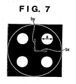
- Fig. 7 is a view showing an effective light source according to the first working example of the present invention.
- Fig. 8 is a view showing mask data according to the first working example of the present invention.
- Fig. 9 is a graph showing a coherent map according to the first working example of the present invention.
- Fig. 10 is a graph showing regions where the coherence is equal to or higher than a set value in the coherent map according to the first working example of the present invention.
- Fig. 11 is a graph showing the simulation result of imaging characteristics according to the first working example of the present invention.
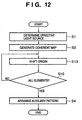
- Fig. 12 is a flowchart illustrating a processing sequence for generating mask data by executing a mask data generation program (second working example);
- Fig. 13 is a view showing pattern data according to the third working example of the present invention.
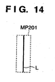
- Fig. 14 is a view showing another pattern data according to the third working example of the present invention.
- Fig. 15 is a graph showing an effective light source according to the third working example of the present invention.
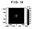
- Fig. 16 is a graph showing a coherent map according to the third working example of the present invention.
- Fig. 17 is a view showing mask data according to the third working example of the present invention.
- Fig. 18 is a graph showing an effective light source according to the fifth working example of the present invention.
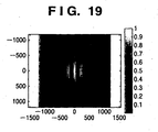
- Fig. 19 is a graph showing a coherent map according to the fifth working example of the present invention.
- Fig. 20 is a graph showing another coherent map according to the fifth working example of the present invention.
- Fig. 21 is a flowchart illustrating a processing sequence for generating mask data by executing a mask data generation program (sixth working example);
- Fig. 22 is a view showing pattern data according to the sixth working example of the present invention.
- Fig. 23 is a graph showing an effective light source according to the sixth working example of the present invention.
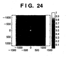
- Fig. 24 is a graph showing a coherent map according to the sixth working example of the present invention.
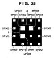
- Fig. 25 is a view showing mask data according to the sixth working example of the present invention.
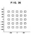
- Fig. 26 is a graph showing another pattern data according to the sixth working example of the present invention.
- Fig. 27 is a graph showing the initial value of the effective light source according to the sixth working example of the present invention.
- Fig. 28 is a schematic block diagram of an exposure apparatus
- Fig. 29 is a flowchart illustrating a device manufacturing method using an exposure apparatus.
- Fig. 30 is a flowchart illustrating the device manufacturing method using the exposure apparatus.
- the present invention is applicable especially in generating mask data used for micromechanics or various devices, e.g., a semiconductor chip such as an IC or LSI, a display element such as a liquid crystal panel, a detection element such as a magnetic head, and an image sensing element such as a CCD.
- the micromechanics here means a sophisticated micron-order machinery system or a technique of building this system, which are attained by applying a semiconductor integrated circuit manufacturing technology to the manufacture of a microstructure.
- the present invention is suitable for so-called immersion exposure for bringing the final surface of a projection optical system and the surface of a wafer into contact with a liquid, and forming a latent image on a photoresist via the projection optical system and liquid.
- the present invention discloses a concept which can be mathematically modeled. It is therefore possible to implement this concept as a software function of a computer system.
- the software function of the computer system includes programming executable software codes and enables an auxiliary pattern to be inserted in a mask pattern.
- a general computer can execute the software codes.
- the software codes or their associated data are stored in a general computer platform.
- the software is stored in another site or loaded by another appropriate general computer system.
- at least one machine-readable recording medium can hold the software codes as one or a plurality of modules.
- the invention to be described hereinafter is written in the code form as described above and can function as one or a plurality of software products.
- a processor of the computer system executes the software codes.
- the computer platform can execute methods to be described in this specification and shown in the embodiments, a catalog, or a software download function.
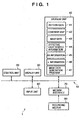
- a computer 1 comprises a bus 10, control unit 20, display unit 30, storage unit 40, input unit 60, and medium interface 70.
- the control unit 20, display unit 30, storage unit 40, input unit 60, and medium interface 70 connect to each other via the bus 10.
- the medium interface 70 is connectable to a recording medium 80.
- the storage unit 40 stores pattern data 41, coherent map 42, mask data 43, effective light source information 44, NA information 45, ⁇ information 46, and mask data generation program 47 which generates mask data.
- the pattern data 41 is of a pattern (to be referred to as a layout pattern hereinafter) having the layout design of, e.g., an integrated circuit.
- the coherent map 42 expresses a coherence distribution on a plane (the object plane of a projection optical system) on which a mask is arranged.
- the mask data 43 is used to draw a pattern of, e.g., Cr on the mask.
- the effective light source information 44 is associated with a light intensity distribution formed on a pupil plane 142 (see Fig.
- the NA information 45 is associated with an image side numerical aperture NA of the projection optical system in the exposure apparatus 100.
- the ⁇ information 46 is associated with the wavelength ⁇ of exposure light.
- the mask data generation program 47 is used to generate mask data.
- the control unit 20 is, e.g., a CPU, GPU, DSP, or microcomputer and further includes a cash memory for temporal storage.
- Examples of the display unit 30 are a CRT display and liquid crystal display.
- Examples of the storage unit 40 are a memory and hard disk.
- Examples of the input unit 60 are a keyboard and mouse.
- Examples of the medium interface 70 are a floppy(Japanese registered trademark) disk drive, CD-ROM drive, and USB interface.
- Examples of the recording medium 80 are a floppy disk, CD-ROM, and USB memory.
- ⁇ be the wavelength of exposure light of the exposure apparatus 100 (see Fig. 28 ), NA be the image side numerical aperture of the projection optical system, and ⁇ be the ratio between the object side numerical aperture of the projection optical system and a numerical aperture formed by the light beam guided to the mask surface by the illumination optical system.
- the exposure apparatus can take various NA and ⁇ values, it is convenient to normalize the pattern size by ( ⁇ /NA). For example, if ⁇ is 248 nm and NA is 0.73, 100 nm is normalized into 0.29 in the above-described manner. This normalization will be called "conversion by a k1 value" throughout this specification.
- the size here means not the area but the length of one side of a pattern.
- a pattern (to be referred to as a mask pattern hereinafter) of, e.g., Cr drawn on the mask has a size different from that of a pattern (to be referred to as a wafer pattern hereinafter) formed on the wafer surface by the magnification of the projection optical system.
- a dimension (coordinate position) on the mask surface is indicated by a magnitude corresponding to the size of the wafer pattern obtained by multiplying the size of the mask pattern by the magnification of the projection optical system such that the sizes of the mask pattern and wafer pattern have a one-to-one correspondence.
- the mask surface here means the object plane of the projection optical system, on which the mask is arranged.
- a mask pattern and wafer pattern in the semiconductor exposure apparatus have a partial coherent imaging relationship.
- the partial coherent imaging requires effective light source information 44 to determine coherence on the mask surface.
- the coherence here means the degree of interference corresponding to distance on the mask surface. For example, when two elements of the mask pattern are arranged at a distance at which the coherence is 0, light beams diffracted by the two elements never interfere with each other.
- the coherence can be obtained by Fourier-transforming an effective light source in accordance with the van Cittert-Zernike theorem. More strictly speaking, the coherence is given as the absolute value of the Fourier transform of the effective light source. In the following description, the absolute value of the Fourier transform of the effective light source will be called a coherent map for convenience.
- the coherent map 42 expresses a coherence distribution on the mask surface, and always takes positive values.
- the interference map explained in "BACKGROUND OF THE INVENTION" expresses an approximate distribution of imaging plane amplitude, and takes positive or negative values. For this reason, the coherent map 42 and interference map deal with completely different physical quantities and have completely different properties.
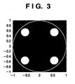
- Fig. 3 exemplifies the effective light source (effective light source information 44).
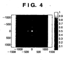
- Fig. 4 exemplifies the coherent map 42.
- Fig. 3 shows a light intensity distribution formed on the pupil plane of the projection optical system by the illumination optical system without a mask.
- the light intensity distribution is normalized assuming that the radius of the pupil of the projection optical system is 1.
- the NA (the image side numerical aperture of the projection optical system) of the exposure apparatus is 0.73, and the wavelength is 248 nm.
- Fig. 4 shows the coherent map 42 obtained by Fourier-transforming a function indicating the effective light source shown in Fig. 3 .
- the abscissa indicates the x coordinate of the mask surface (unit: nm)
- the ordinate indicates the y coordinate of the mask surface (unit: nm).
- Fig. 4 expresses coherence on the mask surface with respect to the origin (0 nm, 0 nm).
- the mask data 43 generated using the coherent map 42 will be explained.
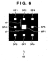
- Fig. 5 shows a binary mask (a black portion indicates the light-shielding portion, and a white portion indicates the transmission portion). The length of one side of the opening portion is 120 nm.
- a pattern of, e.g., Cr is drawn on the mask directly using the pattern data 41 (layout pattern data) shown in Fig. 5 as the mask data 43.
- the pattern data 41 layout pattern data
- a light intensity distribution gradually changes. Consequently, accurate micropattern formation may not be possible.
- a contact hole pattern as an element of the processing target pattern data 41 (layout pattern data) shown in Fig. 5 is selected as an element of interest.
- the origin of the coherent map 42 shown in Fig. 4 is matched with the contact hole of the pattern data 41 shown in Fig. 5 so that the contact hole pattern serves as the main pattern.
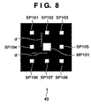
- auxiliary patterns are laid out near regions (+310 nm, 0nm), (0 nm, ⁇ 310 nm), and ( ⁇ 310 nm, ⁇ 310 nm) where the coherence is equal to or higher than a set value (e.g., 0.7). That is, as shown in Fig.
- auxiliary patterns SP1 to SP8 are laid out around a main pattern MP1 that is the contact hole pattern in Fig. 5 .
- a pattern of, e.g., Cr is drawn on the mask using the data shown in Fig. 6 as the mask data 43 (mask fabrication). In exposure, light diffracted by the mask pattern (including the main pattern and auxiliary patterns) forms an image on the photoresist on the wafer surface while maintaining high coherence. Consequently, the imaged light intensity distribution drastically changes. This allows accurate micropattern formation.
- the size of the auxiliary pattern of the mask data 43 as shown in Fig. 6 is small enough not to resolve and is desirably 75% that of the main pattern (contact hole pattern) or its neighborhood.
- the size here means not the area but the length of one side of a pattern.
- the auxiliary patterns are added to high-coherence regions. For this reason, arranging the auxiliary patterns considerably improves the resolution.
- the size of the auxiliary pattern is not limited to 75% that of the main pattern (contact hole pattern) or its neighborhood. Examinations made by the inventors of the present invention have revealed that a sufficient effect can be produced even when the size of the auxiliary pattern is 50% to 85% that of the main pattern (contact hole pattern). That is, even in this case, the auxiliary patterns allow the main pattern to accurately form an image on the wafer surface without being resolved.
- auxiliary pattern may be a rectangular pattern having sides with a length of 50% to 85% and those with a length of 50% to 85%.
- the main pattern contact hole pattern
- the auxiliary pattern has a longer side with a dimension of A ⁇ 50% to 85% and a shorter side with a dimension of B ⁇ 50% to 85%.
- auxiliary line patterns Assume, for example, that the main pattern (line pattern) has a length C and a width D ( ⁇ C). Since the line pattern is resolved more readily than the contact hole pattern, the auxiliary pattern preferably has a width of D ⁇ 35% to 70% and a length almost equal to C.
- the shape of the auxiliary pattern of the mask data 43 is almost similar to that of the main pattern.
- the main pattern e.g., a contact hole pattern
- roughly square auxiliary patterns are preferably added to the mask data 43.
- the main pattern contact hole pattern
- rectangular auxiliary patterns are preferably added to the mask data 43. How to determine another auxiliary pattern shape will be clarified in the embodiments to be described later.
- step S1 the control unit 20 of the computer 1 determines an effective light source.
- the user inputs information associated with an effective light source (shown in, e.g., Fig. 3 ) to the input unit 60 in advance.
- the control unit 20 Upon receiving the information associated with the effective light source, the control unit 20 stores it in the storage unit 40 as the effective light source information 44.
- the pattern data 41, NA information 45, and ⁇ information 46 are also input to the input unit 60 in advance by the user, and stored in the storage unit 40 via the control unit 20.
- the recording medium 80 which records the mask data generation program 47 connects to the medium interface 70.
- the mask data generation program 47 is installed and stored in the storage unit 40 via the control unit 20.
- the user inputs an instruction to start up the mask data generation program 47 to the input unit 60.
- the control unit 20 refers to the storage unit 40 and starts up the mask data generation program 47 on the basis of this instruction.
- the control unit 20 then controls the display unit 30 to display effective light source information 44 in accordance with the mask data generation program 47.
- the user having browsed the effective light source information 44 inputs an instruction to select the effective light source to the input unit 60.
- the control unit 20 determines the effective light source intensity distribution (see Fig. 3 ) and holds the determined effective light source information.
- step S2 the control unit 20 of the computer 1 generates a coherent map 42.
- the control unit 20 Upon receiving the instruction to generate a coherent map 42, the control unit 20 refers to the storage unit 40 and receives the NA information 45 and ⁇ information 46 on the basis of this instruction. On the basis of the effective light source information, the control unit 20 generates a function indicating the effective light source. On the basis of the NA information 45 and ⁇ information 46, the control unit 20 Fourier-transforms the function indicating the effective light source to generate coherent map 42 (see Fig. 4 ). The control unit 20 then controls the display unit 30 to display the coherent map 42.
- step S3 the control unit 20 of the computer 1 shifts the origin of the coherent map 42.
- the control unit 20 Upon receiving the instruction to display the pattern data 41, the control unit 20 refers to the storage unit 40 and controls the display unit 30 to display the pattern data 41, on the basis of this instruction. With this operation, the display unit 30 simultaneously displays the pattern data 41 and coherent map 42.
- the user having browsed the pattern data 41 and coherent map 42 inputs an instruction to select an element of interest (of the pattern data 41) to the input unit 60.
- the control unit 20 shifts the origin of the coherent map 42 to the center of the element of interest of the pattern data 41 and matches them on the basis of this instruction.
- the control unit 20 then controls the display unit 30 to display the pattern data 41 and the coherent map 42 with the origin being shifted.
- the control unit 20 generates mask data 43 using the element of interest as the main pattern, and stores it in the storage unit 40.
- step S4 the control unit 20 of the computer 1 arranges an auxiliary pattern.
- the control unit 20 Upon receiving the instruction to arrange the auxiliary pattern, the control unit 20 additionally arranges the auxiliary pattern in a region where the coherence is equal to or higher than a set value, on the basis of this instruction.
- the control unit 20 refers to the storage unit 40 and sets the mask data 43 including the auxiliary pattern information as new mask data 43.
- the control unit 20 then controls the display unit 30 to display the mask data 43 in place of the pattern data 41.
- the control unit 20 stores the mask data 43 in the storage unit 40.
- the process by the mask data generation program 47 can generate, using the coherent map 42, mask data 43 in which auxiliary patterns are arranged at appropriate positions. That is, the process by the mask data generation program 47 can generate mask data 43 in which auxiliary patterns are arranged at appropriate positions without calculating either the TCC or eigenfunction, thus simplifying the whole numerical calculation. This makes it possible to shorten the generation time of the mask data 43.
- an EB drawing apparatus When an EB drawing apparatus receives the mask data 43, it can draw a pattern of, e.g., Cr corresponding to the mask data 43 on a mask 130. This makes it possible to fabricate the mask 130.
- the mask data may include other patterns except the patterns generated using the coherent map, and that the mask being drawn the patterns including other patterns may be fabricated.
- FIG. 5 Consider pattern data having an isolated (minute) square contact hole shown in Fig. 5 as an example of pattern data 41.
- the NA of an exposure apparatus 100 (see Fig. 28 ) is 0.73, and the wavelength ⁇ of exposure light is 248 nm.
- the size of the contact hole is 120 nm.
- An effective light source has an appearance as shown in Fig. 7 .
- White portions indicate light irradiated portions, which are called poles in this specification.
- a diameter a of each pole is 0.2 when converting the diameter into a ⁇ value.
- a value obtained upon conversion into the ⁇ value indicates a magnitude obtained by normalization assuming that the radius of the pupil of a projection optical system is 1.
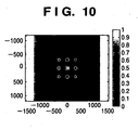
- a control unit 20 generates a coherent map 42 as shown in Fig. 9 .
- the scale of Fig. 9 is identical to that shown in Fig. 4 .
- the control unit 20 determines the coherence threshold value (set value).
- the control unit 20 determines the coherence set value as 0.5.
- Fig. 10 shows regions where the coherence exceeds 0.5 (set value) in the coherent map 42.
- Positions where the coherence exceeds the threshold value (set value) and corresponds to a peak are ( ⁇ 310 nm, 0 nm), (0 nm, ⁇ 310 nm), and ( ⁇ 310 nm, ⁇ 310 nm) on the mask.
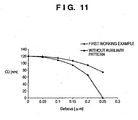
- the simulation result of the imaging characteristic of a mask without any auxiliary patterns is compared with that of a mask fabricated by the auxiliary pattern insertion method according to this working example.
- Fig. 11 shows the simulation result of imaging characteristics.
- the abscissa indicates the defocus amount
- the ordinate indicates the hole diameter (CD; Critical Dimension).
- the imaging performance of a mask without any auxiliary patterns is compared with that of a mask fabricated by the mask data generation method according to this working example. This reveals that the mask fabricated by the mask data generation method according to this working example dramatically decreases a change in hole diameter as a function of the defocus. That is, this working example is advantageous to accurate micropattern formation owing to an improvement in imaging characteristic.
- the coherent map 42 is calculated and the auxiliary patterns are arranged at positions where the coherence exceeds the threshold value (set value) and corresponds to a peak, thus improving the imaging characteristic. This allows accurate micropattern formation.
- the first working example has exemplified the case wherein the pattern data 41 includes one element.
- the second working example will exemplify a case wherein pattern data 41 includes a plurality of elements.
- n (n is a natural number equal to or larger than 2) contact hole patterns scattered on the pattern data 41.
- a coherent map 42 is an estimate of the degree of interference with the origin. That is, the coherent map 42 expresses the coherence between a certain point and the origin. As described in the first working example, the use of the coherent map 42 allows an improvement in imaging performance.
- a processing sequence for generating mask data by executing a mask data generation program shown in Fig. 12 is different from that shown in Fig. 2 in the following points.
- Fig. 12 is a flowchart illustrating a processing sequence for generating mask data by executing a mask data generation program.
- step S13 the user having browsed the pattern data 41 and coherent map 42 inputs an instruction to select an element of interest from unselected contact holes of the n contact holes to an input unit 60.
- a control unit 20 adds the coherent map 42 with the origin being shifted to the center of the element of interest to a synthetic coherent map 42i (i is a natural number) to generate a new synthetic coherent map 42i+1.
- the synthetic coherent map 42i is obtained by overlapping coherent maps 42 for i elements of interest. Other points are the same as those in step S3 shown in Fig. 2 .
- step S15 the control unit 20 determines whether all the elements of the pattern data 41, i.e., all of the n contact holes have been selected. If the control unit 20 determines that all of the n contact holes have been selected, the process advances to step S4. If the control unit 20 determines that not all of the n contact holes have been selected, the process returns to step S13.
- the first working example has exemplified the case wherein an element included in the pattern data 41 is a square pattern.
- the third working example will exemplify a case wherein an element included in pattern data 41 is a rectangular or line pattern.
- An element of interest selected by a control unit 20 is not limited to a square contact hole pattern.
- the element of interest may be, e.g., a rectangular contact hole pattern or line pattern.
- the element of interest is a rectangular contact hole pattern, it suffices to regard it as a line.
- the line passes through the center of the pattern in the shorter side direction and extends in the longer side direction.
- the length of the line is equal to the dimension of the mask pattern in the longer side direction.
- control unit 20 forms a line L as shown in Fig. 14 for a rectangular contact hole pattern MP201. Along the obtained line L, the control unit 20 adds coherent maps 42 to generate a synthetic coherent map 42L.
- the line L is described by a function 1 (x, y) .
- 1 (x, y) is 1 on the line but is 0 at positions other than the line.
- equation (2) a multiple integral is performed for the function 1(x,y) indicating the line L.
- the control unit 20 determines a dipole effective light source as shown in Fig. 15 .
- the control unit 20 On the basis of NA information 45 and ⁇ information 46, the control unit 20 Fourier-transforms a function indicating the effective light source shown in Fig. 15 to generate a coherent map 42 shown in Fig. 16 .
- the scale of Fig. 16 is identical to that shown in Fig. 4 .
- the coherent map 42 shown in Fig. 16 has parallel coherence peaks in the abscissa direction, i.e., x direction at a pitch of 213 nm.
- the control unit 20 matches the origin of the coherent map 42 shown in Fig. 16 with the position of an element (contact hole pattern MP201) of interest of the pattern data 41 shown in Fig. 13 .
- the control unit 20 arranges the main pattern MP 201 at the origin of mask data 43, and arranges auxiliary patterns SP201 to SP204 in regions where the coherence is equal to or higher than a set value.
- the coherent maps 42 defined by equations (1) and (2) are derived on the basis of points or lines. That is, in the above-described working examples, a square contact hole pattern is regarded as a set of points and a rectangular contact hole pattern or line pattern is regarded as a set of lines to derive the coherent map 42. This method is effective when the size of a target contact hole is small or the width of a line is narrow.
- an actual contact hole has a finite size
- an actual line also has a finite width.
- a method of deriving a coherent map 42 (to be referred to as a finite-size coherent map hereinafter) will be explained by taking finite sizes into consideration.
- Rect(x/e,y/e) is a function which indicates a square contact hole pattern and takes 1 if
- control unit 20 When n square contact hole patterns exist, the control unit 20 performs an arithmetic process by replacing f (x, y) by F3 (x, y) in equation (1). This makes it possible to obtain a coherent map 42 indicated by F1 (x,y), i.e., an infinite-size coherent map 42 formed by the n square contact hole patterns.
- the control unit 20 may derive F3(x,y) indicating the finite-size coherent map 42 for a rectangular contact hole pattern. Let e1 be the length of a side of the rectangle in the x direction, and e2 be the length of a side in the y direction. Then, the control unit 20 derives F3(x,y) by replacing Rect(x/e,y/e) by Rect(x/el,y/e2). This makes it possible to obtain a finite-size coherent map 42 for the rectangular contact hole pattern.
- control unit 20 When n rectangular contact hole patterns exist, the control unit 20 performs an arithmetic process by replacing f(x,y) by F3(x,y) in equation (1). This makes it possible to obtain a coherent map 42 indicated by F1(x,y), i.e., a infinite-size coherent map 42 formed by the n rectangular contact hole patterns.
- the control unit 20 may calculate the finite-size coherent map 42 by regarding a rectangular contact hole pattern as a set of square contact hole patterns. That is, the control unit 20 replaces Rect(x/e,y/e) by Rect(x/el,y/el) in equation (3) if e1 is smaller than e2.
- the control unit 20 calculates F4(x,y) indicating the finite-size coherent map 42 for the square contact hole pattern.
- the control unit 20 prepares a line which passes through the center of the pattern in the shorter side direction, extends in the longer side direction, and has a length e2.
- the control unit 20 calculates F2(x,y) indicating the finite-size coherent map 42 for the rectangular contact hole pattern by replacing f(x,y) by F4(x,y) using 1(x,y) as a function indicating the line with the length e2 in equation (2).
- control unit 20 may calculate the finite-size coherent map 42 by regarding a line pattern as a set of square contact hole patterns.
- control unit 20 may multiply a function indicating a side of a layout pattern by the function indicating the coherent map 42 and integrate the product to derive the finite-size coherent map 42 which can enhance the side of the mask pattern.
- auxiliary patterns are arranged using a coherent map corresponding to even a finite-size element. This makes it possible to accurately form a micropattern on a wafer.
- a control unit 20 derives the van Cittert-Zernike theorem by applying the NA of a projection optical system to the ⁇ value of an effective light source, and three-dimensionally expressing polarized light to be condensed. That is, the control unit 20 performs Fourier transformation by multiplying a function indicating an effective light source by a factor associated with polarization.
- Polarization factors include a factor which allows x-polarized light to remain as x-polarized, one which turns x-polarized light into y-polarized light, one which turns x-polarized light into z-polarized light, one which turns y-polarized light into x-polarized light, one which allows y-polarized light to remain as y-polarized, and one which turns y-polarized light into z-polarized light.
- the function obtained by multiplying the function indicating the effective light source by a polarization factor maintains the characteristics of the effective light source.
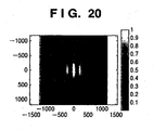
- a coherent map 42 which incorporates the polarization effect will be exemplified.
- control unit 20 performs Fourier transformation by multiplying a function indicating an effective light source by a y-polarized light (S-polarized light) factor to generate a coherent map 42 shown in Fig. 19 .
- the scale of Fig. 19 is identical to that shown in Fig. 4 .
- control unit 20 performs Fourier transformation by multiplying a function indicating an effective light source by an x-polarized light (P-polarized light) factor to generate a coherent map 42 shown in Fig. 20 .
- the scale of Fig. 20 is identical to that shown in Fig. 19 .
- the polarization state also includes a non-polarized state (i.e., a state wherein polarization randomly changes). It is also possible to regard a coherent map 42 obtained by the conventional scalar approximation as a coherent map 42 which incorporates the polarization effect and does not contain polarized light.
- a coherent map is generated by taking the influence of polarization into consideration to arrange auxiliary patterns using this map. This makes it possible to accurately form a micropattern on a wafer.
- a control unit 20 may optimize an effective light source. That is, the control unit 20 determines an effective light source such that a peak (a region where the coherence is equal to or higher than a set value) of a coherent map 42 matches the position of an element of pattern data 41. With this operation, the effective light source becomes suitable for accurate micropattern formation.
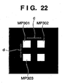
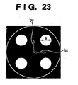
- Fig. 22 is a view showing pattern data according to the sixth working example of the present invention.
- White portions indicate light irradiated portions.
- a diameter a of each pole is 0.2 when converting the diameter into a ⁇ value.
- the control unit 20 Fourier-transforms a function indicating an effective light source, as shown in Fig. 23 , to generate a coherent map 42 on the mask surface with respect to the origin, as shown in Fig. 24 .
- the scale of Fig. 24 is identical to that shown in Fig. 4 .
- regions with high coherence appear at a pitch of 310 nm.
- the control unit 20 shifts the origin of the coherent map 42 to the position of one of elements MP301 to MP303 of interest of the pattern data 41 and matches them.
- the control unit 20 arranges auxiliary patterns at positions where the coherence in the coherence map 42 is equal to or higher than a set value and corresponds to a peak. As the control unit 20 performs this operation for all the elements MP301 to MP303 of interest and arranges auxiliary patterns SP301 to SP312, optimal mask data 43 as shown in Fig. 25 can be obtained.
- the use of the mask data 43 shown in Fig. 25 allows accurate micropattern formation.
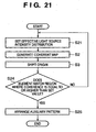
- a processing sequence for generating mask data by executing a mask data generation program shown in Fig. 21 is different from that shown in Fig. 2 in the following points.
- step S21 the control unit 20 sets an effective light source.
- the control unit 20 refers to a database (not shown) concerning a function indicating the effective light source and selects and sets this function.
- step S24 the control unit 20 determines whether a region where the coherence is equal to or higher than a set value matches the position of each of the main patterns MP301 to MP303. If YES in step S24, the control unit 20 arranges each of the auxiliary patterns SP301 to SP312 at a position where the coherence is equal to or higher than the set value and matches none of the main patterns MP301 to MP303. The control unit 20 then generates mask data 43. For example, the control unit 20 generates mask data 43 shown in Fig. 25 .
- step S24 the process returns to step S21 to set an effective light source again.
- Light diffracted by the mask pattern forms a diffracted light distribution on the pupil plane of a projection optical system.
- O(fx,fy) be the diffracted light distribution.
- the coordinate position (fx,fy) on the pupil plane is normalized so that the pupil radius is 1.
- Let circ(fx-a,fy-b) be a function which takes 1 when it falls within a circle having a radius of 1 from the center (a,b), and otherwise, takes 0.
- Let w(fx,fy) be the weighting function of the diffracted light.
- Fig. 26 is a graph showing another pattern data according to the sixth working example of the present invention.
- the ordinate indicates the y-coordinate (unit: nm) of the mask surface
- the abscissa indicates the x-coordinate (unit: nm) of the mask surface.
- the NA of the exposure apparatus 100 (see Fig. 28 ) is 0.73, and the wavelength of exposure light is 248 nm.
- the control unit 20 calculates the function S(fx,fy) indicating an effective light source.
- Fig. 27 shows the effective light source indicated by the function S(fx,fy) calculated by the control unit 20.
- the weighting function w(fx,fy) is roughly a quadratic function.
- the abscissa and ordinate have scales in which coordinates are normalized using the radius of the pupil of the projection optical system as 1, and the color density indicates the magnitude of the light intensity.
- the light intensity changes continuously.
- the effective light source shown in Fig. 27 is similar to that shown in Fig. 23 . That is, the distribution shown in Fig. 27 is suitable as the initial value (the set value of the effective light source) set in step S21 of the loop from step S21 to step S24 to optimize the effective light source.
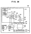
- Fig. 28 is a schematic block diagram of the exposure apparatus 100.
- the exposure apparatus 100 comprises an illumination unit 110, mask stage 132, projection optical system 140, main control unit 150, monitor and input unit 152, and wafer stage 176.
- a mask 130 is any one of those fabricated in the first to sixth working examples.
- the exposure apparatus 100 is an immersion exposure apparatus which transfers the mask pattern onto a wafer 174 by exposure via a liquid 180 while the wafer 174 and the final surface of the projection optical system 140 are in contact with the liquid 180.
- the exposure apparatus 100 is a step-and-scan projection exposure apparatus, it may adopt the step-and-repeat scheme or another exposure scheme.
- the illumination unit 110 illuminates the mask 130 on which the circuit pattern to be transferred is formed, and comprises a light source unit and illumination optical system.
- the illumination unit 110 forms the effective light source as described in the above working examples on the pupil plane of the projection optical system.
- the light source unit includes a laser 112 serving as a light source, and a beam shaping system 114.
- the laser 112 uses a KrF excimer laser having a wavelength of 248 nm.
- the laser 112 can adopt an ArF excimer laser having a wavelength of about 193 nm or an F 2 excimer laser having a wavelength of about 157 nm.
- the beam shaping system 114 shapes the section of collimated light from the laser 112 and guides the shaped light to an optical integrator 118 (to be described later).
- the illumination optical system illuminates the mask 130.
- the illumination optical system includes a condenser optical system 116, polarization control means 117, optical integrator 118, aperture stop 120, condenser lens 122, bending mirror 124, masking blade 126, and imaging lens 128.
- the illumination optical system can attain various illumination modes such as off axis illumination shown in Fig. 7 or 18 , in addition to normal illumination.
- the condenser optical system 116 includes a plurality of optical elements, and efficiently guides a light beam with a desired shape to the optical integrator 118.
- the condenser optical system 116 includes a zoom lens system and controls the allocation of the shape and angle of a beam that enters the optical integrator 118.
- the condenser optical system 116 includes an exposure amount adjusting unit which can change the amount of illumination light to expose the mask 130 for every illumination.
- the polarization control means 117 includes, e.g., a polarizing element and is nearly conjugate to a pupil plane 142 of the projection optical system 140. As described with reference to Fig. 7 , the polarization control means 117 controls the polarization state of a predetermined region of an effective light source formed on the pupil plane 142.
- a polarization control means 117 including a plurality of types of polarizing elements may be arranged on a turret which can be rotated by an actuator (not shown), and the main control unit 150 may control to drive the actuator.
- the optical integrator 118 is a member for making illumination light to be applied to the mask 130 uniform.
- the optical integrator 118 uses a fly-eye lens.
- the optical integrator 118 can use, e.g., an optical rod, diffraction optical element, or microlens array.
- the aperture stop 120 having a fixed shape and diameter is inserted immediately after the exit surface of the optical integrator 118.
- the aperture stop 120 is nearly conjugate to the pupil plane 142 of the projection optical system 140.
- the aperture shape of the aperture stop 120 corresponds to an effective light source as shown in Fig. 7 or 18 , which is formed on the pupil plane 142 of the projection optical system 140.
- the aperture stop 120 controls the effective light source.
- a diffractive optical element e.g. CGH
- a prism may be arranged in the light source side of the optical integrator 118, and that the effective light source may be shaped by using the diffractive optical element or the prism in lieu of using the aperture stop.
- a stop exchange mechanism (actuator) 121 can switch the aperture stop 120 to be inserted in the optical path, in accordance with the illumination condition.
- a driving control unit 151 controlled by the main control unit 150 controls to drive the actuator 121.
- the aperture stop 120 may be formed integrally with the polarization control means 117.
- the condenser lens 122 condenses a plurality of light beams that have emerged from a secondary source near the exit surface of the optical integrator 118 and are transmitted through the aperture stop 120.
- the condenser lens 122 guides the light beams to be reflected by the bending mirror 124, and uniformly Kohler-illuminates the surface of the masking blade 126 as the light irradiated surface.
- the masking blade 126 is a field stop which includes a plurality of movable light-shielding plates and has a rectangular aperture shape.
- the imaging lens 128 projects the aperture shape of the masking blade 126 onto the surface of the mask 130.
- the mask 130 has a transfer pattern and auxiliary pattern formed, and is supported and driven by the mask stage 132. Light diffracted by the mask 130 is projected onto the wafer 174 via the projection optical system 140. The mask 130 is arranged at a position optically conjugate to the wafer 174.
- the mask 130 can use any one of a binary mask, halftone mask, and phase shift mask.
- the projection optical system 140 projects the pattern formed on the mask 130 onto the wafer 174.
- the projection optical system 140 can use a dioptric system including only a plurality of lens elements or a catadioptric system including a plurality of lens elements and at least one concave mirror.
- the main control unit 150 controls to drive each unit and especially controls illumination on the basis of information input from an input section of the monitor and input unit 152, and information (e.g., information sent from the detection unit 151) from the illumination unit 110.
- the main control unit 150 controls to drive the aperture stop 120 via the driving mechanism 121.
- a monitor of the monitor and input unit 152 displays control information obtained by the main control unit 150 and other information.
- the main control unit 150 receives information of the effective light source as described in the above working example (for example, the information of the effective light source calculated in sixth working example) via the monitor and input unit 152 from user, and controls the aperture stop (alternatively the diffractive optical element or the prism) to form the effective light source.
- a photoresist 172 is applied to a wafer 174 of the substrate 170. It should be noted that the substrate 170 may be replaced with a liquid crystal substrate or another exposure target body.
- a wafer stage 176 supports the wafer 174.
- a material which has a good transmittance of the exposure light wavelength, prevents dirt from adhering on the projection optical system, and well matches the resist process is selected as the liquid 180.
- This embodiment uses pure water.
- a light beam emitted by the laser 112 is shaped by the beam shaping system 114, and then guided to the optical integrator 118 via the condenser optical system 116.
- the optical integrator 118 makes the illumination light uniform, and the aperture stop 120 sets the effective light source as shown in Fig. 7 or 18 .
- the resultant illumination light illuminates the mask 130 under an optimal illumination condition via the condenser lens 122, bending mirror 124, masking blade 126, and imaging lens 128.
- the projection optical system 140 reduces and projects the light beam having passed through the mask 130 onto the wafer 174 with a predetermined magnification.
- the substrate 170 and the final surface of the projection optical system 140 are in contact with a liquid 180 having a refractive index higher than that of air; the NA of the projection optical system 140 is relatively high and also the resolution is so high as to form a fine micropattern on the wafer 170.
- a high-contrast image is formed on the photoresist 172 under polarization control.
- FIG. 29 is a flowchart for explaining the manufacture of a device (a semiconductor chip such as an IC or LSI, an LCD, or a CCD). The manufacture of a semiconductor chip will be exemplified here.
- step 1 circuit design
- the circuit of a device is designed. More specifically, a design is made at schematic levels on the basis of the functional specification and then a layout design is made.
- the layout design the above-described layout pattern is designed using CAD software to generate pattern data 41.
- step 2 a mask suitable to form the designed circuit pattern is fabricated. More specifically, mask data 43 is generated by the method according to the present invention. An EB drawing apparatus then receives the mask data 43 and draws a pattern of, e.g., Cr corresponding to the mask data 43 on the mask 130. With this operation, the mask 130 is fabricated.
- step 3 wafer manufacture
- step 4 wafer process
- step 5 wafer process
- step 5 assembly
- step 6 semiconductor device manufactured in step 5 undergoes inspections such as an operation confirmation test and durability test. After these steps, the semiconductor device is completed and shipped in step 7 (shipment).
- Fig. 30 is a flowchart illustrating details of the wafer process in step 4.
- step 11 oxidation
- step 12 CVD
- step 13 electrode formation
- step 14 ion implantation
- ions are implanted in the wafer.
- step 15 resist process
- step 16 exposure
- step 18 exposure apparatus 100 transfers the circuit pattern of the mask onto the wafer by exposure.
- step 17 development
- step 18 etching
- steps other than the developed resist image are etched.
- step 19 resist removal
- This device manufacturing method can improve the yield in device manufacture.
- the halftone mask here means a mask in which a light-shielding portion of a binary mask is made of a translucent member and an opening portion exhibits a phase difference of 180°. Note that the use of a halftone mask requires a mask pattern larger than an exposure pattern.
Description
- The present invention relates to mask data generation program, mask data generation method, mask fabrication method, exposure method, and device manufacturing method.
- There has conventionally been used a projection exposure apparatus which causes a projection optical system to transfer the circuit pattern drawn on a mask (reticle) onto a substrate (e.g. a wafer). Under the circumstances, a demand for a high-resolution exposure apparatus is increasing. Known high-resolution exposure methods increase the numerical aperture (NA) of a projection optical system, shorten the exposure wavelength (λ), or decrease the k1 factor.
- Circuit patterns are roughly classified into interconnection patterns (line patterns) and contact hole patterns. Generally speaking, it is more difficult to expose fine contact hole patterns than fine line patterns.
- Various improvements in exposure techniques are being attempted to form fine contact hole patterns by exposure. A representative technique inserts an auxiliary pattern that is not resolvable in a mask on which a contact hole pattern to be transferred is drawn. This is one approach to decreasing the k1 factor.
-
Japanese Patent Laid-Open Nos. 2004-221594 2005-183981 - More specifically, a transmission cross coefficient (to be referred to as a TCC hereinafter) is derived. An aerial image undergoes decomposition (singular value decomposition; SVD) into N images (called eigenfunctions, N: Natural number) on the basis of the TCC result. This method is called sum of coherent system decomposition (to be referred to as SOCS hereinafter).
- The N eigenfunctions decomposited by SOCS each have a positive or negative value. An eigenvalue (ith eigenvalue) corresponding to the ith eigenfunction is multiplied by the square of the absolute value of the ith eigenfunction to obtain N functions. The N functions are added to obtain an aerial image.
- Assuming that a largest eigenvalue is the first eigenvalue and its corresponding eigenfunction is the first eigenfunction, the first eigenfunction most contributes to forming an aerial image. In view of this, the aerial image is approximated by the first eigenfunction. This approximation allows the derivation of an imaging plane amplitude distribution. That is, an interference map can be calculated.
- An auxiliary pattern is inserted in a portion having a positive value in the interference map such that exposure light transmitted through the contact hole pattern is in phase with that transmitted through the auxiliary pattern. An auxiliary pattern is inserted in a portion having a negative value in the interference map such that the phase difference between exposure light transmitted through the contact hole pattern and that transmitted through the auxiliary pattern is 180°.
- Unfortunately, the techniques described in
Japanese Patent Laid-Open Nos. 2004-221594 2005-183981 -
US 2005/0149900 A discloses a method for optimizing an intensity profile of a pattern to be formed in a surface of a substrate relative to a given mask using an optical system, wherein enhanced interference mapping lithography is used. - The present invention provides a mask data generation program and mask data generation method which can shorten the mask data generation time.
- The present invention provides the mask data generation method as claimed in
claim 1, the mask data generation program as claimed inclaim 5, the mask fabrication method as claimed inclaim 6, the exposure method as claimed inclaim 7, and the device manufacturing method as claimed in claim 9. The other claims relate to further developments. - According to the present invention, it is possible to shorten the mask data generation time.
- Further features of the present invention will become apparent from the following description of exemplary embodiments with reference to the attached drawings.
-
Fig. 1 is a block diagram showing the configuration of a computer according to an embodiment of the present invention; -
Fig. 2 is a flowchart illustrating a processing sequence for generating mask data by executing a mask data generation program (first working example); -
Fig. 3 is a graph showing an effective light source according to the embodiment of the present invention; -
Fig. 4 is a graph showing a coherent map according to the embodiment of the present invention; -
Fig. 5 is a view showing pattern data according to the embodiment of the present invention; -
Fig. 6 is a view showing mask data according to the embodiment of the present invention; -
Fig. 7 is a view showing an effective light source according to the first working example of the present invention; -
Fig. 8 is a view showing mask data according to the first working example of the present invention; -
Fig. 9 is a graph showing a coherent map according to the first working example of the present invention; -
Fig. 10 is a graph showing regions where the coherence is equal to or higher than a set value in the coherent map according to the first working example of the present invention; -
Fig. 11 is a graph showing the simulation result of imaging characteristics according to the first working example of the present invention; -
Fig. 12 is a flowchart illustrating a processing sequence for generating mask data by executing a mask data generation program (second working example); -
Fig. 13 is a view showing pattern data according to the third working example of the present invention; -
Fig. 14 is a view showing another pattern data according to the third working example of the present invention; -
Fig. 15 is a graph showing an effective light source according to the third working example of the present invention; -
Fig. 16 is a graph showing a coherent map according to the third working example of the present invention; -
Fig. 17 is a view showing mask data according to the third working example of the present invention; -
Fig. 18 is a graph showing an effective light source according to the fifth working example of the present invention; -
Fig. 19 is a graph showing a coherent map according to the fifth working example of the present invention; -
Fig. 20 is a graph showing another coherent map according to the fifth working example of the present invention; -
Fig. 21 is a flowchart illustrating a processing sequence for generating mask data by executing a mask data generation program (sixth working example); -
Fig. 22 is a view showing pattern data according to the sixth working example of the present invention; -
Fig. 23 is a graph showing an effective light source according to the sixth working example of the present invention; -
Fig. 24 is a graph showing a coherent map according to the sixth working example of the present invention; -
Fig. 25 is a view showing mask data according to the sixth working example of the present invention; -
Fig. 26 is a graph showing another pattern data according to the sixth working example of the present invention; -
Fig. 27 is a graph showing the initial value of the effective light source according to the sixth working example of the present invention; -
Fig. 28 is a schematic block diagram of an exposure apparatus; -
Fig. 29 is a flowchart illustrating a device manufacturing method using an exposure apparatus; and -
Fig. 30 is a flowchart illustrating the device manufacturing method using the exposure apparatus. - The present invention is applicable especially in generating mask data used for micromechanics or various devices, e.g., a semiconductor chip such as an IC or LSI, a display element such as a liquid crystal panel, a detection element such as a magnetic head, and an image sensing element such as a CCD. The micromechanics here means a sophisticated micron-order machinery system or a technique of building this system, which are attained by applying a semiconductor integrated circuit manufacturing technology to the manufacture of a microstructure. The present invention is suitable for so-called immersion exposure for bringing the final surface of a projection optical system and the surface of a wafer into contact with a liquid, and forming a latent image on a photoresist via the projection optical system and liquid.
- The present invention discloses a concept which can be mathematically modeled. It is therefore possible to implement this concept as a software function of a computer system. The software function of the computer system includes programming executable software codes and enables an auxiliary pattern to be inserted in a mask pattern. A general computer can execute the software codes. During operation of the software code, the software codes or their associated data are stored in a general computer platform. In some cases, the software is stored in another site or loaded by another appropriate general computer system. Accordingly, at least one machine-readable recording medium can hold the software codes as one or a plurality of modules. The invention to be described hereinafter is written in the code form as described above and can function as one or a plurality of software products. A processor of the computer system executes the software codes. The computer platform can execute methods to be described in this specification and shown in the embodiments, a catalog, or a software download function.
- The configuration of a computer for executing a mask data generation program according to an embodiment of the present invention will be explained next with reference to
Fig. 1 . - A
computer 1 comprises abus 10,control unit 20,display unit 30,storage unit 40,input unit 60, andmedium interface 70. - The
control unit 20,display unit 30,storage unit 40,input unit 60, andmedium interface 70 connect to each other via thebus 10. Themedium interface 70 is connectable to arecording medium 80. - The
storage unit 40stores pattern data 41,coherent map 42,mask data 43, effectivelight source information 44,NA information 45, λ information 46, and maskdata generation program 47 which generates mask data. Thepattern data 41 is of a pattern (to be referred to as a layout pattern hereinafter) having the layout design of, e.g., an integrated circuit. As will be described later, thecoherent map 42 expresses a coherence distribution on a plane (the object plane of a projection optical system) on which a mask is arranged. Themask data 43 is used to draw a pattern of, e.g., Cr on the mask. The effectivelight source information 44 is associated with a light intensity distribution formed on a pupil plane 142 (seeFig. 28 ) of the projection optical system in an exposure apparatus 100 (seeFig. 28 ; to be described later). TheNA information 45 is associated with an image side numerical aperture NA of the projection optical system in theexposure apparatus 100. The λ information 46 is associated with the wavelength λ of exposure light. The maskdata generation program 47 is used to generate mask data. - The
control unit 20 is, e.g., a CPU, GPU, DSP, or microcomputer and further includes a cash memory for temporal storage. Examples of thedisplay unit 30 are a CRT display and liquid crystal display. Examples of thestorage unit 40 are a memory and hard disk. Examples of theinput unit 60 are a keyboard and mouse. Examples of themedium interface 70 are a floppy(Japanese registered trademark) disk drive, CD-ROM drive, and USB interface. Examples of therecording medium 80 are a floppy disk, CD-ROM, and USB memory. - The arrangement of the
coherent map 42 according to the embodiment of the present invention will be explained. - Let λ be the wavelength of exposure light of the exposure apparatus 100 (see
Fig. 28 ), NA be the image side numerical aperture of the projection optical system, and σ be the ratio between the object side numerical aperture of the projection optical system and a numerical aperture formed by the light beam guided to the mask surface by the illumination optical system. - Since the exposure apparatus can take various NA and λ values, it is convenient to normalize the pattern size by (λ/NA). For example, if λ is 248 nm and NA is 0.73, 100 nm is normalized into 0.29 in the above-described manner. This normalization will be called "conversion by a k1 value" throughout this specification. The size here means not the area but the length of one side of a pattern.
- A pattern (to be referred to as a mask pattern hereinafter) of, e.g., Cr drawn on the mask has a size different from that of a pattern (to be referred to as a wafer pattern hereinafter) formed on the wafer surface by the magnification of the projection optical system. For the sake of simplicity, a dimension (coordinate position) on the mask surface is indicated by a magnitude corresponding to the size of the wafer pattern obtained by multiplying the size of the mask pattern by the magnification of the projection optical system such that the sizes of the mask pattern and wafer pattern have a one-to-one correspondence. The mask surface here means the object plane of the projection optical system, on which the mask is arranged.
- A mask pattern and wafer pattern in the semiconductor exposure apparatus have a partial coherent imaging relationship. The partial coherent imaging requires effective
light source information 44 to determine coherence on the mask surface. The coherence here means the degree of interference corresponding to distance on the mask surface. For example, when two elements of the mask pattern are arranged at a distance at which the coherence is 0, light beams diffracted by the two elements never interfere with each other. - The coherence can be obtained by Fourier-transforming an effective light source in accordance with the van Cittert-Zernike theorem. More strictly speaking, the coherence is given as the absolute value of the Fourier transform of the effective light source. In the following description, the absolute value of the Fourier transform of the effective light source will be called a coherent map for convenience.
- The
coherent map 42 expresses a coherence distribution on the mask surface, and always takes positive values. In contrast, the interference map explained in "BACKGROUND OF THE INVENTION" expresses an approximate distribution of imaging plane amplitude, and takes positive or negative values. For this reason, thecoherent map 42 and interference map deal with completely different physical quantities and have completely different properties. -
Fig. 3 exemplifies the effective light source (effective light source information 44).Fig. 4 exemplifies thecoherent map 42. -
Fig. 3 shows a light intensity distribution formed on the pupil plane of the projection optical system by the illumination optical system without a mask. Referring toFig. 3 , the light intensity distribution is normalized assuming that the radius of the pupil of the projection optical system is 1. White portions indicate light irradiated regions, and a circle which has a radius of 1 and is drawn by a white line indicates σ = 1. The NA (the image side numerical aperture of the projection optical system) of the exposure apparatus is 0.73, and the wavelength is 248 nm. -
Fig. 4 shows thecoherent map 42 obtained by Fourier-transforming a function indicating the effective light source shown inFig. 3 . Referring toFig. 4 , the abscissa indicates the x coordinate of the mask surface (unit: nm), and the ordinate indicates the y coordinate of the mask surface (unit: nm).Fig. 4 expresses coherence on the mask surface with respect to the origin (0 nm, 0 nm). - Referring to
Fig. 4 , as a value (color density value) when a highlight portion is becomes close to 1, the coherence with respect to the origin increases. As the color density value becomes close to 0, the coherence with respect to the origin decreases. For example, positions (±310 nm, 0 nm), (0 nm, ±310 nm), and (±310 nm, ±310 nm) on the mask surface exhibit high coherence with respect to the origin. - The
mask data 43 generated using thecoherent map 42 will be explained. - Consider pattern data having an isolated (minute) square contact hole shown in
Fig. 5 as an example of thepattern data 41. The NA of the exposure apparatus is 0.73, and the wavelength λ of exposure light is 248 nm. The size of the contact hole is 120 nm. To expose a contact hole, it is a common practice to use a mask pattern including a light-shielding portion and opening portion (transmission portion) as shown inFig. 5. Fig. 5 shows a binary mask (a black portion indicates the light-shielding portion, and a white portion indicates the transmission portion). The length of one side of the opening portion is 120 nm. - Assume that a pattern of, e.g., Cr is drawn on the mask directly using the pattern data 41 (layout pattern data) shown in
Fig. 5 as themask data 43. In exposure, light diffracted by the mask pattern forms an image on the photoresist on the wafer surface, and a light intensity distribution gradually changes. Consequently, accurate micropattern formation may not be possible. - To prevent this problem, according to this embodiment, a contact hole pattern as an element of the processing target pattern data 41 (layout pattern data) shown in
Fig. 5 is selected as an element of interest. The origin of thecoherent map 42 shown inFig. 4 is matched with the contact hole of thepattern data 41 shown inFig. 5 so that the contact hole pattern serves as the main pattern. Furthermore, auxiliary patterns are laid out near regions (+310 nm, 0nm), (0 nm, ±310 nm), and (±310 nm, ±310 nm) where the coherence is equal to or higher than a set value (e.g., 0.7). That is, as shown inFig. 6 , auxiliary patterns SP1 to SP8 are laid out around a main pattern MP1 that is the contact hole pattern inFig. 5 . The intervals between the main pattern MP1 and the auxiliary patterns SP2, SP4, SP5, and SP7 are d = 310 nm. The intervals d between the auxiliary patterns SP1, SP3, SP6, and SP8 and their adjacent auxiliary patterns SP2, SP5, SP4, and SP7 are d = 310 nm. A pattern of, e.g., Cr is drawn on the mask using the data shown inFig. 6 as the mask data 43 (mask fabrication). In exposure, light diffracted by the mask pattern (including the main pattern and auxiliary patterns) forms an image on the photoresist on the wafer surface while maintaining high coherence. Consequently, the imaged light intensity distribution drastically changes. This allows accurate micropattern formation. - Preferably, the size of the auxiliary pattern of the
mask data 43 as shown inFig. 6 is small enough not to resolve and is desirably 75% that of the main pattern (contact hole pattern) or its neighborhood. The size here means not the area but the length of one side of a pattern. An example of the size of the main pattern (contact hole pattern) is 120 nm inFig. 5 . That is, themask data 43 includes a 120-nm square pattern as the main pattern.
Accordingly, the size (the length of one side) of the auxiliary pattern is desirably 120 nm × 75% = 90 nm.
In this embodiment, however, the auxiliary patterns are added to high-coherence regions. For this reason, arranging the auxiliary patterns considerably improves the resolution. From this viewpoint, the size of the auxiliary pattern is not limited to 75% that of the main pattern (contact hole pattern) or its neighborhood. Examinations made by the inventors of the present invention have revealed that a sufficient effect can be produced even when the size of the auxiliary pattern is 50% to 85% that of the main pattern (contact hole pattern). That is, even in this case, the auxiliary patterns allow the main pattern to accurately form an image on the wafer surface without being resolved. - It should be noted that the auxiliary pattern may be a rectangular pattern having sides with a length of 50% to 85% and those with a length of 50% to 85%.
- Consider pattern data having an isolated (minute) rectangular contact hole as another example of the
pattern data 41. In this case, it suffices to additionally arrange rectangular auxiliary patterns. Assume, for example, that the main pattern (contact hole pattern) has a longer side with a dimension A and a shorter side with a dimension B (< A). Preferably, the auxiliary pattern has a longer side with a dimension of A × 50% to 85% and a shorter side with a dimension of B × 50% to 85%. - Consider isolated (fine) line pattern data as still another example of the
pattern data 41. In this case, it suffices to additionally arrange auxiliary line patterns. Assume, for example, that the main pattern (line pattern) has a length C and a width D (<< C). Since the line pattern is resolved more readily than the contact hole pattern, the auxiliary pattern preferably has a width of D × 35% to 70% and a length almost equal to C. - Preferably, the shape of the auxiliary pattern of the
mask data 43 is almost similar to that of the main pattern. For example, when the main pattern (e.g., a contact hole pattern) is a square, roughly square auxiliary patterns are preferably added to themask data 43. When the main pattern (contact hole pattern) is a rectangle, rectangular auxiliary patterns are preferably added to themask data 43. How to determine another auxiliary pattern shape will be clarified in the embodiments to be described later. - A processing sequence for generating mask data by executing a mask data generation program will be explained with reference to the flowchart shown in
Fig. 2 . - In step S1, the
control unit 20 of thecomputer 1 determines an effective light source. - That is, the user inputs information associated with an effective light source (shown in, e.g.,
Fig. 3 ) to theinput unit 60 in advance. Upon receiving the information associated with the effective light source, thecontrol unit 20 stores it in thestorage unit 40 as the effectivelight source information 44. Thepattern data 41,NA information 45, and λ information 46 are also input to theinput unit 60 in advance by the user, and stored in thestorage unit 40 via thecontrol unit 20. - The
recording medium 80 which records the maskdata generation program 47 connects to themedium interface 70. The maskdata generation program 47 is installed and stored in thestorage unit 40 via thecontrol unit 20. - The user inputs an instruction to start up the mask
data generation program 47 to theinput unit 60. Upon receiving the instruction to start up the maskdata generation program 47, thecontrol unit 20 refers to thestorage unit 40 and starts up the maskdata generation program 47 on the basis of this instruction. Thecontrol unit 20 then controls thedisplay unit 30 to display effectivelight source information 44 in accordance with the maskdata generation program 47. The user having browsed the effectivelight source information 44 inputs an instruction to select the effective light source to theinput unit 60. On the basis of the effectivelight source information 44 and the instruction to select the effective light source, thecontrol unit 20 determines the effective light source intensity distribution (seeFig. 3 ) and holds the determined effective light source information. - In step S2, the
control unit 20 of thecomputer 1 generates acoherent map 42. - That is, the user inputs an instruction to generate a
coherent map 42 to theinput unit 60. Upon receiving the instruction to generate acoherent map 42, thecontrol unit 20 refers to thestorage unit 40 and receives theNA information 45 and λ information 46 on the basis of this instruction. On the basis of the effective light source information, thecontrol unit 20 generates a function indicating the effective light source. On the basis of theNA information 45 and λ information 46, thecontrol unit 20 Fourier-transforms the function indicating the effective light source to generate coherent map 42 (seeFig. 4 ). Thecontrol unit 20 then controls thedisplay unit 30 to display thecoherent map 42. - In step S3, the
control unit 20 of thecomputer 1 shifts the origin of thecoherent map 42. - That is, the user inputs an instruction to display the
pattern data 41 to theinput unit 60. Upon receiving the instruction to display thepattern data 41, thecontrol unit 20 refers to thestorage unit 40 and controls thedisplay unit 30 to display thepattern data 41, on the basis of this instruction. With this operation, thedisplay unit 30 simultaneously displays thepattern data 41 andcoherent map 42. The user having browsed thepattern data 41 andcoherent map 42 inputs an instruction to select an element of interest (of the pattern data 41) to theinput unit 60. Upon receiving the instruction to select the element of interest, thecontrol unit 20 shifts the origin of thecoherent map 42 to the center of the element of interest of thepattern data 41 and matches them on the basis of this instruction. Thecontrol unit 20 then controls thedisplay unit 30 to display thepattern data 41 and thecoherent map 42 with the origin being shifted. In addition, thecontrol unit 20 generatesmask data 43 using the element of interest as the main pattern, and stores it in thestorage unit 40. - In step S4, the
control unit 20 of thecomputer 1 arranges an auxiliary pattern. - That is, the user having browsed the
pattern data 41 and thecoherent map 42 with the origin being shifted inputs an instruction to arrange an auxiliary pattern to theinput unit 60. Upon receiving the instruction to arrange the auxiliary pattern, thecontrol unit 20 additionally arranges the auxiliary pattern in a region where the coherence is equal to or higher than a set value, on the basis of this instruction. Thecontrol unit 20 refers to thestorage unit 40 and sets themask data 43 including the auxiliary pattern information asnew mask data 43. Thecontrol unit 20 then controls thedisplay unit 30 to display themask data 43 in place of thepattern data 41. In addition, thecontrol unit 20 stores themask data 43 in thestorage unit 40. - As described above, the process by the mask
data generation program 47 according to this embodiment can generate, using thecoherent map 42,mask data 43 in which auxiliary patterns are arranged at appropriate positions. That is, the process by the maskdata generation program 47 can generatemask data 43 in which auxiliary patterns are arranged at appropriate positions without calculating either the TCC or eigenfunction, thus simplifying the whole numerical calculation. This makes it possible to shorten the generation time of themask data 43. - When an EB drawing apparatus receives the
mask data 43, it can draw a pattern of, e.g., Cr corresponding to themask data 43 on amask 130. This makes it possible to fabricate themask 130. It should be noted that the mask data may include other patterns except the patterns generated using the coherent map, and that the mask being drawn the patterns including other patterns may be fabricated. - Working examples of the present invention will be explained below.
- Consider pattern data having an isolated (minute) square contact hole shown in
Fig. 5 as an example ofpattern data 41. The NA of an exposure apparatus 100 (seeFig. 28 ) is 0.73, and the wavelength λ of exposure light is 248 nm. The size of the contact hole is 120 nm. An effective light source has an appearance as shown inFig. 7 . A circle which has a radius of 1 and is drawn by a white line shown inFig. 7 indicates σ = 1. White portions indicate light irradiated portions, which are called poles in this specification. The distance from σ = 0 to the center of each pole is given such that the distance in the abscissa direction, i.e., x direction is bx = 0.55 (upon conversion into a σ value), and the distance in the ordinate direction, i.e., y direction is by = 0.55 (upon conversion into a σ value). A diameter a of each pole is 0.2 when converting the diameter into a σ value. A value obtained upon conversion into the σ value indicates a magnitude obtained by normalization assuming that the radius of the pupil of a projection optical system is 1. - First, a
control unit 20 generates acoherent map 42 as shown inFig. 9 . The scale ofFig. 9 is identical to that shown inFig. 4 . Next, thecontrol unit 20 determines the coherence threshold value (set value). For example, thecontrol unit 20 determines the coherence set value as 0.5.Fig. 10 shows regions where the coherence exceeds 0.5 (set value) in thecoherent map 42. Positions where the coherence exceeds the threshold value (set value) and corresponds to a peak are (±310 nm, 0 nm), (0 nm, ±310 nm), and (±310 nm, ±310 nm) on the mask. In view of this, thecontrol unit 20 arranges a main pattern MP101 at the origin ofmask data 43 shown inFig. 8 , and arranges auxiliary patterns SP101 to SP108 at an interval d = 310 nm. - The simulation result of the imaging characteristic of a mask without any auxiliary patterns is compared with that of a mask fabricated by the auxiliary pattern insertion method according to this working example.
-
Fig. 11 shows the simulation result of imaging characteristics. Referring toFig. 11 , the abscissa indicates the defocus amount, and the ordinate indicates the hole diameter (CD; Critical Dimension). The imaging performance of a mask without any auxiliary patterns is compared with that of a mask fabricated by the mask data generation method according to this working example. This reveals that the mask fabricated by the mask data generation method according to this working example dramatically decreases a change in hole diameter as a function of the defocus. That is, this working example is advantageous to accurate micropattern formation owing to an improvement in imaging characteristic. - According to this working example, the
coherent map 42 is calculated and the auxiliary patterns are arranged at positions where the coherence exceeds the threshold value (set value) and corresponds to a peak, thus improving the imaging characteristic. This allows accurate micropattern formation. - The first working example has exemplified the case wherein the
pattern data 41 includes one element. However, the second working example will exemplify a case whereinpattern data 41 includes a plurality of elements. - Consider, for example, n (n is a natural number equal to or larger than 2) contact hole patterns scattered on the
pattern data 41. - A
coherent map 42 is an estimate of the degree of interference with the origin. That is, thecoherent map 42 expresses the coherence between a certain point and the origin. As described in the first working example, the use of thecoherent map 42 allows an improvement in imaging performance. - When n contact hole patterns exist, they are individually processed as elements of interest. That is, a processing sequence for generating mask data by executing a mask data generation program shown in
Fig. 12 is different from that shown inFig. 2 in the following points.Fig. 12 is a flowchart illustrating a processing sequence for generating mask data by executing a mask data generation program. - In step S13, the user having browsed the
pattern data 41 andcoherent map 42 inputs an instruction to select an element of interest from unselected contact holes of the n contact holes to aninput unit 60. Acontrol unit 20 adds thecoherent map 42 with the origin being shifted to the center of the element of interest to a synthetic coherent map 42i (i is a natural number) to generate a new synthetic coherent map 42i+1. The synthetic coherent map 42i is obtained by overlappingcoherent maps 42 for i elements of interest. Other points are the same as those in step S3 shown inFig. 2 . - In step S15, the
control unit 20 determines whether all the elements of thepattern data 41, i.e., all of the n contact holes have been selected. If thecontrol unit 20 determines that all of the n contact holes have been selected, the process advances to step S4. If thecontrol unit 20 determines that not all of the n contact holes have been selected, the process returns to step S13. - The process shown in
Fig. 12 is formulated by equation (1). That is, letting f(x,y) be thecoherent map 42, and (xi,yi) be the coordinate position of the center position of an ith contact hole pattern, it suffices to determine, as a synthetic coherent map 42n, F1 (x, y) given by:
where i = 1 to n. Then, as described in the first working example, it suffices to arrange auxiliary patterns at positions where F1 (x,y) exceeds a predetermined threshold value and corresponds to a peak, thus improving the imaging characteristic. - In this manner, synthetic coherent maps corresponding to a plurality of elements are generated to arrange auxiliary patterns using these maps. This makes it possible to accurately form a micropattern including a plurality of elements.
- The first working example has exemplified the case wherein an element included in the
pattern data 41 is a square pattern. However, the third working example will exemplify a case wherein an element included inpattern data 41 is a rectangular or line pattern. - A method of arranging an auxiliary pattern by regarding a rectangular or linear pattern as a set of square patterns will be explained first.
- An element of interest selected by a
control unit 20 is not limited to a square contact hole pattern. The element of interest may be, e.g., a rectangular contact hole pattern or line pattern. - If, for example, the element of interest is a rectangular contact hole pattern, it suffices to regard it as a line. Note that the line passes through the center of the pattern in the shorter side direction and extends in the longer side direction. The length of the line is equal to the dimension of the mask pattern in the longer side direction.
- For example, the
control unit 20 forms a line L as shown inFig. 14 for a rectangular contact hole pattern MP201. Along the obtained line L, thecontrol unit 20 addscoherent maps 42 to generate a synthetic coherent map 42L. - That is, the line L is described by a function 1 (x, y) . Note that 1 (x, y) is 1 on the line but is 0 at positions other than the line. The synthetic coherent map 42L is given by:

where f(x,y) is thecoherent map 42. In equation (2), a multiple integral is performed for the function 1(x,y) indicating the line L. - Then, as described in the first working example, it suffices to insert auxiliary patterns in positions where F2(x,y) exceeds a predetermined threshold value and corresponds to a peak, thus improving the imaging characteristic.
- A method of arranging an auxiliary pattern on the basis of an effective light source suitable for a rectangular or linear pattern will be explained next.
- Assume, for example, that the NA of an exposure apparatus 100 (see
Fig. 28 ) is 0.73, and the wavelength λ of exposure light is 248 nm. The shorter side of the contact hole is 110 nm. Thecontrol unit 20 determines a dipole effective light source as shown inFig. 15 . White portions indicate light irradiated regions, and a circle which has a radius of 1 and is drawn by a white line indicates σ = 1. The distance from σ = 0 to the center of each pole in the abscissa direction is 0.8 when converting the distance into a σ value, and the diameter of each pole is 0.3 when converting the diameter into a σ value. - On the basis of
NA information 45 and λ information 46, thecontrol unit 20 Fourier-transforms a function indicating the effective light source shown inFig. 15 to generate acoherent map 42 shown inFig. 16 . The scale ofFig. 16 is identical to that shown inFig. 4 . Thecoherent map 42 shown inFig. 16 has parallel coherence peaks in the abscissa direction, i.e., x direction at a pitch of 213 nm. - The
control unit 20 matches the origin of thecoherent map 42 shown inFig. 16 with the position of an element (contact hole pattern MP201) of interest of thepattern data 41 shown inFig. 13 . Thecontrol unit 20 arranges the main pattern MP 201 at the origin ofmask data 43, and arranges auxiliary patterns SP201 to SP204 in regions where the coherence is equal to or higher than a set value. Hence, as shown inFig. 17 , the auxiliary patterns SP201 to SP204 are arranged on the both sides of the main pattern MP201 in themask data 43 at a pitch d = 213 nm. - In this manner, a coherent map corresponding to a rectangular or line element is generated to arrange auxiliary patterns using the resultant coherent map. This makes it possible to accurately form a rectangular or linear micropattern.
- The coherent maps 42 defined by equations (1) and (2) are derived on the basis of points or lines. That is, in the above-described working examples, a square contact hole pattern is regarded as a set of points and a rectangular contact hole pattern or line pattern is regarded as a set of lines to derive the
coherent map 42. This method is effective when the size of a target contact hole is small or the width of a line is narrow. - However, an actual contact hole has a finite size, and an actual line also has a finite width. In view of this, a method of deriving a coherent map 42 (to be referred to as a finite-size coherent map hereinafter) will be explained by taking finite sizes into consideration.
- Consider a square contact hole pattern having sides with a length e. The square contact hole pattern can be expressed by Rect (x/e,y/e). Rect(x,y) is a function which indicates a square contact hole pattern and takes 1 if |x| ≤ 1/2 and |y| ≤ 1/2, and otherwise, takes 0.
- F3(x,y) indicating the finite-size
coherent map 42 for the square contact hole pattern is given by:
where f(x,y) is a function indicating thecoherent map 42. That is, acontrol unit 20 multiplies acoherent map 42 defined for points by a function indicating the square contact hole pattern and integrates the product to obtain a function F3(x,y) indicating the finite-sizecoherent map 42. - When n square contact hole patterns exist, the
control unit 20 performs an arithmetic process by replacing f (x, y) by F3 (x, y) in equation (1). This makes it possible to obtain acoherent map 42 indicated by F1 (x,y), i.e., an infinite-sizecoherent map 42 formed by the n square contact hole patterns. - The
control unit 20 may derive F3(x,y) indicating the finite-sizecoherent map 42 for a rectangular contact hole pattern. Let e1 be the length of a side of the rectangle in the x direction, and e2 be the length of a side in the y direction. Then, thecontrol unit 20 derives F3(x,y) by replacing Rect(x/e,y/e) by Rect(x/el,y/e2). This makes it possible to obtain a finite-sizecoherent map 42 for the rectangular contact hole pattern. - When n rectangular contact hole patterns exist, the
control unit 20 performs an arithmetic process by replacing f(x,y) by F3(x,y) in equation (1). This makes it possible to obtain acoherent map 42 indicated by F1(x,y), i.e., a infinite-sizecoherent map 42 formed by the n rectangular contact hole patterns. - The
control unit 20 may calculate the finite-sizecoherent map 42 by regarding a rectangular contact hole pattern as a set of square contact hole patterns. That is, thecontrol unit 20 replaces Rect(x/e,y/e) by Rect(x/el,y/el) in equation (3) if e1 is smaller than e2. Thecontrol unit 20 calculates F4(x,y) indicating the finite-sizecoherent map 42 for the square contact hole pattern. Thecontrol unit 20 prepares a line which passes through the center of the pattern in the shorter side direction, extends in the longer side direction, and has a length e2. Thecontrol unit 20 calculates F2(x,y) indicating the finite-sizecoherent map 42 for the rectangular contact hole pattern by replacing f(x,y) by F4(x,y) using 1(x,y) as a function indicating the line with the length e2 in equation (2). - Likewise, the
control unit 20 may calculate the finite-sizecoherent map 42 by regarding a line pattern as a set of square contact hole patterns. - As another form, the
control unit 20 may multiply a function indicating a side of a layout pattern by the function indicating thecoherent map 42 and integrate the product to derive the finite-sizecoherent map 42 which can enhance the side of the mask pattern. - In this manner, auxiliary patterns are arranged using a coherent map corresponding to even a finite-size element. This makes it possible to accurately form a micropattern on a wafer.
- The normal van Cittert-Zernike theorem does not take the influence of polarization into consideration. In recent years, however, the influence of polarization is becoming non-negligible in exposing a pattern whose factor k1 is small.
- In view of this, the inventors of the present invention propose a method of incorporating the polarization effect into the van Cittert-Zernike theorem. More specifically, a
control unit 20 derives the van Cittert-Zernike theorem by applying the NA of a projection optical system to the σ value of an effective light source, and three-dimensionally expressing polarized light to be condensed. That is, thecontrol unit 20 performs Fourier transformation by multiplying a function indicating an effective light source by a factor associated with polarization. Polarization factors include a factor which allows x-polarized light to remain as x-polarized, one which turns x-polarized light into y-polarized light, one which turns x-polarized light into z-polarized light, one which turns y-polarized light into x-polarized light, one which allows y-polarized light to remain as y-polarized, and one which turns y-polarized light into z-polarized light. The function obtained by multiplying the function indicating the effective light source by a polarization factor maintains the characteristics of the effective light source. - A
coherent map 42 which incorporates the polarization effect will be exemplified. - Consider a case wherein the NA of an exposure apparatus is 0.73, and the wavelength λ of exposure light is 248 nm. Assume a dipole effective light source as shown in
Fig. 18 . White portions indicate light irradiated regions, and a circle which has a radius of 1 and is drawn by a white line indicates σ = 1. The distance from σ = 0 to the center of each pole in the abscissa direction is 0.8 when converting the distance into a σ value, and the diameter of each pole is 0.3 when converting the diameter into a σ value. - For example, the
control unit 20 performs Fourier transformation by multiplying a function indicating an effective light source by a y-polarized light (S-polarized light) factor to generate acoherent map 42 shown inFig. 19 . The scale ofFig. 19 is identical to that shown inFig. 4 . For example, thecontrol unit 20 performs Fourier transformation by multiplying a function indicating an effective light source by an x-polarized light (P-polarized light) factor to generate acoherent map 42 shown inFig. 20 . The scale ofFig. 20 is identical to that shown inFig. 19 . A comparison between thecoherent map 42 shown inFig. 19 and that shown inFig. 20 reveals that regions with high coherence can be clearly distinguished from those with low coherence with y-polarized light but not with x-polarized light. With this phenomenon, arranging auxiliary patterns in regions with high y-polarized light allows accurate micropattern formation. On the other hand, it is ineffective to arrange auxiliary patterns for x-polarized light. - It should be noted that the polarization state also includes a non-polarized state (i.e., a state wherein polarization randomly changes). It is also possible to regard a
coherent map 42 obtained by the conventional scalar approximation as acoherent map 42 which incorporates the polarization effect and does not contain polarized light. - In this manner, according to this working example, a coherent map is generated by taking the influence of polarization into consideration to arrange auxiliary patterns using this map. This makes it possible to accurately form a micropattern on a wafer.
- A
control unit 20 may optimize an effective light source. That is, thecontrol unit 20 determines an effective light source such that a peak (a region where the coherence is equal to or higher than a set value) of acoherent map 42 matches the position of an element ofpattern data 41. With this operation, the effective light source becomes suitable for accurate micropattern formation. - Assume, for example, that the NA of an exposure apparatus 100 (see
Fig. 28 ) is 0.73, and the wavelength λ of exposure light is 248 nm. Consider a case wherein an optimal effective light source is calculated for a layout pattern (pattern data 41) with elements laid out at an interval d = 310 nm, as shown inFig. 22. Fig. 22 is a view showing pattern data according to the sixth working example of the present invention. A circle which has a radius of 1 and is drawn by a white line shown inFig. 23 indicates σ = 1. White portions indicate light irradiated portions. The distance from σ = 0 to the center of each pole is given such that the distance in the abscissa direction, i.e., x direction shown inFig. 23 is bx = 0.55 when converting the distance into a σ value, and the distance in the ordinate direction, i.e., y direction shown inFig. 23 is by = 0.55 when converting the distance into a σ value. A diameter a of each pole is 0.2 when converting the diameter into a σ value. - The
control unit 20 Fourier-transforms a function indicating an effective light source, as shown inFig. 23 , to generate acoherent map 42 on the mask surface with respect to the origin, as shown inFig. 24 . The scale ofFig. 24 is identical to that shown inFig. 4 . In thecoherent map 42 shown inFig. 24 , regions with high coherence appear at a pitch of 310 nm. Thecoherent map 42 shown inFig. 24 is obviously suitable for the mask pattern shown inFig. 22 because contact holes of the mask pattern shown inFig. 22 are adjacent to each other at an interval d = 310 nm. - The
control unit 20 shifts the origin of thecoherent map 42 to the position of one of elements MP301 to MP303 of interest of thepattern data 41 and matches them. Thecontrol unit 20 arranges auxiliary patterns at positions where the coherence in thecoherence map 42 is equal to or higher than a set value and corresponds to a peak. As thecontrol unit 20 performs this operation for all the elements MP301 to MP303 of interest and arranges auxiliary patterns SP301 to SP312,optimal mask data 43 as shown inFig. 25 can be obtained. The use of themask data 43 shown inFig. 25 allows accurate micropattern formation. - A processing sequence for generating mask data by executing a mask data generation program shown in
Fig. 21 is different from that shown inFig. 2 in the following points. - In step S21, the
control unit 20 sets an effective light source. Thecontrol unit 20 refers to a database (not shown) concerning a function indicating the effective light source and selects and sets this function. - In step S24, the
control unit 20 determines whether a region where the coherence is equal to or higher than a set value matches the position of each of the main patterns MP301 to MP303. If YES in step S24, thecontrol unit 20 arranges each of the auxiliary patterns SP301 to SP312 at a position where the coherence is equal to or higher than the set value and matches none of the main patterns MP301 to MP303. Thecontrol unit 20 then generatesmask data 43. For example, thecontrol unit 20 generatesmask data 43 shown inFig. 25 . - If NO in step S24, the process returns to step S21 to set an effective light source again.
- To obtain an optimal effective light source, it is necessary to repeat steps S21 to S24 shown in
Fig. 21 . To end this loop speedily, the initial value of the effective light source is important. In view of this, a method of simply and rapidly calculating the initial value of the effective light source will be explained below. - Light diffracted by the mask pattern forms a diffracted light distribution on the pupil plane of a projection optical system. Let O(fx,fy) be the diffracted light distribution. The coordinate position (fx,fy) on the pupil plane is normalized so that the pupil radius is 1. Let circ(fx-a,fy-b) be a function which takes 1 when it falls within a circle having a radius of 1 from the center (a,b), and otherwise, takes 0. Let w(fx,fy) be the weighting function of the diffracted light. The
control unit 20 calculates a multiple integral given by:
where |a| ≤ 2 and |b| ≤ 2. Thecontrol unit 20 further calculates:
Then, thecontrol unit 20 sets S(fx,fy) calculated by equation (5) as the set value of the effective light source. - Assume, for example, that the
pattern data 41 has contact holes which are two-dimensionally arrayed in five rows and five columns at a pitch of 310 nm, as shown inFig. 26. Fig. 26 is a graph showing another pattern data according to the sixth working example of the present invention. Referring toFig. 26 , the ordinate indicates the y-coordinate (unit: nm) of the mask surface, and the abscissa indicates the x-coordinate (unit: nm) of the mask surface. The NA of the exposure apparatus 100 (seeFig. 28 ) is 0.73, and the wavelength of exposure light is 248 nm. In accordance with equations (4) and (5), thecontrol unit 20 calculates the function S(fx,fy) indicating an effective light source.Fig. 27 shows the effective light source indicated by the function S(fx,fy) calculated by thecontrol unit 20. Note that the weighting function w(fx,fy) is roughly a quadratic function. Referring toFig. 27 , the abscissa and ordinate have scales in which coordinates are normalized using the radius of the pupil of the projection optical system as 1, and the color density indicates the magnitude of the light intensity. Also referring toFig. 27 , the light intensity changes continuously. The effective light source shown inFig. 27 is similar to that shown inFig. 23 . That is, the distribution shown inFig. 27 is suitable as the initial value (the set value of the effective light source) set in step S21 of the loop from step S21 to step S24 to optimize the effective light source. - In this manner, according to this working example, it is possible to set an effective light source suitable for pattern data. This makes it possible to accurately form a micropattern on a wafer.
- An embodiment of an
exposure apparatus 100 which projects a mask pattern image onto a wafer using a mask fabricated in any one of the first to sixth working examples will be explained next with reference toFig. 28. Fig. 28 is a schematic block diagram of theexposure apparatus 100. - The
exposure apparatus 100 comprises anillumination unit 110,mask stage 132, projectionoptical system 140,main control unit 150, monitor andinput unit 152, andwafer stage 176. Amask 130 is any one of those fabricated in the first to sixth working examples. Theexposure apparatus 100 is an immersion exposure apparatus which transfers the mask pattern onto awafer 174 by exposure via a liquid 180 while thewafer 174 and the final surface of the projectionoptical system 140 are in contact with the liquid 180. Although theexposure apparatus 100 is a step-and-scan projection exposure apparatus, it may adopt the step-and-repeat scheme or another exposure scheme. - The
illumination unit 110 illuminates themask 130 on which the circuit pattern to be transferred is formed, and comprises a light source unit and illumination optical system. Theillumination unit 110 forms the effective light source as described in the above working examples on the pupil plane of the projection optical system. - The light source unit includes a
laser 112 serving as a light source, and abeam shaping system 114. In this embodiment, thelaser 112 uses a KrF excimer laser having a wavelength of 248 nm. Alternatively, thelaser 112 can adopt an ArF excimer laser having a wavelength of about 193 nm or an F2 excimer laser having a wavelength of about 157 nm. - The
beam shaping system 114 shapes the section of collimated light from thelaser 112 and guides the shaped light to an optical integrator 118 (to be described later). - The illumination optical system illuminates the
mask 130. In this embodiment, the illumination optical system includes a condenseroptical system 116, polarization control means 117,optical integrator 118,aperture stop 120,condenser lens 122, bendingmirror 124, maskingblade 126, andimaging lens 128. The illumination optical system can attain various illumination modes such as off axis illumination shown inFig. 7 or18 , in addition to normal illumination. - The condenser
optical system 116 includes a plurality of optical elements, and efficiently guides a light beam with a desired shape to theoptical integrator 118. For example, the condenseroptical system 116 includes a zoom lens system and controls the allocation of the shape and angle of a beam that enters theoptical integrator 118. - The condenser
optical system 116 includes an exposure amount adjusting unit which can change the amount of illumination light to expose themask 130 for every illumination. - The polarization control means 117 includes, e.g., a polarizing element and is nearly conjugate to a
pupil plane 142 of the projectionoptical system 140. As described with reference toFig. 7 , the polarization control means 117 controls the polarization state of a predetermined region of an effective light source formed on thepupil plane 142. A polarization control means 117 including a plurality of types of polarizing elements may be arranged on a turret which can be rotated by an actuator (not shown), and themain control unit 150 may control to drive the actuator. - The
optical integrator 118 is a member for making illumination light to be applied to themask 130 uniform. In this embodiment, theoptical integrator 118 uses a fly-eye lens. Alternatively, theoptical integrator 118 can use, e.g., an optical rod, diffraction optical element, or microlens array. - The
aperture stop 120 having a fixed shape and diameter is inserted immediately after the exit surface of theoptical integrator 118. Theaperture stop 120 is nearly conjugate to thepupil plane 142 of the projectionoptical system 140. The aperture shape of theaperture stop 120 corresponds to an effective light source as shown inFig. 7 or18 , which is formed on thepupil plane 142 of the projectionoptical system 140. Theaperture stop 120 controls the effective light source. It should be noted that a diffractive optical element (e.g. CGH) or a prism may be arranged in the light source side of theoptical integrator 118, and that the effective light source may be shaped by using the diffractive optical element or the prism in lieu of using the aperture stop. - A stop exchange mechanism (actuator) 121 can switch the
aperture stop 120 to be inserted in the optical path, in accordance with the illumination condition. A drivingcontrol unit 151 controlled by themain control unit 150 controls to drive theactuator 121. It should be noted that theaperture stop 120 may be formed integrally with the polarization control means 117. - The
condenser lens 122 condenses a plurality of light beams that have emerged from a secondary source near the exit surface of theoptical integrator 118 and are transmitted through theaperture stop 120. Thecondenser lens 122 then guides the light beams to be reflected by thebending mirror 124, and uniformly Kohler-illuminates the surface of themasking blade 126 as the light irradiated surface. - The
masking blade 126 is a field stop which includes a plurality of movable light-shielding plates and has a rectangular aperture shape. - The
imaging lens 128 projects the aperture shape of themasking blade 126 onto the surface of themask 130. - The
mask 130 has a transfer pattern and auxiliary pattern formed, and is supported and driven by themask stage 132. Light diffracted by themask 130 is projected onto thewafer 174 via the projectionoptical system 140. Themask 130 is arranged at a position optically conjugate to thewafer 174. Themask 130 can use any one of a binary mask, halftone mask, and phase shift mask. - The projection
optical system 140 projects the pattern formed on themask 130 onto thewafer 174. The projectionoptical system 140 can use a dioptric system including only a plurality of lens elements or a catadioptric system including a plurality of lens elements and at least one concave mirror. - The
main control unit 150 controls to drive each unit and especially controls illumination on the basis of information input from an input section of the monitor andinput unit 152, and information (e.g., information sent from the detection unit 151) from theillumination unit 110. For example, themain control unit 150 controls to drive theaperture stop 120 via thedriving mechanism 121. A monitor of the monitor andinput unit 152 displays control information obtained by themain control unit 150 and other information. Themain control unit 150 receives information of the effective light source as described in the above working example (for example, the information of the effective light source calculated in sixth working example) via the monitor andinput unit 152 from user, and controls the aperture stop (alternatively the diffractive optical element or the prism) to form the effective light source. - A
photoresist 172 is applied to awafer 174 of thesubstrate 170. It should be noted that thesubstrate 170 may be replaced with a liquid crystal substrate or another exposure target body. - A
wafer stage 176 supports thewafer 174. - A material which has a good transmittance of the exposure light wavelength, prevents dirt from adhering on the projection optical system, and well matches the resist process is selected as the liquid 180. This embodiment uses pure water.
- In exposure, a light beam emitted by the
laser 112 is shaped by thebeam shaping system 114, and then guided to theoptical integrator 118 via the condenseroptical system 116. Theoptical integrator 118 makes the illumination light uniform, and theaperture stop 120 sets the effective light source as shown inFig. 7 or18 . The resultant illumination light illuminates themask 130 under an optimal illumination condition via thecondenser lens 122, bendingmirror 124, maskingblade 126, andimaging lens 128. The projectionoptical system 140 reduces and projects the light beam having passed through themask 130 onto thewafer 174 with a predetermined magnification. - Since the
substrate 170 and the final surface of the projectionoptical system 140 are in contact with a liquid 180 having a refractive index higher than that of air; the NA of the projectionoptical system 140 is relatively high and also the resolution is so high as to form a fine micropattern on thewafer 170. A high-contrast image is formed on thephotoresist 172 under polarization control. Although this embodiment has exemplified the immersion exposure apparatus using the liquid 180, it need not always be used. - A device manufacturing method using an
exposure apparatus 100 to which amask 130 fabricated in any one of the first to sixth working examples is applied will be explained next with reference toFigs. 29 and30 .Fig. 29 is a flowchart for explaining the manufacture of a device (a semiconductor chip such as an IC or LSI, an LCD, or a CCD). The manufacture of a semiconductor chip will be exemplified here. - In step 1 (circuit design), the circuit of a device is designed. More specifically, a design is made at schematic levels on the basis of the functional specification and then a layout design is made. In the layout design, the above-described layout pattern is designed using CAD software to generate
pattern data 41. - In step 2 (mask fabrication), a mask suitable to form the designed circuit pattern is fabricated. More specifically,
mask data 43 is generated by the method according to the present invention. An EB drawing apparatus then receives themask data 43 and draws a pattern of, e.g., Cr corresponding to themask data 43 on themask 130. With this operation, themask 130 is fabricated. - In step 3 (wafer manufacture), a wafer is manufactured using a material such as silicon. In step 4 (wafer process) called a pre-process, an actual circuit is formed on the wafer using the mask and wafer by the lithography technique according to the present invention. In step 5 (assembly) called a post-process, a semiconductor chip is formed using the wafer manufactured in
step 4. This step includes an assembly step (dicing and bonding) and packaging step (chip encapsulation). In step 6 (inspection), the semiconductor device manufactured instep 5 undergoes inspections such as an operation confirmation test and durability test. After these steps, the semiconductor device is completed and shipped in step 7 (shipment). -
Fig. 30 is a flowchart illustrating details of the wafer process instep 4. In step 11 (oxidation), the wafer surface is oxidized. In step 12 (CVD), an insulating film is formed on the wafer surface. In step 13 (electrode formation), an electrode is formed on the wafer by vapor deposition. In step 14 (ion implantation), ions are implanted in the wafer. In step 15 (resist process), a photoresist is applied to the wafer. In step 16 (exposure), theexposure apparatus 100 transfers the circuit pattern of the mask onto the wafer by exposure. In step 17 (development), the exposed wafer is developed. In step 18 (etching), portions other than the developed resist image are etched. In step 19 (resist removal), any unnecessary resist remaining after etching is removed. These steps are repeated to form multiple circuit patterns on the wafer. - This device manufacturing method can improve the yield in device manufacture.
- Although the preferred embodiment and working examples of the present invention have been described above, the present invention is not limited to these embodiment and working examples and various modifications and changes can be made without departing from the spirit and scope of the present invention. For example, although the above-described embodiment and working examples have introduced exposure methods using a binary mask, the same auxiliary pattern insertion method is also applicable to a halftone mask. The halftone mask here means a mask in which a light-shielding portion of a binary mask is made of a translucent member and an opening portion exhibits a phase difference of 180°. Note that the use of a halftone mask requires a mask pattern larger than an exposure pattern.
- While the present invention has been described with reference to exemplary embodiments, it is to be understood that the invention is not limited to the disclosed exemplary embodiments, the scope being defined by the appended claims.
Claims (9)
- A mask data generation method of generating data (43) of a mask (130) to be illuminated by an illumination light optical system (110) to form a latent image on a photoresist (172) via a projection optical system (140), the method characterized by comprising:a map generation step (S2) of Fourier-transforming a function indicating an effective light source (44) to generate a coherent map (42) expressing a coherence distribution on an object plane of the projection optical system, on which the mask is arranged;an arrangement step (S3, S4) of arranging (S3) a main pattern at an origin of the coherent map and arranging (S4) an auxiliary pattern in a region where a coherence with respect to the origin is not less than a set value; anda data generation step of generating a mask data (43) including the main pattern and the auxiliary pattern which are arranged in the arrangement step.
- The method according to claim 1, wherein
in the arrangement step, a certain element is selected in a pattern data (41) which serves as a processing target and includes not less than one element, the origin of the coherent map (42) is matched with the selected element, and the auxiliary pattern is additionally arranged in the region where the coherence is not less than the set value. - The method according to claim 1, wherein
in the map generation step, Fourier transformation is performed by multiplying the function indicating the effective light source (44) by a factor associated with polarization. - The method according to claim 1, wherein
a size of the auxiliary pattern is 50% to 85 % that of the main pattern. - A mask data generation program (47) with code capable of causing a computer (1) to execute the steps of the mask data generation method claimed in any one of claims 1 to 4.
- A mask fabrication method comprising
a step of generating mask data (43) according to the method defined in any one of claims 1 to 4; and
a step of fabricating a mask (130) using said mask data. - An exposure method comprising:a step of fabricating a mask (130) using the mask fabrication method defined in claim 6;an illumination step of illuminating said mask (130); anda formation step of transferring a pattern image of the mask onto a photoresist (172) via a projection optical system (140) to form a latent image on the photoresist.
- The method according to claim 7, further comprising:a determination step of determining whether a region of pattern data (41) which serves as a processing target and includes a plurality of elements, where a coherence is not less than a set value, matches a position of each of the plurality of elements; anda setting step of setting a function indicating a new effective light source (44) if the region where the coherence is not less than the set value is determined in the determination step not to match the position of each of the plurality of elements.
- A device manufacturing method comprising:a step of fabricating a mask (130) and transferring a pattern image of said mask (130) onto a photoresist (172) to form a latent image on the photoresist by the exposure method defined in claims 7 or 8; anda development step of developing the latent image.
Applications Claiming Priority (1)
| Application Number | Priority Date | Filing Date | Title |
|---|---|---|---|
| JP2006254980A JP4804294B2 (en) | 2006-09-20 | 2006-09-20 | Master data creation program, master data creation method, master creation method, exposure method, and device manufacturing method |
Publications (2)
| Publication Number | Publication Date |
|---|---|
| EP1903389A1 EP1903389A1 (en) | 2008-03-26 |
| EP1903389B1 true EP1903389B1 (en) | 2010-03-31 |
Family
ID=38969418
Family Applications (1)
| Application Number | Title | Priority Date | Filing Date |
|---|---|---|---|
| EP07018089A Active EP1903389B1 (en) | 2006-09-20 | 2007-09-14 | Mask data generation program, mask data generation method, mask fabrication method, exposure method, and device manufacturing method |
Country Status (4)
| Country | Link |
|---|---|
| US (1) | US7761840B2 (en) |
| EP (1) | EP1903389B1 (en) |
| JP (1) | JP4804294B2 (en) |
| DE (1) | DE602007005564D1 (en) |
Families Citing this family (11)
| Publication number | Priority date | Publication date | Assignee | Title |
|---|---|---|---|---|
| JP4804294B2 (en) | 2006-09-20 | 2011-11-02 | キヤノン株式会社 | Master data creation program, master data creation method, master creation method, exposure method, and device manufacturing method |
| JP2008076683A (en) * | 2006-09-20 | 2008-04-03 | Canon Inc | Mask data generation program, mask data generation method, mask fabrication method, exposure method and device manufacturing method |
| JP4402145B2 (en) | 2007-10-03 | 2010-01-20 | キヤノン株式会社 | Calculation method, generation method, program, exposure method, and original plate creation method |
| JP2009231769A (en) * | 2008-03-25 | 2009-10-08 | Toshiba Corp | Projection exposure method |
| JP5106220B2 (en) * | 2008-04-10 | 2012-12-26 | キヤノン株式会社 | Original data generation program, original data generation method, illumination condition determination program, illumination condition determination method, and device manufacturing method |
| JP2009277712A (en) * | 2008-05-12 | 2009-11-26 | Canon Inc | Measuring device and exposure device |
| JP5086926B2 (en) | 2008-07-15 | 2012-11-28 | キヤノン株式会社 | Calculation method, program, and exposure method |
| JP2011075624A (en) * | 2009-09-29 | 2011-04-14 | Toppan Printing Co Ltd | Photomask and method for manufacturing the same |
| JP5279745B2 (en) * | 2010-02-24 | 2013-09-04 | 株式会社東芝 | Mask layout creation method, mask layout creation device, lithography mask manufacturing method, semiconductor device manufacturing method, and computer-executable program |
| JP5627394B2 (en) * | 2010-10-29 | 2014-11-19 | キヤノン株式会社 | Program for determining mask data and exposure conditions, determination method, mask manufacturing method, exposure method, and device manufacturing method |
| JP6192372B2 (en) * | 2013-06-11 | 2017-09-06 | キヤノン株式会社 | Mask pattern creation method, program, and information processing apparatus |
Family Cites Families (15)
| Publication number | Priority date | Publication date | Assignee | Title |
|---|---|---|---|---|
| JP3146500B2 (en) * | 1991-02-28 | 2001-03-19 | 株式会社ニコン | Exposure method, semiconductor element forming method, and photomask |
| US5357311A (en) | 1991-02-25 | 1994-10-18 | Nikon Corporation | Projection type light exposure apparatus and light exposure method |
| KR100603914B1 (en) | 2000-02-14 | 2006-07-24 | 에이에스엠엘 마스크툴즈 비.브이. | A method of improving photomask geometry |
| TWI285295B (en) | 2001-02-23 | 2007-08-11 | Asml Netherlands Bv | Illumination optimization in lithography |
| US6519760B2 (en) * | 2001-02-28 | 2003-02-11 | Asml Masktools, B.V. | Method and apparatus for minimizing optical proximity effects |
| US6792591B2 (en) | 2001-02-28 | 2004-09-14 | Asml Masktools B.V. | Method of identifying an extreme interaction pitch region, methods of designing mask patterns and manufacturing masks, device manufacturing methods and computer programs |
| TWI315027B (en) | 2002-04-23 | 2009-09-21 | Canon Kabushiki Kaish | Mask designing method, and exposure method for illuminatiing a mask and exposing an object |
| US7594199B2 (en) | 2003-01-14 | 2009-09-22 | Asml Masktools B.V. | Method of optical proximity correction design for contact hole mask |
| TWI290262B (en) * | 2003-01-14 | 2007-11-21 | Asml Masktools Bv | Method and apparatus for providing optical proximity features to a reticle pattern for deep sub-wavelength optical lithography |
| JP5121117B2 (en) * | 2003-10-31 | 2013-01-16 | エーエスエムエル マスクツールズ ビー.ブイ. | Method and program for optimizing intensity profiles |
| US7506299B2 (en) | 2003-12-19 | 2009-03-17 | Asml Holding N.V. | Feature optimization using interference mapping lithography |
| SG125970A1 (en) | 2003-12-19 | 2006-10-30 | Asml Masktools Bv | Feature optimization using interference mapping lithography |
| US7640522B2 (en) | 2006-01-14 | 2009-12-29 | Tela Innovations, Inc. | Method and system for placing layout objects in a standard-cell layout |
| JP2007273560A (en) * | 2006-03-30 | 2007-10-18 | Toshiba Corp | Light intensity distribution simulation method |
| JP4804294B2 (en) | 2006-09-20 | 2011-11-02 | キヤノン株式会社 | Master data creation program, master data creation method, master creation method, exposure method, and device manufacturing method |
-
2006
- 2006-09-20 JP JP2006254980A patent/JP4804294B2/en active Active
-
2007
- 2007-09-14 EP EP07018089A patent/EP1903389B1/en active Active
- 2007-09-14 DE DE602007005564T patent/DE602007005564D1/en active Active
- 2007-09-14 US US11/855,698 patent/US7761840B2/en active Active
Also Published As
| Publication number | Publication date |
|---|---|
| JP2008076682A (en) | 2008-04-03 |
| EP1903389A1 (en) | 2008-03-26 |
| US7761840B2 (en) | 2010-07-20 |
| US20080070131A1 (en) | 2008-03-20 |
| DE602007005564D1 (en) | 2010-05-12 |
| JP4804294B2 (en) | 2011-11-02 |
Similar Documents
| Publication | Publication Date | Title |
|---|---|---|
| EP1903389B1 (en) | Mask data generation program, mask data generation method, mask fabrication method, exposure method, and device manufacturing method | |
| EP1879072B1 (en) | Original data producing method and original data producing program | |
| JP4484909B2 (en) | Original data creation method, original data creation method, exposure method, and original data creation program | |
| EP1630614B1 (en) | Method for designing an illumination light source, method for designing a mask pattern, method for manufacturing a photomask, method for manufacturing a semiconductor device and a computer program product | |
| US6223139B1 (en) | Kernel-based fast aerial image computation for a large scale design of integrated circuit patterns | |
| KR101011732B1 (en) | Calculation method, generation method, storage medium, exposure method, and mask fabrication method | |
| US20130346037A1 (en) | Lithography Modeling And Applications | |
| US8365106B2 (en) | Method for optimization of light effective source while target pattern is changed | |
| EP2146249B1 (en) | Program and exposure method | |
| US8247141B2 (en) | Method of generating reticle data, memory medium storing program for generating reticle data and method of producing reticle | |
| KR101185865B1 (en) | Recording medium storing original data generation program, original data generation method, original fabricating method, exposure method, and device manufacturing method | |
| JP2013011898A (en) | Original data generation method, original generation method, program for generating original data, and processor | |
| US7657865B2 (en) | Computer-readable recording medium recording a mask data generation program, mask data generation method, mask fabrication method, exposure method, and device manufacturing method | |
| US8234600B2 (en) | Computer readable storage medium storing program for generating reticle data, and method of generating reticle data | |
| JP5607327B2 (en) | Determination method, exposure method, device manufacturing method, and program |
Legal Events
| Date | Code | Title | Description |
|---|---|---|---|
| PUAI | Public reference made under article 153(3) epc to a published international application that has entered the european phase |
Free format text: ORIGINAL CODE: 0009012 |
|
| AK | Designated contracting states |
Kind code of ref document: A1 Designated state(s): AT BE BG CH CY CZ DE DK EE ES FI FR GB GR HU IE IS IT LI LT LU LV MC MT NL PL PT RO SE SI SK TR |
|
| AX | Request for extension of the european patent |
Extension state: AL BA HR MK YU |
|
| 17P | Request for examination filed |
Effective date: 20080926 |
|
| AKX | Designation fees paid |
Designated state(s): DE GB IT NL |
|
| GRAP | Despatch of communication of intention to grant a patent |
Free format text: ORIGINAL CODE: EPIDOSNIGR1 |
|
| GRAS | Grant fee paid |
Free format text: ORIGINAL CODE: EPIDOSNIGR3 |
|
| GRAA | (expected) grant |
Free format text: ORIGINAL CODE: 0009210 |
|
| AK | Designated contracting states |
Kind code of ref document: B1 Designated state(s): DE GB IT NL |
|
| REG | Reference to a national code |
Ref country code: GB Ref legal event code: FG4D |
|
| REF | Corresponds to: |
Ref document number: 602007005564 Country of ref document: DE Date of ref document: 20100512 Kind code of ref document: P |
|
| REG | Reference to a national code |
Ref country code: NL Ref legal event code: T3 |
|
| PLBE | No opposition filed within time limit |
Free format text: ORIGINAL CODE: 0009261 |
|
| STAA | Information on the status of an ep patent application or granted ep patent |
Free format text: STATUS: NO OPPOSITION FILED WITHIN TIME LIMIT |
|
| 26N | No opposition filed |
Effective date: 20110104 |
|
| PGFP | Annual fee paid to national office [announced via postgrant information from national office to epo] |
Ref country code: NL Payment date: 20160802 Year of fee payment: 10 |
|
| PGFP | Annual fee paid to national office [announced via postgrant information from national office to epo] |
Ref country code: GB Payment date: 20160914 Year of fee payment: 10 Ref country code: IT Payment date: 20160906 Year of fee payment: 10 |
|
| REG | Reference to a national code |
Ref country code: NL Ref legal event code: MM Effective date: 20171001 |
|
| GBPC | Gb: european patent ceased through non-payment of renewal fee |
Effective date: 20170914 |
|
| PG25 | Lapsed in a contracting state [announced via postgrant information from national office to epo] |
Ref country code: NL Free format text: LAPSE BECAUSE OF NON-PAYMENT OF DUE FEES Effective date: 20171001 |
|
| PG25 | Lapsed in a contracting state [announced via postgrant information from national office to epo] |
Ref country code: GB Free format text: LAPSE BECAUSE OF NON-PAYMENT OF DUE FEES Effective date: 20170914 |
|
| PG25 | Lapsed in a contracting state [announced via postgrant information from national office to epo] |
Ref country code: IT Free format text: LAPSE BECAUSE OF NON-PAYMENT OF DUE FEES Effective date: 20170914 |
|
| PGFP | Annual fee paid to national office [announced via postgrant information from national office to epo] |
Ref country code: DE Payment date: 20230822 Year of fee payment: 17 |