EP1903585A2 - Schaltkontakt mit gewichtsreduzierter Kontaktfeder - Google Patents
Schaltkontakt mit gewichtsreduzierter Kontaktfeder Download PDFInfo
- Publication number
- EP1903585A2 EP1903585A2 EP07017931A EP07017931A EP1903585A2 EP 1903585 A2 EP1903585 A2 EP 1903585A2 EP 07017931 A EP07017931 A EP 07017931A EP 07017931 A EP07017931 A EP 07017931A EP 1903585 A2 EP1903585 A2 EP 1903585A2
- Authority
- EP
- European Patent Office
- Prior art keywords
- contact
- electrical
- component
- hollow
- switch according
- Prior art date
- Legal status (The legal status is an assumption and is not a legal conclusion. Google has not performed a legal analysis and makes no representation as to the accuracy of the status listed.)
- Granted
Links
- 239000000463 material Substances 0.000 claims abstract description 14
- 239000004020 conductor Substances 0.000 claims abstract description 6
- 229910000510 noble metal Inorganic materials 0.000 claims description 8
- 239000010970 precious metal Substances 0.000 abstract description 2
- 230000013011 mating Effects 0.000 description 10
- 239000011343 solid material Substances 0.000 description 10
- 238000005096 rolling process Methods 0.000 description 3
- 229910001369 Brass Inorganic materials 0.000 description 2
- BQCADISMDOOEFD-UHFFFAOYSA-N Silver Chemical compound [Ag] BQCADISMDOOEFD-UHFFFAOYSA-N 0.000 description 2
- 229910045601 alloy Inorganic materials 0.000 description 2
- 239000000956 alloy Substances 0.000 description 2
- 239000010951 brass Substances 0.000 description 2
- 238000004519 manufacturing process Methods 0.000 description 2
- 238000000034 method Methods 0.000 description 2
- 229910052709 silver Inorganic materials 0.000 description 2
- 239000004332 silver Substances 0.000 description 2
- RYGMFSIKBFXOCR-UHFFFAOYSA-N Copper Chemical compound [Cu] RYGMFSIKBFXOCR-UHFFFAOYSA-N 0.000 description 1
- 239000012876 carrier material Substances 0.000 description 1
- 229910052802 copper Inorganic materials 0.000 description 1
- 239000010949 copper Substances 0.000 description 1
- 238000004049 embossing Methods 0.000 description 1
- PCHJSUWPFVWCPO-UHFFFAOYSA-N gold Chemical compound [Au] PCHJSUWPFVWCPO-UHFFFAOYSA-N 0.000 description 1
- 229910052737 gold Inorganic materials 0.000 description 1
- 239000010931 gold Substances 0.000 description 1
- 238000005304 joining Methods 0.000 description 1
- 238000007493 shaping process Methods 0.000 description 1
- 230000035939 shock Effects 0.000 description 1
- 239000007779 soft material Substances 0.000 description 1
- 238000003466 welding Methods 0.000 description 1
Images
Classifications
-
- H—ELECTRICITY
- H01—ELECTRIC ELEMENTS
- H01H—ELECTRIC SWITCHES; RELAYS; SELECTORS; EMERGENCY PROTECTIVE DEVICES
- H01H1/00—Contacts
- H01H1/12—Contacts characterised by the manner in which co-operating contacts engage
- H01H1/14—Contacts characterised by the manner in which co-operating contacts engage by abutting
- H01H1/24—Contacts characterised by the manner in which co-operating contacts engage by abutting with resilient mounting
- H01H1/26—Contacts characterised by the manner in which co-operating contacts engage by abutting with resilient mounting with spring blade support
-
- H—ELECTRICITY
- H01—ELECTRIC ELEMENTS
- H01H—ELECTRIC SWITCHES; RELAYS; SELECTORS; EMERGENCY PROTECTIVE DEVICES
- H01H1/00—Contacts
- H01H1/06—Contacts characterised by the shape or structure of the contact-making surface, e.g. grooved
-
- H—ELECTRICITY
- H01—ELECTRIC ELEMENTS
- H01H—ELECTRIC SWITCHES; RELAYS; SELECTORS; EMERGENCY PROTECTIVE DEVICES
- H01H1/00—Contacts
- H01H1/06—Contacts characterised by the shape or structure of the contact-making surface, e.g. grooved
- H01H1/10—Laminated contacts with divided contact surface
-
- H—ELECTRICITY
- H01—ELECTRIC ELEMENTS
- H01H—ELECTRIC SWITCHES; RELAYS; SELECTORS; EMERGENCY PROTECTIVE DEVICES
- H01H13/00—Switches having rectilinearly-movable operating part or parts adapted for pushing or pulling in one direction only, e.g. push-button switch
- H01H13/70—Switches having rectilinearly-movable operating part or parts adapted for pushing or pulling in one direction only, e.g. push-button switch having a plurality of operating members associated with different sets of contacts, e.g. keyboard
- H01H13/78—Switches having rectilinearly-movable operating part or parts adapted for pushing or pulling in one direction only, e.g. push-button switch having a plurality of operating members associated with different sets of contacts, e.g. keyboard characterised by the contacts or the contact sites
- H01H13/80—Switches having rectilinearly-movable operating part or parts adapted for pushing or pulling in one direction only, e.g. push-button switch having a plurality of operating members associated with different sets of contacts, e.g. keyboard characterised by the contacts or the contact sites characterised by the manner of cooperation of the contacts, e.g. with both contacts movable or with bounceless contacts
-
- H—ELECTRICITY
- H01—ELECTRIC ELEMENTS
- H01H—ELECTRIC SWITCHES; RELAYS; SELECTORS; EMERGENCY PROTECTIVE DEVICES
- H01H2201/00—Contacts
- H01H2201/002—Contacts bounceless
Definitions
- the invention relates to an electrical switch, in particular an electrical micro-switch, comprising at least one electrical contact.
- Electrical switches are used in electrical circuits for switching on and off of electrical consumers. Frequently, such circuits are miniaturized, also to be able to integrate them into complex technical facilities. Especially in vehicle miniaturized switches are used, which control the various functions in a vehicle. Such microswitches can be found e.g. in door locks, hoods, tailgates and in the vehicle interior.
- Electrical switches in particular micro-switches, have at least one electrical contact, which is directly involved in the conduction of the electric current.
- the contact consists of an electrically conductive material, it can be applied to a mating contact or other electrically conductive portions to allow a flow of current.
- contacts are used, which are made of solid material.
- the solid material is attached to the contact carrier. Welding of wire sections as contact or riveting of contacts into the carrier material is customary.
- silver (alloys) or layer materials with silver and copper components are used. Together, these materials have a low hardness.
- the contacts made of solid material have an increased mass, which causes problems due to the high dynamics of the switching process.
- a problem of a high mass is, for example, that in a contact with a mating contact, vibrations may occur which cause a temporary lifting of the contact from the mating contact. This in particular when the contact is brought in an accelerated manner to the mating contact. In such a striking of the contact can lead to pulse phenomena, which cause a multiple lifting of the contact, whereby the actually desired current flow is interrupted.
- the invention has for its object to provide an electrical switch of the type mentioned, in which the occurrence of vibrations when approaching a mating contact is not given.
- the contact is formed as a hollow-shaped portion of a component made of electrically conductive material.
- the contact is not made of a solid material. Rather, a design is available as a hollow-shaped section, which advantageously allows an external design as in a contact of full material, but on the opposite side a significant reduction in the mass of the contact is achieved.
- This mass-reduced contact thus provides the same electrical contact surface as in the prior art available, but with him the occurrence of vibrations when hitting a mating contact is not given.
- the contact according to the invention does not have the mass required for the occurrence of pulses.
- the mass of the mold contact is namely significantly reduced compared to a contact of full material.
- the contact has a hollow cylindrical shape.
- the hollow cylinder shape is with the jacket of the cylinder formed a contact surface, which can invest in differently designed mating contacts.
- the mating contact may preferably also have a cylindrical shape, both longitudinal axes of the cylinder can thereby extend at an angle of approximately 90 ° to each other.
- Counter contact and contact then form an optimal point-shaped (in consideration of the flattening circular) contact point, which retains its optimal shape even with angular errors of the contacts involved.
- the hollow mold is formed of a flat material by forming the same.
- the planar material may be an electrically conductive material that has been formed, for example, by a stamping process.
- the switch according to the invention it is not necessary to attach to this planar material a contact of full material which is to be supplied from the outside, but the contact in the form of a hollow cylinder may be e.g. be formed by rolling up the material itself. As a result, the production of the electrical switch according to the invention is simplified.
- the fixed contacts can also be formed by forming without additional solid material.
- a working step jointing of the solid material to the carrier
- Soft material is not applied, the harder base material better withstands the mechanical stresses in the shift shock. There is no or minimal plastic deformation.
- Tougher surfaces better withstand the resulting fretting wear. If, as proposed, the contact surfaces are formed by forming (for example rolling, embossing), this results in a further increase in hardness as a result of the shaping process.
- contacts which conduct low currents are provided with a noble metal layer, preferably gold (alloys).
- a noble metal layer preferably gold (alloys).
- a larger area is typically refined than required for the switching function and e.g. provided with a noble metal layer.
- a noble metal layer is selectively applied only in the areas involved in the function, whereby precious metal is saved.
- the contact surfaces have a greater hardness than in the solid material. The higher hardness enables a reduction of the layer thickness.
- the noble metal layer can be omitted on one side or reduced to a very minimum as pure transport protection, since the functionally necessary noble metal layer results from material transfer from the mating contact.
- the contact surfaces thus formed are better suited for the electrical and mechanical stresses than contact surfaces made of solid material.
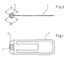
- the component of the switch in FIG. 1 is a stamped component 1 made of an electrically conductive material. In a portion of this stamped component 1, an electrical contact 2 is formed. This contact 2 is integrally connected to the other areas of the stamped component 1.
- Fig. 2 shows that the contact 2 has a hollow cylindrical shape.
- the contact 2 is arranged by rolling up in the front region of the stamped component 1 Material of the stamped component 1 is formed.
- the angles ⁇ and ⁇ ' indicate the surface areas of the contact 2 in which contact surfaces 3 of the contact 2 are located. With these areas, the contact 2 can be applied to a mating contact, not shown.
- the stamped component 1 consists for example of brass, which has a thickness of about 0.5 mm. In the area of the contact surface 3, a noble metal layer is introduced into the brass.
Abstract
Description
- Die Erfindung betrifft einen elektrischen Schalter, insbesondere einen elektrischen Mikroschalter, umfassend zumindest einen elektrischen Kontakt.
- Elektrische Schalter werden in elektrischen Stromkreisen zum Ein- und Ausschalten von elektrischen Verbrauchern eingesetzt. Häufig werden derartige Stromkreise miniaturisiert, auch um sie in komplexen technischen Einrichtungen integrieren zu können. Insbesondere im Fahrzeugbau werden miniaturisierte Schalter eingesetzt, welche die verschiedenen Funktionen in einem Fahrzeug steuern. Derartige Mikroschalter finden sich z.B. in Türschlössern, Motorhauben, Heckklappen und im Fahrzeuginnenraum.
- Elektrische Schalter, insbesondere Mikroschalter, weisen wenigstens einen elektrischen Kontakt auf, der an der Leitung des elektrischen Stromes unmittelbar beteiligt ist. Der Kontakt besteht dazu aus einem elektrisch leitfähigen Material, er ist an einen Gegenkontakt oder an andere elektrisch leitende Abschnitte anlegbar, um einen Stromfluß zu ermöglichen.
- Im Stand der Technik werden Kontakte eingesetzt, die aus Vollmaterial hergestellt sind. In einem weiteren Arbeitsschritt wird das Vollmaterial am Kontaktträger befestigt. Üblich ist ein Aufschweißen von Drahtabschnitten als Kontakt oder Einnieten von Kontakten in das Trägermaterial. Als Vollmaterial finden Silber (-Legierungen) oder Schichtwerkstoffe mit Silber- und Kupferanteilen Verwendung. Gemeinsam ist diesen Materialien eine geringe Härte.
- Die Kontakte aus Vollmaterial weisen eine erhöhte Masse auf, die aufgrund der hohen Dynamik des Schaltvorgangs Probleme bereitet. Ein Problem einer hohen Masse ist z.B., daß es bei einer Anlage an einem Gegenkontakt zum Auftreten von Schwingungen kommen kann, welche ein zeitweiliges Abheben des Kontaktes von dem Gegenkontakt bewirken. Dies insbesondere dann, wenn der Kontakt in beschleunigter Weise an den Gegenkontakt herangeführt wird. Bei einem derartigen Aufschlagen des Kontaktes kann es zu Impulserscheinungen kommen, die ein mehrfaches Abheben des Kontaktes bewirken, wodurch der eigentlich erwünschte Stromfluß unterbrochen wird.
- Der Erfindung liegt die Aufgabe zugrunde, einen elektrischen Schalter der eingangs genannten Gattung aufzuzeigen, bei dem das Auftreten von Schwingungen beim Heranführen an einen Gegenkontakt nicht gegeben ist.
- Diese Aufgabe ist erfindungsgemäß dadurch gelöst, daß der Kontakt als Hohlform-Abschnitt eines Bauteils aus elektrisch leitendem Material ausgebildet ist.
- Bei dem erfindungsgemäßen Schalter ist der Kontakt nicht aus einem vollen Material gefertigt. Vielmehr liegt eine Bauform als Hohlform-Abschnitt vor, wodurch auf vorteilhafte Weise eine äußere Gestaltung wie bei einem Kontakt aus vollem Material ermöglicht ist, wobei aber auf der Gegenseite eine deutliche Reduzierung der Masse des Kontaktes erreicht ist. Dieser massereduzierte Kontakt stellt somit die gleiche elektrische Kontaktfläche wie beim Stand der Technik zur Verfügung, allerdings ist bei ihm das Auftreten von Schwingungen beim Aufschlagen auf einen Gegenkontakt nicht gegeben. Der erfindungsgemäße Kontakt weist nämlich nicht die für das Auftreten von Impulsen erforderliche Masse auf. Die Masse des Hohlform-Kontaktes ist nämlich gegenüber einem Kontakt aus vollem Material deutlich reduziert.
- Nach einer ersten Weiterbildung der Erfindung ist vorgesehen, daß der Kontakt eine Hohlzylinderform aufweist. Durch die Hohlzylinderform wird mit dem Mantel des Zylinders eine Kontaktfläche ausgebildet, die sich an verschieden ausgebildete Gegenkontakte anlegen kann. Der Gegenkontakt kann vorzugsweise auch eine Zylinderform aufweisen, beide Längsachsen der Zylinder können dabei um einen Winkel von etwa 90° zueinander verlaufen. Gegenkontakt und Kontakt bilden dann eine optimale punktförmige (bei Berücksichtigung der Abplattung kreisförmige) Kontaktstelle, die ihre optimale Form auch bei Winkelfehlern der beteiligten Kontakte beibehält.
- Zur weiteren Ausbildung der Erfindung kann vorgesehen sein, daß die Hohlform aus einem planen Material durch ein Umformen desselben ausgebildet ist. Das plane Material kann ein elektrisch leitendes Material sein, das beispielsweise durch einen Stanzvorgang ausgebildet wurde. Bei dem erfindungsgemäßen Schalter ist an dieses plane Material kein von außen zuzuführender Kontakt aus vollem Material anzubringen, sondern der als Hohlzylinderform ausgebildete Kontakt kann z.B. durch ein Aufrollen des Materials selbst gebildet werden. Dadurch ist auch die Herstellung des erfindungsgemäßen elektrischen Schalters vereinfacht.
- Die Festkontakte können ebenfalls durch Umformen ohne zusätzliches Vollmaterial gebildet werden.
- Erfindungsgemäß wird ein Arbeitsschritt (Fügen des Vollmaterials an den Träger) bei der Herstellung eingespart sowie insgesamt das Kontaktverhalten gegenüber dem Stand der Technik verbessert. Weiches Material wird nicht aufgetragen, das härtere Grundmaterial hält den mechanischen Beanspruchungen beim Schaltstoß besser stand. Es kommt zu keinen oder nur minimalen plastischen Verformungen. Bei Schalten kommt es zu Relativbewegungen der Kontaktfläche. Härtere Flächen widerstehen dem daraus resultierenden Reibverschleiß besser. Werden die Kontaktflächen wie vorgeschlagen durch Umformen gebildet (z. B. rollen, prägen ) so ergibt sich eine weitere Härtezunahme infolge des Umformprozesses.
- Nach dem Stand der Technik werden Kontakte, die niedrige Ströme leiten (Steuerströme) mit einer Edelmetallschicht, vorzugsweise Gold(-Legierungen), versehen. Bei dem verwendeten Vollmaterial wird typischerweise eine größere Fläche veredelt, als für die Schaltfunktion erforderlich ist und z.B. mit einer Edelmetallschicht versehen.
- Nach einer Weiterbildung der Erfindung wird eine Edelmetallschicht selektiv nur in den an der Funktion beteiligten Bereichen aufgebracht, wodurch Edelmetall eingespart wird. Bei der erfindungsgemäßen Gestaltung haben die Kontaktflächen eine größere Härte als bei dem Vollmaterial. Die höhere Härte ermöglicht eine Reduzierung der Schichtdicke. Bei bestimmten Anwendungen kann bei dieser Ausführung einseitig die Edelmetallschicht weggelassen werden oder als reiner Transportschutz auf ein äußerstes Minimum reduziert werden, da sich die funktionell nötige Edelmetallschicht durch Materialübertragung vom Gegenkontakt ergibt. Die so gebildeten Kontaktflächen sind für die elektrischen und mechanischen Beanspruchungen besser geeignet als Kontaktflächen aus Vollmaterial.
- Ein Ausführungsbeispiel der Erfindung, aus dem sich weitere erfinderische Merkmale ergeben, ist in der Zeichnung dargestellt. Es zeigen:
- Fig. 1:
- eine Draufsicht eines Bauteils eines elektrischen Schalters mit einem elektrischen Kontakt und
- Fig. 2:
- eine Seitenansicht eines Bauteils gemäß Fig. 1
- Bei dem Bauteil des Schalters in Fig. 1 handelt es sich um ein Stanzbauteil 1 aus einem elektrisch leitenden Material. In einem Abschnitt dieses Stanzbauteils 1 ist ein elektrischer Kontakt 2 ausgebildet. Dieser Kontakt 2 ist mit den übrigen Bereichen des Stanzbauteils 1 einstückig verbunden.
- Fig. 2 zeigt, daß der Kontakt 2 eine Hohlzylinderform aufweist. Der Kontakt 2 ist durch ein Aufrollen des im Stirnbereich des Stanzbauteils 1 angeordneten Materials des Stanzbauteils 1 ausgebildet. Die Winkel α und α' zeigen die Oberflächenbereiche des Kontaktes 2 an, in denen sich Kontaktoberflächen 3 des Kontaktes 2 befinden. Mit diesen Bereichen kann der Kontakt 2 an einen nicht weiter dargestellten Gegenkontakt angelegt werden.
- Das Stanzbauteil 1 besteht beispielsweise aus Messing, welches eine Dicke von ca. 0,5 mm aufweist. Im Bereich der Kontaktoberfläche 3 ist in das Messing eine Edelmetallschicht eingebracht.
Claims (6)
- Elektrischer Schalter, insbesondere elektrischer Mikroschalter, umfassend zumindest einen elektrischen Kontakt,
dadurch gekennzeichnet,
daß der Kontakt (2) als Hohlform-Abschnitt eines Bauteils (1) aus elektrisch leitendem Material ausgebildet ist. - Schalter nach Anspruch 1, dadurch gekennzeichnet, daß der Kontakt (2) eine Hohlzylinderform aufweist.
- Schalter nach Anspruch 1 oder 2, dadurch gekennzeichnet, daß die Hohlform aus einem planen Material durch ein Umformen desselben ausgebildet ist.
- Schalter nach einem der vorhergehenden Ansprüche, dadurch gekennzeichnet, daß der Kontakt (2) wenigstens eine Kontaktoberfläche (3) aufweist, in welche eine Edelmetallschicht selektiv eingebracht ist.
- Schalter nach Anspruch 4, dadurch gekennzeichnet, daß die Edelmetallschicht auf die Kontaktoberfläche (3) nur einseitig aufgebracht ist.
- Schalter nach einem der vorhergehenden Ansprüche, dadurch gekennzeichnet, daß das Bauteil (1) ein Stanzbauteil ist, an welches der Kontakt (2) einstückig angeformt ist.
Priority Applications (1)
| Application Number | Priority Date | Filing Date | Title |
|---|---|---|---|
| PL07017931T PL1903585T3 (pl) | 2006-09-19 | 2007-09-13 | Zestyk przełączający ze sprężyną stykową o zmniejszonym ciężarze |
Applications Claiming Priority (1)
| Application Number | Priority Date | Filing Date | Title |
|---|---|---|---|
| DE102006043795A DE102006043795B3 (de) | 2006-09-19 | 2006-09-19 | Elektrischer Mikroschalter |
Publications (3)
| Publication Number | Publication Date |
|---|---|
| EP1903585A2 true EP1903585A2 (de) | 2008-03-26 |
| EP1903585A3 EP1903585A3 (de) | 2008-12-31 |
| EP1903585B1 EP1903585B1 (de) | 2015-10-07 |
Family
ID=38646569
Family Applications (1)
| Application Number | Title | Priority Date | Filing Date |
|---|---|---|---|
| EP07017931.2A Active EP1903585B1 (de) | 2006-09-19 | 2007-09-13 | Schaltkontakt mit gewichtsreduzierter Kontaktfeder |
Country Status (6)
| Country | Link |
|---|---|
| US (3) | US20080156625A1 (de) |
| EP (1) | EP1903585B1 (de) |
| DE (1) | DE102006043795B3 (de) |
| ES (1) | ES2558307T3 (de) |
| HU (1) | HUE028229T2 (de) |
| PL (1) | PL1903585T3 (de) |
Cited By (1)
| Publication number | Priority date | Publication date | Assignee | Title |
|---|---|---|---|---|
| CN104616922A (zh) * | 2013-11-05 | 2015-05-13 | 德昌电机(深圳)有限公司 | 快动开关 |
Families Citing this family (3)
| Publication number | Priority date | Publication date | Assignee | Title |
|---|---|---|---|---|
| DE102008035043B4 (de) * | 2008-07-26 | 2013-04-04 | Johnson Electric Oldenburg Gmbh & Co. Kg | Mikroschalter |
| DE102011088793A1 (de) * | 2011-12-16 | 2013-06-20 | Tyco Electronics Amp Gmbh | Elektrischer Steckverbinder mit mikrostrukturiertem Kontaktelement |
| DE102014006033A1 (de) * | 2014-02-15 | 2015-08-20 | Johnson Electric Germany GmbH & Co. KG | Elektrischer Mikroschalter, umfassend zumindest einen elektrischen Kontakt und Verfahren zum Herstellen eines elektrischen Mikroschalters |
Citations (1)
| Publication number | Priority date | Publication date | Assignee | Title |
|---|---|---|---|---|
| FR2504311A1 (fr) | 1981-04-15 | 1982-10-22 | Telemecanique Electrique | Interrupteur electrique operant la fermeture et l'ouverture repetees d'un circuit electrique |
Family Cites Families (10)
| Publication number | Priority date | Publication date | Assignee | Title |
|---|---|---|---|---|
| DE1829459U (de) | 1959-08-01 | 1961-04-13 | Continental Elektro Ind Ag | Schaltstueckanordnung fuer leistungsschalter. |
| AT337818B (de) * | 1975-03-19 | 1977-07-25 | Reiter Lothar Dipl Ing Dr Tech | Prellfreie massenanordnung |
| DE7527477U (de) | 1975-08-30 | 1977-02-03 | Standard Elektrik Lorenz Ag, 7000 Stuttgart | Einseitig befestigte Kontaktfeder |
| DE3328360A1 (de) * | 1983-08-03 | 1985-02-21 | Siemens AG, 1000 Berlin und 8000 München | Kontaktanordnung fuer drehschalter |
| DE3427261C2 (de) * | 1983-08-31 | 1986-05-22 | Hosiden Electronics Co., Ltd., Osaka | Elektrische Anschlußbuchse |
| JPH0297771U (de) * | 1989-01-17 | 1990-08-03 | ||
| JP3598811B2 (ja) * | 1998-05-14 | 2004-12-08 | 住友電装株式会社 | 短絡端子とこれを組み込んだ嵌合検知用コネクタ |
| DE10246062A1 (de) * | 2002-10-02 | 2004-04-15 | Robert Bosch Gmbh | Elektrischer Kontakt |
| TW591829B (en) * | 2003-05-09 | 2004-06-11 | Benq Corp | Connection device for selectably retrieving signals |
| JP4451748B2 (ja) * | 2004-09-17 | 2010-04-14 | 株式会社東海理化電機製作所 | スライドスイッチ |
-
2006
- 2006-09-19 DE DE102006043795A patent/DE102006043795B3/de not_active Expired - Fee Related
-
2007
- 2007-09-13 PL PL07017931T patent/PL1903585T3/pl unknown
- 2007-09-13 ES ES07017931.2T patent/ES2558307T3/es active Active
- 2007-09-13 EP EP07017931.2A patent/EP1903585B1/de active Active
- 2007-09-13 HU HUE07017931A patent/HUE028229T2/en unknown
- 2007-09-18 US US11/901,627 patent/US20080156625A1/en not_active Abandoned
-
2010
- 2010-12-15 US US12/969,109 patent/US8053693B2/en not_active Expired - Fee Related
-
2011
- 2011-08-17 US US13/211,843 patent/US9589740B2/en active Active
Patent Citations (1)
| Publication number | Priority date | Publication date | Assignee | Title |
|---|---|---|---|---|
| FR2504311A1 (fr) | 1981-04-15 | 1982-10-22 | Telemecanique Electrique | Interrupteur electrique operant la fermeture et l'ouverture repetees d'un circuit electrique |
Cited By (1)
| Publication number | Priority date | Publication date | Assignee | Title |
|---|---|---|---|---|
| CN104616922A (zh) * | 2013-11-05 | 2015-05-13 | 德昌电机(深圳)有限公司 | 快动开关 |
Also Published As
| Publication number | Publication date |
|---|---|
| DE102006043795B3 (de) | 2008-05-29 |
| US20080156625A1 (en) | 2008-07-03 |
| US8053693B2 (en) | 2011-11-08 |
| ES2558307T3 (es) | 2016-02-03 |
| US20110083947A1 (en) | 2011-04-14 |
| HUE028229T2 (en) | 2016-12-28 |
| EP1903585B1 (de) | 2015-10-07 |
| US9589740B2 (en) | 2017-03-07 |
| PL1903585T3 (pl) | 2016-03-31 |
| US20110297520A1 (en) | 2011-12-08 |
| EP1903585A3 (de) | 2008-12-31 |
Similar Documents
| Publication | Publication Date | Title |
|---|---|---|
| DE102013105571A1 (de) | Kontaktelement zur Kontaktierung mindestens eines Wicklungsdrahts | |
| EP0374648A2 (de) | Vorrichtung zum Anschluss eines eletrischen Kabels | |
| DE112013007018T5 (de) | Nietenkontakt und Verfahren zu dessen Herstellung | |
| EP1903585B1 (de) | Schaltkontakt mit gewichtsreduzierter Kontaktfeder | |
| WO2020058138A1 (de) | Steckverbindung mit redundanz sowie fahrzeug mit einer solchen | |
| EP2524384B1 (de) | Elektrisches kontaktelement und verfahren zur herstellung eines elektrischen kontaktelements | |
| EP3482460A1 (de) | Elektrischer hochleistungskontakt | |
| EP2297820A1 (de) | Schutzleiteranschlussvorrichtung aus metall | |
| EP2437360A1 (de) | Stockwerksbrücker | |
| DE1924701A1 (de) | Thermisch ansprechender Schnappschalter | |
| EP3871293B1 (de) | Elektrisches kontaktelement | |
| DE102012204371A1 (de) | Kontaktanordnung und elektrisches Schaltgerät | |
| DE102004058640B3 (de) | NH-Kontakt | |
| DE102018202187A1 (de) | Strompfadteil für ein elektrisches Schaltgerät | |
| EP0433802B1 (de) | Hochstrom-Steckverbindersatz mit zwei langgestreckten Zwittersteckern | |
| EP1365487B1 (de) | Verfahren zur Herstellung eines Gehäuses | |
| DE102022107669B4 (de) | Steckverbindung, insbesondere für eine Gleichstromverbindung, Steckkontakt und Verfahren zu dessen Herstellung | |
| EP3673497B1 (de) | Abtrennvorrichtung für einen überspannungsableiter | |
| EP3176798B1 (de) | Kontaktsystem eines elektrischen installationsschalters | |
| EP4002592A1 (de) | Anschlussteil für eine elektrische leitung und leitungsverbindung | |
| EP1508941B1 (de) | Elektrischer Leiter mit einem Lotdepot an einem Kontaktabschnitt | |
| DE102005018144B4 (de) | Elektrische Schalteranordnung | |
| WO1991006964A1 (de) | Kontaktanordnung für ein wechsler-relais | |
| DE102013015088A1 (de) | Elektrisches Kontaktelement für einen mechanisch schaltbaren elektrischen Schaltkontakt und Verfahren zu dessen Herstellung | |
| EP3871294A1 (de) | Elektrisches kontaktelement für hohe betriebsspannungen |
Legal Events
| Date | Code | Title | Description |
|---|---|---|---|
| PUAI | Public reference made under article 153(3) epc to a published international application that has entered the european phase |
Free format text: ORIGINAL CODE: 0009012 |
|
| AK | Designated contracting states |
Kind code of ref document: A2 Designated state(s): AT BE BG CH CY CZ DE DK EE ES FI FR GB GR HU IE IS IT LI LT LU LV MC MT NL PL PT RO SE SI SK TR |
|
| AX | Request for extension of the european patent |
Extension state: AL BA HR MK YU |
|
| RIN1 | Information on inventor provided before grant (corrected) |
Inventor name: BERTRAM, ROLF Inventor name: STENZEL, BRUNO Inventor name: KOEPSELL, MARTIN |
|
| PUAL | Search report despatched |
Free format text: ORIGINAL CODE: 0009013 |
|
| AK | Designated contracting states |
Kind code of ref document: A3 Designated state(s): AT BE BG CH CY CZ DE DK EE ES FI FR GB GR HU IE IS IT LI LT LU LV MC MT NL PL PT RO SE SI SK TR |
|
| AX | Request for extension of the european patent |
Extension state: AL BA HR MK RS |
|
| 17P | Request for examination filed |
Effective date: 20090528 |
|
| 17Q | First examination report despatched |
Effective date: 20090625 |
|
| AKX | Designation fees paid |
Designated state(s): AT BE BG CH CY CZ DE DK EE ES FI FR GB GR HU IE IS IT LI LT LU LV MC MT NL PL PT RO SE SI SK TR |
|
| RAP1 | Party data changed (applicant data changed or rights of an application transferred) |
Owner name: JOHNSON ELECTRIC OLDENBURG GMBH & CO. KG |
|
| RAP1 | Party data changed (applicant data changed or rights of an application transferred) |
Owner name: JOHNSON ELECTRIC GERMANY GMBH & CO. KG |
|
| GRAP | Despatch of communication of intention to grant a patent |
Free format text: ORIGINAL CODE: EPIDOSNIGR1 |
|
| INTG | Intention to grant announced |
Effective date: 20150710 |
|
| GRAS | Grant fee paid |
Free format text: ORIGINAL CODE: EPIDOSNIGR3 |
|
| GRAA | (expected) grant |
Free format text: ORIGINAL CODE: 0009210 |
|
| AK | Designated contracting states |
Kind code of ref document: B1 Designated state(s): AT BE BG CH CY CZ DE DK EE ES FI FR GB GR HU IE IS IT LI LT LU LV MC MT NL PL PT RO SE SI SK TR |
|
| REG | Reference to a national code |
Ref country code: GB Ref legal event code: FG4D Free format text: NOT ENGLISH |
|
| REG | Reference to a national code |
Ref country code: AT Ref legal event code: REF Ref document number: 754180 Country of ref document: AT Kind code of ref document: T Effective date: 20151015 Ref country code: CH Ref legal event code: EP |
|
| REG | Reference to a national code |
Ref country code: IE Ref legal event code: FG4D Free format text: LANGUAGE OF EP DOCUMENT: GERMAN |
|
| REG | Reference to a national code |
Ref country code: DE Ref legal event code: R096 Ref document number: 502007014282 Country of ref document: DE |
|
| REG | Reference to a national code |
Ref country code: SE Ref legal event code: TRGR |
|
| REG | Reference to a national code |
Ref country code: ES Ref legal event code: FG2A Ref document number: 2558307 Country of ref document: ES Kind code of ref document: T3 Effective date: 20160203 |
|
| REG | Reference to a national code |
Ref country code: LT Ref legal event code: MG4D |
|
| REG | Reference to a national code |
Ref country code: NL Ref legal event code: FP |
|
| PG25 | Lapsed in a contracting state [announced via postgrant information from national office to epo] |
Ref country code: IS Free format text: LAPSE BECAUSE OF FAILURE TO SUBMIT A TRANSLATION OF THE DESCRIPTION OR TO PAY THE FEE WITHIN THE PRESCRIBED TIME-LIMIT Effective date: 20160207 Ref country code: LT Free format text: LAPSE BECAUSE OF FAILURE TO SUBMIT A TRANSLATION OF THE DESCRIPTION OR TO PAY THE FEE WITHIN THE PRESCRIBED TIME-LIMIT Effective date: 20151007 |
|
| PG25 | Lapsed in a contracting state [announced via postgrant information from national office to epo] |
Ref country code: PT Free format text: LAPSE BECAUSE OF FAILURE TO SUBMIT A TRANSLATION OF THE DESCRIPTION OR TO PAY THE FEE WITHIN THE PRESCRIBED TIME-LIMIT Effective date: 20160208 Ref country code: FI Free format text: LAPSE BECAUSE OF FAILURE TO SUBMIT A TRANSLATION OF THE DESCRIPTION OR TO PAY THE FEE WITHIN THE PRESCRIBED TIME-LIMIT Effective date: 20151007 Ref country code: LV Free format text: LAPSE BECAUSE OF FAILURE TO SUBMIT A TRANSLATION OF THE DESCRIPTION OR TO PAY THE FEE WITHIN THE PRESCRIBED TIME-LIMIT Effective date: 20151007 Ref country code: GR Free format text: LAPSE BECAUSE OF FAILURE TO SUBMIT A TRANSLATION OF THE DESCRIPTION OR TO PAY THE FEE WITHIN THE PRESCRIBED TIME-LIMIT Effective date: 20160108 |
|
| REG | Reference to a national code |
Ref country code: DE Ref legal event code: R097 Ref document number: 502007014282 Country of ref document: DE |
|
| PG25 | Lapsed in a contracting state [announced via postgrant information from national office to epo] |
Ref country code: CZ Free format text: LAPSE BECAUSE OF FAILURE TO SUBMIT A TRANSLATION OF THE DESCRIPTION OR TO PAY THE FEE WITHIN THE PRESCRIBED TIME-LIMIT Effective date: 20151007 |
|
| PLBE | No opposition filed within time limit |
Free format text: ORIGINAL CODE: 0009261 |
|
| STAA | Information on the status of an ep patent application or granted ep patent |
Free format text: STATUS: NO OPPOSITION FILED WITHIN TIME LIMIT |
|
| PG25 | Lapsed in a contracting state [announced via postgrant information from national office to epo] |
Ref country code: SK Free format text: LAPSE BECAUSE OF FAILURE TO SUBMIT A TRANSLATION OF THE DESCRIPTION OR TO PAY THE FEE WITHIN THE PRESCRIBED TIME-LIMIT Effective date: 20151007 Ref country code: EE Free format text: LAPSE BECAUSE OF FAILURE TO SUBMIT A TRANSLATION OF THE DESCRIPTION OR TO PAY THE FEE WITHIN THE PRESCRIBED TIME-LIMIT Effective date: 20151007 Ref country code: DK Free format text: LAPSE BECAUSE OF FAILURE TO SUBMIT A TRANSLATION OF THE DESCRIPTION OR TO PAY THE FEE WITHIN THE PRESCRIBED TIME-LIMIT Effective date: 20151007 Ref country code: RO Free format text: LAPSE BECAUSE OF FAILURE TO SUBMIT A TRANSLATION OF THE DESCRIPTION OR TO PAY THE FEE WITHIN THE PRESCRIBED TIME-LIMIT Effective date: 20151007 |
|
| 26N | No opposition filed |
Effective date: 20160708 |
|
| REG | Reference to a national code |
Ref country code: FR Ref legal event code: PLFP Year of fee payment: 10 |
|
| PG25 | Lapsed in a contracting state [announced via postgrant information from national office to epo] |
Ref country code: SI Free format text: LAPSE BECAUSE OF FAILURE TO SUBMIT A TRANSLATION OF THE DESCRIPTION OR TO PAY THE FEE WITHIN THE PRESCRIBED TIME-LIMIT Effective date: 20151007 |
|
| REG | Reference to a national code |
Ref country code: HU Ref legal event code: AG4A Ref document number: E028229 Country of ref document: HU |
|
| PG25 | Lapsed in a contracting state [announced via postgrant information from national office to epo] |
Ref country code: BE Free format text: LAPSE BECAUSE OF NON-PAYMENT OF DUE FEES Effective date: 20160930 |
|
| PG25 | Lapsed in a contracting state [announced via postgrant information from national office to epo] |
Ref country code: MC Free format text: LAPSE BECAUSE OF FAILURE TO SUBMIT A TRANSLATION OF THE DESCRIPTION OR TO PAY THE FEE WITHIN THE PRESCRIBED TIME-LIMIT Effective date: 20151007 |
|
| REG | Reference to a national code |
Ref country code: CH Ref legal event code: PL |
|
| REG | Reference to a national code |
Ref country code: IE Ref legal event code: MM4A |
|
| PG25 | Lapsed in a contracting state [announced via postgrant information from national office to epo] |
Ref country code: IE Free format text: LAPSE BECAUSE OF NON-PAYMENT OF DUE FEES Effective date: 20160913 Ref country code: CH Free format text: LAPSE BECAUSE OF NON-PAYMENT OF DUE FEES Effective date: 20160930 Ref country code: LI Free format text: LAPSE BECAUSE OF NON-PAYMENT OF DUE FEES Effective date: 20160930 |
|
| PG25 | Lapsed in a contracting state [announced via postgrant information from national office to epo] |
Ref country code: LU Free format text: LAPSE BECAUSE OF NON-PAYMENT OF DUE FEES Effective date: 20160913 |
|
| REG | Reference to a national code |
Ref country code: FR Ref legal event code: PLFP Year of fee payment: 11 |
|
| REG | Reference to a national code |
Ref country code: AT Ref legal event code: MM01 Ref document number: 754180 Country of ref document: AT Kind code of ref document: T Effective date: 20160913 |
|
| REG | Reference to a national code |
Ref country code: BE Ref legal event code: MM Effective date: 20160930 |
|
| PG25 | Lapsed in a contracting state [announced via postgrant information from national office to epo] |
Ref country code: AT Free format text: LAPSE BECAUSE OF NON-PAYMENT OF DUE FEES Effective date: 20160913 |
|
| PG25 | Lapsed in a contracting state [announced via postgrant information from national office to epo] |
Ref country code: CY Free format text: LAPSE BECAUSE OF FAILURE TO SUBMIT A TRANSLATION OF THE DESCRIPTION OR TO PAY THE FEE WITHIN THE PRESCRIBED TIME-LIMIT Effective date: 20151007 |
|
| PG25 | Lapsed in a contracting state [announced via postgrant information from national office to epo] |
Ref country code: MT Free format text: LAPSE BECAUSE OF FAILURE TO SUBMIT A TRANSLATION OF THE DESCRIPTION OR TO PAY THE FEE WITHIN THE PRESCRIBED TIME-LIMIT Effective date: 20151007 |
|
| PG25 | Lapsed in a contracting state [announced via postgrant information from national office to epo] |
Ref country code: BG Free format text: LAPSE BECAUSE OF FAILURE TO SUBMIT A TRANSLATION OF THE DESCRIPTION OR TO PAY THE FEE WITHIN THE PRESCRIBED TIME-LIMIT Effective date: 20151007 |
|
| REG | Reference to a national code |
Ref country code: FR Ref legal event code: PLFP Year of fee payment: 12 |
|
| PGFP | Annual fee paid to national office [announced via postgrant information from national office to epo] |
Ref country code: TR Payment date: 20210910 Year of fee payment: 15 |
|
| PGFP | Annual fee paid to national office [announced via postgrant information from national office to epo] |
Ref country code: ES Payment date: 20211005 Year of fee payment: 15 |
|
| PGFP | Annual fee paid to national office [announced via postgrant information from national office to epo] |
Ref country code: NL Payment date: 20220715 Year of fee payment: 16 |
|
| PGFP | Annual fee paid to national office [announced via postgrant information from national office to epo] |
Ref country code: SE Payment date: 20220714 Year of fee payment: 16 Ref country code: IT Payment date: 20220811 Year of fee payment: 16 Ref country code: GB Payment date: 20220721 Year of fee payment: 16 |
|
| PGFP | Annual fee paid to national office [announced via postgrant information from national office to epo] |
Ref country code: PL Payment date: 20220712 Year of fee payment: 16 Ref country code: HU Payment date: 20220806 Year of fee payment: 16 Ref country code: FR Payment date: 20220709 Year of fee payment: 16 |
|
| REG | Reference to a national code |
Ref country code: DE Ref legal event code: R084 Ref document number: 502007014282 Country of ref document: DE |
|
| P01 | Opt-out of the competence of the unified patent court (upc) registered |
Effective date: 20230628 |
|
| REG | Reference to a national code |
Ref country code: ES Ref legal event code: FD2A Effective date: 20231027 |
|
| PGFP | Annual fee paid to national office [announced via postgrant information from national office to epo] |
Ref country code: DE Payment date: 20230928 Year of fee payment: 17 |
|
| PG25 | Lapsed in a contracting state [announced via postgrant information from national office to epo] |
Ref country code: ES Free format text: LAPSE BECAUSE OF NON-PAYMENT OF DUE FEES Effective date: 20220914 |
|
| PG25 | Lapsed in a contracting state [announced via postgrant information from national office to epo] |
Ref country code: ES Free format text: LAPSE BECAUSE OF NON-PAYMENT OF DUE FEES Effective date: 20220914 |