EP1941484B1 - Illumination device - Google Patents
Illumination device Download PDFInfo
- Publication number
- EP1941484B1 EP1941484B1 EP06809556A EP06809556A EP1941484B1 EP 1941484 B1 EP1941484 B1 EP 1941484B1 EP 06809556 A EP06809556 A EP 06809556A EP 06809556 A EP06809556 A EP 06809556A EP 1941484 B1 EP1941484 B1 EP 1941484B1
- Authority
- EP
- European Patent Office
- Prior art keywords
- area
- illumination
- active
- value
- illumination area
- Prior art date
- Legal status (The legal status is an assumption and is not a legal conclusion. Google has not performed a legal analysis and makes no representation as to the accuracy of the status listed.)
- Not-in-force
Links
Images
Classifications
-
- G—PHYSICS
- G09—EDUCATION; CRYPTOGRAPHY; DISPLAY; ADVERTISING; SEALS
- G09G—ARRANGEMENTS OR CIRCUITS FOR CONTROL OF INDICATING DEVICES USING STATIC MEANS TO PRESENT VARIABLE INFORMATION
- G09G3/00—Control arrangements or circuits, of interest only in connection with visual indicators other than cathode-ray tubes
- G09G3/20—Control arrangements or circuits, of interest only in connection with visual indicators other than cathode-ray tubes for presentation of an assembly of a number of characters, e.g. a page, by composing the assembly by combination of individual elements arranged in a matrix no fixed position being assigned to or needed to be assigned to the individual characters or partial characters
- G09G3/22—Control arrangements or circuits, of interest only in connection with visual indicators other than cathode-ray tubes for presentation of an assembly of a number of characters, e.g. a page, by composing the assembly by combination of individual elements arranged in a matrix no fixed position being assigned to or needed to be assigned to the individual characters or partial characters using controlled light sources
- G09G3/30—Control arrangements or circuits, of interest only in connection with visual indicators other than cathode-ray tubes for presentation of an assembly of a number of characters, e.g. a page, by composing the assembly by combination of individual elements arranged in a matrix no fixed position being assigned to or needed to be assigned to the individual characters or partial characters using controlled light sources using electroluminescent panels
- G09G3/32—Control arrangements or circuits, of interest only in connection with visual indicators other than cathode-ray tubes for presentation of an assembly of a number of characters, e.g. a page, by composing the assembly by combination of individual elements arranged in a matrix no fixed position being assigned to or needed to be assigned to the individual characters or partial characters using controlled light sources using electroluminescent panels semiconductive, e.g. using light-emitting diodes [LED]
- G09G3/3208—Control arrangements or circuits, of interest only in connection with visual indicators other than cathode-ray tubes for presentation of an assembly of a number of characters, e.g. a page, by composing the assembly by combination of individual elements arranged in a matrix no fixed position being assigned to or needed to be assigned to the individual characters or partial characters using controlled light sources using electroluminescent panels semiconductive, e.g. using light-emitting diodes [LED] organic, e.g. using organic light-emitting diodes [OLED]
-
- H—ELECTRICITY
- H01—ELECTRIC ELEMENTS
- H01L—SEMICONDUCTOR DEVICES NOT COVERED BY CLASS H10
- H01L21/00—Processes or apparatus adapted for the manufacture or treatment of semiconductor or solid state devices or of parts thereof
- H01L21/02—Manufacture or treatment of semiconductor devices or of parts thereof
- H01L21/04—Manufacture or treatment of semiconductor devices or of parts thereof the devices having at least one potential-jump barrier or surface barrier, e.g. PN junction, depletion layer or carrier concentration layer
- H01L21/06—Manufacture or treatment of semiconductor devices or of parts thereof the devices having at least one potential-jump barrier or surface barrier, e.g. PN junction, depletion layer or carrier concentration layer the devices having semiconductor bodies comprising selenium or tellurium in uncombined form other than as impurities in semiconductor bodies of other materials
- H01L21/14—Treatment of the complete device, e.g. by electroforming to form a barrier
- H01L21/145—Ageing
-
- H—ELECTRICITY
- H05—ELECTRIC TECHNIQUES NOT OTHERWISE PROVIDED FOR
- H05B—ELECTRIC HEATING; ELECTRIC LIGHT SOURCES NOT OTHERWISE PROVIDED FOR; CIRCUIT ARRANGEMENTS FOR ELECTRIC LIGHT SOURCES, IN GENERAL
- H05B45/00—Circuit arrangements for operating light-emitting diodes [LED]
- H05B45/60—Circuit arrangements for operating LEDs comprising organic material, e.g. for operating organic light-emitting diodes [OLED] or polymer light-emitting diodes [PLED]
-
- G—PHYSICS
- G09—EDUCATION; CRYPTOGRAPHY; DISPLAY; ADVERTISING; SEALS
- G09G—ARRANGEMENTS OR CIRCUITS FOR CONTROL OF INDICATING DEVICES USING STATIC MEANS TO PRESENT VARIABLE INFORMATION
- G09G2320/00—Control of display operating conditions
- G09G2320/02—Improving the quality of display appearance
- G09G2320/029—Improving the quality of display appearance by monitoring one or more pixels in the display panel, e.g. by monitoring a fixed reference pixel
-
- G—PHYSICS
- G09—EDUCATION; CRYPTOGRAPHY; DISPLAY; ADVERTISING; SEALS
- G09G—ARRANGEMENTS OR CIRCUITS FOR CONTROL OF INDICATING DEVICES USING STATIC MEANS TO PRESENT VARIABLE INFORMATION
- G09G2320/00—Control of display operating conditions
- G09G2320/04—Maintaining the quality of display appearance
- G09G2320/043—Preventing or counteracting the effects of ageing
-
- Y—GENERAL TAGGING OF NEW TECHNOLOGICAL DEVELOPMENTS; GENERAL TAGGING OF CROSS-SECTIONAL TECHNOLOGIES SPANNING OVER SEVERAL SECTIONS OF THE IPC; TECHNICAL SUBJECTS COVERED BY FORMER USPC CROSS-REFERENCE ART COLLECTIONS [XRACs] AND DIGESTS
- Y02—TECHNOLOGIES OR APPLICATIONS FOR MITIGATION OR ADAPTATION AGAINST CLIMATE CHANGE
- Y02B—CLIMATE CHANGE MITIGATION TECHNOLOGIES RELATED TO BUILDINGS, e.g. HOUSING, HOUSE APPLIANCES OR RELATED END-USER APPLICATIONS
- Y02B20/00—Energy efficient lighting technologies, e.g. halogen lamps or gas discharge lamps
- Y02B20/30—Semiconductor lamps, e.g. solid state lamps [SSL] light emitting diodes [LED] or organic LED [OLED]
Definitions
- the present invention relates to an illumination device comprising an organic light-emitting diode (OLED) having a light output that changes with use.
- OLED organic light-emitting diode
- Illumination devices with organic light-emitting diodes are of great interest as superior flat-panel systems. Theses systems utilize current passing through thin layers of organic material to generate light. The color of light emitted and the efficiency of the energy conversion from current to light are determined by the composition of the organic material. However, as the OLED is used, the organic materials in the illumination device age and become less efficient at emitting light. This reduces the lifetime of the illumination device.
- US 2004/0070558 A1 describes an organic light-emitting diode (OLED) display system having addressable pixels on a substrate, the pixels having performance attributes, and a control circuit for controlling the pixels of the display device, comprising one or more OLED pixels and an OLED reference pixel located on a substrate and connected to the control circuit.
- the OLED reference pixel comprise the same performance attribute as the one or more OLED pixel, wherein the OLED reference pixel have voltage sensing circuit including a transistor connected to one of the terminals of the OLED reference pixel for sensing the voltage across the OLED reference pixel to produce a voltage signal representing the voltage across the OLED reference pixel.
- the organic light-emitting diode comprises a measurement circuit to produce an output signal representative of the performance attribute of the OLED reference pixel and an analyse circuit connected to the measurement circuit to receive the output signal, comparing the performance attributes with predetermined performance attributes, and producing a feedback signal in response thereto.
- the said control circuit is responsive to the feedback signal to compensate for changes in the output of the OLED pixels.
- the described OLED display system making use of reference pixels to compensate aging effects is restricted to displays. Large area OLED devices for illumination, however, are not pixelated. Thus, the proposed device and method in US 2004/0070558 cannot be applied for non-pixelated illumination areas.
- US 6,081,073 and US 6,320,325 describes the use of sensors to measure the light output.
- One of the essential disadvantages is that the use of additional sensors generate more costs, moreover, the degradation issue is not solved but shifted to the sensor.
- the invention has for its object to eliminate the above mentioned disadvantages.
- an illumination device comprising an organic light-emitting diode (OLED) having a light output that changes with use with an illumination area, where light is being emitted for an illumination purpose.
- the illumination device includes a reference area being substantially smaller than the illumination area and a substrate, on which the illumination area and the reference area are located.
- a driver is connected to the reference area and the illumination area comprising a measurement and a control circuit to drive the reference area separately to the illumination area and/or active area.
- the measurement circuit detects at least one active value of the illumination area and at least one reference value of the reference area.
- the control circuit is to compare the active and the reference value and to produce a correction signal in response thereto to compensate the changes in the light outputs of the illumination area, whereby the control circuit calculates the correction signal for the illumination area based on the active value and the reference value.
- the illumination device comprises an illumination area, which emits light for illumination purpose being always in use during the "normal" illumination process.
- the active area is the illumination area itself.
- the active area is an area of the illumination device, which is a reproduction of the illumination area (same layer stack), wherein the active area is always in use during the illumination process.
- the driver is connected with the illumination area, the reference area and the active area separately.
- the measurement circuit detects at least one active value of the illumination area and/or the active area.
- the active area emits light during the illumination process while the illumination area is also in use.
- the active area is the illumination area itself.
- the active area consists of any shape substantially smaller than the illumination area.
- the active area comprises a similar shape substantially smaller than the illumination area.
- the reference area is an area of the illumination device, which is a reproduction of the illumination area, wherein the reference area is never in use during the illumination process.
- the reference area can be of any shape substantially smaller than the illumination area.
- the reference area is of similar shape substantially smaller than the illumination area.
- the OLED device of this invention is typically provided over a supporting substrate where either the cathode or anode can be in contact with the substrate.
- the electrode in contact with the substrate is conventionally referred to as the bottom electrode.
- the bottom electrode is the anode, but this invention is not limited to that configuration.
- the substrate can either be transmissive or opaque.
- Substrates can include, but are not limited to, glass, plastic, semiconductor materials, silicone, ceramics, circuit board materials.
- the reference area is an isolated area not connected to the active area. That means that during the pure illumination process the reference area is switched-off, wherein the illumination area and/or the active area produces the light output. Only, when the control circuit is activated, the reference area is switched-on.
- the OLED is a bottom emitting device or a top emitting device, whereby the illumination device in combination with said OLED can be used in systems with controllable color. That means that the driver compares the characteristics of both areas to determine the amount of correction for the driving of the illumination area. These values are fed into the control circuitry, which adjusts the driving current to achieve constant light output.
- the driver includes a fixed device characteristic for estimating the correction signal.
- the fixed device characteristic can comprise a mathematic function and/or a lookup table in a microcontroller based control circuit.
- the compensation characteristic depends on the OLED device and can be changed programmatically.
- the amount of compensation to achieve a constant light output over lifetime can be realized in form of a controlling algorithm of as microcontroller based circuitry.
- the reference area which is not fed by the driving current during the normal illumination process, can be integrated with the illumination area, which is in a preferred embodiment the active area. That means that the reference area is an integral part of the active area in a sense that both areas are located on the same substrate.
- the advantage is that the reference area and the active area have more or less the same characteristics especially for aging aspects.
- the reference area is a smaller reproduction of the illumination area.
- the control circuit has to convert the detected active value or the reference value in order to compare both values.
- the control circuit compares the behaviour of the reference area to the behaviour of the active area.
- the active and the reference value are voltage values measured for constant driving current. Depending on the deviation of the measured values for the active area compared to the reference area the driving current is varied for constant light output.
- the active and the reference value can be a capacity value measured by the measurement circuit.
- the illumination area is the active area of the illumination device.
- the active area is a smaller reproduction of the illumination area, whereby the active area and the reference area are similar in a mathematical sense.
- Said active area is connected to the illumination area.
- the reference area is an isolated area being not connected to the illumination area.
- the dimensions of said areas are similar or equal, preferably.
- said comparability is maximized, if reference, active and illumination area are similar in the mathematical sense, i.e. congruent to the result of a uniform scaling.
- the reference area and/or active area are located at the border of the illumination area.
- the reference area and/or the active area are constructed in such a way that the human eye cannot detect these areas during the illumination process of the OLED and measurement cycles for aging compensation.
- more than one active area and/or reference area are positioned at the illumination area to increase the accuracy of the aging compensation and/or simplify the correction algorithm.
- the driver is connected with the illumination area, the reference area and the active area separately.
- the isolated reference area can be made during the manufacturing process of the OLED.
- the reference area can be separated in a postproduction process, e.g. by laser cutting or placed on a separate substrate.
- the preferred invention relates to a method for controlling an aging process of an illumination device including an organic light-emitting diode (OLED) having a light output that changes with use with an illumination area and/or an active area, where light is being emitted for illumination purpose.
- the illumination device comprises a reference area being substantially smaller than the illumination area, a substrate, on which the reference area and the illumination area and/or the active area are located.
- a driver is connected to the reference area and the illumination area and/or the active area.
- the inventive method comprises the steps of detecting at least one active value of the active area and at least one reference value of the reference area by a measurement circuit.
- the active and the reference values are compared and a correction signal in response thereto to compensate the changes in the light output of the illumination area is produced by a control circuit.
- Said control circuit calculates the correction signal for the illumination area based on the active value and the reference value.
- the described steps of the correction calculation process may be performed continuously or periodically during use, at power-up or power-down. Alternatively, the correction calculation process may be performed in response to user signal supplied to the control circuit.
- the correction process can be conducted hourly, e.g. for high-precision light sources. For other lighting systems, e.g. for ambient lighting systems the intervals of the correction process can be lager.
- the active area is the illumination area, wherein the driver converts the detected active value or the reference value in order to compare both values. The conversion is needed because of the different sizes of the active area and the reference area.
- the active area has the same size as the reference area, whereby the active area is a non-isolated area connected with the illumination area.
- the active area works as reference for the illumination area, wherein the conversion of the detected active value and the reference value is simplified.
- the measured values of the active area and the reference area can be different characteristics of both areas, for example voltage values or capacity values.
- the driver can comprise a fixed device characteristic, which determines the correction signal.
- the fixed device characteristic can comprise a mathematic function and/or a lookup-table to generate the correction signal.
- the control circuit calculates the correction signal by a special algorithm.
- changes to the correction signals applied to the input signals may be limited by the control circuit. Any change in correction can be limited in magnitude, for example to a 4% change. Correction changes can also be averaged over time. Alternatively, an actual correction can be made only after taking several readings, for example every time the OLED is powered on, a correction calculation is performed and a number of calculated correction signals are averaged to produce the actual correction signal that is applied to the OLED.
- the reference area is switched off, that means that the reference area is dark.
- Said reference area can be made almost invisible to the human eye by proper location in the illumination device and/or down scaling of area size of said reference area.
- the illumination device as well as the method mentioned above can be used in a variety of systems amongst them systems being automotive systems, home lighting systems, backlighting systems for displays, ambient lighting systems, flashes for cameras (with adjustable color) or shop lighting systems.
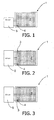
- FIG 1 shows an illumination device with an organic light-emitting diode 1 (OLED).
- OLED 1 is subdivided into an illumination area 2, where light is being emitted for an illumination purpose.
- the illumination device comprises a reference area 4 being substantially smaller than the illumination area 2.
- the illumination area 2 and the reference area 4, which are located on a same substrate, are connected separately with a driver 5.
- the driver 5 comprises a measurement circuit 6, a control circuit 7 and a fixed device characteristic 8.
- said measurement circuit 6 detects an active value of the illumination area 2 and a reference value of the reference area 4.
- the active value of the illumination area 2 will change as a function of time due to the ageing behaviour of the illumination device 1.
- the control circuit 7 compares the active and the reference value and produces a correction signal in response thereto to compensate the changes in the light output in the illumination area 2.
- the fixed device characteristic 8 calculates the correction signal for the illumination area 2 based on the values of the illumination area (2) and the reference areas (4). Before the control circuit 7 compares both detected values a conversion process of said values is started. The amount of compensation to achieve a constant light output of the illumination device is achieved by the fixed device characteristic 8, which determines a correction signal.
- the fixed device characteristic 8 can comprise a mathematic function for generating the correction signal.
- the fixed device characteristic 8 can include an algorithm with lookup -table in a microcontroller based in the control circuit 7.
- the driver 5 compares the behaviour of the reference area 4 to the behaviour of the illumination area 2, e.g. by measuring the device voltage for constant driving current.
- the driving current is varied for constant light output.
- the device characteristic 8 is integrated in the control circuit 7.
- Figure 2 shows an illumination device with almost the same characteristics described in Figure 1 .
- the OLED 1 is subdivided into an illumination area 2, an active area 3 and a reference area 4.
- the active area 3 and the illumination area 2 are both used for illumination purpose, wherein the active area 3 works as a reference for the illumination area 2.
- the active area 3 is a non-isolated area connected with the illumination area 2, wherein the reference area 4 is an isolated area 4.
- the active value of the active area will also change as a function of time due to the ageing behaviour of the illumination device 1.
- a current does not flow to the reference area 4.
- the active area 3 and the reference area 4 are located at the OLED 1 separately.
- the isolated reference area 4 and the non-isolated active area 3 are placed next to each other.
- the active area 3 and the reference area 4 have the same size.
- a conversion process of the detected active value and reference value is simplified.
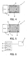
- the geometric form of the active area 3 and the reference area 4 as well as the position can be varied, which is shown in Figure 4 or Figure 5 .
- the active area 3 is located at the top side of the illumination area 2.
- the reference area 4 is placed at the opposite side (bottom side) of the illumination area 2.
- the active area 3 and the reference area 4 have the same geometric form (narrow rectangle).
- the active area 3 and the reference area 4 are a small copy (reproduction) of the illumination area 2 in order to simplify the correction calculation process.
- the illumination device can comprise more than one active area 3 and more than one reference area 4.
- two active areas 3 and two reference areas 4 are used, wherein all areas 3, 4 are located at each corner of the illumination area 2.
Abstract
Description
- The present invention relates to an illumination device comprising an organic light-emitting diode (OLED) having a light output that changes with use.
- Illumination devices with organic light-emitting diodes are of great interest as superior flat-panel systems. Theses systems utilize current passing through thin layers of organic material to generate light. The color of light emitted and the efficiency of the energy conversion from current to light are determined by the composition of the organic material. However, as the OLED is used, the organic materials in the illumination device age and become less efficient at emitting light. This reduces the lifetime of the illumination device.
-
US 2004/0070558 A1 describes an organic light-emitting diode (OLED) display system having addressable pixels on a substrate, the pixels having performance attributes, and a control circuit for controlling the pixels of the display device, comprising one or more OLED pixels and an OLED reference pixel located on a substrate and connected to the control circuit. The OLED reference pixel comprise the same performance attribute as the one or more OLED pixel, wherein the OLED reference pixel have voltage sensing circuit including a transistor connected to one of the terminals of the OLED reference pixel for sensing the voltage across the OLED reference pixel to produce a voltage signal representing the voltage across the OLED reference pixel. Furthermore, the organic light-emitting diode comprises a measurement circuit to produce an output signal representative of the performance attribute of the OLED reference pixel and an analyse circuit connected to the measurement circuit to receive the output signal, comparing the performance attributes with predetermined performance attributes, and producing a feedback signal in response thereto. The said control circuit is responsive to the feedback signal to compensate for changes in the output of the OLED pixels. Disadvantageously, the described OLED display system making use of reference pixels to compensate aging effects is restricted to displays. Large area OLED devices for illumination, however, are not pixelated. Thus, the proposed device and method inUS 2004/0070558 cannot be applied for non-pixelated illumination areas. -
US 6,081,073 andUS 6,320,325 describes the use of sensors to measure the light output. One of the essential disadvantages is that the use of additional sensors generate more costs, moreover, the degradation issue is not solved but shifted to the sensor. - The invention has for its object to eliminate the above mentioned disadvantages. In particular, it is an object of the invention to provide an illumination device, which is simple and can be easily adjusted to produce a light, whereby the light output of the illumination device is constant over its lifetime.
- This object is achieved by an illumination device as taught by claim 1 of the present invention. Accordingly, an illumination device is provided, comprising an organic light-emitting diode (OLED) having a light output that changes with use with an illumination area, where light is being emitted for an illumination purpose. Furthermore, the illumination device includes a reference area being substantially smaller than the illumination area and a substrate, on which the illumination area and the reference area are located. One of the important characteristics of the invention is that a driver is connected to the reference area and the illumination area comprising a measurement and a control circuit to drive the reference area separately to the illumination area and/or active area. The measurement circuit detects at least one active value of the illumination area and at least one reference value of the reference area. The function of the control circuit is to compare the active and the reference value and to produce a correction signal in response thereto to compensate the changes in the light outputs of the illumination area, whereby the control circuit calculates the correction signal for the illumination area based on the active value and the reference value. Thus, the illumination device comprises an illumination area, which emits light for illumination purpose being always in use during the "normal" illumination process.
Here the active area is the illumination area itself. In another embodiment the active area is an area of the illumination device, which is a reproduction of the illumination area (same layer stack), wherein the active area is always in use during the illumination process. In an embodiment the driver is connected with the illumination area, the reference area and the active area separately. The measurement circuit detects at least one active value of the illumination area and/or the active area. That means that the active area emits light during the illumination process while the illumination area is also in use. In one possible embodiment of the invention the active area is the illumination area itself. Alternatively, the active area consists of any shape substantially smaller than the illumination area. Advantageously, the active area comprises a similar shape substantially smaller than the illumination area. The reference area is an area of the illumination device, which is a reproduction of the illumination area, wherein the reference area is never in use during the illumination process. The reference area can be of any shape substantially smaller than the illumination area. Advantageously, the reference area is of similar shape substantially smaller than the illumination area. Thus, the OLED is subdivided into one or more active areas and one or more reference areas. - The OLED device of this invention is typically provided over a supporting substrate where either the cathode or anode can be in contact with the substrate. The electrode in contact with the substrate is conventionally referred to as the bottom electrode. Conventionally, the bottom electrode is the anode, but this invention is not limited to that configuration. The substrate can either be transmissive or opaque. Substrates can include, but are not limited to, glass, plastic, semiconductor materials, silicone, ceramics, circuit board materials. According to the invention the reference area is an isolated area not connected to the active area. That means that during the pure illumination process the reference area is switched-off, wherein the illumination area and/or the active area produces the light output. Only, when the control circuit is activated, the reference area is switched-on.
- Preferably, the OLED is a bottom emitting device or a top emitting device, whereby the illumination device in combination with said OLED can be used in systems with controllable color. That means that the driver compares the characteristics of both areas to determine the amount of correction for the driving of the illumination area. These values are fed into the control circuitry, which adjusts the driving current to achieve constant light output. Preferably, the driver includes a fixed device characteristic for estimating the correction signal. The fixed device characteristic can comprise a mathematic function and/or a lookup table in a microcontroller based control circuit. The compensation characteristic depends on the OLED device and can be changed programmatically. The amount of compensation to achieve a constant light output over lifetime can be realized in form of a controlling algorithm of as microcontroller based circuitry. Advantageously, the reference area, which is not fed by the driving current during the normal illumination process, can be integrated with the illumination area, which is in a preferred embodiment the active area. That means that the reference area is an integral part of the active area in a sense that both areas are located on the same substrate. The advantage is that the reference area and the active area have more or less the same characteristics especially for aging aspects.
- According to a preferred embodiment of the invention the reference area is a smaller reproduction of the illumination area. In order to compare the active and the reference value the control circuit has to convert the detected active value or the reference value in order to compare both values. For aging compensation the control circuit compares the behaviour of the reference area to the behaviour of the active area. According to one possible embodiment the active and the reference value are voltage values measured for constant driving current. Depending on the deviation of the measured values for the active area compared to the reference area the driving current is varied for constant light output. Alternatively, the active and the reference value can be a capacity value measured by the measurement circuit. The advantage for building up the reference area as a smaller reproduction of the illumination area is that for a given size of substrate the area which can be used for illumination purpose is maximized.
- According to a preferred embodiment of the invention the illumination area is the active area of the illumination device. In another possible embodiment of the illumination device the active area is a smaller reproduction of the illumination area, whereby the active area and the reference area are similar in a mathematical sense. Said active area is connected to the illumination area. Preferably, the reference area is an isolated area being not connected to the illumination area. The advantage for building up the active area as a smaller reproduction of the illumination area is that the procedure for comparing the detected values of the active and the reference area can be simplified. In this case the geometry of the reference area is almost equal to the geometry of the illumination area, wherein the reference area is scaled smaller than the illumination area. In other words, to get a good comparability, of the detected active and reference value, the dimensions of said areas are similar or equal, preferably. Surprisingly it has been found that said comparability is maximized, if reference, active and illumination area are similar in the mathematical sense, i.e. congruent to the result of a uniform scaling.
- According to another preferred embodiment the reference area and/or active area are located at the border of the illumination area. Certainly, other positions of the reference area and/or the active area are possible. The size of the reference area and/or the active area is constructed in such a way that the human eye cannot detect these areas during the illumination process of the OLED and measurement cycles for aging compensation.
- Furthermore it is preferred that more than one active area and/or reference area are positioned at the illumination area to increase the accuracy of the aging compensation and/or simplify the correction algorithm. Important is that in all described embodiment the driver is connected with the illumination area, the reference area and the active area separately.
- The isolated reference area can be made during the manufacturing process of the OLED. Alternatively, the reference area can be separated in a postproduction process, e.g. by laser cutting or placed on a separate substrate.
- The preferred invention relates to a method for controlling an aging process of an illumination device including an organic light-emitting diode (OLED) having a light output that changes with use with an illumination area and/or an active area, where light is being emitted for illumination purpose. Furthermore the illumination device comprises a reference area being substantially smaller than the illumination area, a substrate, on which the reference area and the illumination area and/or the active area are located. A driver is connected to the reference area and the illumination area and/or the active area. The inventive method comprises the steps of detecting at least one active value of the active area and at least one reference value of the reference area by a measurement circuit. After this step the active and the reference values are compared and a correction signal in response thereto to compensate the changes in the light output of the illumination area is produced by a control circuit. Said control circuit calculates the correction signal for the illumination area based on the active value and the reference value.
- The described steps of the correction calculation process may be performed continuously or periodically during use, at power-up or power-down. Alternatively, the correction calculation process may be performed in response to user signal supplied to the control circuit. The correction process can be conducted hourly, e.g. for high-precision light sources. For other lighting systems, e.g. for ambient lighting systems the intervals of the correction process can be lager. In one possible embodiment of the invention the active area is the illumination area, wherein the driver converts the detected active value or the reference value in order to compare both values. The conversion is needed because of the different sizes of the active area and the reference area.
- Alternatively, the active area has the same size as the reference area, whereby the active area is a non-isolated area connected with the illumination area. In this case the active area works as reference for the illumination area, wherein the conversion of the detected active value and the reference value is simplified. The measured values of the active area and the reference area can be different characteristics of both areas, for example voltage values or capacity values.
- According to the invention, the driver can comprise a fixed device characteristic, which determines the correction signal. The fixed device characteristic can comprise a mathematic function and/or a lookup-table to generate the correction signal. The control circuit calculates the correction signal by a special algorithm. To further reduce the possibility of complications resulting from inaccurate active and reference value readings or inadequately compensated illumination area temperatures, changes to the correction signals applied to the input signals may be limited by the control circuit. Any change in correction can be limited in magnitude, for example to a 4% change. Correction changes can also be averaged over time. Alternatively, an actual correction can be made only after taking several readings, for example every time the OLED is powered on, a correction calculation is performed and a number of calculated correction signals are averaged to produce the actual correction signal that is applied to the OLED.
- During the normal illumination process of the OLED the reference area is switched off, that means that the reference area is dark. Said reference area can be made almost invisible to the human eye by proper location in the illumination device and/or down scaling of area size of said reference area.
- The illumination device as well as the method mentioned above can be used in a variety of systems amongst them systems being automotive systems, home lighting systems, backlighting systems for displays, ambient lighting systems, flashes for cameras (with adjustable color) or shop lighting systems.
- The aforementioned components, as well as the claimed components and the components to be used in accordance with the invention in the described embodiments, are not subject to any special exceptions with respect to the size, shape, material selection as technical concept such that the selection criteria known in the pertinent field can be applied without limitations.
- Additional details, characteristics and advantages of the object of the invention are disclosed in the subclaims and the following description of the respective Figures -which is an exemplary fashion- show several preferred embodiments of the illumination device according to the invention.
-
Figure 1 shows a very schematic view of an illumination device according to a first embodiment of the present invention, -
Figure 2 shows a very schematic view of an illumination device according to a second embodiment of the present invention, -
Figure 3 shows a very schematic view of an illumination device according to a third embodiment of the present invention, -
Figure 4 shows a very schematic view of an illumination device according to a fourth embodiment of the present invention, -
Figure 5 shows a very schematic view of an illumination device according to a fifth embodiment of the present invention and -
Figure 6 shows a very schematic view of an illumination device connected with a driver. -
Figure 1 shows an illumination device with an organic light-emitting diode 1 (OLED). The OLED 1 is subdivided into anillumination area 2, where light is being emitted for an illumination purpose. Furthermore, the illumination device comprises areference area 4 being substantially smaller than theillumination area 2. Theillumination area 2 and thereference area 4, which are located on a same substrate, are connected separately with adriver 5. As shown inFigure 6 , thedriver 5 comprises ameasurement circuit 6, acontrol circuit 7 and afixed device characteristic 8. - For the correction calculation process to control the aging of the OLED said
measurement circuit 6 detects an active value of theillumination area 2 and a reference value of thereference area 4. The active value of theillumination area 2 will change as a function of time due to the ageing behaviour of the illumination device 1. Thecontrol circuit 7 compares the active and the reference value and produces a correction signal in response thereto to compensate the changes in the light output in theillumination area 2. The fixeddevice characteristic 8 calculates the correction signal for theillumination area 2 based on the values of the illumination area (2) and the reference areas (4). Before thecontrol circuit 7 compares both detected values a conversion process of said values is started. The amount of compensation to achieve a constant light output of the illumination device is achieved by the fixeddevice characteristic 8, which determines a correction signal. In a possible embodiment of the invention the fixed device characteristic 8 can comprise a mathematic function for generating the correction signal. Also the fixed device characteristic 8 can include an algorithm with lookup -table in a microcontroller based in thecontrol circuit 7. During the normal illumination process thereference area 4 is not activated, i.e. a current does not flow through thisarea 4. For aging compensation thedriver 5 compares the behaviour of thereference area 4 to the behaviour of theillumination area 2, e.g. by measuring the device voltage for constant driving current. Depending on the deviation of the measured values for theillumination area 2 compared to thereference area 4 the driving current is varied for constant light output. In another not shown embodiment thedevice characteristic 8 is integrated in thecontrol circuit 7. -
Figure 2 shows an illumination device with almost the same characteristics described inFigure 1 . One of the essential differences is that the OLED 1 is subdivided into anillumination area 2, anactive area 3 and areference area 4. Theactive area 3 and theillumination area 2 are both used for illumination purpose, wherein theactive area 3 works as a reference for theillumination area 2. Theactive area 3 is a non-isolated area connected with theillumination area 2, wherein thereference area 4 is anisolated area 4. The active value of the active area will also change as a function of time due to the ageing behaviour of the illumination device 1. During the normal operation of the OLED 1 a current does not flow to thereference area 4. Theactive area 3 and thereference area 4 are located at the OLED 1 separately. According toFigure 3 it is also possible that theisolated reference area 4 and the non-isolatedactive area 3 are placed next to each other. Advantageously, theactive area 3 and thereference area 4 have the same size. Thus, a conversion process of the detected active value and reference value is simplified. - Certainly, the geometric form of the
active area 3 and thereference area 4 as well as the position can be varied, which is shown inFigure 4 or Figure 5 . According toFigure 4 theactive area 3 is located at the top side of theillumination area 2. Thereference area 4 is placed at the opposite side (bottom side) of theillumination area 2. In the shown embodiment ofFigure 4 theactive area 3 and thereference area 4 have the same geometric form (narrow rectangle). In the described embodiments ofFigure 2-5 theactive area 3 and thereference area 4 are a small copy (reproduction) of theillumination area 2 in order to simplify the correction calculation process. As illustrated inFigure 5 , the illumination device can comprise more than oneactive area 3 and more than onereference area 4. In this embodiment twoactive areas 3 and tworeference areas 4 are used, wherein allareas illumination area 2. -
- 1
- light-emitting diode (OLED)
- 2
- illumination area
- 3
- active area
- 4
- reference area
- 5
- driver
- 6
- measurement circuit
- 7
- control circuit
- 8
- fixed device characteristic
Claims (12)
- An illumination device representing an electrical property comprisinga) an organic light-emitting diode having a light output that changes with use, the organic light-emitting diode being subdivided into an illumination area (2), where light is being emitted for an illumination purpose, and a reference area (4) being substantially smaller than the illumination area (2), wherein the reference area (4) is an electrically isolated area (4) not connected to the illumination area (2),b) a substrate, on which the reference area (4) and the illumination area (2) are located,c) a driver (5) connected to the reference area (4) and the illumination area (2) to drive the reference area (4) separately from the illumination area (2), with
a measurement circuit (6) detecting at least one active value representing an electrical property of the illumination area (2) and at least one reference value representing an electrical property of the reference area (4), preferably the active values and the reference values are voltage values measured for constant driving current or are capacity values,
a control circuit (7), which compares the active and the reference values and produces a correction signal in response thereto to compensate for the changes in the light output of the illumination area (2), wherein
the control circuit (7) calculates the correction signal for the illumination area (2) based on the active value and the reference value. - Illumination device as claimed in claim 1, characterized in that the substrate further comprises an active area (3) emitting light during the illumination process, which is substantially smaller than the illumination area (2) and being a reproduction of the illumination area (2).
- Illumination device as claimed in claim 2, characterized in that the driver (5) is connected to the illumination area (2), the reference area (4) and the active area (3) separately.
- Illumination device according to claims 2 or 3, characterized in that the measurement circuit (6) detects at least one active value of the illumination area (2) and the active area (3).
- Illumination device according to any preceding claims, characterized in that the reference area (4) is located at the border of the illumination area (2).
- Illumination device according to any preceding claims, characterized in that the driver (5) includes a fixed device characteristic (8) for estimating the correction signal.
- A method for controlling an aging process of an illumination device including an organic light-emitting diode (1) according to claim 1 comprising the steps of:detecting the at least one active value of the illumination area (2) an the at least one reference value of the reference area (4) by the measurement circuit (6),comparing the active and the reference value and producing the correction signal in response thereto to compensate the changes in the light output of the illumination area (2) by the control circuit (7), which calculates the correction signal for the illumination area (2) based on the active value and the reference value.
- The method as claimed in claim 7, characterized in that a fixed device characteristic (8) determines the correction signal.
- The method as claimed in claim 8, characterized in that the fixed device characteristic (8) comprises a mathematic function and/or a lookup table to generate the correction signal.
- The method according to any of claims 7 to 9, characterized in that the steps of claim 8 are conducted periodically, wherein for normal illumination of the illumination device (1) the reference area (4) is switched off.
- The method according to any of claims 7 to 10, characterized in that the active and the reference value are current values and/or voltage values and/or capacity values.
- The method according to any of claims 7 to 11, where the substrate of the illumination device further comprises an active area (3) emitting light during the illumination process, which is substantially smaller than the illumination area (2) and being a reproduction of the illumination area (2) and that the driver (5) is connected with the illumination area (2), the reference area (4) and the active area (3) separately, comprising the step of detecting at least one active value of the illumination area (2) and the active area (3).
Priority Applications (1)
| Application Number | Priority Date | Filing Date | Title |
|---|---|---|---|
| EP06809556A EP1941484B1 (en) | 2005-10-20 | 2006-10-10 | Illumination device |
Applications Claiming Priority (3)
| Application Number | Priority Date | Filing Date | Title |
|---|---|---|---|
| EP05109792 | 2005-10-20 | ||
| EP06809556A EP1941484B1 (en) | 2005-10-20 | 2006-10-10 | Illumination device |
| PCT/IB2006/053716 WO2007046030A1 (en) | 2005-10-20 | 2006-10-10 | Illumination device |
Publications (2)
| Publication Number | Publication Date |
|---|---|
| EP1941484A1 EP1941484A1 (en) | 2008-07-09 |
| EP1941484B1 true EP1941484B1 (en) | 2011-12-21 |
Family
ID=37770433
Family Applications (1)
| Application Number | Title | Priority Date | Filing Date |
|---|---|---|---|
| EP06809556A Not-in-force EP1941484B1 (en) | 2005-10-20 | 2006-10-10 | Illumination device |
Country Status (8)
| Country | Link |
|---|---|
| US (1) | US7538306B2 (en) |
| EP (1) | EP1941484B1 (en) |
| JP (1) | JP5118050B2 (en) |
| KR (1) | KR101315088B1 (en) |
| CN (1) | CN101292276B (en) |
| AT (1) | ATE538467T1 (en) |
| TW (1) | TW200729136A (en) |
| WO (1) | WO2007046030A1 (en) |
Families Citing this family (12)
| Publication number | Priority date | Publication date | Assignee | Title |
|---|---|---|---|---|
| TW200950178A (en) * | 2008-01-30 | 2009-12-01 | Koninkl Philips Electronics Nv | OLED lighting device |
| TWI398839B (en) * | 2009-05-27 | 2013-06-11 | Univ Nat Taipei Technology | Auto-compensating system for a surface light source of an organic light-emitting diodes |
| US8339386B2 (en) * | 2009-09-29 | 2012-12-25 | Global Oled Technology Llc | Electroluminescent device aging compensation with reference subpixels |
| JP2011243894A (en) * | 2010-05-21 | 2011-12-01 | Sanken Electric Co Ltd | Organic el lighting device |
| KR20120022411A (en) * | 2010-09-02 | 2012-03-12 | 삼성모바일디스플레이주식회사 | Display device and driving method thereof |
| KR101991029B1 (en) * | 2012-08-16 | 2019-06-19 | 엘지이노텍 주식회사 | System for controlling lighting device |
| JP6091166B2 (en) * | 2012-11-08 | 2017-03-08 | 株式会社カネカ | Organic EL device |
| KR102260443B1 (en) * | 2014-10-06 | 2021-06-07 | 삼성디스플레이 주식회사 | Display device and driving method of the same |
| KR102227636B1 (en) * | 2014-12-31 | 2021-03-16 | 삼성디스플레이 주식회사 | Data storage device for display device and method of storaging data thereof |
| EP3076757B1 (en) | 2015-03-30 | 2023-01-04 | OLEDWorks GmbH | Oled device and driving method |
| CN105280139B (en) * | 2015-11-11 | 2018-05-01 | 深圳市华星光电技术有限公司 | AMOLED luminance compensation methods and AMOLED drive systems |
| CN110808006B (en) * | 2019-09-06 | 2021-01-15 | 华为技术有限公司 | Display screen aging compensation method, circuit system and electronic equipment |
Family Cites Families (10)
| Publication number | Priority date | Publication date | Assignee | Title |
|---|---|---|---|---|
| US6081073A (en) | 1995-12-19 | 2000-06-27 | Unisplay S.A. | Matrix display with matched solid-state pixels |
| EP1158483A3 (en) | 2000-05-24 | 2003-02-05 | Eastman Kodak Company | Solid-state display with reference pixel |
| JP2002162934A (en) * | 2000-09-29 | 2002-06-07 | Eastman Kodak Co | Flat-panel display with luminance feedback |
| US6320325B1 (en) * | 2000-11-06 | 2001-11-20 | Eastman Kodak Company | Emissive display with luminance feedback from a representative pixel |
| JP2002304155A (en) * | 2001-01-29 | 2002-10-18 | Semiconductor Energy Lab Co Ltd | Light-emitting device |
| US20020171611A1 (en) * | 2001-05-15 | 2002-11-21 | Eastman Kodak Company | Active matrix organic light emitting diode flat-panel display |
| JP2003043998A (en) * | 2001-07-30 | 2003-02-14 | Pioneer Electronic Corp | Display device |
| US7274363B2 (en) * | 2001-12-28 | 2007-09-25 | Pioneer Corporation | Panel display driving device and driving method |
| WO2004086345A1 (en) | 2003-03-27 | 2004-10-07 | Sanyo Electric Co., Ltd. | Display irregularity correction method |
| WO2005081810A2 (en) * | 2004-02-24 | 2005-09-09 | Nuelight Corporation | Penlight and touch screen data input system and method for flat panel displays |
-
2006
- 2006-10-10 JP JP2008536166A patent/JP5118050B2/en not_active Expired - Fee Related
- 2006-10-10 KR KR1020087011943A patent/KR101315088B1/en not_active IP Right Cessation
- 2006-10-10 CN CN2006800389386A patent/CN101292276B/en not_active Expired - Fee Related
- 2006-10-10 EP EP06809556A patent/EP1941484B1/en not_active Not-in-force
- 2006-10-10 WO PCT/IB2006/053716 patent/WO2007046030A1/en active Application Filing
- 2006-10-10 US US12/090,876 patent/US7538306B2/en not_active Expired - Fee Related
- 2006-10-10 AT AT06809556T patent/ATE538467T1/en active
- 2006-10-17 TW TW095138264A patent/TW200729136A/en unknown
Also Published As
| Publication number | Publication date |
|---|---|
| CN101292276A (en) | 2008-10-22 |
| US20080210847A1 (en) | 2008-09-04 |
| JP2009513012A (en) | 2009-03-26 |
| KR20080064871A (en) | 2008-07-09 |
| CN101292276B (en) | 2010-12-01 |
| US7538306B2 (en) | 2009-05-26 |
| ATE538467T1 (en) | 2012-01-15 |
| TW200729136A (en) | 2007-08-01 |
| WO2007046030A1 (en) | 2007-04-26 |
| EP1941484A1 (en) | 2008-07-09 |
| KR101315088B1 (en) | 2013-10-07 |
| JP5118050B2 (en) | 2013-01-16 |
Similar Documents
| Publication | Publication Date | Title |
|---|---|---|
| EP1941484B1 (en) | Illumination device | |
| EP1932137B1 (en) | A method of compensating an aging process of an illumination device | |
| US10380944B2 (en) | Structural and low-frequency non-uniformity compensation | |
| JP5071834B2 (en) | Lighting device and adjustment method | |
| US6320325B1 (en) | Emissive display with luminance feedback from a representative pixel | |
| TW582184B (en) | Organic electroluminescence device and method for driving same | |
| US20090267523A1 (en) | Driver circuit for light sheet module with direct connection to power source | |
| KR20020025785A (en) | A flat-panel display with luminance feedback | |
| JP5355904B2 (en) | Lighting device | |
| US20110284721A1 (en) | Organic electroluminescence illumination device | |
| JP2007173088A (en) | Organic electroluminescent panel and organic el lighting system using the same | |
| US20190318691A1 (en) | Structural and low-frequency non-uniformity compensation | |
| JP5138387B2 (en) | Lighting device | |
| US7081720B2 (en) | Driver circuit and method for driving electroluminescent lamp to emit light at brightness set level | |
| JP2012084370A (en) | Lighting system | |
| JP2002278506A (en) | Light emission device provided with emission luminance adjusting means, and display device using the emission device | |
| US7919935B2 (en) | Brightness sensor | |
| JP2008191539A (en) | Driving device of organic el element, and driving method of organic el element | |
| JP4893537B2 (en) | Light emitting module and manufacturing method thereof | |
| CN216161766U (en) | Electroluminescent device and display device | |
| KR102148468B1 (en) | Driving modules for oled lighting apparatus | |
| TW567353B (en) | Contrast-adjustable panels and displays via light-emitting devices | |
| TW200939888A (en) | A feedback-controlled method of LED luminance and circuit thereof | |
| KR20020095349A (en) | Calibration circuit of flat panel display device |
Legal Events
| Date | Code | Title | Description |
|---|---|---|---|
| PUAI | Public reference made under article 153(3) epc to a published international application that has entered the european phase |
Free format text: ORIGINAL CODE: 0009012 |
|
| 17P | Request for examination filed |
Effective date: 20080520 |
|
| AK | Designated contracting states |
Kind code of ref document: A1 Designated state(s): AT BE BG CH CY CZ DE DK EE ES FI FR GB GR HU IE IS IT LI LT LU LV MC NL PL PT RO SE SI SK TR |
|
| 17Q | First examination report despatched |
Effective date: 20090729 |
|
| GRAP | Despatch of communication of intention to grant a patent |
Free format text: ORIGINAL CODE: EPIDOSNIGR1 |
|
| DAX | Request for extension of the european patent (deleted) | ||
| RIN1 | Information on inventor provided before grant (corrected) |
Inventor name: HENTE, DIRK Inventor name: YOUNG, EDWARD WILLEM ALBERT |
|
| GRAS | Grant fee paid |
Free format text: ORIGINAL CODE: EPIDOSNIGR3 |
|
| GRAA | (expected) grant |
Free format text: ORIGINAL CODE: 0009210 |
|
| AK | Designated contracting states |
Kind code of ref document: B1 Designated state(s): AT BE BG CH CY CZ DE DK EE ES FI FR GB GR HU IE IS IT LI LT LU LV MC NL PL PT RO SE SI SK TR |
|
| REG | Reference to a national code |
Ref country code: GB Ref legal event code: FG4D |
|
| REG | Reference to a national code |
Ref country code: CH Ref legal event code: EP |
|
| REG | Reference to a national code |
Ref country code: AT Ref legal event code: REF Ref document number: 538467 Country of ref document: AT Kind code of ref document: T Effective date: 20120115 |
|
| REG | Reference to a national code |
Ref country code: IE Ref legal event code: FG4D |
|
| REG | Reference to a national code |
Ref country code: DE Ref legal event code: R096 Ref document number: 602006026598 Country of ref document: DE Effective date: 20120223 |
|
| REG | Reference to a national code |
Ref country code: NL Ref legal event code: VDEP Effective date: 20111221 |
|
| PG25 | Lapsed in a contracting state [announced via postgrant information from national office to epo] |
Ref country code: LT Free format text: LAPSE BECAUSE OF FAILURE TO SUBMIT A TRANSLATION OF THE DESCRIPTION OR TO PAY THE FEE WITHIN THE PRESCRIBED TIME-LIMIT Effective date: 20111221 |
|
| LTIE | Lt: invalidation of european patent or patent extension |
Effective date: 20111221 |
|
| PG25 | Lapsed in a contracting state [announced via postgrant information from national office to epo] |
Ref country code: SE Free format text: LAPSE BECAUSE OF FAILURE TO SUBMIT A TRANSLATION OF THE DESCRIPTION OR TO PAY THE FEE WITHIN THE PRESCRIBED TIME-LIMIT Effective date: 20111221 Ref country code: GR Free format text: LAPSE BECAUSE OF FAILURE TO SUBMIT A TRANSLATION OF THE DESCRIPTION OR TO PAY THE FEE WITHIN THE PRESCRIBED TIME-LIMIT Effective date: 20120322 Ref country code: LV Free format text: LAPSE BECAUSE OF FAILURE TO SUBMIT A TRANSLATION OF THE DESCRIPTION OR TO PAY THE FEE WITHIN THE PRESCRIBED TIME-LIMIT Effective date: 20111221 Ref country code: NL Free format text: LAPSE BECAUSE OF FAILURE TO SUBMIT A TRANSLATION OF THE DESCRIPTION OR TO PAY THE FEE WITHIN THE PRESCRIBED TIME-LIMIT Effective date: 20111221 Ref country code: SI Free format text: LAPSE BECAUSE OF FAILURE TO SUBMIT A TRANSLATION OF THE DESCRIPTION OR TO PAY THE FEE WITHIN THE PRESCRIBED TIME-LIMIT Effective date: 20111221 |
|
| PG25 | Lapsed in a contracting state [announced via postgrant information from national office to epo] |
Ref country code: CY Free format text: LAPSE BECAUSE OF FAILURE TO SUBMIT A TRANSLATION OF THE DESCRIPTION OR TO PAY THE FEE WITHIN THE PRESCRIBED TIME-LIMIT Effective date: 20111221 Ref country code: BE Free format text: LAPSE BECAUSE OF FAILURE TO SUBMIT A TRANSLATION OF THE DESCRIPTION OR TO PAY THE FEE WITHIN THE PRESCRIBED TIME-LIMIT Effective date: 20111221 |
|
| PG25 | Lapsed in a contracting state [announced via postgrant information from national office to epo] |
Ref country code: IS Free format text: LAPSE BECAUSE OF FAILURE TO SUBMIT A TRANSLATION OF THE DESCRIPTION OR TO PAY THE FEE WITHIN THE PRESCRIBED TIME-LIMIT Effective date: 20120421 Ref country code: SK Free format text: LAPSE BECAUSE OF FAILURE TO SUBMIT A TRANSLATION OF THE DESCRIPTION OR TO PAY THE FEE WITHIN THE PRESCRIBED TIME-LIMIT Effective date: 20111221 Ref country code: CZ Free format text: LAPSE BECAUSE OF FAILURE TO SUBMIT A TRANSLATION OF THE DESCRIPTION OR TO PAY THE FEE WITHIN THE PRESCRIBED TIME-LIMIT Effective date: 20111221 Ref country code: EE Free format text: LAPSE BECAUSE OF FAILURE TO SUBMIT A TRANSLATION OF THE DESCRIPTION OR TO PAY THE FEE WITHIN THE PRESCRIBED TIME-LIMIT Effective date: 20111221 Ref country code: BG Free format text: LAPSE BECAUSE OF FAILURE TO SUBMIT A TRANSLATION OF THE DESCRIPTION OR TO PAY THE FEE WITHIN THE PRESCRIBED TIME-LIMIT Effective date: 20120321 |
|
| PG25 | Lapsed in a contracting state [announced via postgrant information from national office to epo] |
Ref country code: PL Free format text: LAPSE BECAUSE OF FAILURE TO SUBMIT A TRANSLATION OF THE DESCRIPTION OR TO PAY THE FEE WITHIN THE PRESCRIBED TIME-LIMIT Effective date: 20111221 Ref country code: RO Free format text: LAPSE BECAUSE OF FAILURE TO SUBMIT A TRANSLATION OF THE DESCRIPTION OR TO PAY THE FEE WITHIN THE PRESCRIBED TIME-LIMIT Effective date: 20111221 Ref country code: PT Free format text: LAPSE BECAUSE OF FAILURE TO SUBMIT A TRANSLATION OF THE DESCRIPTION OR TO PAY THE FEE WITHIN THE PRESCRIBED TIME-LIMIT Effective date: 20120423 |
|
| REG | Reference to a national code |
Ref country code: AT Ref legal event code: MK05 Ref document number: 538467 Country of ref document: AT Kind code of ref document: T Effective date: 20111221 |
|
| PLBE | No opposition filed within time limit |
Free format text: ORIGINAL CODE: 0009261 |
|
| STAA | Information on the status of an ep patent application or granted ep patent |
Free format text: STATUS: NO OPPOSITION FILED WITHIN TIME LIMIT |
|
| PG25 | Lapsed in a contracting state [announced via postgrant information from national office to epo] |
Ref country code: DK Free format text: LAPSE BECAUSE OF FAILURE TO SUBMIT A TRANSLATION OF THE DESCRIPTION OR TO PAY THE FEE WITHIN THE PRESCRIBED TIME-LIMIT Effective date: 20111221 |
|
| 26N | No opposition filed |
Effective date: 20120924 |
|
| PG25 | Lapsed in a contracting state [announced via postgrant information from national office to epo] |
Ref country code: IT Free format text: LAPSE BECAUSE OF FAILURE TO SUBMIT A TRANSLATION OF THE DESCRIPTION OR TO PAY THE FEE WITHIN THE PRESCRIBED TIME-LIMIT Effective date: 20111221 |
|
| REG | Reference to a national code |
Ref country code: DE Ref legal event code: R097 Ref document number: 602006026598 Country of ref document: DE Effective date: 20120924 |
|
| PG25 | Lapsed in a contracting state [announced via postgrant information from national office to epo] |
Ref country code: AT Free format text: LAPSE BECAUSE OF FAILURE TO SUBMIT A TRANSLATION OF THE DESCRIPTION OR TO PAY THE FEE WITHIN THE PRESCRIBED TIME-LIMIT Effective date: 20111221 |
|
| PG25 | Lapsed in a contracting state [announced via postgrant information from national office to epo] |
Ref country code: ES Free format text: LAPSE BECAUSE OF FAILURE TO SUBMIT A TRANSLATION OF THE DESCRIPTION OR TO PAY THE FEE WITHIN THE PRESCRIBED TIME-LIMIT Effective date: 20120401 |
|
| PG25 | Lapsed in a contracting state [announced via postgrant information from national office to epo] |
Ref country code: MC Free format text: LAPSE BECAUSE OF NON-PAYMENT OF DUE FEES Effective date: 20121031 |
|
| REG | Reference to a national code |
Ref country code: CH Ref legal event code: PL |
|
| PG25 | Lapsed in a contracting state [announced via postgrant information from national office to epo] |
Ref country code: FI Free format text: LAPSE BECAUSE OF FAILURE TO SUBMIT A TRANSLATION OF THE DESCRIPTION OR TO PAY THE FEE WITHIN THE PRESCRIBED TIME-LIMIT Effective date: 20111221 |
|
| REG | Reference to a national code |
Ref country code: IE Ref legal event code: MM4A |
|
| PG25 | Lapsed in a contracting state [announced via postgrant information from national office to epo] |
Ref country code: IE Free format text: LAPSE BECAUSE OF NON-PAYMENT OF DUE FEES Effective date: 20121010 Ref country code: CH Free format text: LAPSE BECAUSE OF NON-PAYMENT OF DUE FEES Effective date: 20121031 Ref country code: LI Free format text: LAPSE BECAUSE OF NON-PAYMENT OF DUE FEES Effective date: 20121031 |
|
| PG25 | Lapsed in a contracting state [announced via postgrant information from national office to epo] |
Ref country code: TR Free format text: LAPSE BECAUSE OF FAILURE TO SUBMIT A TRANSLATION OF THE DESCRIPTION OR TO PAY THE FEE WITHIN THE PRESCRIBED TIME-LIMIT Effective date: 20111221 |
|
| REG | Reference to a national code |
Ref country code: DE Ref legal event code: R081 Ref document number: 602006026598 Country of ref document: DE Owner name: PHILIPS GMBH, DE Free format text: FORMER OWNER: PHILIPS INTELLECTUAL PROPERTY & STANDARDS GMBH, 20099 HAMBURG, DE Effective date: 20140327 Ref country code: DE Ref legal event code: R081 Ref document number: 602006026598 Country of ref document: DE Owner name: OLEDWORKS GMBH, DE Free format text: FORMER OWNER: PHILIPS INTELLECTUAL PROPERTY & STANDARDS GMBH, 20099 HAMBURG, DE Effective date: 20140327 Ref country code: DE Ref legal event code: R081 Ref document number: 602006026598 Country of ref document: DE Owner name: PHILIPS DEUTSCHLAND GMBH, DE Free format text: FORMER OWNER: PHILIPS INTELLECTUAL PROPERTY & STANDARDS GMBH, 20099 HAMBURG, DE Effective date: 20140327 |
|
| PG25 | Lapsed in a contracting state [announced via postgrant information from national office to epo] |
Ref country code: LU Free format text: LAPSE BECAUSE OF NON-PAYMENT OF DUE FEES Effective date: 20121010 |
|
| PG25 | Lapsed in a contracting state [announced via postgrant information from national office to epo] |
Ref country code: HU Free format text: LAPSE BECAUSE OF FAILURE TO SUBMIT A TRANSLATION OF THE DESCRIPTION OR TO PAY THE FEE WITHIN THE PRESCRIBED TIME-LIMIT Effective date: 20061010 |
|
| REG | Reference to a national code |
Ref country code: FR Ref legal event code: CD Owner name: PHILIPS INTELLECTUAL PROPERTY & STANDARDS GMBH, DE Effective date: 20141126 Ref country code: FR Ref legal event code: CD Owner name: KONINKLIJKE PHILIPS ELECTRONICS N.V., NL Effective date: 20141126 Ref country code: FR Ref legal event code: CA Effective date: 20141126 |
|
| REG | Reference to a national code |
Ref country code: DE Ref legal event code: R082 Ref document number: 602006026598 Country of ref document: DE Representative=s name: MEISSNER, BOLTE & PARTNER GBR, DE Ref country code: DE Ref legal event code: R081 Ref document number: 602006026598 Country of ref document: DE Owner name: PHILIPS GMBH, DE Free format text: FORMER OWNER: PHILIPS DEUTSCHLAND GMBH, 20099 HAMBURG, DE Ref country code: DE Ref legal event code: R082 Ref document number: 602006026598 Country of ref document: DE Representative=s name: JOSTARNDT PATENTANWALTS-AG, DE Ref country code: DE Ref legal event code: R081 Ref document number: 602006026598 Country of ref document: DE Owner name: OLEDWORKS GMBH, DE Free format text: FORMER OWNER: PHILIPS DEUTSCHLAND GMBH, 20099 HAMBURG, DE |
|
| REG | Reference to a national code |
Ref country code: FR Ref legal event code: PLFP Year of fee payment: 10 |
|
| REG | Reference to a national code |
Ref country code: DE Ref legal event code: R082 Ref document number: 602006026598 Country of ref document: DE Representative=s name: JOSTARNDT PATENTANWALTS-AG, DE |
|
| REG | Reference to a national code |
Ref country code: GB Ref legal event code: 732E Free format text: REGISTERED BETWEEN 20160128 AND 20160203 |
|
| REG | Reference to a national code |
Ref country code: DE Ref legal event code: R082 Ref document number: 602006026598 Country of ref document: DE Representative=s name: JOSTARNDT PATENTANWALTS-AG, DE Ref country code: DE Ref legal event code: R081 Ref document number: 602006026598 Country of ref document: DE Owner name: OLEDWORKS GMBH, DE Free format text: FORMER OWNER: PHILIPS GMBH, 20099 HAMBURG, DE |
|
| REG | Reference to a national code |
Ref country code: FR Ref legal event code: TP Owner name: OLEDWORKS GMBH, DE Effective date: 20160405 |
|
| REG | Reference to a national code |
Ref country code: FR Ref legal event code: PLFP Year of fee payment: 11 |
|
| PGFP | Annual fee paid to national office [announced via postgrant information from national office to epo] |
Ref country code: FR Payment date: 20160919 Year of fee payment: 11 |
|
| PGFP | Annual fee paid to national office [announced via postgrant information from national office to epo] |
Ref country code: DE Payment date: 20161004 Year of fee payment: 11 Ref country code: GB Payment date: 20161005 Year of fee payment: 11 |
|
| REG | Reference to a national code |
Ref country code: DE Ref legal event code: R119 Ref document number: 602006026598 Country of ref document: DE |
|
| GBPC | Gb: european patent ceased through non-payment of renewal fee |
Effective date: 20171010 |
|
| REG | Reference to a national code |
Ref country code: FR Ref legal event code: ST Effective date: 20180629 |
|
| PG25 | Lapsed in a contracting state [announced via postgrant information from national office to epo] |
Ref country code: DE Free format text: LAPSE BECAUSE OF NON-PAYMENT OF DUE FEES Effective date: 20180501 Ref country code: GB Free format text: LAPSE BECAUSE OF NON-PAYMENT OF DUE FEES Effective date: 20171010 |
|
| PG25 | Lapsed in a contracting state [announced via postgrant information from national office to epo] |
Ref country code: FR Free format text: LAPSE BECAUSE OF NON-PAYMENT OF DUE FEES Effective date: 20171031 |