EP1973197A1 - Multi-band slot-strip antenna - Google Patents
Multi-band slot-strip antenna Download PDFInfo
- Publication number
- EP1973197A1 EP1973197A1 EP07104442A EP07104442A EP1973197A1 EP 1973197 A1 EP1973197 A1 EP 1973197A1 EP 07104442 A EP07104442 A EP 07104442A EP 07104442 A EP07104442 A EP 07104442A EP 1973197 A1 EP1973197 A1 EP 1973197A1
- Authority
- EP
- European Patent Office
- Prior art keywords
- slot
- strip
- strip structure
- band
- conductive region
- Prior art date
- Legal status (The legal status is an assumption and is not a legal conclusion. Google has not performed a legal analysis and makes no representation as to the accuracy of the status listed.)
- Granted
Links
Images


Classifications
-
- H—ELECTRICITY
- H01—ELECTRIC ELEMENTS
- H01Q—ANTENNAS, i.e. RADIO AERIALS
- H01Q9/00—Electrically-short antennas having dimensions not more than twice the operating wavelength and consisting of conductive active radiating elements
- H01Q9/04—Resonant antennas
- H01Q9/0407—Substantially flat resonant element parallel to ground plane, e.g. patch antenna
- H01Q9/0421—Substantially flat resonant element parallel to ground plane, e.g. patch antenna with a shorting wall or a shorting pin at one end of the element
-
- H—ELECTRICITY
- H01—ELECTRIC ELEMENTS
- H01Q—ANTENNAS, i.e. RADIO AERIALS
- H01Q1/00—Details of, or arrangements associated with, antennas
- H01Q1/12—Supports; Mounting means
- H01Q1/22—Supports; Mounting means by structural association with other equipment or articles
- H01Q1/24—Supports; Mounting means by structural association with other equipment or articles with receiving set
- H01Q1/241—Supports; Mounting means by structural association with other equipment or articles with receiving set used in mobile communications, e.g. GSM
- H01Q1/242—Supports; Mounting means by structural association with other equipment or articles with receiving set used in mobile communications, e.g. GSM specially adapted for hand-held use
- H01Q1/243—Supports; Mounting means by structural association with other equipment or articles with receiving set used in mobile communications, e.g. GSM specially adapted for hand-held use with built-in antennas
-
- H—ELECTRICITY
- H01—ELECTRIC ELEMENTS
- H01Q—ANTENNAS, i.e. RADIO AERIALS
- H01Q1/00—Details of, or arrangements associated with, antennas
- H01Q1/36—Structural form of radiating elements, e.g. cone, spiral, umbrella; Particular materials used therewith
- H01Q1/38—Structural form of radiating elements, e.g. cone, spiral, umbrella; Particular materials used therewith formed by a conductive layer on an insulating support
-
- H—ELECTRICITY
- H01—ELECTRIC ELEMENTS
- H01Q—ANTENNAS, i.e. RADIO AERIALS
- H01Q13/00—Waveguide horns or mouths; Slot antennas; Leaky-waveguide antennas; Equivalent structures causing radiation along the transmission path of a guided wave
- H01Q13/10—Resonant slot antennas
-
- H—ELECTRICITY
- H01—ELECTRIC ELEMENTS
- H01Q—ANTENNAS, i.e. RADIO AERIALS
- H01Q5/00—Arrangements for simultaneous operation of antennas on two or more different wavebands, e.g. dual-band or multi-band arrangements
- H01Q5/30—Arrangements for providing operation on different wavebands
- H01Q5/307—Individual or coupled radiating elements, each element being fed in an unspecified way
- H01Q5/342—Individual or coupled radiating elements, each element being fed in an unspecified way for different propagation modes
- H01Q5/357—Individual or coupled radiating elements, each element being fed in an unspecified way for different propagation modes using a single feed point
- H01Q5/364—Creating multiple current paths
- H01Q5/371—Branching current paths
-
- H—ELECTRICITY
- H01—ELECTRIC ELEMENTS
- H01Q—ANTENNAS, i.e. RADIO AERIALS
- H01Q5/00—Arrangements for simultaneous operation of antennas on two or more different wavebands, e.g. dual-band or multi-band arrangements
- H01Q5/30—Arrangements for providing operation on different wavebands
- H01Q5/378—Combination of fed elements with parasitic elements
- H01Q5/385—Two or more parasitic elements
Definitions
- the invention described herein relates generally to a multi-band antenna for a handheld wireless communications device.
- the invention relates to a multi-band slot-strip antenna.
- Slot antennas typically comprise a slot cut into a metal sheet or printed circuit board. Since some modem communication devices are required to operate in multiple frequency bands, multi-band slot antennas have been developed for use in such devices.
- Chang US 7,006,048 describes a dual-band slot antenna for satellite and/or RFID communication systems.
- the slot antenna comprises two interconnected L-shaped slot antenna structures, and a printed circuit feed line that is coupled to both of the L-shaped slot antenna structures.
- Sun US 6,677,909 describes dual-band slot antenna that comprises a pair of meandering slots, and a coaxial feed cable that is connected to the meandering slots.
- Planar inverted-F antennas are becoming increasingly common in wireless handheld communication devices due to their reduced size in comparison to conventional microstrip antenna designs. Therefore, PIFA antennas have been developed which include multiple resonant sections, each having a respective resonant frequency.
- broadband technologies such as parasitic elements and/or multi-layer structures, have been used to modify the conventional PIFA antenna for multi-band and broadband applications.
- a multi-band antenna may comprise at least three slot-strip structures configured with multiple ground pins.
- a multi-band slot-strip antenna that comprises a planar conductive layer comprising a conductive region and a non-conductive region.
- the conductive region and the non-conductive region together may define a first slot-strip structure, a second slot-strip structure coupled to the first slot-strip structure, and a third slot-strip structure coupled to the second slot-strip structure.
- the first slot-strip structure may comprise a signal feed portion.
- the second slot-strip structure may include a first signal grounding portion.
- the third slot-strip structure comprises a second signal grounding portion.
- a wireless communication device that comprises a radio transceiver section, and a multi-band slot-strip antenna coupled to the radio transceiver section.
- the multi-band slot-strip antenna may comprise a planar conductive layer comprising a conductive region and a non-conductive region. The conductive region and the non-conductive region together may define a first slot-strip structure, a second slot-strip structure coupled to the first slot-strip structure, and a third slot-strip structure coupled to the second slot-strip structure.
- the first slot-strip structure may comprise a signal feed portion.
- the second slot-strip structure may include a first signal grounding portion.
- the third slot-strip structure may comprise a second signal grounding portion. The signal feed portion may be coupled to the radio transceiver section.
- a multi-band slot-strip antenna that comprises a planar conductive layer comprising a conductive region and a non-conductive region.
- the conductive region and the non-conductive region together may define a plurality of mutually-coupled slot-strip structures.
- the slot-strip antenna also may comprise a feed signal pin connected to one of the slot-strip structures, and a ground pin connected to the other slot-strip structures.
- the multi-band antenna offers enhanced low frequency bandwidth around 2 GHz for 3G communications, from a structure whose size is suitable for incorporation into small handheld communications devices.
- the handheld communications device 200 is a two-way wireless communications device having at least voice and data communication capabilities, and is configured to operate within a wireless cellular network.
- the wireless handheld communications device 200 may be referred to as a data messaging device, a two-way pager, a wireless e-mail device, a cellular telephone with data messaging capabilities, a wireless Internet appliance, or a data communication device, as examples.
- the handheld communications device 200 includes a display 222, a function key 246, and data processing means (not shown) disposed within a common housing 201.
- the display 222 comprises a backlit LCD display.
- the data processing means is in communication with the display 222 and the function key 246.
- the backlit display 222 comprises a transmissive LCD display, and the function key 246 operates as a power on/off switch.
- the backlit display 222 comprises a reflective or trans-reflective LCD display, and the function key 246 operates as a backlight switch.
- the handheld communications device 200 includes user data input means for inputting data to the data processing means.
- the user data input means includes a keyboard 232, a thumbwheel 248 and an escape key 260.
- the keyboard 232 includes alphabetic and numerical keys, and preferably also includes a "Send” key and an "End” key to respectively initiate and terminate voice communication.
- the data input means is not limited to these forms of data input.
- the data input means may include a trackball or other pointing device instead of (or in addition to) the thumbwheel 248.
- Fig. 2 depicts functional details of the handheld communications device 200.
- the handheld communications device 200 incorporates a motherboard that includes a communication subsystem 211, and a microprocessor 238.
- the communication subsystem 211 performs communication functions, such as data and voice communications, and includes a primary transmitter/receiver 212, a secondary transmitter/receiver 214, a primary internal antenna 216 for the primary transmitter/receiver 212, a secondary internal antenna 300 for the secondary transmitter/receiver 214, and local oscillators (LOs) 213 and one or more digital signal processors (DSP) 220 coupled to the transmitter/receivers 212, 214.
- LOs local oscillators
- DSP digital signal processors
- the communication subsystem 211 sends and receives wireless communication signals over a wireless cellular network via the primary transmitter/receiver 212 and the primary internal antenna 216. Further, typically the communication subsystem 211 sends and receives wireless communication signals over a local area wireless network via the secondary transmitter/receiver 214 and the secondary internal antenna 300.
- the primary internal antenna 216 is configured for use within a Global System for Mobile Communications (GSM) cellular network or a Code Division Multiple Access (CDMA) cellular network.
- the secondary internal antenna 300 is configured for use within a Universal Mobile Telecommunications Service (UMTS) or WLAN WiFi (IEEE 802.1 1x) network. More preferably, the secondary internal antenna 300 is a multi-band slot-strip antenna that is configured for use with networks whose operational frequencies are at/near 2GHz and 5 GHz, and whose low frequency bandwidth is suitable for 3G communications and high frequcny band for WLAN 802.11 j/a applications.
- the handheld communications device 200 is depicted in Fig.
- the handheld communications device 200 may instead comprise only a single antenna, with the multi-band slot-strip antenna 300 being connected to both the primary transmitter/receiver 212 and the secondary transmitter/receiver 214.
- Fig. 2 depicts the multi-band antenna 300 incorporated into the handheld communications device 200, the multi-band antenna 300 is not limited to mobile applications, but may instead by used with a stationary communications device. The preferred structure of the multi-band antenna 300 will be discussed in detail below, with reference to Figs. 3 to 8 .
- Signals received by the primary internal antenna 216 from the wireless cellular network are input to the receiver section of the primary transmitter/receiver 212, which performs common receiver functions such as frequency down conversion, and analog to digital (A/D) conversion, in preparation for more complex communication functions performed by the DSP 220.
- Signals to be transmitted over the wireless cellular network are processed by the DSP 220 and input to transmitter section of the primary transmitter/receiver 212 for digital to analog conversion, frequency up conversion, and transmission over the wireless cellular network via the primary internal antenna 216.
- signals received by the secondary internal antenna 300 from the local area wireless network are input to the receiver section of the secondary transmitter/receiver 214, which performs common receiver functions such as frequency down conversion, and analog to digital (A/D) conversion, in preparation for more complex communication functions performed by the DSP 220.
- Signals to be transmitted over the local area wireless network are processed by the DSP 220 and input to transmitter section of the secondary transmitter/receiver 214 for digital to analog conversion, frequency up conversion, and transmission over the local area wireless network via the secondary internal antenna 300.
- the communication subsystem 211 includes more than one DSP 220, the signals transmitted and received by the secondary transmitter/receiver 214 would preferably be processed by a different DSP than the primary transmitter/receiver 212.
- the communications device 200 also includes a SIM interface 244 if the handheld communications device 200 is configured for use within a GSM network, and/or a RUIM interface 244 if the handheld communications device 200 is configured for use within a CDMA network.
- the SIM/RUIM interface 244 is similar to a card-slot into which a SIM/RUIM card can be inserted and ejected like a diskette or PCMCIA card.
- the SIM/RUIM card holds many key configurations 251, and other information 253 including subscriber identification information, such as the International Mobile Subscriber Identity (IMSI) that is associated with the handheld communications device 200, and subscriber-related information.
- IMSI International Mobile Subscriber Identity
- the microprocessor 238, in conjunction with the flash memory 224 and the RAM 226, comprises the aforementioned data processing means and controls the overall operation of the device.
- the data processing means interacts with device subsystems such as the display 222, flash memory 224, RAM 226, auxiliary input/output (I/O) subsystems 228, data port 230, keyboard 232, speaker 234, microphone 236, short-range communications subsystem 240, and device subsystems 242.
- the data port 230 may comprise a RS-232 port, a Universal Serial Bus (USB) port or other wired data communication port.
- the flash memory 224 includes both computer program storage 258 and program data storage 250, 252, 254 and 256.
- Computer processing instructions are preferably also stored in the flash memory 224 or other similar non-volatile storage. Other computer processing instructions may also be loaded into a volatile memory such as RAM 226.
- the computer processing instructions when accessed from the memory 224, 226 and executed by the microprocessor 238 define an operating system, computer programs, operating system specific applications.
- the computer processing instructions may be installed onto the handheld communications device 200 upon manufacture, or may be loaded through the cellular wireless network, the auxiliary I/O subsystem 228, the data port 230, the short-range communications subsystem 240, or the device subsystem 242.
- the operating system allows the handheld communications device 200 to operate the display 222, the auxiliary input/output (I/O) subsystems 228, data port 230, keyboard 232, speaker 234, microphone 236, short-range communications subsystem 240, and device subsystems 242.
- the computer programs include communication software that configures the handheld communications device 200 to receive one or more communication services.
- the communication software includes internet browser software, e-mail software and telephone software that respectively allow the handheld communications device 200 to communicate with various computer servers over the internet, send and receive e-mail, and initiate and receive telephone calls.
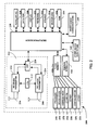
- Fig. 3 depicts the preferred structure for the multi-band slot-strip antenna 300.
- the secondary antenna 300 comprises a planar conductive layer 302.
- the planar conductive layer 302 is disposed on a substrate layer (not shown).
- the conductive layer 302 has a substantially rectangular shape having two opposing pairs of substantially parallel edges.
- the multi-band slot-strip antenna 300 is implemented as a printed circuit board, with the planar conductive layer 302 comprising copper or other suitable conductive metal.
- the conductive layer 302 comprises a conductive region 308 and three non-conductive regions (discussed below).
- the non-conductive region is devoid of conductive metal.
- the non-conductive region is implemented via suitable printed circuit board etching techniques.
- the non-conductive regions, together with the surrounding conductive region 308, define a first slot-strip structure 312, a second slot-strip structure 314 that is electrically coupled to the first slot-strip structure 312, and a third slot-strip structure 316 that is electrically coupled to the second slot-strip structure 314.
- the conductive-region 308 comprises a first L-shaped arm 318 (comprising a first linear (straight) minor arm portion 318a and a first linear (straight) major arm portion 318b); a second L-shaped arm 320 (comprising a second linear (straight) minor arm portion 320a and a second linear (straight) major arm portion 320b); a first linear (straight) arm 322 and a second linear (straight) arm 324.
- the conductive-region 308 also comprises a first rectangular base portion 326 that extends substantially perpendicularly between the first major arm portion 318 and the second major arm portion 320b of the L-shaped arms 318, 320; a second rectangular base portion 328 that extends substantially perpendicularly between the second major arm portion 320b and the first linear arm 322; and a third rectangular base portion 330 that extends substantially perpendicularly between the first and second linear arms 322, 324.
- the non-conductive region comprises a first non-conductive slot 332 (comprising first minor slot portion 332a and first major slot portion 332b), a second non-conductive slot 334 (comprising second minor slot portion 334a and second major slot portion 334b), and a third non-conductive slot 336.
- the first non-conductive slot 332 has a substantially L-shape, and extends between the first and second L-shaped arms 318, 320, terminating at the first base portion 326.
- the second non-conductive slot 334 also has a substantially L-shape, and extends between the second L-shaped arm 320, the third base portion 330 and the first linear arm 322, terminating at the second base portion 332.
- the third non-conductive slot 336 has a substantially linear (straight) shape, and extends between the first and second linear arms 322, 324, terminating at the third base portion 330.
- the first slot-strip structure 312 comprises the first L-shaped arm 318, the first base portion 326, the second base portion 328 and the first non-conductive slot 332.
- the second slot-strip structure 314 comprises the second L-shaped arm 320, the second base portion 328, the first linear arm 322, and the second non-conductive slot 334.
- the third slot-strip structure 316 comprises the first linear arm 322, the third base portion 330, the second linear arm 324, and the third non-conductive slot 336.
- first and second slot-strip structures 312, 314 are commonly coupled by the second L-shaped arm 320.
- the second and third slot-strip structures 314, 316 are commonly coupled by the first linear arm 322.
- the first, second and third slot-strip structures 312, 314, 316 are substantially U-shaped.
- the multi-band slot-strip antenna 300 also includes a signal feed pin 304, and first and second signal grounding pins 306a, 306b.
- the signal feed pin 304 is connected to the first minor arm portion 318a of the first slot-strip structure 312, 314, in close proximity to the open end of the first non-conductive slot 332.
- the first signal ground pin 306a is connected to the second minor arm portion 320a of the first and second slot-strip structures 312, 314, in close proximity to the signal feed pin 304 and the open end of the first non-conductive slot 332.
- the first signal ground pin 306a is also proximate the third base portion 330 of the third slot-strip structure 316.
- the second signal ground pin 306b is connected to the second linear arm 324 of the third slot-strip structure 316, in close proximity to the open end of the third non-conductive slot 336. As will become apparent, this second signal ground pin 306b extends the bandwidth of the lower frequency band of the multi-band slot-strip antenna 300 to cover most of the application bands at/near 2 GHz.
- the first minor arm portion 318a is substantially parallel to the second minor arm portion 320a; and the first major arm portion 318b is substantially parallel to the second major arm portion 320b.
- the first linear arm 322 is substantially parallel to the second major arm portion 320b, and the second linear arm 324 is substantially parallel to the first linear arm 322.
- first minor slot portion 332a is substantially parallel to the second minor slot portion 334a.
- first major slot portion 332b is substantially parallel to the second major slot portion 334b.
- second non-conductive slot 334 opens in substantially the same direction as the first non-conductive slot 332.
- the third non-conductive slot 336 is preferably substantially parallel to the second major slot portion 334b of the second non-conductive slot 334. However, the third non-conductive slot 336 opens in a direction that is substantially opposite to that of the second non-conductive slot 334.
- first and second minor arm portions 318a, 320a, the first and second minor slot portions 332a, 334a, and the rectangular base portions 326, 328, 330 are parallel to one pair of opposing edges of the conductive layer 302.
- first and second major arm portions 318b, 320b, the first and second linear arms 322, 324 and the rectangular base portions 326, 328, 330 are parallel to the other pair of opposing edges of the conductive layer 302.
- Fig. 4 to 8 are computer simulations of the return loss for the multi-band slot-strip antenna 300. In these simulations:
- Fig. 4 depicts the variation in return loss of the multi-band slot-strip antenna 300 with length L a .
- This simulation reveals that the length of the first major slot portion 332b has a preferential impact on the centre frequency and impedance of the lower frequency band, in comparison to the higher frequency band. This result is advantageous since it reveals that the frequency and impedance of the lower frequency band can be adjusted by varying the length of the first slot-strip structure 312, without significantly impacting the characteristics of the upper frequency band.
- Fig. 5 depicts the variation in return loss with length L b .
- L a 13.5mm
- L c 6.5mm
- h a 1mm
- h b 2mm
- h c 2mm
- This simulation reveals that the centre frequency, impedance and bandwidth of the upper and lower frequency bands are sensitive to variations in the length of the second major slot portion 334b.
- Fig. 6 depicts the variation in return loss with L c .
- This simulation reveals that the impedance of the upper and lower frequency bands is sensitive to variations in the length of the third non-conductive slot 336. This result is advantageous since it reveals that the impedance of both bands can be adjusted independently of the centre frequency and bandwidth of the upper and lower frequency bands.
- Fig. 7 is a computer simulation of the return loss for a preferred implementation of the multi-band slot-strip antenna 300, in comparison to a structure which has the same shape and dimensions but lacks the second signal grounding pin 306b.
- L a 13.5mm
- L b 28.5mm
- L c 6.5mm
- h a 1mm
- h b 2mm
- h c 2mm.
- This simulation reveals that the second signal grounding pin 306b adds two closely-spaced resonant frequencies to the simulated spectrum around 2GHz, which significantly increases the bandwidth of the low frequency range from about 250MHz to about 500MHz.
- This graph reveals that the multi-band slot-strip antenna 300 has an actual low frequency range that extends from 1.67 GHz to 2.34 GHz.
- the introduction of the second signal grounding pin 306b significantly enhances the multi-band performance of the multi-band slot-strip antenna 300.
- the graph also reveals that the multi-band slot-strip antenna 300 has a higher frequency (5GHz) range that is suitable for WLAN 802.11 a/j applications.
- the multi-band antenna 300 offers enhanced low frequency bandwidth around 2 GHz suitable for 3G communications. This result is obtained in a structure whose size is suitable for incorporation into small handheld communications devices.
Abstract
Description
- The invention described herein relates generally to a multi-band antenna for a handheld wireless communications device. In particular, the invention relates to a multi-band slot-strip antenna.
- Slot antennas typically comprise a slot cut into a metal sheet or printed circuit board. Since some modem communication devices are required to operate in multiple frequency bands, multi-band slot antennas have been developed for use in such devices.
- For instance, Chang (
US 7,006,048 ) describes a dual-band slot antenna for satellite and/or RFID communication systems. The slot antenna comprises two interconnected L-shaped slot antenna structures, and a printed circuit feed line that is coupled to both of the L-shaped slot antenna structures. Sun (US 6,677,909 ) describes dual-band slot antenna that comprises a pair of meandering slots, and a coaxial feed cable that is connected to the meandering slots. - Planar inverted-F antennas (PIFA) are becoming increasingly common in wireless handheld communication devices due to their reduced size in comparison to conventional microstrip antenna designs. Therefore, PIFA antennas have been developed which include multiple resonant sections, each having a respective resonant frequency. However, since conventional PIFA antennas have a very limited bandwidth, broadband technologies, such as parasitic elements and/or multi-layer structures, have been used to modify the conventional PIFA antenna for multi-band and broadband applications.
- These approaches increase the size of the antenna, making the resulting designs unattractive for modem handheld communication devices. Also, the additional resonant branches introduced by these approaches make the operational frequencies of the antennas difficult to tune. Further, the additional branches can introduce significant electromagnetic compatibility (EMC) and electromagnetic interference (EMI) problems.
- According to the invention described herein, a multi-band antenna may comprise at least three slot-strip structures configured with multiple ground pins.
- In accordance with a first aspect of the invention, there may be provided a multi-band slot-strip antenna that comprises a planar conductive layer comprising a conductive region and a non-conductive region. The conductive region and the non-conductive region together may define a first slot-strip structure, a second slot-strip structure coupled to the first slot-strip structure, and a third slot-strip structure coupled to the second slot-strip structure. The first slot-strip structure may comprise a signal feed portion. The second slot-strip structure may include a first signal grounding portion. The third slot-strip structure comprises a second signal grounding portion.
- In accordance with a second aspect of the invention, there may be provided a wireless communication device that comprises a radio transceiver section, and a multi-band slot-strip antenna coupled to the radio transceiver section. The multi-band slot-strip antenna may comprise a planar conductive layer comprising a conductive region and a non-conductive region. The conductive region and the non-conductive region together may define a first slot-strip structure, a second slot-strip structure coupled to the first slot-strip structure, and a third slot-strip structure coupled to the second slot-strip structure. The first slot-strip structure may comprise a signal feed portion. The second slot-strip structure may include a first signal grounding portion. The third slot-strip structure may comprise a second signal grounding portion. The signal feed portion may be coupled to the radio transceiver section.
- In accordance with a third aspect of the invention, there may be provided a multi-band slot-strip antenna that comprises a planar conductive layer comprising a conductive region and a non-conductive region. The conductive region and the non-conductive region together may define a plurality of mutually-coupled slot-strip structures. The slot-strip antenna also may comprise a feed signal pin connected to one of the slot-strip structures, and a ground pin connected to the other slot-strip structures.
- As will become apparent, in addition to a higher frequency band around 5 GHz for WLAN 802.11 j/a applications, the multi-band antenna offers enhanced low frequency bandwidth around 2 GHz for 3G communications, from a structure whose size is suitable for incorporation into small handheld communications devices.
- The invention will now be described, by way of example only, with reference to the accompanying drawings, in which:
-
Fig. 1 is a front plan view of a handheld communications device according to the invention; -
Fig. 2 is a schematic diagram depicting certain functional details of the handheld communications device; -
Fig. 3 is a top plan view of a multi-band slot-strip antenna of the handheld communications device, suitable for use with a wireless network; -
Fig. 4 to 6 are computer simulations of the return loss for the multi-band slot-strip antenna; -
Fig. 7 is a computer simulation of the return loss for a preferred implementation of the multi-band slot-strip antenna; and -
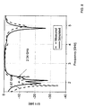
Fig. 8 depicts the computer simulated and actual return loss for the preferred implementation of the multi-band slot-strip antenna. - Turning to
Fig. 1 , there is shown a samplehandheld communications device 200 in accordance with the invention. Preferably, thehandheld communications device 200 is a two-way wireless communications device having at least voice and data communication capabilities, and is configured to operate within a wireless cellular network. Depending on the exact functionality provided, the wirelesshandheld communications device 200 may be referred to as a data messaging device, a two-way pager, a wireless e-mail device, a cellular telephone with data messaging capabilities, a wireless Internet appliance, or a data communication device, as examples. - As shown, the
handheld communications device 200 includes adisplay 222, afunction key 246, and data processing means (not shown) disposed within acommon housing 201. Thedisplay 222 comprises a backlit LCD display. The data processing means is in communication with thedisplay 222 and thefunction key 246. In one implementation, thebacklit display 222 comprises a transmissive LCD display, and thefunction key 246 operates as a power on/off switch. Alternately, in another implementation, thebacklit display 222 comprises a reflective or trans-reflective LCD display, and thefunction key 246 operates as a backlight switch. - In addition to the
display 222 and thefunction key 246, thehandheld communications device 200 includes user data input means for inputting data to the data processing means. As shown, preferably the user data input means includes akeyboard 232, athumbwheel 248 and anescape key 260. Thekeyboard 232 includes alphabetic and numerical keys, and preferably also includes a "Send" key and an "End" key to respectively initiate and terminate voice communication. However, the data input means is not limited to these forms of data input. For instance, the data input means may include a trackball or other pointing device instead of (or in addition to) thethumbwheel 248. -
Fig. 2 depicts functional details of thehandheld communications device 200. As shown, thehandheld communications device 200 incorporates a motherboard that includes acommunication subsystem 211, and amicroprocessor 238. Thecommunication subsystem 211 performs communication functions, such as data and voice communications, and includes a primary transmitter/receiver 212, a secondary transmitter/receiver 214, a primaryinternal antenna 216 for the primary transmitter/receiver 212, a secondaryinternal antenna 300 for the secondary transmitter/receiver 214, and local oscillators (LOs) 213 and one or more digital signal processors (DSP) 220 coupled to the transmitter/receivers - Typically, the
communication subsystem 211 sends and receives wireless communication signals over a wireless cellular network via the primary transmitter/receiver 212 and the primaryinternal antenna 216. Further, typically thecommunication subsystem 211 sends and receives wireless communication signals over a local area wireless network via the secondary transmitter/receiver 214 and the secondaryinternal antenna 300. - Preferably, the primary
internal antenna 216 is configured for use within a Global System for Mobile Communications (GSM) cellular network or a Code Division Multiple Access (CDMA) cellular network. Further, preferably the secondaryinternal antenna 300 is configured for use within a Universal Mobile Telecommunications Service (UMTS) or WLAN WiFi (IEEE 802.1 1x) network. More preferably, the secondaryinternal antenna 300 is a multi-band slot-strip antenna that is configured for use with networks whose operational frequencies are at/near 2GHz and 5 GHz, and whose low frequency bandwidth is suitable for 3G communications and high frequcny band for WLAN 802.11 j/a applications. Although thehandheld communications device 200 is depicted inFig. 2 with two antennas, it should be understood that thehandheld communications device 200 may instead comprise only a single antenna, with the multi-band slot-strip antenna 300 being connected to both the primary transmitter/receiver 212 and the secondary transmitter/receiver 214. Further, althoughFig. 2 depicts themulti-band antenna 300 incorporated into thehandheld communications device 200, themulti-band antenna 300 is not limited to mobile applications, but may instead by used with a stationary communications device. The preferred structure of themulti-band antenna 300 will be discussed in detail below, with reference toFigs. 3 to 8 . - Signals received by the primary
internal antenna 216 from the wireless cellular network are input to the receiver section of the primary transmitter/receiver 212, which performs common receiver functions such as frequency down conversion, and analog to digital (A/D) conversion, in preparation for more complex communication functions performed by theDSP 220. Signals to be transmitted over the wireless cellular network are processed by theDSP 220 and input to transmitter section of the primary transmitter/receiver 212 for digital to analog conversion, frequency up conversion, and transmission over the wireless cellular network via the primaryinternal antenna 216. - Similarly, signals received by the secondary
internal antenna 300 from the local area wireless network are input to the receiver section of the secondary transmitter/receiver 214, which performs common receiver functions such as frequency down conversion, and analog to digital (A/D) conversion, in preparation for more complex communication functions performed by theDSP 220. Signals to be transmitted over the local area wireless network are processed by theDSP 220 and input to transmitter section of the secondary transmitter/receiver 214 for digital to analog conversion, frequency up conversion, and transmission over the local area wireless network via the secondaryinternal antenna 300. If thecommunication subsystem 211 includes more than oneDSP 220, the signals transmitted and received by the secondary transmitter/receiver 214 would preferably be processed by a different DSP than the primary transmitter/receiver 212. - The
communications device 200 also includes aSIM interface 244 if thehandheld communications device 200 is configured for use within a GSM network, and/or aRUIM interface 244 if thehandheld communications device 200 is configured for use within a CDMA network. The SIM/RUIM interface 244 is similar to a card-slot into which a SIM/RUIM card can be inserted and ejected like a diskette or PCMCIA card. The SIM/RUIM card holds manykey configurations 251, andother information 253 including subscriber identification information, such as the International Mobile Subscriber Identity (IMSI) that is associated with thehandheld communications device 200, and subscriber-related information. - The
microprocessor 238, in conjunction with theflash memory 224 and theRAM 226, comprises the aforementioned data processing means and controls the overall operation of the device. The data processing means interacts with device subsystems such as thedisplay 222,flash memory 224,RAM 226, auxiliary input/output (I/O)subsystems 228,data port 230,keyboard 232,speaker 234,microphone 236, short-range communications subsystem 240, anddevice subsystems 242. Thedata port 230 may comprise a RS-232 port, a Universal Serial Bus (USB) port or other wired data communication port. - As shown, the
flash memory 224 includes bothcomputer program storage 258 andprogram data storage flash memory 224 or other similar non-volatile storage. Other computer processing instructions may also be loaded into a volatile memory such asRAM 226. The computer processing instructions, when accessed from thememory microprocessor 238 define an operating system, computer programs, operating system specific applications. The computer processing instructions may be installed onto thehandheld communications device 200 upon manufacture, or may be loaded through the cellular wireless network, the auxiliary I/O subsystem 228, thedata port 230, the short-range communications subsystem 240, or thedevice subsystem 242. - The operating system allows the
handheld communications device 200 to operate thedisplay 222, the auxiliary input/output (I/O)subsystems 228,data port 230,keyboard 232,speaker 234,microphone 236, short-range communications subsystem 240, anddevice subsystems 242. Typically, the computer programs include communication software that configures thehandheld communications device 200 to receive one or more communication services. For instance, preferably the communication software includes internet browser software, e-mail software and telephone software that respectively allow thehandheld communications device 200 to communicate with various computer servers over the internet, send and receive e-mail, and initiate and receive telephone calls. -
Fig. 3 depicts the preferred structure for the multi-band slot-strip antenna 300. Thesecondary antenna 300 comprises a planarconductive layer 302. Preferably, the planarconductive layer 302 is disposed on a substrate layer (not shown). As shown, theconductive layer 302 has a substantially rectangular shape having two opposing pairs of substantially parallel edges. Preferably, the multi-band slot-strip antenna 300 is implemented as a printed circuit board, with the planarconductive layer 302 comprising copper or other suitable conductive metal. - The
conductive layer 302 comprises aconductive region 308 and three non-conductive regions (discussed below). In contrast to theconductive region 308, the non-conductive region is devoid of conductive metal. Typically, the non-conductive region is implemented via suitable printed circuit board etching techniques. As shown, the non-conductive regions, together with the surroundingconductive region 308, define a first slot-strip structure 312, a second slot-strip structure 314 that is electrically coupled to the first slot-strip structure 312, and a third slot-strip structure 316 that is electrically coupled to the second slot-strip structure 314. - The conductive-
region 308 comprises a first L-shaped arm 318 (comprising a first linear (straight)minor arm portion 318a and a first linear (straight)major arm portion 318b); a second L-shaped arm 320 (comprising a second linear (straight)minor arm portion 320a and a second linear (straight)major arm portion 320b); a first linear (straight)arm 322 and a second linear (straight)arm 324. The conductive-region 308 also comprises a firstrectangular base portion 326 that extends substantially perpendicularly between the first major arm portion 318 and the secondmajor arm portion 320b of the L-shaped arms 318, 320; a secondrectangular base portion 328 that extends substantially perpendicularly between the secondmajor arm portion 320b and the firstlinear arm 322; and a thirdrectangular base portion 330 that extends substantially perpendicularly between the first and secondlinear arms - The non-conductive region comprises a first non-conductive slot 332 (comprising first
minor slot portion 332a and firstmajor slot portion 332b), a second non-conductive slot 334 (comprising secondminor slot portion 334a and secondmajor slot portion 334b), and a thirdnon-conductive slot 336. - The first non-conductive slot 332 has a substantially L-shape, and extends between the first and second L-shaped arms 318, 320, terminating at the
first base portion 326. The second non-conductive slot 334 also has a substantially L-shape, and extends between the second L-shaped arm 320, thethird base portion 330 and the firstlinear arm 322, terminating at the second base portion 332. The thirdnon-conductive slot 336 has a substantially linear (straight) shape, and extends between the first and secondlinear arms third base portion 330. - The first slot-
strip structure 312 comprises the first L-shaped arm 318, thefirst base portion 326, thesecond base portion 328 and the first non-conductive slot 332. The second slot-strip structure 314 comprises the second L-shaped arm 320, thesecond base portion 328, the firstlinear arm 322, and the second non-conductive slot 334. The third slot-strip structure 316 comprises the firstlinear arm 322, thethird base portion 330, the secondlinear arm 324, and the thirdnon-conductive slot 336. - With this configuration, the first and second slot-
strip structures strip structures linear arm 322. Further, the first, second and third slot-strip structures - As shown, the multi-band slot-
strip antenna 300 also includes asignal feed pin 304, and first and secondsignal grounding pins signal feed pin 304 is connected to the firstminor arm portion 318a of the first slot-strip structure signal ground pin 306a is connected to the secondminor arm portion 320a of the first and second slot-strip structures signal feed pin 304 and the open end of the first non-conductive slot 332. The firstsignal ground pin 306a is also proximate thethird base portion 330 of the third slot-strip structure 316. - The second
signal ground pin 306b is connected to the secondlinear arm 324 of the third slot-strip structure 316, in close proximity to the open end of the thirdnon-conductive slot 336. As will become apparent, this secondsignal ground pin 306b extends the bandwidth of the lower frequency band of the multi-band slot-strip antenna 300 to cover most of the application bands at/near 2 GHz. - Preferably, the first
minor arm portion 318a is substantially parallel to the secondminor arm portion 320a; and the firstmajor arm portion 318b is substantially parallel to the secondmajor arm portion 320b. Further, preferably the firstlinear arm 322 is substantially parallel to the secondmajor arm portion 320b, and the secondlinear arm 324 is substantially parallel to the firstlinear arm 322. - Similarly, the first
minor slot portion 332a is substantially parallel to the secondminor slot portion 334a. Similarly, preferably the firstmajor slot portion 332b is substantially parallel to the secondmajor slot portion 334b. Further, the second non-conductive slot 334 opens in substantially the same direction as the first non-conductive slot 332. - The third
non-conductive slot 336 is preferably substantially parallel to the secondmajor slot portion 334b of the second non-conductive slot 334. However, the thirdnon-conductive slot 336 opens in a direction that is substantially opposite to that of the second non-conductive slot 334. - Further, preferably the first and second
minor arm portions minor slot portions rectangular base portions conductive layer 302. In addition, preferably the first and secondmajor arm portions linear arms rectangular base portions conductive layer 302. -
Fig. 4 to 8 are computer simulations of the return loss for the multi-band slot-strip antenna 300. In these simulations: - La is the length of the first
major slot portion 332b - Lb is the length of the second
major slot portion 334b - Lc is the length of the third
non-conductive slot 336 - ha is the width of the first
major slot portion 332b - hb is the width of the second
major slot portion 334b - hc is the width of the third
non-conductive slot 336 -
Fig. 4 depicts the variation in return loss of the multi-band slot-strip antenna 300 with length La. In this simulation, Lb = 28.5mm; Lc = 6.5mm; ha = 1mm; hb = 2mm; hc = 2mm; and La3 > La2 > La1 . This simulation reveals that the length of the firstmajor slot portion 332b has a preferential impact on the centre frequency and impedance of the lower frequency band, in comparison to the higher frequency band. This result is advantageous since it reveals that the frequency and impedance of the lower frequency band can be adjusted by varying the length of the first slot-strip structure 312, without significantly impacting the characteristics of the upper frequency band. -
Fig. 5 depicts the variation in return loss with length Lb. In this simulation, La = 13.5mm; Lc = 6.5mm; ha = 1mm; hb = 2mm; hc = 2mm; and Lb4 > Lb3 > Lb2 > Lb1. This simulation reveals that the centre frequency, impedance and bandwidth of the upper and lower frequency bands are sensitive to variations in the length of the secondmajor slot portion 334b. -
Fig. 6 depicts the variation in return loss with Lc. In this simulation, La = 13.5mm; Lb = 28.5mm; ha = 1mm; hb = 2mm; hc = 2mm; and Lc1 > Lc2 > Lc3 > Lc4. This simulation reveals that the impedance of the upper and lower frequency bands is sensitive to variations in the length of the thirdnon-conductive slot 336. This result is advantageous since it reveals that the impedance of both bands can be adjusted independently of the centre frequency and bandwidth of the upper and lower frequency bands. -
Fig. 7 is a computer simulation of the return loss for a preferred implementation of the multi-band slot-strip antenna 300, in comparison to a structure which has the same shape and dimensions but lacks the secondsignal grounding pin 306b. In this simulation, La = 13.5mm; Lb = 28.5mm; Lc = 6.5mm; ha = 1mm; hb = 2mm; hc = 2mm. This simulation reveals that the secondsignal grounding pin 306b adds two closely-spaced resonant frequencies to the simulated spectrum around 2GHz, which significantly increases the bandwidth of the low frequency range from about 250MHz to about 500MHz. -
Fig. 8 depicts the computer simulated and actual performance of a secondary multi-band slot-strip antenna 300 having the following dimensions: La = 13.5mm; Lb = 28.5mm; Lc = 6.5mm; ha = 1mm; hb = 2mm; hc = 2mm. This graph reveals that the multi-band slot-strip antenna 300 has an actual low frequency range that extends from 1.67 GHz to 2.34 GHz. Since the GSM1800 band (1710-1880MHz), the GSM1900 band (1850-1990MHz), the DCS band (1710-1880MHz), the PCS band (1880-1990MHz), and the UMTS band (1900-2200MHz) all fall within this enhanced low frequency range of the multi-band slot-strip antenna 300, the introduction of the secondsignal grounding pin 306b significantly enhances the multi-band performance of the multi-band slot-strip antenna 300. The graph also reveals that the multi-band slot-strip antenna 300 has a higher frequency (5GHz) range that is suitable for WLAN 802.11 a/j applications. - As will be appreciated from the foregoing discussion, the
multi-band antenna 300 offers enhanced low frequency bandwidth around 2 GHz suitable for 3G communications. This result is obtained in a structure whose size is suitable for incorporation into small handheld communications devices. - The scope of the monopoly desired for the invention is defined by the claims appended hereto, with the foregoing description being merely illustrative of the preferred embodiment of the invention. Persons of ordinary skill may envisage modifications to the described embodiment which, although not explicitly suggested herein, do not depart from the scope of the invention, as defined by the appended claims.
Claims (12)
- A multi-band slot-strip antenna comprising:a planar conductive layer comprising a conductive region and a non-conductive region, the conductive region and the non-conductive region together defining a first slot-strip structure comprising a signal feed portion; a second slot-strip structure coupled to the first slot-strip structure, the second slot-strip structure comprising a first signal grounding portion; and a third slot-strip structure coupled to the second slot-strip structure, the third slot-strip structure comprising a second signal grounding portion.
- The multi-band antenna according to Claim 1, wherein the slot-strip structures each have a substantially U-shape, each said U-shaped slot-strip structure comprising a pair of substantially parallel arms, a base portion joining together the arms, and a slot extending between the arms, the slot of the third slot-strip structure opening in a direction opposite to that of the second slot-strip structure.
- The multi-band antenna according to Claim 2, wherein the slot of the second slot-strip structure opens in a direction substantially the same as that of the first slot-strip structure.
- The multi-band antenna according to Claim 2 or Claim 3, wherein the signal feed portion and the grounding portions are disposed proximate an end of one arm of the respective slot-strip structures, and the first grounding portion is disposed proximate the signal feed portion.
- The multi-band antenna according to any one of Claims 2 to 4, wherein the first grounding portion is disposed proximate the base portion of the third slot-strip structure.
- The multi-band antenna according to Claim 2, wherein the signal feed portion and the grounding portions are disposed proximate an end of one arm of the respective slot-strip structures, and the first grounding portion is disposed proximate the signal feed portion.
- The multi-band antenna according to Claim 6, wherein the first grounding portion is disposed proximate the base portion of the third slot-strip structure.
- The multi-band antenna according to any one of Claims 2 to 7, wherein the slot-strip structures are coupled together at their respective arms.
- The multi-band antenna according to Claim 8, wherein the arms of the first slot-strip structure have a substantially L-shape.
- The multi-band antenna according to Claim 9, wherein one arm of the second slot-strip structure has a substantially L-shape, and the other arm of the second slot-strip structure has a substantially linear shape.
- A wireless communications device comprising:a radio transceiver section; anda multi-band slot-strip antenna according to any one of Claims 1 to 10, the multi-band slot-strip antenna being coupled to the radio transceiver section.
- A multi-band slot-strip antenna comprising:a planar conductive layer comprising a conductive region and a central non-conductive region, the conductive region and the non-conductive region together defining at least three mutually-coupled slot-strip structures;a feed signal pin connected to one of the slot-strip structures; anda ground pin connected to the other slot-strip structures.
Priority Applications (5)
| Application Number | Priority Date | Filing Date | Title |
|---|---|---|---|
| DE602007007184T DE602007007184D1 (en) | 2007-03-19 | 2007-03-19 | Multi-band antenna with slot strips |
| EP07104442A EP1973197B1 (en) | 2007-03-19 | 2007-03-19 | Multi-band slot-strip antenna |
| AT07104442T ATE471581T1 (en) | 2007-03-19 | 2007-03-19 | MULTI-BAND ANTENNA WITH SLOTTED STRIPS |
| CA2684588A CA2684588C (en) | 2007-03-19 | 2008-03-19 | Multi-band slot-strip antenna |
| PCT/CA2008/000520 WO2008113171A1 (en) | 2007-03-19 | 2008-03-19 | Multi-band slot-strip antenna |
Applications Claiming Priority (1)
| Application Number | Priority Date | Filing Date | Title |
|---|---|---|---|
| EP07104442A EP1973197B1 (en) | 2007-03-19 | 2007-03-19 | Multi-band slot-strip antenna |
Publications (2)
| Publication Number | Publication Date |
|---|---|
| EP1973197A1 true EP1973197A1 (en) | 2008-09-24 |
| EP1973197B1 EP1973197B1 (en) | 2010-06-16 |
Family
ID=38236419
Family Applications (1)
| Application Number | Title | Priority Date | Filing Date |
|---|---|---|---|
| EP07104442A Active EP1973197B1 (en) | 2007-03-19 | 2007-03-19 | Multi-band slot-strip antenna |
Country Status (5)
| Country | Link |
|---|---|
| EP (1) | EP1973197B1 (en) |
| AT (1) | ATE471581T1 (en) |
| CA (1) | CA2684588C (en) |
| DE (1) | DE602007007184D1 (en) |
| WO (1) | WO2008113171A1 (en) |
Cited By (1)
| Publication number | Priority date | Publication date | Assignee | Title |
|---|---|---|---|---|
| WO2013155015A1 (en) * | 2012-04-09 | 2013-10-17 | Maxtena, Inc. | Antenna surrounded by metal housing |
Families Citing this family (1)
| Publication number | Priority date | Publication date | Assignee | Title |
|---|---|---|---|---|
| CN107221739B (en) * | 2017-06-12 | 2023-02-14 | 华南理工大学 | RFID reader antenna based on orthogonal slot technology |
Citations (6)
| Publication number | Priority date | Publication date | Assignee | Title |
|---|---|---|---|---|
| EP0923156A1 (en) | 1997-12-11 | 1999-06-16 | Alcatel | Shorted microstrip antenna and apparatus using the same |
| EP1304765A2 (en) * | 2001-10-22 | 2003-04-23 | Filtronic LK Oy | Internal multiband antenna |
| US6677909B2 (en) | 2001-11-09 | 2004-01-13 | Hon Hai Precision Ind. Co., Ltd. | Dual band slot antenna with single feed line |
| US20040085244A1 (en) | 2002-11-06 | 2004-05-06 | Kadambi Govind Rangaswamy | Planar inverted-f-antenna (pifa) having a slotted radiating element providing global cellular and gps-bluetooth frequency response |
| WO2004049501A1 (en) * | 2002-11-28 | 2004-06-10 | Research In Motion Limited | Multiple-band antenna with patch and slot structures |
| US7006048B2 (en) | 2003-09-15 | 2006-02-28 | Tatung Co., Ltd. | Dual operational frequency slot antenna |
Family Cites Families (2)
| Publication number | Priority date | Publication date | Assignee | Title |
|---|---|---|---|---|
| US7202831B2 (en) * | 2005-08-09 | 2007-04-10 | Darts Technologies Corp. | Multi-band frequency loop-slot antenna |
| US7176838B1 (en) * | 2005-08-22 | 2007-02-13 | Motorola, Inc. | Multi-band antenna |
-
2007
- 2007-03-19 DE DE602007007184T patent/DE602007007184D1/en active Active
- 2007-03-19 EP EP07104442A patent/EP1973197B1/en active Active
- 2007-03-19 AT AT07104442T patent/ATE471581T1/en not_active IP Right Cessation
-
2008
- 2008-03-19 CA CA2684588A patent/CA2684588C/en active Active
- 2008-03-19 WO PCT/CA2008/000520 patent/WO2008113171A1/en active Application Filing
Patent Citations (6)
| Publication number | Priority date | Publication date | Assignee | Title |
|---|---|---|---|---|
| EP0923156A1 (en) | 1997-12-11 | 1999-06-16 | Alcatel | Shorted microstrip antenna and apparatus using the same |
| EP1304765A2 (en) * | 2001-10-22 | 2003-04-23 | Filtronic LK Oy | Internal multiband antenna |
| US6677909B2 (en) | 2001-11-09 | 2004-01-13 | Hon Hai Precision Ind. Co., Ltd. | Dual band slot antenna with single feed line |
| US20040085244A1 (en) | 2002-11-06 | 2004-05-06 | Kadambi Govind Rangaswamy | Planar inverted-f-antenna (pifa) having a slotted radiating element providing global cellular and gps-bluetooth frequency response |
| WO2004049501A1 (en) * | 2002-11-28 | 2004-06-10 | Research In Motion Limited | Multiple-band antenna with patch and slot structures |
| US7006048B2 (en) | 2003-09-15 | 2006-02-28 | Tatung Co., Ltd. | Dual operational frequency slot antenna |
Non-Patent Citations (1)
| Title |
|---|
| KADAMBI G R ET AL: "Applications of annular and L-shaped slot in PIFA design", IEEE ANTENNAS AND PROPAGATION SOCIETY INTERNATIONAL SYMPOSIUM. 2003 DIGEST. APS. COLUMBUS, OH, JUNE 22 - 27, 2003, NEW YORK, NY : IEEE, US, vol. VOL. 4 OF 4, 22 June 2003 (2003-06-22), pages 86, XP010747200, ISBN: 0-7803-7846-6 * |
Cited By (2)
| Publication number | Priority date | Publication date | Assignee | Title |
|---|---|---|---|---|
| WO2013155015A1 (en) * | 2012-04-09 | 2013-10-17 | Maxtena, Inc. | Antenna surrounded by metal housing |
| US9502776B2 (en) | 2012-04-09 | 2016-11-22 | Maxtena | Antenna surrounded by metal housing |
Also Published As
| Publication number | Publication date |
|---|---|
| CA2684588A1 (en) | 2008-09-25 |
| CA2684588C (en) | 2012-08-07 |
| DE602007007184D1 (en) | 2010-07-29 |
| WO2008113171A1 (en) | 2008-09-25 |
| ATE471581T1 (en) | 2010-07-15 |
| EP1973197B1 (en) | 2010-06-16 |
Similar Documents
| Publication | Publication Date | Title |
|---|---|---|
| US7777684B2 (en) | Multi-band slot-strip antenna | |
| US7773040B2 (en) | Dual-band F-slot patch antenna | |
| US7319432B2 (en) | Multiband planar built-in radio antenna with inverted-L main and parasitic radiators | |
| US7415248B2 (en) | Multiband radio antenna with a flat parasitic element | |
| US6614400B2 (en) | Antenna | |
| US7161541B2 (en) | Mobile telecommunication device and planar antenna thereof | |
| Ren | Ceramic based small LTE MIMO handset antenna | |
| CN102099962B (en) | Antenna arrangement | |
| US20100328164A1 (en) | Switched antenna with an ultra wideband feed element | |
| US20070273606A1 (en) | Multi mode antenna system | |
| US20020180648A1 (en) | Wireless terminal | |
| CN211404721U (en) | Communication device with antenna window | |
| EP1641077B1 (en) | Mobile telecommunication device and planar antenna therefor | |
| KR20090031969A (en) | Antenna element and wideband antenna device | |
| WO2008122317A1 (en) | A radio antenna for a communication terminal | |
| EP2385578B1 (en) | Dual-band F-slot patch antenna | |
| EP1345282B1 (en) | Multiband planar built-in radio antenna with inverted-l main and parasitic radiators | |
| EP1414106B1 (en) | Multiband radio antenna | |
| EP1973197B1 (en) | Multi-band slot-strip antenna | |
| CN1871742B (en) | Multi-band antennas and radio apparatus incorporating the same | |
| Sanad | Novel wideband MIMO antennas that can cover the whole LTE spectrum in handsets and portable computers | |
| Nepa et al. | A dual-band antenna for wireless communication terminals | |
| EP1443595A1 (en) | Antenna | |
| CN112397888B (en) | Mobile device | |
| Nepa et al. | A compact multi band PIFA for wireless LAN mobile terminals |
Legal Events
| Date | Code | Title | Description |
|---|---|---|---|
| PUAI | Public reference made under article 153(3) epc to a published international application that has entered the european phase |
Free format text: ORIGINAL CODE: 0009012 |
|
| 17P | Request for examination filed |
Effective date: 20070319 |
|
| AK | Designated contracting states |
Kind code of ref document: A1 Designated state(s): AT BE BG CH CY CZ DE DK EE ES FI FR GB GR HU IE IS IT LI LT LU LV MC MT NL PL PT RO SE SI SK TR |
|
| AX | Request for extension of the european patent |
Extension state: AL BA HR MK RS |
|
| 17Q | First examination report despatched |
Effective date: 20090416 |
|
| AKX | Designation fees paid |
Designated state(s): AT BE BG CH CY CZ DE DK EE ES FI FR GB GR HU IE IS IT LI LT LU LV MC MT NL PL PT RO SE SI SK TR |
|
| AXX | Extension fees paid |
Extension state: HR Payment date: 20070319 Extension state: BA Payment date: 20070319 Extension state: AL Payment date: 20070319 Extension state: MK Payment date: 20070319 Extension state: RS Payment date: 20070319 |
|
| GRAP | Despatch of communication of intention to grant a patent |
Free format text: ORIGINAL CODE: EPIDOSNIGR1 |
|
| GRAS | Grant fee paid |
Free format text: ORIGINAL CODE: EPIDOSNIGR3 |
|
| GRAA | (expected) grant |
Free format text: ORIGINAL CODE: 0009210 |
|
| AK | Designated contracting states |
Kind code of ref document: B1 Designated state(s): AT BE BG CH CY CZ DE DK EE ES FI FR GB GR HU IE IS IT LI LT LU LV MC MT NL PL PT RO SE SI SK TR |
|
| AX | Request for extension of the european patent |
Extension state: AL BA HR MK RS |
|
| REG | Reference to a national code |
Ref country code: CH Ref legal event code: EP |
|
| REG | Reference to a national code |
Ref country code: IE Ref legal event code: FG4D |
|
| REF | Corresponds to: |
Ref document number: 602007007184 Country of ref document: DE Date of ref document: 20100729 Kind code of ref document: P |
|
| REG | Reference to a national code |
Ref country code: NL Ref legal event code: VDEP Effective date: 20100616 |
|
| PG25 | Lapsed in a contracting state [announced via postgrant information from national office to epo] |
Ref country code: LT Free format text: LAPSE BECAUSE OF FAILURE TO SUBMIT A TRANSLATION OF THE DESCRIPTION OR TO PAY THE FEE WITHIN THE PRESCRIBED TIME-LIMIT Effective date: 20100616 Ref country code: SE Free format text: LAPSE BECAUSE OF FAILURE TO SUBMIT A TRANSLATION OF THE DESCRIPTION OR TO PAY THE FEE WITHIN THE PRESCRIBED TIME-LIMIT Effective date: 20100616 |
|
| LTIE | Lt: invalidation of european patent or patent extension |
Effective date: 20100616 |
|
| PG25 | Lapsed in a contracting state [announced via postgrant information from national office to epo] |
Ref country code: AT Free format text: LAPSE BECAUSE OF FAILURE TO SUBMIT A TRANSLATION OF THE DESCRIPTION OR TO PAY THE FEE WITHIN THE PRESCRIBED TIME-LIMIT Effective date: 20100616 Ref country code: SI Free format text: LAPSE BECAUSE OF FAILURE TO SUBMIT A TRANSLATION OF THE DESCRIPTION OR TO PAY THE FEE WITHIN THE PRESCRIBED TIME-LIMIT Effective date: 20100616 Ref country code: FI Free format text: LAPSE BECAUSE OF FAILURE TO SUBMIT A TRANSLATION OF THE DESCRIPTION OR TO PAY THE FEE WITHIN THE PRESCRIBED TIME-LIMIT Effective date: 20100616 Ref country code: LV Free format text: LAPSE BECAUSE OF FAILURE TO SUBMIT A TRANSLATION OF THE DESCRIPTION OR TO PAY THE FEE WITHIN THE PRESCRIBED TIME-LIMIT Effective date: 20100616 |
|
| PG25 | Lapsed in a contracting state [announced via postgrant information from national office to epo] |
Ref country code: CY Free format text: LAPSE BECAUSE OF FAILURE TO SUBMIT A TRANSLATION OF THE DESCRIPTION OR TO PAY THE FEE WITHIN THE PRESCRIBED TIME-LIMIT Effective date: 20100616 Ref country code: PL Free format text: LAPSE BECAUSE OF FAILURE TO SUBMIT A TRANSLATION OF THE DESCRIPTION OR TO PAY THE FEE WITHIN THE PRESCRIBED TIME-LIMIT Effective date: 20100616 |
|
| PG25 | Lapsed in a contracting state [announced via postgrant information from national office to epo] |
Ref country code: NL Free format text: LAPSE BECAUSE OF FAILURE TO SUBMIT A TRANSLATION OF THE DESCRIPTION OR TO PAY THE FEE WITHIN THE PRESCRIBED TIME-LIMIT Effective date: 20100616 Ref country code: GR Free format text: LAPSE BECAUSE OF FAILURE TO SUBMIT A TRANSLATION OF THE DESCRIPTION OR TO PAY THE FEE WITHIN THE PRESCRIBED TIME-LIMIT Effective date: 20100917 Ref country code: EE Free format text: LAPSE BECAUSE OF FAILURE TO SUBMIT A TRANSLATION OF THE DESCRIPTION OR TO PAY THE FEE WITHIN THE PRESCRIBED TIME-LIMIT Effective date: 20100616 |
|
| PG25 | Lapsed in a contracting state [announced via postgrant information from national office to epo] |
Ref country code: RO Free format text: LAPSE BECAUSE OF FAILURE TO SUBMIT A TRANSLATION OF THE DESCRIPTION OR TO PAY THE FEE WITHIN THE PRESCRIBED TIME-LIMIT Effective date: 20100616 Ref country code: BE Free format text: LAPSE BECAUSE OF FAILURE TO SUBMIT A TRANSLATION OF THE DESCRIPTION OR TO PAY THE FEE WITHIN THE PRESCRIBED TIME-LIMIT Effective date: 20100616 Ref country code: CZ Free format text: LAPSE BECAUSE OF FAILURE TO SUBMIT A TRANSLATION OF THE DESCRIPTION OR TO PAY THE FEE WITHIN THE PRESCRIBED TIME-LIMIT Effective date: 20100616 Ref country code: IS Free format text: LAPSE BECAUSE OF FAILURE TO SUBMIT A TRANSLATION OF THE DESCRIPTION OR TO PAY THE FEE WITHIN THE PRESCRIBED TIME-LIMIT Effective date: 20101016 Ref country code: PT Free format text: LAPSE BECAUSE OF FAILURE TO SUBMIT A TRANSLATION OF THE DESCRIPTION OR TO PAY THE FEE WITHIN THE PRESCRIBED TIME-LIMIT Effective date: 20101018 Ref country code: SK Free format text: LAPSE BECAUSE OF FAILURE TO SUBMIT A TRANSLATION OF THE DESCRIPTION OR TO PAY THE FEE WITHIN THE PRESCRIBED TIME-LIMIT Effective date: 20100616 |
|
| PG25 | Lapsed in a contracting state [announced via postgrant information from national office to epo] |
Ref country code: IT Free format text: LAPSE BECAUSE OF FAILURE TO SUBMIT A TRANSLATION OF THE DESCRIPTION OR TO PAY THE FEE WITHIN THE PRESCRIBED TIME-LIMIT Effective date: 20100616 |
|
| PLBE | No opposition filed within time limit |
Free format text: ORIGINAL CODE: 0009261 |
|
| STAA | Information on the status of an ep patent application or granted ep patent |
Free format text: STATUS: NO OPPOSITION FILED WITHIN TIME LIMIT |
|
| PG25 | Lapsed in a contracting state [announced via postgrant information from national office to epo] |
Ref country code: DK Free format text: LAPSE BECAUSE OF FAILURE TO SUBMIT A TRANSLATION OF THE DESCRIPTION OR TO PAY THE FEE WITHIN THE PRESCRIBED TIME-LIMIT Effective date: 20100616 |
|
| 26N | No opposition filed |
Effective date: 20110317 |
|
| REG | Reference to a national code |
Ref country code: DE Ref legal event code: R097 Ref document number: 602007007184 Country of ref document: DE Effective date: 20110316 |
|
| PG25 | Lapsed in a contracting state [announced via postgrant information from national office to epo] |
Ref country code: MC Free format text: LAPSE BECAUSE OF NON-PAYMENT OF DUE FEES Effective date: 20110331 |
|
| REG | Reference to a national code |
Ref country code: CH Ref legal event code: PL |
|
| PG25 | Lapsed in a contracting state [announced via postgrant information from national office to epo] |
Ref country code: MT Free format text: LAPSE BECAUSE OF FAILURE TO SUBMIT A TRANSLATION OF THE DESCRIPTION OR TO PAY THE FEE WITHIN THE PRESCRIBED TIME-LIMIT Effective date: 20100616 |
|
| REG | Reference to a national code |
Ref country code: IE Ref legal event code: MM4A |
|
| PG25 | Lapsed in a contracting state [announced via postgrant information from national office to epo] |
Ref country code: IE Free format text: LAPSE BECAUSE OF NON-PAYMENT OF DUE FEES Effective date: 20110319 Ref country code: LI Free format text: LAPSE BECAUSE OF NON-PAYMENT OF DUE FEES Effective date: 20110331 Ref country code: CH Free format text: LAPSE BECAUSE OF NON-PAYMENT OF DUE FEES Effective date: 20110331 |
|
| PG25 | Lapsed in a contracting state [announced via postgrant information from national office to epo] |
Ref country code: LU Free format text: LAPSE BECAUSE OF NON-PAYMENT OF DUE FEES Effective date: 20110319 |
|
| PG25 | Lapsed in a contracting state [announced via postgrant information from national office to epo] |
Ref country code: BG Free format text: LAPSE BECAUSE OF FAILURE TO SUBMIT A TRANSLATION OF THE DESCRIPTION OR TO PAY THE FEE WITHIN THE PRESCRIBED TIME-LIMIT Effective date: 20100916 Ref country code: TR Free format text: LAPSE BECAUSE OF FAILURE TO SUBMIT A TRANSLATION OF THE DESCRIPTION OR TO PAY THE FEE WITHIN THE PRESCRIBED TIME-LIMIT Effective date: 20100616 |
|
| PG25 | Lapsed in a contracting state [announced via postgrant information from national office to epo] |
Ref country code: ES Free format text: LAPSE BECAUSE OF FAILURE TO SUBMIT A TRANSLATION OF THE DESCRIPTION OR TO PAY THE FEE WITHIN THE PRESCRIBED TIME-LIMIT Effective date: 20100927 Ref country code: HU Free format text: LAPSE BECAUSE OF FAILURE TO SUBMIT A TRANSLATION OF THE DESCRIPTION OR TO PAY THE FEE WITHIN THE PRESCRIBED TIME-LIMIT Effective date: 20100616 |
|
| REG | Reference to a national code |
Ref country code: DE Ref legal event code: R082 Ref document number: 602007007184 Country of ref document: DE Representative=s name: MERH-IP MATIAS ERNY REICHL HOFFMANN, DE |
|
| REG | Reference to a national code |
Ref country code: DE Ref legal event code: R082 Ref document number: 602007007184 Country of ref document: DE Representative=s name: MERH-IP MATIAS ERNY REICHL HOFFMANN, DE Effective date: 20140925 Ref country code: DE Ref legal event code: R081 Ref document number: 602007007184 Country of ref document: DE Owner name: BLACKBERRY LIMITED, WATERLOO, CA Free format text: FORMER OWNER: RESEARCH IN MOTION LTD., WATERLOO, ONTARIO, CA Effective date: 20140925 Ref country code: DE Ref legal event code: R082 Ref document number: 602007007184 Country of ref document: DE Representative=s name: MERH-IP MATIAS ERNY REICHL HOFFMANN PATENTANWA, DE Effective date: 20140925 |
|
| REG | Reference to a national code |
Ref country code: FR Ref legal event code: PLFP Year of fee payment: 10 |
|
| REG | Reference to a national code |
Ref country code: FR Ref legal event code: PLFP Year of fee payment: 11 |
|
| REG | Reference to a national code |
Ref country code: FR Ref legal event code: PLFP Year of fee payment: 12 |
|
| PGFP | Annual fee paid to national office [announced via postgrant information from national office to epo] |
Ref country code: FR Payment date: 20230327 Year of fee payment: 17 |
|
| PGFP | Annual fee paid to national office [announced via postgrant information from national office to epo] |
Ref country code: GB Payment date: 20230327 Year of fee payment: 17 Ref country code: DE Payment date: 20230329 Year of fee payment: 17 |