EP1978796B1 - Multilayer printed wiring board and method for producing the same - Google Patents
Multilayer printed wiring board and method for producing the same Download PDFInfo
- Publication number
- EP1978796B1 EP1978796B1 EP08160500A EP08160500A EP1978796B1 EP 1978796 B1 EP1978796 B1 EP 1978796B1 EP 08160500 A EP08160500 A EP 08160500A EP 08160500 A EP08160500 A EP 08160500A EP 1978796 B1 EP1978796 B1 EP 1978796B1
- Authority
- EP
- European Patent Office
- Prior art keywords
- layer
- resin
- conductor circuit
- conductor
- multilayer printed
- Prior art date
- Legal status (The legal status is an assumption and is not a legal conclusion. Google has not performed a legal analysis and makes no representation as to the accuracy of the status listed.)
- Expired - Lifetime
Links
Images


Classifications
-
- H—ELECTRICITY
- H05—ELECTRIC TECHNIQUES NOT OTHERWISE PROVIDED FOR
- H05K—PRINTED CIRCUITS; CASINGS OR CONSTRUCTIONAL DETAILS OF ELECTRIC APPARATUS; MANUFACTURE OF ASSEMBLAGES OF ELECTRICAL COMPONENTS
- H05K3/00—Apparatus or processes for manufacturing printed circuits
- H05K3/46—Manufacturing multilayer circuits
-
- C—CHEMISTRY; METALLURGY
- C23—COATING METALLIC MATERIAL; COATING MATERIAL WITH METALLIC MATERIAL; CHEMICAL SURFACE TREATMENT; DIFFUSION TREATMENT OF METALLIC MATERIAL; COATING BY VACUUM EVAPORATION, BY SPUTTERING, BY ION IMPLANTATION OR BY CHEMICAL VAPOUR DEPOSITION, IN GENERAL; INHIBITING CORROSION OF METALLIC MATERIAL OR INCRUSTATION IN GENERAL
- C23G—CLEANING OR DE-GREASING OF METALLIC MATERIAL BY CHEMICAL METHODS OTHER THAN ELECTROLYSIS
- C23G1/00—Cleaning or pickling metallic material with solutions or molten salts
- C23G1/02—Cleaning or pickling metallic material with solutions or molten salts with acid solutions
- C23G1/10—Other heavy metals
-
- H—ELECTRICITY
- H05—ELECTRIC TECHNIQUES NOT OTHERWISE PROVIDED FOR
- H05K—PRINTED CIRCUITS; CASINGS OR CONSTRUCTIONAL DETAILS OF ELECTRIC APPARATUS; MANUFACTURE OF ASSEMBLAGES OF ELECTRICAL COMPONENTS
- H05K3/00—Apparatus or processes for manufacturing printed circuits
- H05K3/02—Apparatus or processes for manufacturing printed circuits in which the conductive material is applied to the surface of the insulating support and is thereafter removed from such areas of the surface which are not intended for current conducting or shielding
- H05K3/06—Apparatus or processes for manufacturing printed circuits in which the conductive material is applied to the surface of the insulating support and is thereafter removed from such areas of the surface which are not intended for current conducting or shielding the conductive material being removed chemically or electrolytically, e.g. by photo-etch process
- H05K3/067—Etchants
-
- H—ELECTRICITY
- H05—ELECTRIC TECHNIQUES NOT OTHERWISE PROVIDED FOR
- H05K—PRINTED CIRCUITS; CASINGS OR CONSTRUCTIONAL DETAILS OF ELECTRIC APPARATUS; MANUFACTURE OF ASSEMBLAGES OF ELECTRICAL COMPONENTS
- H05K3/00—Apparatus or processes for manufacturing printed circuits
- H05K3/10—Apparatus or processes for manufacturing printed circuits in which conductive material is applied to the insulating support in such a manner as to form the desired conductive pattern
- H05K3/108—Apparatus or processes for manufacturing printed circuits in which conductive material is applied to the insulating support in such a manner as to form the desired conductive pattern by semi-additive methods; masks therefor
-
- H—ELECTRICITY
- H05—ELECTRIC TECHNIQUES NOT OTHERWISE PROVIDED FOR
- H05K—PRINTED CIRCUITS; CASINGS OR CONSTRUCTIONAL DETAILS OF ELECTRIC APPARATUS; MANUFACTURE OF ASSEMBLAGES OF ELECTRICAL COMPONENTS
- H05K3/00—Apparatus or processes for manufacturing printed circuits
- H05K3/38—Improvement of the adhesion between the insulating substrate and the metal
- H05K3/382—Improvement of the adhesion between the insulating substrate and the metal by special treatment of the metal
- H05K3/384—Improvement of the adhesion between the insulating substrate and the metal by special treatment of the metal by plating
-
- H—ELECTRICITY
- H05—ELECTRIC TECHNIQUES NOT OTHERWISE PROVIDED FOR
- H05K—PRINTED CIRCUITS; CASINGS OR CONSTRUCTIONAL DETAILS OF ELECTRIC APPARATUS; MANUFACTURE OF ASSEMBLAGES OF ELECTRICAL COMPONENTS
- H05K3/00—Apparatus or processes for manufacturing printed circuits
- H05K3/38—Improvement of the adhesion between the insulating substrate and the metal
- H05K3/382—Improvement of the adhesion between the insulating substrate and the metal by special treatment of the metal
- H05K3/385—Improvement of the adhesion between the insulating substrate and the metal by special treatment of the metal by conversion of the surface of the metal, e.g. by oxidation, whether or not followed by reaction or removal of the converted layer
-
- H—ELECTRICITY
- H05—ELECTRIC TECHNIQUES NOT OTHERWISE PROVIDED FOR
- H05K—PRINTED CIRCUITS; CASINGS OR CONSTRUCTIONAL DETAILS OF ELECTRIC APPARATUS; MANUFACTURE OF ASSEMBLAGES OF ELECTRICAL COMPONENTS
- H05K3/00—Apparatus or processes for manufacturing printed circuits
- H05K3/38—Improvement of the adhesion between the insulating substrate and the metal
- H05K3/388—Improvement of the adhesion between the insulating substrate and the metal by the use of a metallic or inorganic thin film adhesion layer
-
- H—ELECTRICITY
- H05—ELECTRIC TECHNIQUES NOT OTHERWISE PROVIDED FOR
- H05K—PRINTED CIRCUITS; CASINGS OR CONSTRUCTIONAL DETAILS OF ELECTRIC APPARATUS; MANUFACTURE OF ASSEMBLAGES OF ELECTRICAL COMPONENTS
- H05K3/00—Apparatus or processes for manufacturing printed circuits
- H05K3/46—Manufacturing multilayer circuits
- H05K3/4644—Manufacturing multilayer circuits by building the multilayer layer by layer, i.e. build-up multilayer circuits
-
- H—ELECTRICITY
- H01—ELECTRIC ELEMENTS
- H01L—SEMICONDUCTOR DEVICES NOT COVERED BY CLASS H10
- H01L2924/00—Indexing scheme for arrangements or methods for connecting or disconnecting semiconductor or solid-state bodies as covered by H01L24/00
- H01L2924/0001—Technical content checked by a classifier
- H01L2924/0002—Not covered by any one of groups H01L24/00, H01L24/00 and H01L2224/00
-
- H—ELECTRICITY
- H05—ELECTRIC TECHNIQUES NOT OTHERWISE PROVIDED FOR
- H05K—PRINTED CIRCUITS; CASINGS OR CONSTRUCTIONAL DETAILS OF ELECTRIC APPARATUS; MANUFACTURE OF ASSEMBLAGES OF ELECTRICAL COMPONENTS
- H05K2201/00—Indexing scheme relating to printed circuits covered by H05K1/00
- H05K2201/01—Dielectrics
- H05K2201/0104—Properties and characteristics in general
- H05K2201/0129—Thermoplastic polymer, e.g. auto-adhesive layer; Shaping of thermoplastic polymer
-
- H—ELECTRICITY
- H05—ELECTRIC TECHNIQUES NOT OTHERWISE PROVIDED FOR
- H05K—PRINTED CIRCUITS; CASINGS OR CONSTRUCTIONAL DETAILS OF ELECTRIC APPARATUS; MANUFACTURE OF ASSEMBLAGES OF ELECTRICAL COMPONENTS
- H05K2201/00—Indexing scheme relating to printed circuits covered by H05K1/00
- H05K2201/01—Dielectrics
- H05K2201/0137—Materials
- H05K2201/0158—Polyalkene or polyolefin, e.g. polyethylene [PE], polypropylene [PP]
-
- H—ELECTRICITY
- H05—ELECTRIC TECHNIQUES NOT OTHERWISE PROVIDED FOR
- H05K—PRINTED CIRCUITS; CASINGS OR CONSTRUCTIONAL DETAILS OF ELECTRIC APPARATUS; MANUFACTURE OF ASSEMBLAGES OF ELECTRICAL COMPONENTS
- H05K2201/00—Indexing scheme relating to printed circuits covered by H05K1/00
- H05K2201/03—Conductive materials
- H05K2201/0332—Structure of the conductor
- H05K2201/0335—Layered conductors or foils
- H05K2201/0338—Layered conductor, e.g. layered metal substrate, layered finish layer, layered thin film adhesion layer
-
- H—ELECTRICITY
- H05—ELECTRIC TECHNIQUES NOT OTHERWISE PROVIDED FOR
- H05K—PRINTED CIRCUITS; CASINGS OR CONSTRUCTIONAL DETAILS OF ELECTRIC APPARATUS; MANUFACTURE OF ASSEMBLAGES OF ELECTRICAL COMPONENTS
- H05K2201/00—Indexing scheme relating to printed circuits covered by H05K1/00
- H05K2201/09—Shape and layout
- H05K2201/09209—Shape and layout details of conductors
- H05K2201/095—Conductive through-holes or vias
- H05K2201/09563—Metal filled via
-
- H—ELECTRICITY
- H05—ELECTRIC TECHNIQUES NOT OTHERWISE PROVIDED FOR
- H05K—PRINTED CIRCUITS; CASINGS OR CONSTRUCTIONAL DETAILS OF ELECTRIC APPARATUS; MANUFACTURE OF ASSEMBLAGES OF ELECTRICAL COMPONENTS
- H05K2201/00—Indexing scheme relating to printed circuits covered by H05K1/00
- H05K2201/09—Shape and layout
- H05K2201/09209—Shape and layout details of conductors
- H05K2201/095—Conductive through-holes or vias
- H05K2201/0959—Plated through-holes or plated blind vias filled with insulating material
-
- H—ELECTRICITY
- H05—ELECTRIC TECHNIQUES NOT OTHERWISE PROVIDED FOR
- H05K—PRINTED CIRCUITS; CASINGS OR CONSTRUCTIONAL DETAILS OF ELECTRIC APPARATUS; MANUFACTURE OF ASSEMBLAGES OF ELECTRICAL COMPONENTS
- H05K2201/00—Indexing scheme relating to printed circuits covered by H05K1/00
- H05K2201/09—Shape and layout
- H05K2201/09209—Shape and layout details of conductors
- H05K2201/095—Conductive through-holes or vias
- H05K2201/096—Vertically aligned vias, holes or stacked vias
-
- H—ELECTRICITY
- H05—ELECTRIC TECHNIQUES NOT OTHERWISE PROVIDED FOR
- H05K—PRINTED CIRCUITS; CASINGS OR CONSTRUCTIONAL DETAILS OF ELECTRIC APPARATUS; MANUFACTURE OF ASSEMBLAGES OF ELECTRICAL COMPONENTS
- H05K2203/00—Indexing scheme relating to apparatus or processes for manufacturing printed circuits covered by H05K3/00
- H05K2203/03—Metal processing
- H05K2203/0307—Providing micro- or nanometer scale roughness on a metal surface, e.g. by plating of nodules or dendrites
-
- H—ELECTRICITY
- H05—ELECTRIC TECHNIQUES NOT OTHERWISE PROVIDED FOR
- H05K—PRINTED CIRCUITS; CASINGS OR CONSTRUCTIONAL DETAILS OF ELECTRIC APPARATUS; MANUFACTURE OF ASSEMBLAGES OF ELECTRICAL COMPONENTS
- H05K2203/00—Indexing scheme relating to apparatus or processes for manufacturing printed circuits covered by H05K3/00
- H05K2203/03—Metal processing
- H05K2203/0315—Oxidising metal
-
- H—ELECTRICITY
- H05—ELECTRIC TECHNIQUES NOT OTHERWISE PROVIDED FOR
- H05K—PRINTED CIRCUITS; CASINGS OR CONSTRUCTIONAL DETAILS OF ELECTRIC APPARATUS; MANUFACTURE OF ASSEMBLAGES OF ELECTRICAL COMPONENTS
- H05K2203/00—Indexing scheme relating to apparatus or processes for manufacturing printed circuits covered by H05K3/00
- H05K2203/07—Treatments involving liquids, e.g. plating, rinsing
- H05K2203/0703—Plating
- H05K2203/072—Electroless plating, e.g. finish plating or initial plating
-
- H—ELECTRICITY
- H05—ELECTRIC TECHNIQUES NOT OTHERWISE PROVIDED FOR
- H05K—PRINTED CIRCUITS; CASINGS OR CONSTRUCTIONAL DETAILS OF ELECTRIC APPARATUS; MANUFACTURE OF ASSEMBLAGES OF ELECTRICAL COMPONENTS
- H05K2203/00—Indexing scheme relating to apparatus or processes for manufacturing printed circuits covered by H05K3/00
- H05K2203/11—Treatments characterised by their effect, e.g. heating, cooling, roughening
- H05K2203/1105—Heating or thermal processing not related to soldering, firing, curing or laminating, e.g. for shaping the substrate or during finish plating
-
- H—ELECTRICITY
- H05—ELECTRIC TECHNIQUES NOT OTHERWISE PROVIDED FOR
- H05K—PRINTED CIRCUITS; CASINGS OR CONSTRUCTIONAL DETAILS OF ELECTRIC APPARATUS; MANUFACTURE OF ASSEMBLAGES OF ELECTRICAL COMPONENTS
- H05K3/00—Apparatus or processes for manufacturing printed circuits
- H05K3/0094—Filling or covering plated through-holes or blind plated vias, e.g. for masking or for mechanical reinforcement
-
- H—ELECTRICITY
- H05—ELECTRIC TECHNIQUES NOT OTHERWISE PROVIDED FOR
- H05K—PRINTED CIRCUITS; CASINGS OR CONSTRUCTIONAL DETAILS OF ELECTRIC APPARATUS; MANUFACTURE OF ASSEMBLAGES OF ELECTRICAL COMPONENTS
- H05K3/00—Apparatus or processes for manufacturing printed circuits
- H05K3/02—Apparatus or processes for manufacturing printed circuits in which the conductive material is applied to the surface of the insulating support and is thereafter removed from such areas of the surface which are not intended for current conducting or shielding
- H05K3/06—Apparatus or processes for manufacturing printed circuits in which the conductive material is applied to the surface of the insulating support and is thereafter removed from such areas of the surface which are not intended for current conducting or shielding the conductive material being removed chemically or electrolytically, e.g. by photo-etch process
- H05K3/061—Etching masks
- H05K3/062—Etching masks consisting of metals or alloys or metallic inorganic compounds
-
- H—ELECTRICITY
- H05—ELECTRIC TECHNIQUES NOT OTHERWISE PROVIDED FOR
- H05K—PRINTED CIRCUITS; CASINGS OR CONSTRUCTIONAL DETAILS OF ELECTRIC APPARATUS; MANUFACTURE OF ASSEMBLAGES OF ELECTRICAL COMPONENTS
- H05K3/00—Apparatus or processes for manufacturing printed circuits
- H05K3/46—Manufacturing multilayer circuits
- H05K3/4602—Manufacturing multilayer circuits characterized by a special circuit board as base or central core whereon additional circuit layers are built or additional circuit boards are laminated
-
- H—ELECTRICITY
- H05—ELECTRIC TECHNIQUES NOT OTHERWISE PROVIDED FOR
- H05K—PRINTED CIRCUITS; CASINGS OR CONSTRUCTIONAL DETAILS OF ELECTRIC APPARATUS; MANUFACTURE OF ASSEMBLAGES OF ELECTRICAL COMPONENTS
- H05K3/00—Apparatus or processes for manufacturing printed circuits
- H05K3/46—Manufacturing multilayer circuits
- H05K3/4644—Manufacturing multilayer circuits by building the multilayer layer by layer, i.e. build-up multilayer circuits
- H05K3/4661—Adding a circuit layer by direct wet plating, e.g. electroless plating; insulating materials adapted therefor
-
- Y—GENERAL TAGGING OF NEW TECHNOLOGICAL DEVELOPMENTS; GENERAL TAGGING OF CROSS-SECTIONAL TECHNOLOGIES SPANNING OVER SEVERAL SECTIONS OF THE IPC; TECHNICAL SUBJECTS COVERED BY FORMER USPC CROSS-REFERENCE ART COLLECTIONS [XRACs] AND DIGESTS
- Y10—TECHNICAL SUBJECTS COVERED BY FORMER USPC
- Y10T—TECHNICAL SUBJECTS COVERED BY FORMER US CLASSIFICATION
- Y10T29/00—Metal working
- Y10T29/49—Method of mechanical manufacture
- Y10T29/49002—Electrical device making
- Y10T29/49117—Conductor or circuit manufacturing
- Y10T29/49124—On flat or curved insulated base, e.g., printed circuit, etc.
- Y10T29/49147—Assembling terminal to base
- Y10T29/49151—Assembling terminal to base by deforming or shaping
-
- Y—GENERAL TAGGING OF NEW TECHNOLOGICAL DEVELOPMENTS; GENERAL TAGGING OF CROSS-SECTIONAL TECHNOLOGIES SPANNING OVER SEVERAL SECTIONS OF THE IPC; TECHNICAL SUBJECTS COVERED BY FORMER USPC CROSS-REFERENCE ART COLLECTIONS [XRACs] AND DIGESTS
- Y10—TECHNICAL SUBJECTS COVERED BY FORMER USPC
- Y10T—TECHNICAL SUBJECTS COVERED BY FORMER US CLASSIFICATION
- Y10T29/00—Metal working
- Y10T29/49—Method of mechanical manufacture
- Y10T29/49002—Electrical device making
- Y10T29/49117—Conductor or circuit manufacturing
- Y10T29/49124—On flat or curved insulated base, e.g., printed circuit, etc.
- Y10T29/49155—Manufacturing circuit on or in base
- Y10T29/49163—Manufacturing circuit on or in base with sintering of base
-
- Y—GENERAL TAGGING OF NEW TECHNOLOGICAL DEVELOPMENTS; GENERAL TAGGING OF CROSS-SECTIONAL TECHNOLOGIES SPANNING OVER SEVERAL SECTIONS OF THE IPC; TECHNICAL SUBJECTS COVERED BY FORMER USPC CROSS-REFERENCE ART COLLECTIONS [XRACs] AND DIGESTS
- Y10—TECHNICAL SUBJECTS COVERED BY FORMER USPC
- Y10T—TECHNICAL SUBJECTS COVERED BY FORMER US CLASSIFICATION
- Y10T29/00—Metal working
- Y10T29/49—Method of mechanical manufacture
- Y10T29/49002—Electrical device making
- Y10T29/49117—Conductor or circuit manufacturing
- Y10T29/49124—On flat or curved insulated base, e.g., printed circuit, etc.
- Y10T29/49155—Manufacturing circuit on or in base
- Y10T29/49165—Manufacturing circuit on or in base by forming conductive walled aperture in base
-
- Y—GENERAL TAGGING OF NEW TECHNOLOGICAL DEVELOPMENTS; GENERAL TAGGING OF CROSS-SECTIONAL TECHNOLOGIES SPANNING OVER SEVERAL SECTIONS OF THE IPC; TECHNICAL SUBJECTS COVERED BY FORMER USPC CROSS-REFERENCE ART COLLECTIONS [XRACs] AND DIGESTS
- Y10—TECHNICAL SUBJECTS COVERED BY FORMER USPC
- Y10T—TECHNICAL SUBJECTS COVERED BY FORMER US CLASSIFICATION
- Y10T428/00—Stock material or miscellaneous articles
- Y10T428/24—Structurally defined web or sheet [e.g., overall dimension, etc.]
- Y10T428/24802—Discontinuous or differential coating, impregnation or bond [e.g., artwork, printing, retouched photograph, etc.]
- Y10T428/24917—Discontinuous or differential coating, impregnation or bond [e.g., artwork, printing, retouched photograph, etc.] including metal layer
Landscapes
- Engineering & Computer Science (AREA)
- Manufacturing & Machinery (AREA)
- Microelectronics & Electronic Packaging (AREA)
- Chemical & Material Sciences (AREA)
- Chemical Kinetics & Catalysis (AREA)
- Materials Engineering (AREA)
- General Chemical & Material Sciences (AREA)
- Mechanical Engineering (AREA)
- Metallurgy (AREA)
- Organic Chemistry (AREA)
- Inorganic Chemistry (AREA)
- Production Of Multi-Layered Print Wiring Board (AREA)
- Manufacturing Of Printed Wiring (AREA)
- Insulated Metal Substrates For Printed Circuits (AREA)
- Laminated Bodies (AREA)
Description
- The present invention relates, to a printed circuit board and a technology for producing said printed circuit board.
- With the recent trend toward ever higher frequencies of signals, package board materials are required to be of low dielectric constant and low dielectric loss tangent. Therefore, the current mainstream of package board material is shifting from ceramics to resins.
- More recently, since higher wiring densities are also required and the printed circuit board known as the multilayer buildup printed circuit board comprising a plurality of circuit layers is getting a dominant position.
- The multilayer printed circuit board called the multilayer buildup printed circuit board is generally manufactured by the semi-additive process in which a conductor circuit of copper or the like and an interlayer resin insulating layer are built up successively and alternately on the so-called core board which is a resin sheet reinforced with glass cloth or the like and measuring about 0.6 to 1.5 mm in thickness. In such a multilayer printed circuit board, the electrical interconnection of the conductor circuits isolated by interlayer resin insulating layers is obtained with via holes.
-
US 52098717 A -
EP 0743812 A1 discloses a multilayer printed circuit board and a production method thereof. The circuit board comprises an inner copper pattern provided with a fine uneven layer, an outer layer copper pattern and an interlaminar insulating layer formed therebetween. The surface of the uneven layer in the inner copper pattern is covered with a metal layer having an ionization tendency not lower than that of copper but not higher than that of titanium. - Heretofore, buildup multilayer printed circuit boards have been manufactured by the technologies disclosed in Japanese Kokai Publication
Hei-9-130050 H4-55555 He-7-235743 - More particularly, through holes are formed a copper-clad laminate carrying copper foil thereon and, then, subjected to electroless copper plating to provide plated-through holes therein. The surface of the substrate board is then etched imagewise, to provide a conductor circuit thereon. This conductor circuit is provided with a roughened surface by electroless plating or etching on this conductor circuit and an interlayer resin insulating layer comprising epoxy resin, acrylic resin, fluororesin or a mixed resin thereof is constructed on said roughened surface. Then, via holes are formed by light exposure and development or laser processing and the resin is UV-cured and postcured to provide the objective interlayer resin insulating layer.
- This interlayer resin insulating layer is also subjected to surface roughening treatment and, then, a thin electroless plated metal layer is formed thereon. Thereafter, a plating resist is disposed on the electroless plated metal layer and a thick electroplated layer is then formed. The plating resist is then stripped off and etching is performed to provide a conductor circuit connected to the lower-layer conductor circuit by way of via holes.
- The above sequence of steps is repeated and, then, as the outermost layer, a solder resist layer for protection of the conductor circuit is formed. This solder resist layer is formed with openings and the conductor layer in the areas corresponding to the openings is plated to provide pads. Solder vamps are then formed to complete the manufacture of a buildup multilayer printed circuit board.
- When the surfaces of the interlayer resin insulating layer and conductor circuit are roughened so as to insure good adhesion as in the above conventional manufacturing process, the carrying of high frequency signals results in that the signals selectively travel in the surface of the roughed layer of the conductor circuit owing to a skin effect and the problem of signal conduction noise tends to occur on account of the surface irregularities.
- Furthermore, the epoxy acrylate resin which is generally used for inter-level resin isolating layer is low in fracture toughness and circuit boards using this resin tends to undergo cracking across the interface between the conductor circuit and the resin insulating layer under the conditions of the heat cycle test.
- In addition, the multilayer printed circuitboards thus fabricated using a mixture of epoxy resin, acrylic resin, etc. has a high dielectric constant of more than 3.5 in the GHz band, therefore, when an LSI chip or the like employing high-frequency signals of a GHz band is mounted, the signal delay and signal error due to the high dielectric constant of the interlayer resin insulating layer are sometimes encountered.
- Moreover, when the multilayer printed circuit board is one employing fluororesin as the material for interlayer resin insulating layers, while the fluororesin has low dielectric constant, low hygroscopicity and high in fracture toughness, the substrate board must be heated to a temperature close to 350°C in the pressure-laminating stage for construction of an interlayer resin insulating layer but any printed circuit board which has experienced such a high-temperature environment tends to undergo early aging.
- In the process for manufacturing a multilayer printed circuit board as disclosed in Japanese Kokai Publication
Hei-6-283860 - According to the above production technology for a multilayer buildup printed circuit board as disclosed in Japanese Kokai Publication
Hei-6-283860 - However, the manufacture of a circuit board generally involves cleaning of the substrate board with an acid and a chromic acid treatment for the surface of the interlayer resin insulating layer provided with openings for via hole and, when such a roughened layer composed of Cu-Ni-P acicular alloy exists on the conductor circuit, a local cell reaction with the copper constituting the conductor circuit may take place to dissolve the conductor circuit.
- To prevent such dissolution of the conductor circuit, Japanese Kokai Publication
Hei-9-130050 - However, multilayer printed circuit boards at the product level are not uniform in the density of conductor circuits so that it is difficult to completely cover the rough Cu-Ni-P acicular alloy layer with a Sn layer and thereby prevent dissolution of the conductor circuit. Furthermore, when the plating of the conductor circuit with Cu-Ni-P acicular alloy is repeated and the plating bath is degraded, the problem occurred that the plating metal can hardly be deposited effectively on the conductor circuit.
- Furthermore, as mentioned above, when the roughening treatment is applied to the conductor circuit, signals are carried selectively by the superficial portion of the conductor circuit so that the signal delay is sometimes induced by the surface irregularities. This trouble is particularly pronounced when the substrate is a resin board which is lower in dielectric constant and dielectric loss tangent than a ceramic board.
- Furthermore, a resin board is poor in heat radiation factor as compared with a metal or ceramic board and, hence, liable to accumulate heat, with the result that the ion diffusion rate of the copper constituting the conductor circuit is high and this ion migration tends to destroy the layer to layer insulation.
- Therefore, Japanese Kokai Publication
Hei-7-45948 Hei-7-94865 - However, this is a technology for building up conductor circuits and interlayer resin insulating layers chiefly on one side of a substrate board and unlike the case of using a ceramic board or a metal road, the resin substrate board cannot inhibit shrinkage and expansion of the interlayer resin insulating layer to occur warps and cracks which are sometimes induced across the interface between the interlayer resin insulating layer and the conductor circuit.
- Furthermore, when an attempt is actually made to construct a conductor circuit by using this technique, there is sometimes encountered the trouble that the conductor circuit peels from the metal layer composed of, for example, chromium, nickel or titanium.
- The cause of this trouble is as follows. Thus, when a metal layer is formed on the surface of a resin insulating layer by a physical vapor deposition technique, the metal layer exposed to a high deposition temperature is oxidized on the surface so that when a conductor circuit is formed directly on the oxidized surface, the interposition of the oxide layer between the metal layer and the conductor circuit weakens the adhesion so that the conductor circuit tends to peel off. Moreover, even if the metal layer is formed by a chemical vapor deposition technique or by plating, said surface oxidation occurs when the substrate board is allowed to sit in the air, so that the conductor circuit tends to peel off.
- The use of a metal forming a passivation layer, such as Ni or Al, in the construction of said metal layer is disadvantageous in that etching with a rather easily manageable acid such as hydrochloric acid or sulfuric acid cannot proceed smoothly because the oxide once formed in the course of etching is not readily decomposed by the above-mentioned acid.
- Furthermore, when an oxide film has been formed on the surface of such a metal layer, it is no longer easy to remove it by etching.
- In addition, those metals are soluble in strong acid such as concentrated nitric acid and aqua regia and, therefore, can be etched with an etching solution based on concentrated nitric acid or a cyanide or fluoride solution but because these acids are toxic and violent substances not easy to handle, the process control is difficult and the work environment tends to be adversely affected.
- There also is a technique for preventing the stripping of the interlayer resin insulating layer from the underlying conductor circuit and via holes by a roughening procedure which comprises performing copper electroplating to form a thick Cu film, then performing electroless nickel plating to form a thin nickel film on said thick Cu film and further superimposing a roughened layer composed of Cu-Ni-P alloy.
- However, if, in the conventional manufacturing process for a multilayer printed circuit board, an electroless plated nickel film is formed on an electroplated film and, then, a roughened layer of Cu-Ni-P alloy is superimposed, the adhesion between the plated nickel film and a roughened layer of Cu-Ni-P alloy, which is usually high in adhesion, will be unexpectedly low so that the roughened layer of Cu-Ni-P alloy tends to be exfoliated from the plated nickel layer.
- There also is the problem that, in the step of plating the conductor circuit with Cu-Ni-P alloy, the plating bath is progressively degraded because of repeated use thereof so that the plating metal will not be deposited neatly on the surface of the conductor circuit.
- Moreover, in order to form a cover metal layer, e.g. an Sn layer, in the above process for manufacting a multilayer printed circuit board, the conductor circuit having a roughened surface must be electroless plated but this introduces complexity to the production process and leads to increased costs of production.
- Moreover, when via holes are formed on such a conductor circuit having a cover metal layer, e.g. an Sn layer, a delamination trouble may take place in the areas of contact between the via holes and the underlying conductor circuit under the conditions of heating or the heat cycle test, thus reducing the connection reliability of the via holes.
- Accomplished in view of the above state of the art, the present invention has for its object to provide a multilayer printed circuit board which is very satisfactory in fracture toughness, dielectric constant, adhesion and processability, among other characteristics.
- Another object of the present invention is to provide a multilayer printed circuit board having an interlayer resin insulating layer which is low in dielectric constant and dielectric loss tangent, less liable to cause signal delay or signal error even with high-frequency signals in the GHz band, high in rigidity and other mechanical characteristics and therefore high in reliability of inter-circuit connection and a process for manufacturing said multilayer printed circuit board.
- A still another object of the present invention is to provide a multilayer printed circuit board having such a construction that the dissolution of the conductor circuit due to the local cell reaction of the circuit during the acid treatment of the substrate board can be completely inhibited and that, in the Cu-Ni-P acicular alloy plating of the conductor circuit, the deposition of the plating metal can be allowed to proceed sufficiently so that an effective roughened layer can be provided with certainty.
- A still further object of the present invention is to provide a process for manufacturing a multilayer printed circuit board, in accordance with which the signal conduction delay can be prevented and a good adhesion is insured between the metal layer disposed on the resin insulating layer and the conductor circuit.
- Another yet object of the present invention is to provide a multilayer printed circuit board which is free from the trouble of poor adhesion between the interlayer resin insulating layer and the conductor circuit, signal noise and such other troubles as migration, warpage and cracks.
- It is a further object of the present invention to provide a multilayer printed circuit board which is excellent in the adhesion between the interlayer resin insulating layer and the conductor circuit, amenable to fine pattern, excellent in the conduction of signals in the high-frequency band and in solder heat resistance, and highly resistant to board warpage and cracking and a process for manufacturing said multilayer printed circuit board.
- A further object of the present invention is to provide a process for constructing a conductor circuit which permits selective etching with an easily manageable acid etching solution to construct a smooth and level conductor circuit with excellent adhesion to an insulating substrate such as a resin board and a process for manufacturing a multilayer printed circuit board which comprises using the construction process mentioned above.
- It is still another object of the present invention to provide a process for forming a metal film such that a high adhesion between a nickel film on a substrate board and a film of a different metal to be formed thereon can be insured and a process for manufacturing a multilayer printed circuit board which comprises using said forming process.
- It is a further object of the present invention to provide a multilayer printed circuit board which has a construction so that it is able to prevent dissolution of the conductor circuit caused by a local cell reaction when treating the substrate board with acid or the like and, when the roughening treatment such as the plating of the conductor circuit with Cu-Ni-P acicular alloy is curried out, the plating metal can be deposited effectively to ensure the provision of a roughened layer.
- It is a further object of the present invention to provide a process for manufacturing a multilayer printed circuit board which includes a step of forming a masking film capable of protecting the roughened surface formed on the conductor circuit from the influence of a roughening solution and insuring a sufficiently reliable connection of the conductor circuit with the via holes to be constructed thereon, thus being contributory to simplification of the production process, and a multilayer printed circuit board which is manufactured by using said process.
- The present invention provides a multilayer printed circuit board according to
claim 1 and a method of manufacturing according toclaim 5. Preferred embodiments are mentioned in the dependent claims. - The first embodiment group of the present invention is directed to a multilayer printed circuit board comprising a substrate board, a resin insulating layer formed on said board and a conductor circuit constructed on said resin insulating layer, wherein said resin insulating layer comprises a polyolefin resin.
- The polyolefin resin mentioned above is preferably a thermosetting polyolefin resin or a thermoplastic polyolefin resin.
- The thermoplastic polyolefin resin mentioned above is preferably one having a melting point of not less than 200°C.
- The polyolefin resin mentioned above is preferably a resin which comprises one species of the repeating unit represented by the following chemical formula (1) or a resin comprising a copolymer of two or more different spaces of the repeating units mentioned above.

- Furthermore, said polyolefin resin is preferably a resin which contains a double bond, an oxide structure, a lactone structure or a mono- or polycyclopentadiene structure in its backbone chain.
- The polyolefin resin which is also useful for this first embodiment group of the present invention includes a mixed resin of two or more species of such polyolefin resin, a resin composed of two or more such resin species crosslinked to each other, or a mixed resin comprising such a polyolefin resin and a thermosetting resin.
- The conductor circuit mentioned above is preferably a conductor circuit constructed on a resin insulating layer by way of a metal layer comprising at least one metal selected from among the metals of the 4th to 7th periods in Group 4A through Group 1B (exclusive of Cu) of the long-form periodic table of the elements, Al and Sn.
- Furthermore, said metal layer is preferably disposed on a flat and level resin insulating layer.
- Moreover, said resin insulating layer preferably has a surface subjected to plasma treatment or corona discharge treatment.
- The substrate board mentioned above is preferably a board carrying a conductor circuit on its surface or inside.
- The first embodiment in the second group of the present invention is directed to a multilayer printed circuit board comprising a substrate board and, as built up on said substrate board successively and alternately, a conductor circuit and a resin insulating layer at a plurality of levels with the conductor circuits being interconnected by way of via holes, wherein said resin insulating layer comprises a cycloolefin resin.
- The dielectric constant of said resin insulating layer at 1 GHz is preferably not more than 3.0 and the dielectric loss tangent thereof is preferably not more than 0.01.
- The cycloolefin resin mentioned above is preferably a homopolymer or copolymer of 2-norbornene, 5-ethylidene-2-norbornene and/or their derivatives.
- The cycloolefin resin mentioned above is preferably a thermosetting cycloolefin resin.
- The second embodiment belonging to the second group of the present invention is directed to a process for manufacturing a multilayer printed circuit board which comprises a substrate board and, as built up on said substrate board successively and alternately, a conductor circuit and a resin insulating layer at a plurality of levels with the conductor circuits being interconnected by way of via holes, wherein an interlayer resin insulating layer is formed by press lamination of a cycloolefin resin film on the substrate board under vacuum or reduced pressure.
- The above process for manufacturing a multilayer printed circuit board is preferably a process which comprises forming the interlayer resin insulating layer composed of a cycloolefin resin on a conductor circuit formed on a substrate board and then forming openings for via holes in said interlayer resin insulating layer by irradiation with a laser beam.
- The first embodiment belonging to the third group of the present invention is directed to a multilayer printed circuit board comprising a substrate board carrying a lower-layer conductor circuit and as built up thereon successively and alternately, an interlayer resin insulating layer and an upper-layer conductor layer, which further comprisees a metal layer composed of at least one metal selected from among nickel, cobalt, tin and noble metals as formed at least on the surface of said lower-layer conductor circuit and a roughened layer composed of Cu-Ni-P alloy as formed on said metal layer.
- The above-mentioned interlayer resin insulating layer is provided with via holes which are electrically connected to said lower-layer conductor circuit on the substrate board preferably by way of said metal layer composed of at least one metal selected from among nickel, cobalt, tin and noble metals and said roughened layer.
- The roughened layer mentioned above is preferably a metal wherein at least one metal having the ionization tendency higher than copper but not higher than titanium or a noble metal cover layer is covered.
- The via holes mentioned above are preferably filled with a plated metal film.
- The fourth embodiment group of the present invention is directed to a process for manufacturing a multilayer printed circuit board which comprises forming a resin insulating layer and a conductor circuit on a resin substrate, which comprises forming a metal layer composed of at least one metal selected from among the metal elements of the 4th through 7th periods in Group 4A through Group 1B of the long-form periodic table of the elements, Al and Sn on the surface of said resin insulating layer, then cleaning the surface of said metal layer with an acid and thereafter constructing a conductor circuit on said metal layer.
- The above-mentioned at least one metal selected from among the metal elements of the 4th through 7th periods in Group 4A through Group 1B of the long-form periodic table of the elements, Al and Sn is preferably at least one metal selected from among Ni, Cr, Mo, Ti, W, Cu, Al, Sn, Pt, Pd and Au.
- The resin insulating layer mentioned above preferably has a flat and level surface.
- The acid mentioned above is preferably an acid selected from among hydrochloric acid, sulfuric acid, acetic acid and phosphoric acid or a mixture of such acids.
- The fifth embodiment group of the present invention is directed to a multilayer printed circuit board comprising a resin substrate board carrying a resin insulating layer on both sides thereof and a conductor circuit built on said resin insulating layer, wherein said conductor circuit has been formed by way of a metal layer composed of at least one metal selected from among metals (exclusive of Cu) of the 4th through 7th periods in Group 4A through Group 1B of the long-form periodic table of the elements, Al and Sn.
- The metal layer mentioned above is preferably a layer containing at least one metal selected from among Al, Fe, W, Mo, Sn, Ni, Co, Cr, Ti and noble metals.
- The resin insulating layer preferably has a flat and level surface.
- Furthermore, said resin insulating lager is composed of a thermosetting polyolefin resin or a thermoplastic polyolefin resin.
- This resin insulating layer preferably has a surface subjected to plasma treatment or corona discharge treatment.
- Preferably, said conductor circuit has a metal layer composed of at least one metal selected from among metals (exclusive of Cu) of the 4th through 7th periods in Group 4A through Group 1B of the long-form periodic table of the elements, Al and Sn on the surface of said conductor circuit and that said metal layer has an interlayer resin insulating layer or a solder resist layer as built thereon.
- Preferably the metal layer built on the surface of said resin insulating layer has a Cu layer formed on its surface and said Cu layer has a conductor circuit constructed thereon.
- The preferred thickness of said metal layer is 0.01 to 0.2 µm.
- The first embodiment belonging to the six group is directed to a multilayer printed circuit board comprising a resin substrate board and, as built up on both sides thereof, a lower-layer conductor circuit interconnected by plated-through holes, an interlayer resin insulating layer formed on said lower-layer conductor circuit, and an upper-layer conductor circuit formed on said interlayer resin insulating layer, wherein the surface of said lower-layer conductor circuit at least partially comprises being formed with a metal layer composed of at least one metal selected from among the metals (exclusive of Cu) of the 4th through 7th periods in Group 4A through Group 1B of the long-form periodic table of the elements, Al and Sn.
- The above-mentioned metal layer is preferably formed from at least one metal selected from among Al, Fe, W, Mo, Sw, Ni, Co, Cr, Ti and noble metals.
- The above-mentioned resin insulating layer is preferably composed of a thermosetting polyolefin resin or a thermoplastic polyolefin resin.
- The above-mentioned interlayer resin insulating layer has a flat and level surface with an average roughness value of Ra being not more than 1 µm.
- The second embodiment of the sixth group is directed to a process for manufacturing a multilayer printed circuit board comprising forming a conductor layer on both sides of a resin substrate board, disposing a plating resist according to a designed circuit pattern on each conductor layer, forming a plated metal film in the area not covered with the plating resist, removing said plating resist, etching the conductor layer under said plating resist to provide a lower-layer conductor circuit, forming an interlayer resin insulating layer over said lower-layer conductor circuit and forming an upper-layer conductor circuit by way of the interposed interlayer resin insulating layer, wherein, after formation of said plated metal layer in said area not covered with the plating resist, a metal layer composed of at least one metal selected from among the metals (exclusive of Cu) of the 4th to 7th periods in Group 4A through Group 1B of the long-form periodic table of the elements, Al and Sn is formed on at least part of the surface of said plated metal slayer.
- The first embodiment of the seventh group is directed to a process for constructing a conductor circuit, which comprises at least the following three steps (1) to (3):
- (1) a step of constructing a first conductor layer composed of a metal forming a passivation film on surface on an insulating substrate board,
- (2) a step of constructing a second conductor layer composed of a metal having the ionization tendency lower than said metal forming a passivation film on surface on said first conductor layer, and
- (3) a step of performing selective etching with an acid etching solution to simultaneously etch off the first and second conductor layers in the non-conductor circuit-forming region.
- The above-mentioned metal forming a surface passivation layer is preferably at least one metal selected from among Ni, Co, Cr, Ti, Nb, Ta and Al.
- When the metal forming a surface passivation metal is Ni, said second conductor layer composed of a metal having the ionization tendency lower than Ni is preferably a conductor layer composed of at least one metal selected from among Cu, Sn and Pb.
- When said metal forming a passivation film on surface is Al, said second conductor layer composed of a metal having the ionization tendency lower than Al is preferably composed of at least one metal selected from among Cu, Sn, Pb and Fe.
- The acid etching solution mentioned above is preferably an aqueous solution of sulfuric acid, an aqueous solution of hydrogen chloride or an aqueous mixed solution of sulfuric acid and hydrogen peroxide.
- The second embodiment of the seventh group is directed to a process for manufacturing a multilayer printed circuit board which comprises forming a resin insulating layer and a conductor circuit successively on an insulating substrate board, and at least the following steps (1) to (5):
- (1) a step of constructing a first conductor layer composed of a metal forming a surface passivation layer on a resin insulating layer,
- (2) a step of constructing a second conductor layer composed of a metal having the ionization tendency lower than said metal forming a passivation film on surface on said first conductor layer,
- (3) a step of disposing a plating resist on said second conductor layer,
- (4) a step of constructing a third conductive layer by electroplating on said second conductor layer provided with said plating resist, and
- (5) after stripping of the plating resist, a step of simultaneously etching the first and second conductor layers under said plating resist with an acid etching solution.
- The above-mentioned metal forming a passivation film on surface is preferably at least one species selected from among Ni, Co, Cr, Ti, Nb, Ta and Al.
- When the metal forming a passivation film on surface is Ni, said second conductor layer composed of a metal having an ionization potential lower than Ni is preferably a conductor layer composed of at least one metal selected from among Cu, Sn and Pb.
- When said metal forming a passivation film on surface is Al, said second conductor layer composed of a metal having the ionization tendency lower than Al is preferably a conductor layer composed of at least one metal selected from among Cu, Sn, Pb and Fe.
- The acid etching solution mentioned above is preferably an aqueous solution of sulfuric acid, an aqueous solution of hydrogen chloride or an aqueous mixed solution of sulfuric acid and hydrogen peroxide.
- The first embodiment of the eighth group is directed to a method of forming a metal film which comprises removing an oxide film from nickel film using an aqueous solution of a reducing acid having a concentration of 2.0 to 10.0 moles/L and then forming a metal film composed of a different metal on the surface of said nickel film.
- The aqueous solution of a reducing acid is preferably hydrochloric acid or hydrofluoric acid.
- The concentration of said reducing acid solution is preferably 4.0 to 8.0 moles/L.
- The second embodiment of the eighth group is directed to a process for manufacturing a multilayer printed circuit board which comprises (1) a step of forming an interlayer resin insulating layer on a substrate board formed with a lower-layer conductor circuit and forming openings for via holes in said interlayer resin insulating layer, (2) a step of forming a metal film on said interlayer resin insulating layer, (3) a step of disposing a plating resist on said metal layer, (4) a step of performing electroplating and then forming a nickel film to construct an electroplated metal film and a nickel film among said plating resists, (5) a step of removing said plating resist and etching said metal layer under said plating resist to thereby construct an upper-layer conductor circuit and via holes and (6) a step of forming a roughened layer composed of Cu-Ni-P alloy on said upper-layer conductor circuit, wherein, immediately following said step (5), the oxide film on said nickel film is removed with an aqueous solution of a reducing acid having a concentration of 2.0 to 10.0 moles/L.
- The above-mentioned aqueous solution of a reducing acid is preferably hydrochloric acid or hydrofluoric acid.
- When said reducing acid has a concentration of 2. 0 to 10.0 moles/L, the oxide film can be removed without adversely affecting the function of the subtratae board.
- The concentration of the aqueous reducing acid solution is preferably 4.0 to 8.0 moles/L.
- The ninth embodiment group is directed to a multilayer printed circuit board comprising a substrate board carrying a lower-layer conductor circuit and, as built up over said conductor circuit successively and alternately, an interlayer resin insulating layer and an upper-layer conductor circuit in succession,
which further comprises a metal layer composed of at least one metal selected from among metals having ionization tendencies not lower than tin but not higher than aluminum and noble metals as formed on the surface of said lower-layer conductor circuit and a roughened layer superposed on said metal layer. - The above-mentioned at least one metal selected from among metals having ionization tendencies not lower than tin but not higher than aluminum and noble metals are preferably at least one metal selected from among aluminum, chromium, iron, zinc, nickel, cobalt, tin and noble metals.
- The roughened layer mentioned above is preferably a layer composed of Cu-Ni-P alloy.
- The above-mentioned interlayer resin insulating layer is provided with via holes which are electrically connected to said lower-layer conductor circuit formed on a substrate board preferably by way of said metal layer composed of at least one metal selected from among metals having the ionization tendency not lower than tin but not higher than aluminum and noble metals and said roughened layer.
- The roughened layer mentioned above is preferably covered with a layer containing one or more metals having ionization tendencies greater than copper but not greater than titanium or a noble metal layer.
- The via holes mentioned above are preferably filled with a .plated metal.
- The first embodiment of the tenth group is directed to a process for manufacturing a multilayer printed circuit board which comprises constructing a conductor circuit, roughening the conductor circuit to provide a roughened surface thereon, forming an interlayer resin insulating layer over the above-mentioned roughened surface having the conductor circuit and forming openings for via holes in a repeated sequence to construct a plurality of conductor circuits isolated by interlayer resin insulating layers on base materials, which comprises oxidizing the roughened surface of the conductor circuit to provide an oxide film on the whole roughened surface and, thereafter, constructing said interlayer resin insulating layer.
- Preferably, for the above oxidation treatment, said roughened layer is formed on said conductor circuit and then the conductor circuit is heated in the atmospheric air at 80 to 200°C for 10 minutes to 3 hours to thereby provide an oxide film on the entire roughened surface thereof.
- The second embodiment of the tenth group is directed to a multilayer printed circuit board which comprises a substrate board and, as successively built thereon, a conductor circuit provided with a roughened surface and an interlayer resin insulating layer, said openings for via holes and a conductor on openings for via holes, and further comprises a covering layer comprising an oxide film layer on the whole roughened surface of the conductor circuit.
- The preferred thickness of the covering layer comprising an oxide film is 0.01 to 0.2 µm.
-
-
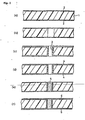
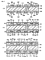
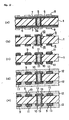
Fig. 1 (a) through (f) are cross-section views illustrating the flow of production of a multilayer printed circuit board in accordance with the first embodiment group of the present invention. -
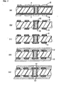
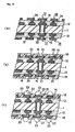
Fig. 2 (a) through (e) are cross-section views illustrating the flow of production of a multilayer printed circuit board in accordance with the first embodiment group of the present invention. -
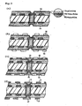
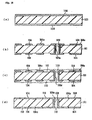
Fig. 3 (a) through (d) are cross-section views illustrating the flow of production of a multilayer printed circuit board in accordance with the first embodiment group of the present invention. -
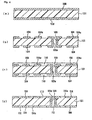
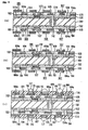
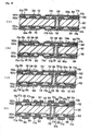
Fig. 4 (a) through (d) are cross-section views illustrating the flow of production of a reference multilayer printed circuit board. -
Fig. 5 (a) through (d) are cross-section views illustrating the flow of production of a reference multilayer printed circuit board. -
Fig. 6 (a) through (d) are cross-section views illustrating the flow of production of a reference multilayer printed circuit board. -
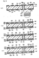
Fig. 7 (a) through (c) are cross-section views illustrating the flow of production of a reference multilayer printed circuit board. -
Fig. 8 (a) through (c) are cross-section views illustrating the flow of production of a reference multilayer printed circuit board. -
Fig. 9 (a) through (d) are cross-section views illustrating the flow of production of a multilayer printed circuit board in accordance with the third embodiment group of the present invention. -
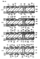
Fig. 10 (a) through (d) are cross-section views illustrating the flow of production of a multilayer printed circuit board in accordance with the third embodiment group of the present invention. -
Fig. 11 (a) through (d) are cross-section views illustrating the flow of production of a multilayer printed circuit board in accordance with the third embodiment group of the present invention. -
Fig. 12 (a) through (c) are cross-section views illustrating the flow of production of a multilayer printed circuit board in accordance with the third embodiment group of the present invention. -
Fig. 13 (a) through (d) are cross-section views illustrating the flow of production of a multilayer printed circuit board in accordance with the third embodiment group of the present invention. -
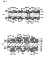
Fig. 14 is a cross-section view showing the manufacture of another multilayer printed circuit board according to the third embodiment group of the present invention. -
Fig. 19 (a) through (f) are cross-section views illustrating the flow of production of a multilayer printed circuit board in accordance with the fifth embodiment group of the present invention. -
Fig. 20 (a) through (e) are cross-section views illustrating the flow of production of a multilayer printed circuit board in accordance with the fifth embodiment group of the present invention. -
Fig. 21 (a) through (d) are cross-section views illustrating the flow of production of a multilayer printed circuit board in accordance with the fifth embodiment group of the present invention. -
Fig. 22 (a) and (b) are cross-section views illustrating the flow of production of a multilayer printed circuit board in accordance with the fifth embodiment group of the present invention. -
Fig. 23 (a) through (f) are cross-section views illustrating the flow of production of a multilayer printed circuit board in accordance with the sixth embodiment group of the present invention. -
Fig. 24 (a) through (e) are cross-section views illustrating the flow of production of a multilayer printed circuit board in accordance with the sixth embodiment group of the present invention. -
Fig. 25 (a) through (d) are cross-section views illustrating the flow of production of a multilayer printed circuit board in accordance with the sixth embodiment group of the present invention. -
Fig. 26 (a) and (b) are cross-section views illustrating the flow of production of a multilayer printed circuit board in accordance with the sixth embodiment group of the present invention. -
Fig. 27 (a) and (b) are cross-section views showing parts of a process for manufacture of a multilayer printed circuit board according to a comparative example pertinent to the sixth embodiment group of the present invention. -
Fig. 28 (a) through (e) are cross-section views showing parts of a process for construction of the conductor circuit according to the seventh embodiment group of the present invention. -
Fig. 29 (a) through (f) are cross-section views illustrating the flow of production of a multilayer printed circuit board in accordance with the seventh embodiment group of the present invention. -
Fig. 30 (a) through (e) are cross-section views illustrating the flow of production of a multilayer printed circuit board in accordance with the seventh embodiment group of the present invention. -
Fig. 31 (a) through (d) are cross-section views illustrating the flow of production of a multilayer printed circuit board in accordance with the seventh embodiment group of the present invention. -
Fig. 32 (a) through (c) are cross-section views illustrating the flow of production of a multilayer printed circuit board in accordance with the seventh embodiment group of the present invention. -
Fig. 37 (a) through (c) are cross-section views illustrating the flow of production of a multilayer printed circuit board in accordance with the eighth group of the present invention. -
Fig. 38 (a) through (d) are cross-section views illustrating the flow of production of a multilayer printed circuit board in accordance with the ninth embodiment group of the present invention. -
Fig. 39 (a) through (d) are cross-section views illustrating the flow of production of a multilayer printed circuit board in accordance with the ninth embodiment group of the present invention. -
Fig. 40 (a) through '(d) are cross-section views illustrating the flow of production of a multilayer printed circuit board in accordance with the ninth embodiment group of the present invention. -
Fig. 41 (a) through (c) are cross-section views illustrating the flow of production of a multilayer printed circuit board in accordance with the ninth embodiment group of the present invention. -
Fig. 42 (a) through (d) are cross-section views illustrating the flow of production of a multilayer printed circuit board in accordance with the ninth embodiment group of the present invention. -
Fig. 43 (a) and (b) are cross-section views illustrating the flow of production of a multilayer printed circuit board in accordance with the ninth embodiment group of the present invention. - The multilayer printed circuit board according to the first embodiment group has a property that a polyolefin resin is used for the resin insulating layer.
- The polyolefin resin mentioned above may be a thermosetting polyolefin resin or a thermoplastic polyolefin resin but is preferably a thermosetting polyolefin resin. This is because, in the process for fabricating a multilayer printed circuit board wherein a plurality of interlayer resin insulating layers are built up in succession, the lower-layer interlayer resin insulating layer, if made of a thermosetting polyolefin resin, will not be deformed upon hot-pressing with the consequent little topological displacement of via holes.
- On the other hand, a thermoplastic polyolefin resin has a high fracture rigidity so that it is able to inhibition of cracks arising from a difference of the coefficient of thermal expansion between the conductor circuit and the resin under the conditions of the heat cycle test.
- The thermoplastic polyolefin resin preferably has a melting point of not less than 200°C. This is because, when the melting point of the resin is not less than 200°C, the deformation upon hot-pressing can be minimized and the melting of the resin insulating layer can be prevented when the multilayer printed circuit board is provided with mounting solder layers or solder vamps by hot-melting at a temperature of not less than 200°C.
- The polyolefin resin to be used in this invention is now described in detail. The polyolefin resin comprises resins having the following structures.
- (1) The resin comprising one and the same repeating unit having the following chemical formula (1):

- (2) The resin comprising a copolymer of two or more different repeating units of the following chemical formula (1):

- (3) The resin containing a different repeating unit of the following chemical formula and having a double bond, an oxide structure, a lactone structure, or a mono- or polycyclopentadiene structure within the backbone chain of its molecule:

- (4) The resin comprising a mixed resin of two or more different resins selected from the above (1), (2) and (3), the rosin comprising a mixed resin of a resin or resins selected from the above (1), (2) and (3) with one or more thermosetting resins, or the resin comprising resins selected from the above (1), (2) and (3) as crosslinked to each other.
- The term "resin" as used in connection with the firs group of the present invention is a collective term covering both a "polymer" and an "oligomer".
- The resins (1) to (3) are first described in detail.
- The reason why the resins (1) to (3) containing the repeating unit structure described above are selected is that the thermosetting polyolefins can be expressed without compromise in fracture rigidity.
- The alkyl group mentioned for X in the above repeating unit structure is preferably at least one member selected from the group consisting of methyl, ethyl, propyl, isopropyl, butyl, isobutyl and t-butyl.
- The unsaturated hydrocarbon residue having 2 to 3 atoms for X in the above repeating unit structure is preferably at least one member selected from the group consisting of CH2=CH-, CH3CH=CH-, CH2=C(CH3)- and acetylene groups.
- The oxide group for X in said repeating unit structure is preferably epoxy and/or propoxy, and the lactone group is preferably at least one member selected from among β-lactone, γ-lactone and δ-lactose groups.
- The reason why said unsaturated hydrocarbon residue having 2 to 3 carbon atoms, oxide group, lactone group, and hydroxyl group are used for X in the repeating unit structure is that those groups are highly reactive so that resins (oligomers) having such functional groups can be easily crosslinked to each other.
- The reason why n is defined as 1 to 10000 is that, if n exceeds 1.0000, the resin will be hardly soluble in solvents and, therefore, difficult to work with.
- Referring to the double bond structure within the backbone chain of said resin (3), a copolymer comprising a repeating unit of the following chemical formula (1) and at repeating unit of the formula -(CH=CH)m- or -(CH2-CH=CH-CH2)m- is preferred.
- In the above formulas, m represents 1 to 10000.

- Referring, further, to said resin (3), the oxide structure in the backbone chain of its molecular is preferably an epoxide. As the lactone structure within the backbone chain, fl-lactone and γ-lactone are preferred. With regard to the mono- or polycyclopentadiene structure within the backbone chain of its molecule, a cyclopentadiene structure or a bicyclopentadiene structure can be selected.
- The copolymer structure mentioned above includes a structure such that the repeating units are copolymerized alternately, e.g. ABAB..., a structure such that the repeating units are copolymerized in a random order, e.g. ABAABAAAAB-, and a structure such that the repeating units are block-copolymerized, e.g. AAAABBB....
- The resin (4) is now described.
- The resin (4) is a polymer alloy comprising a mixed resin of two or more resins selected from said (1), (2) and (3), a polymer alloy comprising a mixed resin of one or more resins selected from said (1), (2) and (3) with a thermosetting resin, or a polymer alloy comprising one or more resins selected from said (1), (2) and (3) as crosslinked to each other.
- The mixed resining of two or more resins selected from said (1), (2) and (3) can be achieved by dissolving the resin particles in an organic solvent or melting them together under heating.
- The blend of one or more resins selected from said categories (1), (2) and (3) with a thermosetting resin is also effected by dissolving the corresponding resin particles in an organic solvent. The preferred thermosetting resin for use in this case is at least one member selected from among thermosetting polyolefin resin, epoxy resin, phenolic resin, polyimide resin and bis(maleimide)triazine resin (BT).
- Furthermore, when resins selected from said (1), (2) and (3) are to be crosslinked to each other, the unsaturated hydrocarbon reside having 2 to 3 carbon atoms, oxide group, lactone group or hydroxyl group and the double bond, oxide structure or lactone structure within the backbone chain of its molecule are utilized as a bonding hand.
- As a representative commercial thermosetting polyolefin resin which can be used in this invention, Sumitomo-3M's product designation 1592 can be mentioned. As commercial thermoplastic polyolefin resins with melting points over 200°C, Mitsui Chemical's product designation TPX (m.p. 290°C) and Idemitsu Petrochemical's product designation SPS (m.p. 270°C) can be mentioned. TPX is a resin corresponding to the case in which X in said repeating unit structure is isobutyl and SPS is a resin containing phenyl for X and having a syndiotactic polymer structure.
- The polyolefin resins described above show high adhesion to conductor circuits so that a conductor circuit can be constructed without roughening the surface of the resin insulating layer. Thus, a conductor circuit can be directly formed on the smooth surface of the resin insulating layer. In particular, by introducing a minor number of polar groups, the adhesion of those polyolefin resins to the conductor circuit can be remarkably improved.
- Furthermore, said polyolefin resins have dielectric constant values not over 3 and dielectric loss tangent values not over 0.005, both being lower than the corresponding values of epoxy resin, with the result that there is no signal delay even when the circuits carry high-frequency signals. Moreover, those polyolefin resins are comparable to epoxy resin in heat resistance so that no stripping of the conductor circuit occurs even at the solder melting temperature. In addition, because of their high fracture rigidity, there is no risk for cracks originating from the interface between the conductor circuit and the resin insulating layer under the conditions of the heat cycle test.
- Preferably, the conductor circuits constituting the multilayer printed circuit board of the invention belonging to the first group are respectively formed on a resin insulating layer by way of a metal layer composed of one or more metals selected from among the metals (exclusive of Cu) of the 4th through 7th periods in Group 4A through Group 1B of the long-form periodic table of the elements, Al and Sn. Such metal layers feature particularly high adhesion to polyolefin resins, insuring very high peel strength values between 1.5 and 2.5 kg/cm.
- The above-mentioned one or more metals selected from among the metals (exclusive of Cu) of the 4th through 7th periods in Group 4A through Group 1B is preferably at least one metal selected from the group consisting of Ni, Co, Cr, Ti and noble metals. The preferred noble metals are Pd, Au and Pt.
- The preferred thickness of this metal layer is 0.01 µm to 0.2 µm. This is because, by selecting a thickness of 0.01 µm or more, a sufficient adhesion can be established between the resin insulating layer and the conductor circuit and by limiting the thickness to 0.2 µm or less, cracks due to a stress of formation of the metal layer by sputtering can be prevented and, at the same time, the unwanted portions of the metal layer between conductor patterns can be easily dissolved and removed by etching after completion of the conductor circuit.
- The above-mentioned metal layer can be formed by various alternative techniques such as electroless plating, electroplating, sputtering, physical vapor deposition and CVD.
- The above-mentioned metal layer composed of one or more metals selected from among the metals (exclusive of Cu) of the 4th through 7th periods in Group 4A through Group 1B, Al and Sn may be formed on the surface of the conductor circuit where necessary. This is because, in the case of a multilayer printed circuit board, an interlayer resin insulating layer must be formed over the conductor circuit and this construction contributes to improved adhesion to the interlayer resin insulating layer.
- Moreover, the multilayer printed circuit board according to the first group of the present invention is preferably a multilayer printed circuit board comprising conductor circuits each formed internally of the substrate board or on the surface thereof.
- The process for manufacturing the printed circuit board according to the first embodiment group of the present invention is now described taking a multilayer printed circuit board as an example.
- (1) First, a circuit board comprising a substrate board and an internal copper pattern formed on the surface thereon is prepared.
The substrate is preferably a member selected from among a glass-epoxy substrate, a polyimide resin substrate, a bis(maleimide)triazine resin substrate, a fluororesin substrate and a polyolefin resin substrate.
For the formation of said copper pattern on the resin substrate, a copper-clad laminate is etched.
Using a drill, through holes are pierced in this substrate and the wall of the through holes and the electroless plating of the surface of the copper foil are performed to provide plated-through holes. The electroless plating is preferably copper electroplating. When the substrate board is one giving a poor plating throwing power as it is the case with a fluororesin substrate, a surface modification pretreatment such as a treatment with a solution of an organometal compound (an organosodium compound) (Tetraetch™, Junkosha) or a plasma treatment is carried out.
Then, electroplating is performed to provide a thick layer. This electroplating is preferably copper electroplating.
The inner walls of the plated-through holes and the surface of the electroplated metal layer may be roughened. This roughening can be carried out by, for example, a blackening (oxidation)-reduction treatment, spraying with an aqueous mixed solution of an organic acid and a cupric complex, or Cu-Ni-P acicular alloy plating.
Where necessary, the plated-through holes may be filled with an electrically conductive paste and a conductor layer be formed over this conductive paste by electroless plating or electroplating. - (2) On the circuit board fabricated in the above step (1), a resin insulating layer composed of a polyolefin resin is constructed. In a multilayer printed circuit board, this resin insulating layer functions as an interlayer resin insulating layer.
This resin insulating layer is formed either by coating with an uncured resin solution or by hot press lamination of a resin film. - (3) Then, this polyolefin resin insulating layer is provided with openings for electrical connection to the lower-layer conductor circuit.
Formation of the openings is carried out with a laser beam. The laser which can be used for this purpose includes a carbon dioxide laser, a UV laser and an eximer laser, among others. When a CO2 laser has been used for piercing the openings, a desmear treatment is performed. This desmear treatment can be carried out using an oxidizing agent such as an aqueous solution of chromic acid or a permanganate or optionally by oxygen plasma treatment, CF4-oxygen mixed plasma treatment or corona discharge treatment. The CF4-oxygen mixed plasma, in particular, is advantageous in that hydrophilic groups such as hydroxyl and carbonyl groups can be introduced into the surface layer of the resin to facilitate the subsequent CVD or PVD treatment. - (4) On the surface of the polyolefin resin insulating layer provided with said openings in the previous step (3), a metal layer composed of at least one metal selected from among said metals (exclusive of Cu) of the 4th through 7th periods in Group 4A through Group 1B, Al and Sn is formed by PVD or CVD method.
PVD method referred to above includes vapor deposition processes such as sputtering and ion beam sputtering. CVD method includes the PE-CVD (plasma enhanced CVD) using an organometal compound (MO), e.g. allylcyclopentadiphenylpalladium, dimethylgold acetylacetate, tin tetramethylacrylonitrile, dicobalt octacarbonylacrylonitrile, etc., as a source. - (5) Then, on the metal layer formed in the above step (4), a metal layer of the same kind of metal as used in the next electroless plating procedure is constructed by sputtering and the like. This metal layer is disposed for the purpose of improving the affinity for the electroless plating metal. Specifically, a copper layer is preferably formed by sputtering.
- (6) Then, electroless plating is applied to the metal layer formed in the above step (5).
The optimum electroless plating is copper plating. The recommended plating thickness is 0.1 to 5 µm. This is because the plated metal layer can be subsequently dissolved and removed by etching without adversely affecting the function of the electroplated conductor layer to be formed in the next step. - (7) Then, a plating resist is disposed on the electroless plated metal layer formed in the above step (6).
This plating resist is formed by laminating a photosensitive dry film and, then, performing a light exposure and development. - (8) Then, using the electroless plated metal film as the plating bar, electroplating is performed to construct a thick conductor circuit. The recommended thickness of this electroplated conductor layer is 5 to 30 µm.
- (9) The plating resist is then stripped off and the electroless plated metal layer underlying the plating resist and said metal layer composed of at least one metal selected from among the metals of the 4th through 7th periods in Group 4A through
Group 18 are dissolved and removed by etching to provide a discrete conductor circuit.
As the etching solution, there can be mentioned an aqueous mixed solution of sulfuric acid and hydrogen peroxide, an aqueous solution of a persulfate such as ammonium persulfate, sodium persulfate, potassium persulfate or the like, an aqueous solution of ferric chloride or cupuric chloride, hydrochloric acid, nitric acid and hot dilute sulfuric acid. - (10) Where necessary, the above sequence of steps (2) to (9) is repeated to provide the objective multilayer printed circuit board.
- While the semi-additive process is used for the formation of a conductor circuit in the above description, the full-additive process may also be adopted.
- The full-additive process mentioned above comprises constructing a thin metal layer on the surface of a polyolefin resin insulating layer by CVD or PVD method, either laminating a photosensitive dry film or coating a liquid photosensitive resin thereon, carrying out a light exposure and development to form a plating resist, and performing an electroless plating to a sufficient thickness to provide a conductor circuit.
- The multilayer printed circuit board according to the second embodiment group of the present invention is a multilayer printed circuit board which comprises a substrate board and, as successively built up on said substrate, a conductor circuit and a resin insulating layer alternately with the conductor circuits being interconnected by via holes, wherein said resin insulating layer comprises a cycloolefin resin.
- In this multilayer printed circuit board according to the second embodiment group of the present invention, because the interlayer resin insulating layer is made of a cycloolefin resin, the dielectric constant and dielectric loss tangent are remarkably small as compared with the interlayer resin insulating layer composed of epoxy resin or the like so that the signal delay and the signal error due to the transmission loss of signals can be prevented.
- Furthermore, because said cycloolefin resin is excellent in mechanical characteristics, particularly, in rigidity, the conductor circuit can be constructed on a firm interlayer resin insulating layer so that the reliability of inter-circuit electrical connection is high.
- In addition, because said cycloolefin resin shows good adhesion to the conductor circuit, the stripping of the interlayer resin insulating layer from the conductor circuit can be prevented and the formation of cracks due to stripping in the interlayer resin insulating layer can also be prevented.
- Furthermore, because said cycloolefin resin has a low water absorption rate, the electrical insulation between conductor circuits can be improved, thus contributing to enhanced reliability.
- The cycloolefin resin mentioned above is not particularly restricted in kind but is preferably a resin having a dielectric constant value at 1 GHz of not more than 3.0 and a dielectric loss tangent value of not more than 0.01. The still more preferred range of dielectric constant is 2.4 to 2.7.
- By using a resin having such a low dielectric constant, the signal transmission delay and error due to the transmission loss of signals can be precluded.
- The preferred cycloolefin resin is a homopolymer or copolymer of 2-norbornene, 5-ethylidene-2-norbornene and/or their derivatives. The derivatives mentioned above include said cycloolefins, e.g. 2-norbornene, to which an amino group, a maleic anhydride residue or a maleic acid-modified group for crosslinking has been attached.
- As the monomer for use in synthesizing said copolymer, there can be mentioned ethylene and propylene.
- The cycloolefin resin mentioned above may be a mixture of two or more species of said resin or even a polymer containing a resin other than said cycloolefin resin.
- Furthermore, when said cycloolefin resin is a copolymer, it may be a block copolymer or a random copolymer.
- The cycloolefin resin mentioned above is preferably a thermosetting cycloolefin resin. This is because, as the resin is crosslinked by heating, its rigidity is increased and mechanical characteristics is also improved.
- The glass transition temperature (Tg) of said cycloolefin resin is preferably 130 to 200°C.
- The cycloolefin resin mentioned above may be used in the form of a resin sheet (film) or may be used in the form of an uncured dispersion of a monomer or a polymer having a curtain low molecular weight in a solvent such as xylene, cyclohexane or the like.
- As the resin sheet, the so-called RCC (RESIN COATED COPPER, i.e. copper foil coated with the resin) can be used.
- The cycloolefin resin need not necessarily contain a filler and other additives or may contain a flame retardant such as aluminum hydroxide, magnesium hydroxide and phosphoric acid esters.
- The process for manufacturing a reference multilayer printed circuit board using such a cycloolefin resin is now described.
- (1) First, a circuit board comprising a resin substrate carrying a lower-layer conductor circuit on its surface is prepared. The resin substrate is preferably a substrate containing an inorganic fiber, such as a glass cloth-epoxy substrate, a glass cloth-polyimide substrate, a glass cloth-bis (maleimide) triazine resin substrate and a glass cloth-fluororesin substrate.
A copper-clad laminate comprising said resin substrate clad with copper foil on both sides can also be used.
Usually, on the resin substrate, through holes are formed with a drill and the electroless plating is carried out on the wall surfaces of the through holes and the surface of the copper foil to provide plated-through holes. The electroless plating is preferably copper plating. In addition, electroplating may be carried out to virtually thicken the copper foil. This electroplating is preferably copper electroplating.
Thereafter, the inner walls of the plated-through holes are roughened and the plated-through holes are filled with a resin paste. Then, an electrically conductive layer is formed over the surface by electroless plating or electroplating.
The roughening treatment may for example be a blackening (oxidation)-reduction treatment, a spray treatment using a mixed aqueous solution of an organic acid and a cupric complex, or a treatment comprising Cu-Ni-P acicular alloy plating.
After the above process, an etching resist is disposed on the solid copper pattern formed all over the substrate using photolithographic technique and, then, etching is performed to construct a lower-layer conductor circuit. Where necessary, the concave area occurred by etching due to the formation of the conductor circuit may be filled with a resin or the like. - (2) The lower-layer conductor circuit thus formed is subjected to a roughening treatment where necessary. The roughening treatment can be carried out by any of the above-mentioned techniques, namely blackening (oxidation)-reduction, spray treatment using a mixed aqueous solution containing an organic acid and a cupric complex, and Cu-NiP acicular alloy plating.
As an alternative, instead of carrying out said roughening of the lower-layer conductor circuit, the substrate board carrying the lower-layer conductor circuit may be dipped in a solution dissolving the resin component to form a resin layer on the surface of said lower-layer conductor circuit for improving the adhesion to the interlayer resin insulating layer to be formed thereon. - (3) Then, an interlayer resin insulating layer composed of said cycloolefin resin is formed on both sides of the circuit board carrying lower-layer conductor circuits as fabricated in the above step (2).
This interlayer resin insulating layer can be formed by coating the substrate with an uncured cycloolefin resin solution and curing the coat by heating or formed by laminating a resin sheet by a press lamination technique under heating and vacuum or reduced pressure. However, the resin sheet laminating technique is preferred from the standpoint of the ease of handling. The heating conditions for use are preferably 100 to 180°C and 0.5 to 20 minutes. - (4) Then, the interlayer resin insulating layer is irradiated with laser light to provide openings for via holes. The laser which can be used includes but is not limited to a carbon dioxide (CO2) laser, a W laser and an eximer layer, although an eximer laser or a CO2 laser of short pulse duration is preferred.
The eximer laser is advantageous in that, with the aid of a mask having through holes corresponding to the openings for via holes, it is capable of piercing many openings for via holes in one operation. The CO2 laser of short pulse duration leaves little residual resin in the openings and does not materially affect the resin around the openings.
The through holes within the mask must be true-round because an exactly circular laser beam spot can be obtained, therefore the diameter of the through holes is preferably about 0.1 to 2 mm.
When openings are pierced with a laser beam, particularly with a CO2 laser beam, a desmear treatment is preferably carried out. This desmear treatment can be carried out using an oxidizing agent comprising an aqueous solution of chromic acid or an aqueous permanganate solution. As an alternative, oxygen plasma, CF4-oxygen mixed plasma, or corona discharge may be utilized for desmear treatment. Surface modification by UV irradiation using a low-pressure mercury vapor lamp may also be performed. - (5) A metal layer may be directly formed on the interlayer resin insulating layer without prior roughening or maybe formed after the surface of the interlayer resin insulating layer has been roughened by plasma treatment or acid treatment.
When a plasma treatment has been performed, an intermediate layer composed of Ni, Ti and/or Pd which has a good adhesion to the interlayer resin insulating layer may be provided to insure a better adhesion between the interlayer resin insulating layer and the upper-layer conductor circuit to be constructed thereon. This intermediate layer of metal mentioned above is preferably formed by a physical vapor deposition (PVD) technique such as sputtering and its thickness is preferably about 0.1 to 2.0 µm. - (6) Following the above step, a thin-film metal layer is formed. The preferred material for this thin film is copper or copper-nickel alloy. This thin-film layer can be formed by physical vapor deposition (PVD), chemical vapor deposition (CVD) or electroless plating.
Specific procedures for said PVD and CVD may be those described for the first group of the present invention.
The preferred thickness of this thin film is 0.1 to 5 µm. This thickness range is chosen because the etching can be carried out without adversely affect the conductor layer to be subsequently formed by electroplating. However, this step of forming a thin film is not essential but may be omitted. - (7) A plating resist is then disposed on the electroless plated metal film formed in the above step (6). This plating resist can be formed by laminating a photosensitive dry film and carrying out a light exposure and development.
- (8) Then, using the thin metal film formed on the interlayer resin insulating layer as a plating bar, electroplating is performed to construct a conductor circuit of sufficient thickness. The preferred thickness of the electroplated metal layer is 5 to 30 µm.
Optionally, the openings for via holes may be filled up by this electroplating to provide the filled via structure. - (9) After this electroplating, the plating resist is stripped off and the electroless plated metal film and intermediate layer mentioned above are dissolved and removed by etching to provide a discrete conductor circuit. The electroplating mentioned above is preferably copper electroplating.
As the etching solution, there can be mentioned an aqueous sulfuric acid-hydrogen peroxide solution, an aqueous solution of a persulfate such as ammonium persulfate, sodiumpersulfate, potassium persulfate or the like, an aqueous solution of ferric chloride or cupric chloride, hydrochloric acid, nitric acid and hot dilute sulfuric acid. Moreover, by using said etching solution comprising an organic acid and a cupric complex, a roughened surface may be formed simultaneously with the etching of the non-conductor circuit regions. - (10) Thereafter, the above sequence of steps (2) to (9) is repeated to provide an upper-layer conductor circuit. Finally, a solder resist layer is formed on the uppermost layer and this solder resist layer is pierced to provided solder vamps, whereby a multilayer printed circuit board comprising, for examples, 3 layers on either side, thus 6 layers in both sides is obtained.
- The multilayer printed circuit board according to the fifth embodiment group of the present invention comprises a resin insulating layer and the corresponding conductor circuit as built up on both sides of the substrate boards and further comprises a metal layer composed of at least one metal selected from among metals (exclusive of Cu) of the 4th through 7th periods in Group 4A to Group 1B of the periodic table of the elements, Al and Sn as formed on the surface of said resin insulating layer and an upper-layer conductor circuit as constructed further on said metal layer.
- Since the metal constituting said metal layer has a high adhesion to the insulating resin, the resin insulating layer can obtain a firm adhesion to the upper-layer conductor circuit without providing a roughened layer on the surface thereof. As a result, the resin insulating layer presents with a flat and level surface and the surface of the conductor circuit also becomes flat so that no signal conduction delay occurs even when high-frequency signals are used.
- Unlike a ceramic substrate and a metal substrate, a resin substrate is liable to undergo warpage and so poor in heat radiation that a migration of copper ions due to heat accumulation tends to take place. However, the above-mentioned transition metal constituting said metal layer according to this invention is harder than copper and the metal layer composed of such a metal inhibits expansion and shrinkage of the interlayer resin insulating layer. Moreover, because such a metal layer is constructed on both sides of the resin substrate, the warping and cracking of the substrate board under the condition of the heat cycle test can be prevented and, in addition, this metal layer serves as a barrier to the migration of copper ions from the copper conductor circuit, thus promising an effective layer to layer insulation even in a highly humid environment.
- Moreover, a Cu layer may be disposed on said transition metal film. When the conductor circuit to be formed thereon is of copper, such a Cu layer improves the adhesion between the transition metal and the conductor circuit.
- In the multilayer printed circuit board according to the fifth group of the present invention, the metal constituting said metal layer is at least one transition metal selected from among Al, Fe, W, Mo, Sn, Ni, Co, Cr, Ti and noble metals. The preferred noble metals are Pd, Au and Pt.
- The thickness of the metal layer composed of said transition metal is preferably 0.02 µm to 0.2 µm. The reason is as follows. When the thickness is not less than 0.02 µ m, a good adhesion can be established between the resin insulating layer and the conductor circuit. On the other hand, when the thickness is not over 0.2 µm, cracking due to the stress applied in the formation of the metal layer by a sputtering technique can be prevented and, moreover, the metal layer among the conductor circuits which has become unnecessary after construction of the conductor circuit can be easily dissolved and removed by etching.
- The thickness of the Cu layer to be formed on said transition metal layer is preferably 0.02 to 0.2 µm. Thus, when the thickness is not less than 0.02 µm, a good adhesion can be obtained between the transition metal layer and the conductor circuit. On the other hand, when the thickness is not more than 0.2 µm, cracking due to the stress applied in the formation of the metal layer by a sputtering technique can be prevented and, moreover, the Cu layer among the conductor circuits which has become unnecessary after construction of the conductor circuit can be easily dissolved and removed by etching.
- On the above metal layer, a metal layer of a different sort is preferably provided as necessary. More particularly, when a nickel layer is first formed on the resin insulating layer and a copper layer is then formed in superimposition, the incidence of bare spots in the construction of a conductor circuit can be prevented.
- The metal layer mentioned above is formed by electroless plating, electroplating, sputtering, physical vapor deposition or CVD.
- Unlike the ceramic substrate and metal substrate, the resin substrate for use in the fifth group of the present invention is generally liable to undergo warping and, moreover, poor in heat radiation efficiency so that the migration of copper ions due to heat accumulation tends to take place . In this respect, according to this fifth group of the invention, metal layer serves as a barrier to the migration of copper ions from the copper conductor circuit, thus insuring a good layer to layer insulation even in a highly humid environment.
- The interlayer resin insulating layer in the fifth group of the present invention is preferably formed from a thermosetting resin, a thermoplastic resin or a mixed resin thereof.
- The preferred thermosetting resin is at least one member selected from the group consisting of thermosetting polyolefin resin, epoxy resin, polyimide resin, phenolic resin and bis(maleimide)triazine resin.
- The preferred thermoplastic resin is at least one member selected from among engineering plastics such as polymethylpentene (PMP), polystyrene (PS), polyethersulfone (PES), polyphenylene ether (PPE), polyphenylene sulfide (PPS), etc.
- In the fifth embodiment group of the present invention, said interlayer resin insulating layer is most preferably formed from the same polyolefin resin as mentioned for the first group of the present invention.
- The polyolefin resins described above show high adhesion to conductor circuits so that a conductor circuit can be constructed without roughening the surface of the resin insulating layer. Thus, a conductor circuit can be directly formed on the surface of the smooth resin insulating layer.
- Furthermore said polyolefin resins have dielectric constant values not more that 3 and dielectric loss tangent values not more than 0.05, both being lower than the corresponding values of epoxy resin, with the result that there is no signal conduction delay even when high-frequency signals are carried. Moreover, those polyolefin resins are comparable to epoxy resin in heat resistance so that no stripping of the conductor circuit occurs even at the solder melting temperature. In addition, because of their high fracture rigidity, there is no risk for cracks originating from the interface between the conductor circuit and the resin insulating layer under the conditions of the heat cycle test.
- An exemplary process for manufacturing a multilayer printed circuit board according to the fifth embodiment group of the present invention is now described.
- (1) First, a circuit board comprising a resin substrate board and, as disposed on the surface thereof, an inner copper pattern is prepared.
For this preparation, the same procedure as described for the first embodiment group of the invention can be used. - (2) Then, a resin insulting layer is formed on both sides of the circuit board as prepared in the above step (1). This resin insulating layer functions as an interlayer resin insulating layer of the multilayer printed circuit board.
This resin insulating layer can be provided either by coating with an uncured resin solution or by hot-press lamination of a resin film. - (3) Then, the resin insulating layer thus formed is provided with openings in order to ensure electrical connection to the lower-layer conductor circuit.
Formation of the openings is performed by irradiation with laser light. The laser which can be used includes but is not limited to the CO2 laser, UV laser and eximer laser. When a CO2 laser is used for the formation of said openings, desmear treatment is performed as an after-treatment. This desmear treatment can be carried out using an oxidizing agent comprising an aqueous solution of chromic acid or an aqueous permanganate solution. A treatment with oxygen plasma, CF4-oxygen mixed plasma or corona discharge can also be used. Surface modification by UV irradiation using a low-pressure mercury-vapor lamp is also useful.
Particularly the CF4-oxygen mixed plasma treatment is advantageous in that hydrophilic groups such as hydroxy and carbonyl groups can be introduced onto the resin surface and, hence, the subsequent CVD or PVD treatment will be facilitated. - (4) On the surface of the resin insulating layer formed with openings in the above step (3), a thin metal layer composed of at least one metal selected from among metals of the 4th through 7th periods in Group 4A through Group 1B is formed by, for example, a plating, PVD or CVD technique.
Specific procedures for PVD and CVD may be those described hereinbefore for the first embodiment group of the present invention. - (5) Then, on the metal layer formed in the above step (4), another metal layer similar to the electroless plated metal layer to be formed in the next step is formed by, for example, sputtering. This procedure is intended to improve the affinity for the electroless plated metal layer. More particularly, a copper layer is preferably formed by sputtering.
- (6) The metal layer formed in the above step (5) is further electroless plated.
The optimum kind of electroless plating is copper plating. The preferred thickness of electroless plating is 0.1 to 5 µ m. This thickness range is selected because the layer can be dissolved and removed by etching without adversely affecting the function of the electroplated conductor layer to be subsequently constructed. - (7) A plating resist is then disposed on the electroless plated layer formed in the above step (6). This plating resist can be formed by laminating a photosensitive dry film and carrying out the light exposure and development.
- (8) Then, using the electroless plated film as a plating bar, electroplating is performed to provide a conductor circuit in a sufficient thickness. The preferred thickness of this electrolated metal layer is 5 to 30 µm.
- (9) Then, the plating resist is stripped off and the electroless plated film and said metal layer composed of at least one metal selected from among metals of the 4th through 7th periods in Group 4A through Group 1B under the plating resist are dissolved and removed by etching to provide a discrete conductor circuit.
The etching solution which can be used includes but is not limited to an aqueous sulfuric acid-hydrogen peroxide solution, an aqueous solution of a persulfate, e.g. ammonium persulfate, sodium persulfate, potassium persulfate or the like, an aqueous solution of ferric chloride or cupric chloride, hydrochloric acid, nitric acid and hot dilute sulfuric acid. - (10) Where necessary, on the surface of the conductor circuit, a thin metal layer composed of at least one metal selected from among metals of the 4th through 7th periods in Group 4A to Group 1B of the long-form periodic table (exclusive of Cu), Al and Sn is formed by plating, PVD or CVD and the above sequence of steps (2) to (9) is repeated to provide a multilayered printed circuit board.
- While the above description pertains to the construction of a conductor circuit by the semi-additive process, the full-additive process may be likewise employed.
- This full-additive process comprises forming a thin metal layer on the surface of a resin insulating layer by CVD or PVD, laminating a photosensitive dry film or coating a liquid photosensitive resin; carrying out light exposure and development to dispose a plating resist and carrying out electroless plating to a sufficient thickness to provide a conductor circuit.
- As an alternative, a conductor circuit can be constructed by disposing a plating resist on the surface of a resin insulating layer, forming a thin metal layer by a CVD or PVD technique, sanding off this metal layer adherent to the surface of the plating resist or removing the plating resist itself and, using this metal layer as catalyst, performing electroless plating.
- The multilayer printed circuit board according to the six embodiment group of the present invention comprises a metal layer composed of at least one metal selected from among metals (exclusive of Cu) of the 4th through 7th periods in Group 4A to Group 1B of the long-form periodic table of the elements, Al and Sn is disposed on at least part of the surface of the lower-layer conductor circuit formed on both sides of a resin substrate board.
- The metal mentioned above is preferably selected from among Al, Fe, W, Mo, Sn, Ni, Co, Cr, Ti and noble metals, and the preferred noble metals are Pd, Au and Pt.
- All the above metals provide good adhesion to the interlayer insulating resin. Therefore, even when warpage occurs in the resin substrate, no delamination is induced between the conductor circuit and the interlayer resin insulating layer. Moreover, since such structures as above are formed symmetrically on both sides of the resin substrate, the amount of warpage of the substrate itself is decreased to prevent cracking which might occur around the interface between the conductor circuit and the interlayer resin insulating slayer even when it undergoes the heat cycle tests.
- Furthermore, when a metal layer composed of the above-mentioned metal is formed, the required degree of adhesion to the upper-layer conductor circuit can be insured even without roughening the surface of the conductor circuit, with the result that no conduction delay occurs even when high-frequency signals are carried.
- When the conductor circuit is formed by etching, said metal layer acts as an etching resist, thus contributing to the formation of a fine pattern.
- The thickness of the metal layer mentioned above is preferably 0.01 µm to 0.2 µm. The reason is as follows. When the thickness is not less than 0.01 µm, a good adhesion can be obtained between the resin insulating layer and the conductor circuit. On the other hand, when the thickness is not over 0.2 µm, cracking due to the stress of formation of the metal layer by sputtering can be prevented and, moreover, the metal layer among the conductor circuits which has become unnecessary after construction of the conductor circuit can be easily dissolved and removed by etching.
- On the above metal layer, a metal layer composed of a different kind of metal may be provided as necessary. More particularly, when a nickel layer is first formed on the interlayer resin insulating layer and a copper layer is then formed in superimposition, the incidence of bare spots in the construction of a conductor circuit can be prevented. The metal layer mentioned above is formed by electroless plating, electroplating, sputtering, vapor deposition or CVD.
- Unlike the ceramic substrate or the metal substrate, the resin substrate for use in the sixth group of the present invention is generally liable to undergo warping and, moreover, poor in heat radiation factor so that the migration of copper ions due to heat accumulation tends to take place. In this respect, the metal layer in this invention serves as a barrier to the migration of copper ions from the copper conductor circuit, thus insuring a good layer to layer insulation even in a highly humid environment.
- The interlayer resin insulating layer in the sixth group of the present invention is preferably formed from a thermosetting resin, a thermoplastic resin or a mixed resin thereof.
- The preferred thermosetting resin is at least one member selected from the group consisting of thermosetting polyolefin resin, epoxy resin, polyimide resin, phenolic resin and bis(maleimide)triazine resin.
- The preferred thermoplastic resin is at least one member selected from among the so-called engineering plastics such as polymethylpentene (PMP), polystyrene (PS), polyethersulfone (peps), polyphenylene ether (PPE), polyphenylene sulfide (PPS), etc.
- In this invention, said interlayer resin insulating layer is most preferably formed from the same polyolefin resin as mentioned for the first embodiment group of the present invention.
- The polyolefin resin mentioned above provides for good adhesion to the conductor circuit even without roughening the surface of the inner-layer conductor circuit so that a flat and level conductor circuit can be provided.
- Furthermore, said polyolefin resins have dielectric constant values not less than 3 and dielectric loss tangent values not more than 0.05, both being lower than the corresponding values of epoxy resin, with the result that there is no signal conduction delay even when high-frequency signals are used. Moreover, those polyolefin resins are comparable to epoxy resin in heat resistance so that no stripping of the conductor circuit occurs even at the solder melting temperature. In addition, because of their high fracture rigidity, there is no risk for cracks originating from the interface between the conductor circuit and the resin insulating layer under the conditions of the heat cycle test.
- An exemplary process for manufacturing a multilayer printed circuit board according to the sixth embodiment group of the present invention is now described.
- (1) First, a circuit board comprising a resin substrate board and, as disposed on the surface thereof, an inner-layer cropper pattern is prepared.
For this preparation, the same procedure as described for the first and second groups of the present invention can be used. - (2) Then, a resin insulating layer is formed on both sides of the circuit board as prepared in the above step (1). This resin insulating layer functions as an interlayer resin insulating layer of the multilayer printed circuit board.
This resin insulating layer can be provided either by coating with an uncured resin solution or by hot-press lamination of a resin film. - (3) Then, the resin insulating layer thus formed is provided with openings to insure an electrical connection to the lower-layer conductor circuit.
Formation of said openings is performed by irradiation with laser light. The laser which can be used includes but is not limited to the CO2 laser, UV laser and eximer laser. When a CO2 laser is used for the formation of said openings, desmear treatment is performed as an after-treatment. This desmear treatment can be carried out using an oxidizing agent comprising an aqueous solution of chromic acid or an aqueous permanganate solution. A treatment with oxygen plasma, CF4-oxygen mixed plasma or corona discharge can also be used. Surface modification by UV irradiation using a low-pressure' mercury-vapor lamp is also usable.
Particularly the CF4-oxygen mixed plasma treatment is advantageous in that hydrophilic groups such as hydroxyl and carbonyl groups can be introduced onto the resin surface and, hence, the subsequent CVD or PVD treatment will be easy to handle. - (4) On the surface of the resin insulating layer formed with openings in the above step (3), a thin metal layer composed of at least one metal selected from among metals (exclusive of Cu) of the 4th through 7th periods in Group 4A through Group 1B, Al and Sn is formed by, for example, a plating, PVD or CVD technique.
Specific procedures of PVD and CVD may be those described hereinbefore for the first group of the present invention. - (5) Then, on the metal layer formed in the above step (4), a metal layer similar to the electroless plated layer to be formed in the next step is formed by, for example, sputtering. This procedure is intended to improve the affinity for the electroless plated metal layer. More particularly, a copper layer is preferably formed by sputtering.
- (6) Electroless plating is performed on the metal layer formed in the above step (5).
The optimum kind of electroless plating is copper plating. The preferred electroless plating thickness is 0.1 to 5 µm. This thickness range is selected because the layer can be dissolved and removed by etching without adversely affecting the function of the electroplated conductor layer to be subsequently constructed.
This electroless plated metal layer and/or the said thin metal layer composed of at least one metal selected from among metals (exclusive of Cu) of the 4th through 7th periods in Group 4A to Group 1B, Al and Sn serves as plating bar. - (7) A plating resist is disposed on the electroless plated metal layer formed in the above step (6). This plating resist is formed by laminating a photosensitive dry film and carrying out the light exposure and development.
- (8) On the electroless plated metal layer subjected to the procedure described in the above step (7), a metal layer composed of at least one metal selected from among metals (exclusive of Cu) of the 4th through 7th periods in Group 4A to Group 1B, Al and Sn is formed by said plating, PVD or CVD technique.
It is particularly preferable that the formation of said metal layer in this step be carried out by electroless plating.
Then, using said electroless plated metal layer and said metal layer as the plating bar, electroplating is performed to provide a conductor circuit in a sufficient thickness. The thickness of the electroplated metal layer formed by this treatment is preferably 5 to 30 µm. - (9) Then, said plating resist is stripped off and the electroless plated metal film and said metal layer under the plating resist are dissolved and removed by etching to provide a discrete conductor circuit. The etching solution which can be used in this step includes but is not limited to an aqueous sulfuric acid-hydrogen peroxide solution, an aqueous solution of a persulfate, e.g. ammonium persulfate, sodium persulfate, potassium persulfate or the like, an aqueous solution of ferric chloride or cupric chloride, hydrochloric acid, nitric acid and hot dilute sulfuric acid.
In this etching treatment, said metal layer serves as an etching resist so that even a discrete conductor circuit with an L/S value of 15/15 µm (L/S means line/space) can be provided. - (10) Where necessary, on the surface of said conductor circuit, a thin metal layer composed of said metal is formed by plating, PVD or CVD and the above sequence of steps (2) to (9) is repeated to provide a double-sided multilayered printed circuit board.
- While the above description pertains to the construction of conductor circuits by the semi-additive process, the full-additive process may be likewise employed.
- This full-additive process comprises forming a thin metal layer on the surface of a resin insulating layer by CVD or PVD, laminating a photosensitive dry film or coating a liquid photosensitive resin, carrying out light exposure and development to dispose a plating resist and carrying out electroless plating to a sufficient thickness to provide a conductor circuit.
- As an alternative, a conductor circuit can be constructed by disposing a plating resist on the surface of a resin insulating layer, forming a thin metal layer by a CVD or PVD technique, removing by abrasion or the like this metal layer adherent to the surface of the plating resist or stripping off the plating resist itself and, using this metal layer as catalyst, performing electroless plating.
- The process for fabricating a conductor circuit according to the first embodiment of the seventh group of the present invention comprises at least the following steps (1) through (3), namely (1) a step of forming a first conductor layer composed of a metal forming a passivation film on the surface thereof, such as Ni or Al; on an insulating substrate board, (2) a step of forming a second conductor layer composed of a metal having the ionization tendency lower than said metal forming a passivation film on surface, such as Ni or Al, on said first conductor layer and (3) performing selective etching with an acid etching solution to simultaneously etching said first conductor layer and second conductor layer in specified regions.
- In the above process for fabricating a conductor circuit, etching results in dissolution of the metal having the ionization tendency lower than the metal forming a passivation film on surface in the first place so that the metal forming a passivation film on surface, such as Ni or Al, is exposed on the surface. As the metal forming a passivation film on surface, such as Ni or Al, is thus exposed on the surface, this metal and the metal having a lower ionization tendency undergo a cell reaction with the acid etching solution acting as electrolyte, with the result that the metal forming a passivation film, e.g. Ni or al, is dissolved.
- Therefore, said acid etching solution may be an aqueous solution of sulfuric acid, an aqueous solution of hydrogen chloride or a mixed aqueous sulfuric acid-hydrogen peroxide solution and it is not necessary to use an acid not suited for a high-production run, such as aqua regia or nitric acid.
- Furthermore, the use of said acid etching solution contributes to a higher etching rate than ever before.
- In the embodiment of the seventh group, the metal forming a passivation film on surface is preferably at least one metal selected from among Ni, Co, Cr, Ti, Nb, Ta and Al.
- This is because those are ready to form a passivation film and not soluble in the ordinary acid etching solution.
- The particularly preferred metal forming a passivation film on surface includes Ni and Al, for those metals show good adhesion to resins and are most suited for use for constructing the conductor circuit of the printed circuit board.
- This embodiment is now described in further detail, reference being had to the accompanying drawings. The following description is pertinent to the case in which Ni or Al is used as said metal forming a passivation film on surface.
-
Fig. 28 (a) to (e) are schematic cross-section views showing the steps constituting the process for constructing a conductor circuit in accordance with this embodiment. - In the seventh group of the present invention, a
first conductor layer 32 composed of Ni or Al is formed on an insulatingsubstrate board 31 in the first place [Fig. 28(a) ]. - The material for said insulating
substrate board 31 is not particularly restricted but includes substrate boards made of inorganic materials, such as ceramic boards, and substrate boards made of organic materials, such as resin boards. However, this embodiment is chiefly directed to the use of a resin substrate because the embodiment provides for a conductor layer with good adhesion to a resin board when it is poor in the adhesion to a conductor layer formed. - The technique of forming said
first conductor layer 32 is not particularly restricted but includes vapor deposition techniques and plating, among others. However, vapor deposition, particularly sputtering, is preferred because it is conducive to formation of a conductor layer showing good adhesion to a resin substrate. When thefirst conductor layer 32 is to be constructed by sputtering, the procedure is preferably carried out in an inert gas atmosphere under reduced pressure so that thefirst conductor layer 32 once formed will not be oxidized. - Then, on the
first conductor layer 32 formed on said insulatingsubstrate board 31, asecond conductor layer 33 composed of a metal having the ionization tendency lower than Ni or Al is constructed. [Fig. 28 (b) ]. - The metal having the ionization tendency lower than Ni includes but is not limited to Cu, Sn and Pb. Those metals may be used each alone or in combination. Thus, a layer composed exclusively of such a metal may be formed or alternatively a plurality of layers of such metals may be disposed.
- The metal having the ionization tendency lower than Al includes but is not limited to Cu, Sn, Pb and Fe. Those metals may also be used each alone or in combination.
- The technique of forming the
second conductor layer 33 is not particularly restricted, either, but includes vapor deposition and plating, among others. However, the use of the same technique as used above faciliates the construction of a conductor layer. Thus, it is preferable to use the same technique as used in the construction of thefirst conductor layer 32. In other words, both thefirst conductor layer 32 and thesecond conductor layer 33 are constructed by the same vapor deposition technique, such as sputtering. - In order that the
first conductor layer 32 will not be oxidized in the formation of thesecond conductor layer 33, the latter layer is preferably constructed as quickly as possible after construction of theformer layer 32 avoiding exposure of thelayer 32 to atmospheric air. - After the construction of the
second conductor layer 33, selective etching is performed with an acid etching solution to simultaneously etching thefirst conductor layer 32 andsecond conductor layer 33 in specified regions to construct a conductor circuit. - The method for selective etching is not particularly restricted but may, for example, comprise disposing an etching resist on the above two-component conductor layer and etching the regions not covered with the etching resist to provide a conductor circuit. An alternative method may comprise disposing a plating resist, thickening the conductor layer not covered with the plating resist by, for example, electroplating, stripping off the plating resist and etching the conductor layer under the plating resist to provide a conductor circuit.
- In the following description, the former method is employed. The latter method will be described in detail in connection with the process for manufacturing a printed circuit board.
- Thus, using a photolithographic technique, an etching resist 34 is constructed on the
second conductor layer 33 in the first place [Fig. 28 (c) ]. Then, the region not covered with the etching resist 34 is dissolved and removed by etching to provide a conductor circuit. - This etching treatment can be carried out using an acid etching solution.
- The acid etching solution mentioned just above includes easily-manageable etching solutions which are generally used, for example an aqueous solution of sulfuric acid, an aqueous solution of hydrogen chloride or a mixed aqueous sulfuric acid-hydrogen peroxide system.
- Assuming that the
first conductor layer 32 is an Ni layer, thesecond conductor layer 33 is a Cu layer, and the etching solution is an aqueous sulfuric acid-hydrogen peroxide system, etching proceeds in the following manner. - First, according to the following chemical formulas (1) and (2), the Cu layer is dissolved and removed by etching.
Cu+H2O2→CuO+H2O (1)
CuO+H2SO4→Cu2++SO4 2-+H2O (2)
- As the Cu layer is dissolved and removed by etching to expose the Ni layer, the etching of Ni layer begins.
- When the layer composed exclusively of Ni is etched, the reaction may proceed according to the following chemical formulas (3) and (4).
Ni+H2O2-+NiO+H2O (3)
NiO+H2SO4→Ni2++SO4 2-+H2O (4)
- Actually, however, the reaction between the NiO originating from the above formula (3) and H2SO4, that is to say the reaction according to the formula (4), does not proceed appreciably so that the Ni layer is covered with an oxide film and, therefore, substantially not etched.
- On the other hand, in the present invention wherein the conductor layer has a binary structure composed of a Cu layer and a Ni layer, an electric cell is formed by the Cu layer as cathode and the Ni layer as anode, with the result that the reactions according to the following formulas (5) and (6) take place and proceed.
Cu2+→Cu (5)
Ni→Ni2+ (6)
- As to Cu, the oxidation reaction (ionization reaction) due to said etching and the reduction reaction due to the cell formed as above proceed reversibly but because the ionization tendency of Ni is higher than that of Cu, only the irreversible reaction from Ni metal to Ni ion proceeds so that Ni dissolves in the solution and etching is proceeded. Moreover, since this reaction does not involve formation of an oxide, it does not happen that Ni is passivated to stop the reaction but the reaction proceeds to an end for complete etching [
Fig. 28 (d) ]. - Then, the etching resist is stripped off, whereupon a conductor circuit comprising the
first conductor layer 32 andsecond conductor layer 33 is obtained on the insulating substrate board 31 [Fig. 28(e) ]. - Since, in the process for constructing a conductor circuit according to the seventh embodiment group of the present invention, the
second conductor layer 33 composed of a metal having the ionization tendency lower than Ni or Al is formed on thefirst conductor layer 32 composed of Ni or Al so that said selective etching can be easily carried out using an easily manageable acid solution such as an aqueous solution of hydrogen chloride. Moreover, as the first conductor layer 32.of Ni or Al is first formed on the insulatingsubstrate board 31, a flat and level conductor circuit with good adhesion to the substrate can be formed particularly when the insulatingboard 31 is a resin board. - The process for manufacturing a multilayer printed circuit board according to the second invention belonging to the seventh group of the present invention is now described.
- In this process for manufacturing a multilayer printed circuit board according to the second embodiment of the seventh group, a resin insulating layer and a conductor circuit are built up in succession on an insulating substrate board, which comprises at least the following steps [1] to [5], namely [1] a step of forming a first conductor layer composed of a metal forming a passivation film on surface, such as Ni or Al, on a resin insulating layer, [2] a step of foxing a second conductor layer composed of a metal having the ionization tendency lower than said metal forming a passivation film on surface, such as Ni or Al, on said first conductor layer, [3] a step of disposing a plating resist on said second conductor layer, (4) a step of forming a third conductor layer by electroplating on said second conductor layer carrying said plating resist and [5] a step of striping off the plating resist and, using an acid etching solution, etching the first conductor layer and second conductor layer under said plating resist simultaneously.
- The metal having the ionization tendency lower than said metal forming a passivation film on surface and the acid etching solution, which are for use in the process for manufacturing a multilayer printed circuit board according to the second invention belonging to the seventh group of the present invention, may be quite the same metal and etching solution as mentioned for the above-described process for constructing a conductor circuit.
- Furthermore, etching in the above step (5) proceeds according to the same reactions as mentioned above for the process for constructing a conductor circuit, and the first conductor layer and second conductor layer under the plating resist are simultaneously dissolved and removed by etching.
- The process for manufacturing a multilayer printed circuit board according to the second invention of the seventh group may be carried out by using a resin substrate on which a conductor circuit has been directly formed and building up a resin insulting layer and a conductor circuit in that order each in a single layer or in a plurality of layers over the first-mentioned conductor circuit. As an alternative, it is possible to use a resin substrate not formed with a conductor circuit and construct a resin insulating layer and a conductor circuit in that order each in a single layer or in a plurality of layers. Moreover, said resin insulating layer and said conductor circuit may be built up only on one side of the resin substrate board or on both sides.
- A typical procedure for carrying out the process for manufacturing a multilayer printed circuit board according to the second embodiment of the seventh group is now described in detail.
- (1) First, a circuit board comprising a resin substrate board and, as formed on the surface thereof, a lower-layer conductor circuit (inner copper pattern) is provided.
This fabrication of the circuit board can be carried out by the same procedure as described for the embodiment of the first group. - (2) Then, a resin insulating layer is formed on both sides of the circuit board prepared in the above step (1). This resin insulating layer functions as an interlayer resin insulating layer of the multilayer printed circuit board.
Preferably this resin insulating layer is composed of a thermosetting resin, a thermoplastic resin or a mixed resin thereof.
The preferred thermosetting resin is preferably one member selected from the group consisting of thermosetting polyolefin resins, epoxy resins, polyimide resins, phenolic resins and bis(maleimide)triazine resins.
The preferred thermoplastic resin is preferably selected from among engineering plastics such as polymethylpentene (PMP), polystyrene (PS), polyethersulfone (PES), polyphenylene ether (PPE), polyphenylene sulfide (PPS), etc. - (3) Then, this resin insulating layer (hereinafter referred to as the interlayer resin insulating layer) is provided with openings for via holes for securing an electrical connection to the lower-layer conductor circuit.
When a photosensitive resin is used, said openings for via holes are pierced in the above-mentioned interlayer resin insulating layer by light exposure and development and thermal curing. When a thermosetting resin or a polyolefin resin is used, said openings are pierced by means of laser light.
The laser for use in this laser processing includes but is not limited to the carbon dioxide gas laser, ultraviolet laser and eximer laser. - (4) Then, as the above-mentioned step [1], a first conductor layer composed of a metal forming a passivation film on surface, e.g. Ni or Al, is formed on the resin insulating layer.
The technique of forming this first conductor layer is not particularly restricted but sputtering in an inert gas atmosphere under reduced pressure is preferred. The preferred thickness of said first conductor layer is 0.01 to 0.5 µm.
In this manner, a flat and level first conductor layer showing good adhesion to the resin insulating layer can be constructed on said resin insulating layer. - (5) Then, as said step [2], a second conductor layer composed of a metal having the ionization tendency lower than said metal forming a passivation film on surface, such as Ni or Al, is formed on said first conductor layer.
The technique of forming this second conductor layer is not particularly restricted, either, but sputtering in an inert gas atmosphere under reduced pressure is preferred. The preferred thickness of said second conductor layer is 0.05 to 1.0 µm. - (6) As said step (3), a plating resist is disposed on the second conductor layer formed in the above step (5).
The technique of disposing said plating resist is not particularly restricted but generally the resist is formed by laminating a photosensitive dry film and carrying out light exposure and development. - (7) Then, as said step (4), a third conductor layer is formed by electroplating using the electroless plated layer as a plating bar to thicken the conductor circuit. The preferred thickness of this third conductor layer (electroplated copper layer) is 5 to 30 µm.
- (8) After completion of the third conductor layer, said step (5) is carried out. Thus, the plating resist is stripped off and the second conductor layer and first conductor layer beneath the plating resist are dissolved and removed by etching with an acid etching solution to provide a discrete conductor circuit.
The acid etching solution that can be used for this purpose includes easily manageable acid solutions such as an aqueous solution of sulfuric acid, an aqueous solution of hydrogen chloride and a mixed aqueous solution of sulfuric acid and hydrogen peroxide. - (9) Where necessary, an Ni layer is formed on the surface of the conductor circuit by plating, physical vapor deposition (PVD) or chemical vapor deposition (CVD) and, then, the above sequence of steps (2) to (8) is repeated to provide a multilayer printed circuit board.
-
(1) A copper-clad BT resin laminate (Mitsubishi Gas Chemical; product designation: HL 830-C, 8T12D) comprising a 0.8 mm-thick BT [bis(maleimide)triazine]resin substrate 1 and an 18 µ m-thick copper foil 2 laminated to both sides thereof was used as the starting material [Fig. 1(a) ]. First, this copper-clad laminate was drilled [Fig. 1(b) ] and a palladium-tin coloid was applied. Using an aqueous electroless plating solution of the under-mentioned formulation, electroless plating was performed to form a 0.7 µm-thick electroless plated copper film on the entire substrate surface.[Aqueous electroless plating solution] EDTA 150 g/L Copper sulfate 20 g/L HCHO 30 ml/L NaOH 40 g/L α,α'-Bipyridyl 80 mg/L PEG 0.1 g/L [Electroless plating conditions] Bath temperature: 70°C, for 30 min.
Then, using an aqueous electroplating solution of the under-mentioned formulation, copper electroplating was performed to provide a 15 µm-thick copper electrodeposition film [Fig. 1(c) ].[Aqueous electroplating solution] Sulfuric acid 180 g/L Copper sulfate 80 g/L Additive (Atotech Japan, product designation: Kaparacid GL) 1 ml/L [Electroplating conditions] Current density 1A/dm2 Time 30 min. Temperature Room temperature
(2) The substrate board carrying an inner copper pattern thus formed (inclusive of plated-through holes 3) was rinsed with water and dried. Then, using an aqueous solution containing NaOH (20 g/L), NaClO2 (50 g/L) and Na3PO4 (15.0 g/L) as oxidation bath (blackening bath) and an aqueous solution containing NaOH (2.7 g/L) and NaBH4 (1.0 g/L) as reduction bath, an oxidation-reduction treatment was carried out to provide a roughenedlayer 4 on the entire surface of the conductor circuit and plated-through holes [Fig. 1(d) ].
(3) The plated-throughholes 3 were then filled with an electricallyconductive paste 5 containing copper particles by a screen-printing technique and the paste was then dried and cured. The roughenedlayer 4 on the conductor and the excessconductive paste 5 exposed from the plated-throughholes 3 were removed by sanding with a belt sander using a #400 belt sanding paper (Sankyo Rikagaku), followed by abrasion to remove the injuries caused by sanding to flatten the substrate board surface [Fig. 1(e) ].
(4) To the flattened surface of the substrate board as prepared in the above step (3) was applied a colloidal palladium catalyst, and electroless plating was carried out in the routine manner to form a 0.6 µm-thick electroless plated copper film 6 [Fig. 1(f) ].
(5) Then, copper electroplating was performed under the following conditions to form aelectroplating copper layer 7 in a thickness of 15 for thickening the part which was to become aconductor circuit 9 and a conductor layer (cover plating layer) 10 to cover theconductive paste 5 filled into the plated-through holes 3.[Aqueous electroplating solution] Sulfuric acid 180 g/L Copper sulfate 80 g/L Additive (Atotech Japan, product designation: Kaparacid GL) 1 ml/L [Electroplating conditions] Current density 1A/dm2 Time 30 min. Temperature Room temperature
(6) To both sides of the substrate board thus formed with said laver to become theconductor circuit 9 andconductor layer 10, a commercial photosensitive dry film was laminated, and with a mask set in position, light exposure at 100 mJ/cm2 and development with 0.8% sodium hydrogen carbonate/water were carried out to provide a 15 µm-thick etching resist 8 [Fig. 2(a) ].
(7) The plated metal film not masked by the etching resist 8 was dissolved and removed by etching with a sulfuric acid-hydrogen peroxide solution. Then, the plating resist 8 was stripped off with 5% KOH to provide adiscrete conductor circuit 9 and aconductor layer 10 covering the conductive paste 5 (the latter conductor layer is briefly called "cover-plating layer") [Fig. 2(b) ].
(8) Then, a 2.5 µm-thick roughened layer (uneven layer) 11 composed of Cu-Ni-P alloy was then formed on the entire surface inclusive of the lateral sides of theconductor circuit 9 and cover-plating layer 10 and a 0.3 µm-thick Sn layer was further built up on the surface of said roughened layer 11 [Fig. 2(c) ; the Sn layer is not shown].
The specific procedure was as follows. Thus, a substrate board was acid-degreased, soft-etched and, then, treated with a catalyst solution of palladium chloride in an organic acid to apply the Pd catalyst to the substrate board. After this catalyst was activated, electroless plating was carried out using an electroless plating bath (pH=9) comprising an aqueous solution of copper sulfate (8 g/L), nickel sulfate (0.6 g/L), citric acid (15 g/L), sodium hypophosphite (29 g/L), boric acid (31 g/L) and surfactant (Nisshin Chemical Industries, Surfynol 465) (0.1 g/L) to provide a roughenedlayer 11 composed of Cu-Ni-P alloy on the entire surface of theconductor circuit 9 and cover-plating layer 10. Then, using an aqueous solution of tin borofluoride (0.1 mol/L) and thiourea (1.0 mol/L), a Cu-Sn substitution reaction was carried out at 50°C and pH=1.2 to provide a 0.3 µm-thick Sn layer on the surface of said roughened layer 11 (the Sn layer is not shown).
(9) To both sides of the above substrate board, a 50 µm-thick thermosetting polyolefin resin sheet (Sumitomo-3M, product designation 1592) was laminated on an ascending temperature gradient of 50 to 180°C under a pressure of 10 kg/cm2 to provide an interlayerresin insulating layer 12 composed of said polyolefin resin [Fig. 2(d) ].
(10) Using a CO2 gas layer at a wavelength of 10.4 µm,openings 13 for via holes, having 80 µm of diameter, were pierced through the interlayerresin insulating layer 12 of polyolefin resin. Then, desmearing was performed by means of oxygen plasma. This plasma treatment was carried out at 500 W under 500 mTorr for 10 minutes.
(11) Then, using Ni as the target, sputtering was performed at gas pressure: 0.6 Pa, temperature: 80°C, power: 200 W and time: 5 min. to form a Ni thin film on the surface of said polyolefinresin insulating layer 12. The thickness of the Ni metal layer thus formed was 0.1 µm.
As the sputtering equipment, SV-4540 manufactured by Japan Vacuum Technology Co., Ltd. was used.
(12) The substrate which had undergone the above treatment (11) was further subjected to Cu sputtering to provide a 0.05 µm Cu film. Thus, using Cu as the target, sputtering was carried out under the conditions of gas pressure: 0.6 Pa, temperature: 80°C, power: 200 W and time: 2 min. Then, electroless plating was performed as in step (1) to provide a 0.7 µm-thick electroless plated film 14 [Fig. 3(a) ].
(13) To both sides of the substrate formed with said electroless platedfilm 14 in the above step (12), a commercial photosensitive dry film was laminated, and with a photomask set in position, exposure at 100 mJ/cm2 and development with 0.8% sodium carbonate/water were carried out to provide a 15 µ m-thick plating resist 16 [Fig. 3(b) ].
(14) In addition, electroplating was performed as in step (1) to provide a 15 µm-thickelectroplated copper film 15 for the thickening ofconductor circuit 9 and the filling of viaholes 17 with the plating metal [Fig. 3(c) ].
(15) Then, the plating resist 16 was stripped off with 5% KOH and the Ni film and electroless platedfilm 14 under the plating resist 16 were dissolved and removed by etching with a sulfuric acid-hydrogen peroxide solution and a nitric acid-hydrochloric acid solution to provide a discrete 16 µm-thick conductor circuit 9 (inclusive of via holes 17) comprising electroless platedcopper film 14 and electroplatedcopper film 15. The fabrication of a multilayer printed circuit board was thus completed [Fig. 3(b) ]. - In this example, Mitsui Chemical's TPX (product designation) was used as polyolefin resin and desmear treatment and surface modification were carried out by oxygen plasma treatment. After this surface modification, the presence of polar groups such as hydroxyl and carbonyl on the surface of the insulating layer was confirmed.
- Except for the above modification and further except that Ni was deposited on the polyolefin resin insulating layer under the conditions of gas pressure: 0.6 Pa, temperature: 100°C, power: 200 W and time: 1 min, the procedure of Example 1 was otherwise repeated to manufacture a multilayer printed circuit board.
- In this example, Idemitsu Petrochemical's SPS (product resignation) was used as polyolefin resin and desmear tratment and surface modification by oxygen plasma treatment was carried out. After this surface modification, the presence of polar groups such as hydroxyl and carbonyl on the surface of the insulating layer was confirmed.
- Except for the above modification and further except that Pt was deposited on the polyolefin resin insulating layer under the conditions of gas pressure: 0.6 Pa, temperature: 100°C, power: 200 W and
time 2 min, the procedure of Example 1 was otherwise repeated to manufacture a multilayer printed circuit board. - The polyolefin resin used in this example was the resin synthesized by copolymerizing monomers having CH2=CH-, H and phenyl, respectively, for X in said repeating unit structure and crosslinking the resulting polyolefin oligomer with the benzoyl peroxide initiator via CH2=CH-. More particularly, using a film of the polyolefin oligomer film synthesized in the following example of synthesis, the procedure of Example 1 was otherwise repeated to manufacture a multilayer printed circuit board. In this example, as a further modification, Au in lieu of Ni was deposited on the polyolefin resin insulating layer under the conditions of gas pressure: 0.6 Pa, temperature: 100°C, power: 200 W and time: 2 min.
- The polyolefin oligomer film synthesized in the following example of synthesis is of the thermosetting type. Thus, this polyolefin oligomer undergoes crosslinking to harden in the course of hot-press operation.
-
- (1) In 500 ml of n-heptane were dissolved 104 weight parts of styrene and 10.8 weight parts of butyllithium, and the solution was heated at 70°C for 3 hours.
- (2) A mixed gas of ethylene and butadiene (3:1, v/v) was sit at 70°C for 5 hours with being bubbled in the solution prepared in the above step (1).
- (3) Then, I2 was added and the solution was allowed to stand at 100°C for 1 hour to remove n-heptane.
- (4) The residue was washed with acetone to remove the unreacted starting material and LiI.
- (5) A 50 weight-part portion of the resulting product was redissolved in 500 ml of n-heptane and, in addition, 1 weight part of benzoyl peroxide was dissolved therein. The mixture was cast thin on a polyethylene terephthalate film.
- (6) The temperature was increased gradually from 50°C to 100°C at a rate of 1°C/min., followed by standing at this temperature for 30 minutes to remove the solvent, whereupon a 50-µm thick polyolefin oligomer film in semi-cured state was obtained. This polyolefin oligomer film had a melting point of 110°C.
- The polyolefin resin used in this example was an epoxy-crosslinked resin synthesized by copolymerizing monomers having epoxy, H and phenyl, respectively, for X in said repeating unit structure and crosslinking the resulting polyolefin oligomer with the initiator benzoyl peroxide. More particularly, using a film of the polyolefin oligomer film synthesized in the following example of synthesis, the procedure of Example 1 was otherwise repeated to manufacture a multilayer printed circuit board. However, in this example, Ti in lieu of Ni was deposited on the polyolefin resin insulating layer under the conditions of gas pressure: 0.6 Pa, temperature: 100°C, power: 200 W and time: 5 min.
- The polyolefin oligomer film synthesized in the following example of synthesis is of the thermosetting type. Thus, this polyolefin oligomer undergoes crosslinking to harden in the course of hot-press operation.
-
- (1) In 500 ml of n-heptane were dissolved 104 weight parts of styrene and 10.8 weight parts of butyllithium, and the solution was heated at 70°C for 3 hours.
- (2) With a mixed gas of ethylene and butadiene (3:1, v/v) bubbled in the solution prepared in the above step (1), the solution was allowed to stand at 70°C for 5 hours.
- (3) Then, I2 was added and the mixture was allowed to stand at 100°C for 1 hour to remove n-heptane.
- (4) The residue was washed with acetone to remove the unreacted material and LiI.
- (5) The product obtained in the above step (4) was redissolved in n-heptane, followed by dissolution of about 1.3 equivalents of perbenzoic acid based on the residual double bond content of the product, and the solution was allowed to stand at 50°C for 5 hours.
- (6) The solution was further left standing at 100°C for 1 hour to remove n-heptane.
- (7) The residue was washed with acetone, and after removal of acetone, the residue was redissolved in n-heptane, followed by addition of a small amount of TPP (triphenylphosphine).
- (8) The product obtained in the above step (7) was cast on a polyethylene terephthalate film and the temperature was increased from 50° to 100°C at a rate of 1°C/min. and held at this temperature for 30 minutes, whereby an uncured polyolefin oligomer film was obtained. The melting point of this polyolefin oligomer film was 120°C.
- The polyolefin resin used in this example was an epoxy-crosslinked resin synthesized by copolymerizing monomers having epoxy, H and phenyl, respectively, for X in said repeating unit structure and crosslinking the resulting polyolefin oligomer with the initiates benzoyl peroxide. More particularly, using a film of the polyolefin oligomer film synthesized in the following example of synthesis, the procedure of Example 1 was otherwise repeated to manufacture a multilayer printed circuit board. However, in this example, Co in lieu of Ni was deposited on the polyolefin resin insulating layer under the conditions of gas pressure: 0.6 Pa, temperature: 100°C, power: 200 W and time: 5 min.
- The polyolefin oligomer film synthesized in the following example of synthesis is of the thermosetting type. Thus, this polyolefin oligomer undergoes crosslinking to harden in the course of hot-press operation.
-
- (1) In 500 ml of n-heptane were dissolved 104 weight parts of styrene and 10.8 weight parts of butyllithium, and the solution was heated at 70°C for 3 hours.
- (2) A mixed gas of ethylene and butadiene (3:1, v/v) was sit at 70°C for 5 hours with being bubbled in the solution prepared in the above step (1).
- (3) Then, I2 was added and the solution was allowed to stand at 100°C for 1 hour to remove n-heptane.
- (4) The residue was washed with acetone to remove the unreacted starting material and Lir.
- (5) Twenty (20) weight parts of the product obtained in the above step (4) was suspended in a cyclohexanol-supplemented aqueous solution containing 60 weight % of sulfuric acid and 0.5 weight % of hydrogen peroxide and the suspension was allowed to stand at room temperature for 2 hours.
- (6) The product was then extracted with tetrahydrofoxan (THF) and while the extract was maintained at 5°C, ketene gas was continuously bubbled through it for 10 minutes.
- (7) The reaction mixture obtained in the above step (6) was cast on a polyethylene terephthalate film and allowed to dry spontaneously at room temperature, whereby THF and ketene were removed to give an uncured polyolefin oligomer film. The melting point of this polyolefin oligomer film was 105°C.
- The polyolefin resin used in this example was the resin synthesized by copolymerizing monomers having H and phenyl, respectively, for X in said repeating unit structure and a monomer having a -(CH2-CH=CH-CH2)m structure within its backbone chain and crosslinking the resulting polyolefin oligomer by a condensation reaction involving the decarboxylation of the lactone group in the presence of the initiator benzovl peroxide. More particularly, using a film of the polyolefin oligomer prepared in the following example of synthesis, the procedure of Example 1 was otherwise repeated to manufacture a multilayer printed circuit board. In this example, however, Cr in lieu of Ni was deposited on the.polyolefin resin insulating layer under the conditions of gas pressure: 0.6 Pa, temperature: 100°C, power: 200 W and time: 3 min.
-
- (1) In 500 ml of n-heptane was dissolved 104 weight parts of styrene and a mixed gas of ethylene and butadiene (3:1, v/v) was bubbled in the solution.
- (2) With the introduction of said mixed gas continued, 4 weight parts of benzoyl peroxide was dissolved in the solution, and the solution was allowed to stand at 70°C for 3 hours.
- (3) This reaction mixture was heated at 100°C for 1 hour to remove n-heptane.
- (4) The residue was washed with acetone, and after removal of acetone, 50 weight parts of the residue was redissolved in 500 ml of n-heptane followed by addition of 3 weight parts of benzoyl peroxide.
- (5) The solution thus obtained was cast thin on a polyethylene terephthalate film and heated from 50°C to 100°C at a rate of 1°C/min, followed by further standing for 30 minutes to give a polyolefin oligomer film in semi-cured state. The melting point of this polyolefin oligomer film was 78°C.
- The polyolefin resin used in this example was the resin prepared by synthesizing a polyolefin oligomer having OH for X in said repeating unit structure and a polyolefin oligomer having a lactone structure within its backbone chain and crosslinking these oligomers via ON and lactone groups. More particularly, using a film of the polyolefin oligomer film prepared in the following example of synthesis, the procedures of Example 1 was otherwise repeated to manufacture a multilayer printed circuit board.
-
- (1) In 500 ml of 3-heptane was dissolved 100 weight parts of acrylic acid, and with a small amount of butadiene gas bubbled in the solution, 2 weight parts of benzoyl peroxide was added and dissolved. The solution was then allowed to stand at 50°C for 1 hour. Thereafter, with a mixed gas of ethylene and butadiene (3:1, v/v) bubbled in the solution, the solution was allowed to stand at 70°C for 3 hours.
- (2) This reaction mixture was heated at 150°C for 2 hours to remove 3-heptanone, and the unreacted starting material was removed with acetone.
- (3) To cyclohexanol was added 20 weight parts of the above product, and the mixture was suspended in 60% sulfuric acid/water and allowed to stand at room temperature for 2 hours. Then, the reaction mixture was extracted with ethyl acetate.
- (4) To the extract obtained was added thionyl chloride, and the mixture was allowed to stand at room temperature for 2 hours. Thereafter, ethyl acetate and other low molecular substances were distilled off under reduced pressure and the residue was washed with acetone again.
- (5) Separately, a Ziegler catalyst (Al(Et)3+Co support) and a small amount of acetaldehyde were dissolved in xylene, and with ethylene gas bubbled in the solution, the reactions was carried out at 50°C.
- (6) The reaction system was heated at 150°C for 30 minutes to remove xylene and the residue was washed with dilute hydrochloric acid and acetone. The resulting product ways dissolved in n-heptane. In this solution was dissolved the product obtained in the above step (4), and the mixed solution was cast on a polyethylene terephthalate film. The temperature was increased from 50°C to 100°C at a rate of 1°C/min. and the casting was allowed to sit for 30 minutes to provide an uncured polyolefin film. The melting point of this polyolefin film was 210°C.
- The polyolefin resin used in this example was the resin prepared by polymerizing a monomer having phenyl for X in said repeating unit structure and a monomer having a -(CH2-CH=CH-CH2)m- structure within its backbone chain and crosslinking the resulting polyolefin oligomers. More particularly, using a film of the polyolefin oligomer film prepared in the following example of synthesis, the procedure of Example 1 was otherwise repeated to provide a multilayer printed circuit board.
-
- (1) In 500 ml of n-heptane was dissolved 104 weight parts of styrene. Then, butadiene gas was bubbled in the solution and, further, BF3 was bubbled in the solution for 10 minutes.
- (2) Then, with butadiene gas alone bubbled in the solution, the reaction was carried out at 70°C for 2 hours.
- (3) This reaction mixture was cast thin on a polyethylene terephthalate film and heated at 100°C for 30 minutes to remove n-heptane, whereupon an uncured polyolefin film was obtained. The melting point of this polyolefin film was 100°C. In addition, the cured film was disrupted in liquefied nitrogen and the cross-section of the fragment was examined by electron microscopy and ESCA. The examinations revealed that it was a block copolymer of polystyrene and polybutadiene. Each block was about 0.5 to 2 µm long.
- Using the polyolefin film prepared as in the following example of synthesis, the procedure of Example 1 was repeated to provide a multilayer printed circuit board.
-
- (1) In 500 ml of n-heptane were dissolved 104 weight parts of styrene and 10.4 weight parts of butyllithium, and the solution was heated at 70°C for 3 hours.
- (2) A mixed gas of ethylene and butadiene (3:1, v/v) was sit at 70°C for 5 hours with being bubbled in the solution prepared in the above step (1).
- (3) Then, I2 was added and the solution was allowed to stand at 100°C for 1 hour to remove n-heptane.
- (4) The residue was washed with acetone to remove the unreacted starting material and LiI.
- (5) Separately, the thermoplastic polyolefin SPS (product designation, Idemitsu Petrochemical) was dissolved in xylene.
- (6) The solutions prepared in the above steps (4) and (5) were mixed and cast and the temperature was increased from 50°C to 150°C at a rate of 1°C/min to remove the solvent and provide an uncured polyolefin film.
- Using the polyolefin film prepared in the following example of synthesis, the procedure of Example 1 was otherwise repeated to provide a multilayer printed circuit board. [Example of Synthesis]
(1) In n-heptane was dissolved polymethylpentene (Mitsui Chemical), product designation TPX), and the solution was mixed with bisphenol F epoxy resin, an imidazole series curing agent (Shikoku Kasei, 2E4MZ-CN) and TPP (triphenylphosphine) according to the following formulation.Weight parts TPX 80 Bisphenol F epoxy resin 15 Imidazole curing agent 5 TPP 0.1
(2) Using a roll coater, the solution prepared in the above step (1) was cast on a polyethylene terephthalate film and heated at 70°C for 30 minutes to remove the solvent.
(3) The resin was completely cured by heating at 180°C for 5 hours to provide a polyolefin film. - In this comparative example, a fluororesin was used as the inter-level insulating resin but otherwise the procedure of Example 1 was repeated to provide a multilayer printed circuit board.
- Formation of the inter-level insulating resin layer was carried out by laminating a 25 µm-thick Teflon sheet (DuPont, product designation: Teflon FEP) at a temperature of 200°C and a pressure of 20 kg/cm2, followed by annealing at 300°C.
- In this comparative example, except that an epoxy acrylate resin was used as the inter-level insulating resin, the procedure of Example 1 was otherwise repeated to provide a multilayer printed circuit board.
- Formation of the interlayer resin insulating layer was carried out by coating with a cresol novolac epoxy acrylate resin (Kyoeisha, CNA-25) and subsequent curing at 120°C for 3 hours.
- For each of the multilayer printed circuit boards obtained in the foregoing examples and comparative examples, measurement of peel strength, a heat cycle test setting from -55°C to 125°C (3 minutes each) in 1000 cycles, dielectric constant determination and a solider heat resistance test were performed.
- As a result, the peel strength was: the circuit board of Example 1: 2.4 kg/cm, the circuit board of Example 2: 2.0 kg/cm, the circuit board of Example 3: 1.5 kg/cm, the circuit board of Example 4: 1.7 kg/cm, the circuit board of Example 5: 1.5 kg/cm, the circuit board of Example 6: 1.8 kg/cm, the circuit board of Example 7: 2.1 kg/cm, the circuit board of Example 8: 1.6 kg/cm, the circuit board of Example 9: 1.3 kg/cm, the circuit board of Example 10: 1.2 kg/cm, the circuit board of Example 11: 1.4 kg/cm.
- Thus, in the circuit board according to the present invention wherein the polyolefin resin is used for the interlayer resin insulating layer, a practically useful peel strength can be insured despite the omission of surface roughening of the interlayer resin insulating layer.
- This is in contrast to the circuit board of Comparative Examples 1, the peel strength of which was 0.7 kg/cm, once-half of the value of the corresponding example of this invention.
- In the heat cycle test, the circuit boards according to Examples 1 through 11 showed no cracking of the inter-level rein insulating layer.
- In contrast, the circuit board of Comparative Example 2 showed cracks originating from the interface between the conductor circuit and the interlayer resin insulating layer.
- The dielectric constant of the circuit board according to Example 1 wherein the polyolefin resin was used for the interlayer resin insulating layer at 10 MHz, 100 MHz, 500 MRz and 1 GHz were 2.8, 2.7, 2.6 and 2.5, respectively. The dielectric loss tangent was 0.001.
- Moreover, in the solder heat resistance test (260°C, 30-sec. dip), no stripping was observed.
-
(1) A copper-clad laminate comprising a 1 mm-thick glass-epoxy resin or BT [bis(maleimide)triazine]resin sheet 101 and an 18 µm-thick copper foil 108 laminated to both sides of said sheet was used as the starting material [Fig. 4(a) ]. First, the above copper-clad laminate was drilled and a plating resist was formed thereon. The laminate was then subjected to electroless copper plating to provide plated-throughholes 109. Thereafter, the copper foil was dissolved and removed by etching in the routine manner to provide an inner copper pattern (lower-layer conductor circuit) on both sides of the substrate board.
(2) The substrate board formed with lower-layer conductor circuits 104 was rinsed with water and dried and both sides of the substrate board were sprayed with an etching solution to etch the surface of the lower-layer conductor circuit 104 and the land surfaces and internal walls of the plated-throughholes 109, wherebyrough surfaces Fig. 4(b) ]. The etching solution was a mixture of 10 weight parts of imidazole copper (II) complex, 7 weight parts of glycolic acid, 5 weight parts of potassium chloride and 78 weight parts of deionized water.
(3) Using a printer, aresin filler 110 composed predominantly of cycloolefin resin was applied to both sides of the substrate board to fill up the pattern gaps of the lower-layer conductor circuit 104 and the plated-throughholes 109, followed by oven-drying. By this operation, the pattern gaps of the lower-layer conductor circuit 104 and the plated-throughholes 109 were filled with the resin filler 110 [Fig. 4(c) ].
(4) One side of the substrate board subjected to the above step (3) was abraded with a belt sander using a belt sanding paper (Sankyo Rikagaku) to eliminate theresin filler 110 from the surface of lower-layer conductor circuit 104 and the land surface of the plated-throughholes 109, followed by abrasion to get rid of injuries caused by sanding. The other side of the substrate board was also subjected to the same treatment series. Then, theresin filler 110 was cured by heating [Fig. 4(d) ].
In this manner, the superficial layer of theresin filler 110 filled in the plated-throughholes 109 and the roughenedsurface layer 104a on the lower-layer conductor circuit 104 were removed to smoothen the surface on both sides of the substrate board to thereby give a multilayer printed circuit board featuring a firm adhesion between theresin filler 110 and the lateral walls of the lower-layer conductor circuit 104 through the roughenedlayer 104a as well as a firm adhesion between the internal walls of the plated-throughholes 109 and theresin filler 110 via the roughenedlayer 109a.
(5) Then, both sides of the circuit board obtained in the above step (4) was sprayed with the same etching solution as used in step (2) to etch off the flattened surface of the lower-layer conductor circuit 104 and the land surfaces of the plated-throughholes 109, whereby roughenedsurfaces Fig. 5(a) ].
(6) Then, to both sides of the substrate board treated in the above step, a 50 µm-thick thermosetting cycloolefin resin sheet was laminated by vacuum press lamination with a temperature increasing 50°C to 150% and a pressure of 5 kg/cm2 to provide an interlayerresin insulating layer 102 composed of cycloolefin resin [Fig. 5(b) ]. The degree of vacuum used in this vacuum press lamination was 10 mmHg.
(7) Then, using a CO2 gas laser at a wavelength of 10.4 µ m,openings 106 for via holes, having 80 µm of diameter, were pierced through the interlayerresin insulating layer 102 of cycloolefin resin under the conditions of beam dia. 5 mm, top hat mode, pulse width 50 µ sec., mask aperture dia. 0.5 mm, 3 shots [Fig. 5 (c) ]. Then, desmear treatment with oxygen plasma was carried out.
(8) Then, using Japan Vacuum Technology's SV-4540, a plasma treatment was carried out to roughen the surface of the interlayer resin insulating layer 102 [Fig. 5(d) ]. This plasma treatment was carried out using argon gas as the inert gas for 2 minutes under the conditions of power: 200 W, gas pressure: 0.6 Pa and temperature: 70°C.
(9) Then, using the same equipment, after argon gas purging, a sputtering was carried out using Ni-Cu alloy as the target under the conditions of gas pressure: 0.6 Pa, temperature: 80°C, power 200 W and time: 5 min. to form a Ni-Cu alloy layer 112 on the surface of the interlayerresin insulating layer 102 of polyolefin resin The thickness of the Ni-Cu alloy layer 112 thus formed was 0.2 µm [Fig. 6(a) ].
(10) To both sides of the substrate board treated as above, a commercial photosensitive dry film was laminated, and with a photomask film set in position, light exposure at 100 mJ/cm2 and development with 0.8% sodium carbonate/water were carried out to form a 15 µm-thick plating resist 103 pattern [Fig. 6(b) ].
(11) Then, electroplating was performed under the following conditions to form a 15 µm-thick electroplated layer 113 [Fig. 6(c) ]. Thiselectroplated film 113 served the purpose of thickening the part to form theconductor circuit 105 and filling the region to form viaholes 107 in the subsequent step. The additive used in the electroplating solution was Kaparacid HL from Atotech Japan.[Aqueous electroplating solution] Sulfuric acid 2.24 mol/L Copper sulfate 0.26 mol/L Additive 19.5 mol/L [Electroplating conditions] Current density 1A/dm2 Time 65 min. Temperature 22±2 °C
(12) Then, the plating resist 103 was stripped off with 5% NaOH and the Ni-Cu alloy layer 112 under the resist 103 was dissolved and removed by etching with nitric acid and sulfuric acid-hydrogen peroxide to provide a 16 µm-thick conductor circuit 105 (inclusive of via holes 107) comprising electroplated copper film 113 [Fig. 6(d) ].
(13) Then, the above sequence of steps (5) to (13) was repeated to build a further upper-layer conductor circuit [Fig. 7 (a) toFig. 8(b) ].
(14) Then, 46.67 weight parts of a photosensitized oligomer (mol. wt.: 4000) prepared by acrylating 50% of the epoxy groups of cresol novolac epoxy resin (Nippon Kayaku) as dissolved in diethylene glycol dimethyl ether (DXDG) to a concentration of 60 weight %, 15 weight parts of bisphenol A epoxy resin (Yuka-Shell, product designation: Epikote 1001) as dissolved in methyl ethyl ketone to a concentration of 80 weight %, 1.6 weight parts of imidazole series curing agent (Shikoku Kasei, product designation: 2E4MZ-CN), 3 weight parts of a polyfunctional acrylic monomer [photosensitive monomer] (Nippon Kayaku, product designation: R604), 1.5 weight parts of a polyfunctional acrylic monomer [photosensitive monomer] (Kyoei Kagaku, product designation: DPE6A), and 0.71 weight part of dispersion antifoam (Sun Nopco, product designation: S-65) were taken in a vessel, stirred and mixed to prepare a mixed composition. To this mixed composition, 2.0 weight parts of the photopolymerization initiator benzophenone (Kanto Chemical) and 0.2 weight part of the photosensitizer Michler's ketone (Kanto Chemical) were added, and the viscosity of the whole mixture was adjusted to 2.0 Pa·s at 25°C to provide a solder resist composition (an organic resin insulating material).
The measurement of viscosity was performed with a Type B viscometer (Tokyo Instruments, DVL-B) using Rotor No. 4 for 60 rpm and Rotor No. 3 for 6 rpm.
(15) Then, on both sides of the multilayer circuit board, the solder resist composition prepared above was coated in a thickness of 20 µm and oven-dried at 70°C for 20 minutes and, then, at 70°C for 30 minutes. Thereafter, with a 5 mm-thick photomask printed with a pattern of solder resist openings set in close contact with the solder resist layer, exposure to ultraviolet light at 1000 mJ/cm2 and development with DMTG were carried out to form openings measuring 200 µm in diameter.
The substrate board was then heated at 80°C for 1 hour, at 100°C for 1 hour, at 120°C for 1 hour and at 150°C for 3 hours to cure the solder resist layer. In this manner, a 20 µm-thick solder resist layer (organic resin insulating layer) 114 comprising openings through solder pad.
(16) The substrate board carrying the solder resist layer (organic resin insulating layer) 114 as constructed as above was then immersed in an electroless nickel plating solution (pH=4.5) containing nickel chloride (2.3x10⁻¹ mol/L), sodium hypophosphite (2.8x10⁻¹ mol/L) and sodium citrate (1.6x10⁻¹ mol/L) for 20 minutes to form a 5 µm-thick platednickel layer 115 in the openings. This substrate board was further immersed in an electroless plating solution containing potassium gold cyanide (7.6x10⁻³ mol/L), ammonium chloride (1.9x10⁻¹ mol/L), sodium citrate (1.2x10⁻¹ mol/L) and sodium hypophosphite (1.7x10⁻¹ mol/l) at 80°C for 7.5 minutes to form a 0.0.3 µm-thick platedgold layer 116 on said platednickel layer 115.
(17) Then, the openings of the solder resistlayer 114 were supplied with a solder paste by printing, followed by reflow at 200°C, to provide solder vamps (solder masses) 117 and thus, provide a multilayer printed circuit board comprising solder vamps 117 [Fig. 8(C) ]. - The multilayer printed circuit board thus obtained was subjected to the measurement of dielectric constant, dielectric loss tangent and peel strength, heat treatment test at 128°C for 48 hr, and heat cycle test setting 1000 cycles at -55°C to 125°C. After the above heat treatment test and after the heat cycle test, the degree of delamination between the interlayer resin insulating layer and the lower-layer conductor circuit was evaluated and the percent change in via hole resistance was determined. The results are presented below in Table 1.
- Except that both the etching of the conductor circuit in step (5) and the roughening of the interlayer resin insulating layer in step (8) were omitted, the procedure of Example 12 was otherwise repeated to provide a multilayer printed circuit board. The multilayer printed circuit board thus obtained was subjected to the same determinations and evaluations as described in Example 12. The results are presented below in Table 1.
Table 1 Dielectric constant (ε) Dielectric loss tangent (tan δ) Peel strength (kg/cm) Heat treatment test Heat cycle test Example 12 Reference Example 2.5 0.008 1.0 No peel; Resistance change 0% No peel; Resistance change 0% Example 13 Reference Example 2.8 0.008 1.0 No peel; Resistance change 0% No peel; Resistance change 0% - It will be apparent from Table 1 that, even after the heat treatment test and after the heat cycle test, the multilayer printed circuit boards according to the Reference Example were little changed in resistance between the conductor circuit and interlayer resin insulating layer and showed-no delamination between the conductor circuit and the interlayer resin insulating layer.
-
A. Preparation of an adhesive for electroless plating use - (1) Thirty-five (35) weight parts of cresol novolac epoxy resin (Nippon Kayaku, mol. wt.: 2500) 25% acrylate, 3.15 weight parts of photosensitive monomer (Toa Gosei, Aronix M325), 0.5 weight part of antifoam and 3.6 weight parts of N-methylpyrrolidone (NMP) were taken in a vessel, then stirred and mixed to provide a mixed composition.
- (2) Separately, 12 weight parts of polyethersulfone (PES), 7.2 weight parts of epoxy resin particle (Sanyo Kasei, Polymerpole) having a mean particle diameter of 1.0 µm and 3.09 weight parts of the.same resin particle having a mean particle diameter of 0.5 µm were taken in another vessel and stirred. Then, 30 weight parts of NMP was further added and the whole mixture was stirred in a beads mill to provide another mixed composition.
- (3) In addition, 2 weight parts of an immidazole series curing agent (Shikoku Kasei, 2E4MZ-CN), 2 weight parts of the photopolymerization initiator benzophenone, 0.2 weight parts of the photosensitizer Michler's ketone and 1.5 weight parts of NMP were taken in still another vessel and mixed to provide a mixed composition.
- The procedure of Example 14 was repeated except that the step (12) was modified as follows.
(12) After copper electroplating, the substrate board was further immersed in a plating bath (pH=4.5) comprising an aqueous solution of nickel sulfate (240 g/L), nickel chloride (45 g/L) and boric acid (30 g/L) and using an Ni plate as anode, nickel electroplating was performed under the conditions of temperature: 55±5°C and current density: 4 A/dm2 to provide a 0.8 µm-thick nickel cover layer. - Then, the plating resist 103 was stripped off with 5% aqueous KOH solution and the electroless plated
film 112 under said plating resist 103 was dissolved and removed by etching with a mixed solution of sulfuric acid and hydrogen peroxide to construct an 11 µm-thick (L/S=28/28) upper-layer conductor circuit 105 (inclusive of via holes 107) comprising electroless platedcopper film 112 and electroplated copper film 113 [Fig. 14 ]. - Except that a 1.1 µm-thick tin layer in lieu of the nickel layer was formed by electroless plating, the procedure of Example 14 was otherwise repeated to provide a multilayer printed circuit board. The formulation of the plating bath used is as follows.
Sodium citrate 0.34 mol/L EDTA 0.04 mol/L Tin chloride 0.04 mol/L Sodium acetate 0.12 mol/L Titanium chloride 0.029 mol/L Bath temperature 70 to 90°C - Except that a cobalt layer in lieu of the nickel layer was formed by electroless plating, the procedure of Example 14 was otherwise repeated to provide a multilayer printed circuit board. The electroless plating conditions were as follows.
[Electroless plating solution] Cobalt chloride 0.60 mol/L Sodium hypophosphite 0.26 mol/L Sodium tartrate 0.90 mol/L Ammonium chloride 1.30 mol/ L pH 8 to 10 Bath temperature 90 to 100°C - Except that a palladium layer in lieu of the nickel layer was formed by electroless plating, the procedure of Example 14 was otherwise repeated to provide a multilayer printed circuit board. The electroless plating conditions were as follows.
[Electroless plating solution] Tetramine palladium chloride 5.4 g/L EDTA sodium salt 33.6 g/L Ammonia 350 g/L Hydrazine 0.3 g/L Bath temperature 90°C - For each of the printed circuit boards obtained in the above examples and comparative examples, the cross-section was examined under the light microscope to assess the dissolution of the conductor circuit and the bare spots in the Cu-Ni-P roughened layer.
- In Examples 14 to 18, dissolution of the conductor circuit was not observed.
- Moreover, in Examples 14 to 18 no bare spots occurred in acicular Cu-Ni-P alloy plating even in the 10th turn. Furthermore, in respect of the pattern width (L/S) which can be implemented, a fine pattern of 15/15 µm could be obtained in Examples 14-18.
-
(1) Acopper-clad BT resin laminate (Mitsubishi Gas Chemical, product designation: HL830-1. 0T12D) composed of a 1.0 mm-thick BT (bis(maleimide)triazine)resin substrate 1 and an 18 µ m-thick copper foil 2 laminated to both sides of said substrate was used as the starting material [Fig. 19(a) ]. First, this copper-clad laminate was drilled to form through holes [Fig. 19(b) ]. Then, palladium-tin coloid was applied to the surface and using an aqueous electroless plating solution of the under-mentioned formulation, electroless plating was carried out under the following conditions to form a 0.7 µm-thick electroless plated film on the entire surface of the substrate board.[Aqueous electroless plating solution] EDTA 150 g/L Copper sulfate 20 g/L HCHO 30 ml/L NaOH 40 g/L α,α'-Bipyridyl 80 mg/L PEG 0.1 g/L [Electroless plating conditions] Bath temperature: 70°C, for 30 min.
Furthermore, using a copper electroplating solution of the under-mentioned formulation, copper electroplating was carried out to form a 15 µm-thick electroplated copper film[Fig. 19(c) ].[Aqueous electroplating solution] Sulfuric acid 180 g/L Copper sulfate 80 g/L Additive (Atotech Japan, product designation: Kaparacid GL) 1 ml/L [Electroplating conditions] Current density 1 A/dm2 Time 30 min. Temperature Room temperature
(2) The substrate board formed with the inner copper pattern (inclusive of plated-through holes 3) as above was rinsed with water and dried. The substrate board was then subjected to an oxidation-reduction treatment using an aqueous solution of NaOH (20 g/L), NaClO2 (50 g/L) and Na3PO4 (15.0 g/L) as oxidation bath (blackening bath) and an aqueous solution of NaOH (2.7 g/L) and NaBH4 (1.0 g/L) as reduction bath to provide a roughenedlayer 4 on the entire surface of the conductor circuit and plated-through holes [Fig. 19(d) ].
(3) The plated-throughholes 3 were filled with aconductive paste 5 containing copper particle by a screen printing technique, followed by drying and curing. Then, theconductive paste 5 deposited on the roughenedlayer 4 of the conductor or overflowing the plated-throughholes 3 was abraded off with a belt sander using a #400 belt sanding paper (Sankyo Rikagaku). To remove the injuries caused by belt sanding, abrasion was further performed to flatten the substrate board surface [Fig. 19(e) ].
(4) To the flattened surface of the substrate board as prepared in the above step (3) was applied a coloidal palladium catalyst, and electroless plating was performed in the routine manner to form a 0.6 µm-thick electroless plated copper film 6 [Fig. 19(f) ].
(5) Then, copper electroplating was performed under the following conditions to form a 15 µm-thickelectroplated copper film 7 to thicken the part to become theconductor circuit 9 and provide a conductor layer (cover plated layer) 10 covering theconductive paste 5 filled into the plated-through holes 3.[Aqueous electroplating solution] Sulfuric acid 180 g/L Copper sulfate 80 g/L Additive (Atotech Japan, product designation: Kaparacid GL) 1 ml/L [Electroplating conditions] Current density 1 A/dm2 Time 30 min. Temperature Room temperature
(6) To both sides of the substrate board formed with said part which were to become the lower-layer conductor circuit 9 andconductor layer 10, a commercial photosensitive dry film was laminated, and with a photomask set in position, light exposure at 100 mJ/cm2 and development with 0.8% sodium carbonate/water were carried out to provide a 15 µm-thick etching resist 8 [Fig. 20(a) ].
(7) The plated film in the area not masked by the etching resist 8 was dissolved and removed by etching with a sulfuric acid-hydrogen peroxide solution and the etching resist 8 was stripped off with 5% KOH to construct a discrete lower-layer conductor circuit 9 and aconductor layer 10 covering the conductive paste 5 [Fig. 20(b) ].
(8) Then, on the surface of said lower-layer conductor circuit 9 and saidconductive layer 10 covering themetal particle paste 5, a 2.5 µm-thick roughened layer (uneven layer) 11 of Cu-Ni-P alloy was constructed and, further on the surface of said roughenedlayer 11, a 0.3 µm-thick Sn layer was formed [Fig. 20(c) ]. The specific procedure used for the construction of the above layers are as follows. (Incidentally, the Sn layer is not shown inFig. 20(c) .)
Thus, the substrate board was acid-degreased and soft-etched. The substrate board was then treated with a catalyst solution of palladium chloride in an organic acid to let the Pd catalyst be deposited on the substrate board. After the Pt catalyst was activated, electroless plating was performed using an electroless plating bath (pH=9) containing copper sulfate (8 g/L), nickel sulfate (0.6 g/L), citric acid (15 g/L), sodium hypophosphite (29 g/L), boric acid (31 g/L) and surfactant (Nisshin Chemical Industries, Surfynol 465) (0.1 g/L) to form a roughened layer (uneven layer) 11 of Cu-Ni-P alloy on the entire surface of the conductor circuit. Furthermore, the substrate board was immersed in an electroless Sn substitution plating bath (pH=1.2, temperature=50°C) containing tin borofluoride (0.1 mol/L) and thiourea (1.0 mol/L) to form a 0.3 µm-thick Sn layer on the surface of said roughened layer. (Incidentally, the Sn layer is not shown.)
(9) To both sides of the substrate board, a 50 µm-thick thermosetting polyolefin resin sheet (Sumitomo-3M, product designation: 1592) was laminated by hot pressing with increasing temperature from 50°C to 180°C under a pressure of 10 kg/cm2 to form an inter-level resin insulatingresin layer 12 of polyolefin resin [Fig. 20(d) ].
(10) Using a CO2 gas laser at a wavelength of 10.4 µm, 80 µm (dia.)openings 13 for via holes were pierced in saidresin insulating layer 12 comprising polyolefin. Then, a CF4-oxygen mixed plasma treatment was carried out for desmear treatment and surface modification of the polyolefin resin insulating layer. As a result, hydrophilic groups such as OH, carbonyl and COOH were confirmed on the modified surface.
The conditions of the above plasma treatment were particle: 800 W, pressure: 500 m Torr, time: 20 min.
(11) Using Ni as the target, sputtering was performed under the conditions of gas pressure: 0.6 Pa, temperature: 80°C, power: 200 W, time: 5 min. to provide an Ni thin film on the surface of the polyolefinresin insulating layer 12. The thickness of the Ni metal layer formed was 0.1 µm.
Furthermore, on the Ni metal layer, a 0.1 µm-thick copper layer was formed by sputtering under the same conditions. As the equipment for this sputtering treatment, Japan Vacuum . Technology's SV-4540 was used.
(12) The substrate board which had undergone the above treatment in step (11) was electroless plated as in step (1) to form a 0.7 µm-thick electroless plated film 14 [Fig. 21(a) ].
(13) To both sides of the substrate board formed with the electroless platedfilm 14 in the above step (12), a commercial photosensitive dry film was laminated, and with a photomask set in position, exposure at 100 mJ/cm2 and development with 0.8% sodium carbonate/water were carried out to provide a 15 µ m-thick plating resist 16 [Fig. 21(b) ].
(14) Then, electroplating was carried out as in step (1) to form a 15 µm-thickelectroplated film 15 and thereby thicken the part to become theconductor circuit 9 and fill the spaces to constitute the via holes 17 [Fig. 21(c) ].
(15) The plating resist 16 was stripped off with 5% KOH/H2O and the Ni film and electroless platedfilm 14 under the plating resist 16 were dissolved and removed by etching using nitric acid and sulfuric acid-hydrogen peroxide to provide a 16 µ m-thick conductor circuit (inclusive of via holes 17) composed of said Ni film, electroless platedcopper film 14 and electroplated copper film 15 [Fig. 21(d) ].
(16) The above sequence of steps (8) to (15) was repeated to complete a multilayer printed circuit board [Fig. 22(a) ]. Separately, a solder resist composition was prepared as in Example 12 (14).
(17) The multilayer circuit board obtained in the above step (16) was held in vertical position between the coating rollers of a roll coater and coated with said solder resist composition in a thickness of 20 µm.
(18) The substrate board was then dried at 70°C for 20 minutes and further at 70°C for 30 minutes and, then, subjected to UV exposure at 1000 mJ/cm2 and development with DMTG.
The substrate board was further heat-treated under the conditions of 80°C for 1 hr, 100°C for 1 hr, 120°C for 1 hr and 150°C for 3 hrs sequentially to form a solder resist layer 18 (20 µm thick) with openings on the via hole, lands and in part of the upper surface of the grid-shaped power layer (openings diameter 200 µm).
(19) The substrate board thus formed with the solder resist layer was immersed in an electroless nickel plating bath (pH=5) comprising an aqueous solution of nickel chloride (30 g/L), sodium hypophosphite (10 g/L) and sodium citrate (10 g/L) for 20 minutes to form a 5 µm-thick platednickel layer 19 in the opening areas. This board was further immersed in an electroless gold plating solution comprising an aqueous solution of potassium gold cyanide (2 g/L), ammonium chloride (75 g/L), sodium citrate (50 g/L) and sodium hypophosphite (10 g/L) at 93°C for 23 seconds to form a 0.03 µm-thick platedgold layer 20 on thenickel plating layer 19.
(20) Then, a solder paste was printed into the openings of the solder resistlayer 18 and let reflow at 200°C to form solder vamps 21. In this manner, a multilayer printed circuit board comprising solder vamps 21 was obtained [Fig. 26(b) ]. - In this example using Mitsui Chemical's TPX (product designation) as polyolefin resin, desmear treatment with oxygen plasma was carried out as in Example 23 and surface modification was performed by UV irradiation for 30 to 60 sec. with a low-pressure mercury vapor lamp to introduce OH and carbonyl groups.
- In this example, Pd was applied in a thickness of 0.1 µ m to the polyolefin resin insulating layer under the conditions of gas pressure: 0.6 Pa, temperature: 100°C, power: 200 W and time: 2 min. Otherwise, the procedure of Example 23 was repeated to manufacture a multilayer printed circuit board.
- In this example, Idemitsu Petrochemical's SPS (product designation) was used as polyolefin resin and Ti was deposited in a thickness of 0.1 µm on the polyolefin resin insulating resin under the conditions of gas pressure: 0.6 Pa, temperature: 100°C, power: 200 W and time: 5 min. Otherwise, the procedure of Example 23 was repeated to provide a multilayer printed circuit board.
- In this example, except that the conductor circuit was constructed in the following manner, the procedure of Example 23 was otherwise repeated to provide a multilayer printed circuit board.
- Thus, following the steps (8) to (9) in the procedure of Example 23, a commercial photosensitive dry film was laminated to the inter-level polyolefin resin insulating layer and, with a photomask film set in position, exposure at 100 mJ/cm2 and development with 0.8% sodium carbonate/water were carried out to dispose a 10 µm-thick plating resist. Then, Co sputtering was carried out under the conditions of gas pressure: 0.6 Pa, temperature: 100°C, power: 200 W, and time: 2 min. to form a 0.1 µm-thick Co layer. The plating resist was then removed with 5% KOH and using the Co layer as catalyst, electroless copper plating was performed as in Example 23 to construct a 10 µm-thick conductor circuit.
- Except that sputtering was carried out using Al, Cr, Sn, Mo, W or Fe instead of Ni, the procedure of Example 23 was otherwise repeated to manufacture a multilayer printed circuit board.
- The above sputtering was performed under the conditions of gas pressure: 0.6 Pa, temperature: 100°C, power: 200 W and time: 2 min. to deposit the corresponding metal in a thickness of 0.1 µm on the surface of the polyolefin resin insulating layer.
- For each of the multilayer printed circuit boards obtained in the above manner, peel strength was measured.
- Furthermore, each circuit board was allowed to sit at 128°C for 48 hours and the percent gain in the amount of warpage was determined. Moreover, the substrate board was subjected to 500 heat cycles at -55 to 125°C.
- In addition, after an IC chip was mounted, the circuit board was driven at room temperature in an atmosphere controlled at 100% R.H. for 100 hours and checked for copper migration. The test of migration was whether inter-level conduction occurred or not. The results are shown in Table 3.
Table 3 Peal strength (kg/cm) % Gain in warpage (%) Migration Crack Example 23 (Ni) 2.4 1 None None Example 24 (Pd) 2.0 1 None None Example 25 (Ti) 1.5 1 None None Example 26 (Co) 2.0 1 None None Example 27-1 (Cr) 2.0 1 None None Example 27-2 (Sn) 2.0 1 None None Example 27-3 (Mo) 1.8 1 None None Example 27-4 (W) 1.5 1 None None Example 27-5 (Al) 1.6 1 None None - It will be apparent from Table 3 that the circuit boards according to the examples had sufficient peel strength notwithstanding the omission of the roughened surface of the interlayer resin insulating layers.
- Furthermore, despite the low heat radiation characteristic, the circuit boards according to the examples kept a good retention of layer to layer insulation without the migration because the diffusion of copper ions was inhibited by metals such as Ni, Pd or the like. Furthermore, the gain in warpage was also inhibited.
- Thus, the beneficial effect of the fifth group of the present invention is materialized as a buildup structure is formed on both sides of a resin substrate board and each of its conductor circuits is constructed on a metal layer formed directly on a resin insulating layer, said metal layer being composed of at least one metal selected from among the metals (exclusive of Cu) of the 4th through 7th periods in Group 4A to Group 1B of the periodic table of the elements.
-
(1) As the starting core board, a copper-clad BT resin laminate comprising a 0.8 mm-thick BT (bis (maleimide)triazine)resin substrate sheet 1 and a 18 µm-thick copper foil 2 laminated to both sides of said resin sheet (Mitsubishi Gas Chemical, product designation: HL830-0.8T12D) was used [Fig. 23(a) ]. First, this copper-clad laminate was drilled to form through holes [Fig. 23(b) ]. Then, palladium-tin coloid was applied to the surface and using an aqueous electroless plating solution of the under-mentioned formulation, electroless plating was carried out under the following conditions to form a 0.7 µm-thick electroless plated film on the entire surface of the substrate board.[Aqueous electroless plating solution] EDTA 150 g/L Copper sulfate 20 g/L HCHO 30 ml/L NaOH 40 g/L α,α'-Bipyridyl 80 mg/L PEG 0.1 g/L [Electroless plating conditions] Bath temperature: 70°C, for 30 min.
Furthermore, using a copper electroplating solution of the under-mentioned formulation, copper electroplating was carried out to form a 15 µm-thick electroplated copper film [Fig. 23(c) ].[Aqueous electroplating solution] Sulfuric acid 180 g/L Copper sulfate 80 g/L Additive (Atotech Japan, product designation: Kaparacid GL) 1 ml/L [Electroplating conditions] Current density 1 A/dm2 Time 30 min. Temperature Room temperature
(2) The substrate board formed with the inner copper pattern (inclusive of plated-through holes 3) as above was rinsed with water and dried. The substrate board was then subjected to an oxidation-reduction treatment using an aqueous solution of NaOH (20 g/L), NaClO2 (50 g/L) and Na3PO4 (15.0 g/L) as oxidation bath (blackening bath) and an aqueous solution of NaOH (2.7 g/L) and NaBH4 (1.0 g/L) as reduction bath to provide a roughenedlayer 4 on the entire surface of the conductor circuit and plated-through holes [Fig. 23(d) ].
(3) The plated-throughholes 3 were filled with aconductive paste 5 containing copper particle by a screen printing technique, followed by drying and curing. Then, theconductive paste 5 deposited on the roughenedlayer 4 of the conductor or overflowing the plated-throughholes 3 was abraded off with a belt sander using a #400 belt sanding paper (Sankyo Rikagaku). To remove the injuries caused by belt sanding, abrasion was further performed to flatten the substrate board surface [Fig. 23(e) ].
(4) To the flattened surface of the substrate board as prepared in the above step (3) was applied a coloidal palladium catalyst, and electroless plating was performed in the routine manner to form a 0.6 µm-thick electroless plated copper film 6 [Fig. 23(f) ].
(5) Then, copper electroplating was performed under the following conditions to form a 15 µm-thickelectroplated copper film 7 to thicken the part to become theconductor circuit 9 and provide a conductor layer (cover plated layer) 10 covering theconductive paste 5 filled into the plated-through holes 3.[Aqueous electroplating solution] Sulfuric acid 180 g/L Copper sulfate 80 g/L Additive (Atotech Japan, product designation: Kaparacid GL) 1 ml/L [Electroplating conditions] Current density 1 A/dm2 Time 30 min. Temperature Room temperature
(6) To both sides of the substrate board formed with said part which were to become the lower-layer conductor circuit 9 andconductor layer 10, a commercial photosensitive dry film was laminated, and with a photomask set in position, light exposure at 100 mJ/cm2 and development with 0.8% sodium carbonate/water were carried out to provide a 15 µm-thick etching resist 8 [Fig. 24(a) ].
(7) The plated film in the area not masked by the etching resist 8 was dissolved and removed by etching with a sulfuric acid-hydrogen peroxide solution and the etching resist 8 was stripped off with 5% KOH to construct a discrete lower-layer conductor circuit 9 and aconductor layer 10 covering the conductive paste 5 [Fig. 24(b) ].
(8) Then, on the surface of said lower-layer conductor circuit 9 and saidconductive layer 10 covering themetal particle paste 5, a 2.5 µm-thick roughened layer (uneven layer) 11 of Cu-Ni-P alloy was constructed and, further on the surface of said roughenedlayer 11, a 0.3 µm-thick Sn layer was formed. (Fig. 24(c) , however the Sn layer is not shown.)
The specific procedure was as follows.
Thus, the substrate board was acid-degreased and soft-etched. The substrate board was then treated with a catalyst solution of palladium chloride in an organic acid to let the Pd catalyst be deposited on the substrate board. After the Pt catalyst was activated, electroless plating was performed using an electroless plating bath (pH=9) containing copper sulfate (8 g/L), nickel sulfate (0.6 g/L), citric acid (15 g/L), sodium hypophosphite (29 g/L), boric acid (31 g/L) and surf actant (NisshinChemicalIndustries, Surfynol 465) (0.1 g/L) to form a roughened layer (uneven layer) 11 of Cu-Ni-P alloy on the entire surface of the conductor circuit. Furthermore, the substrate board was immersed in an electroless Sn substitution plating bath (pH=1.2, temperature=50°C) containing tin borofluoride (0.1 mol/L) and thiourea (1.0 mol/L) to form a 0.3 µm-thick Sn layer on the surface of said roughened layer. (Incidentally, the Sn layer is not shown.)
(9) To both sides of the substrate board, a 50 µm-thick thermosetting polyolefin resin sheet (Sumitoino-3M, product designation: 1592) was laminated by hot pressing with increasing temperature from 50°C to 180°C under a pressure of 10 kg/cm2 to form an inter-level resin insulatingresin layer 12 of polyolefin resin [Fig. 24(d) ].
(10) Using a CO2 gas laser at a wavelength of 10.4 µm, 80 µm (dia.) ofopenings 13 for via holes were pierced in said resin insulating layer 12comprising polyolefin. Then, a CF4-oxygen mixed plasma treatment was carried out for desmear treatment and surface modification of the polyolefin resin insulating layer. As a result, hydrophilic groups such as OH, carbonyl and COOH were confirmed on the modified surface.
The conditions of the above plasma treatment were particle: 800 W, pressure: 500 m Torr, time: 20 min.
(11) Then, using Ni as the target metal, an Ni thin film was formed on the surface of said polyolefinresin insulating layer 12 by sputtering under the conditions of gas pressure 0.6 Pa, temperature: 80°C, power: 200 W and time: 5 min. The thickness of the Ni metal layer thus formed was 0.1 µm.
Then, as shown inFig. 25(a) , a 0.1 µm-thick copper layer was formed on the lowermost Ni layer by sputtering under the same conditions as above. As the sputtering equipment, Japan Vacuum Technology's SV-4540 was used.
(12) To the substrate board after treatment of said step (11), the electroless plating as same procedure as said step (1) was carried out to form a 7 µm-thick electroless plating layer 14 [Fig. 25(a) ].
(13) To both sides of the substrate board formed withelectroless plating layer 14 by said step (12), a commercial photosensitive dry film was laminated, and with a photomask set in position, light exposure at 100 mJ/cm2 and development with 0.8% sodium carbonate/water were carried out to provide a 15 µm-thick plating resist 16 [Fig. 25(b) ].
(14) Then, electroplating was performed under the same conditions as in step (1) to provide a 21 µm-thickelectroplated film 15. Thiselectroplated film 15 thickened the part to become theconductor circuit 9 and filled the via holes 17 [Fig. 25(c) ].
Then, the substrate board was immersed in an electroless nickel plating bath (pH=5) comprising an aqueous solution of nickel chloride (30 g/L), sodium hypophosphite (10 g/L) and sodium citrate (10 g/L) for 1 min. to form a 0.1 µm-thick platednickel layer 19.
(15) The plating resist 16 was stripped off with 5% KOH and the Ni film and electroless platedfilm 14 under the plating resist 16 were dissolved and removed by etching with nitric acid and sulfuric acid-hydrogen peroxide to provide a 16 µm-thick conductor circuit (inclusive of via holes 17) composed of said Ni film, electroless platedcopper film 14 and electroplated copper film 15 [Fig. 25(d) ].
(16) The above sequence of steps (8) to (15) was repeated to complete the construction of a multilayer printed circuit board [Fig. 26(a) ]. Separately, a solder resist composition was prepared as in Example 23(16).
(17) The multilayer printed circuit board prepared in step (16) was held in vertical position between the coating rollers of a roll coater and coated with said solder resist composition in a thickness of 20 µm.
(18) The substrate board was then dried at 70°C for 30 minutes and, then, subjected to UV exposure at 1000 mJ/cm2 and development with DMTG. The substrate board was further heat-treated under the conditions of 80°C for 1 hr, 100°C for 1 hr, 120°C for 1 hr and 150°C for 3 hrs sequentially to form a solder resist layer 18 (20 µm thick) with openings on the via hole, lands and in part of the upper surface of the grid-shaped power layer (openings diameter 200 µm). -.
(19) Then, the substrate board was immersed in an electroless gold plating bath comprising an aqueous solution of potassium gold cyanide (2 g/L), ammonium chloride (75 g/L), sodium citrate (50 q/L) and sodium hypophosphite (10 g/L) at 93°C for 23 seconds to form a 0.03 µm-thick platedgold layer 20 on the nickel layer.
(20) Then, a solder paste was printed into the openings of the solder resistlayer 18 and caused to reflow at 200°C to form solder vamps 21. In this manner, a multilayer printed circuit board comprising solder vamps 21 was provided [Fig. 26(b) ]. - In this example, In this example using Mitsui Chemical's TPX (product designation) as polyolefin resin, desmear treatment with oxygen plasma was carried out as in Example 28 and surface modification was performed by UV irradiation for 30 to 60 sec. with a low-pressure mercury vapor lamp to introduce OH and carbonyl groups. After this surface modification, the presence of polar groups such as hydroxyl and carbonyl on the surface of the insulating layer was confirmed.
- Except for the above modification and further except that 0.1 µm-thick Pd was deposited on the polyolefin resin insulating layer and conductor circuit under the conditions of gas pressure: 0.6 Pa, temperature: 100°C, power: 200 W and time: 2 min, the procedure of Example 28 was otherwise repeated to manufacture a multilayer printed circuit board.
- In this example, Idemitsu Petrochemical's SPS (product designation) was used as polyolefin resin. Except for the above modification and further except that 0.1µm-thick Ti was deposited on the polyolefin resin insulating layer and conductor circuit under the conditions of gas pressure: 0.6 Pa, temperature: 100°C, power: 200 W and
time 5 min, the procedure of Example 28 was otherwise repeated to manufacture a multilayer printed circuit board. - Except that Cr, Sn, Mo, W or Fe was sputtered in lieu of Ni, the procedure of Example 28 was otherwise repeated to provide a multilayer printed circuit board.
- The sputtering mentioned above was carried out under the conditions of gas pressure: 0.6 Pa, temperature: 100°C, power: 200 W and time: 2 min., whereby the corresponding metal was deposited in a thickness of 0.1 µm on the polyolefin resin insulating layer and the conductor circuit.
- For each of the multilayer printed circuit boards obtained as above, peel strength was measured.
- Further, each circuit board was subjected to 500 heat cycles at -55°C to 125°C.
- In addition, after an IC chip was mounted, the circuit board was driven at room temperature in an atmosphere controlled at 100% R.H. for 100 hours and checked for copper migration. The test of migration was whether layer-to-layer conduction occurred or not. The minimum formable L/S value was also determined. The results are shown in Table 4.
Table 4 Peal strength (kg/cm) Migration Crack L/S (µm) Example 28 (Ni) 2.4 None None 15/15 Example 29 (Pd) 2.0 None None 15/15 Example 30 (Ti) 1.5 None None 5/15 Example 31-1 (Cr) 2.0 None None 15/15 Example 31-2 (Sn) 2.0 None None 15/15 Example 31-3 (Mo) 2.0 None None 15/15 Example 31-4 (W) 1.8 None None 15/15 - The data presented in Table 4 indicate that despite the omission of roughened surface of the interlayer resin insulating layer, the circuit boards according to the examples had sufficient peel strength.
- Moreover, despite the low heat radiation characteristics, the circuit boards according to the examples kept good layer to layer insulation without the migration because the diffusion of copper was inhibited by the intervening Ni, Pd or other metal deposited.
- It is, therefore, clear that the above-mentioned beneficial effect of this invention is derived from the buildup structure formed on both sides of a resin substrate board and forming a metal layer composed of at least one metal selected from among the metals Cr, Ni, Mo, Pd and Sn as disposed on the surface of each conductor circuit.
- Furthermore, in accordance with this invention, a fine-pattern circuit as fine as L/S = 15/15 µm can be constructed.
-
(1) A copper-clad BT resin laminate comprising a 0.8 mm-thick BT (bis(maleimide)triazine)resin substrate sheet 1 and a 18 µm-thick copper foil 2 laminated to both sides of said sheet (Mitsubishi Gas Chemical, product designation: HL830-0.8T12D) was used as the starting material [Fig. 29(a) ], This copper-clad laminate was first drilled to form through holes [Fig. 29(b) ]. Then, palladium-tin coloid was applied to the surface of the laminate and electroless plating was carried out using an aqueous electroplating solution of the following formulation to form a 0.7 µm-thick electroless plated film on the entire surface of the substrate.[Aqueous electroless plating solution] EDTA 150 g/L Copper sulfate 20 g/L HCHO 30 ml/L NaOH 40 g/L α, α'-Bipyridyl 80 mg/L Polyethylene grycol (PEG) 0.1 g/L [Electroless plating conditions] Bath temperature: 70°C, for 30 min.
Furthermore, using a copper electroplating solution of the under-mentioned formulation, copper electroplating was carried out to form a 15 µm-thick electroplated copper film.[Aqueous electroplating solution] Sulfuric acid 180 g/L Copper sulfate 80 g/L Additive (Atotech Japan, product designation: Kaparacid GL) 1 ml/L [Electroplating conditions] Current density 1 A/dm2 Time 30 min. Temperature Room temperature
(2) The substrate formed with aconductor layer 3 on its entire surface (inclusive of plated-throughholes 3a) in the above step [Fig. 29 (c) ] was rinsed with water and dried. This board was subjected to an oxidation-reduction treatment using an oxidation bath (blackening bath) comprising an aqueous solution of NaOH (20 g/L), NaClO2 (50 g/L) and Na3PO4 (15.0 g/L) and a reduction bath comprising an aqueous solution of NaOH (2.7 g/L) and NaBH4 (1.0 g/L) to form a roughenedlayer 4 on the entire surface of theconductor circuit 3 inclusive of plated-throughholes 3a [Fig. 29(d) ].
(3) Then, a metal particle paste containing a copper particle having a mean particle diameter of 15 µ m (Tatsuta Electric Wire, DD Paste; a non-conductive filler copper paste) was printed into the plated-throughholes 3a by screen printing and oven-dried to cure at 100°C for 30 minutes and at 180°C for 2 hours. Theconductive paste 5 deposited on the roughenedlayer 4 of theconductor layer 3 or overflowing the plated-throughholes 3a was removed with a belt sander using a #400 belt-sanding paper (Sankyo Rikagaku), and to remove the injuries caused by sanding, alumina abrasion or abrasion with SiC grits was carried out to smoothen the substrate surface [Fig. 29(e) ].
(4) On the surface of the substrate which had been smoothened in the above step (3), the coloidal palladium catalyst was deposited and electroless plating was carried out in the routine manner to form a 0.6 µm-thick electroless copper film 6 [Fig. 29(f) ].
(5) Then, copper electroplating was performed under the following conditions to form a 15 µm-thickelectroplated copper film 7, thereby thickening the part to become a lower-layer conductor circuit 9 and forming the part to become aconductor layer 10 covering theconductive paste 5 in the plated-through holes in the subsequent step shown inFig. 30(b) .[Aqueous electroplating solution] Sulfuric acid 180 g/L Copper sulfate 80 g/L Additive (Atotech Japan, product designation: Kaparacid GL) 1 ml/L [Electroplating conditions] Current density 1 A/dm2 Time 30 min. Temperature Room temperature
(6) To both sides of the substrate board formed with the part to become the lower-layer conductor circuit 9 andconductor layer 10, a commercial photosensitive dry film was laminated, and with a mask set in position, exposure at 100 mJ/cm2 and development with 0.8% sodium carbonate/water were carried out to form a 15 m-thick etching resist 8 [Fig. 30(a) ].
(7) The plated film in the area not masked by the etching resist 8 was dissolved and removed by etching with a sulfuric acid-hydrogen peroxide solution and the etching resist 8 was stripped off with 5% KOH to construct a discrete lower-layer conductor circuit 9 and aconductor layer 10 covering the conductive paste 5 [Fig. 30(b) ].
(8) Then, on the surface of the lower-layer conductor circuit 9 andconductor laver 10 covering theconducive paste 5, a 2.5 µm-thick rough (uneven)layer 11 composed of Cu-Ni-P alloy was formed and, further on this roughenedlayer 11, a 0.3 mm-thick Sn layer was formed [Fig. 30 (c) ]. The procedures for formation of these layers are described below. The Sn layer is not shown inFig. 30(c) .
Thus, the substrate board was acid-degreased, soft etched and treated with a catalyst solution comprising palladium chloride and an organic acid to deposit catalyst Pd nuclei. After the catalyst was activated, electroless plating was performed using an electroless plating bath (pH=9) containing copper sulfate (8 g/L), nickel sulfate (0.6 g/L), citric acid (15 g/L), sodium hypophosphite (29 g/L), boric acid (31 g/L) and surfactant (Nisshin Chemical Industries, Surfynol 465) (0.1 g/L) to form a roughened layer (corrugated layer) 11 composed of Cu-Ni-P alloy on the entire surface of the conductor circuit. The substrate board was further immersed in an electroless Sn substitution plating bath (pH=1.2, temperature 50°C) containing tin borofluoride (0.1 mol/L) and thiourea (1.0 mol/L) to form a 0.3 µm-thick Sn layer on the surface of said roughened layer.
(9) To both sides of the resin board which had undergone the above step, a 50 µm-thick thermosetting polyolefin resin sheet (Sumitomo-3M, product designation: 1592) was hot-pressure laminated with increasing temperature from 50°C to 200°C under a pressure of 10 kg/cm2 to provide an inter-levelresin insulating layer 12 of polyolefin resin [Fig. 30(d) ].
(10) Then, using a CO2 gas laser at a wavelength of 10.4 µ m,openings 13 for via holes, having 80 µm of diameter, were pierced in the interlayerresin insulating layer 12 of polyolefin resin. Then, the desmear treatment was carried out by oxygen-plasma. [Fig. 30(e) ].
(11) The film etching by sputtering was curried out for surface cleaning and surface modification of the interlayer resin insulating layer. Thus, using Tokuda Seisakusho CFS-12P-100, after argon gas purging, sputtering was performed under the conditions of gas pressure: 0.6 Pa, substrate temperature: 70°C, power (RF): 200 W and time: 2 min.
(12) Then, using the same equipment, sputtering using an Ni target was carried out in an argon gas atmosphere under the conditions of gas pressure 0.6 Pa, substrate temperature 70°C, power (DC) 400 W andtime 1 min. to form afirst conductor layer 14a composed of Ni on the surface of the interlayerresin insulating layer 12 of polyolefin resin. The thickness of thefirst conductor circuit 14a thus formed was 0.05 µm.
(13) Then, on thisfirst conductor layer 14a, asecond conductor layer 14b composed of Cu was formed by sputtering [Fig. 31 (a) ]. Except that the power (DC) and time settings were 4500 W and 2 minutes, the conditions of this sputtering were identical with those used in the formation of thefirst conductor layer 14a. The thickness of the Cu layer thus formed was 0.15 µm.
InFig. 31 (b) et seq., thefirst conductor layer 14a and thesecond conductor layer 14b are combinedly indicated by the numeral 14.
(14) To both sides of the substrate board which had undergone the above treatment, a commercial photosensitive dry film (Nitigo-Morton, NIT-215) was laminated, and with a photomask film set in position, exposure at 40 mJ/cm2 and development with 0.8% sodium carbonate were carried out to form a 15 µm-thick plating resist 16 pattern [Fig. 31(b) ].
(15) Then, electroplating was performed under substantially the same conditions as in step (1) to form a 10 µm-thickelectroplated film 15. Formation of this electroplated film consummated the thickening of the part to become aconductor circuit 9 and the filling of the via holes 17 [Fig. 31(c) ].
(16) The plating resist 16 was then removed with 5% KOH and the first conductor layer (Ni layer) 14a and second conductor layer (Cu layer) 14b under the plating resist 16 were dissolved and removed by etching with an aqueous sulfuric acid-hydrogen peroxide solution to provide a 10 µm-thick conductor circuit 19 (inclusive of via holes 17) comprising said first conductor layer (Ni layer) 14a, second conductor layer (Cu layer) 14b and electroplated copper layer 15 [Fig. 31(d) ].
(17) Thereafter, a platedNi layer 20 was formed on the conductor circuit 19 (inclusive of via holes 17) [Fig. 32 (a) ] and the sequence of steps (9) to (16) was repeated to build up layers. InFig. 32(b) et seq, the further sequence is not represented but a solder resist layer is shown as built on one layer comprising an interlayerresin insulating layer 12 and an upper-layer conductor circuit 19 [Fig. 32 (b) to (c) ]. The procedure for formation of the solder resist layer is as follows.
(18) In the first place, a solder resist composition was prepared as in Example 23(16). Then, both sides of the multilayer circuit board was coated with the above solder resist composition in a thickness of 20 µm, and after the coat was dried, a photomask printed with a pattern corresponding to the solder resist openings was set in close contact with the solder resist layer. Then, UV exposure at 1000 mJ/cm and development with the DMTG developer were carried out to form the openings. The substrate board was then heat-treated under the conditions of 80°C for 1 hr, 100°C for 1 hr, 120°C for 1 hr and 150°C for 3 hrs sequentially to cure the solder resist layer, whereby a 20 µm-thick solder resistpattern layer 18 havingopenings 21 was obtained [Fig. 32(b) ].
(19) The substrate board formed with said solder resistpattern layer 18 was then immersed in an electroless nickel plating solution (pH=5) containing nickel chloride (30 g/L), sodium hypophosphite (10 g/L) and sodium citrate (10 g/L) for 20 minutes to form a 5 µm-thick plated nickel layer in the valleys of theopenings 21.
The substrate board was further immersed in an electroless plating solution containing potassium gold cyanide (2 g/L), ammonium chloride (75 g/L), sodium citrate (50 g/L) and sodium hypophosphite (10 g/L) at 93°C for 23 seconds to form a 0.03 µm-thick platedgold layer 22 on the plated nickel layer. InFig. 32(c) , the plated nickel layer and the plated gold layer are indicated together by the numeral 22.
(20) Then, a solder paste was filled into theopenings 21 of the solder resistpattern layer 18 by printing and caused to reflow at 200°C to form solder vamps (solder masses) 23. In this manner, a multilayer printed circuit board comprising solder vamps 23 was obtained [Fig. 32(c) ]. - The inspection made for unetched residues after the above manufacture of the multilayer printed board revealed no residues.
- Except that the
first conductor layer 14a andsecond conductor layer 14b were respectively formed using the metals indicated below in Table 5, the procedure of Example 1 was otherwise repeated to manufacture multilayer printed circuit boards. - The multilayer printed circuit boards were inspected for unetched spots. The results are shown in Table 5.
Table 5 Metal for first conductor layer Metal for second conductor layer Unetched spots Example 33 Ni Sn Negative Example 34 Ni Pb Negative Example 35 Al Cu Negative Example 36 Al Pb Negative Example 37 Al Sn Negative Example 38 Al Fe Negative Example 39 Ti Cu Negative Example 40 Ta Sn Negative Example 41 Co Cu Negative Example 42 Nb Sn Negative Example 43 Cr Cu Negative Compar. Ex. 6 Ni - Positive - It will be seen from Table 5 that any of the multilayer printed circuit boards manufactured had no unetched spots.
- The sequence of steps (1) to (12) described in Example 32 was repeated to provide the
first conductor layer 14a formed with Ni layer. Then, without formation of thesecond conductor layer 14b, the formation of an etching resist using a photosensitive dry film (14) and electroplating (15) were carried out according to the manufacturing sequence described in Example 1. - The etching resist was then stripped off and an attempt was made to carry out etching of the first conductor layer (Ni layer) using the same acid etching solution as used in Example 32 but the attempt failed to consummate by etching.
-
A. Preparation of an adhesive for electroless plating use The procedure of Example 14 was repeated.
B. Process for manufacture of a multilayer printed circuit board
(1) A copper-clad laminate composed of asubstrate 101 comprising a 1 mm-thick glass-epoxy or BT (bis (maleimide) triazine) resin and an 18 µm-thick copper foil 108 laminated to both sides of said substrate was used as the starting material [Fig.38(a) ]. First, this copper-clad laminate was drilled and, then, a plating resist was disposed. This substrate board was electroless copper plated to prepare plated-throughholes 109 and the copper foil was pattern-etched in the routine manner to provide an inner copper pattern (lower-laver conductor circuit) 104 on both sides of the substrate board.
The substrate board formed with lower-layer conductor circuits 104 was rinsed with water and dried. Then, an oxidation treatment using an aqueous solution of NaOH (10 g/L), NaClO2 (40 g/L) and Na3PO4 (6 g/L) as the oxidizing (blackening) bath was carried out to form roughenedsurface layers 104a, 109b on the entire surfaces of the lower-layer conductor layers 104 inclusive of the plated-through holes 109 [Fig. 38(b) ].
(2) To both sides of the substrate board, aresin filler 110 composed predominantly of epoxy resin was applied with a printing press to fill up the gaps of the lower-layerconductor circuit patterns 104 and the free spaces in the plated-throughholes 109 followed by oven-drying. By this procedure, theresin filler 110 was filled in the gaps of the lower-layerconductor circuit patterns 104 and the free spaces within the plated-through holes 109 [Fig. 38(c) ].
(3) One side of the substrate board which had undergone the above treatment (2) was abraded with a belt sander using a belt sanding paper (Sankyo Rikagaku) to thoroughly remove theresin filler 110 from the surface of the lower-layer conductor circuit 104 and the land surfaces of the plated-throughholes 109 and further buffed to remove any surface injuries originating from the sanding operation. The above series of operations was repeated for the other side of the substrate board. Then, theresin filler 110 was thermally cured [Fig. 38(d) ].
In this manner, the superficial layer of theresin filler 110 in the plated-throughholes 109 and the roughenedsurface layers 104a of the lower-layer conductor circuits 104 were removed to smoothen both sides of the substrate board to thereby give a circuit board featuring a firm adhesion between theresin filler 110 and the lateral walls of the lower-layer conductor circuits 104 via said roughenedlayers 104a as well as a firm adhesion between theresin filler 110 and the internal walls of the plated-throughholes 109 via said roughenedlayers 109a.
(4) The substrate board which had gone through the above step (3) was immersed in an electroless nickel plating bath comprising an aqueous solution (90°C) of nickel chloride (30 g/L), sodium hypophosphite (10 g/L) and sodium citrate (10 g/L) to form a 1.2 µm-thicknickel cover layer 111a on the upper surface of the lower-layer conductor circuit 4 and lands of plated-through holes 109.
(5) Then, on the nickel layer thus constructed on the exposedconductor circuit 104 and lands of plated-throughholes 109, a 2 µm-thick roughenedlayer 111b composed of acicular or porous Cu-Ni-P alloy was formed, and further on the surface of this roughenedlayer 111b, a 0.3 µm-thick Sn layer was constructed [Fig. 39(a) ]. However, the Sn layer is not shown.
The procedure for the formation of said roughenedlayer 111b was as follows. Thus, the substrate board was alkali-degreased and soft-etched. Then, it was treated with a catalyst solution comprising palladium chloride and an organic acid to deposit Pd nuclei on the surface. After activation of the catalyst, the substrate board was immersed in an electroless copper plating bath (pH=9) comprising an aqueous solution of copper sulfate (3.2x10⁻² mol/L) , nickel sulfate (2.9x10⁻³ mol/L), citric acid (5.2x10⁻² mol/L), sodium hypophosphite (2.7x10⁻² mol/L), boric acid (5.0x10⁻¹ mol/L) and surfactant (Nisshin Chemical Industries, Surfynol 465) (1.0g/L) . After immersing for 2 minutes, the substrate was lengthwise vibrated every 1 second to form a 5 µm-thick roughenedlayer 111b composed of acicular or porous Cu-Ni-P alloy on the nickel layer present on the surface of thecopper circuit 104 and lands of plated-through holes 109. In addition, a Cu-Sn substitution reaction was carried out under the conditions of tin borofluoride: 0.1 mol/L, thiourea: 1.0 mol/L, temperature: 35°C and pH=1.2 to form a 0.3 µm-thick Sn layer (not shown) on the surface of said roughened layer.
(6) Using a roll coater, both sides of the substrate board were coated twice with an adhesive for electroless plating of said formulation mentioned in A and the substrate board was allowed to sit in horizontal position for 20 minutes and then dried at 60°C for 30 minuets [Fig. 39(b) ].
(7) On both sides of the substrate board formed with the the layer of an adhesive for electroless plating use in the above step (6), a photomask printed with black dots having a diameter of 85 µm each was placed in close contact with said layer and using an ultrahigh-pressure mercury vapor lamp, light exposure was carried out at 500 mJ/cm2. The resultant compound was developed by spraying diethylene glycol dimethyl ether (DMDG) to form openings measuring 85 µm in diameter for via holes in the adhesive layer. Furthermore, using the ultrahigh-pressure mercury vapor lamp, light exposure at 3000 mJ/cm2 was carried out and the substrate board was then heat-treated at 100°C for 1 hour and further at 150°C for 5 hours to construct an 18 µm-thick interlayer resin insulating layer 102 (102a, 102b) having openings (openings 106 for via holes) with an excellent accuracy of dimention for the photomask used [Fig. 39(c) ].
(8) The substrate board formed with theopenings 106 for via holes as above was immersed in an aqueous solution of chromic acid (7500 g/L) at 73°C for 20 minutes to dissolve out the epoxy resin particles from the surface of the interlayerresin insulating layer 102 to roughen its surface. Thereafter, the substrate board was immersed in a neutralizing solution (Shipley) and, then, rinsed with water [Fig. 39(d) ].
In addition, this roughened surface of the substrate board was treated with a palladium catalyst (Atotech) solution to deposit catalyst nuclei on the surface of the interlayerresin insulating layer 102 and internal walls ofopenings 106 for via holes.
(9) The substrate board was then immersed in an aqueous electroless copper plating solution of the following composition to form a 0.8 µm-thick electroless platedcopper film 112 on the entire roughened surface [Fig. 40 (a) ].[Aqueous electroless plating solution] EDTA 50 g/L Copper sulfate 10 g/ L HCHO 10 ml/L NaOH 6 g/L α, α' -Bipyridyl 80 mg/L Polyethylene grycol (PEG) 0.1 g/L [Electroless plating conditions] Bath temperature: 70°C, for 15 min.
(10) A commercial photosensitive dry film was laminated to the electroless platedcopper film 112 and with a photomask set in position, exposure at 100 mJ/czaz and development with 0.8% sodium carbonate/H2O were carried out to dispose a plating resist 103 [Fig. 40(b) ].
(11) Then, copper electroplating was performed under the following conditions to form a 13 µm-thick electroplated copper film 113 [Fig. 40(c) ].[Aqueous electroplating solution] Sulfuric acid 180 g/L Copper sulfate 80 g/L Additive (Atotech Japan, product designation: Kaparacid GL) 1 ml/L [Electroplating conditions] Current density 1A/dm2 Time 30 min. Temperature Room temperature
(12) The plating resist 3 was then removed with 5% KOH/H2O and the electroless platedfilm 112 under the plating resist 103 was dissolved and removed by etching with sulfuric acid-hydrogen peroxide to provide a 11 µm-thick upper-layer conductor circuit 105 (L/S = 28/28) (inclusive of via holes 107) comprising electroless platedcopper layer 112 and electroplated copper laver 113 [Fig. 43(a) ].
In addition, the substrate board was immersed in an electroless nickel plating bath comprising an aqueous solution (90°C) of nickel chloride (30 g/L), sodium hypophosphite (10 g/L) and sodium citrate (10 g/L) to form a 1.2 µm-thicknickel cover layer 111a on the entire surface of the conductor circuit and lands of plated-through holes [Fig. 40(d) ].
(13) The substrate board formed with said upper-layer conductor circuit 105 andnickel cover layer 111a was treated in the same manner as in said step (5) to form a 2 µm-thick roughenedlayer 111b composed of Cu-Ni-P alloy on the surface of the upper-layer conductor circuit 105 [Fig. 41(a) ]. In addition, a Cu-Sn substitution reaction was conducted under the conditions of tin borofluoride: 0.1 mol/L, thiourea: 1.0 mol/L, temperature: 35°C and pH=1.2 to form a 0.3 µm-thick Sn layer (not shown) on the surface of said roughened layer.
(14) The above sequence of steps (6) to (13) was repeated to further build up an upper-layer conductor circuit [Fig. 41(b) to Fig. 42(d) ]. Finally, though not shown, a solder resist layer formed with openings, a plated gold film and solder vamps were successively formed to complete a multilayer printed circuit board comprising solder vamps. - Except that said step (12) was modified as follows, the procedure of Example 47 was otherwise repeated to provide a multilayer printed circuit board.
- (12) Following copper electroplating, the substrate board was immersed in a plating bath (pH=4.5) comprising an aqueous solution of nickel sulfate (240 g/L), nickel chloride (45 g/L) and boric acid (30 g/L) and using an Ni plate as anode, nickel electroplating was performed under the conditions of temperature: 55±5°C and current density: 4 A/dm2 to form a 0.8 µm-thick nickel cover layer.
- The plating resist 3 was then removed with 5% KOH/H2O and the electroless plated
film 112 under the plating resist 103 was dissolved and removed by etching with sulfuric acid-hydrogen peroxide to provide a 11 µm-thick upper-layer conductor circuit 105 (L/S = 28/28) (inclusive of via holes 107) comprising electroless platedcopper layer 112 and electroplated copper layer 113 [Fig. 43(a) ]. -
Fig. 43(b) shows the upper-layer conductor circuit as further built up on the substrate board shown inFig. 43(a) . - Except that the nickel cover layer was not formed, the procedure of Example 47 was otherwise repeated to provide a multilayer printed circuit board.
- Except that a 1.1 µm-thick Sn layer in lieu of the nickel layer was formed by electroless plating, the procedure of Example 47 was otherwise repeated to provide a multilayer printed circuit board. The formulation of the tin plating bath was as follows.
Sodium citrate 0.34 mol/L EDTA 0.04 mol/L Tin chloride 0.04 mol/L Sodium acetate 0.12 mol/L Titanium chloride 0.029 mol/L Bath temperature 70 to 90°C - Except that a cobalt layer in lieu of the nickel layer was formed by electroless plating, the procedure of Example 47 was otherwise repeated to provide a multilayer printed circuit board. The electroless plating was performed under the following conditions.
[Electroless plating solution] Cobalt chloride 0.60 mol/L Sodium hypophosphite 0.26 mol/L Sodium tartrate 0.90 mol/L Ammonium chloride 1.30 mol/ L pH 8 to 10 Bath temperature 90 to 100°C - Except that a palladium layer in lieu of the nickel layer was formed by electroless plating, the procedure of Example 47 was otherwise repeated to provide a multilayer printed circuit board. The electroless plating was performed under the following conditions.
[Electroless plating solution] Tetramine palladium chloride 5.4 g/L EDTA sodium salt 33.6 g/L Ammonia 350 g/L Hydrazine 0.3 g/L Bath temperature 90°C - Except that a chromium layer in lieu of the nickel layer was formed by electroplating, the procedure of Example 48 was otherwise repeated to provide a multilayer printed circuit board. The electroplating was performed under the following conditions.
[Electroplating solution] Chromic anhydride 300 g/L Sodium silicofluoride 15 g/L Sulfuric acid 0.5 g/L Bath temperature 45°C [Electroplating conditions] Current density 20 A/dm2 - An aluminum layer was formed by sputtering instead of forming the nickel layer by nickel electroplating and the roughened layer was formed by copper nodule instead of forming the roughened layer composed of Cu-Ni-P alloy. Otherwise, the procedure of Example 48 was repeated to provide a multilayer printed circuit board. The above treatments were carried out under the following conditions.
[Conditions of aluminum sputtering] Sputtering equipment Japan Vacuum Technology's SV-4540 Gas pressure 0.7 Pa Power 200 W Time 15 min. Thickness of Al layer 0.4 µm [Copper nodule solution] Copper sulfate 20 g/L EDTA 15 g/L Sodium pyrophosphate 200 g/L Sodium nitrate 8 g/L Ammonia 2 g/L Sodium orthophosphate 15 g/L - Except that a zinc layer in lieu of the nickel layer was formed by electroless zinc plating, the procedure of Example 48 was otherwise repeated to provide a multilayer printed circuit board. The above electroless plating was performed under the following conditions.
[Electroless plating solution] Sodium hydroxide 100 to 800 g/L Zinc oxide 50 to 200 g/L Bath temperature Room temperature - Except that an iron layer in lieu of the nickel layer was formed by Fe electroplating, the procedure of Example 48 was otherwise repeated to provide a multilayer printed circuit board. The Fe electroplating was carried out under the following conditions.
[Electroplating solution] Ferrous sulfate 100 to 400 g/L Ammonium sulfate 50 to 200 g/L [Electroplating conditions] Current density 6 to 10 A/dm2 - Instead of forming the nickel layer by Ni electroplating, a nickel layer was formed by electroless nickel plating. Otherwise, the procedure of Example 48 was repeated to provide a multilayer printed circuit board. The electroless nickel plating was performed under the following conditions.
[Electroless plating solution] Nickel chloride 30 g/L sodium hypophosphite 10 g/L Sodium citrate 10 g/L Bath temperature 90°C - For each of the circuit boards obtained in the above Examples and Comparative Examples, a light microscopic observation of its cross-section was carried out to check for dissolution of the conductor circuit and bare spots in the roughened layer of Cu-Ni-P alloy.
- In Examples 47. to 56, no dissolution of the conductor circuit was observed but Comparative Example 15 showed local dissolution of the power layer (plain layer).
- Further, in Examples 47 to 52 and 54 to 56, there was no incidence of bare spots in the acicular or porous Cu-Ni-P plating process even in the 10th turn but Comparative Example 15 showed bare spots as early as in the 3rd turn. In the copper nodule performed in Example 54, too, no bare spots were observed.
- In regard of the formable pattern width (L/S), whereas a fine-line pattern of 15/15 µm could be formed in Examples 48 and 52 to 56, only a pattern width of 30/30 could be obtained in the Comparative Examples.
The mixed compositions prepared above in (1), (2) and (3), respectively, were admixed to provide an adhesive for electroless plating .
B. Process for manufacture of a multilayer printed circuit board
(1) A copper-clad laminate composed of a
The substrate board formed with lower-
(2) To both sides of the substrate board, a
(3) One side of the substrate board which had undergone the above treatment (2) was abraded with a belt sander using a belt sanding paper (Sankyo Rikagaku) to thoroughly remove the
In this manner, the superficial layer of the
(4) The substrate board processed in the above step (3) was immersed in an electroless nickel plating bath comprising an aqueous solution (90°C) of nickel chloride (30 g/L), sodium hypophosphite (10 g/L) and sodium citrate (10 g/L) to form a 1.2 µm-thick
(5) Then, on the nickel layer formed as above on the exposed
The procedure for forming said roughened
(6) Using a roll coater, both sides of the substrate board were coated twice with an adhesive for electroless plating of said formulation mentioned in A and the substrate board was allowed to sit in horizontal position for 20 minutes and then oven-dried at 60°C for 30 minuets [
(7) On both sides of the substrate board formed with the the layer of an adhesive for electroless plating use in the above step (6), a photomask printed with black dots having a diameter of 85 µm each was placed in close contact with said layer and using an ultrahigh-pressure mercury vapor lamp, light exposure was carried out at 500 mJ/cm2. The resultant compound was developed by spraying diethylene glycol dimethyl ether (DMDG) to form openings measuring 85 µm in diameter for via holes in the adhesive layer. Furthermore, using the ultrahigh-pressure mercury vapor lamp, light exposure at 3000 mJ/cm2 was carried out and the substrate board was then heat-treated at 100°C for 1 hour and further at 150°C for 5 hours to construct an 18 µ m-thick interlayer resin insulating layer 102 (102a, 102b) having openings (
(8) The substrate board formed with said
The substrate board formed with said roughened surface was treated with a palladium catalyst (Atotech) solution to deposit catalyst nuclei on the surface of the interlayer
(9) Then, the substrate board was immersed in an aqueous electroless copper plating solution of the following formulation to form a 0.8 µm-thick electroless plated
| [Aqueous electroless plating solution] | |
| EDTA | 50 g/L |
| Copper sulfate | 10 g/ |
| HCHO | |
| 10 ml/L | |
| NaOH | 6 g/L |
| α,α'-Bipyridyl | 80 mg/L |
| Polyethylene grycol (PEG) | 0.1 g/L |
| [Electroless plating conditions] | |
| Bath temperature: 70°C, for 15 min. | |
(10) A commercial photosensitive dry film was laminated to said electroless plated
(11) Then, copper electroplating was carried out under the following conditions to construct a 13 µm-thick electroplated copper film 113 [
| [Aqueous electroplating solution] | |
| Sulfuric acid | 180 g/L |
| Copper sulfate | 80 g/L |
| Additive (Atotech Japan, product designation: Kaparacid GL) | 1 ml/L |
| [Electroplating conditions] | |
| Current density | 1A/dm2 |
| Time | 30 min. |
| Temperature | Room temperature |
(12) The plating resist 103 was stripped off with 5% aqueous KOH solution and the electroless plated
The substrate board was further immersed in an electroless nickel plating bath (90°C) comprising an aqueous solution of nickel chloride (30 g/L), sodium hypophosphite (10 g/L) and sodium citrate (10 g/L) to form a 1.2 µm-thick
(13) The substrate board formed with the upper-
(14) The above sequence of steps (6) to (13) was repeated to construct a still upper-layer conductor circuit [
Claims (8)
- A multilayer printed circuit board in which an interlayer resin insulating layer (12) and a conductor circuit are successively and alternately laminated, comprisinga buildup structure comprising an upper-layer conductor circuit and a lower-layer conductor circuit (9) that are connected through a via hole (17); anda solder-resist layer (18) formed on both the interlayer resin insulating layer (12) and the conductor circuit of the uppermost layer,wherein a metal layer is formed by providing at least one metal selected from among Cr, Ni, Mo, Pd and Sn to a surface of said conductor circuit,
characterized in that the metal layer is formed on the uppermost conductor circuit before forming said solder resist layer (18), such that said metal layer is located at least between the uppermost conductor circuit and the solder resist layer (18). - The multilayer printed circuit board according to claim 1
wherein said conductor circuit of the uppermost layer comprises:an electroless plated film formed on said interlayer resin insulating layer (12) of the uppermost layer; andan electroplated film formed on the electroless plated film. - The multilayer printed circuit board according to claim 2
wherein said electroless plated film and said electroplated film comprise copper. - The multilayer printed circuit board according to claim 1
wherein a surface of said conductor circuit of the uppermost layer is not roughened. - A method for manufacturing a multilayer printed circuit board in which the multilayer printed circuit board comprises:an interlayer resin insulating layer (12) and a conductor circuit that are successively and alternately laminated;a buildup structure comprising an upper-layer conductor circuit and a lower-layer conductor circuit (9) that are connected through a via hole (17); anda solder-resist layer (18) formed on both the interlayer resin insulating layer (12) and the conductor circuit of the uppermost layer, comprisingforming said conductor circuit of the uppermost layer on said interlayer resin insulating layer (12) of the uppermost layer;forming a metal layer composed of at least one metal selected from among Cr, Ni, Mo, Pd and Sn to a surface of said conductor circuit, the metal layer being formed on the uppermost conductor circuit before forming said solder resist layer (18), such that said metal layer is located at least between the uppermost conductor circuit and the solder resist layer (18); andforming said solder resist layer (18) so as to cover said metal layer formed on said conductor circuit of the uppermost layer.
- The method for manufacturing a multilayer printed circuit board according to claim 5
wherein said conductor circuit of the uppermost layer is provided by forming an electroless plated film on said interlayer resin insulating layer (12) and forming an electroplated film on the electroless plated film. - The method for manufacturing a multilayer printed circuit board according to claim 6
wherein said electroless plated film and said electroplated film comprise copper. - The method for manufacturing a multilayer printed circuit board according to claim 5
wherein a surface of said conductor circuit of the uppermost layer is not roughened
Applications Claiming Priority (13)
| Application Number | Priority Date | Filing Date | Title |
|---|---|---|---|
| JP27279998 | 1998-09-28 | ||
| JP27601198A JP2000114678A (en) | 1998-09-29 | 1998-09-29 | Printed wiring board |
| JP27601098A JP2000114726A (en) | 1998-09-29 | 1998-09-29 | Printed wiring board |
| JP29045098A JP2000124601A (en) | 1998-10-13 | 1998-10-13 | Method for manufacturing printed wiring board |
| JP31044598A JP2000138456A (en) | 1998-10-30 | 1998-10-30 | Multilayered printed wiring board and its manufacture |
| JP35157298A JP3710635B2 (en) | 1998-12-10 | 1998-12-10 | Method for manufacturing printed wiring board |
| JP35473398A JP2000178754A (en) | 1998-12-14 | 1998-12-14 | Formation of metallic film and production of printed circuit board |
| JP37227498A JP4132331B2 (en) | 1998-09-28 | 1998-12-28 | Multilayer printed wiring board |
| JP10618499A JP2000299557A (en) | 1999-04-14 | 1999-04-14 | Multi-layer printed interconnection board and manufacture thereof |
| JP18741899A JP4197805B2 (en) | 1999-07-01 | 1999-07-01 | Multilayer printed wiring board and manufacturing method thereof |
| EP06115382A EP1699279B8 (en) | 1998-09-28 | 1999-09-28 | Multilayer printed wiring board and method for producing the same |
| EP07110631A EP1830617B1 (en) | 1998-09-28 | 1999-09-28 | Multilayer printed wiring board and method for producing the same |
| EP99943468A EP1119227B1 (en) | 1998-09-28 | 1999-09-28 | Printed wiring board and method for producing the same |
Related Parent Applications (4)
| Application Number | Title | Priority Date | Filing Date |
|---|---|---|---|
| EP07110631A Division EP1830617B1 (en) | 1998-09-28 | 1999-09-28 | Multilayer printed wiring board and method for producing the same |
| EP99943468.1 Division | 1999-09-28 | ||
| EP06115382.1 Division | 2006-06-13 | ||
| EP07110631.4 Division | 2007-06-20 |
Publications (3)
| Publication Number | Publication Date |
|---|---|
| EP1978796A2 EP1978796A2 (en) | 2008-10-08 |
| EP1978796A3 EP1978796A3 (en) | 2008-10-22 |
| EP1978796B1 true EP1978796B1 (en) | 2010-06-02 |
Family
ID=27580227
Family Applications (11)
| Application Number | Title | Priority Date | Filing Date |
|---|---|---|---|
| EP08160963A Expired - Lifetime EP1978797B1 (en) | 1998-09-28 | 1999-09-28 | Multilayer printed wiring board and method for producing the same |
| EP07110630A Expired - Lifetime EP1830616B1 (en) | 1998-09-28 | 1999-09-28 | Process for manufacturing a multilayer printed circuit board |
| EP06115380A Expired - Lifetime EP1699278B1 (en) | 1998-09-28 | 1999-09-28 | Multilayer printed wiring board and method for producing the same |
| EP08160500A Expired - Lifetime EP1978796B1 (en) | 1998-09-28 | 1999-09-28 | Multilayer printed wiring board and method for producing the same |
| EP06115385A Expired - Lifetime EP1699280B1 (en) | 1998-09-28 | 1999-09-28 | Multilayer printed wiring board and method for producing the same |
| EP08157080A Withdrawn EP1968368A3 (en) | 1998-09-28 | 1999-09-28 | Printed wiring board and method for producing the same |
| EP06115377A Expired - Lifetime EP1727409B1 (en) | 1998-09-28 | 1999-09-28 | Printed wiring board and method for producing the same |
| EP99943468A Revoked EP1119227B1 (en) | 1998-09-28 | 1999-09-28 | Printed wiring board and method for producing the same |
| EP07110631A Expired - Lifetime EP1830617B1 (en) | 1998-09-28 | 1999-09-28 | Multilayer printed wiring board and method for producing the same |
| EP07108839A Expired - Lifetime EP1893006B1 (en) | 1998-09-28 | 1999-09-28 | Printed wiring board and method for producing the same |
| EP06115382A Expired - Lifetime EP1699279B8 (en) | 1998-09-28 | 1999-09-28 | Multilayer printed wiring board and method for producing the same |
Family Applications Before (3)
| Application Number | Title | Priority Date | Filing Date |
|---|---|---|---|
| EP08160963A Expired - Lifetime EP1978797B1 (en) | 1998-09-28 | 1999-09-28 | Multilayer printed wiring board and method for producing the same |
| EP07110630A Expired - Lifetime EP1830616B1 (en) | 1998-09-28 | 1999-09-28 | Process for manufacturing a multilayer printed circuit board |
| EP06115380A Expired - Lifetime EP1699278B1 (en) | 1998-09-28 | 1999-09-28 | Multilayer printed wiring board and method for producing the same |
Family Applications After (7)
| Application Number | Title | Priority Date | Filing Date |
|---|---|---|---|
| EP06115385A Expired - Lifetime EP1699280B1 (en) | 1998-09-28 | 1999-09-28 | Multilayer printed wiring board and method for producing the same |
| EP08157080A Withdrawn EP1968368A3 (en) | 1998-09-28 | 1999-09-28 | Printed wiring board and method for producing the same |
| EP06115377A Expired - Lifetime EP1727409B1 (en) | 1998-09-28 | 1999-09-28 | Printed wiring board and method for producing the same |
| EP99943468A Revoked EP1119227B1 (en) | 1998-09-28 | 1999-09-28 | Printed wiring board and method for producing the same |
| EP07110631A Expired - Lifetime EP1830617B1 (en) | 1998-09-28 | 1999-09-28 | Multilayer printed wiring board and method for producing the same |
| EP07108839A Expired - Lifetime EP1893006B1 (en) | 1998-09-28 | 1999-09-28 | Printed wiring board and method for producing the same |
| EP06115382A Expired - Lifetime EP1699279B8 (en) | 1998-09-28 | 1999-09-28 | Multilayer printed wiring board and method for producing the same |
Country Status (6)
| Country | Link |
|---|---|
| US (9) | US7535095B1 (en) |
| EP (11) | EP1978797B1 (en) |
| KR (4) | KR100697640B1 (en) |
| DE (6) | DE69938854D1 (en) |
| MY (1) | MY139405A (en) |
| WO (1) | WO2000019789A1 (en) |
Families Citing this family (128)
| Publication number | Priority date | Publication date | Assignee | Title |
|---|---|---|---|---|
| MY139405A (en) | 1998-09-28 | 2009-09-30 | Ibiden Co Ltd | Printed circuit board and method for its production |
| EP1744609B1 (en) | 1999-06-02 | 2012-12-12 | Ibiden Co., Ltd. | Multi-layer printed circuit board and method of manufacturing multi-layer printed circuit board |
| US8178188B2 (en) | 2001-04-20 | 2012-05-15 | Panasonic Corporation | Base layer for manufacturing an electronic component by an etching process |
| US7147141B2 (en) * | 2002-11-13 | 2006-12-12 | Intel Corporation | Preconditioning via plug material for a via-in-pad ball grid array package |
| WO2004054337A1 (en) * | 2002-12-09 | 2004-06-24 | Noda Screen Co., Ltd. | Method for manufacturing printed wiring board |
| US20040126547A1 (en) * | 2002-12-31 | 2004-07-01 | Coomer Boyd L. | Methods for performing substrate imprinting using thermoset resin varnishes and products formed therefrom |
| JP4133560B2 (en) * | 2003-05-07 | 2008-08-13 | インターナショナル・ビジネス・マシーンズ・コーポレーション | Printed wiring board manufacturing method and printed wiring board |
| JP4081052B2 (en) * | 2003-12-05 | 2008-04-23 | 三井金属鉱業株式会社 | Manufacturing method of printed circuit board |
| KR100828979B1 (en) * | 2004-03-03 | 2008-05-14 | 이비덴 가부시키가이샤 | Etching solution, method of etching and printed wiring board |
| WO2005093817A1 (en) * | 2004-03-29 | 2005-10-06 | Nec Corporation | Semiconductor device and process for manufacturing the same |
| JP4426900B2 (en) * | 2004-05-10 | 2010-03-03 | 三井金属鉱業株式会社 | Printed wiring board, manufacturing method thereof, and semiconductor device |
| DE102004032706A1 (en) | 2004-07-06 | 2006-02-02 | Epcos Ag | Method for producing an electrical component and the component |
| US7307022B2 (en) * | 2004-11-19 | 2007-12-11 | Endicott Interconnect Technologies, Inc. | Method of treating conductive layer for use in a circuitized substrate and method of making said substrate having said conductive layer as part thereof |
| JP4564342B2 (en) * | 2004-11-24 | 2010-10-20 | 大日本印刷株式会社 | Multilayer wiring board and manufacturing method thereof |
| JP4346541B2 (en) * | 2004-11-26 | 2009-10-21 | 日東電工株式会社 | Wiring circuit board and manufacturing method thereof |
| TWI307308B (en) * | 2005-01-31 | 2009-03-11 | Ps Japan Corp | Material of backup board for drilling and cutting operation, and its molded product |
| JP2006216714A (en) * | 2005-02-02 | 2006-08-17 | Ibiden Co Ltd | Multilayered printed wiring board |
| TWI394504B (en) * | 2005-05-31 | 2013-04-21 | Hitachi Via Mechanics Ltd | Manufacturing method of printed wiring board as well as copper-clad laminate and treatment solutions used therefor |
| US7670951B2 (en) | 2005-06-27 | 2010-03-02 | Intel Corporation | Grid array connection device and method |
| JP4787559B2 (en) * | 2005-07-26 | 2011-10-05 | ルネサスエレクトロニクス株式会社 | Semiconductor device and manufacturing method thereof |
| KR100689233B1 (en) * | 2005-08-23 | 2007-03-02 | 주식회사 토픽 | Polyimide direct plating method |
| GB0518613D0 (en) * | 2005-09-13 | 2005-10-19 | Eastman Kodak Co | Method of forming conductive tracks |
| US7906850B2 (en) * | 2005-12-20 | 2011-03-15 | Unimicron Technology Corp. | Structure of circuit board and method for fabricating same |
| TWI295102B (en) * | 2006-01-13 | 2008-03-21 | Ind Tech Res Inst | Multi-functional substrate structure |
| JP4478115B2 (en) * | 2006-01-27 | 2010-06-09 | 三共化成株式会社 | Method for forming conductive circuit |
| KR100717909B1 (en) * | 2006-02-24 | 2007-05-14 | 삼성전기주식회사 | Substrate comprising nickel layer and its manufacturing method |
| CN101058893B (en) * | 2006-04-19 | 2010-05-26 | 鸿富锦精密工业(深圳)有限公司 | Magnesium article coated electrolyte |
| US7776734B2 (en) * | 2006-05-26 | 2010-08-17 | Intel Corporation | Barrier layer for fine-pitch mask-based substrate bumping |
| US8193076B2 (en) | 2006-10-09 | 2012-06-05 | Solexel, Inc. | Method for releasing a thin semiconductor substrate from a reusable template |
| JP5214139B2 (en) * | 2006-12-04 | 2013-06-19 | 新光電気工業株式会社 | Wiring board and manufacturing method thereof |
| KR101372147B1 (en) * | 2007-01-23 | 2014-03-10 | 엘지이노텍 주식회사 | Printed circuit board and method for manufacturing the same |
| US20080239684A1 (en) * | 2007-04-02 | 2008-10-02 | Shinko Electric Industries Co., Ltd. | Wiring board and method of manufacturing the same |
| TW200906263A (en) * | 2007-05-29 | 2009-02-01 | Matsushita Electric Ind Co Ltd | Circuit board and method for manufacturing the same |
| JP5015705B2 (en) * | 2007-09-18 | 2012-08-29 | ルネサスエレクトロニクス株式会社 | Interlayer insulating film forming method, interlayer insulating film, semiconductor device, and semiconductor manufacturing apparatus |
| US7759787B2 (en) * | 2007-11-06 | 2010-07-20 | International Business Machines Corporation | Packaging substrate having pattern-matched metal layers |
| TW200926379A (en) * | 2007-12-05 | 2009-06-16 | Phoenix Prec Technology Corp | Package substrate having electrical connecting structure and method of fabricating the same |
| US20090218119A1 (en) | 2008-03-03 | 2009-09-03 | Ibiden Co., Ltd | Method of manufacturing multilayer printed wiring board |
| JP2009224492A (en) * | 2008-03-14 | 2009-10-01 | Oki Semiconductor Co Ltd | Semiconductor device and method of manufacturing the same |
| US8240036B2 (en) | 2008-04-30 | 2012-08-14 | Panasonic Corporation | Method of producing a circuit board |
| JP2009283739A (en) * | 2008-05-23 | 2009-12-03 | Shinko Electric Ind Co Ltd | Wiring substrate and production method thereof |
| TWI407534B (en) * | 2008-06-03 | 2013-09-01 | Unimicron Technology Corp | Package substrate having double-sided circuits and fabrication method thereof |
| KR100976149B1 (en) * | 2008-06-25 | 2010-08-16 | (주)바이오버드 | Methods for Preparing Nano-Patterned Epoxy Templates |
| JP5344394B2 (en) * | 2008-07-10 | 2013-11-20 | 山栄化学株式会社 | Curable resin composition, halogen-free resin substrate and halogen-free build-up printed wiring board |
| US7943862B2 (en) * | 2008-08-20 | 2011-05-17 | Electro Scientific Industries, Inc. | Method and apparatus for optically transparent via filling |
| KR101111930B1 (en) | 2008-09-30 | 2012-02-14 | 이비덴 가부시키가이샤 | Multilayer printed wiring board and method for manufacturing multilayer printed wiring board |
| EP2200413A4 (en) | 2008-09-30 | 2011-12-14 | Ibiden Co Ltd | Multilayer printed wiring board and method for manufacturing multilayer printed wiring board |
| US8948562B2 (en) | 2008-11-25 | 2015-02-03 | Regents Of The University Of Minnesota | Replication of patterned thin-film structures for use in plasmonics and metamaterials |
| KR101412795B1 (en) * | 2009-01-29 | 2014-06-27 | 제이엑스 닛코 닛세키 킨조쿠 가부시키가이샤 | Rolled copper foil or electrolytic copper foil for electronic circuit, and method for forming electronic circuit using same |
| TW201031301A (en) * | 2009-02-04 | 2010-08-16 | Unimicron Technology Corp | Method of manufacturing circuit board |
| US8410374B2 (en) * | 2009-02-27 | 2013-04-02 | Ibiden Co., Ltd. | Printed wiring board |
| US8592691B2 (en) * | 2009-02-27 | 2013-11-26 | Ibiden Co., Ltd. | Printed wiring board |
| JP4844904B2 (en) * | 2009-03-27 | 2011-12-28 | Tdk株式会社 | Multilayer wiring board and manufacturing method thereof |
| KR101050214B1 (en) * | 2009-04-09 | 2011-07-19 | 대덕지디에스 주식회사 | Multilayer printed circuit board and its manufacturing method |
| KR101619380B1 (en) * | 2009-05-14 | 2016-05-11 | 삼성디스플레이 주식회사 | Etchant and method of array substrate using the same |
| US8426959B2 (en) * | 2009-08-19 | 2013-04-23 | Samsung Electronics Co., Ltd. | Semiconductor package and method of manufacturing the same |
| TW201110839A (en) * | 2009-09-04 | 2011-03-16 | Advanced Semiconductor Eng | Substrate structure and method for manufacturing the same |
| TWI479968B (en) * | 2009-09-09 | 2015-04-01 | Advanced Semiconductor Eng | Fabrication method of circuit board, circuit board, and chip package structure |
| JP2011060686A (en) * | 2009-09-14 | 2011-03-24 | Konica Minolta Holdings Inc | Method of manufacturing pattern electrode, and pattern electrode |
| JP5436995B2 (en) * | 2009-09-14 | 2014-03-05 | 新光電気工業株式会社 | Wiring board and manufacturing method thereof |
| KR101070098B1 (en) | 2009-09-15 | 2011-10-04 | 삼성전기주식회사 | Printed circuit board and fabricating method of the same |
| KR101089959B1 (en) | 2009-09-15 | 2011-12-05 | 삼성전기주식회사 | Printed circuit board and fabricating method of the same |
| JP5367523B2 (en) * | 2009-09-25 | 2013-12-11 | 新光電気工業株式会社 | Wiring board and method of manufacturing wiring board |
| KR20110037332A (en) * | 2009-10-06 | 2011-04-13 | 삼성전기주식회사 | A printed circuit board and a method of manufacturing the same |
| US8929092B2 (en) | 2009-10-30 | 2015-01-06 | Panasonic Corporation | Circuit board, and semiconductor device having component mounted on circuit board |
| US20110114372A1 (en) * | 2009-10-30 | 2011-05-19 | Ibiden Co., Ltd. | Printed wiring board |
| US9332642B2 (en) * | 2009-10-30 | 2016-05-03 | Panasonic Corporation | Circuit board |
| JP2011096900A (en) * | 2009-10-30 | 2011-05-12 | Fujitsu Ltd | Electric conductor and printed wiring board, and method of manufacturing the electric conductor and the printed wiring board |
| US8278214B2 (en) * | 2009-12-23 | 2012-10-02 | Intel Corporation | Through mold via polymer block package |
| TWI405317B (en) * | 2010-03-04 | 2013-08-11 | Unimicron Technology Corp | Package substrate and fabrication method thereof |
| US8621749B2 (en) | 2010-03-12 | 2014-01-07 | Taiwan Green Point Enterprises Co., Ltd | Non-deleterious technique for creating continuous conductive circuits |
| US20120273261A1 (en) | 2010-10-20 | 2012-11-01 | Taiwan Green Point Enterprises Co., Ltd. | Circuit substrate having a circuit pattern and method for making the same |
| US8952919B2 (en) | 2011-02-25 | 2015-02-10 | Taiwan Green Point Enterprises Co., Ltd. | Capacitive touch sensitive housing and method for making the same |
| JP5476185B2 (en) * | 2010-03-31 | 2014-04-23 | ルネサスエレクトロニクス株式会社 | Semiconductor device and manufacturing method of semiconductor device |
| US8519538B2 (en) * | 2010-04-28 | 2013-08-27 | Taiwan Semiconductor Manufacturing Company, Ltd. | Laser etch via formation |
| US8492896B2 (en) | 2010-05-21 | 2013-07-23 | Panasonic Corporation | Semiconductor apparatus and semiconductor apparatus unit |
| KR101138542B1 (en) * | 2010-08-09 | 2012-04-25 | 삼성전기주식회사 | Manufactory method for multi-layer printed circuit board |
| KR101781517B1 (en) | 2010-09-30 | 2017-09-26 | 삼성디스플레이 주식회사 | Block copolymer and method of forming patterns by using the same |
| FR2966692B1 (en) * | 2010-10-26 | 2012-12-14 | Sagem Defense Securite | ELECTRONIC CARD, ELECTRONIC DEVICE COMPRISING SUCH A CARD AND METHOD FOR PROTECTING AN ELECTRONIC CARD |
| KR101296996B1 (en) * | 2011-07-25 | 2013-08-14 | 니혼도꾸슈도교 가부시키가이샤 | Wiring substrate |
| KR101776923B1 (en) * | 2011-08-05 | 2017-09-11 | 삼성디스플레이 주식회사 | Etchant composition, method of forming a metal pattern using the etchant and method of manufacturing a display substrate |
| DE102011083223B4 (en) * | 2011-09-22 | 2019-08-22 | Infineon Technologies Ag | Power semiconductor module with integrated thick-film circuit board |
| US8895873B2 (en) | 2011-09-28 | 2014-11-25 | Ibiden Co., Ltd. | Printed wiring board |
| US20130155629A1 (en) * | 2011-12-19 | 2013-06-20 | Tong Hsing Electronic Industries, Ltd. | Hermetic Semiconductor Package Structure and Method for Manufacturing the same |
| US9117730B2 (en) * | 2011-12-29 | 2015-08-25 | Ibiden Co., Ltd. | Printed wiring board and method for manufacturing printed wiring board |
| KR101921258B1 (en) * | 2012-05-09 | 2018-11-22 | 삼성전자주식회사 | Wiring Boards and Semiconductor Packages Including the Same |
| JP5502139B2 (en) * | 2012-05-16 | 2014-05-28 | 日本特殊陶業株式会社 | Wiring board |
| US9188871B2 (en) * | 2012-05-17 | 2015-11-17 | Taiyo Ink Mfg. Co., Ltd. | Pattern forming method, alkali-developable thermosetting resin composition, printed circuit board and manufacturing method thereof |
| WO2014033648A1 (en) * | 2012-08-31 | 2014-03-06 | Basf Se | Particles containing one or more multi-layered dots on their surface, their use, and production of such particles |
| TWM450934U (en) * | 2012-10-09 | 2013-04-11 | Unimicron Technology Corp | Flexible printed circuit board |
| JP2014086651A (en) * | 2012-10-26 | 2014-05-12 | Ibiden Co Ltd | Printed wiring board and manufacturing method for printed wiring board |
| JP6282425B2 (en) * | 2012-10-29 | 2018-02-21 | 新光電気工業株式会社 | Wiring board manufacturing method |
| JP6056446B2 (en) | 2012-12-17 | 2017-01-11 | 三菱マテリアル株式会社 | Power module substrate manufacturing method |
| KR20140090961A (en) * | 2013-01-10 | 2014-07-18 | 주식회사 두산 | Insulation resin film, metal-clad laminate and printed circuit board having the film, and method of manufacturing printed circuit board having the film |
| JP2014216375A (en) * | 2013-04-23 | 2014-11-17 | イビデン株式会社 | Printed wiring board and method of manufacturing multilayer core board |
| JP6266907B2 (en) * | 2013-07-03 | 2018-01-24 | 新光電気工業株式会社 | Wiring board and method of manufacturing wiring board |
| KR101548421B1 (en) * | 2013-08-27 | 2015-08-28 | 삼성전기주식회사 | Method for Manufacturing Multi-Layered Printed Circuit Board |
| KR20150043135A (en) * | 2013-10-14 | 2015-04-22 | 삼성전자주식회사 | printed circuit board which includes metal layer and semiconductor package including the same |
| US9559064B2 (en) * | 2013-12-04 | 2017-01-31 | Taiwan Semiconductor Manufacturing Company, Ltd. | Warpage control in package-on-package structures |
| JP6601814B2 (en) * | 2014-05-21 | 2019-11-06 | 住友電工プリントサーキット株式会社 | Printed wiring board and printed wiring board manufacturing method |
| US9699914B2 (en) * | 2014-10-20 | 2017-07-04 | Averatek Corporation | Patterning of electroless metals by selective deactivation of catalysts |
| JP2016092292A (en) * | 2014-11-07 | 2016-05-23 | イビデン株式会社 | Wiring board, and method of manufacturing the same |
| US20170064821A1 (en) * | 2015-08-31 | 2017-03-02 | Kristof Darmawikarta | Electronic package and method forming an electrical package |
| DE112016004852T5 (en) * | 2015-10-22 | 2018-07-12 | Asahi Glass Company, Limited | Method for producing a wiring substrate |
| CN105420701B (en) * | 2015-12-24 | 2018-02-06 | 竞陆电子(昆山)有限公司 | PCBization gold thread nickel groove drainage system structure |
| US10211071B2 (en) * | 2016-01-29 | 2019-02-19 | Nxp B.V. | IC packaging method and a packaged IC device |
| US9999134B2 (en) | 2016-03-14 | 2018-06-12 | Multek Technologies Limited | Self-decap cavity fabrication process and structure |
| JP6885161B2 (en) * | 2016-04-06 | 2021-06-09 | Agc株式会社 | A method for manufacturing a glass substrate having a through hole and a method for forming a through hole in the glass substrate. |
| KR20180060687A (en) * | 2016-11-29 | 2018-06-07 | 삼성전기주식회사 | Manufacturing method for printed circuit board |
| JP6819268B2 (en) * | 2016-12-15 | 2021-01-27 | 凸版印刷株式会社 | Wiring board, multi-layer wiring board, and manufacturing method of wiring board |
| JP7055049B2 (en) * | 2017-03-31 | 2022-04-15 | Jx金属株式会社 | Surface-treated copper foil and laminated boards using it, copper foil with carriers, printed wiring boards, electronic devices, and methods for manufacturing printed wiring boards. |
| CN108738241A (en) * | 2017-04-20 | 2018-11-02 | 鹏鼎控股(深圳)股份有限公司 | The production method of circuit board and its circuit board obtained |
| US11491447B2 (en) * | 2017-05-18 | 2022-11-08 | Daicel Corporation | Ionic liquid-containing laminate and method for producing same |
| KR102459308B1 (en) * | 2017-07-31 | 2022-10-31 | 삼성전자주식회사 | Method for fabricating semiconductor package |
| JP6860451B2 (en) * | 2017-09-05 | 2021-04-14 | 株式会社荏原製作所 | How to polish a substrate with a functional chip |
| CN109788653B (en) * | 2017-11-15 | 2022-05-27 | 奥特斯奥地利科技与系统技术有限公司 | Component carrier with different surface finishes and method for manufacturing the same |
| US11160163B2 (en) * | 2017-11-17 | 2021-10-26 | Texas Instruments Incorporated | Electronic substrate having differential coaxial vias |
| CN108270011B (en) * | 2018-01-26 | 2020-09-08 | 山东大学 | Lithium ion battery cathode material and preparation method thereof |
| US11224117B1 (en) | 2018-07-05 | 2022-01-11 | Flex Ltd. | Heat transfer in the printed circuit board of an SMPS by an integrated heat exchanger |
| KR20200073051A (en) * | 2018-12-13 | 2020-06-23 | 엘지이노텍 주식회사 | Printed circuit board |
| CN110195244B (en) * | 2019-06-05 | 2021-04-20 | 博敏电子股份有限公司 | Method for inhibiting growth of electrotinning tin whiskers of printed circuit board |
| CN110344066A (en) * | 2019-07-30 | 2019-10-18 | 中国船舶重工集团公司第七二五研究所 | The cleaning agent of a kind of hull steel seawater corrosion fracture and with the cleaning agent cleaning method |
| US11417841B2 (en) | 2019-08-13 | 2022-08-16 | Micron Technology, Inc. | Techniques for forming self-aligned memory structures |
| WO2021081867A1 (en) * | 2019-10-31 | 2021-05-06 | 鹏鼎控股(深圳)股份有限公司 | Thin circuit board and manufacturing method therefor |
| CN113130334A (en) * | 2019-12-31 | 2021-07-16 | 盛合晶微半导体(江阴)有限公司 | Method for improving identification degree of bottom metal and welding pad |
| EP3911132A1 (en) * | 2020-05-12 | 2021-11-17 | AT & S Austria Technologie & Systemtechnik Aktiengesellschaft | Component carrier with a solid body protecting a component carrier hole from foreign material ingression |
| CZ309388B6 (en) * | 2020-08-25 | 2022-11-09 | Preciosa, A.S. | An assembly of thin deposit and varnish layers of decorative faceted functional stone |
| JP2022097857A (en) * | 2020-12-21 | 2022-07-01 | イビデン株式会社 | Printed wiring board |
| CN114980573A (en) * | 2021-02-25 | 2022-08-30 | 深南电路股份有限公司 | Manufacturing method of circuit board, circuit board and electronic device |
Family Cites Families (153)
| Publication number | Priority date | Publication date | Assignee | Title |
|---|---|---|---|---|
| US3310432A (en) | 1963-07-11 | 1967-03-21 | Corning Glass Works | Method for applying electrical conductors on a smooth vitreous surface and article |
| US3925578A (en) * | 1971-07-29 | 1975-12-09 | Kollmorgen Photocircuits | Sensitized substrates for chemical metallization |
| JPS493851A (en) | 1972-05-01 | 1974-01-14 | ||
| US3972755A (en) * | 1972-12-14 | 1976-08-03 | The United States Of America As Represented By The Secretary Of The Navy | Dielectric circuit board bonding |
| US4211603A (en) * | 1978-05-01 | 1980-07-08 | Tektronix, Inc. | Multilayer circuit board construction and method |
| JPS55150292A (en) * | 1979-05-11 | 1980-11-22 | Fujitsu Ltd | Method of fabricating printed circuit board |
| JPS5750489A (en) | 1980-09-11 | 1982-03-24 | Nippon Electric Co | Method of producing hybrid circuit board |
| JPS5798676A (en) | 1980-11-18 | 1982-06-18 | Nippon Peroxide Co Ltd | Etching agent for electroless nickel thin film |
| DE3111355A1 (en) * | 1981-03-23 | 1982-10-07 | Hermann 7742 St Georgen Stockburger | METHOD FOR OPERATING AUTOMATIC DEVICES LIKE CASH OR SIMILAR AND APPARATUS FOR IMPLEMENTING THE METHOD |
| JPS5848432A (en) | 1981-09-17 | 1983-03-22 | Denki Kagaku Kogyo Kk | Manufacture of hybrid integrated circuit |
| JPS5982746A (en) * | 1982-11-04 | 1984-05-12 | Toshiba Corp | Electrode wiring method of semiconductor device |
| JPS5984491A (en) | 1982-11-05 | 1984-05-16 | 電気化学工業株式会社 | Method of producing etched metal foil-bonded laminated board |
| JPS60379A (en) | 1983-06-16 | 1985-01-05 | Mitsubishi Electric Corp | Radar equipment indicating moving object |
| WO1985000379A1 (en) * | 1983-07-06 | 1985-01-31 | Fotodyne, Inc. | Acid based variable viscosity compositions such as corrosion and grease removers and polishers |
| JPS60137092A (en) * | 1983-12-19 | 1985-07-20 | 株式会社東芝 | Circuit board |
| JPS61224492A (en) * | 1985-03-29 | 1986-10-06 | 信越化学工業株式会社 | Flexible printed circuit board |
| JPS61247090A (en) * | 1985-04-24 | 1986-11-04 | 日本ペイント株式会社 | Manufacture of circuit board having solder through hole |
| US4666551A (en) * | 1985-06-17 | 1987-05-19 | Thaddeus Soberay | Vacuum press |
| JPH0235032B2 (en) | 1985-12-03 | 1990-08-08 | Seikosha Kk | NANJISEISEIMITSUBUHINNOHYOMENKOKASHORIHOHO |
| JPH0244902B2 (en) | 1985-12-03 | 1990-10-05 | Seikosha Kk | NANJISEISEIMITSUBUHINNOHYOMENKOKASHORIHOHO |
| IN168456B (en) | 1985-12-16 | 1991-04-06 | Goodrich Co B F | |
| US4692205A (en) * | 1986-01-31 | 1987-09-08 | International Business Machines Corporation | Silicon-containing polyimides as oxygen etch stop and dual dielectric coatings |
| JPH0754770B2 (en) | 1986-02-19 | 1995-06-07 | 松下電工株式会社 | Manufacturing method of ceramic wiring board |
| JPS62242395A (en) | 1986-04-14 | 1987-10-22 | 松下電工株式会社 | Manufacture of radio frequency printed |
| MY101308A (en) | 1986-06-09 | 1991-09-05 | Minnesota Mining & Mfg | Presensitized circuit material. |
| JPH0645691B2 (en) * | 1986-09-09 | 1994-06-15 | 呉羽化学工業株式会社 | Polyary lentithioether composition |
| JPS63126297A (en) | 1986-11-14 | 1988-05-30 | イビデン株式会社 | Multilayer printed interconnection board and manufacture of the same |
| JPS63153894A (en) | 1986-12-18 | 1988-06-27 | 伊勢電子工業株式会社 | Multilayer printed interconnection board |
| JPS63153893A (en) | 1986-12-18 | 1988-06-27 | 伊勢電子工業株式会社 | Multilayer printed interconnection board |
| JPS63182894A (en) | 1987-01-26 | 1988-07-28 | 松下電工株式会社 | Manufacture of ceramic wiring board |
| JP2512762B2 (en) | 1987-08-25 | 1996-07-03 | 東芝ケミカル株式会社 | Multilayer printed wiring board |
| JPS6453495U (en) * | 1987-09-30 | 1989-04-03 | ||
| JPH01173695A (en) | 1987-12-28 | 1989-07-10 | Nippon Petrochem Co Ltd | Laminated sheet for high-frequency circuit |
| EP0337445A3 (en) | 1988-04-13 | 1991-01-16 | Hitachi, Ltd. | Laminar structure comprising organic material and inorganic material, methods for producing it and its use |
| US4910077A (en) * | 1988-08-04 | 1990-03-20 | B.F. Goodrich Company | Polynorbornene laminates and method of making the same |
| US5274026A (en) | 1988-09-23 | 1993-12-28 | The B. F. Goodrich Company | Curable polycycloolefin resin solutions, their use in making printed circuit boards and the boards so made |
| US4923734A (en) | 1988-12-23 | 1990-05-08 | The B. F. Goodrich Company | Laminates of polynorbornene and polyolefins derived from C2 -C4 monomers |
| US4902556A (en) * | 1989-01-27 | 1990-02-20 | The B. F. Goodrich Company | Multi-layer polynorbornene and epoxy laminates and process for making the same |
| JPH0734505B2 (en) | 1989-01-18 | 1995-04-12 | イビデン株式会社 | Multilayer printed wiring board and manufacturing method thereof |
| JPH02252294A (en) | 1989-03-25 | 1990-10-11 | Matsushita Electric Works Ltd | Manufacture of multilayer board |
| JP3069356B2 (en) * | 1989-05-31 | 2000-07-24 | イビデン株式会社 | Multilayer printed wiring board and method of manufacturing the same |
| US5071701A (en) * | 1989-11-22 | 1991-12-10 | B. F. Goodrich Corporation | Copolymer for use in preparing prepregs, printed circuit wiring boards prepared from such prepregs and processes for preparing such printed circuit wiring boards |
| US4994903A (en) * | 1989-12-18 | 1991-02-19 | Texas Instruments Incorporated | Circuit substrate and circuit using the substrate |
| JPH03229484A (en) | 1990-02-05 | 1991-10-11 | Fujikura Ltd | Manufacture of printed wiring board |
| KR930010063B1 (en) | 1990-03-19 | 1993-10-14 | 가부시끼가이샤 히다찌세이사꾸쇼 | Multi printed circuit board and manufacturing method thereof |
| EP0453785A1 (en) * | 1990-04-24 | 1991-10-30 | Oerlikon Contraves AG | Method of making multilayer thin film circuit comprising integrated thin film resistors |
| JPH0455555A (en) | 1990-06-25 | 1992-02-24 | Misawa Homes Co Ltd | Mounting construction of hand-rail post of building |
| JP2739726B2 (en) * | 1990-09-27 | 1998-04-15 | インターナシヨナル・ビジネス・マシーンズ・コーポレーシヨン | Multilayer printed circuit board |
| JP2982323B2 (en) | 1991-01-11 | 1999-11-22 | 住友金属鉱山株式会社 | Method for manufacturing polyimide substrate |
| JPH04264797A (en) | 1991-02-20 | 1992-09-21 | Nec Corp | Manufacture of multilayer wiring board |
| US5137597A (en) * | 1991-04-11 | 1992-08-11 | Microelectronics And Computer Technology Corporation | Fabrication of metal pillars in an electronic component using polishing |
| US5118385A (en) | 1991-05-28 | 1992-06-02 | Microelectronics And Computer Technology Corporation | Multilayer electrical interconnect fabrication with few process steps |
| JPH0548269A (en) * | 1991-08-13 | 1993-02-26 | Matsushita Electric Ind Co Ltd | Manufacture of multilayer circuit board |
| US5209817A (en) | 1991-08-22 | 1993-05-11 | International Business Machines Corporation | Selective plating method for forming integral via and wiring layers |
| US5248853A (en) * | 1991-11-14 | 1993-09-28 | Nippondenso Co., Ltd. | Semiconductor element-mounting printed board |
| JPH05136559A (en) | 1991-11-15 | 1993-06-01 | Matsushita Electric Works Ltd | Laminated board for high-frequency printed circuit use |
| US5710298A (en) | 1992-04-03 | 1998-01-20 | California Institute Of Technology | Method of preparing ruthenium and osmium carbene complexes |
| US5312940A (en) | 1992-04-03 | 1994-05-17 | California Institute Of Technology | Ruthenium and osmium metal carbene complexes for olefin metathesis polymerization |
| EP0773948A4 (en) | 1992-04-03 | 1998-09-02 | California Inst Of Techn | High activity ruthenium or osmium metal carbene complexes for olefin metathesis reactions and synthesis thereof |
| JPH0620703A (en) | 1992-06-30 | 1994-01-28 | Hitachi Maxell Ltd | Dry battery |
| US5461202A (en) * | 1992-10-05 | 1995-10-24 | Matsushita Electric Industrial Co., Ltd. | Flexible wiring board and its fabrication method |
| JP2819523B2 (en) * | 1992-10-09 | 1998-10-30 | インターナショナル・ビジネス・マシーンズ・コーポレイション | Printed wiring board and method of manufacturing the same |
| JP3319116B2 (en) | 1992-12-28 | 2002-08-26 | 日本ゼオン株式会社 | Crosslinkable norbornene-based resin composition and molded article comprising the same |
| JP3069476B2 (en) | 1993-01-26 | 2000-07-24 | イビデン株式会社 | Multilayer printed wiring board and method of manufacturing the same |
| JP3093072B2 (en) | 1993-01-29 | 2000-10-03 | 伊藤忠ファインケミカル株式会社 | Surface modification method |
| JP2790956B2 (en) | 1993-03-03 | 1998-08-27 | 株式会社日立製作所 | Manufacturing method of multilayer wiring board |
| JPH06275950A (en) | 1993-03-22 | 1994-09-30 | Hitachi Chem Co Ltd | Manufacture of wiring board |
| EP0620703B1 (en) * | 1993-04-12 | 1997-12-29 | Ibiden Co, Ltd. | Resin compositions and printed circuit boards using the same |
| JPH06314865A (en) | 1993-04-30 | 1994-11-08 | Toppan Printing Co Ltd | Printed wiring board |
| JP3380817B2 (en) | 1993-06-18 | 2003-02-24 | 紀和化学工業株式会社 | Laminated resin film |
| JPH0745948A (en) * | 1993-07-28 | 1995-02-14 | Ibiden Co Ltd | Multilayer wiring board and its manufacture |
| JP3087152B2 (en) | 1993-09-08 | 2000-09-11 | 富士通株式会社 | Method for manufacturing resin film multilayer circuit board |
| JPH0794865A (en) | 1993-09-21 | 1995-04-07 | Ibiden Co Ltd | Manufacture of multilayered board |
| US5609704A (en) | 1993-09-21 | 1997-03-11 | Matsushita Electric Industrial Co., Ltd. | Method for fabricating an electronic part by intaglio printing |
| JPH07147483A (en) | 1993-09-30 | 1995-06-06 | Ibiden Co Ltd | Printed wiring board and manufacture thereof |
| JPH07173638A (en) | 1993-12-21 | 1995-07-11 | Hitachi Chem Co Ltd | Pretreatment of electroless copper plating |
| JPH07314603A (en) | 1993-12-28 | 1995-12-05 | Nippon Denkai Kk | Copper clad laminate, multilayered printed circuit board and treatment of them |
| JPH07235743A (en) | 1994-02-22 | 1995-09-05 | Nitto Denko Corp | Fluororesin formation for abrasion working and manufacture of worked fluororesin board |
| JPH07235768A (en) | 1994-02-25 | 1995-09-05 | Toshiba Corp | Production process for thin film multilayer wiring board |
| US5751256A (en) | 1994-03-04 | 1998-05-12 | Flexcon Company Inc. | Resonant tag labels and method of making same |
| GB2288404B (en) | 1994-03-14 | 1998-09-02 | Nippon Zeon Co | Composition of epoxy group-containing cycloolefin resin |
| JP3588498B2 (en) | 1994-03-14 | 2004-11-10 | 日本ゼオン株式会社 | Cyclic olefin resin composition having epoxy group and insulating material using the resin composition |
| JP3210520B2 (en) | 1994-03-18 | 2001-09-17 | 富士通株式会社 | Thin film multilayer substrate |
| TW289900B (en) * | 1994-04-22 | 1996-11-01 | Gould Electronics Inc | |
| JPH07321444A (en) | 1994-05-24 | 1995-12-08 | Fujitsu Ltd | Metal pattern forming method |
| US5460767A (en) * | 1994-05-31 | 1995-10-24 | Delco Electronics Corporation | Hot melt masking materials |
| JPH07336017A (en) | 1994-06-08 | 1995-12-22 | Hitachi Ltd | Manufacture of thin-film circuit by periodic reverse electrolyzing method and thin-film circuit board, thin-film multilayer circuit board and electronic circuit device using the same |
| US5503286A (en) * | 1994-06-28 | 1996-04-02 | International Business Machines Corporation | Electroplated solder terminal |
| JPH0820692A (en) | 1994-07-07 | 1996-01-23 | Nippon Zeon Co Ltd | Cyclic olefin resin composition and its cross-linked substance |
| JP3299389B2 (en) * | 1994-07-21 | 2002-07-08 | 新日本製鐵株式会社 | Pickling method for Ni-based stainless steel sheet |
| US5739476A (en) * | 1994-10-05 | 1998-04-14 | Namgung; Chung | Multilayer printed circuit board laminated with unreinforced resin |
| JPH08107275A (en) | 1994-10-06 | 1996-04-23 | Hitachi Chem Co Ltd | Manufacturing method of laminated board for multilayer printed-wiring board |
| GB2294709B (en) * | 1994-11-04 | 1998-03-04 | Rolls Royce Plc | A method of manufacturing a porous material |
| JP3101197B2 (en) | 1994-12-01 | 2000-10-23 | イビデン株式会社 | Multilayer printed wiring board and method of manufacturing the same |
| DE69535768D1 (en) | 1994-12-01 | 2008-07-24 | Ibiden Co Ltd | MULTILAYER CONDUCTOR PLATE AND METHOD FOR THE PRODUCTION THEREOF |
| US5583376A (en) | 1995-01-03 | 1996-12-10 | Motorola, Inc. | High performance semiconductor device with resin substrate and method for making the same |
| JP3296400B2 (en) * | 1995-02-01 | 2002-06-24 | 東芝マイクロエレクトロニクス株式会社 | Semiconductor device, manufacturing method thereof, and Cu lead |
| JPH08255981A (en) | 1995-03-16 | 1996-10-01 | Fujitsu Ltd | Formation method of circuit board and circuit board |
| JPH08264956A (en) * | 1995-03-23 | 1996-10-11 | Internatl Business Mach Corp <Ibm> | Electrical connecting structure |
| JPH08288657A (en) | 1995-04-18 | 1996-11-01 | Hitachi Chem Co Ltd | Multilayered wiring board |
| JPH08309918A (en) | 1995-05-22 | 1996-11-26 | Nippon Denkai Kk | Copper clad laminated sheet, printed circuit board using the same and production of them |
| JPH091728A (en) | 1995-06-20 | 1997-01-07 | Asahi Chem Ind Co Ltd | Resin attached metal foil, sequential multilayered laminated plate and manufacture thereof |
| US5831108A (en) | 1995-08-03 | 1998-11-03 | California Institute Of Technology | High metathesis activity ruthenium and osmium metal carbene complexes |
| JP3084352B2 (en) | 1995-08-28 | 2000-09-04 | 太陽インキ製造株式会社 | Insulating resin composition for copper foil lamination type build-up and method for producing multilayer printed wiring board using the same |
| JPH0987366A (en) | 1995-09-22 | 1997-03-31 | Hitachi Ltd | Photopolymer composition and method for preparing multilayered printed wiring board by using the same |
| US5699613A (en) * | 1995-09-25 | 1997-12-23 | International Business Machines Corporation | Fine dimension stacked vias for a multiple layer circuit board structure |
| RU2129763C1 (en) | 1995-11-10 | 1999-04-27 | Айбиден Ко., Лтд. | Multilayer printed circuit board and method for its manufacturing |
| US5939504A (en) | 1995-12-07 | 1999-08-17 | Advanced Polymer Technologies | Method for extending the pot life of an olefin metathesis polymerization reaction |
| JPH09162514A (en) | 1995-12-08 | 1997-06-20 | Ibiden Co Ltd | Printed wiring board and its manufacture |
| EP0811480B1 (en) | 1995-12-26 | 2004-03-03 | Ibiden Co, Ltd. | Metal film bonded body, bonding agent layer and bonding agent |
| US6020443A (en) | 1996-02-08 | 2000-02-01 | Advanced Polymer Technologies, Inc. | Polymerization of low grade DCPD monomers using an olefin metathesis catalyst |
| JPH09265186A (en) * | 1996-03-28 | 1997-10-07 | Fujitsu Ltd | Resist material and production of thin film multilayered circuit board |
| JPH1098271A (en) | 1996-03-29 | 1998-04-14 | Ibiden Co Ltd | Interlayer insulating agent and multilayered printed wiring board |
| US6343001B1 (en) * | 1996-06-12 | 2002-01-29 | International Business Machines Corporation | Multilayer capacitance structure and circuit board containing the same |
| JPH1075038A (en) | 1996-06-28 | 1998-03-17 | Ngk Spark Plug Co Ltd | Wiring board and its manufacture method |
| JPH1051113A (en) | 1996-07-29 | 1998-02-20 | Ibiden Co Ltd | Manufacture of multilayer printed-wiring board |
| JPH1056099A (en) * | 1996-08-12 | 1998-02-24 | Shinko Electric Ind Co Ltd | Multilayer circuit board and manufacture thereof |
| JPH10126040A (en) | 1996-08-26 | 1998-05-15 | Ibiden Co Ltd | Manufacture of printed wiring board |
| JPH1070365A (en) | 1996-08-28 | 1998-03-10 | Shinko Electric Ind Co Ltd | Method for manufacturing multilayer circuit board |
| JP4187269B2 (en) * | 1996-10-29 | 2008-11-26 | 日本ゼオン株式会社 | Crosslinkable polymer composition |
| US5766979A (en) * | 1996-11-08 | 1998-06-16 | W. L. Gore & Associates, Inc. | Wafer level contact sheet and method of assembly |
| JPH10163627A (en) | 1996-12-04 | 1998-06-19 | Nippon Steel Chem Co Ltd | Method for forming via hole |
| JPH10242638A (en) * | 1996-12-19 | 1998-09-11 | Ibiden Co Ltd | Multilayer printed wiring board and its manufacture |
| JPH10190224A (en) * | 1996-12-27 | 1998-07-21 | Ibiden Co Ltd | Multilayer printed wiring board and its manufacture |
| JPH10224036A (en) | 1997-02-07 | 1998-08-21 | Nippon Avionics Co Ltd | Build-up printed wiring board and its manufacturing method |
| US5936627A (en) | 1997-02-28 | 1999-08-10 | International Business Machines Corporation | Method and system for performing perspective divide operations on three-dimensional graphical object data within a computer system |
| SG76530A1 (en) | 1997-03-03 | 2000-11-21 | Hitachi Chemical Co Ltd | Circuit boards using heat resistant resin for adhesive layers |
| JPH10247784A (en) | 1997-03-04 | 1998-09-14 | Ibiden Co Ltd | Multilayer printed wiring board and manufacture thereof |
| JP3049215B2 (en) | 1997-03-04 | 2000-06-05 | イビデン株式会社 | Manufacturing method of wiring board |
| JPH10247783A (en) | 1997-03-04 | 1998-09-14 | Ibiden Co Ltd | Multilayer printed wiring board and manufacture thereof |
| JPH10256724A (en) | 1997-03-06 | 1998-09-25 | Ibiden Co Ltd | Multilayer printed circuit board |
| JPH10256736A (en) | 1997-03-17 | 1998-09-25 | Matsushita Electric Works Ltd | Multilayer wiring board and manufacture thereof |
| JP3143408B2 (en) | 1997-04-01 | 2001-03-07 | イビデン株式会社 | Manufacturing method of printed wiring board |
| JPH10335826A (en) | 1997-05-30 | 1998-12-18 | Toppan Printing Co Ltd | Multilayered wiring circuit board and manufacture thereof |
| US6713154B1 (en) * | 1997-06-06 | 2004-03-30 | Nippon Zeon Co., Ltd. | Insulating material containing cycloolefin polymer |
| JPH1117345A (en) | 1997-06-19 | 1999-01-22 | Ibiden Co Ltd | Multilayer printed wiring board |
| WO1999003316A1 (en) | 1997-07-08 | 1999-01-21 | Ibiden Co., Ltd. | Printed wiring board and method for manufacturing the same |
| US6337522B1 (en) * | 1997-07-10 | 2002-01-08 | International Business Machines Corporation | Structure employing electrically conductive adhesives |
| JPH1143566A (en) | 1997-07-29 | 1999-02-16 | Nippon Zeon Co Ltd | Norbornene-based resin composition |
| JP3098729B2 (en) | 1997-08-22 | 2000-10-16 | イビデン株式会社 | Manufacturing method of multilayer printed wiring board |
| US6071597A (en) * | 1997-08-28 | 2000-06-06 | 3M Innovative Properties Company | Flexible circuits and carriers and process for manufacture |
| EP1030365A4 (en) * | 1997-10-17 | 2007-05-09 | Ibiden Co Ltd | Package substrate |
| JPH11145621A (en) | 1997-11-04 | 1999-05-28 | Sumitomo Metal Ind Ltd | Multi-layer interconnection substrate and manufacture thereof |
| JP3311977B2 (en) | 1997-12-05 | 2002-08-05 | イビデン株式会社 | Adhesive for electroless plating and multilayer printed wiring board |
| DE19756818A1 (en) * | 1997-12-19 | 1999-06-24 | Bosch Gmbh Robert | Multi-layer circuit board |
| US6045866A (en) * | 1998-08-18 | 2000-04-04 | Jin Yee Enterprise Co., Ltd. | Method of forming electroless metal plating layers on one single surface of a plastic substrate and the product thereof |
| KR100855530B1 (en) * | 1998-09-03 | 2008-09-01 | 이비덴 가부시키가이샤 | Multilayer printed wiring board and method for manufacturing the same |
| MY139405A (en) * | 1998-09-28 | 2009-09-30 | Ibiden Co Ltd | Printed circuit board and method for its production |
| KR100556818B1 (en) * | 1999-05-13 | 2006-03-10 | 이비덴 가부시키가이샤 | Multilayer printed-circuit board and method of manufacture |
| US6245696B1 (en) * | 1999-06-25 | 2001-06-12 | Honeywell International Inc. | Lasable bond-ply materials for high density printed wiring boards |
| DE60042976D1 (en) * | 1999-08-06 | 2009-10-29 | Ibiden Co Ltd | SOLUTION FOR ELECTROCHEMICAL DEPOSITION, METHOD, MAKING A PCB WITH THE USE OF THIS SOLUTION, AND MULTILAYER CONDUCTOR PLATE |
| US6296949B1 (en) * | 1999-09-16 | 2001-10-02 | Ga-Tek Inc. | Copper coated polyimide with metallic protective layer |
| JP2004014848A (en) | 2002-06-07 | 2004-01-15 | Murata Mfg Co Ltd | Thin-film circuit board and its manufacturing method |
-
1999
- 1999-09-27 MY MYPI99004184A patent/MY139405A/en unknown
- 1999-09-28 KR KR1020017003881A patent/KR100697640B1/en not_active IP Right Cessation
- 1999-09-28 EP EP08160963A patent/EP1978797B1/en not_active Expired - Lifetime
- 1999-09-28 DE DE69938854T patent/DE69938854D1/en not_active Expired - Lifetime
- 1999-09-28 DE DE69943397T patent/DE69943397D1/en not_active Expired - Lifetime
- 1999-09-28 DE DE69942468T patent/DE69942468D1/en not_active Expired - Lifetime
- 1999-09-28 KR KR1020067014992A patent/KR100675615B1/en not_active IP Right Cessation
- 1999-09-28 DE DE69934130T patent/DE69934130T2/en not_active Expired - Lifetime
- 1999-09-28 EP EP07110630A patent/EP1830616B1/en not_active Expired - Lifetime
- 1999-09-28 EP EP06115380A patent/EP1699278B1/en not_active Expired - Lifetime
- 1999-09-28 US US09/806,203 patent/US7535095B1/en not_active Expired - Fee Related
- 1999-09-28 WO PCT/JP1999/005266 patent/WO2000019789A1/en active IP Right Grant
- 1999-09-28 EP EP08160500A patent/EP1978796B1/en not_active Expired - Lifetime
- 1999-09-28 KR KR1020067014993A patent/KR100673910B1/en not_active IP Right Cessation
- 1999-09-28 EP EP06115385A patent/EP1699280B1/en not_active Expired - Lifetime
- 1999-09-28 KR KR1020067014991A patent/KR100776865B1/en active IP Right Grant
- 1999-09-28 EP EP08157080A patent/EP1968368A3/en not_active Withdrawn
- 1999-09-28 EP EP06115377A patent/EP1727409B1/en not_active Expired - Lifetime
- 1999-09-28 DE DE69939913T patent/DE69939913D1/en not_active Expired - Lifetime
- 1999-09-28 EP EP99943468A patent/EP1119227B1/en not_active Revoked
- 1999-09-28 EP EP07110631A patent/EP1830617B1/en not_active Expired - Lifetime
- 1999-09-28 DE DE69941937T patent/DE69941937D1/en not_active Expired - Lifetime
- 1999-09-28 EP EP07108839A patent/EP1893006B1/en not_active Expired - Lifetime
- 1999-09-28 EP EP06115382A patent/EP1699279B8/en not_active Expired - Lifetime
-
2005
- 2005-07-26 US US11/188,886 patent/US7504719B2/en not_active Expired - Fee Related
-
2008
- 2008-06-25 US US12/146,212 patent/US8018045B2/en not_active Expired - Fee Related
- 2008-06-25 US US12/146,105 patent/US8030577B2/en not_active Expired - Fee Related
- 2008-06-25 US US12/146,165 patent/US8020291B2/en not_active Expired - Fee Related
- 2008-06-25 US US12/146,204 patent/US8006377B2/en not_active Expired - Fee Related
-
2009
- 2009-03-24 US US12/409,683 patent/US8533943B2/en not_active Expired - Fee Related
- 2009-03-24 US US12/409,670 patent/US7994433B2/en not_active Expired - Fee Related
- 2009-04-08 US US12/420,469 patent/US8093507B2/en not_active Expired - Fee Related
Also Published As
Similar Documents
| Publication | Publication Date | Title |
|---|---|---|
| EP1978796B1 (en) | Multilayer printed wiring board and method for producing the same | |
| JP4553402B2 (en) | Manufacturing method of multilayer printed wiring board | |
| JP4611437B2 (en) | Multilayer printed wiring board and manufacturing method thereof | |
| JP2008252146A (en) | Multilayer printed wiring board and its manufacturing method | |
| JP2008283214A (en) | Multilayer printed wiring board, and method of manufacturing the same |
Legal Events
| Date | Code | Title | Description |
|---|---|---|---|
| PUAI | Public reference made under article 153(3) epc to a published international application that has entered the european phase |
Free format text: ORIGINAL CODE: 0009012 |
|
| PUAL | Search report despatched |
Free format text: ORIGINAL CODE: 0009013 |
|
| 17P | Request for examination filed |
Effective date: 20080716 |
|
| AC | Divisional application: reference to earlier application |
Ref document number: 1830617 Country of ref document: EP Kind code of ref document: P Ref document number: 1699279 Country of ref document: EP Kind code of ref document: P Ref document number: 1119227 Country of ref document: EP Kind code of ref document: P |
|
| AK | Designated contracting states |
Kind code of ref document: A2 Designated state(s): DE FI GB NL |
|
| AK | Designated contracting states |
Kind code of ref document: A3 Designated state(s): DE FI GB NL |
|
| 17Q | First examination report despatched |
Effective date: 20081204 |
|
| AKX | Designation fees paid |
Designated state(s): DE FI GB NL |
|
| GRAP | Despatch of communication of intention to grant a patent |
Free format text: ORIGINAL CODE: EPIDOSNIGR1 |
|
| GRAJ | Information related to disapproval of communication of intention to grant by the applicant or resumption of examination proceedings by the epo deleted |
Free format text: ORIGINAL CODE: EPIDOSDIGR1 |
|
| GRAP | Despatch of communication of intention to grant a patent |
Free format text: ORIGINAL CODE: EPIDOSNIGR1 |
|
| GRAS | Grant fee paid |
Free format text: ORIGINAL CODE: EPIDOSNIGR3 |
|
| GRAA | (expected) grant |
Free format text: ORIGINAL CODE: 0009210 |
|
| RAP1 | Party data changed (applicant data changed or rights of an application transferred) |
Owner name: IBIDEN CO., LTD. |
|
| AC | Divisional application: reference to earlier application |
Ref document number: 1119227 Country of ref document: EP Kind code of ref document: P Ref document number: 1699279 Country of ref document: EP Kind code of ref document: P Ref document number: 1830617 Country of ref document: EP Kind code of ref document: P |
|
| AK | Designated contracting states |
Kind code of ref document: B1 Designated state(s): DE FI GB NL |
|
| REG | Reference to a national code |
Ref country code: GB Ref legal event code: FG4D |
|
| REF | Corresponds to: |
Ref document number: 69942468 Country of ref document: DE Date of ref document: 20100715 Kind code of ref document: P |
|
| REG | Reference to a national code |
Ref country code: NL Ref legal event code: VDEP Effective date: 20100602 |
|
| PG25 | Lapsed in a contracting state [announced via postgrant information from national office to epo] |
Ref country code: FI Free format text: LAPSE BECAUSE OF FAILURE TO SUBMIT A TRANSLATION OF THE DESCRIPTION OR TO PAY THE FEE WITHIN THE PRESCRIBED TIME-LIMIT Effective date: 20100602 |
|
| PG25 | Lapsed in a contracting state [announced via postgrant information from national office to epo] |
Ref country code: NL Free format text: LAPSE BECAUSE OF FAILURE TO SUBMIT A TRANSLATION OF THE DESCRIPTION OR TO PAY THE FEE WITHIN THE PRESCRIBED TIME-LIMIT Effective date: 20100602 |
|
| PLBE | No opposition filed within time limit |
Free format text: ORIGINAL CODE: 0009261 |
|
| STAA | Information on the status of an ep patent application or granted ep patent |
Free format text: STATUS: NO OPPOSITION FILED WITHIN TIME LIMIT |
|
| 26N | No opposition filed |
Effective date: 20110303 |
|
| GBPC | Gb: european patent ceased through non-payment of renewal fee |
Effective date: 20100928 |
|
| REG | Reference to a national code |
Ref country code: DE Ref legal event code: R097 Ref document number: 69942468 Country of ref document: DE Effective date: 20110302 |
|
| PG25 | Lapsed in a contracting state [announced via postgrant information from national office to epo] |
Ref country code: GB Free format text: LAPSE BECAUSE OF NON-PAYMENT OF DUE FEES Effective date: 20100928 |
|
| PGFP | Annual fee paid to national office [announced via postgrant information from national office to epo] |
Ref country code: DE Payment date: 20180918 Year of fee payment: 20 |
|
| REG | Reference to a national code |
Ref country code: DE Ref legal event code: R071 Ref document number: 69942468 Country of ref document: DE |