EP2036717A2 - Gas barrier film, and display device comprising the same - Google Patents
Gas barrier film, and display device comprising the same Download PDFInfo
- Publication number
- EP2036717A2 EP2036717A2 EP20080016209 EP08016209A EP2036717A2 EP 2036717 A2 EP2036717 A2 EP 2036717A2 EP 20080016209 EP20080016209 EP 20080016209 EP 08016209 A EP08016209 A EP 08016209A EP 2036717 A2 EP2036717 A2 EP 2036717A2
- Authority
- EP
- European Patent Office
- Prior art keywords
- layer
- film
- organic
- gas barrier
- barrier film
- Prior art date
- Legal status (The legal status is an assumption and is not a legal conclusion. Google has not performed a legal analysis and makes no representation as to the accuracy of the status listed.)
- Granted
Links
- 230000004888 barrier function Effects 0.000 title claims abstract description 170
- 229920005989 resin Polymers 0.000 claims abstract description 73
- 239000011347 resin Substances 0.000 claims abstract description 73
- 239000000758 substrate Substances 0.000 claims abstract description 70
- 239000002075 main ingredient Substances 0.000 claims abstract description 30
- 239000010410 layer Substances 0.000 claims description 289
- 239000012044 organic layer Substances 0.000 claims description 77
- NIXOWILDQLNWCW-UHFFFAOYSA-M Acrylate Chemical compound [O-]C(=O)C=C NIXOWILDQLNWCW-UHFFFAOYSA-M 0.000 claims description 16
- 239000000203 mixture Substances 0.000 claims description 16
- 238000004519 manufacturing process Methods 0.000 claims description 11
- 238000007789 sealing Methods 0.000 claims description 11
- 239000004372 Polyvinyl alcohol Substances 0.000 claims description 9
- 229920002451 polyvinyl alcohol Polymers 0.000 claims description 9
- IISBACLAFKSPIT-UHFFFAOYSA-N bisphenol A Chemical group C=1C=C(O)C=CC=1C(C)(C)C1=CC=C(O)C=C1 IISBACLAFKSPIT-UHFFFAOYSA-N 0.000 claims description 4
- 230000035515 penetration Effects 0.000 abstract description 3
- 239000010408 film Substances 0.000 description 187
- 239000007789 gas Substances 0.000 description 84
- 239000000463 material Substances 0.000 description 47
- 238000000034 method Methods 0.000 description 36
- 230000015572 biosynthetic process Effects 0.000 description 33
- 238000003475 lamination Methods 0.000 description 32
- 238000000576 coating method Methods 0.000 description 31
- 150000001875 compounds Chemical class 0.000 description 28
- 239000000243 solution Substances 0.000 description 27
- 239000011248 coating agent Substances 0.000 description 25
- 239000011112 polyethylene naphthalate Substances 0.000 description 21
- 229920003207 poly(ethylene-2,6-naphthalate) Polymers 0.000 description 20
- 238000002347 injection Methods 0.000 description 18
- 239000007924 injection Substances 0.000 description 18
- 239000000126 substance Substances 0.000 description 15
- -1 methacryloyl Chemical group 0.000 description 14
- 229920000139 polyethylene terephthalate Polymers 0.000 description 14
- 239000005020 polyethylene terephthalate Substances 0.000 description 14
- 229910052751 metal Inorganic materials 0.000 description 12
- 239000002184 metal Substances 0.000 description 12
- 230000000379 polymerizing effect Effects 0.000 description 12
- QVGXLLKOCUKJST-UHFFFAOYSA-N atomic oxygen Chemical compound [O] QVGXLLKOCUKJST-UHFFFAOYSA-N 0.000 description 11
- 150000002894 organic compounds Chemical class 0.000 description 11
- 229910052760 oxygen Inorganic materials 0.000 description 11
- 239000001301 oxygen Substances 0.000 description 11
- 238000007740 vapor deposition Methods 0.000 description 11
- 230000005525 hole transport Effects 0.000 description 10
- ZWEHNKRNPOVVGH-UHFFFAOYSA-N 2-Butanone Chemical compound CCC(C)=O ZWEHNKRNPOVVGH-UHFFFAOYSA-N 0.000 description 9
- PNEYBMLMFCGWSK-UHFFFAOYSA-N Alumina Chemical compound [O-2].[O-2].[O-2].[Al+3].[Al+3] PNEYBMLMFCGWSK-UHFFFAOYSA-N 0.000 description 9
- 229910052782 aluminium Inorganic materials 0.000 description 9
- 229910052738 indium Inorganic materials 0.000 description 9
- 239000003999 initiator Substances 0.000 description 9
- 239000004973 liquid crystal related substance Substances 0.000 description 9
- 239000002985 plastic film Substances 0.000 description 9
- 229920006255 plastic film Polymers 0.000 description 9
- 238000006116 polymerization reaction Methods 0.000 description 9
- XLYOFNOQVPJJNP-UHFFFAOYSA-N water Chemical compound O XLYOFNOQVPJJNP-UHFFFAOYSA-N 0.000 description 9
- IJGRMHOSHXDMSA-UHFFFAOYSA-N Atomic nitrogen Chemical compound N#N IJGRMHOSHXDMSA-UHFFFAOYSA-N 0.000 description 8
- KFZMGEQAYNKOFK-UHFFFAOYSA-N Isopropanol Chemical compound CC(C)O KFZMGEQAYNKOFK-UHFFFAOYSA-N 0.000 description 8
- 150000001252 acrylic acid derivatives Chemical class 0.000 description 8
- 230000000052 comparative effect Effects 0.000 description 8
- 230000000903 blocking effect Effects 0.000 description 7
- 229910052802 copper Inorganic materials 0.000 description 7
- 239000010949 copper Substances 0.000 description 7
- APFVFJFRJDLVQX-UHFFFAOYSA-N indium atom Chemical compound [In] APFVFJFRJDLVQX-UHFFFAOYSA-N 0.000 description 7
- 239000004417 polycarbonate Substances 0.000 description 7
- 230000005855 radiation Effects 0.000 description 7
- RYGMFSIKBFXOCR-UHFFFAOYSA-N Copper Chemical compound [Cu] RYGMFSIKBFXOCR-UHFFFAOYSA-N 0.000 description 6
- BUGBHKTXTAQXES-UHFFFAOYSA-N Selenium Chemical compound [Se] BUGBHKTXTAQXES-UHFFFAOYSA-N 0.000 description 6
- 239000000853 adhesive Substances 0.000 description 6
- 230000001070 adhesive effect Effects 0.000 description 6
- XAGFODPZIPBFFR-UHFFFAOYSA-N aluminium Chemical compound [Al] XAGFODPZIPBFFR-UHFFFAOYSA-N 0.000 description 6
- 229920001577 copolymer Polymers 0.000 description 6
- 238000011156 evaluation Methods 0.000 description 6
- NIHNNTQXNPWCJQ-UHFFFAOYSA-N fluorene Chemical compound C1=CC=C2CC3=CC=CC=C3C2=C1 NIHNNTQXNPWCJQ-UHFFFAOYSA-N 0.000 description 6
- 229910052711 selenium Inorganic materials 0.000 description 6
- 239000011669 selenium Substances 0.000 description 6
- 238000002834 transmittance Methods 0.000 description 6
- 125000002723 alicyclic group Chemical group 0.000 description 5
- 239000002346 layers by function Substances 0.000 description 5
- 230000035699 permeability Effects 0.000 description 5
- 229920001721 polyimide Polymers 0.000 description 5
- 238000012360 testing method Methods 0.000 description 5
- ZDQNWDNMNKSMHI-UHFFFAOYSA-N 1-[2-(2-prop-2-enoyloxypropoxy)propoxy]propan-2-yl prop-2-enoate Chemical compound C=CC(=O)OC(C)COC(C)COCC(C)OC(=O)C=C ZDQNWDNMNKSMHI-UHFFFAOYSA-N 0.000 description 4
- LWRBVKNFOYUCNP-UHFFFAOYSA-N 2-methyl-1-(4-methylsulfanylphenyl)-2-morpholin-4-ylpropan-1-one Chemical compound C1=CC(SC)=CC=C1C(=O)C(C)(C)N1CCOCC1 LWRBVKNFOYUCNP-UHFFFAOYSA-N 0.000 description 4
- XKRFYHLGVUSROY-UHFFFAOYSA-N Argon Chemical compound [Ar] XKRFYHLGVUSROY-UHFFFAOYSA-N 0.000 description 4
- GYHNNYVSQQEPJS-UHFFFAOYSA-N Gallium Chemical compound [Ga] GYHNNYVSQQEPJS-UHFFFAOYSA-N 0.000 description 4
- 239000004642 Polyimide Substances 0.000 description 4
- MPIAGWXWVAHQBB-UHFFFAOYSA-N [3-prop-2-enoyloxy-2-[[3-prop-2-enoyloxy-2,2-bis(prop-2-enoyloxymethyl)propoxy]methyl]-2-(prop-2-enoyloxymethyl)propyl] prop-2-enoate Chemical compound C=CC(=O)OCC(COC(=O)C=C)(COC(=O)C=C)COCC(COC(=O)C=C)(COC(=O)C=C)COC(=O)C=C MPIAGWXWVAHQBB-UHFFFAOYSA-N 0.000 description 4
- 229910052784 alkaline earth metal Inorganic materials 0.000 description 4
- 150000001342 alkaline earth metals Chemical class 0.000 description 4
- 239000002585 base Substances 0.000 description 4
- 229910052733 gallium Inorganic materials 0.000 description 4
- 239000007788 liquid Substances 0.000 description 4
- 229910052757 nitrogen Inorganic materials 0.000 description 4
- BASFCYQUMIYNBI-UHFFFAOYSA-N platinum Chemical compound [Pt] BASFCYQUMIYNBI-UHFFFAOYSA-N 0.000 description 4
- 229920000515 polycarbonate Polymers 0.000 description 4
- 229920000642 polymer Polymers 0.000 description 4
- 238000010926 purge Methods 0.000 description 4
- 239000004065 semiconductor Substances 0.000 description 4
- 239000010409 thin film Substances 0.000 description 4
- 229910000838 Al alloy Inorganic materials 0.000 description 3
- YXFVVABEGXRONW-UHFFFAOYSA-N Toluene Chemical compound CC1=CC=CC=C1 YXFVVABEGXRONW-UHFFFAOYSA-N 0.000 description 3
- 239000012790 adhesive layer Substances 0.000 description 3
- 229910052783 alkali metal Inorganic materials 0.000 description 3
- 150000001340 alkali metals Chemical class 0.000 description 3
- IOJUPLGTWVMSFF-UHFFFAOYSA-N benzothiazole Chemical class C1=CC=C2SC=NC2=C1 IOJUPLGTWVMSFF-UHFFFAOYSA-N 0.000 description 3
- 230000005540 biological transmission Effects 0.000 description 3
- 238000001816 cooling Methods 0.000 description 3
- 150000002602 lanthanoids Chemical group 0.000 description 3
- 239000003446 ligand Substances 0.000 description 3
- 229910001507 metal halide Inorganic materials 0.000 description 3
- 150000005309 metal halides Chemical class 0.000 description 3
- 150000004767 nitrides Chemical class 0.000 description 3
- 150000001282 organosilanes Chemical class 0.000 description 3
- 150000004866 oxadiazoles Chemical class 0.000 description 3
- 239000008188 pellet Substances 0.000 description 3
- 229920001230 polyarylate Polymers 0.000 description 3
- 229920005668 polycarbonate resin Polymers 0.000 description 3
- 239000004431 polycarbonate resin Substances 0.000 description 3
- 229920001225 polyester resin Polymers 0.000 description 3
- 239000004645 polyester resin Substances 0.000 description 3
- 239000003505 polymerization initiator Substances 0.000 description 3
- KCTAWXVAICEBSD-UHFFFAOYSA-N prop-2-enoyloxy prop-2-eneperoxoate Chemical compound C=CC(=O)OOOC(=O)C=C KCTAWXVAICEBSD-UHFFFAOYSA-N 0.000 description 3
- 229910052710 silicon Inorganic materials 0.000 description 3
- 229910052721 tungsten Inorganic materials 0.000 description 3
- MYRTYDVEIRVNKP-UHFFFAOYSA-N 1,2-Divinylbenzene Chemical compound C=CC1=CC=CC=C1C=C MYRTYDVEIRVNKP-UHFFFAOYSA-N 0.000 description 2
- BCMCBBGGLRIHSE-UHFFFAOYSA-N 1,3-benzoxazole Chemical class C1=CC=C2OC=NC2=C1 BCMCBBGGLRIHSE-UHFFFAOYSA-N 0.000 description 2
- FUGYGGDSWSUORM-UHFFFAOYSA-N 4-hydroxystyrene Chemical compound OC1=CC=C(C=C)C=C1 FUGYGGDSWSUORM-UHFFFAOYSA-N 0.000 description 2
- JBRZTFJDHDCESZ-UHFFFAOYSA-N AsGa Chemical compound [As]#[Ga] JBRZTFJDHDCESZ-UHFFFAOYSA-N 0.000 description 2
- 229930185605 Bisphenol Natural products 0.000 description 2
- 0 CCC(C)CC=CCC(C)C1CC(CC(CC(*)CCCCCC(C2C)C2(C)C2CC(CC(CCC(C3CC3)C=C)C3)=C3C2)CC2)C2CC1 Chemical compound CCC(C)CC=CCC(C)C1CC(CC(CC(*)CCCCCC(C2C)C2(C)C2CC(CC(CCC(C3CC3)C=C)C3)=C3C2)CC2)C2CC1 0.000 description 2
- 229910052684 Cerium Inorganic materials 0.000 description 2
- 229920000089 Cyclic olefin copolymer Polymers 0.000 description 2
- 239000004593 Epoxy Substances 0.000 description 2
- 229910052693 Europium Inorganic materials 0.000 description 2
- 229910052688 Gadolinium Inorganic materials 0.000 description 2
- UFWIBTONFRDIAS-UHFFFAOYSA-N Naphthalene Chemical compound C1=CC=CC2=CC=CC=C21 UFWIBTONFRDIAS-UHFFFAOYSA-N 0.000 description 2
- 229910052779 Neodymium Inorganic materials 0.000 description 2
- KDLHZDBZIXYQEI-UHFFFAOYSA-N Palladium Chemical compound [Pd] KDLHZDBZIXYQEI-UHFFFAOYSA-N 0.000 description 2
- PPBRXRYQALVLMV-UHFFFAOYSA-N Styrene Chemical compound C=CC1=CC=CC=C1 PPBRXRYQALVLMV-UHFFFAOYSA-N 0.000 description 2
- NINIDFKCEFEMDL-UHFFFAOYSA-N Sulfur Chemical compound [S] NINIDFKCEFEMDL-UHFFFAOYSA-N 0.000 description 2
- WYURNTSHIVDZCO-UHFFFAOYSA-N Tetrahydrofuran Chemical compound C1CCOC1 WYURNTSHIVDZCO-UHFFFAOYSA-N 0.000 description 2
- 229910052770 Uranium Inorganic materials 0.000 description 2
- 229910052769 Ytterbium Inorganic materials 0.000 description 2
- JFBZPFYRPYOZCQ-UHFFFAOYSA-N [Li].[Al] Chemical compound [Li].[Al] JFBZPFYRPYOZCQ-UHFFFAOYSA-N 0.000 description 2
- RJDOZRNNYVAULJ-UHFFFAOYSA-L [O--].[O--].[O--].[O--].[O--].[O--].[O--].[O--].[O--].[O--].[F-].[F-].[Mg++].[Mg++].[Mg++].[Al+3].[Si+4].[Si+4].[Si+4].[K+] Chemical compound [O--].[O--].[O--].[O--].[O--].[O--].[O--].[O--].[O--].[O--].[F-].[F-].[Mg++].[Mg++].[Mg++].[Al+3].[Si+4].[Si+4].[Si+4].[K+] RJDOZRNNYVAULJ-UHFFFAOYSA-L 0.000 description 2
- 229910045601 alloy Inorganic materials 0.000 description 2
- 239000000956 alloy Substances 0.000 description 2
- 229910052786 argon Inorganic materials 0.000 description 2
- 125000003118 aryl group Chemical group 0.000 description 2
- RPPBZEBXAAZZJH-UHFFFAOYSA-N cadmium telluride Chemical compound [Te]=[Cd] RPPBZEBXAAZZJH-UHFFFAOYSA-N 0.000 description 2
- 125000000609 carbazolyl group Chemical group C1(=CC=CC=2C3=CC=CC=C3NC12)* 0.000 description 2
- 239000010406 cathode material Substances 0.000 description 2
- 230000008859 change Effects 0.000 description 2
- 239000004020 conductor Substances 0.000 description 2
- 238000004132 cross linking Methods 0.000 description 2
- ZSWFCLXCOIISFI-UHFFFAOYSA-N cyclopentadiene Chemical class C1C=CC=C1 ZSWFCLXCOIISFI-UHFFFAOYSA-N 0.000 description 2
- 239000006185 dispersion Substances 0.000 description 2
- 239000007772 electrode material Substances 0.000 description 2
- OGPBJKLSAFTDLK-UHFFFAOYSA-N europium atom Chemical compound [Eu] OGPBJKLSAFTDLK-UHFFFAOYSA-N 0.000 description 2
- 150000008376 fluorenones Chemical class 0.000 description 2
- UIWYJDYFSGRHKR-UHFFFAOYSA-N gadolinium atom Chemical compound [Gd] UIWYJDYFSGRHKR-UHFFFAOYSA-N 0.000 description 2
- 239000011521 glass Substances 0.000 description 2
- 230000009477 glass transition Effects 0.000 description 2
- 150000002460 imidazoles Chemical class 0.000 description 2
- 239000004615 ingredient Substances 0.000 description 2
- 229910052741 iridium Inorganic materials 0.000 description 2
- GKOZUEZYRPOHIO-UHFFFAOYSA-N iridium atom Chemical compound [Ir] GKOZUEZYRPOHIO-UHFFFAOYSA-N 0.000 description 2
- 239000005001 laminate film Substances 0.000 description 2
- 229910052747 lanthanoid Inorganic materials 0.000 description 2
- PQXKHYXIUOZZFA-UHFFFAOYSA-M lithium fluoride Chemical compound [Li+].[F-] PQXKHYXIUOZZFA-UHFFFAOYSA-M 0.000 description 2
- QSHDDOUJBYECFT-UHFFFAOYSA-N mercury Chemical compound [Hg] QSHDDOUJBYECFT-UHFFFAOYSA-N 0.000 description 2
- 229910052753 mercury Inorganic materials 0.000 description 2
- 229910044991 metal oxide Inorganic materials 0.000 description 2
- 150000004706 metal oxides Chemical class 0.000 description 2
- 239000012046 mixed solvent Substances 0.000 description 2
- 239000000178 monomer Substances 0.000 description 2
- QEFYFXOXNSNQGX-UHFFFAOYSA-N neodymium atom Chemical compound [Nd] QEFYFXOXNSNQGX-UHFFFAOYSA-N 0.000 description 2
- 150000007978 oxazole derivatives Chemical class 0.000 description 2
- IEQIEDJGQAUEQZ-UHFFFAOYSA-N phthalocyanine Chemical class N1C(N=C2C3=CC=CC=C3C(N=C3C4=CC=CC=C4C(=N4)N3)=N2)=C(C=CC=C2)C2=C1N=C1C2=CC=CC=C2C4=N1 IEQIEDJGQAUEQZ-UHFFFAOYSA-N 0.000 description 2
- 230000000704 physical effect Effects 0.000 description 2
- 238000005268 plasma chemical vapour deposition Methods 0.000 description 2
- 229910052697 platinum Inorganic materials 0.000 description 2
- 229920002492 poly(sulfone) Polymers 0.000 description 2
- 229920000098 polyolefin Polymers 0.000 description 2
- 230000008569 process Effects 0.000 description 2
- MCJGNVYPOGVAJF-UHFFFAOYSA-N quinolin-8-ol Chemical class C1=CN=C2C(O)=CC=CC2=C1 MCJGNVYPOGVAJF-UHFFFAOYSA-N 0.000 description 2
- 239000002994 raw material Substances 0.000 description 2
- 238000005546 reactive sputtering Methods 0.000 description 2
- 229910052702 rhenium Inorganic materials 0.000 description 2
- WUAPFZMCVAUBPE-UHFFFAOYSA-N rhenium atom Chemical compound [Re] WUAPFZMCVAUBPE-UHFFFAOYSA-N 0.000 description 2
- 150000003440 styrenes Chemical class 0.000 description 2
- 229910052717 sulfur Inorganic materials 0.000 description 2
- 239000011593 sulfur Substances 0.000 description 2
- 229920005992 thermoplastic resin Polymers 0.000 description 2
- 229920001187 thermosetting polymer Polymers 0.000 description 2
- 229910052718 tin Inorganic materials 0.000 description 2
- 229910052719 titanium Inorganic materials 0.000 description 2
- 150000003624 transition metals Chemical group 0.000 description 2
- 150000003852 triazoles Chemical class 0.000 description 2
- 229910052720 vanadium Inorganic materials 0.000 description 2
- NAWDYIZEMPQZHO-UHFFFAOYSA-N ytterbium Chemical compound [Yb] NAWDYIZEMPQZHO-UHFFFAOYSA-N 0.000 description 2
- 229910052727 yttrium Inorganic materials 0.000 description 2
- 229910052725 zinc Inorganic materials 0.000 description 2
- QNODIIQQMGDSEF-UHFFFAOYSA-N (1-hydroxycyclohexyl)-phenylmethanone Chemical compound C=1C=CC=CC=1C(=O)C1(O)CCCCC1 QNODIIQQMGDSEF-UHFFFAOYSA-N 0.000 description 1
- RUVMBKKFDSQXTH-UHFFFAOYSA-N (4-methyl-3-prop-2-enoyloxyoctan-3-yl) prop-2-enoate Chemical compound CCCCC(C)C(CC)(OC(=O)C=C)OC(=O)C=C RUVMBKKFDSQXTH-UHFFFAOYSA-N 0.000 description 1
- UWRZIZXBOLBCON-VOTSOKGWSA-N (e)-2-phenylethenamine Chemical class N\C=C\C1=CC=CC=C1 UWRZIZXBOLBCON-VOTSOKGWSA-N 0.000 description 1
- ODIGIKRIUKFKHP-UHFFFAOYSA-N (n-propan-2-yloxycarbonylanilino) acetate Chemical compound CC(C)OC(=O)N(OC(C)=O)C1=CC=CC=C1 ODIGIKRIUKFKHP-UHFFFAOYSA-N 0.000 description 1
- JYEUMXHLPRZUAT-UHFFFAOYSA-N 1,2,3-triazine Chemical group C1=CN=NN=C1 JYEUMXHLPRZUAT-UHFFFAOYSA-N 0.000 description 1
- KLCLIOISYBHYDZ-UHFFFAOYSA-N 1,4,4-triphenylbuta-1,3-dienylbenzene Chemical class C=1C=CC=CC=1C(C=1C=CC=CC=1)=CC=C(C=1C=CC=CC=1)C1=CC=CC=C1 KLCLIOISYBHYDZ-UHFFFAOYSA-N 0.000 description 1
- WKBPZYKAUNRMKP-UHFFFAOYSA-N 1-[2-(2,4-dichlorophenyl)pentyl]1,2,4-triazole Chemical compound C=1C=C(Cl)C=C(Cl)C=1C(CCC)CN1C=NC=N1 WKBPZYKAUNRMKP-UHFFFAOYSA-N 0.000 description 1
- KWVGIHKZDCUPEU-UHFFFAOYSA-N 2,2-dimethoxy-2-phenylacetophenone Chemical compound C=1C=CC=CC=1C(OC)(OC)C(=O)C1=CC=CC=C1 KWVGIHKZDCUPEU-UHFFFAOYSA-N 0.000 description 1
- SULWTXOWAFVWOY-PHEQNACWSA-N 2,3-bis[(E)-2-phenylethenyl]pyrazine Chemical class C=1C=CC=CC=1/C=C/C1=NC=CN=C1\C=C\C1=CC=CC=C1 SULWTXOWAFVWOY-PHEQNACWSA-N 0.000 description 1
- MVWPVABZQQJTPL-UHFFFAOYSA-N 2,3-diphenylcyclohexa-2,5-diene-1,4-dione Chemical class O=C1C=CC(=O)C(C=2C=CC=CC=2)=C1C1=CC=CC=C1 MVWPVABZQQJTPL-UHFFFAOYSA-N 0.000 description 1
- GJKGAPPUXSSCFI-UHFFFAOYSA-N 2-Hydroxy-4'-(2-hydroxyethoxy)-2-methylpropiophenone Chemical compound CC(C)(O)C(=O)C1=CC=C(OCCO)C=C1 GJKGAPPUXSSCFI-UHFFFAOYSA-N 0.000 description 1
- FIOCEWASVZHBTK-UHFFFAOYSA-N 2-[2-(2-oxo-2-phenylacetyl)oxyethoxy]ethyl 2-oxo-2-phenylacetate Chemical compound C=1C=CC=CC=1C(=O)C(=O)OCCOCCOC(=O)C(=O)C1=CC=CC=C1 FIOCEWASVZHBTK-UHFFFAOYSA-N 0.000 description 1
- UHFFVFAKEGKNAQ-UHFFFAOYSA-N 2-benzyl-2-(dimethylamino)-1-(4-morpholin-4-ylphenyl)butan-1-one Chemical compound C=1C=C(N2CCOCC2)C=CC=1C(=O)C(CC)(N(C)C)CC1=CC=CC=C1 UHFFVFAKEGKNAQ-UHFFFAOYSA-N 0.000 description 1
- XMLYCEVDHLAQEL-UHFFFAOYSA-N 2-hydroxy-2-methyl-1-phenylpropan-1-one Chemical compound CC(C)(O)C(=O)C1=CC=CC=C1 XMLYCEVDHLAQEL-UHFFFAOYSA-N 0.000 description 1
- LGLDSEPDYUTBNZ-UHFFFAOYSA-N 3-phenylbuta-1,3-dien-2-ylbenzene Chemical class C=1C=CC=CC=1C(=C)C(=C)C1=CC=CC=C1 LGLDSEPDYUTBNZ-UHFFFAOYSA-N 0.000 description 1
- JLBJTVDPSNHSKJ-UHFFFAOYSA-N 4-Methylstyrene Chemical compound CC1=CC=C(C=C)C=C1 JLBJTVDPSNHSKJ-UHFFFAOYSA-N 0.000 description 1
- IRQWEODKXLDORP-UHFFFAOYSA-N 4-ethenylbenzoic acid Chemical compound OC(=O)C1=CC=C(C=C)C=C1 IRQWEODKXLDORP-UHFFFAOYSA-N 0.000 description 1
- ZYASLTYCYTYKFC-UHFFFAOYSA-N 9-methylidenefluorene Chemical class C1=CC=C2C(=C)C3=CC=CC=C3C2=C1 ZYASLTYCYTYKFC-UHFFFAOYSA-N 0.000 description 1
- 229910001316 Ag alloy Inorganic materials 0.000 description 1
- OKTJSMMVPCPJKN-UHFFFAOYSA-N Carbon Chemical compound [C] OKTJSMMVPCPJKN-UHFFFAOYSA-N 0.000 description 1
- 229920002284 Cellulose triacetate Polymers 0.000 description 1
- MYMOFIZGZYHOMD-UHFFFAOYSA-N Dioxygen Chemical compound O=O MYMOFIZGZYHOMD-UHFFFAOYSA-N 0.000 description 1
- 229910052692 Dysprosium Inorganic materials 0.000 description 1
- 229910052691 Erbium Inorganic materials 0.000 description 1
- VGGSQFUCUMXWEO-UHFFFAOYSA-N Ethene Chemical compound C=C VGGSQFUCUMXWEO-UHFFFAOYSA-N 0.000 description 1
- 239000005977 Ethylene Substances 0.000 description 1
- 229920000219 Ethylene vinyl alcohol Polymers 0.000 description 1
- KRHYYFGTRYWZRS-UHFFFAOYSA-M Fluoride anion Chemical compound [F-] KRHYYFGTRYWZRS-UHFFFAOYSA-M 0.000 description 1
- 229910052689 Holmium Inorganic materials 0.000 description 1
- 239000004354 Hydroxyethyl cellulose Substances 0.000 description 1
- 229920000663 Hydroxyethyl cellulose Polymers 0.000 description 1
- GPXJNWSHGFTCBW-UHFFFAOYSA-N Indium phosphide Chemical compound [In]#P GPXJNWSHGFTCBW-UHFFFAOYSA-N 0.000 description 1
- 229910000799 K alloy Inorganic materials 0.000 description 1
- 229920000106 Liquid crystal polymer Polymers 0.000 description 1
- 239000004977 Liquid-crystal polymers (LCPs) Substances 0.000 description 1
- 229910052765 Lutetium Inorganic materials 0.000 description 1
- CERQOIWHTDAKMF-UHFFFAOYSA-M Methacrylate Chemical compound CC(=C)C([O-])=O CERQOIWHTDAKMF-UHFFFAOYSA-M 0.000 description 1
- CBENFWSGALASAD-UHFFFAOYSA-N Ozone Chemical compound [O-][O+]=O CBENFWSGALASAD-UHFFFAOYSA-N 0.000 description 1
- 239000004696 Poly ether ether ketone Substances 0.000 description 1
- 229920012266 Poly(ether sulfone) PES Polymers 0.000 description 1
- 239000004962 Polyamide-imide Substances 0.000 description 1
- 239000004695 Polyether sulfone Substances 0.000 description 1
- 239000004697 Polyetherimide Substances 0.000 description 1
- 229920000265 Polyparaphenylene Polymers 0.000 description 1
- 229920001328 Polyvinylidene chloride Polymers 0.000 description 1
- 229910052777 Praseodymium Inorganic materials 0.000 description 1
- JUJWROOIHBZHMG-UHFFFAOYSA-N Pyridine Chemical group C1=CC=NC=C1 JUJWROOIHBZHMG-UHFFFAOYSA-N 0.000 description 1
- NRCMAYZCPIVABH-UHFFFAOYSA-N Quinacridone Chemical class N1C2=CC=CC=C2C(=O)C2=C1C=C1C(=O)C3=CC=CC=C3NC1=C2 NRCMAYZCPIVABH-UHFFFAOYSA-N 0.000 description 1
- KJTLSVCANCCWHF-UHFFFAOYSA-N Ruthenium Chemical compound [Ru] KJTLSVCANCCWHF-UHFFFAOYSA-N 0.000 description 1
- 229910052772 Samarium Inorganic materials 0.000 description 1
- 229910052581 Si3N4 Inorganic materials 0.000 description 1
- 229910052771 Terbium Inorganic materials 0.000 description 1
- 229910052775 Thulium Inorganic materials 0.000 description 1
- 241000532412 Vitex Species 0.000 description 1
- NNLVGZFZQQXQNW-ADJNRHBOSA-N [(2r,3r,4s,5r,6s)-4,5-diacetyloxy-3-[(2s,3r,4s,5r,6r)-3,4,5-triacetyloxy-6-(acetyloxymethyl)oxan-2-yl]oxy-6-[(2r,3r,4s,5r,6s)-4,5,6-triacetyloxy-2-(acetyloxymethyl)oxan-3-yl]oxyoxan-2-yl]methyl acetate Chemical compound O([C@@H]1O[C@@H]([C@H]([C@H](OC(C)=O)[C@H]1OC(C)=O)O[C@H]1[C@@H]([C@@H](OC(C)=O)[C@H](OC(C)=O)[C@@H](COC(C)=O)O1)OC(C)=O)COC(=O)C)[C@@H]1[C@@H](COC(C)=O)O[C@@H](OC(C)=O)[C@H](OC(C)=O)[C@H]1OC(C)=O NNLVGZFZQQXQNW-ADJNRHBOSA-N 0.000 description 1
- 150000003926 acrylamides Chemical class 0.000 description 1
- 125000003647 acryloyl group Chemical group O=C([*])C([H])=C([H])[H] 0.000 description 1
- 239000004480 active ingredient Substances 0.000 description 1
- 239000000654 additive Substances 0.000 description 1
- 230000000996 additive effect Effects 0.000 description 1
- 238000007754 air knife coating Methods 0.000 description 1
- XYLMUPLGERFSHI-UHFFFAOYSA-N alpha-Methylstyrene Chemical compound CC(=C)C1=CC=CC=C1 XYLMUPLGERFSHI-UHFFFAOYSA-N 0.000 description 1
- AZDRQVAHHNSJOQ-UHFFFAOYSA-N alumane Chemical class [AlH3] AZDRQVAHHNSJOQ-UHFFFAOYSA-N 0.000 description 1
- 239000004411 aluminium Substances 0.000 description 1
- SNAAJJQQZSMGQD-UHFFFAOYSA-N aluminum magnesium Chemical compound [Mg].[Al] SNAAJJQQZSMGQD-UHFFFAOYSA-N 0.000 description 1
- 229910021417 amorphous silicon Inorganic materials 0.000 description 1
- 150000008425 anthrones Chemical class 0.000 description 1
- 230000003373 anti-fouling effect Effects 0.000 description 1
- 229940058303 antinematodal benzimidazole derivative Drugs 0.000 description 1
- 101150059062 apln gene Proteins 0.000 description 1
- 150000004982 aromatic amines Chemical class 0.000 description 1
- 150000001491 aromatic compounds Chemical class 0.000 description 1
- 238000007611 bar coating method Methods 0.000 description 1
- 230000008901 benefit Effects 0.000 description 1
- 150000001556 benzimidazoles Chemical class 0.000 description 1
- XJHABGPPCLHLLV-UHFFFAOYSA-N benzo[de]isoquinoline-1,3-dione Chemical class C1=CC(C(=O)NC2=O)=C3C2=CC=CC3=C1 XJHABGPPCLHLLV-UHFFFAOYSA-N 0.000 description 1
- UFVXQDWNSAGPHN-UHFFFAOYSA-K bis[(2-methylquinolin-8-yl)oxy]-(4-phenylphenoxy)alumane Chemical compound [Al+3].C1=CC=C([O-])C2=NC(C)=CC=C21.C1=CC=C([O-])C2=NC(C)=CC=C21.C1=CC([O-])=CC=C1C1=CC=CC=C1 UFVXQDWNSAGPHN-UHFFFAOYSA-K 0.000 description 1
- 229910052791 calcium Inorganic materials 0.000 description 1
- 150000001718 carbodiimides Chemical class 0.000 description 1
- 229910052799 carbon Inorganic materials 0.000 description 1
- 239000001913 cellulose Substances 0.000 description 1
- 229920002678 cellulose Polymers 0.000 description 1
- ZMIGMASIKSOYAM-UHFFFAOYSA-N cerium Chemical compound [Ce][Ce][Ce][Ce][Ce][Ce][Ce][Ce][Ce][Ce][Ce][Ce][Ce][Ce][Ce][Ce][Ce][Ce][Ce][Ce][Ce][Ce][Ce][Ce][Ce][Ce][Ce][Ce][Ce][Ce][Ce][Ce][Ce][Ce][Ce][Ce][Ce][Ce] ZMIGMASIKSOYAM-UHFFFAOYSA-N 0.000 description 1
- 235000009347 chasteberry Nutrition 0.000 description 1
- 238000006243 chemical reaction Methods 0.000 description 1
- 238000005229 chemical vapour deposition Methods 0.000 description 1
- 150000004696 coordination complex Chemical class 0.000 description 1
- 150000001893 coumarin derivatives Chemical class 0.000 description 1
- 238000007766 curtain coating Methods 0.000 description 1
- 238000001514 detection method Methods 0.000 description 1
- 230000006866 deterioration Effects 0.000 description 1
- 238000011161 development Methods 0.000 description 1
- 230000018109 developmental process Effects 0.000 description 1
- 125000005266 diarylamine group Chemical group 0.000 description 1
- 238000009792 diffusion process Methods 0.000 description 1
- 229910001882 dioxygen Inorganic materials 0.000 description 1
- 238000007598 dipping method Methods 0.000 description 1
- 239000002019 doping agent Substances 0.000 description 1
- KBQHZAAAGSGFKK-UHFFFAOYSA-N dysprosium atom Chemical compound [Dy] KBQHZAAAGSGFKK-UHFFFAOYSA-N 0.000 description 1
- 230000005684 electric field Effects 0.000 description 1
- 238000005516 engineering process Methods 0.000 description 1
- UYAHIZSMUZPPFV-UHFFFAOYSA-N erbium Chemical compound [Er] UYAHIZSMUZPPFV-UHFFFAOYSA-N 0.000 description 1
- 125000001033 ether group Chemical group 0.000 description 1
- 238000007765 extrusion coating Methods 0.000 description 1
- NBVXSUQYWXRMNV-UHFFFAOYSA-N fluoromethane Chemical compound FC NBVXSUQYWXRMNV-UHFFFAOYSA-N 0.000 description 1
- 125000000524 functional group Chemical group 0.000 description 1
- PCHJSUWPFVWCPO-UHFFFAOYSA-N gold Chemical compound [Au] PCHJSUWPFVWCPO-UHFFFAOYSA-N 0.000 description 1
- 229910052737 gold Inorganic materials 0.000 description 1
- 239000010931 gold Substances 0.000 description 1
- 238000007756 gravure coating Methods 0.000 description 1
- RBTKNAXYKSUFRK-UHFFFAOYSA-N heliogen blue Chemical compound [Cu].[N-]1C2=C(C=CC=C3)C3=C1N=C([N-]1)C3=CC=CC=C3C1=NC([N-]1)=C(C=CC=C3)C3=C1N=C([N-]1)C3=CC=CC=C3C1=N2 RBTKNAXYKSUFRK-UHFFFAOYSA-N 0.000 description 1
- KJZYNXUDTRRSPN-UHFFFAOYSA-N holmium atom Chemical compound [Ho] KJZYNXUDTRRSPN-UHFFFAOYSA-N 0.000 description 1
- 150000007857 hydrazones Chemical class 0.000 description 1
- 235000019447 hydroxyethyl cellulose Nutrition 0.000 description 1
- 230000033444 hydroxylation Effects 0.000 description 1
- 238000005805 hydroxylation reaction Methods 0.000 description 1
- 238000003384 imaging method Methods 0.000 description 1
- 239000012535 impurity Substances 0.000 description 1
- 238000007373 indentation Methods 0.000 description 1
- 230000002401 inhibitory effect Effects 0.000 description 1
- 229910010272 inorganic material Inorganic materials 0.000 description 1
- 239000011147 inorganic material Substances 0.000 description 1
- 238000007733 ion plating Methods 0.000 description 1
- 238000010030 laminating Methods 0.000 description 1
- 229910052746 lanthanum Inorganic materials 0.000 description 1
- FZLIPJUXYLNCLC-UHFFFAOYSA-N lanthanum atom Chemical compound [La] FZLIPJUXYLNCLC-UHFFFAOYSA-N 0.000 description 1
- 239000011133 lead Substances 0.000 description 1
- OHSVLFRHMCKCQY-UHFFFAOYSA-N lutetium atom Chemical compound [Lu] OHSVLFRHMCKCQY-UHFFFAOYSA-N 0.000 description 1
- 229910052749 magnesium Inorganic materials 0.000 description 1
- SJCKRGFTWFGHGZ-UHFFFAOYSA-N magnesium silver Chemical compound [Mg].[Ag] SJCKRGFTWFGHGZ-UHFFFAOYSA-N 0.000 description 1
- 238000001755 magnetron sputter deposition Methods 0.000 description 1
- FPYJFEHAWHCUMM-UHFFFAOYSA-N maleic anhydride Chemical compound O=C1OC(=O)C=C1 FPYJFEHAWHCUMM-UHFFFAOYSA-N 0.000 description 1
- 239000006224 matting agent Substances 0.000 description 1
- 150000002736 metal compounds Chemical class 0.000 description 1
- 150000002739 metals Chemical class 0.000 description 1
- 239000010445 mica Substances 0.000 description 1
- 229910052618 mica group Inorganic materials 0.000 description 1
- 229910021421 monocrystalline silicon Inorganic materials 0.000 description 1
- IBHBKWKFFTZAHE-UHFFFAOYSA-N n-[4-[4-(n-naphthalen-1-ylanilino)phenyl]phenyl]-n-phenylnaphthalen-1-amine Chemical compound C1=CC=CC=C1N(C=1C2=CC=CC=C2C=CC=1)C1=CC=C(C=2C=CC(=CC=2)N(C=2C=CC=CC=2)C=2C3=CC=CC=C3C=CC=2)C=C1 IBHBKWKFFTZAHE-UHFFFAOYSA-N 0.000 description 1
- 239000003921 oil Substances 0.000 description 1
- 230000003287 optical effect Effects 0.000 description 1
- 125000002524 organometallic group Chemical group 0.000 description 1
- 229910052762 osmium Inorganic materials 0.000 description 1
- SYQBFIAQOQZEGI-UHFFFAOYSA-N osmium atom Chemical compound [Os] SYQBFIAQOQZEGI-UHFFFAOYSA-N 0.000 description 1
- 150000004893 oxazines Chemical class 0.000 description 1
- AHHWIHXENZJRFG-UHFFFAOYSA-N oxetane Chemical compound C1COC1 AHHWIHXENZJRFG-UHFFFAOYSA-N 0.000 description 1
- 230000003647 oxidation Effects 0.000 description 1
- 238000007254 oxidation reaction Methods 0.000 description 1
- 229910052763 palladium Inorganic materials 0.000 description 1
- 239000002245 particle Substances 0.000 description 1
- 238000002161 passivation Methods 0.000 description 1
- 125000002080 perylenyl group Chemical group C1(=CC=C2C=CC=C3C4=CC=CC5=CC=CC(C1=C23)=C45)* 0.000 description 1
- CSHWQDPOILHKBI-UHFFFAOYSA-N peryrene Natural products C1=CC(C2=CC=CC=3C2=C2C=CC=3)=C3C2=CC=CC3=C1 CSHWQDPOILHKBI-UHFFFAOYSA-N 0.000 description 1
- 150000005041 phenanthrolines Chemical class 0.000 description 1
- 150000004986 phenylenediamines Chemical class 0.000 description 1
- 229920003023 plastic Polymers 0.000 description 1
- 239000004033 plastic Substances 0.000 description 1
- 229920000553 poly(phenylenevinylene) Polymers 0.000 description 1
- 229920002239 polyacrylonitrile Polymers 0.000 description 1
- 229920006122 polyamide resin Polymers 0.000 description 1
- 229920002312 polyamide-imide Polymers 0.000 description 1
- 229910021420 polycrystalline silicon Inorganic materials 0.000 description 1
- 229920006393 polyether sulfone Polymers 0.000 description 1
- 229920002530 polyetherether ketone Polymers 0.000 description 1
- 229920001601 polyetherimide Polymers 0.000 description 1
- 229920006290 polyethylene naphthalate film Polymers 0.000 description 1
- 239000009719 polyimide resin Substances 0.000 description 1
- 229920005672 polyolefin resin Polymers 0.000 description 1
- 229920006389 polyphenyl polymer Polymers 0.000 description 1
- 229920005990 polystyrene resin Polymers 0.000 description 1
- 229920000123 polythiophene Polymers 0.000 description 1
- 229920005749 polyurethane resin Polymers 0.000 description 1
- 239000005033 polyvinylidene chloride Substances 0.000 description 1
- 150000004032 porphyrins Chemical class 0.000 description 1
- BITYAPCSNKJESK-UHFFFAOYSA-N potassiosodium Chemical compound [Na].[K] BITYAPCSNKJESK-UHFFFAOYSA-N 0.000 description 1
- PUDIUYLPXJFUGB-UHFFFAOYSA-N praseodymium atom Chemical compound [Pr] PUDIUYLPXJFUGB-UHFFFAOYSA-N 0.000 description 1
- 238000002360 preparation method Methods 0.000 description 1
- 125000003373 pyrazinyl group Chemical group 0.000 description 1
- JEXVQSWXXUJEMA-UHFFFAOYSA-N pyrazol-3-one Chemical class O=C1C=CN=N1 JEXVQSWXXUJEMA-UHFFFAOYSA-N 0.000 description 1
- 150000003219 pyrazolines Chemical class 0.000 description 1
- FYNROBRQIVCIQF-UHFFFAOYSA-N pyrrolo[3,2-b]pyrrole-5,6-dione Chemical class C1=CN=C2C(=O)C(=O)N=C21 FYNROBRQIVCIQF-UHFFFAOYSA-N 0.000 description 1
- 150000005255 pyrrolopyridines Chemical class 0.000 description 1
- 229910052761 rare earth metal Inorganic materials 0.000 description 1
- 150000002910 rare earth metals Chemical class 0.000 description 1
- 230000006798 recombination Effects 0.000 description 1
- 238000005215 recombination Methods 0.000 description 1
- 230000009467 reduction Effects 0.000 description 1
- 230000002040 relaxant effect Effects 0.000 description 1
- 238000011160 research Methods 0.000 description 1
- 239000011342 resin composition Substances 0.000 description 1
- 229910052703 rhodium Inorganic materials 0.000 description 1
- 239000010948 rhodium Substances 0.000 description 1
- MHOVAHRLVXNVSD-UHFFFAOYSA-N rhodium atom Chemical compound [Rh] MHOVAHRLVXNVSD-UHFFFAOYSA-N 0.000 description 1
- 238000007761 roller coating Methods 0.000 description 1
- 229910052707 ruthenium Inorganic materials 0.000 description 1
- KZUNJOHGWZRPMI-UHFFFAOYSA-N samarium atom Chemical compound [Sm] KZUNJOHGWZRPMI-UHFFFAOYSA-N 0.000 description 1
- 239000000565 sealant Substances 0.000 description 1
- HQVNEWCFYHHQES-UHFFFAOYSA-N silicon nitride Chemical compound N12[Si]34N5[Si]62N3[Si]51N64 HQVNEWCFYHHQES-UHFFFAOYSA-N 0.000 description 1
- 229910052709 silver Inorganic materials 0.000 description 1
- 239000004332 silver Substances 0.000 description 1
- 239000002356 single layer Substances 0.000 description 1
- 238000007767 slide coating Methods 0.000 description 1
- 238000009751 slip forming Methods 0.000 description 1
- 239000007787 solid Substances 0.000 description 1
- 239000002904 solvent Substances 0.000 description 1
- 238000004544 sputter deposition Methods 0.000 description 1
- PJANXHGTPQOBST-UHFFFAOYSA-N stilbene Chemical class C=1C=CC=CC=1C=CC1=CC=CC=C1 PJANXHGTPQOBST-UHFFFAOYSA-N 0.000 description 1
- 238000003860 storage Methods 0.000 description 1
- 229940042055 systemic antimycotics triazole derivative Drugs 0.000 description 1
- 229910052715 tantalum Inorganic materials 0.000 description 1
- GZCRRIHWUXGPOV-UHFFFAOYSA-N terbium atom Chemical compound [Tb] GZCRRIHWUXGPOV-UHFFFAOYSA-N 0.000 description 1
- YLQBMQCUIZJEEH-UHFFFAOYSA-N tetrahydrofuran Natural products C=1C=COC=1 YLQBMQCUIZJEEH-UHFFFAOYSA-N 0.000 description 1
- 238000012719 thermal polymerization Methods 0.000 description 1
- QKTRRACPJVYJNU-UHFFFAOYSA-N thiadiazolo[5,4-b]pyridine Chemical class C1=CN=C2SN=NC2=C1 QKTRRACPJVYJNU-UHFFFAOYSA-N 0.000 description 1
- IBBLKSWSCDAPIF-UHFFFAOYSA-N thiopyran Chemical compound S1C=CC=C=C1 IBBLKSWSCDAPIF-UHFFFAOYSA-N 0.000 description 1
- NZFNXWQNBYZDAQ-UHFFFAOYSA-N thioridazine hydrochloride Chemical class Cl.C12=CC(SC)=CC=C2SC2=CC=CC=C2N1CCC1CCCCN1C NZFNXWQNBYZDAQ-UHFFFAOYSA-N 0.000 description 1
- OVTCUIZCVUGJHS-VQHVLOKHSA-N trans-dipyrrin Chemical class C=1C=CNC=1/C=C1\C=CC=N1 OVTCUIZCVUGJHS-VQHVLOKHSA-N 0.000 description 1
- TVIVIEFSHFOWTE-UHFFFAOYSA-K tri(quinolin-8-yloxy)alumane Chemical compound [Al+3].C1=CN=C2C([O-])=CC=CC2=C1.C1=CN=C2C([O-])=CC=CC2=C1.C1=CN=C2C([O-])=CC=CC2=C1 TVIVIEFSHFOWTE-UHFFFAOYSA-K 0.000 description 1
- WFKWXMTUELFFGS-UHFFFAOYSA-N tungsten Chemical compound [W] WFKWXMTUELFFGS-UHFFFAOYSA-N 0.000 description 1
- 239000010937 tungsten Substances 0.000 description 1
- 238000001771 vacuum deposition Methods 0.000 description 1
- 238000005406 washing Methods 0.000 description 1
Images

Classifications
-
- H—ELECTRICITY
- H10—SEMICONDUCTOR DEVICES; ELECTRIC SOLID-STATE DEVICES NOT OTHERWISE PROVIDED FOR
- H10K—ORGANIC ELECTRIC SOLID-STATE DEVICES
- H10K59/00—Integrated devices, or assemblies of multiple devices, comprising at least one organic light-emitting element covered by group H10K50/00
- H10K59/80—Constructional details
- H10K59/87—Passivation; Containers; Encapsulations
- H10K59/873—Encapsulations
-
- H—ELECTRICITY
- H10—SEMICONDUCTOR DEVICES; ELECTRIC SOLID-STATE DEVICES NOT OTHERWISE PROVIDED FOR
- H10K—ORGANIC ELECTRIC SOLID-STATE DEVICES
- H10K50/00—Organic light-emitting devices
- H10K50/80—Constructional details
- H10K50/84—Passivation; Containers; Encapsulations
- H10K50/844—Encapsulations
- H10K50/8445—Encapsulations multilayered coatings having a repetitive structure, e.g. having multiple organic-inorganic bilayers
-
- H—ELECTRICITY
- H10—SEMICONDUCTOR DEVICES; ELECTRIC SOLID-STATE DEVICES NOT OTHERWISE PROVIDED FOR
- H10K—ORGANIC ELECTRIC SOLID-STATE DEVICES
- H10K50/00—Organic light-emitting devices
- H10K50/80—Constructional details
- H10K50/84—Passivation; Containers; Encapsulations
- H10K50/844—Encapsulations
-
- H—ELECTRICITY
- H10—SEMICONDUCTOR DEVICES; ELECTRIC SOLID-STATE DEVICES NOT OTHERWISE PROVIDED FOR
- H10K—ORGANIC ELECTRIC SOLID-STATE DEVICES
- H10K59/00—Integrated devices, or assemblies of multiple devices, comprising at least one organic light-emitting element covered by group H10K50/00
- H10K59/80—Constructional details
- H10K59/87—Passivation; Containers; Encapsulations
- H10K59/873—Encapsulations
- H10K59/8731—Encapsulations multilayered coatings having a repetitive structure, e.g. having multiple organic-inorganic bilayers
-
- Y—GENERAL TAGGING OF NEW TECHNOLOGICAL DEVELOPMENTS; GENERAL TAGGING OF CROSS-SECTIONAL TECHNOLOGIES SPANNING OVER SEVERAL SECTIONS OF THE IPC; TECHNICAL SUBJECTS COVERED BY FORMER USPC CROSS-REFERENCE ART COLLECTIONS [XRACs] AND DIGESTS
- Y10—TECHNICAL SUBJECTS COVERED BY FORMER USPC
- Y10T—TECHNICAL SUBJECTS COVERED BY FORMER US CLASSIFICATION
- Y10T428/00—Stock material or miscellaneous articles
- Y10T428/13—Hollow or container type article [e.g., tube, vase, etc.]
- Y10T428/1352—Polymer or resin containing [i.e., natural or synthetic]
- Y10T428/1379—Contains vapor or gas barrier, polymer derived from vinyl chloride or vinylidene chloride, or polymer containing a vinyl alcohol unit
-
- Y—GENERAL TAGGING OF NEW TECHNOLOGICAL DEVELOPMENTS; GENERAL TAGGING OF CROSS-SECTIONAL TECHNOLOGIES SPANNING OVER SEVERAL SECTIONS OF THE IPC; TECHNICAL SUBJECTS COVERED BY FORMER USPC CROSS-REFERENCE ART COLLECTIONS [XRACs] AND DIGESTS
- Y10—TECHNICAL SUBJECTS COVERED BY FORMER USPC
- Y10T—TECHNICAL SUBJECTS COVERED BY FORMER US CLASSIFICATION
- Y10T428/00—Stock material or miscellaneous articles
- Y10T428/26—Web or sheet containing structurally defined element or component, the element or component having a specified physical dimension
- Y10T428/263—Coating layer not in excess of 5 mils thick or equivalent
- Y10T428/264—Up to 3 mils
-
- Y—GENERAL TAGGING OF NEW TECHNOLOGICAL DEVELOPMENTS; GENERAL TAGGING OF CROSS-SECTIONAL TECHNOLOGIES SPANNING OVER SEVERAL SECTIONS OF THE IPC; TECHNICAL SUBJECTS COVERED BY FORMER USPC CROSS-REFERENCE ART COLLECTIONS [XRACs] AND DIGESTS
- Y10—TECHNICAL SUBJECTS COVERED BY FORMER USPC
- Y10T—TECHNICAL SUBJECTS COVERED BY FORMER US CLASSIFICATION
- Y10T428/00—Stock material or miscellaneous articles
- Y10T428/31504—Composite [nonstructural laminate]
- Y10T428/31855—Of addition polymer from unsaturated monomers
- Y10T428/31935—Ester, halide or nitrile of addition polymer
-
- Y—GENERAL TAGGING OF NEW TECHNOLOGICAL DEVELOPMENTS; GENERAL TAGGING OF CROSS-SECTIONAL TECHNOLOGIES SPANNING OVER SEVERAL SECTIONS OF THE IPC; TECHNICAL SUBJECTS COVERED BY FORMER USPC CROSS-REFERENCE ART COLLECTIONS [XRACs] AND DIGESTS
- Y10—TECHNICAL SUBJECTS COVERED BY FORMER USPC
- Y10T—TECHNICAL SUBJECTS COVERED BY FORMER US CLASSIFICATION
- Y10T428/00—Stock material or miscellaneous articles
- Y10T428/31504—Composite [nonstructural laminate]
- Y10T428/31942—Of aldehyde or ketone condensation product
Definitions
- the present invention relates to a gas barrier film and a method for producing the same, and to a display device comprising the gas barrier film.
- JP-A 2007-30451 discloses a gas barrier film having a gas-barrier layer provided on one surface of a substrate film and having, as provided on the other surface of the substrate, a resin layer having a glass transition temperature of not lower than 60°C.
- JP-A 9-254303 discloses a gas barrier film having a gas-barrier layer provided on one surface of a substrate film and having a solvent-resistant layer provided on the other surface of the substrate film.
- the moisture shieldability of the surface not coated with the gas-barrier layer is poor. Therefore, when such a film is used in a process of producing an organic EL device or the like, then the film may take moisture therein or may release the moisture that it has taken therein, therefore having some negative influences on the produced device.
- JP-A 2006-35737 discloses a gas barrier film having an organic/inorganic laminate gas-barrier layer on both surfaces of a substrate film.
- JP-A 2006-35737 since an organic/inorganic laminate gas-barrier layer is provided on both surfaces of a substrate, the production of such a film is difficult.
- the object of the invention is to solve the above-mentioned problems, and to provide a gas barrier film having an organic/inorganic laminate gas-barrier layer only on one surface thereof, which can effectively prevent moisture penetration through the other surface thereof not having the gas-barrier layer.
- the present inventors have assiduously studied and, as a result, have found that the above-mentioned problems can be solved by providing an organic/inorganic laminate gas-barrier layer on one surface of a substrate film and providing, as a barrier property-having layer, only a layer comprising a barrier property-having resin as the main ingredient of the layer (hereinafter the layer may be referred to as "barrier resin layer”) on the other surface of the substrate film.
- the invention has been achieved by the following constitutions.
- the gas barrier film of the invention has an organic/inorganic laminate gas-barrier layer only on one surface thereof, the gas barrier film makes it possible to prevent moisture and gas from being taken into and being released from the substrate film.
- the gas barrier film may reduce the deterioration of the display device to be produced, therefore making it possible to stably produce display devices.
- the numerical range expressed by the wording "a number to another number” means the range that falls between the former number indicating the lowermost limit of the range and the latter number indicating the uppermost limit thereof.
- the organic EL device as referred to herein means an organic electroluminescent device.
- the gas barrier film of the invention is characterized by having, on one surface of a substrate film, a gas-barrier layer comprising at least one organic region and at least one inorganic region (in this description, this may be referred to as "organic/inorganic laminate gas-barrier layer") , and having, as a barrier property-having layer, only a layer comprising a barrier property-having resin as the main ingredient of the layer (barrier resin layer) on the other surface of the substrate film.
- the barrier resin layer contains a barrier property-having resin as the first ingredient constituting the layer, and in general, it contains a barrier property-having resin in an amount of at least 80 % by weight. Accordingly, the invention should not exclude the concept of containing any other ingredient within a range not overstepping the scope and the gist of the invention.
- the wording "as a barrier property-having layer, only a layer is provided” means that only the barrier resin layer is provided as a barrier property-having layer and that any other functional layer may be provided.
- embodiments having any other gas-barrier layer - provided therein are not within the scope of the invention, but embodiments having, as provided therein, an adhesive layer for adhering a barrier resin layer and a substrate film and/or having any other functional layer are within the scope of the invention.
- gas barrier film of the invention as a sealing film for an organic EL device is described below. Needless-to-say, the invention is not limited to this embodiment.
- Fig. 1 shows outline views of cases where a conventional gas barrier film and a gas barrier film of the invention are used as a sealing film for an organic EL device, in which (a) shows a conventional gas barrier film and (b) shows a gas barrier film of the invention.
- 1 is a substrate film
- 2 is an organic/inorganic laminate gas-barrier layer
- 3 is a barrier resin layer.
- (c) shows an organic EL device, which comprises a substrate 4 and, as provided on the substrate, a laminate 5 comprising a pair of electrodes and an organic compound layer or the like provided between the electrodes.
- the gas barrier film (b) of the invention moisture penetrates into the substrate film 1, and the gas barrier film with moisture kept therein is stuck to an organic EL device and is therefore problematic in that the device is deteriorated by moisture.
- the gas barrier film (b) of the invention moisture penetration is blocked by the organic/inorganic laminate gas-barrier layer 2 and the barrier resin layer 3.
- the gas barrier film is used as a sealing film for an organic EL device; however, the gas barrier film of the invention can be used as a substrate of an organic EL device or as both the two. In addition, it may also be used for any other display device. Also in these cases, the gas barrier film is preferably provided in such a manner that the barrier resin layer could be on the outer side of the display device.
- the thickness of the gas barrier film of the invention is from 10 to 300 ⁇ m, more preferably from 25 to 250 ⁇ m.
- the barrier property-having resin means a material capable of inhibiting diffusion of a gaseous component such as oxygen and moisture that may have some influences on the materials constituting organic EL devices.
- a gaseous component such as oxygen and moisture that may have some influences on the materials constituting organic EL devices.
- it includes polyvinyl alcohol, polyvinylidene chloride copolymer, ethylene/vinyl alcohol copolymer, synthetic mica-containing resin layer, and polyfunctional acrylate usable in the organic layer of organic/inorganic laminate gas-barrier layer; and preferred are polyvinyl alcohol and polyfunctional acrylate.
- the main ingredient of the barrier resin layer is the same as that of the organic layer constituting the gas-barrier layer.
- the advantage of this constitution is that the film formation is easy.
- the water vapor permeability of the barrier resin layer is preferably from 0.001 to 10 g/m 2 day.
- the thickness of the barrier resin layer is preferably from 0.5 to 30 ⁇ m, more preferably from 1 to 20 ⁇ m.
- the barrier resin layer is formed by applying a resin composition onto a substrate film; however, also employable is a different method of sticking a resin film to a substrate film with an adhesive or the like.
- the gas-barrier layer of the invention is a layer having a function of blocking oxygen and moisture in air, and is an organic/inorganic laminate-type which has a laminate constitution of an organic region and an inorganic region, or at least one organic layer and at least one inorganic layer.
- the organic region and the inorganic region, or the organic layer and the inorganic layer are, in general, alternately laminated.
- the gas-barrier layer comprises an organic region and an inorganic region
- it may be a graded material layer where the regions continuously change in the direction of the thickness of the film.
- the graded materials include the materials described in a report by Kim et al., in Journal of Vacuum Science and Technology A, Vol. 23, pp. 971-977 (2005 American Vacuum Society ); and a continuous laminate of an organic layer and an organic layer with no interface therebetween as in USP-A 2004-46497 .
- the organic layer and the organic region are expressed as "organic layer” and the inorganic layer and the inorganic region are as "inorganic layer”.
- the number of the layers constituting the gas-barrier layer is not specifically defined, but typically, the gas-barrier layer preferably comprises from 2 layers to 30 layers, more preferably from 3 layers to 20 layers.
- the thickness of the gas-barrier layer is not specifically defined, and, for example, is 0.2 ⁇ m to 30 ⁇ m, preferably 0.5 ⁇ m to 15 ⁇ m.
- the inorganic layer is, in general, a layer of a thin film formed of a metal compound.
- employable is any method capable of producing the intended thin film.
- suitable is a coating method, sputtering method, a vacuum evaporation method, an ion-plating method or a plasma CVD method.
- the methods described in Japanese Patent No. 3400324 , JP-A 2002-322561 , 2002-361774 are employable herein.
- the component to be in the inorganic layer may be any one that satisfies the above-mentioned performance, for which, for example, employable are oxides, nitrides or oxinitrides containing at least one metal selected from Si, Al, In, Sn, Zn, Ti, Cu, Ce and Ta. Of those preferred are oxides, nitrides or oxinitrides of a metal selected from Si, Al, In, Sn, Zn and Ti; and more preferred are metal oxides, nitrides or oxinitrides with Si or Al. These may contain any other element as a subsidiary component.
- the thickness of the inorganic layer is preferably within a range of from 5 nm to 500 nm, more preferably from 10 nm to 200 nm.
- Two or more inorganic layers may be laminated, and in such a case, the constitutive layers may have the same or different compositions.
- the inorganic layer also may be included as a layer have a composition continuously changing in the direction of the layer thickness with no definite interface between an organic layer and an inorganic layer, as illustrated in USP-A 2004-46497 .
- the organic layer is preferably formed of a polymer of a radical-polymerizing compound and/or a cationic-polymerizing compound having an ether group as a functional group.
- the polymerizing compound for use in the invention is a compound having an ethylenic unsaturated bond at the terminal or in the side chain thereof, and/or a compound having an epoxy or oxetane at the terminal or in the side chain thereof.
- a compound having an ethylenic unsaturated bond at the terminal or in the side chain thereof preferred is a compound having an ethylenic unsaturated bond at the terminal or in the side chain thereof.
- Examples of the compound having an ethylenic unsaturated bond at the terminal or in the side chain thereof includes (meth)acrylate compounds (acrylate and methacrylate are expressed as (meth)acrylate as combined), acrylamide compounds, styrene compounds, maleic anhydride, etc.
- (meth)acrylate compounds preferred are (meth)acrylates, urethane-(meth)acrylates, polyester-(meth)acrylates, epoxy(meth)acrylates, etc.
- styrene compounds preferred are styrene, ⁇ -methylstyrene, 4-methylstyrene, divinylbenzene, 4-hydroxystyrene, 4-carboxystyrene, etc.
- the organic layer of the invention is generally obtained by coating and curing the polymerizing composition and, the polymerizing composition in the invention may contain a polymerization initiator.
- a polymerization initiator In the case where a photopolymerization initiator is used, its amount is preferably at least 0.1 mol% of the total amount of the polymerizing compound, more preferably from 0.5 to 2 mol%.
- photopolymerization initiator examples include Ciba Speciality Chemicals' commercial products, Irgacure series (e.g., Irgacure 651, Irgacure 754, Irgacure 184, Irgacure 2959, Irgacure 907, Irgacure 369, Irgacure 379, Irgacure 819), Darocure series (e.g., Darocure TPO, Darocure 1173), Quantacure PDO; Sartomer's commercial products, Ezacure series (e.g., Ezacure TZM, Ezacure TZT), etc.
- Irgacure series e.g., Irgacure 651, Irgacure 754, Irgacure 184, Irgacure 2959, Irgacure 907, Irgacure 369, Irgacure 379, Irgacure 819
- the method for forming the organic layer is not specifically defined.
- the layer may be formed according to a solution coating method or a vacuum film formation method.
- the solution coating method is, for example, a dipping method, an air knife coating method, a curtain coating method, a roller coating method, a wire bar coating method, a gravure coating method, a slide coating method, or an extrusion coating method using a hopper as in USP 2681294 .
- the vacuum film formation method is not specifically defined, but is preferably a film formation method by vapor deposition or plasma CVD.
- the polymer may be applied for coating as its solution, or a hybrid coating method along with an inorganic material, as in JP-A 2000-323273 and 2004-25732 , may also be used.
- the above-mentioned polymerizing compound is polymerized and crosslinked through irradiation with heat or various energy rays, thereby forming an organic layer comprising a polymer as the main ingredient thereof.
- energy rays include UV rays, visible rays, IR rays, electron rays, X rays, gamma rays, etc.
- a thermal polymerization initiator may be used; where it is polymerized with UV rays, then a photopolymerization initiator may be used; and where it is polymerized with visible rays, then a photopolymerization initiator and a sensitizer may be used.
- a method of polymerizing and crosslinking a polymerizing compound in the presence of a photopolymerization initiator is preferred.
- a polymerizing compound-containing composition is cured through irradiation with light, and the light for radiation is generally a UV ray from a high-pressure mercury lamp or low-pressure mercury lamp.
- the radiation energy is preferably at least 0.5 J/cm 2 , more preferably at least 2 J/cm 2 .
- (Meth)acrylate compounds may suffer from interference in polymerization owing to oxygen in air, and therefore, in their polymerization, the oxygen concentration or the oxygen partial pressure is preferably lowered. In the case where the oxygen concentration in polymerization is lowered according to a nitrogen purging method, the oxygen concentration is preferably at most 2 %, more preferably at most 0.5 %.
- the whole pressure in polymerization is preferably at most 1000 Pa, more preferably at most 100 Pa.
- the organic layer is preferably smooth.
- the mean roughness (Ra) of 1 ⁇ m 2 of the layer is preferably at most 1 nm, more preferably at most 0.5 nm.
- the rate of polymerization of monomer is at least 85 %, more preferably at least 88 %, even more preferably at least 90 %, still more preferably at least 92 %.
- the rate of polymerization as referred to herein means the ratio of the reacted polymerizing group to all the polymerizing group (acryloyl group and methacryloyl group) in the monomer mixture.
- the rate of polymerization may be quantitatively determined according to IR absorptiometry.
- the thickness of the organic layer is not specifically defined. However, when the layer is too thin, then its thickness could hardly keep uniformity; but when too thick, the layer may be cracked by external force applied thereto and its barrier-property may lower. From these viewpoints, the thickness of the organic layer is preferably from 50 nm to 2000 nm, more preferably from 200 nm to 1500 nm.
- the organic layer is preferably smooth.
- the mean roughness (Ra) of 1 ⁇ m 2 of the layer is preferably at most 1 nm, more preferably at most 0.5 nm.
- the surface of the organic layer is required not to have impurities and projections such as particles. Accordingly, it is desirable that the organic layer is formed in a clean room.
- the degree of cleanness is preferably at most class 10000, more preferably at most class 1000.
- the hardness of the organic layer is higher. It is known that, when the hardness of the organic layer is high, then the inorganic layer may be formed smoothly and, as a result, the barrier level of the gas barrier film is thereby improved.
- the hardness of the organic layer may be expressed as a microhardness based on a nano-indentation method.
- the microhardness of the organic layer is preferably at least 150 N/mm, more preferably at least 180 N/mm, even more preferably at least 200 N/mm.
- each layer may have the same composition or may have different compositions.
- the organic layer also may be included as a layer have a composition continuously changing in the direction of the layer thickness with no definite interface between an organic layer and an inorganic layer, as illustrated in USP-A 2004-46497 .
- a plastic film is in general used as the substrate film.
- the plastic film to be used is not particularly limited with respect to the material quality and thickness, etc. so far as it is a film capable of keeping a laminate of an organic layer, an inorganic layer and the like and can be properly chosen depending upon the use purpose or the like.
- plastic film examples include thermoplastic resins such as polyester resins, methacrylic acid-maleic acid copolymers, polystyrene resins, transparent fluorocarbon resins, polyimides, fluorinated polyimide resins, polyamide resins, polyamide-imide resins, polyetherimide resins, cellulose acylate resins, polyurethane resins, polyetheretherketone resins, polycarbonate resins, alicyclic polyolefin resins, polyarylate resins, polyethersulfone resins, polysulfone resins, cycloolefin copolymers, fluorene ring-modified polycarbonate resins, alicyclic modified polycarbonate resins, fluorene ring-modified polyester resins and acryloylated compounds.
- polyester resin such as polyethylene terephthalate (PET), polyethylene naphthalate(PEN) is preferable.
- the plastic film of the invention is used as a substrate of a device such as organic EL devices as described later, it is preferable that the plastic film is composed of a raw material with heat resistance. Specifically, it is preferable that the plastic film is composed of a transparent raw material with high heat resistance having a glass transition temperature (Tg) of 100 °C or higher and/or a linear heat expansion coefficient of not more than 40 ppm/°C.
- Tg glass transition temperature
- the Tg and linear heat expansion coefficient can be adjusted by an additive or the like.
- thermoplastic resin examples include polyethylene naphthalate (PEN: 120 °C), polycarbonate (PC: 140 °C), alicyclic polyolefins (for example, ZEONOR 1600, manufactured by Zeon Corporation: 160 °C), polyarylate (PAr: 210 °C), polyethersulfone (PES: 220 °C), polysulfone (PSF: 190 °C), cycloolefin copolymers (COC: a compound described in Example 1 of JP-A-2001-150584 : 162 °C), polyimides (for example, NEOPULIM, manufactured by Mitsubishi Gas Chemical Company, Inc.: 260 °C), fluorene ring-modified polycarbonate (BCF-PC, a compound described in JP-A-2000-227603 : 225 °C), alicyclic modified polycarbonate (IP-PC, a compound described in JP-A-2000-227603 : 205 °C) and
- PEN
- the gas barrier layer surface of the gas barrier film (surface on which the laminate including at least one inorganic layer and at least one organic layer is formed) is faced at the inside of a cell and is disposed in the innermost (adjacent to the device). At that time, since the gas barrier film is disposed in the inside of the cell relative to the polarizing plate, a retardation value of the gas barrier film is important.
- a barrier film using a base material film having a retardation value of not more than 10 nm and a circular polarizing plate ((quarter-wave plate) + (half-wave plate) + (linear polarizing plate)) are laminated and used, or that a linear polarizing plate is combined with a gas barrier film using a base material film having a retardation value of from 100 nm to 180 nm, which can be used as a quarter-wave plate, and used.
- Examples of the base material film having a retardation of not more than 10 nm include cellulose triacetate (FUJITAC, manufactured by Fujifilm Corporation), polycarbonates (PURE-ACE, manufactured by Teijin Chemicals Ltd.; and ELMECH, manufactured by Kaneka Corporation), cycloolefin polymers (ARTON, manufactured by JSR Corporation; and ZEONOR, manufactured by Zeon Corporation), cycloolefin copolymers (APEL (pellet), manufactured by Mitsui Chemicals, Inc.; and TOPAS (pellet), manufactured by Polyplastics Co., Ltd.), polyarylates (U100 (pellet), manufactured by Unitika Ltd.) and transparent polyimides (NEOPULIM, manufactured by Mitsubishi Gas Chemical Company).
- cellulose triacetate FFUJITAC, manufactured by Fujifilm Corporation
- PURE-ACE manufactured by Teijin Chemicals Ltd.
- ELMECH manufactured by Kaneka Corporation
- ARTON manufactured by JSR Corporation
- ZEONOR manufactured by Zeon Corporation
- APEL pellet
- films obtained by properly stretching the foregoing film to adjust it so as to have a desired retardation value can be used as the quarter-wave plate.
- the plastic film of the invention In view of the matter that the gas barrier film of the invention is utilized as a device such as organic EL devices, the plastic film must be transparent, namely its light transmittance is usually 80% or more, preferably 85% or more, and more preferably 90% or more.
- the light transmittance can be measured by a method described in JIS-K7105, namely by measuring a total light transmittance and an amount of scattered light using an integrating sphere type light transmittance analyzer and subtracting the diffuse transmittance from the total light transmittance.
- the gas barrier film of the invention is used for display use, for example, when it is not disposed on the side of an observer, the transparency is not always required. Accordingly, in such case, an opaque material can also be used as the plastic film.
- the opaque material include known liquid crystal polymers such as polyimides and polyacrylonitrile.
- the thickness of the plastic film to be used for the gas barrier film of the invention is properly chosen depending upon the use and therefore, is not particularly limited. It is typically from 1 to 800 ⁇ m, and preferably from 10 to 200 ⁇ m.
- These plastic films may have a functional layer such as a transparent conductive layer and a primer layer. The functional layer is described in detail in paragraphs 0036 to 0038 of JP-A-2006-289627 .
- Examples of functional layers other than these layers include a matting agent layer, a passivation layer, an antistatic layer, a smoothening layer, an adhesion improving layer, a light shielding layer, an antireflection layer, a hard coat layer, a stress relaxing layer, an antifogging layer, an antifouling layer, a layer to be printed and an easily adhesive layer.
- the display devices of the invention include liquid crystal display devices, touch panels, organic EL devices, thin-film transistor (TFT) imaging display devices, and electronic papers.
- TFT thin-film transistor
- the reflection type liquid crystal display device is configured to include a lower substrate, a reflection electrode, a lower alignment film, a liquid crystal layer, an upper alignment film, a transparent electrode, an upper substrate, a ⁇ /4 plate and a polarizing film in order from the lower side.
- the transmission type liquid crystal display device is configured to include a backlight, a polarizing plate, a ⁇ /4 plate, a lower transparent electrode, a lower alignment film, a liquid crystal layer, an upper alignment film, an upper transparent electrode, an upper substrate, a ⁇ /4 plate and a polarizing plate in order from the lower side. Also, in the case of giving a color displaying function to the transmission type liquid crystal display device, it is preferable to further provide a color filter layer between the lower transparent electrode and the lower alignment film or between the upper alignment film and the upper transparent electrode.
- the structure of the liquid crystal layer is not particularly limited, it is preferably of, for example, a TN (twisted nematic) type, an STN (super twisted nematic) type, an HAN (hybrid aligned nematic) type, a VA (vertically alignment) type, an ECB (electrically controlled birefringence) type, an OCB (optically compensated bend) type, a CPA (continuous pinwheel alignment) type or an IPS (in-plane switching) type.
- TN twisted nematic
- STN super twisted nematic
- HAN hybrid aligned nematic
- VA vertical alignment
- ECB electrically controlled birefringence
- OCB optical compensated bend
- CPA continuous pinwheel alignment
- IPS in-plane switching
- the touch panel one obtained by applying the gas barrier film of the invention onto a substrate described in, for example, JP-A-5-127822 or JP-A-2002-48913 can be used.
- An “organic EL device” means an organic electroluminescent device.
- the organic EL device has a cathode and an anode on a substrate and has an organic compound layer including an organic light-emitting layer between the both electrodes.
- an embodiment of the laminate of the organic compound layer is preferably an embodiment in which a hole transport layer, a light-emitting layer and an electron transport layer are laminated in order from the anode side.
- a charge blocking layer may be provided between the hole transport layer and the light-emitting layer or between the light-emitting layer and the electron transport layer.
- a hole injection layer may be provided between the anode and the hole transport layer; and an electron injection layer may be provided between the cathode and the electron transport layer.
- the light-emitting layer may comprise only one layer, or may be divided into a first light-emitting layer, a second light-emitting layer, and a third light-emitting layer, and the like. Each of the layers may be divided into plural secondary layers.
- the substrate for use in the organic EL device of the invention is the gas barrier film of the invention or a substrate for use in known organic EL devices.
- a gas barrier film is used as a substrate, usable are gas barrier films described in JP-A-2004-136466 , JP-A-2004-148566 , JP-A-2005-246716 and JP-A-2005-262529 , too.
- the thickness of the substrate for use in the invention is not specifically limited, and is preferably 30 ⁇ m to 700 ⁇ m, more preferably 40 ⁇ m to 200 ⁇ m, further more preferably 50 ⁇ m to 150 ⁇ m.
- the haze value of the substrate is preferably 3 % or less, more preferably 2 % or less, and further more preferably 1 % or less.
- the all transmission of the substrate is preferably 70 % or more, more preferably 80 % or more, and further more preferably 90 % or more.
- the anode may have a function as an electrode capable of supplying a hole into the organic compound layer and is not particularly limited as to its shape, structure and size or the like.
- the anode can be properly chosen among known electrode materials depending upon the use and purpose of the light-emitting device.
- the anode is usually provided as a transparent anode.
- the transparent anode is described in detail in New Developments of Transparent Conducting Films, supervised by SAWADA, Yutaka (published by CMC Publishing Co., Ltd., 1999 ). In the case of using a plastic base material with low heat resistance, a transparent anode obtained through fabrication at a low temperature of not higher than 150 °C using ITO or IZO is preferable.
- the cathode may have a function as an electrode capable of injecting an electron into the organic compound layer and is not particularly limited as to its shape, structure and size or the like.
- the cathode can be properly chosen among known electrode materials depending upon the use and purpose of the light-emitting device.
- materials constituting the cathode for example, metals, alloys, metal oxides, electric conductive materials or mixtures thereof can be exemplified.
- specific examples thereof include alkaline earth metals (for example, Mg and Ca) , gold, silver, lead, aluminum, a sodium-potassium alloy, a lithium-aluminum alloy, a magnesium-silver alloy, indium and rare earth metals (for example, ytterbium). Though these materials may be used singly, from the standpoint of making stability and electron injection properties compatible with each other, two or more kinds of these materials can be favorably used in combination.
- the material constituting the cathode is preferably an alkali metal or an alkaline earth metal; and in view of excellent storage stability, the material constituting the cathode is preferably a material composed mainly of aluminum.
- the material composed mainly of aluminum refers to aluminum alone or an alloy of aluminum and from 0.01 to 10% by mass of an alkali metal or an alkaline earth metal or a mixture thereof (for example, a lithium-aluminum alloy and a magnesium-aluminum alloy).
- the cathode material is described in detail in JP-A-2-15595 and JP-A-5-121172 .
- a dielectric layer composed of a fluoride or oxide of an alkali metal or alkaline earth metal or the like may be inserted in a thickness of from 0.1 to 5 nm between the cathode and the organic compound layer. This dielectric layer can be considered as a certain kind of the electron injection layer.
- the thickness of the cathode can be properly chosen depending upon the material constituting the cathode and cannot be unequivocally defined. However, the thickness of the cathode is in general from about 10 nm to 5 ⁇ m, and preferably from 50 nm to 1 ⁇ m.
- the cathode may be transparent or opaque.
- the transparent cathode can be formed by thinly fabricating the cathode material in a thickness of from 1 to 10 nm and further laminating a transparent conductive material such as ITO and IZO thereon.
- the organic electroluminescent device of the invention has at least one organic compound layer including a light-emitting layer.
- organic compound layers include respective layers such as a hole transport layer, an electron transport layer, a charge blocking layer, a hole injection layer and an electron injection layer.
- the organic light-emitting layer is a layer having a function such that at the time of application of an electric field, it receives a hole from the anode, the hole injection layer or the hole transport layer and receives an electron from the cathode, the electron injection layer or the electron transport layer to provide a field of recombination of the hole and the electron, thereby achieving light emission.
- the light-emitting layer may be constituted of only a light-emitting material or may be configured as a mixed layer of a host material and a light-emitting material.
- the light-emitting material may be a fluorescent light-emitting material or a phosphorescent light-emitting material; and a dopant may be a single material or a combination of two or more kinds of materials.
- the host material is preferably a charge transport material.
- the host material may be a single material or a combination of two or more kinds of materials, and examples thereof include a constitution of a mixture of an electron transporting host material and a hole transporting host material.
- the light-emitting layer may contain a material which does not have charge transporting properties and does not emit light.
- the light-emitting layer may be a single layer or may be configured of two or more layers, and the respective layers may emit light in a different luminescent color.
- fluorescent light-emitting material examples include compounds, for example, benzoxazole derivatives, benzimidazole derivatives, benzothiazole derivatives, styrylbenzene derivatives, polyphenyl derivatives, diphenylbutadiene derivatives, tetraphenylbutadiene derivatives, naphthalimide derivatives, coumarin derivatives, condensed aromatic compounds, perynone derivatives, oxadiazole derivatives, oxazine derivatives, aldazine derivatives, pyralidine derivatives, cyclopentadiene derivatives, bisstyrylanthracene derivatives, quinacridone derivatives, pyrrolopyridine derivatives, thiadiazolopyridine derivatives, cyclopentadiene derivatives, styrylamine derivatives, diketopyrrolopyrrole derivatives, aromatic dimethylidyne derivatives, various metal complexes represented by metal complexes
- Examples of the phosphorescent light-emitting material include complexes containing a transition metal atom or a lanthanoid atom.
- the transition metal atom is not particularly limited, and preferred examples thereof include ruthenium, rhodium, palladium, tungsten, rhenium, osmium, iridium and platinum, with rhenium, iridium and platinum being more preferable.
- lanthanoid atom examples include lanthanum, cerium, praseodymium, neodymium, samarium, europium, gadolinium, terbium, dysprosium, holmium, erbium, thulium, ytterbium and lutetium. Of these lanthanoid atoms, neodymium, europium and gadolinium are preferable.
- ligands of the complex examples include ligands described in G. Wilkinson, et al., Comprehensive Coordination Chemistry, published by Pergamon Press, 1987 ; H. Yersin, Photochemistry and Photophysics of Coordination Compounds, published by Springer-Verlag, 1987 ; and YAMAMOTO, Akio, Organometallic Chemistry - Principles and Applications, published by Shokabo Publishing Co., Ltd., 1982 .
- examples of the host material which is contained in the light-emitting layer in the invention include materials as enumerated in the following paragraphs of hole injection layer, hole transport layer, electron injection layer and electron transport layer as well as a material having a carbazole skeleton, a material having a diarylamine skeleton, a material having a pyridine skeleton, a material having a pyrazine skeleton, a material having a triazine skeleton and a material having an arylsilane skeleton.
- the hole injection layer and the hole transport layer are each a layer having a function to receive a hole from the anode or the anode side to transport it into the cathode side.
- the hole injection layer and the hole transport layer are each preferably a layer containing a carbazole derivative, a triazole derivative, an oxazole derivative, an oxadiazole derivative, an imidazole derivative, a polyarylalkane derivative, a pyrazoline derivative, a pyrazolone derivative, a phenylenediamine derivative, an arylamine derivative, an amino-substituted chalcone derivative, a styrylanthracene derivative, a fluorenone derivative, a hydrazone derivative, a stilbene derivative, a silazane derivative, an aromatic tertiary amine compound, a styrylamine compound, an aromatic dimethylidene based compound, a porphyrin based compound, an organosilane
- Electron injection layer and electron transport layer are Electron injection layer and electron transport layer
- the electron injection layer and the electron transport layer are each a layer having a function to receive an electron from the cathode or the cathode side to transport it into the anode side.
- the electron injection layer and the electron transport layer are each preferably a layer containing a triazole derivative, an oxazole derivative, an oxadiazole derivative, an imidazole derivative, a fluorenone derivative, an anthraquinodimethane derivative, an anthrone derivative, a diphenylquinone derivative, a thiopyran dioxide derivative, a carbodiimide derivative, a fluorenylidenemethane derivative, a distyrylpyrazine derivative, aromatic ring tetracarboxylic acid anhydrides of naphthalene, perylene, etc., a phthalocyanine derivative, a metal complex of every kind represented by metal complexes of 8-quinolinol derivatives and metal complexes composed of, as a lig
- the hole blocking layer is a layer having a function to prevent a phenomenon in which the hole which has been transported into the light-emitting layer from the anode side passes through into the cathode side from occurring.
- the hole blocking layer can be provided as an organic compound layer which is positioned adjacent to the light-emitting layer on the cathode side.
- Examples of an organic compound constituting the hole blocking layer include aluminum complexes such as BAlq, triazole derivatives and phenanthroline derivatives such as BCP. Also, a layer having a function to prevent a phenomenon in which the electron which has been transported into the light-emitting layer from the cathode side passes through into the anode side from occurring may be provided on the position adjacent to the light-emitting layer on the anode side.
- the hole injection layer and hole transport layer may serve this function.
- the gas barrier film of the invention can be used also as a sealing film for solar cell devices.
- the gas barrier film of the invention is used for sealing a solar cell device in such a manner that its adhesive layer is on the side near to the solar cell device.
- the solar cell devices for which the gas barrier film of the invention is favorably used are not specifically defined.
- they include single crystal silicon-based solar cell devices, polycrystalline silicon-based solar cell devices, single-junction or tandem-structure amorphous silicon-based solar cell devices, gallium-arsenic (GaAs), indium-phosphorus (InP) or the like III-V Group compound semiconductor-based solar cell devices, cadmium-tellurium (CdTe) or the like II-VI Group compound semiconductor-based solar cell devices, copper/indium/selenium (CIS-based), copper/indium/gallium/selenium (CIGS-based), copper/indium/gallium/selenium/sulfur (CIGSS-based) or the like I-III-VI Group compound semiconductor-based solar cell devices, dye-sensitized solar cell devices, organic solar cell devices, etc.
- GaAs gallium-arsenic
- InP indium-phosphorus
- CdTe cadmium-tellurium
- II-VI Group compound semiconductor-based solar cell devices copper/indium/selenium
- the solar cell devices are preferably copper/indium/selenium (CIS-based), copper/indium/gallium/selenium (CIGS-based), copper/indium/gallium/selenium/sulfur (CIGSS-based) or the like I-III-VI Group compound semiconductor-based solar cell devices.
- Gas barrier films having an inorganic layer and an organic layer provided on a substrate film were produced according to the process mentioned below. The details of the constitution of each gas barrier film are shown in Table 1.
- the substrate film is a polyethylene naphthalate film (PEN, Teijin-Dupont's Q65A having a thickness of 100 ⁇ m).
- the pressure in the vacuum chamber of the reactive sputtering apparatus was reduced to an ultimate pressure of 5 ⁇ 10 -4 Pa, using an oil rotatory pump and a turbomolecular pump.
- argon was introduced into it as a plasma gas; and a power of 2000 W was applied to it from a plasma source.
- a high-purity oxygen gas was introduced into the chamber, and the film formation pressure was controlled at 0.3 Pa for a predetermined period of time to form an inorganic layer of aluminium oxide.
- the aluminium oxide film had a thickness of 40 nm and a film density of 3.01 g/cm 3 .
- the organic layer was formed according to five methods of a solution-coating film formation method under normal pressure (organic layers Y, W, V, U) and a flash vapor deposition method under reduced pressure (organic layer Z). The details of film formation are shown below.
- the coating solution was applied onto a substrate film, with a wire bar, and then irradiated with UV rays at an illuminance of 350 mW/cm 2 and at a radiation dose of 500 mJ/cm 2 , using an air-cooling metal halide lamp of 160 W/cm (by Eyegraphics) with nitrogen purging to an oxygen concentration of at most 0.1 %, thereby forming an organic layer (Y).
- the film thickness was about 500 nm.
- An organic layer (W) was formed in the same manner as that for the organic layer (Y), for which, however, dipentaerythritol hexaacrylate (DPHA, by Shin-Nakamura Chemical Industry) was used as the photopolymerizing acrylate in place of tripropylene glycol diacrylate (TPGDA).
- the film thickness was about 500 nm.
- a photopolymerizing acrylate, butylethylpropanediol diacrylate (BEPGA, by Kyoei Chemical) and 0.3 g of a photopolymerization initiator (Lambertispa's Ezacure-TZT) were mixed to prepare a vapor deposition liquid.
- the vapor deposition liquid was applied onto a substrate for vapor deposition thereon, according to a flash vapor deposition method under a condition of inner pressure of 3 Pa in the vacuum chamber. Next, under the same vacuum degree condition, this was irradiated with UV rays at a radiation dose of 2 J/cm 2 , thereby forming an organic layer (Z).
- the film thickness was about 1200 nm.
- an organic/inorganic laminate film formation device Guardian 200 (by Vitex Systems).
- the coating solution was applied onto a substrate film, using a wire bar, and then irradiated with UV rays at an illuminance of 350 mW/cm 2 and at a radiation dose of 500 mJ/cm 2 , using an air-cooling metal halide lamp of 160 W/cm (by Eyegraphics) with nitrogen purging to an oxygen concentration of at most 0.1 %, thereby forming an organic layer (V).
- the film thickness was about 500 nm.
- An organic layer (U) was formed in the same manner as that for the organic layer (V), for which, however, epoxyacrylate (Daicel Sytec's EB3702) was used as the photopolymerizing acrylate in place of bisphenol A-type epoxyacrylate (Shin-Nakamura Chemical's NK OligoEA-1020).
- the film thickness was about 500 nm.
- the barrier resin layer was formed according to the following six methods. The details of film formation are shown below.
- Polyvinyl alcohol (PVA 117H by Kuraray) was dissolved in pure water at 2 % by weight to prepare a coating solution.
- the coating solution was applied onto a substrate film, using a wire bar, and dried at 80°C to form a barrier resin layer (P-1) thereon.
- the film thickness was about 700 nm.
- the coating solution was applied onto a substrate film, using a wire bar, and dried at 105°C to form a barrier resin layer (P-2) thereon.
- the film thickness was about 2.5 ⁇ m.
- the coating solution was applied onto a substrate film, using a wire bar, and dried at 110°C to form a barrier resin layer (P-3) thereon.
- the film thickness was about 2 ⁇ m.
- the coating liquid was applied onto a substrate film, using a wire bar, to form a barrier resin layer (P-4) thereon.
- the film thickness was about 1 ⁇ m.
- a barrier resin layer (P-5) was formed in the same manner as that for the barrier resin layer (P-4), for which, however, hydroxyethyl cellulose (by Wako Pure Chemicals) was used in place of polyvinyl alcohol in the solution (2).
- the film thickness was about 1 ⁇ m.
- the coating solution was applied onto a substrate film, using a wire bar, and then irradiated with UV rays at an illuminance of 350 mW/cm 2 and at a radiation dose of 1 J/cm 2 , using an air-cooling metal halide lamp of 160 W/cm (by Eyegraphics) with nitrogen purging to an oxygen concentration of at most 0.1 %, thereby forming a barrier resin layer (P-6).
- the film thickness was about 1 ⁇ m.
- Gas barrier films were produced by forming, on a substrate film, the above-mentioned inorganic layer and organic layer in order according to the constitution of the samples shown in Table 1.
- the films were produced according to the following three methods.
- An organic layer and an inorganic layer were alternately laminated on a substrate film.
- An inorganic layer was laminated on an organic layer as follows: An organic layer was first formed by solution coating, and then this was put into a vacuum chamber, in which the pressure was reduced to a vacuum degree of at most 10 -3 Pa. This was kept in the chamber for a predetermined period of time, and then an inorganic layer was formed on it. An organic layer was laminated on the inorganic layer as follows: Immediately after the formation of the inorganic layer, an organic layer was formed thereon according to a solution coating method.
- Guardian 200 an organic layer and an inorganic layer were laminated.
- both the organic layer and the inorganic layer are formed in a reduced pressure environment, and the film formation chambers for organic layer and inorganic layer are connected to each other. In this, therefore, the two layers could be continuously formed in a reduced pressure environment. Accordingly, the film is not exposed to air until the completion of barrier film formation.
- a first organic layer was formed on a substrate according to a solution coating method.
- the substrate having the first organic layer was put into a vacuum chamber, in which the pressure was reduced to a vacuum degree of at most 10 -3 Pa. This was kept in the chamber for a predetermined period of time, and then an inorganic layer and an organic layer were formed alternately.
- MOCON's "PERMATRAN-W3/31" (condition: 40°C, 90 % RH) was used.
- the data lower than the detection limit of the MOCON's apparatus, 0.01 g/m 2 /day were supplemented according to the following method.
- the surface of the gas barrier film is directly coated with a metal Ca by vapor deposition, then the film and a glass substrate were sealed up with a commercially-available organic EL sealant in such a manner that the Ca-coated surface of the film could face inside, thereby preparing a test sample.
- the test sample is kept under the above-mentioned temperature/humidity condition, and the metal Ca coating on the gas barrier film was checked for the optical density change thereof (the metal gloss reduces owing to hydroxylation or oxidation), from which the water vapor permeability through the film is determined.
- the metal gloss reduces owing to hydroxylation or oxidation
- Example 2 Gas barrier films (samples Nos. 201 to 208)as in Table 2 were produced in the same manner as in Example 1, for which, however, polyethylene terephthalate (PET, thickness 100 ⁇ m, Toray's Lumirror T60) was used as a substrate film.
- PET polyethylene terephthalate
- T60 Toray's Lumirror T60
- ITO film-having conductive glass substrate surface resistivity, 10 ⁇ /square
- 2-propanol 2-propanol
- UV ozone treatment for 10 minutes.
- the substrate anode
- the following organic compound layers were formed in order by vapor deposition according to a vacuum vapor deposition method.
- Copper phthalocyanine film thickness 10 nm.
- N,N'-diphenyl-N,N'-dinaphthylbenzidine film thickness 40 nm.
- Tris(8-hydroxyquinolinato)aluminium film thickness 60 nm.
- thermosetting adhesive Epotec 310, by Daizo-Nichimori
- the barrier film produced in Example 1 and the organic EL device substrate were stuck together in such a manner that the barrier layer of the film could be on the side of the organic EL device, and heated at 65°C for 3 hours to cure the adhesive.
- 20 test pieces of every sample of the thus-sealed organic EL device (samples Nos. 301 to 315) were prepared.
- the organic EL device (samples Nos. 301 to 315) was tested for light emission under application of 7 V thereto, using a source measure unit (SMU2400 Model by Keithley). Using a microscope, the light-emitting surface was observed, which confirmed uniform light emission by every device with no dark spot.
- SMU2400 Model by Keithley a source measure unit
- the devices were stored in a dark room at 60°C and 90 % RH for 24 hours, and then tested for light emission.
- the proportion of the test pieces that gave dark spots larger than 300 ⁇ m in diameter is defined as a failure rate.
- Table 3 shows the failure rate of every tested device.
- sealed organic EL device (samples Nos. 401 to 408) were produced.
- a UV-curable adhesive (XNR5516HV, by Nagase-Ciba) but not a thermosetting adhesive.
- the adhesive was cured with UV rays in an argon gas-purged globe box to adhere the film and the device.
- the samples were stored at 60°C and 90 % RH for 24 hours and tested, and the failure rate was computed. The results are shown in Table 4.
- the gas barrier film produced in Example 1 was introduced into a vacuum chamber, in which a transparent electrode of a thin ITO film having a thickness of 0.2 ⁇ m was formed on the film by DC magnetron sputtering with an ITO target.
- the ITO film-having gas barrier film was put into a washing chamber, and washed with 2-propanol therein, and then processed for UV-ozone treatment for 30 minutes.
- an organic EL device (samples Nos. 501 to 508) was produced in the same manner as in Example 3.
- both the substrate and the sealing film comprise a resin as the main ingredient thereof, and therefore, the device was flexible as a whole.
- Example 3 Like in Example 3, the devices were left at 60°C and 90 % RH for 24 hours, and then tested for the failure rate. The results are shown in Table 5.
- Sample No. Gas barrier film Sample No. Failure Rate of Organic EL Device (%) Remarks 301 101 20 Comparative Sample 302 102 11 the Invention 303 103 5 the Invention 304 104 9 the Invention 305 105 11 Comparative Sample 306 106 4 the Invention 307 107 1 the Invention 308 108 3 the Invention 309 109 6 the Invention 310 110 9 the Invention 311 111 16 Comparative Sample 312 112 11 the Invention 313 113 14 the Invention 314 114 18 Comparative Sample 315 115 17 the Invention 316 116 8 the Invention 317 117 8 the Invention [Table 4] Sample No.
- the barrier film having a barrier resin layer of the invention is superior to the barrier film not having a barrier resin layer in that the failure rate of the organic EL devices with the former is lower. It is also known that the barrier film of the invention is effective both for a sealing film and for a substrate of organic EL devices.
Abstract
Description
- The present invention relates to a gas barrier film and a method for producing the same, and to a display device comprising the gas barrier film.
- Heretofore, use of gas barrier films in display devices such as organic EL devices is investigated.
JP-A 2007-30451 JP-A 9-254303 - On the other hand,
JP-A 2006-35737 JP-A 2006-35737 - The object of the invention is to solve the above-mentioned problems, and to provide a gas barrier film having an organic/inorganic laminate gas-barrier layer only on one surface thereof, which can effectively prevent moisture penetration through the other surface thereof not having the gas-barrier layer.
- Given that situation, the present inventors have assiduously studied and, as a result, have found that the above-mentioned problems can be solved by providing an organic/inorganic laminate gas-barrier layer on one surface of a substrate film and providing, as a barrier property-having layer, only a layer comprising a barrier property-having resin as the main ingredient of the layer (hereinafter the layer may be referred to as "barrier resin layer") on the other surface of the substrate film. Concretely, the invention has been achieved by the following constitutions.
- (1) A gas barrier film having, on one surface of a substrate film, a gas-barrier layer comprising at least one organic region and at least one inorganic region, and having, as a barrier property-having layer, only a layer comprising a barrier property-having resin as the main ingredient of the layer on the other surface of the substrate film.
- (2) The gas barrier film of (1), wherein the gas-barrier layer comprises at least one organic layer and at least one inorganic layer.
- (3) The gas barrier film of (1) or (2), wherein the resin of the layer comprising a barrier property-having resin as the main ingredient of the layer is a polyvinyl alcohol.
- (4) The gas barrier film of (1) or (2), wherein the resin of the layer comprising a barrier property-having resin as the main ingredient of the layer is a polyfunctional acrylate.
- (5) The gas barrier film of any one of (2) to (4), wherein the organic layer is formed by curing a composition comprising at least one (meth)acrylate having a bisphenol skeleton.
- (6) The gas barrier film of any one of (2) to (5), wherein the main ingredient of the layer comprising a barrier property-having resin as the main ingredient of the layer is the same as the main ingredient of the organic layer.
- (7) The gas barrier film of any one of (2) and (4) to (6), wherein both of the main ingredient of the organic layer and the layer comprising a barrier property-having resin as the main ingredient of the layer are derived from (meth)acrylate.
- (8) The gas barrier film of any one of (1) to (7), wherein the thickness of the layer comprising a barrier property-having resin as the main ingredient of the layer is from 0.5 to 30 µm.
- (9) The gas barrier film of any one of (1) to (8), which has a thickness of from 10 to 300 µm.
- (10) The gas barrier film of any one of (1) to (9), which is for display devices.
- (11) A method for producing the gas barrier film of any one of (1) to (10), which comprises providing the gas-barrier layer on a surface of a substrate film and then providing, on the other surface of the substrate film, the layer comprising a barrier property-having resin as the main ingredient of the layer.
- (12) A display device comprising the gas barrier film of any one of (1) to (10).
- (13) The display device of (12), wherein the gas barrier film is used for a substrate of the display device.
- (14) The display device of (12), wherein the gas barrier film is used for a sealing film of the display device.
- (15) The display device of any one of (12) to (14), wherein the gas barrier film is provided in such a manner that the layer comprising a barrier property-having resin as the main ingredient of the layer is on the outer side of the device.
- Although the gas barrier film of the invention has an organic/inorganic laminate gas-barrier layer only on one surface thereof, the gas barrier film makes it possible to prevent moisture and gas from being taken into and being released from the substrate film. As a result, when used in producing a display device such as an organic EL device, the gas barrier film may reduce the deterioration of the display device to be produced, therefore making it possible to stably produce display devices.
-
-
Fig. 1 shows outline views of cases where a conventional gas barrier film and a gas barrier film of the invention are used as a sealing film for an organic EL device. - The contents of the invention are described in detail hereinunder. In this description, the numerical range expressed by the wording "a number to another number" means the range that falls between the former number indicating the lowermost limit of the range and the latter number indicating the uppermost limit thereof. The organic EL device as referred to herein means an organic electroluminescent device.
- The gas barrier film of the invention is characterized by having, on one surface of a substrate film, a gas-barrier layer comprising at least one organic region and at least one inorganic region (in this description, this may be referred to as "organic/inorganic laminate gas-barrier layer") , and having, as a barrier property-having layer, only a layer comprising a barrier property-having resin as the main ingredient of the layer (barrier resin layer) on the other surface of the substrate film.
- The barrier resin layer contains a barrier property-having resin as the first ingredient constituting the layer, and in general, it contains a barrier property-having resin in an amount of at least 80 % by weight. Accordingly, the invention should not exclude the concept of containing any other ingredient within a range not overstepping the scope and the gist of the invention. The wording "as a barrier property-having layer, only a layer is provided" means that only the barrier resin layer is provided as a barrier property-having layer and that any other functional layer may be provided. In other words, embodiments having any other gas-barrier layer - provided therein are not within the scope of the invention, but embodiments having, as provided therein, an adhesive layer for adhering a barrier resin layer and a substrate film and/or having any other functional layer are within the scope of the invention.
- An example of using the gas barrier film of the invention as a sealing film for an organic EL device is described below. Needless-to-say, the invention is not limited to this embodiment.
-
Fig. 1 shows outline views of cases where a conventional gas barrier film and a gas barrier film of the invention are used as a sealing film for an organic EL device, in which (a) shows a conventional gas barrier film and (b) shows a gas barrier film of the invention. In this, 1 is a substrate film, 2 is an organic/inorganic laminate gas-barrier layer, and 3 is a barrier resin layer. (c) shows an organic EL device, which comprises asubstrate 4 and, as provided on the substrate, alaminate 5 comprising a pair of electrodes and an organic compound layer or the like provided between the electrodes. - In the conventional gas barrier film (a), moisture penetrates into the
substrate film 1, and the gas barrier film with moisture kept therein is stuck to an organic EL device and is therefore problematic in that the device is deteriorated by moisture. On the other hand, in the gas barrier film (b) of the invention, moisture penetration is blocked by the organic/inorganic laminate gas-barrier layer 2 and thebarrier resin layer 3. - In
Fig. 1 , the gas barrier film is used as a sealing film for an organic EL device; however, the gas barrier film of the invention can be used as a substrate of an organic EL device or as both the two. In addition, it may also be used for any other display device. Also in these cases, the gas barrier film is preferably provided in such a manner that the barrier resin layer could be on the outer side of the display device. - Preferably, the thickness of the gas barrier film of the invention is from 10 to 300 µm, more preferably from 25 to 250 µm.
- In the layer comprising a barrier property-having resin as the main ingredient of the layer (barrier resin layer) of the invention, the barrier property-having resin means a material capable of inhibiting diffusion of a gaseous component such as oxygen and moisture that may have some influences on the materials constituting organic EL devices. Concretely, it includes polyvinyl alcohol, polyvinylidene chloride copolymer, ethylene/vinyl alcohol copolymer, synthetic mica-containing resin layer, and polyfunctional acrylate usable in the organic layer of organic/inorganic laminate gas-barrier layer; and preferred are polyvinyl alcohol and polyfunctional acrylate.
- Preferably, the main ingredient of the barrier resin layer is the same as that of the organic layer constituting the gas-barrier layer. The advantage of this constitution is that the film formation is easy.
- Regarding the gas-barrier property of the barrier resin layer, the water vapor permeability of the barrier resin layer, as measured at 25°C and 50 % RH, is preferably from 0.001 to 10 g/m2day.
- The thickness of the barrier resin layer is preferably from 0.5 to 30 µm, more preferably from 1 to 20 µm.
- Preferably, the barrier resin layer is formed by applying a resin composition onto a substrate film; however, also employable is a different method of sticking a resin film to a substrate film with an adhesive or the like.
- The gas-barrier layer of the invention is a layer having a function of blocking oxygen and moisture in air, and is an organic/inorganic laminate-type which has a laminate constitution of an organic region and an inorganic region, or at least one organic layer and at least one inorganic layer.
- The organic region and the inorganic region, or the organic layer and the inorganic layer are, in general, alternately laminated. When the gas-barrier layer comprises an organic region and an inorganic region, it may be a graded material layer where the regions continuously change in the direction of the thickness of the film. Examples of the graded materials include the materials described in a report by Kim et al., in Journal of Vacuum Science and Technology A, Vol. 23, pp. 971-977 (2005 American Vacuum Society); and a continuous laminate of an organic layer and an organic layer with no interface therebetween as in
USP-A 2004-46497 . For simplifying the description hereinunder, the organic layer and the organic region are expressed as "organic layer" and the inorganic layer and the inorganic region are as "inorganic layer". - The number of the layers constituting the gas-barrier layer is not specifically defined, but typically, the gas-barrier layer preferably comprises from 2 layers to 30 layers, more preferably from 3 layers to 20 layers. The thickness of the gas-barrier layer is not specifically defined, and, for example, is 0.2 µm to 30 µm, preferably 0.5 µm to 15 µm.
- The inorganic layer is, in general, a layer of a thin film formed of a metal compound. For forming the inorganic layer, employable is any method capable of producing the intended thin film. For it, for example, suitable is a coating method, sputtering method, a vacuum evaporation method, an ion-plating method or a plasma CVD method. Concretely, the methods described in Japanese Patent No.
3400324 JP-A 2002-322561 2002-361774 - Not specifically defined, the component to be in the inorganic layer may be any one that satisfies the above-mentioned performance, for which, for example, employable are oxides, nitrides or oxinitrides containing at least one metal selected from Si, Al, In, Sn, Zn, Ti, Cu, Ce and Ta. Of those preferred are oxides, nitrides or oxinitrides of a metal selected from Si, Al, In, Sn, Zn and Ti; and more preferred are metal oxides, nitrides or oxinitrides with Si or Al. These may contain any other element as a subsidiary component.
- Not specifically defined, the thickness of the inorganic layer is preferably within a range of from 5 nm to 500 nm, more preferably from 10 nm to 200 nm. Two or more inorganic layers may be laminated, and in such a case, the constitutive layers may have the same or different compositions. The inorganic layer also may be included as a layer have a composition continuously changing in the direction of the layer thickness with no definite interface between an organic layer and an inorganic layer, as illustrated in
USP-A 2004-46497 . - In the invention, the organic layer is preferably formed of a polymer of a radical-polymerizing compound and/or a cationic-polymerizing compound having an ether group as a functional group.
- The polymerizing compound for use in the invention is a compound having an ethylenic unsaturated bond at the terminal or in the side chain thereof, and/or a compound having an epoxy or oxetane at the terminal or in the side chain thereof. Of those, preferred is a compound having an ethylenic unsaturated bond at the terminal or in the side chain thereof. Examples of the compound having an ethylenic unsaturated bond at the terminal or in the side chain thereof includes (meth)acrylate compounds (acrylate and methacrylate are expressed as (meth)acrylate as combined), acrylamide compounds, styrene compounds, maleic anhydride, etc.
- As (meth)acrylate compounds, preferred are (meth)acrylates, urethane-(meth)acrylates, polyester-(meth)acrylates, epoxy(meth)acrylates, etc.
- As styrene compounds, preferred are styrene, α-methylstyrene, 4-methylstyrene, divinylbenzene, 4-hydroxystyrene, 4-carboxystyrene, etc.
- Specific examples of (meth)acrylate compounds are mentioned below, to which, however, the invention should not be limited.
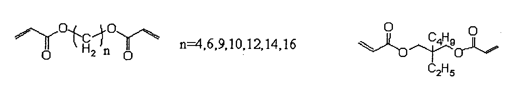


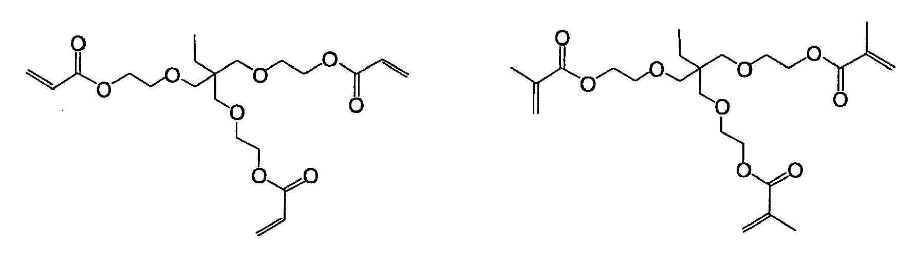

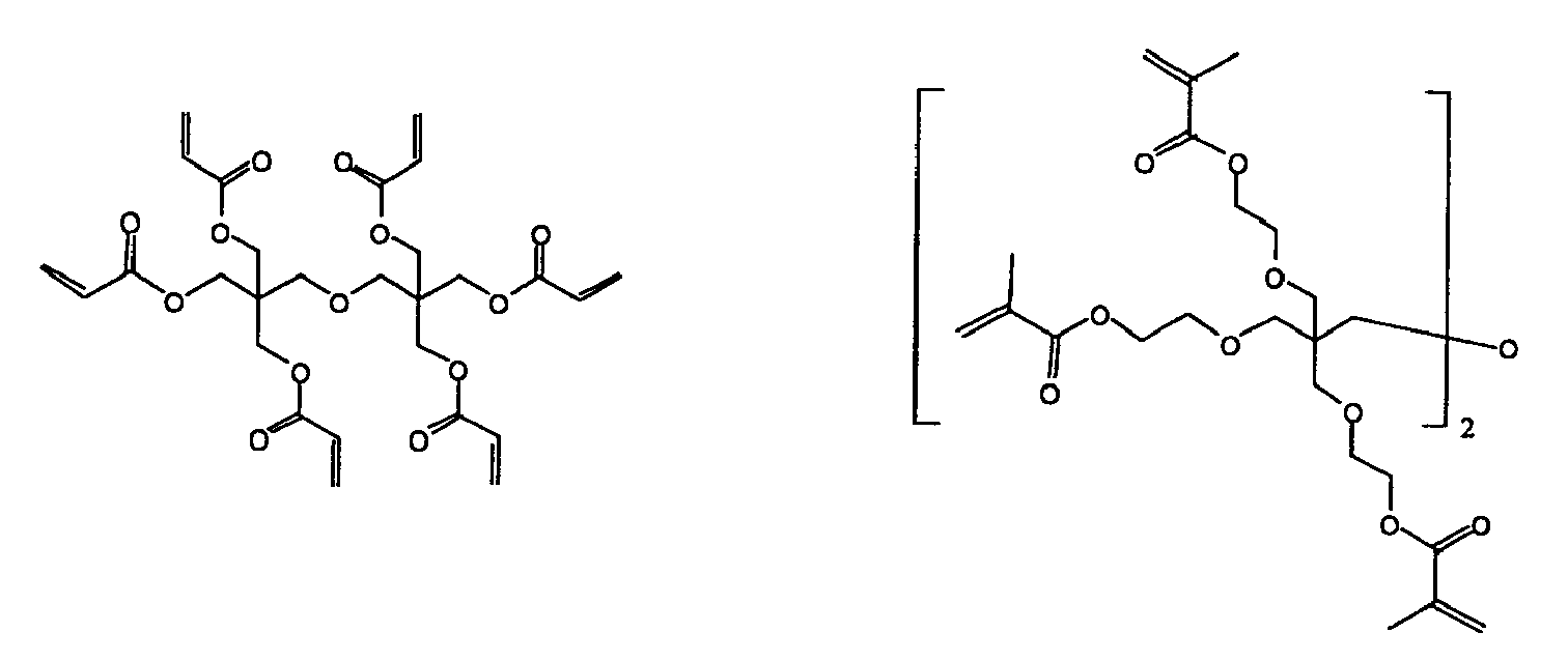
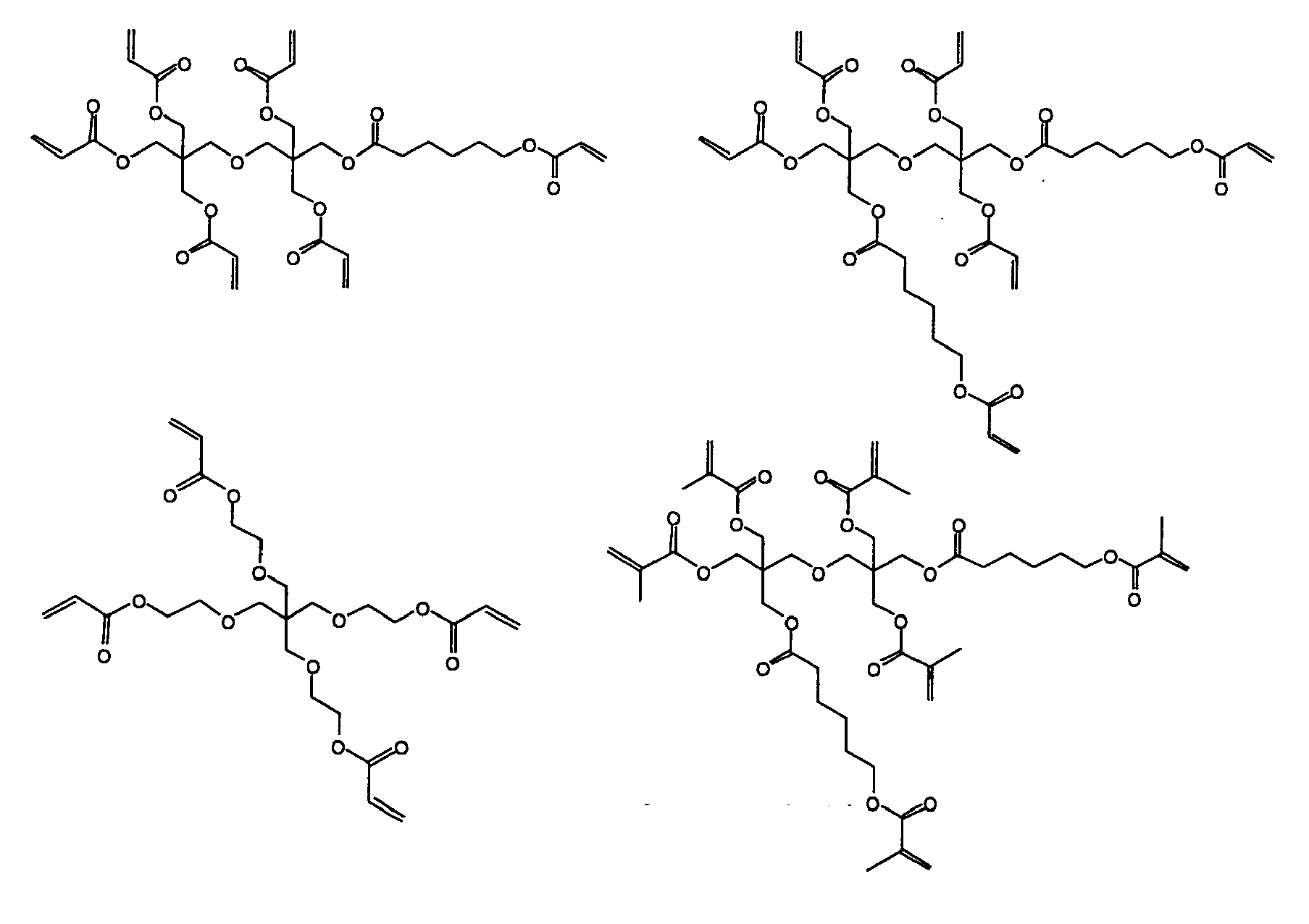


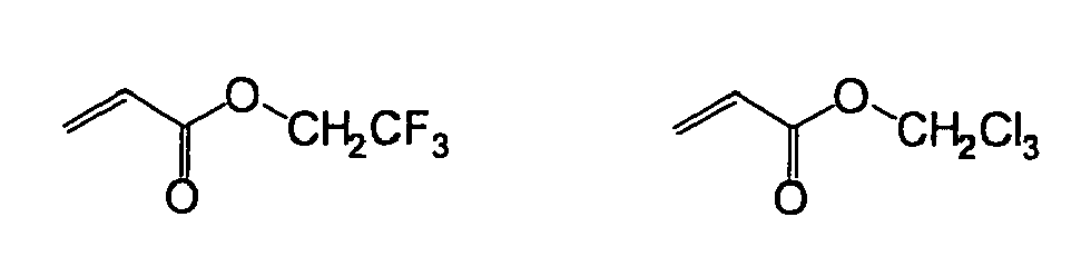


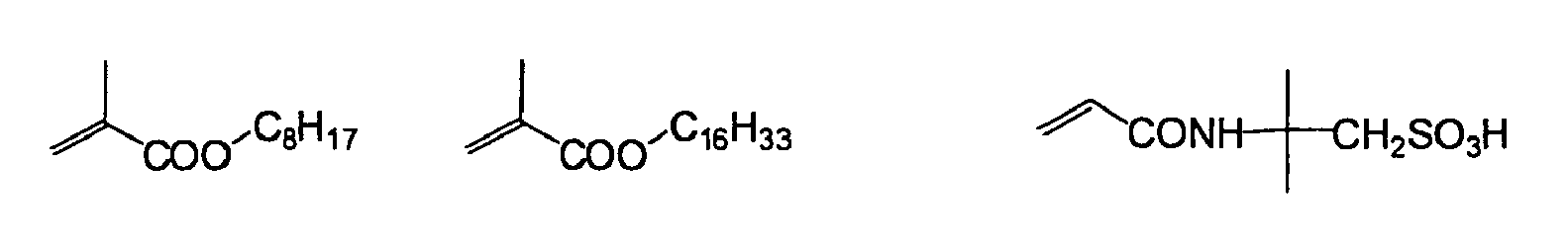


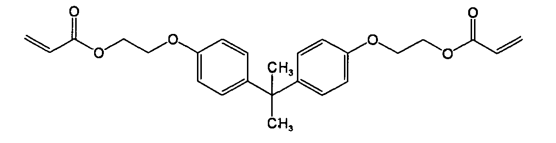
- The organic layer of the invention is generally obtained by coating and curing the polymerizing composition and, the polymerizing composition in the invention may contain a polymerization initiator. In the case where a photopolymerization initiator is used, its amount is preferably at least 0.1 mol% of the total amount of the polymerizing compound, more preferably from 0.5 to 2 mol%. By setting the thus-designed composition, polymerization reaction though an active ingredient forming reaction may be suitably controlled. Examples of the photopolymerization initiator include Ciba Speciality Chemicals' commercial products, Irgacure series (e.g., Irgacure 651, Irgacure 754, Irgacure 184, Irgacure 2959, Irgacure 907, Irgacure 369, Irgacure 379, Irgacure 819), Darocure series (e.g., Darocure TPO, Darocure 1173), Quantacure PDO; Sartomer's commercial products, Ezacure series (e.g., Ezacure TZM, Ezacure TZT), etc.
- The method for forming the organic layer is not specifically defined. For example, the layer may be formed according to a solution coating method or a vacuum film formation method. The solution coating method is, for example, a dipping method, an air knife coating method, a curtain coating method, a roller coating method, a wire bar coating method, a gravure coating method, a slide coating method, or an extrusion coating method using a hopper as in
USP 2681294 . The vacuum film formation method is not specifically defined, but is preferably a film formation method by vapor deposition or plasma CVD. In the invention, the polymer may be applied for coating as its solution, or a hybrid coating method along with an inorganic material, as inJP-A 2000-323273 2004-25732 - In the invention, the above-mentioned polymerizing compound is polymerized and crosslinked through irradiation with heat or various energy rays, thereby forming an organic layer comprising a polymer as the main ingredient thereof. Examples of energy rays include UV rays, visible rays, IR rays, electron rays, X rays, gamma rays, etc. In the case where the compound is polymerized by heat, then a thermal polymerization initiator may be used; where it is polymerized with UV rays, then a photopolymerization initiator may be used; and where it is polymerized with visible rays, then a photopolymerization initiator and a sensitizer may be used. Of the above, preferred is a method of polymerizing and crosslinking a polymerizing compound in the presence of a photopolymerization initiator.
- In the invention, in general, a polymerizing compound-containing composition is cured through irradiation with light, and the light for radiation is generally a UV ray from a high-pressure mercury lamp or low-pressure mercury lamp. The radiation energy is preferably at least 0.5 J/cm2, more preferably at least 2 J/cm2. (Meth)acrylate compounds may suffer from interference in polymerization owing to oxygen in air, and therefore, in their polymerization, the oxygen concentration or the oxygen partial pressure is preferably lowered. In the case where the oxygen concentration in polymerization is lowered according to a nitrogen purging method, the oxygen concentration is preferably at most 2 %, more preferably at most 0.5 %. In the case where the oxygen partial pressure in polymerization is lowered by a pressure reduction method, the whole pressure is preferably at most 1000 Pa, more preferably at most 100 Pa. Especially preferred is UV polymerization with at least 2 J/cm2 energy radiation under a condition of reduced pressure of at most 100 Pa.
- The organic layer is preferably smooth. Regarding the smoothness of the organic layer, the mean roughness (Ra) of 1 µm2 of the layer is preferably at most 1 nm, more preferably at most 0.5 nm. Preferably, the rate of polymerization of monomer is at least 85 %, more preferably at least 88 %, even more preferably at least 90 %, still more preferably at least 92 %. The rate of polymerization as referred to herein means the ratio of the reacted polymerizing group to all the polymerizing group (acryloyl group and methacryloyl group) in the monomer mixture. The rate of polymerization may be quantitatively determined according to IR absorptiometry.
- The thickness of the organic layer is not specifically defined. However, when the layer is too thin, then its thickness could hardly keep uniformity; but when too thick, the layer may be cracked by external force applied thereto and its barrier-property may lower. From these viewpoints, the thickness of the organic layer is preferably from 50 nm to 2000 nm, more preferably from 200 nm to 1500 nm.
- As so mentioned in the above, the organic layer is preferably smooth. Regarding the smoothness of the organic layer, the mean roughness (Ra) of 1 µm2 of the layer is preferably at most 1 nm, more preferably at most 0.5 nm. The surface of the organic layer is required not to have impurities and projections such as particles. Accordingly, it is desirable that the organic layer is formed in a clean room. The degree of cleanness is preferably at most class 10000, more preferably at most class 1000.
- Preferably, the hardness of the organic layer is higher. It is known that, when the hardness of the organic layer is high, then the inorganic layer may be formed smoothly and, as a result, the barrier level of the gas barrier film is thereby improved. The hardness of the organic layer may be expressed as a microhardness based on a nano-indentation method. The microhardness of the organic layer is preferably at least 150 N/mm, more preferably at least 180 N/mm, even more preferably at least 200 N/mm.
- Two or more organic layers are preferably laminated. In this case, each layer may have the same composition or may have different compositions. In this case, it is preferred that at least one layer is the above-mentioned organic layer, and the other organic layer may be the above-mentioned organic layer or an organic layer derived from other composition. The organic layer also may be included as a layer have a composition continuously changing in the direction of the layer thickness with no definite interface between an organic layer and an inorganic layer, as illustrated in
USP-A 2004-46497 . - In the gas barrier film of the invention, a plastic film is in general used as the substrate film. The plastic film to be used is not particularly limited with respect to the material quality and thickness, etc. so far as it is a film capable of keeping a laminate of an organic layer, an inorganic layer and the like and can be properly chosen depending upon the use purpose or the like. Specific examples of the plastic film include thermoplastic resins such as polyester resins, methacrylic acid-maleic acid copolymers, polystyrene resins, transparent fluorocarbon resins, polyimides, fluorinated polyimide resins, polyamide resins, polyamide-imide resins, polyetherimide resins, cellulose acylate resins, polyurethane resins, polyetheretherketone resins, polycarbonate resins, alicyclic polyolefin resins, polyarylate resins, polyethersulfone resins, polysulfone resins, cycloolefin copolymers, fluorene ring-modified polycarbonate resins, alicyclic modified polycarbonate resins, fluorene ring-modified polyester resins and acryloylated compounds. Of those, polyester resin such as polyethylene terephthalate (PET), polyethylene naphthalate(PEN) is preferable.
- In the case where the gas barrier film of the invention is used as a substrate of a device such as organic EL devices as described later, it is preferable that the plastic film is composed of a raw material with heat resistance. Specifically, it is preferable that the plastic film is composed of a transparent raw material with high heat resistance having a glass transition temperature (Tg) of 100 °C or higher and/or a linear heat expansion coefficient of not more than 40 ppm/°C. The Tg and linear heat expansion coefficient can be adjusted by an additive or the like. Examples of such a thermoplastic resin include polyethylene naphthalate (PEN: 120 °C), polycarbonate (PC: 140 °C), alicyclic polyolefins (for example, ZEONOR 1600, manufactured by Zeon Corporation: 160 °C), polyarylate (PAr: 210 °C), polyethersulfone (PES: 220 °C), polysulfone (PSF: 190 °C), cycloolefin copolymers (COC: a compound described in Example 1 of
JP-A-2001-150584 JP-A-2000-227603 JP-A-2000-227603 JP-A-2002-80616 - In the case where the gas barrier film of the invention is used in combination with a polarizing plate, it is preferable that the gas barrier layer surface of the gas barrier film (surface on which the laminate including at least one inorganic layer and at least one organic layer is formed) is faced at the inside of a cell and is disposed in the innermost (adjacent to the device). At that time, since the gas barrier film is disposed in the inside of the cell relative to the polarizing plate, a retardation value of the gas barrier film is important. As to a use form of the gas barrier film in such an embodiment, it is preferable that a barrier film using a base material film having a retardation value of not more than 10 nm and a circular polarizing plate ((quarter-wave plate) + (half-wave plate) + (linear polarizing plate)) are laminated and used, or that a linear polarizing plate is combined with a gas barrier film using a base material film having a retardation value of from 100 nm to 180 nm, which can be used as a quarter-wave plate, and used.
- Examples of the base material film having a retardation of not more than 10 nm include cellulose triacetate (FUJITAC, manufactured by Fujifilm Corporation), polycarbonates (PURE-ACE, manufactured by Teijin Chemicals Ltd.; and ELMECH, manufactured by Kaneka Corporation), cycloolefin polymers (ARTON, manufactured by JSR Corporation; and ZEONOR, manufactured by Zeon Corporation), cycloolefin copolymers (APEL (pellet), manufactured by Mitsui Chemicals, Inc.; and TOPAS (pellet), manufactured by Polyplastics Co., Ltd.), polyarylates (U100 (pellet), manufactured by Unitika Ltd.) and transparent polyimides (NEOPULIM, manufactured by Mitsubishi Gas Chemical Company).
- Also, films obtained by properly stretching the foregoing film to adjust it so as to have a desired retardation value can be used as the quarter-wave plate.
- In view of the matter that the gas barrier film of the invention is utilized as a device such as organic EL devices, the plastic film must be transparent, namely its light transmittance is usually 80% or more, preferably 85% or more, and more preferably 90% or more. The light transmittance can be measured by a method described in JIS-K7105, namely by measuring a total light transmittance and an amount of scattered light using an integrating sphere type light transmittance analyzer and subtracting the diffuse transmittance from the total light transmittance.
- Even in the case where the gas barrier film of the invention is used for display use, for example, when it is not disposed on the side of an observer, the transparency is not always required. Accordingly, in such case, an opaque material can also be used as the plastic film. Examples of the opaque material include known liquid crystal polymers such as polyimides and polyacrylonitrile.
- The thickness of the plastic film to be used for the gas barrier film of the invention is properly chosen depending upon the use and therefore, is not particularly limited. It is typically from 1 to 800 µm, and preferably from 10 to 200 µm. These plastic films may have a functional layer such as a transparent conductive layer and a primer layer. The functional layer is described in detail in paragraphs 0036 to 0038 of
JP-A-2006-289627 - The display devices of the invention include liquid crystal display devices, touch panels, organic EL devices, thin-film transistor (TFT) imaging display devices, and electronic papers.
- The reflection type liquid crystal display device is configured to include a lower substrate, a reflection electrode, a lower alignment film, a liquid crystal layer, an upper alignment film, a transparent electrode, an upper substrate, a λ/4 plate and a polarizing film in order from the lower side. In the case of giving a color displaying function to the reflection type liquid crystal display device, it is preferable to further provide a color filter layer between the reflection electrode and the lower alignment film or between the upper alignment film and the transparent electrode.
- Also, the transmission type liquid crystal display device is configured to include a backlight, a polarizing plate, a λ/4 plate, a lower transparent electrode, a lower alignment film, a liquid crystal layer, an upper alignment film, an upper transparent electrode, an upper substrate, a λ/4 plate and a polarizing plate in order from the lower side. Also, in the case of giving a color displaying function to the transmission type liquid crystal display device, it is preferable to further provide a color filter layer between the lower transparent electrode and the lower alignment film or between the upper alignment film and the upper transparent electrode.
- Though the structure of the liquid crystal layer is not particularly limited, it is preferably of, for example, a TN (twisted nematic) type, an STN (super twisted nematic) type, an HAN (hybrid aligned nematic) type, a VA (vertically alignment) type, an ECB (electrically controlled birefringence) type, an OCB (optically compensated bend) type, a CPA (continuous pinwheel alignment) type or an IPS (in-plane switching) type.
- As the touch panel, one obtained by applying the gas barrier film of the invention onto a substrate described in, for example,
JP-A-5-127822 JP-A-2002-48913 - An "organic EL device" means an organic electroluminescent device. The organic EL device has a cathode and an anode on a substrate and has an organic compound layer including an organic light-emitting layer between the both electrodes. In view of properties of the light-emitting device, it is preferable that at least one electrode of the anode and the cathode is transparent.
- In the invention, an embodiment of the laminate of the organic compound layer is preferably an embodiment in which a hole transport layer, a light-emitting layer and an electron transport layer are laminated in order from the anode side. Furthermore, a charge blocking layer may be provided between the hole transport layer and the light-emitting layer or between the light-emitting layer and the electron transport layer. A hole injection layer may be provided between the anode and the hole transport layer; and an electron injection layer may be provided between the cathode and the electron transport layer. The light-emitting layer may comprise only one layer, or may be divided into a first light-emitting layer, a second light-emitting layer, and a third light-emitting layer, and the like. Each of the layers may be divided into plural secondary layers.
- Hereinafter, each element constituting the organic EL device is described in detail.
- As the substrate for use in the organic EL device of the invention, usable is the gas barrier film of the invention or a substrate for use in known organic EL devices. When a gas barrier film is used as a substrate, usable are gas barrier films described in
JP-A-2004-136466 JP-A-2004-148566 JP-A-2005-246716 JP-A-2005-262529 - The thickness of the substrate for use in the invention is not specifically limited, and is preferably 30 µm to 700 µm, more preferably 40 µm to 200 µm, further more preferably 50 µm to 150 µm. In each case, the haze value of the substrate is preferably 3 % or less, more preferably 2 % or less, and further more preferably 1 % or less. The all transmission of the substrate is preferably 70 % or more, more preferably 80 % or more, and further more preferably 90 % or more.
- In general, the anode may have a function as an electrode capable of supplying a hole into the organic compound layer and is not particularly limited as to its shape, structure and size or the like. The anode can be properly chosen among known electrode materials depending upon the use and purpose of the light-emitting device. As described previously, the anode is usually provided as a transparent anode. The transparent anode is described in detail in New Developments of Transparent Conducting Films, supervised by SAWADA, Yutaka (published by CMC Publishing Co., Ltd., 1999). In the case of using a plastic base material with low heat resistance, a transparent anode obtained through fabrication at a low temperature of not higher than 150 °C using ITO or IZO is preferable.
- In general, the cathode may have a function as an electrode capable of injecting an electron into the organic compound layer and is not particularly limited as to its shape, structure and size or the like. The cathode can be properly chosen among known electrode materials depending upon the use and purpose of the light-emitting device.
- As materials constituting the cathode, for example, metals, alloys, metal oxides, electric conductive materials or mixtures thereof can be exemplified. Specific examples thereof include alkaline earth metals (for example, Mg and Ca) , gold, silver, lead, aluminum, a sodium-potassium alloy, a lithium-aluminum alloy, a magnesium-silver alloy, indium and rare earth metals (for example, ytterbium). Though these materials may be used singly, from the standpoint of making stability and electron injection properties compatible with each other, two or more kinds of these materials can be favorably used in combination.
- Of these, in view of electron injection properties, the material constituting the cathode is preferably an alkali metal or an alkaline earth metal; and in view of excellent storage stability, the material constituting the cathode is preferably a material composed mainly of aluminum.
- The material composed mainly of aluminum refers to aluminum alone or an alloy of aluminum and from 0.01 to 10% by mass of an alkali metal or an alkaline earth metal or a mixture thereof (for example, a lithium-aluminum alloy and a magnesium-aluminum alloy). The cathode material is described in detail in
JP-A-2-15595 JP-A-5-121172 - The thickness of the cathode can be properly chosen depending upon the material constituting the cathode and cannot be unequivocally defined. However, the thickness of the cathode is in general from about 10 nm to 5 µm, and preferably from 50 nm to 1 µm.
- Also, the cathode may be transparent or opaque. The transparent cathode can be formed by thinly fabricating the cathode material in a thickness of from 1 to 10 nm and further laminating a transparent conductive material such as ITO and IZO thereon.
- The organic electroluminescent device of the invention has at least one organic compound layer including a light-emitting layer. As described previously, examples of other organic compound layers than the organic light-emitting layer include respective layers such as a hole transport layer, an electron transport layer, a charge blocking layer, a hole injection layer and an electron injection layer.
- The organic light-emitting layer is a layer having a function such that at the time of application of an electric field, it receives a hole from the anode, the hole injection layer or the hole transport layer and receives an electron from the cathode, the electron injection layer or the electron transport layer to provide a field of recombination of the hole and the electron, thereby achieving light emission. The light-emitting layer may be constituted of only a light-emitting material or may be configured as a mixed layer of a host material and a light-emitting material. The light-emitting material may be a fluorescent light-emitting material or a phosphorescent light-emitting material; and a dopant may be a single material or a combination of two or more kinds of materials. The host material is preferably a charge transport material. The host material may be a single material or a combination of two or more kinds of materials, and examples thereof include a constitution of a mixture of an electron transporting host material and a hole transporting host material. Furthermore, the light-emitting layer may contain a material which does not have charge transporting properties and does not emit light. Also, the light-emitting layer may be a single layer or may be configured of two or more layers, and the respective layers may emit light in a different luminescent color.
- Examples of the fluorescent light-emitting material which can be used in the invention include compounds, for example, benzoxazole derivatives, benzimidazole derivatives, benzothiazole derivatives, styrylbenzene derivatives, polyphenyl derivatives, diphenylbutadiene derivatives, tetraphenylbutadiene derivatives, naphthalimide derivatives, coumarin derivatives, condensed aromatic compounds, perynone derivatives, oxadiazole derivatives, oxazine derivatives, aldazine derivatives, pyralidine derivatives, cyclopentadiene derivatives, bisstyrylanthracene derivatives, quinacridone derivatives, pyrrolopyridine derivatives, thiadiazolopyridine derivatives, cyclopentadiene derivatives, styrylamine derivatives, diketopyrrolopyrrole derivatives, aromatic dimethylidyne derivatives, various metal complexes represented by metal complexes of 8-quinolinol derivatives and pyrromethene derivatives, polymer compounds (for example, polythiophene, polyphenylene and polyphenylenevinylene) and organosilane derivatives.
- Examples of the phosphorescent light-emitting material include complexes containing a transition metal atom or a lanthanoid atom.
- The transition metal atom is not particularly limited, and preferred examples thereof include ruthenium, rhodium, palladium, tungsten, rhenium, osmium, iridium and platinum, with rhenium, iridium and platinum being more preferable.
- Examples of the lanthanoid atom include lanthanum, cerium, praseodymium, neodymium, samarium, europium, gadolinium, terbium, dysprosium, holmium, erbium, thulium, ytterbium and lutetium. Of these lanthanoid atoms, neodymium, europium and gadolinium are preferable.
- Examples of a ligand of the complex include ligands described in G. Wilkinson, et al., Comprehensive Coordination Chemistry, published by Pergamon Press, 1987; H. Yersin, Photochemistry and Photophysics of Coordination Compounds, published by Springer-Verlag, 1987; and YAMAMOTO, Akio, Organometallic Chemistry - Principles and Applications, published by Shokabo Publishing Co., Ltd., 1982.
- Also, examples of the host material which is contained in the light-emitting layer in the invention include materials as enumerated in the following paragraphs of hole injection layer, hole transport layer, electron injection layer and electron transport layer as well as a material having a carbazole skeleton, a material having a diarylamine skeleton, a material having a pyridine skeleton, a material having a pyrazine skeleton, a material having a triazine skeleton and a material having an arylsilane skeleton.
- The hole injection layer and the hole transport layer are each a layer having a function to receive a hole from the anode or the anode side to transport it into the cathode side. Specifically, the hole injection layer and the hole transport layer are each preferably a layer containing a carbazole derivative, a triazole derivative, an oxazole derivative, an oxadiazole derivative, an imidazole derivative, a polyarylalkane derivative, a pyrazoline derivative, a pyrazolone derivative, a phenylenediamine derivative, an arylamine derivative, an amino-substituted chalcone derivative, a styrylanthracene derivative, a fluorenone derivative, a hydrazone derivative, a stilbene derivative, a silazane derivative, an aromatic tertiary amine compound, a styrylamine compound, an aromatic dimethylidene based compound, a porphyrin based compound, an organosilane derivative, carbon or the like.
- The electron injection layer and the electron transport layer are each a layer having a function to receive an electron from the cathode or the cathode side to transport it into the anode side. Specifically, the electron injection layer and the electron transport layer are each preferably a layer containing a triazole derivative, an oxazole derivative, an oxadiazole derivative, an imidazole derivative, a fluorenone derivative, an anthraquinodimethane derivative, an anthrone derivative, a diphenylquinone derivative, a thiopyran dioxide derivative, a carbodiimide derivative, a fluorenylidenemethane derivative, a distyrylpyrazine derivative, aromatic ring tetracarboxylic acid anhydrides of naphthalene, perylene, etc., a phthalocyanine derivative, a metal complex of every kind represented by metal complexes of 8-quinolinol derivatives and metal complexes composed of, as a ligand, metal phthalocyanine, benzoxazole or benzothiazole, an organosilane derivative or the like.
- The hole blocking layer is a layer having a function to prevent a phenomenon in which the hole which has been transported into the light-emitting layer from the anode side passes through into the cathode side from occurring. In the invention, the hole blocking layer can be provided as an organic compound layer which is positioned adjacent to the light-emitting layer on the cathode side.
- Examples of an organic compound constituting the hole blocking layer include aluminum complexes such as BAlq, triazole derivatives and phenanthroline derivatives such as BCP. Also, a layer having a function to prevent a phenomenon in which the electron which has been transported into the light-emitting layer from the cathode side passes through into the anode side from occurring may be provided on the position adjacent to the light-emitting layer on the anode side. The hole injection layer and hole transport layer may serve this function.
- The gas barrier film of the invention can be used also as a sealing film for solar cell devices. Preferably, the gas barrier film of the invention is used for sealing a solar cell device in such a manner that its adhesive layer is on the side near to the solar cell device. The solar cell devices for which the gas barrier film of the invention is favorably used are not specifically defined. For example, they include single crystal silicon-based solar cell devices, polycrystalline silicon-based solar cell devices, single-junction or tandem-structure amorphous silicon-based solar cell devices, gallium-arsenic (GaAs), indium-phosphorus (InP) or the like III-V Group compound semiconductor-based solar cell devices, cadmium-tellurium (CdTe) or the like II-VI Group compound semiconductor-based solar cell devices,
copper/indium/selenium (CIS-based),
copper/indium/gallium/selenium (CIGS-based),
copper/indium/gallium/selenium/sulfur (CIGSS-based) or the like I-III-VI Group compound semiconductor-based solar cell devices, dye-sensitized solar cell devices, organic solar cell devices, etc. Above all, in the invention, the solar cell devices are preferably copper/indium/selenium (CIS-based),
copper/indium/gallium/selenium (CIGS-based),
copper/indium/gallium/selenium/sulfur (CIGSS-based) or the like I-III-VI Group compound semiconductor-based solar cell devices. - The characteristic features of the invention are hereunder described in more detail with reference to the following Examples. Materials, use amounts, proportions, treatment contents, treatment procedures and the like shown in the following Examples can be properly changed. Accordingly, the scope of the invention should not be limitedly construed by the following specific examples.
- Gas barrier films having an inorganic layer and an organic layer provided on a substrate film (samples Nos. 101 to 115) were produced according to the process mentioned below. The details of the constitution of each gas barrier film are shown in Table 1. The substrate film is a polyethylene naphthalate film (PEN, Teijin-Dupont's Q65A having a thickness of 100 µm).
- Using a reactive sputtering apparatus, an inorganic layer of aluminium oxide was formed. The concrete film formation condition is shown below.
- The pressure in the vacuum chamber of the reactive sputtering apparatus was reduced to an ultimate pressure of 5 × 10⁻⁴ Pa, using an oil rotatory pump and a turbomolecular pump. Next, argon was introduced into it as a plasma gas; and a power of 2000 W was applied to it from a plasma source. A high-purity oxygen gas was introduced into the chamber, and the film formation pressure was controlled at 0.3 Pa for a predetermined period of time to form an inorganic layer of aluminium oxide. Thus formed, the aluminium oxide film had a thickness of 40 nm and a film density of 3.01 g/cm3.
- The organic layer was formed according to five methods of a solution-coating film formation method under normal pressure (organic layers Y, W, V, U) and a flash vapor deposition method under reduced pressure (organic layer Z). The details of film formation are shown below.
- 9 g of a photopolymerizing acrylate, tripropylene glycol diacrylate (TPGDA, by Daicel Sytec) and 0.1 g of a photopolymerization initiator (Ciba Specialty Chemicals' Irgacure 907) were dissolved in 190 g of methyl ethyl ketone to prepare a coating solution. The coating solution was applied onto a substrate film, with a wire bar, and then irradiated with UV rays at an illuminance of 350 mW/cm2 and at a radiation dose of 500 mJ/cm2, using an air-cooling metal halide lamp of 160 W/cm (by Eyegraphics) with nitrogen purging to an oxygen concentration of at most 0.1 %, thereby forming an organic layer (Y). The film thickness was about 500 nm.
- An organic layer (W) was formed in the same manner as that for the organic layer (Y), for which, however, dipentaerythritol hexaacrylate (DPHA, by Shin-Nakamura Chemical Industry) was used as the photopolymerizing acrylate in place of tripropylene glycol diacrylate (TPGDA). The film thickness was about 500 nm.
- 9.7 g of a photopolymerizing acrylate, butylethylpropanediol diacrylate (BEPGA, by Kyoei Chemical) and 0.3 g of a photopolymerization initiator (Lambertispa's Ezacure-TZT) were mixed to prepare a vapor deposition liquid. The vapor deposition liquid was applied onto a substrate for vapor deposition thereon, according to a flash vapor deposition method under a condition of inner pressure of 3 Pa in the vacuum chamber. Next, under the same vacuum degree condition, this was irradiated with UV rays at a radiation dose of 2 J/cm2, thereby forming an organic layer (Z). The film thickness was about 1200 nm. For forming an organic layer Z, used was an organic/inorganic laminate film formation device, Guardian 200 (by Vitex Systems).
- 9 g of a photopolymerizing acrylate, bisphenol A-type epoxyacrylate (Shin-Nakamura Chemical's NK OligoEA-1020) and 0.1 g of a photopolymerization initiator (Ciba Specialty Chemicals' Irgacure 907) were dissolved in 190 g of methyl ethyl ketone to prepare a coating solution. The coating solution was applied onto a substrate film, using a wire bar, and then irradiated with UV rays at an illuminance of 350 mW/cm2 and at a radiation dose of 500 mJ/cm2, using an air-cooling metal halide lamp of 160 W/cm (by Eyegraphics) with nitrogen purging to an oxygen concentration of at most 0.1 %, thereby forming an organic layer (V). The film thickness was about 500 nm.
- An organic layer (U) was formed in the same manner as that for the organic layer (V), for which, however, epoxyacrylate (Daicel Sytec's EB3702) was used as the photopolymerizing acrylate in place of bisphenol A-type epoxyacrylate (Shin-Nakamura Chemical's NK OligoEA-1020). The film thickness was about 500 nm.
- The barrier resin layer was formed according to the following six methods. The details of film formation are shown below.
- Polyvinyl alcohol (PVA 117H by Kuraray) was dissolved in pure water at 2 % by weight to prepare a coating solution. The coating solution was applied onto a substrate film, using a wire bar, and dried at 80°C to form a barrier resin layer (P-1) thereon. The film thickness was about 700 nm.
- Vinylidene chloride copolymer (Saran Resin F216, by Asahi Kasei) was dissolved in a mixed solvent of toluene/tetrahydrofuran = 1/2 (by weight) at 15 % by weight to prepare a coating solution. The coating solution was applied onto a substrate film, using a wire bar, and dried at 105°C to form a barrier resin layer (P-2) thereon. The film thickness was about 2.5 µm.
- Ethylene-vinyl alcohol copolymer (Soanol 30L, by Nippon Synthetic Chemical Industry) was dissolved in a mixed solvent of pure water/isopropanol = 1/1 (by weight) at 12 % by weight to prepare a coating solution. The coating solution was applied onto a substrate film, using a wire bar, and dried at 110°C to form a barrier resin layer (P-3) thereon. The film thickness was about 2 µm.
- A dispersion (1) prepared by dispersing synthetic mica (tetrasilylic mica (Na-Ts), by Topy Industry) in pure water at 0.65 % by weight, and a solution (2) prepared by dissolving polyvinyl alcohol (PVA 210, by Kuraray) in pure water at 0.325 % by weight were mixed in a ratio (by volume), in terms of the solid content, of dispersion (1) to solution (2), (1) / (2) = 3/7, to thereby prepare a coating liquid. The coating liquid was applied onto a substrate film, using a wire bar, to form a barrier resin layer (P-4) thereon. The film thickness was about 1 µm. [3-5] Formation of barrier resin layer (P-5):
- A barrier resin layer (P-5) was formed in the same manner as that for the barrier resin layer (P-4), for which, however, hydroxyethyl cellulose (by Wako Pure Chemicals) was used in place of polyvinyl alcohol in the solution (2). The film thickness was about 1 µm.
- 9 g of a photopolymerizing acrylate, dipentaerythritol hexaacrylate (DPHA, by Shin-Nakamura Chemical) and 0.1 g of a photopolymerization initiator (Ciba Specialty Chemicals' Irgacure 907) were dissolved in 190 g of methyl ethyl ketone to prepare a coating solution. The coating solution was applied onto a substrate film, using a wire bar, and then irradiated with UV rays at an illuminance of 350 mW/cm2 and at a radiation dose of 1 J/cm2, using an air-cooling metal halide lamp of 160 W/cm (by Eyegraphics) with nitrogen purging to an oxygen concentration of at most 0.1 %, thereby forming a barrier resin layer (P-6). The film thickness was about 1 µm.
- Gas barrier films were produced by forming, on a substrate film, the above-mentioned inorganic layer and organic layer in order according to the constitution of the samples shown in Table 1. The films were produced according to the following three methods.
- An organic layer and an inorganic layer were alternately laminated on a substrate film. An inorganic layer was laminated on an organic layer as follows: An organic layer was first formed by solution coating, and then this was put into a vacuum chamber, in which the pressure was reduced to a vacuum degree of at most 10-3 Pa. This was kept in the chamber for a predetermined period of time, and then an inorganic layer was formed on it. An organic layer was laminated on the inorganic layer as follows: Immediately after the formation of the inorganic layer, an organic layer was formed thereon according to a solution coating method.
- Using the above-mentioned organic/inorganic laminate film formation apparatus, Guardian 200, an organic layer and an inorganic layer were laminated. In this apparatus, both the organic layer and the inorganic layer are formed in a reduced pressure environment, and the film formation chambers for organic layer and inorganic layer are connected to each other. In this, therefore, the two layers could be continuously formed in a reduced pressure environment. Accordingly, the film is not exposed to air until the completion of barrier film formation.
- A first organic layer was formed on a substrate according to a solution coating method. Next, the substrate having the first organic layer was put into a vacuum chamber, in which the pressure was reduced to a vacuum degree of at most 10-3 Pa. This was kept in the chamber for a predetermined period of time, and then an inorganic layer and an organic layer were formed alternately.
- Using the apparatus mentioned below, physical properties of gas barrier films were evaluated.
- An ultra-thin piece of a film sample was observed with a scanning electromicroscope, Hitachi's "S-900 Model".
- MOCON's "PERMATRAN-W3/31" (condition: 40°C, 90 % RH) was used. The data lower than the detection limit of the MOCON's apparatus, 0.01 g/m2/day were supplemented according to the following method. First, the surface of the gas barrier film is directly coated with a metal Ca by vapor deposition, then the film and a glass substrate were sealed up with a commercially-available organic EL sealant in such a manner that the Ca-coated surface of the film could face inside, thereby preparing a test sample. Next, the test sample is kept under the above-mentioned temperature/humidity condition, and the metal Ca coating on the gas barrier film was checked for the optical density change thereof (the metal gloss reduces owing to hydroxylation or oxidation), from which the water vapor permeability through the film is determined. For the details, referred to is the method described in the following Reference.
- G. NISATO, P. C. P. BOUTEN, P. J. SLIKKERVEER, et al.; SID Conference Record of the International Display Research Conference pp.1435-1438.
- An inorganic layer was formed on an Si wafer to prepare a test sample, and this was analyzed with Rigaku Denki's ATX-G. From the found data, the film density of the thin film of inorganic layer was computed.
[Table 1] Sample No. Layer Constitution Lamination Method Barrier Resin Layer Water Vapor Permeability (g/m2day) 101 PEN/Y/X/Y/X lamination A - 0.01 102 P-1/PEN/Y/X/Y/X lamination A P-1 0.01 103 P-2/PEN/Y/X/Y/X lamination A P-2 0.01 104 P-3/PEN/Y/XlY/X lamination A P-3 0.01 105 PEN/Z/X/Z/X lamination B - 0.005 106 P-1/PEN/Z/X/Z/X lamination B P-1 0.005 107 P-2/PEN/Z/X/Z/X lamination B P-2 0.005 108 P-3/PEN/Z/X/Z/X lamination B P-3 0.005 109 P-4/PEN/Z/X/Z/X lamination B P-4 0.005 110 P-5/PEN/Z/X/Z/X lamination B P-5 0.005 111 PEN/Y/X/Z/X lamination C - 0.007 112 P-4/PEN/Y/X/Z/X lamination C P-4 0.007 113 P-5/PEN/Y/X/Z/X lamination C P-5 0.007 114 PEN/W/X/W/X lamination A - 0.008 115 P-6/PEN/W/X/W/X lamination A P-6 0.008 116 P-1/PEN/V/X/V/X lamination A P-1 0.007 117 P-1/PEN/U/X/U/X lamination A P-1 0.007 - Gas barrier films (samples Nos. 201 to 208)as in Table 2 were produced in the same manner as in Example 1, for which, however, polyethylene terephthalate (PET, thickness 100 µm, Toray's Lumirror T60) was used as a substrate film.
[Table 2] Sample No. Layer Constitution Lamination Method Barrier Resin Layer Water Vapor Permeability (g/m2day) 201 PET/Y/X/Y/X lamination A - 0.011 202 P-1/PET/Y/X/Y/X lamination A P-1 0.011 203 P-2/PET/Y/X/Y/X lamination A P-2 0.011 204 P-3/PET/Y/X/Y/X lamination A P-3 0.011 205 PET/Z/X/Z/X lamination B - 0.006 206 P-1/PET/Z/X/Z/X lamination B P-1 0.006 207 P-2/PET/Z/X/Z/X lamination B P-2 0.006 208 P-3/PET/Z/X/Z/X lamination B P-3 0.006 209 P-1/PET/V/X/V/X lamination A P-1 0.008 210 P-1/PET/U/X/U/X lamination A P-1 0.008 - An ITO film-having conductive glass substrate (surface resistivity, 10 Ω/square) was washed with 2-propanol, and then processed for UV ozone treatment for 10 minutes. On the substrate (anode), the following organic compound layers were formed in order by vapor deposition according to a vacuum vapor deposition method.
- Copper phthalocyanine: film thickness 10 nm.
- N,N'-diphenyl-N,N'-dinaphthylbenzidine: film thickness 40 nm.
- Tris(8-hydroxyquinolinato)aluminium: film thickness 60 nm.
- Finally, 1 nm of lithium fluoride and 100 nm of metal aluminium were formed in order by vapor deposition, thereby forming a cathode; and a silicon nitride film having a thickness of 3 µm was formed on it according to a parallel plate CVD method, thereby constructing an organic EL device.
- Using a thermosetting adhesive (Epotec 310, by Daizo-Nichimori), the barrier film produced in Example 1 and the organic EL device substrate were stuck together in such a manner that the barrier layer of the film could be on the side of the organic EL device, and heated at 65°C for 3 hours to cure the adhesive. 20 test pieces of every sample of the thus-sealed organic EL device (samples Nos. 301 to 315) were prepared.
- Just after produced, the organic EL device (samples Nos. 301 to 315) was tested for light emission under application of 7 V thereto, using a source measure unit (SMU2400 Model by Keithley). Using a microscope, the light-emitting surface was observed, which confirmed uniform light emission by every device with no dark spot.
- Next, the devices were stored in a dark room at 60°C and 90 % RH for 24 hours, and then tested for light emission. The proportion of the test pieces that gave dark spots larger than 300 µm in diameter is defined as a failure rate. Table 3 shows the failure rate of every tested device.
- Using the gas barrier film produced in Example 2 as a sealing film, sealed organic EL device (samples Nos. 401 to 408) were produced. In applying the gas-barrier layer to the organic EL device, used was a UV-curable adhesive (XNR5516HV, by Nagase-Ciba) but not a thermosetting adhesive. The adhesive was cured with UV rays in an argon gas-purged globe box to adhere the film and the device. Like in Example 3, the samples were stored at 60°C and 90 % RH for 24 hours and tested, and the failure rate was computed. The results are shown in Table 4.
- The gas barrier film produced in Example 1 was introduced into a vacuum chamber, in which a transparent electrode of a thin ITO film having a thickness of 0.2 µm was formed on the film by DC magnetron sputtering with an ITO target. The ITO film-having gas barrier film was put into a washing chamber, and washed with 2-propanol therein, and then processed for UV-ozone treatment for 30 minutes. Using the substrate, an organic EL device (samples Nos. 501 to 508) was produced in the same manner as in Example 3. In the device, both the substrate and the sealing film comprise a resin as the main ingredient thereof, and therefore, the device was flexible as a whole. Like in Example 3, the devices were left at 60°C and 90 % RH for 24 hours, and then tested for the failure rate. The results are shown in Table 5.
[Table 3] Sample No. Gas barrier film Sample No. Failure Rate of Organic EL Device (%) Remarks 301 101 20 Comparative Sample 302 102 11 the Invention 303 103 5 the Invention 304 104 9 the Invention 305 105 11 Comparative Sample 306 106 4 the Invention 307 107 1 the Invention 308 108 3 the Invention 309 109 6 the Invention 310 110 9 the Invention 311 111 16 Comparative Sample 312 112 11 the Invention 313 113 14 the Invention 314 114 18 Comparative Sample 315 115 17 the Invention 316 116 8 the Invention 317 117 8 the Invention [Table 4] Sample No. Gas barrier film Sample No. Failure Rate of Organic EL Device (%) Remarks 401 201 22 Comparative Sample 402 202 14 the Invention 403 203 8 the Invention 404 204 13 the Invention 405 205 12 Comparative Sample 406 206 6 the Invention 407 207 3 the Invention 408 208 5 the Invention 409 209 10 the Invention 410 210 10 the Invention [Table 5] Sample No. Gas barrier film Sample No. Failure Rate of Organic EL Device (%) Remarks 501 101 30 Comparative Sample 502 102 16 the Invention 503 103 9 the Invention 504 105 17 Comparative Sample 505 106 7 the Invention 506 107 3 the Invention 507 109 10 the Invention 508 110 11 the Invention 509 116 14 the Invention 510 117 14 the Invention - From the results in Tables 3 to 5, it is confirmed that the barrier film having a barrier resin layer of the invention is superior to the barrier film not having a barrier resin layer in that the failure rate of the organic EL devices with the former is lower. It is also known that the barrier film of the invention is effective both for a sealing film and for a substrate of organic EL devices.
Claims (15)
- A gas barrier film having, on one surface of a substrate film, a gas-barrier layer comprising at least one organic region and at least one inorganic region, and having, as a barrier property-having layer, only a layer comprising a barrier property-having resin as the main ingredient of the layer on the other surface of the substrate film.
- The gas barrier film of Claim 1, wherein the gas-barrier layer comprises at least one organic layer and at least one inorganic layer.
- The gas barrier film of Claim 1 or 2, wherein the resin of the layer comprising a barrier property-having resin as the main ingredient of the layer is a polyvinyl alcohol.
- The gas barrier film of Claims 1 or 2, wherein the resin of the layer comprising a barrier property-having resin as the main ingredient of the layer is a polyfunctional acrylate.
- The gas barrier film of any one of Claims 2 to 4, wherein the organic layer is formed by curing a composition comprising at least one (meth)acrylate having a bisphenol skeleton.
- The gas barrier film of any one of Claims 2 to 5, wherein the main ingredient of the layer comprising a barrier property-having resin as the main ingredient of the layer is the same as the main ingredient of the organic layer.
- The gas barrier film of any one of Claims 2, and Claims 4 to 6, wherein both of the main ingredient of the organic layer and the layer comprising a barrier property-having resin as the main ingredient of the layer are derived from (meth) acrylate.
- The gas barrier film of any one of Claims 1 to 7, wherein the thickness of the layer comprising a barrier property-having resin as the main ingredient of the layer is from 0.5 to 30 µm.
- The gas barrier film of any one of Claims 1 to 8, which has a thickness of from 10 to 300 µm.
- The gas barrier film of any one of Claims 1 to 9, which is for display devices.
- A method for producing the gas barrier film of any one of Claims 1 to 10, which comprises providing the gas-barrier layer on a surface of a substrate film and then providing, on the other surface of the substrate film, the layer comprising a barrier property-having resin as the main ingredient of the layer.
- A display device comprising the gas barrier film of any one of Claims 1 to 10.
- The display device of Claim 12, wherein the gas barrier film is used for a substrate of the display device.
- The display device of Claim 12, wherein the gas barrier film is used for a sealing film of the display device.
- The display device of any one of Claims 12 to 14, wherein the gas barrier film is provided in such a manner that the layer comprising a barrier property-having resin as the main ingredient of the layer is on the outer side of the device.
Applications Claiming Priority (2)
| Application Number | Priority Date | Filing Date | Title |
|---|---|---|---|
| JP2007238857 | 2007-09-14 | ||
| JP2008140980A JP2009083465A (en) | 2007-09-14 | 2008-05-29 | Gas-barrier film and display element using this gas-barrier film |
Publications (3)
| Publication Number | Publication Date |
|---|---|
| EP2036717A2 true EP2036717A2 (en) | 2009-03-18 |
| EP2036717A3 EP2036717A3 (en) | 2009-11-11 |
| EP2036717B1 EP2036717B1 (en) | 2014-09-03 |
Family
ID=40193756
Family Applications (1)
| Application Number | Title | Priority Date | Filing Date |
|---|---|---|---|
| EP20080016209 Not-in-force EP2036717B1 (en) | 2007-09-14 | 2008-09-15 | Gas barrier film, and display device comprising the same |
Country Status (2)
| Country | Link |
|---|---|
| US (1) | US8067085B2 (en) |
| EP (1) | EP2036717B1 (en) |
Families Citing this family (7)
| Publication number | Priority date | Publication date | Assignee | Title |
|---|---|---|---|---|
| KR102059326B1 (en) * | 2012-03-29 | 2019-12-26 | 린텍 가부시키가이샤 | Gas barrier laminate, method for producing same, member for electronic devices, and electronic device |
| WO2014110780A1 (en) * | 2013-01-18 | 2014-07-24 | Liu Tajo | Isolation layer structure |
| WO2014110779A1 (en) * | 2013-01-18 | 2014-07-24 | Liu Tajo | Insulation layer structure |
| RU2672962C2 (en) | 2013-08-30 | 2018-11-21 | Июкф-Хю (Индастри-Юниверсити-Кооперейшн Фаундейшн Ханян Юниверсити) | Substrate structure and method for manufacture thereof |
| TWI653143B (en) * | 2014-07-24 | 2019-03-11 | 日商凸版印刷股份有限公司 | Laminated film and laminated body, and wavelength conversion sheet, backlight unit and electroluminescence light emitting unit |
| WO2017152103A1 (en) * | 2016-03-04 | 2017-09-08 | University Of Massachusetts | Vinyl hydroxyl ether resins |
| JP6469606B2 (en) * | 2016-03-17 | 2019-02-13 | 富士フイルム株式会社 | Gas barrier film |
Citations (22)
| Publication number | Priority date | Publication date | Assignee | Title |
|---|---|---|---|---|
| US2681294A (en) | 1951-08-23 | 1954-06-15 | Eastman Kodak Co | Method of coating strip material |
| JPH0215595A (en) | 1987-02-11 | 1990-01-19 | Eastman Kodak Co | Electroluminescent device with improved cathode |
| JPH05121172A (en) | 1991-01-29 | 1993-05-18 | Pioneer Electron Corp | Organic electroluminescence element |
| JPH05127822A (en) | 1991-10-30 | 1993-05-25 | Daicel Chem Ind Ltd | Touch panel |
| JPH09254303A (en) | 1996-03-22 | 1997-09-30 | Teijin Ltd | Transparent electrically conductive film |
| JP2000227603A (en) | 1998-11-30 | 2000-08-15 | Teijin Ltd | Liquid crystal display device and transparent conductive substrate suitable for the same |
| JP2000323273A (en) | 1999-05-07 | 2000-11-24 | Dainippon Printing Co Ltd | Electroluminescent element |
| JP2001150584A (en) | 1999-11-29 | 2001-06-05 | Nippon Zeon Co Ltd | Conductive substrate, and display element using the same |
| JP2002048913A (en) | 2000-08-04 | 2002-02-15 | Fuji Photo Film Co Ltd | Retardation film, circularly polarizing plate and reflective liquid crystal display device |
| JP2002080616A (en) | 2000-06-30 | 2002-03-19 | Sumitomo Bakelite Co Ltd | Polymer film for display element and substrate for display element using the same |
| JP2002322561A (en) | 2001-04-25 | 2002-11-08 | Sumitomo Bakelite Co Ltd | Sputtering film deposition method |
| JP2002361774A (en) | 2001-06-08 | 2002-12-18 | Dainippon Printing Co Ltd | Gas barrier film |
| JP3400324B2 (en) | 1997-11-17 | 2003-04-28 | 住友ベークライト株式会社 | Conductive film |
| JP2004025732A (en) | 2002-06-27 | 2004-01-29 | Fuji Photo Film Co Ltd | Gas barrier film |
| US20040046497A1 (en) | 2002-09-11 | 2004-03-11 | General Electric Company | Diffusion barrier coatings having graded compositions and devices incorporating the same |
| JP2004136466A (en) | 2002-10-15 | 2004-05-13 | Fuji Photo Film Co Ltd | Laminated gas barrier film, substrate comprising the same, and image display element using the film |
| JP2004148566A (en) | 2002-10-29 | 2004-05-27 | Fuji Photo Film Co Ltd | Gas barrier film, substrate composed of gas barrier film and image display element having gas barrier film |
| JP2005246716A (en) | 2004-03-03 | 2005-09-15 | Fuji Photo Film Co Ltd | Gas barrier laminated film and image display element using it |
| JP2005262529A (en) | 2004-03-17 | 2005-09-29 | Fuji Photo Film Co Ltd | Gas barrier film and organic electroluminescence element using it |
| JP2006035737A (en) | 2004-07-29 | 2006-02-09 | Teijin Ltd | Gas barrier polymer laminated film suitable for display |
| JP2006289627A (en) | 2005-04-06 | 2006-10-26 | Fuji Photo Film Co Ltd | Gas barrier film and organic device using the same |
| JP2007030451A (en) | 2005-07-29 | 2007-02-08 | Toppan Printing Co Ltd | Polyamide laminate |
Family Cites Families (5)
| Publication number | Priority date | Publication date | Assignee | Title |
|---|---|---|---|---|
| WO2002091064A2 (en) * | 2001-05-04 | 2002-11-14 | General Atomics | O2 and h2o barrier material |
| SG114514A1 (en) | 2001-11-28 | 2005-09-28 | Univ Singapore | Organic light emitting diode (oled) |
| US20070020451A1 (en) * | 2005-07-20 | 2007-01-25 | 3M Innovative Properties Company | Moisture barrier coatings |
| ATE423805T1 (en) | 2006-03-29 | 2009-03-15 | Fujifilm Corp | LAMINATE FILM WITH GAS BARRIER PROPERTIES |
| US20080138624A1 (en) * | 2006-12-06 | 2008-06-12 | General Electric Company | Barrier layer, composite article comprising the same, electroactive device, and method |
-
2008
- 2008-09-12 US US12/209,995 patent/US8067085B2/en not_active Expired - Fee Related
- 2008-09-15 EP EP20080016209 patent/EP2036717B1/en not_active Not-in-force
Patent Citations (22)
| Publication number | Priority date | Publication date | Assignee | Title |
|---|---|---|---|---|
| US2681294A (en) | 1951-08-23 | 1954-06-15 | Eastman Kodak Co | Method of coating strip material |
| JPH0215595A (en) | 1987-02-11 | 1990-01-19 | Eastman Kodak Co | Electroluminescent device with improved cathode |
| JPH05121172A (en) | 1991-01-29 | 1993-05-18 | Pioneer Electron Corp | Organic electroluminescence element |
| JPH05127822A (en) | 1991-10-30 | 1993-05-25 | Daicel Chem Ind Ltd | Touch panel |
| JPH09254303A (en) | 1996-03-22 | 1997-09-30 | Teijin Ltd | Transparent electrically conductive film |
| JP3400324B2 (en) | 1997-11-17 | 2003-04-28 | 住友ベークライト株式会社 | Conductive film |
| JP2000227603A (en) | 1998-11-30 | 2000-08-15 | Teijin Ltd | Liquid crystal display device and transparent conductive substrate suitable for the same |
| JP2000323273A (en) | 1999-05-07 | 2000-11-24 | Dainippon Printing Co Ltd | Electroluminescent element |
| JP2001150584A (en) | 1999-11-29 | 2001-06-05 | Nippon Zeon Co Ltd | Conductive substrate, and display element using the same |
| JP2002080616A (en) | 2000-06-30 | 2002-03-19 | Sumitomo Bakelite Co Ltd | Polymer film for display element and substrate for display element using the same |
| JP2002048913A (en) | 2000-08-04 | 2002-02-15 | Fuji Photo Film Co Ltd | Retardation film, circularly polarizing plate and reflective liquid crystal display device |
| JP2002322561A (en) | 2001-04-25 | 2002-11-08 | Sumitomo Bakelite Co Ltd | Sputtering film deposition method |
| JP2002361774A (en) | 2001-06-08 | 2002-12-18 | Dainippon Printing Co Ltd | Gas barrier film |
| JP2004025732A (en) | 2002-06-27 | 2004-01-29 | Fuji Photo Film Co Ltd | Gas barrier film |
| US20040046497A1 (en) | 2002-09-11 | 2004-03-11 | General Electric Company | Diffusion barrier coatings having graded compositions and devices incorporating the same |
| JP2004136466A (en) | 2002-10-15 | 2004-05-13 | Fuji Photo Film Co Ltd | Laminated gas barrier film, substrate comprising the same, and image display element using the film |
| JP2004148566A (en) | 2002-10-29 | 2004-05-27 | Fuji Photo Film Co Ltd | Gas barrier film, substrate composed of gas barrier film and image display element having gas barrier film |
| JP2005246716A (en) | 2004-03-03 | 2005-09-15 | Fuji Photo Film Co Ltd | Gas barrier laminated film and image display element using it |
| JP2005262529A (en) | 2004-03-17 | 2005-09-29 | Fuji Photo Film Co Ltd | Gas barrier film and organic electroluminescence element using it |
| JP2006035737A (en) | 2004-07-29 | 2006-02-09 | Teijin Ltd | Gas barrier polymer laminated film suitable for display |
| JP2006289627A (en) | 2005-04-06 | 2006-10-26 | Fuji Photo Film Co Ltd | Gas barrier film and organic device using the same |
| JP2007030451A (en) | 2005-07-29 | 2007-02-08 | Toppan Printing Co Ltd | Polyamide laminate |
Non-Patent Citations (6)
| Title |
|---|
| G. NISATO; P. C. P. BOUTEN; P. J. SLIKKERVEER ET AL., SID CONFERENCE RECORD OF THE INTERNATIONAL DISPLAY RESEARCH CONFERENCE, pages 1435 - 1438 |
| G. WILKINSON ET AL.: "Comprehensive Coordination Chemistry", 1987, PERGAMON PRESS |
| H. YERSIN: "Photochemistry and Photophysics of Coordination Compounds", 1987, SPRINGER-VERLAG |
| KIM ET AL.: "Journal of Vacuum Science and Technology A", vol. 23, 2005, AMERICAN VACUUM SOCIETY, pages: 971 - 977 |
| SAWADA; YUTAKA: "New Developments of Transparent Conducting Films", 1999, CMC PUBLISHING CO., LTD. |
| YAMAMOTO; AKIO: "Organometallic Chemistry - Principles and Applications", 1982, SHOKABO PUBLISHING CO., LTD. |
Also Published As
| Publication number | Publication date |
|---|---|
| EP2036717B1 (en) | 2014-09-03 |
| US8067085B2 (en) | 2011-11-29 |
| US20090075003A1 (en) | 2009-03-19 |
| EP2036717A3 (en) | 2009-11-11 |
Similar Documents
| Publication | Publication Date | Title |
|---|---|---|
| EP1842873B1 (en) | Gas-barrier laminate film | |
| EP2033988B1 (en) | Gas-barrier film, and method for sealing display device with gas-barrier film | |
| EP2045355A1 (en) | Gas-barrier film and organic device comprising same | |
| EP2056372B1 (en) | Gas barrier film and organic device using the same | |
| US8236912B2 (en) | Gas-barrier film and environment-sensitive device | |
| EP2040314A1 (en) | Light-emitting device or display device, and method for producing them | |
| KR101502167B1 (en) | Gas barrier film and display element using the same | |
| EP2040315A2 (en) | Environment-sensitive device, and method for sealing environment-sensitive element | |
| US8101288B2 (en) | Gas barrier film and organic device using the same | |
| EP2036717B1 (en) | Gas barrier film, and display device comprising the same | |
| EP2052855A2 (en) | Barrier film and device | |
| JP2009095989A (en) | Gas barrier film and environmental susceptible device | |
| JP2009067040A (en) | Composite gas-barrier film and display element using the same | |
| JP2009090633A (en) | Gas-barrier film, its manufacturing method, and electronic device using gas-barrier film | |
| EP2055734B1 (en) | Gas barrier film and organic device using the same | |
| JP2007118564A (en) | Gas barrier material, its production process, and method for mounting gas barrier layer | |
| EP2141190B1 (en) | Barrier laminate, gas barrier film, device and method for producing barrier laminate | |
| US20080303431A1 (en) | Gas barrier film and organic device using the same | |
| JP2007090702A (en) | Water vapor barrier film and organic electroluminescence element | |
| JP2009081122A (en) | Method of manufacturing organic el device sealed with gas barrier film and organic el device sealed with gas barrier film | |
| JP2009298135A (en) | Laminate film and method for improving heat dissipation capacity of gas-barrier film | |
| JP5232528B2 (en) | ENVIRONMENTAL SENSITIVE DEVICE SEALING METHOD AND IMAGE DISPLAY ELEMENT | |
| EP2040318A2 (en) | Patterning method and display device | |
| KR20090030219A (en) | Patterning method and display device |
Legal Events
| Date | Code | Title | Description |
|---|---|---|---|
| PUAI | Public reference made under article 153(3) epc to a published international application that has entered the european phase |
Free format text: ORIGINAL CODE: 0009012 |
|
| AK | Designated contracting states |
Kind code of ref document: A2 Designated state(s): AT BE BG CH CY CZ DE DK EE ES FI FR GB GR HR HU IE IS IT LI LT LU LV MC MT NL NO PL PT RO SE SI SK TR |
|
| AX | Request for extension of the european patent |
Extension state: AL BA MK RS |
|
| PUAL | Search report despatched |
Free format text: ORIGINAL CODE: 0009013 |
|
| AK | Designated contracting states |
Kind code of ref document: A3 Designated state(s): AT BE BG CH CY CZ DE DK EE ES FI FR GB GR HR HU IE IS IT LI LT LU LV MC MT NL NO PL PT RO SE SI SK TR |
|
| AX | Request for extension of the european patent |
Extension state: AL BA MK RS |
|
| 17P | Request for examination filed |
Effective date: 20100216 |
|
| AKX | Designation fees paid |
Designated state(s): AT BE BG CH CY CZ DE DK EE ES FI FR GB GR HR HU IE IS IT LI LT LU LV MC MT NL NO PL PT RO SE SI SK TR |
|
| GRAP | Despatch of communication of intention to grant a patent |
Free format text: ORIGINAL CODE: EPIDOSNIGR1 |
|
| INTG | Intention to grant announced |
Effective date: 20140307 |
|
| GRAS | Grant fee paid |
Free format text: ORIGINAL CODE: EPIDOSNIGR3 |
|
| GRAA | (expected) grant |
Free format text: ORIGINAL CODE: 0009210 |
|
| RAP1 | Party data changed (applicant data changed or rights of an application transferred) |
Owner name: FUJIFILM CORPORATION |
|
| RIN1 | Information on inventor provided before grant (corrected) |
Inventor name: AIBA, SATOSHI |
|
| AK | Designated contracting states |
Kind code of ref document: B1 Designated state(s): AT BE BG CH CY CZ DE DK EE ES FI FR GB GR HR HU IE IS IT LI LT LU LV MC MT NL NO PL PT RO SE SI SK TR |
|
| REG | Reference to a national code |
Ref country code: GB Ref legal event code: FG4D |
|
| REG | Reference to a national code |
Ref country code: CH Ref legal event code: EP Ref country code: AT Ref legal event code: REF Ref document number: 685331 Country of ref document: AT Kind code of ref document: T Effective date: 20140915 |
|
| REG | Reference to a national code |
Ref country code: IE Ref legal event code: FG4D |
|
| REG | Reference to a national code |
Ref country code: DE Ref legal event code: R096 Ref document number: 602008034171 Country of ref document: DE Effective date: 20141016 |
|
| REG | Reference to a national code |
Ref country code: AT Ref legal event code: MK05 Ref document number: 685331 Country of ref document: AT Kind code of ref document: T Effective date: 20140903 |
|
| PG25 | Lapsed in a contracting state [announced via postgrant information from national office to epo] |
Ref country code: GR Free format text: LAPSE BECAUSE OF FAILURE TO SUBMIT A TRANSLATION OF THE DESCRIPTION OR TO PAY THE FEE WITHIN THE PRESCRIBED TIME-LIMIT Effective date: 20141204 Ref country code: ES Free format text: LAPSE BECAUSE OF FAILURE TO SUBMIT A TRANSLATION OF THE DESCRIPTION OR TO PAY THE FEE WITHIN THE PRESCRIBED TIME-LIMIT Effective date: 20140903 Ref country code: LT Free format text: LAPSE BECAUSE OF FAILURE TO SUBMIT A TRANSLATION OF THE DESCRIPTION OR TO PAY THE FEE WITHIN THE PRESCRIBED TIME-LIMIT Effective date: 20140903 Ref country code: FI Free format text: LAPSE BECAUSE OF FAILURE TO SUBMIT A TRANSLATION OF THE DESCRIPTION OR TO PAY THE FEE WITHIN THE PRESCRIBED TIME-LIMIT Effective date: 20140903 Ref country code: NO Free format text: LAPSE BECAUSE OF FAILURE TO SUBMIT A TRANSLATION OF THE DESCRIPTION OR TO PAY THE FEE WITHIN THE PRESCRIBED TIME-LIMIT Effective date: 20141203 Ref country code: SE Free format text: LAPSE BECAUSE OF FAILURE TO SUBMIT A TRANSLATION OF THE DESCRIPTION OR TO PAY THE FEE WITHIN THE PRESCRIBED TIME-LIMIT Effective date: 20140903 |
|
| REG | Reference to a national code |
Ref country code: NL Ref legal event code: VDEP Effective date: 20140903 |
|
| REG | Reference to a national code |
Ref country code: LT Ref legal event code: MG4D |
|
| PG25 | Lapsed in a contracting state [announced via postgrant information from national office to epo] |
Ref country code: LV Free format text: LAPSE BECAUSE OF FAILURE TO SUBMIT A TRANSLATION OF THE DESCRIPTION OR TO PAY THE FEE WITHIN THE PRESCRIBED TIME-LIMIT Effective date: 20140903 Ref country code: HR Free format text: LAPSE BECAUSE OF FAILURE TO SUBMIT A TRANSLATION OF THE DESCRIPTION OR TO PAY THE FEE WITHIN THE PRESCRIBED TIME-LIMIT Effective date: 20140903 Ref country code: AT Free format text: LAPSE BECAUSE OF FAILURE TO SUBMIT A TRANSLATION OF THE DESCRIPTION OR TO PAY THE FEE WITHIN THE PRESCRIBED TIME-LIMIT Effective date: 20140903 Ref country code: CY Free format text: LAPSE BECAUSE OF FAILURE TO SUBMIT A TRANSLATION OF THE DESCRIPTION OR TO PAY THE FEE WITHIN THE PRESCRIBED TIME-LIMIT Effective date: 20140903 |
|
| PG25 | Lapsed in a contracting state [announced via postgrant information from national office to epo] |
Ref country code: NL Free format text: LAPSE BECAUSE OF FAILURE TO SUBMIT A TRANSLATION OF THE DESCRIPTION OR TO PAY THE FEE WITHIN THE PRESCRIBED TIME-LIMIT Effective date: 20140903 |
|
| PG25 | Lapsed in a contracting state [announced via postgrant information from national office to epo] |
Ref country code: EE Free format text: LAPSE BECAUSE OF FAILURE TO SUBMIT A TRANSLATION OF THE DESCRIPTION OR TO PAY THE FEE WITHIN THE PRESCRIBED TIME-LIMIT Effective date: 20140903 Ref country code: RO Free format text: LAPSE BECAUSE OF FAILURE TO SUBMIT A TRANSLATION OF THE DESCRIPTION OR TO PAY THE FEE WITHIN THE PRESCRIBED TIME-LIMIT Effective date: 20140903 Ref country code: SK Free format text: LAPSE BECAUSE OF FAILURE TO SUBMIT A TRANSLATION OF THE DESCRIPTION OR TO PAY THE FEE WITHIN THE PRESCRIBED TIME-LIMIT Effective date: 20140903 Ref country code: PT Free format text: LAPSE BECAUSE OF FAILURE TO SUBMIT A TRANSLATION OF THE DESCRIPTION OR TO PAY THE FEE WITHIN THE PRESCRIBED TIME-LIMIT Effective date: 20150105 Ref country code: IS Free format text: LAPSE BECAUSE OF FAILURE TO SUBMIT A TRANSLATION OF THE DESCRIPTION OR TO PAY THE FEE WITHIN THE PRESCRIBED TIME-LIMIT Effective date: 20150103 Ref country code: CZ Free format text: LAPSE BECAUSE OF FAILURE TO SUBMIT A TRANSLATION OF THE DESCRIPTION OR TO PAY THE FEE WITHIN THE PRESCRIBED TIME-LIMIT Effective date: 20140903 |
|
| REG | Reference to a national code |
Ref country code: CH Ref legal event code: PL |
|
| PG25 | Lapsed in a contracting state [announced via postgrant information from national office to epo] |
Ref country code: PL Free format text: LAPSE BECAUSE OF FAILURE TO SUBMIT A TRANSLATION OF THE DESCRIPTION OR TO PAY THE FEE WITHIN THE PRESCRIBED TIME-LIMIT Effective date: 20140903 |
|
| REG | Reference to a national code |
Ref country code: DE Ref legal event code: R097 Ref document number: 602008034171 Country of ref document: DE |
|
| REG | Reference to a national code |
Ref country code: IE Ref legal event code: MM4A |
|
| PG25 | Lapsed in a contracting state [announced via postgrant information from national office to epo] |
Ref country code: BE Free format text: LAPSE BECAUSE OF NON-PAYMENT OF DUE FEES Effective date: 20140930 Ref country code: MC Free format text: LAPSE BECAUSE OF FAILURE TO SUBMIT A TRANSLATION OF THE DESCRIPTION OR TO PAY THE FEE WITHIN THE PRESCRIBED TIME-LIMIT Effective date: 20140903 |
|
| PLBE | No opposition filed within time limit |
Free format text: ORIGINAL CODE: 0009261 |
|
| STAA | Information on the status of an ep patent application or granted ep patent |
Free format text: STATUS: NO OPPOSITION FILED WITHIN TIME LIMIT |
|
| PG25 | Lapsed in a contracting state [announced via postgrant information from national office to epo] |
Ref country code: DK Free format text: LAPSE BECAUSE OF FAILURE TO SUBMIT A TRANSLATION OF THE DESCRIPTION OR TO PAY THE FEE WITHIN THE PRESCRIBED TIME-LIMIT Effective date: 20140903 Ref country code: CH Free format text: LAPSE BECAUSE OF NON-PAYMENT OF DUE FEES Effective date: 20140930 Ref country code: LI Free format text: LAPSE BECAUSE OF NON-PAYMENT OF DUE FEES Effective date: 20140930 |
|
| 26N | No opposition filed |
Effective date: 20150604 |
|
| REG | Reference to a national code |
Ref country code: FR Ref legal event code: ST Effective date: 20150710 |
|
| GBPC | Gb: european patent ceased through non-payment of renewal fee |
Effective date: 20141203 |
|
| PG25 | Lapsed in a contracting state [announced via postgrant information from national office to epo] |
Ref country code: IE Free format text: LAPSE BECAUSE OF NON-PAYMENT OF DUE FEES Effective date: 20140915 Ref country code: IT Free format text: LAPSE BECAUSE OF FAILURE TO SUBMIT A TRANSLATION OF THE DESCRIPTION OR TO PAY THE FEE WITHIN THE PRESCRIBED TIME-LIMIT Effective date: 20140903 |
|
| PG25 | Lapsed in a contracting state [announced via postgrant information from national office to epo] |
Ref country code: GB Free format text: LAPSE BECAUSE OF NON-PAYMENT OF DUE FEES Effective date: 20141203 |
|
| PG25 | Lapsed in a contracting state [announced via postgrant information from national office to epo] |
Ref country code: SI Free format text: LAPSE BECAUSE OF FAILURE TO SUBMIT A TRANSLATION OF THE DESCRIPTION OR TO PAY THE FEE WITHIN THE PRESCRIBED TIME-LIMIT Effective date: 20140903 Ref country code: FR Free format text: LAPSE BECAUSE OF NON-PAYMENT OF DUE FEES Effective date: 20141103 |
|
| PG25 | Lapsed in a contracting state [announced via postgrant information from national office to epo] |
Ref country code: BG Free format text: LAPSE BECAUSE OF FAILURE TO SUBMIT A TRANSLATION OF THE DESCRIPTION OR TO PAY THE FEE WITHIN THE PRESCRIBED TIME-LIMIT Effective date: 20140903 |
|
| PG25 | Lapsed in a contracting state [announced via postgrant information from national office to epo] |
Ref country code: MT Free format text: LAPSE BECAUSE OF FAILURE TO SUBMIT A TRANSLATION OF THE DESCRIPTION OR TO PAY THE FEE WITHIN THE PRESCRIBED TIME-LIMIT Effective date: 20140903 |
|
| PG25 | Lapsed in a contracting state [announced via postgrant information from national office to epo] |
Ref country code: LU Free format text: LAPSE BECAUSE OF NON-PAYMENT OF DUE FEES Effective date: 20140915 Ref country code: BE Free format text: LAPSE BECAUSE OF FAILURE TO SUBMIT A TRANSLATION OF THE DESCRIPTION OR TO PAY THE FEE WITHIN THE PRESCRIBED TIME-LIMIT Effective date: 20140903 Ref country code: HU Free format text: LAPSE BECAUSE OF FAILURE TO SUBMIT A TRANSLATION OF THE DESCRIPTION OR TO PAY THE FEE WITHIN THE PRESCRIBED TIME-LIMIT; INVALID AB INITIO Effective date: 20080915 Ref country code: TR Free format text: LAPSE BECAUSE OF FAILURE TO SUBMIT A TRANSLATION OF THE DESCRIPTION OR TO PAY THE FEE WITHIN THE PRESCRIBED TIME-LIMIT Effective date: 20140903 |
|
| PGFP | Annual fee paid to national office [announced via postgrant information from national office to epo] |
Ref country code: DE Payment date: 20180904 Year of fee payment: 11 |
|
| REG | Reference to a national code |
Ref country code: DE Ref legal event code: R119 Ref document number: 602008034171 Country of ref document: DE |
|
| PG25 | Lapsed in a contracting state [announced via postgrant information from national office to epo] |
Ref country code: DE Free format text: LAPSE BECAUSE OF NON-PAYMENT OF DUE FEES Effective date: 20200401 |