EP2112875B1 - Thermal management system and method for electronic equipment mounted on coldplates - Google Patents
Thermal management system and method for electronic equipment mounted on coldplates Download PDFInfo
- Publication number
- EP2112875B1 EP2112875B1 EP09165347A EP09165347A EP2112875B1 EP 2112875 B1 EP2112875 B1 EP 2112875B1 EP 09165347 A EP09165347 A EP 09165347A EP 09165347 A EP09165347 A EP 09165347A EP 2112875 B1 EP2112875 B1 EP 2112875B1
- Authority
- EP
- European Patent Office
- Prior art keywords
- highly conductive
- coldplate
- mounting surface
- electronic components
- conductive material
- Prior art date
- Legal status (The legal status is an assumption and is not a legal conclusion. Google has not performed a legal analysis and makes no representation as to the accuracy of the status listed.)
- Active
Links
Images


Classifications
-
- H—ELECTRICITY
- H05—ELECTRIC TECHNIQUES NOT OTHERWISE PROVIDED FOR
- H05K—PRINTED CIRCUITS; CASINGS OR CONSTRUCTIONAL DETAILS OF ELECTRIC APPARATUS; MANUFACTURE OF ASSEMBLAGES OF ELECTRICAL COMPONENTS
- H05K7/00—Constructional details common to different types of electric apparatus
- H05K7/20—Modifications to facilitate cooling, ventilating, or heating
- H05K7/20218—Modifications to facilitate cooling, ventilating, or heating using a liquid coolant without phase change in electronic enclosures
- H05K7/20254—Cold plates transferring heat from heat source to coolant
-
- H—ELECTRICITY
- H01—ELECTRIC ELEMENTS
- H01L—SEMICONDUCTOR DEVICES NOT COVERED BY CLASS H10
- H01L23/00—Details of semiconductor or other solid state devices
- H01L23/34—Arrangements for cooling, heating, ventilating or temperature compensation ; Temperature sensing arrangements
- H01L23/46—Arrangements for cooling, heating, ventilating or temperature compensation ; Temperature sensing arrangements involving the transfer of heat by flowing fluids
- H01L23/473—Arrangements for cooling, heating, ventilating or temperature compensation ; Temperature sensing arrangements involving the transfer of heat by flowing fluids by flowing liquids
-
- H—ELECTRICITY
- H05—ELECTRIC TECHNIQUES NOT OTHERWISE PROVIDED FOR
- H05K—PRINTED CIRCUITS; CASINGS OR CONSTRUCTIONAL DETAILS OF ELECTRIC APPARATUS; MANUFACTURE OF ASSEMBLAGES OF ELECTRICAL COMPONENTS
- H05K1/00—Printed circuits
- H05K1/02—Details
- H05K1/0272—Adaptations for fluid transport, e.g. channels, holes
-
- H—ELECTRICITY
- H01—ELECTRIC ELEMENTS
- H01L—SEMICONDUCTOR DEVICES NOT COVERED BY CLASS H10
- H01L2924/00—Indexing scheme for arrangements or methods for connecting or disconnecting semiconductor or solid-state bodies as covered by H01L24/00
- H01L2924/0001—Technical content checked by a classifier
- H01L2924/0002—Not covered by any one of groups H01L24/00, H01L24/00 and H01L2224/00
-
- H—ELECTRICITY
- H05—ELECTRIC TECHNIQUES NOT OTHERWISE PROVIDED FOR
- H05K—PRINTED CIRCUITS; CASINGS OR CONSTRUCTIONAL DETAILS OF ELECTRIC APPARATUS; MANUFACTURE OF ASSEMBLAGES OF ELECTRICAL COMPONENTS
- H05K1/00—Printed circuits
- H05K1/02—Details
- H05K1/0201—Thermal arrangements, e.g. for cooling, heating or preventing overheating
- H05K1/0203—Cooling of mounted components
- H05K1/0204—Cooling of mounted components using means for thermal conduction connection in the thickness direction of the substrate
- H05K1/0206—Cooling of mounted components using means for thermal conduction connection in the thickness direction of the substrate by printed thermal vias
-
- H—ELECTRICITY
- H05—ELECTRIC TECHNIQUES NOT OTHERWISE PROVIDED FOR
- H05K—PRINTED CIRCUITS; CASINGS OR CONSTRUCTIONAL DETAILS OF ELECTRIC APPARATUS; MANUFACTURE OF ASSEMBLAGES OF ELECTRICAL COMPONENTS
- H05K2201/00—Indexing scheme relating to printed circuits covered by H05K1/00
- H05K2201/06—Thermal details
- H05K2201/064—Fluid cooling, e.g. by integral pipes
-
- H—ELECTRICITY
- H05—ELECTRIC TECHNIQUES NOT OTHERWISE PROVIDED FOR
- H05K—PRINTED CIRCUITS; CASINGS OR CONSTRUCTIONAL DETAILS OF ELECTRIC APPARATUS; MANUFACTURE OF ASSEMBLAGES OF ELECTRICAL COMPONENTS
- H05K3/00—Apparatus or processes for manufacturing printed circuits
- H05K3/0058—Laminating printed circuit boards onto other substrates, e.g. metallic substrates
Definitions
- This invention relates in general to thermal management of electronic equipment and, more particularly, to a thermal management system and method for electronic equipment mounted on coldplates.
- AESA Active Electronically Scanned Arrays
- These AESAs often have significant power dissipation due to the type of electronic components involved.
- liquid flows through the coldplates to which they are attached may be utilized.
- These liquid cooled coldplates are typically formed from aluminum, which is a major contributor to the system weight rollup but possesses good thermal conductivity. Examples of plastic cold plate techniques can be found in EP 0514141 and US 6058013 .
- the present invention provides a thermal management system for electronic components, comprising: a highly conductive housing having a mounting surface for mounting one or more electronic components; a plastic coldplate disposed within the highly conductive housing; and a highly conductive material disposed within the plastic coldplate and thermally coupled to the mounting surface, the highly conductive material operable to spread the heat throughout a volume of the plastic coldplate.
- the highly conductive material may comprise a plurality of vertical fins, the vertical fins coupled to a plurality of heat pipes.
- the highly conductive material may comprise a plurality of vertical posts coupled to the mounting surface.
- the vertical posts may further be coupled to a surface of the coldplate opposite the mounting surface.
- the highly conductive material may comprise a plurality of vertical posts coupled to a plurality of horizontal fins.
- the vertical posts may be couple to both the mounting surface and a surface of the coldplate opposite the mounting surface.
- the present invention provides a thermal management method for electronic components, comprising: mounting one or more electronic components on a mounting surface of a highly conductive housing; disposing a plastic coldplate within the highly conductive housing; disposing a highly conductive material within the plastic coldplate; and thermally coupling the highly conductive material to the mounting surface to spread the heat throughout a volume of the plastic coldplate.
- Mounting the one or more electronic components on the mounting surface of the highly conductive housing may comprise mounting the one or more electronic components on a circuit board and mounting the circuit board to the mounting surface.
- Thermally coupling the highly conductive material to the mounting surface may comprises coupling a plurality of vertical fins to the highly conductive housing and coupling the vertical fins to a plurality of heat pipes.
- Thermally coupling the highly conductive material to the mounting surface may comprise coupling a plurality of vertical posts to the mounting surface.
- Thermally coupling the highly conductive material to the mounting surface may comprise coupling a plurality of vertical posts to the highly conductive housing and coupling a plurality of horizontal fins to the vertical posts.
- the present invention provides a thermal management system for electronic components, comprising: a plastic coldplate having a mounting surface for mounting one or more electronic components; one or more passageways disposed within the plastic coldplate, the passageways configured to have a fluid flow therethrough; and a highly conductive material disposed within the plastic coldplate and thermally coupled to the mounting surface, the highly conductive material operable to transfer heat from the mounting surface to the fluid flow.
- the electronic components may comprise an Active Electronically Scanned Array.
- a circuit board for mounting the one or more electronic components, the circuit board may be coupled to the mounting surface.
- the highly conductive material may comprise a waffle panel.
- the waffle panel may be disposed within a housing, the housing having one or more projections engaged with respective sections of the mounting surface.
- the plastic coldplate may be formed from two separate pieces and the passageways are separated from one another.
- the highly conductive material may comprise a plurality of protrusions extending between adjacent passageways.
- the one or more passageways may comprise a tube disposed within the plastic coldplate in a boustrophedonic manner and wherein the highly conductive material comprises a plurality of fins coupled to the tube.
- the one or more passageways may comprise one or more tubes disposed within the plastic coldplate and wherein the highly conductive material comprises one or more enclosures coupled to the tubes in series.
- the plastic coldplate may be housed within a highly conductive housing, the mounting surface associated with the housing.
- the present invention provides a thermal management method for electronic components, comprising: mounting one or more electronic components on a mounting surface of a plastic coldplate, the plastic coldplate having one or more passageways disposed therein that arc configured to have a fluid flow therethrough: disposing a highly conductive material within the plastic coldplate; and thermally coupling the highly conductive material to the mounting surface to transfer heat from the mounting surface to the fluid flow during operation of the electronic components.
- Mounting the one or more electronic components on the mounting surface of the plastic coldplate may comprise mounting the one or more electronic components on a circuit board and mounting the circuit board to the mounting surface.
- Thermally coupling the highly conductive material to the mounting surface may comprises disposing a waffle panel within a housing and engaging one or more projections of the housing with respective portions of the mounting surface.
- the method may further comprise separating the passageways from one another.
- the method may further comprise housing the plastic coldplate within a highly conductive housing, the mounting surface associated with the housing.
- Embodiments of the invention provide a number of technical advantages. Embodiments of the invention may include all, some, or none of these advantages. For example, in one embodiment, forming coldplates of plastic materials enhances thermal performance, reduces weight, and lowers cost of high power phased array systems. Different techniques are utilized to efficiency move heat from the surface of a plastic coldplate into the cooling fluid. The techniques may be applicable to air, single phase liquid, and two phase (liquid/vapor) cooling. Some of the techniques of the present invention insert highly conductive material into the plastic coldplate to transfer the heat from the surface of the coldplate to the cooling liquid. Other may involve methods of efficiency transferring the heat into the cooling liquid itself.
- FIGURES 1 through 3B of the drawings like numerals being used for like and corresponding parts of the various drawings.
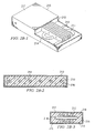
- FIGURE 1 is a perspective view of a plurality of electronic components 102 mounted on a coldplate 100 in accordance with one embodiment of the present invention. Any suitable method of coupling electronic components 102 to coldplate 100 is contemplated by the present invention.
- electronic components 102 are mounted on a circuit board 203 that is mounted on coldplate 100; however, the present invention contemplates electronic components 102 being directly mounted to coldplate 100.
- electronic components 102 comprise a high-powered phased array antenna system; however, electronic components 102 may comprise any suitable active electronically scanned array (“AESA”) or other suitable electronic systems having any suitable function.
- AESA active electronically scanned array
- Coldplate 100 may be any suitable substrate for mounting electronic components 102.
- One of the functions of coldplate 100 is to control thermal gradients and temperatures of electronic components 102 in order to ensure proper functioning of electronic components 102.
- Electronic components 102 sometimes have significant power dissipation, especially for phased array and other types of antenna systems.
- a cooling fluid may be circulated into coldplate 100 via an inlet 105.
- Any suitable fluid is contemplated by the present invention, such as ethylene glycol mixed with water or polyalphaolefin (“PAO”) or other suitable fluid.
- antenna systems such as the one illustrated in FIGURE 1
- aerospace applications such as military aircraft
- low weight is often a desired criteria along with low cost of manufacture.
- the type of material a particular coldplate is formed from is important with respect to thermal conductivity.
- coldplate 100 is formed from plastic in order to keep weight down. Any suitable polymer may be utilized for coldplate 100 and the subsequent coldplates illustrated in FIGURES 2A through 3B . As described in greater detail below in conjunction with FIGURES 2A through 3B , a highly conductive material or materials arc sometimes utilized along with a plastic coldplate to enhance the thermal management of electronic components 102.
- a highly conductive material as used herein is a material having a thermal conductivity of at least 5.0 W/m*K.
- a highly conductive material may be graphite, aluminum, or other suitable highly conductive material.
- FIGURES 2A through 2F are various views of a thermal management system for electronic components 102 utilizing a plastic coldplate according to various embodiments of the present invention.
- the embodiments illustrated in FIGURES 2A through 2F insert highly conductive material into plastic coldplates to facilitate the efficient transferring of heat from a surface of the coldplate to a cooling liquid.
- a plastic coldplate 200 includes one or more tubes 202 coupled to one or more enclosures 204.
- Coldplate 200 may be any suitable size and shape and may be formed using any suitable manufacturing method.
- Coldplate 200 has a mounting surface 201 for mounting electronic components thereto.
- Tubes 202 may also have any suitable size and shape and may be formed within coldplate 200 using any suitable method.
- tubes 202 are arranged within coldplate 200 in a boustrophedonic manner; however, any suitable configuration of tubes 202 are contemplated by the present invention.
- Tubes 202 are formed from a suitable highly conductive material, such as graphite or aluminum.
- Enclosures 204 may have any suitable size and shape and are also formed from any suitable highly conductive material.
- enclosures 204 are expanded portions of tube 202.
- Enclosures 204 have at least a portion that coincides with mounting surface 201 of coldplate 200.
- Enclosures 204 are positioned such that they correspond to respective portions of mounting surface 201 that have the highest heat-emitting electronic components thereon.
- a fluid flowing through tubes 202 and enclosures 204 may efficiently receive the heat generated by these high heat-emitting electronic components to control the thermal gradients within coldplate 200.
- a plastic coldplate 210 includes one or more tubes 214 coupled to a plurality of fins 212.
- Coldplate 210 is also housed within a housing 216 having a mounting surface 217 for mounting electronic components thereto.
- Coldplate 210 may be any suitable size and shape and may be formed using any suitable manufacturing method.
- Tubes 214 may also be any suitable size and shape and may be formed within coldplate 210 using any suitable manufacturing method. In a particular embodiment, tubes 214 arc arranged in a boustrophedonic manner; however, tubes 214 may be arranged within coldplate 210 in any suitable manner.
- Tubes 214 are formed from a suitable highly conductive material, such as graphite or aluminum.
- Fins 212 may be any suitable size and shape and are also formed from any suitable highly conductive material. Fins 212 may couple to tubes 214 in any suitable manner. In the illustrated embodiment, fins 212 are arranged vertically and parallel to one another; however, fins 212 may have any suitable arrangement. In one embodiment, fins 212 contact an upper inside surface 218 and a lower inside surface 219 of housing 216 in order to efficiently transfer the heat generated by electronic components on mounting surface 217 to a cooling liquid flowing through tubes 214 during operation. In other embodiments, fins 212 do not contact inside surface 218 and/or inside surface 219 of housing 216.
- Housing 216 may be any suitable size and shape and may be formed from any suitable highly conductive material. In one embodiment, housing 216 generally conforms to the outside configuration of coldplate 210. Referring to FIGURE 2C , a waffle panel 222 is disposed within an inner housing 223 and then disposed within a plastic coldplate 220. Coldplate 220 is, in turn, disposed within an outer housing 226 having a mounting surface 227 for mounting electronic components thereon.
- Waffle panel 222 and inner housing 223 may be of any suitable shape and may be formed from any suitable highly conductive material. Any suitable manufacturing method may be utilized to manufacture waffle panel 222 and inner housing 223.
- inner housing 223 includes a plurality of projections 224 that couple to an inside surface 229 of outer housing 226 in order to efficiently transfer heat from mounting surface 227 down into inner housing 223 in order to contact fluid flowing through waffle panel 222 during operation.
- projections 224 are positioned such that they correspond to respective portions 228 of mounting surface 227 that have the highest heat-emitting electronic components thereon.
- Coldplate 220 may have any suitable size and shape and may be formed using any suitable manufacturing method. Outer housing 226 may also have any suitable size and shape and generally conforms to the outside configuration of coldplate 220. Outer housing 226 may be formed from any suitable highly conductive material.
- a plastic coldplate 230 includes a waffle panel 232 disposed therein.
- Waffle panel 232 is similar to waffle panel 222 of FIGURE 2C and, hence, may be of any suitable shape and may be formed from any suitable highly conductive material using any suitable manufacturing method.
- waffle panel 232 contacts an inside surface 233 of coldplate 230 in order to efficiency transfer heat from mounting surface 231 throughout the interior of coldplate 230.
- Waffle panel 232 may also contact the other inside surfaces of coldplate 230 in other embodiments of the invention.
- Coldplate 230 may have any suitable size and shape and may be formed using any suitable manufacturing method.
- Coldplate 230 includes a mounting surface 231 for mounting electronic components thereto.
- a plastic coldplate 240 includes a plurality of passageways 246 formed therein.
- Coldplate 240 in the illustrated embodiment, is disposed within a housing 242 having a mounting surface 243 for mounting electronic components thereto.
- Housing 242 may be formed from any suitable highly conductive material.
- Coldplate 240 may have any suitable size and shape and may be formed using any suitable manufacturing method.
- coldplate 240 is formed from a top half 247 and a bottom half 248 in order to facilitate passageways 246 being separate from one another. Separate flowpaths (not illustrated) may be associated with each passageway 246 for a cooling liquid.
- Housing 242 may have a plurality of protrusions 244 extending from an upper inside surface 241 and a lower inside surface 249.
- Protrusions 244 in one embodiment, extend between adjacent passageways 246 in order to efficiently transfer heat from mounting surface 243 to a fluid flowing through each passageway 246.
- Protrusions 244 may have any suitable size and shape and may extend down into coldplate 240 any suitable distance. In other embodiments, protrusions 244 do not exist.
- a plastic coldplate 310 includes a plurality of vertical posts 314 disposed therein. Coldplate 310 is also disposed within a housing 312 having a mounting surface 313 for mounting electronic components thereto. Housing 312 may have any suitable size and shape and may be formed from any suitable highly conductive material.
- Coldplate 310 may be of any suitable size and shape and may be formed using any suitable manufacturing method.
- Vertical posts 314 may have any suitable size and shape and may be formed from any suitable highly conductive material. In the illustrated embodiment, vertical posts 314 couple to an upper inside surface 315 and a lower inside surface 316 of housing 312. In other embodiments, vertical posts 314 do not couple to upper inside surface 315 and/or lower inside surface 316.
- Vertical posts 314 may have any suitable arrangement and function to efficiently transfer heat emanating from electric components mounted on mounting surface 313 to a fluid flowing through coldplate 310.
- FIGURES 3A and 3B arc various views of a thermal management system for electronic components 102 utilizing a plastic coldplate according to other embodiments of the present invention.
- the embodiments illustrated in FIGURES 3A and 3B may utilize highly conductive material to efficiently spread the heat from electronic components throughout a volume of the plastic coldplate.
- a plastic coldplate 300 includes a plurality of fins 304 coupled to a plurality of heat pipes 306. Coldplate 300 is also disposed within a housing 302 having a mounting surface 303 for mounting electronic components thereto. Housing 302 may be any suitable size and shape and may be formed from any suitable highly conductive material.
- Coldplate 300 may be of any suitable size and shape and may be formed using any suitable manufacturing method. Fins 304 and heat pipes 306 are formed from any suitable highly conductive material and may be disposed within coldplate 300 in any suitable manner. In the illustrated embodiment, fins 304 and heat pipes 306 form a grid-like structure: however, the present invention contemplates any suitable arrangement for fins 304 and heat pipes 306. Fins 304 arc illustrated in FIGURE 3A as being vertically disposed and parallel to one another; however, fins 304 may have other configurations. In the illustrated embodiment, fins 304 contact an upper inside surface 307 and a lower inside surface 308 of housing 302. In other embodiments, fins 304 do not directly couple to upper inside surface 307 and/or lower inside surface 308. Heat pipes 306 may be any suitable heat pipes having any suitable configuration.
- a plastic coldplate 320 includes a plurality of vertical posts 324 and a plurality of horizontal fins 326. Coldplate 320 is also disposed within a housing 322 having a mounting surface 323 for mounting electronic components thereto. Housing 322 may have any suitable size and shape and may be formed from any suitable highly conductive material.
- Coldplate 320 may have any suitable size and shape and may be formed using any suitable manufacturing method.
- Vertical posts 324 arc similar to vertical posts 314 of FIGURE 2F and, hence, vertical posts 324 may couple to one or the other (or both) of an upper inside surface 327 or a lower inside surface 328 of housing 322.
- Horizontal fins 326 couple to vertical posts 324 and may be any suitable size and shape and may be formed from any suitable highly conductive material. In the illustrated embodiment, horizontal fins 326 are parallel spaced apart fins that couple to each vertical post 324. However, horizontal fins 326 may have any suitable arrangement. Horizontal fins 326 help facilitate efficient spreading of heat throughout a volume of coldplate 320.
- FIGURES 2A through 3B various embodiments of a thermal management system utilizing a plastic coldplate are illustrated in FIGURES 2A through 3B to efficiently control thermal gradients and temperatures within a particular coldplate.
- the plastic coldplates of the present invention help facilitate low weight and low cost for high-powered phased array antenna systems and other suitable electronic systems, which is especially important for aerospace applications.
- the thermal performance of plastic coldplates is enhanced by, in some embodiments, adding highly conductive material thereto as shown above in some of the embodiments in FIGURES 2A through 3B .
Abstract
Description
- This invention relates in general to thermal management of electronic equipment and, more particularly, to a thermal management system and method for electronic equipment mounted on coldplates.
- A trend for electronic equipment is lighter weight and lower cost. Lighter weight electronic equipment is especially important for aerospace applications, such as Active Electronically Scanned Arrays ("AESAs"). These AESAs often have significant power dissipation due to the type of electronic components involved. To control the thermal gradients and temperature of these systems, liquid flows through the coldplates to which they are attached may be utilized. These liquid cooled coldplates are typically formed from aluminum, which is a major contributor to the system weight rollup but possesses good thermal conductivity. Examples of plastic cold plate techniques can be found in
EP 0514141 andUS 6058013 . - According to a first aspect, the present invention provides a thermal management system for electronic components, comprising: a highly conductive housing having a mounting surface for mounting one or more electronic components; a plastic coldplate disposed within the highly conductive housing; and a highly conductive material disposed within the plastic coldplate and thermally coupled to the mounting surface, the highly conductive material operable to spread the heat throughout a volume of the plastic coldplate.
- The highly conductive material may comprise a plurality of vertical fins, the vertical fins coupled to a plurality of heat pipes. the highly conductive material may comprise a plurality of vertical posts coupled to the mounting surface. The vertical posts may further be coupled to a surface of the coldplate opposite the mounting surface. The highly conductive material may comprise a plurality of vertical posts coupled to a plurality of horizontal fins. The vertical posts may be couple to both the mounting surface and a surface of the coldplate opposite the mounting surface.
- According to a further aspect, the present invention provides a thermal management method for electronic components, comprising: mounting one or more electronic components on a mounting surface of a highly conductive housing; disposing a plastic coldplate within the highly conductive housing; disposing a highly conductive material within the plastic coldplate; and thermally coupling the highly conductive material to the mounting surface to spread the heat throughout a volume of the plastic coldplate.
- Mounting the one or more electronic components on the mounting surface of the highly conductive housing may comprise mounting the one or more electronic components on a circuit board and mounting the circuit board to the mounting surface. Thermally coupling the highly conductive material to the mounting surface may comprises coupling a plurality of vertical fins to the highly conductive housing and coupling the vertical fins to a plurality of heat pipes. Thermally coupling the highly conductive material to the mounting surface may comprise coupling a plurality of vertical posts to the mounting surface. Thermally coupling the highly conductive material to the mounting surface may comprise coupling a plurality of vertical posts to the highly conductive housing and coupling a plurality of horizontal fins to the vertical posts.
- According to a still further aspect, the present invention provides a thermal management system for electronic components, comprising: a plastic coldplate having a mounting surface for mounting one or more electronic components; one or more passageways disposed within the plastic coldplate, the passageways configured to have a fluid flow therethrough; and a highly conductive material disposed within the plastic coldplate and thermally coupled to the mounting surface, the highly conductive material operable to transfer heat from the mounting surface to the fluid flow.
- The electronic components may comprise an Active Electronically Scanned Array. A circuit board for mounting the one or more electronic components, the circuit board may be coupled to the mounting surface. The highly conductive material may comprise a waffle panel. The waffle panel may be disposed within a housing, the housing having one or more projections engaged with respective sections of the mounting surface. The plastic coldplate may be formed from two separate pieces and the passageways are separated from one another. The highly conductive material may comprise a plurality of protrusions extending between adjacent passageways. The one or more passageways may comprise a tube disposed within the plastic coldplate in a boustrophedonic manner and wherein the highly conductive material comprises a plurality of fins coupled to the tube. The one or more passageways may comprise one or more tubes disposed within the plastic coldplate and wherein the highly conductive material comprises one or more enclosures coupled to the tubes in series. The plastic coldplate may be housed within a highly conductive housing, the mounting surface associated with the housing. According to a still further aspect, the present invention provides a thermal management method for electronic components, comprising: mounting one or more electronic components on a mounting surface of a plastic coldplate, the plastic coldplate having one or more passageways disposed therein that arc configured to have a fluid flow therethrough: disposing a highly conductive material within the plastic coldplate; and thermally coupling the highly conductive material to the mounting surface to transfer heat from the mounting surface to the fluid flow during operation of the electronic components.
- Mounting the one or more electronic components on the mounting surface of the plastic coldplate may comprise mounting the one or more electronic components on a circuit board and mounting the circuit board to the mounting surface. Thermally coupling the highly conductive material to the mounting surface may comprises disposing a waffle panel within a housing and engaging one or more projections of the housing with respective portions of the mounting surface. The method may further comprise separating the passageways from one another. The method may further comprise housing the plastic coldplate within a highly conductive housing, the mounting surface associated with the housing.
- Embodiments of the invention provide a number of technical advantages. Embodiments of the invention may include all, some, or none of these advantages. For example, in one embodiment, forming coldplates of plastic materials enhances thermal performance, reduces weight, and lowers cost of high power phased array systems. Different techniques are utilized to efficiency move heat from the surface of a plastic coldplate into the cooling fluid. The techniques may be applicable to air, single phase liquid, and two phase (liquid/vapor) cooling. Some of the techniques of the present invention insert highly conductive material into the plastic coldplate to transfer the heat from the surface of the coldplate to the cooling liquid. Other may involve methods of efficiency transferring the heat into the cooling liquid itself.
- Other technical advantages are readily apparent to one skilled in the art from the following figures, descriptions, and claims.
-
-
FIGURE 1 is a perspective view of a plurality of electronic components mounted on a coldplate in accordance with an embodiment of the invention; -
FIGURES 2A through 2F are various views of a thermal management system for the coldplate ofFIGURE 1 according to some embodiments of the present invention; and -
FIGURES 3A and3B are various views of a thermal management system for the coldplate ofFIGURE 1 according to other embodiments of the present invention. - Embodiments of the present invention and some of their advantages are best understood by referring to
FIGURES 1 through 3B of the drawings, like numerals being used for like and corresponding parts of the various drawings. -
FIGURE 1 is a perspective view of a plurality ofelectronic components 102 mounted on acoldplate 100 in accordance with one embodiment of the present invention. Any suitable method of couplingelectronic components 102 tocoldplate 100 is contemplated by the present invention. In the illustrated embodiment,electronic components 102 are mounted on acircuit board 203 that is mounted oncoldplate 100; however, the present invention contemplateselectronic components 102 being directly mounted tocoldplate 100. In the illustrated embodiment,electronic components 102 comprise a high-powered phased array antenna system; however,electronic components 102 may comprise any suitable active electronically scanned array ("AESA") or other suitable electronic systems having any suitable function. - Coldplate 100 may be any suitable substrate for mounting
electronic components 102. One of the functions ofcoldplate 100 is to control thermal gradients and temperatures ofelectronic components 102 in order to ensure proper functioning ofelectronic components 102.Electronic components 102 sometimes have significant power dissipation, especially for phased array and other types of antenna systems. To control the thermal gradients and temperature ofelectronic components 102, a cooling fluid may be circulated intocoldplate 100 via an inlet 105. Any suitable fluid is contemplated by the present invention, such as ethylene glycol mixed with water or polyalphaolefin ("PAO") or other suitable fluid. - Because antenna systems, such as the one illustrated in
FIGURE 1 , are oftentimes utilized in aerospace applications, such as military aircraft, low weight is often a desired criteria along with low cost of manufacture. However, because of the thermal considerations, the type of material a particular coldplate is formed from is important with respect to thermal conductivity. - Therefore, according to the teachings of one embodiment of the present invention,
coldplate 100 is formed from plastic in order to keep weight down. Any suitable polymer may be utilized forcoldplate 100 and the subsequent coldplates illustrated inFIGURES 2A through 3B . As described in greater detail below in conjunction withFIGURES 2A through 3B , a highly conductive material or materials arc sometimes utilized along with a plastic coldplate to enhance the thermal management ofelectronic components 102. A highly conductive material as used herein is a material having a thermal conductivity of at least 5.0 W/m*K. For example, a highly conductive material may be graphite, aluminum, or other suitable highly conductive material. Various embodiments of thermal management systems using a plastic coldplate are shown and described below in conjunction withFIGURES 2A through 3B . -
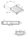
FIGURES 2A through 2F are various views of a thermal management system forelectronic components 102 utilizing a plastic coldplate according to various embodiments of the present invention. Generally, the embodiments illustrated inFIGURES 2A through 2F insert highly conductive material into plastic coldplates to facilitate the efficient transferring of heat from a surface of the coldplate to a cooling liquid. - Referring to
FIGURE 2A , aplastic coldplate 200 includes one ormore tubes 202 coupled to one ormore enclosures 204.Coldplate 200 may be any suitable size and shape and may be formed using any suitable manufacturing method.Coldplate 200 has a mountingsurface 201 for mounting electronic components thereto.Tubes 202 may also have any suitable size and shape and may be formed withincoldplate 200 using any suitable method. In a particular embodiment,tubes 202 are arranged withincoldplate 200 in a boustrophedonic manner; however, any suitable configuration oftubes 202 are contemplated by the present invention.Tubes 202 are formed from a suitable highly conductive material, such as graphite or aluminum. -
Enclosures 204 may have any suitable size and shape and are also formed from any suitable highly conductive material. In a particular embodiment,enclosures 204 are expanded portions oftube 202.Enclosures 204 have at least a portion that coincides with mountingsurface 201 ofcoldplate 200.Enclosures 204 are positioned such that they correspond to respective portions of mountingsurface 201 that have the highest heat-emitting electronic components thereon. Thus, a fluid flowing throughtubes 202 andenclosures 204 may efficiently receive the heat generated by these high heat-emitting electronic components to control the thermal gradients withincoldplate 200. - Referring to
FIGURE 2B , aplastic coldplate 210 includes one ormore tubes 214 coupled to a plurality offins 212.Coldplate 210 is also housed within ahousing 216 having a mountingsurface 217 for mounting electronic components thereto.Coldplate 210 may be any suitable size and shape and may be formed using any suitable manufacturing method.Tubes 214 may also be any suitable size and shape and may be formed withincoldplate 210 using any suitable manufacturing method. In a particular embodiment,tubes 214 arc arranged in a boustrophedonic manner; however,tubes 214 may be arranged withincoldplate 210 in any suitable manner.Tubes 214 are formed from a suitable highly conductive material, such as graphite or aluminum. -
Fins 212 may be any suitable size and shape and are also formed from any suitable highly conductive material.Fins 212 may couple totubes 214 in any suitable manner. In the illustrated embodiment,fins 212 are arranged vertically and parallel to one another; however,fins 212 may have any suitable arrangement. In one embodiment,fins 212 contact an upperinside surface 218 and a lower insidesurface 219 ofhousing 216 in order to efficiently transfer the heat generated by electronic components on mountingsurface 217 to a cooling liquid flowing throughtubes 214 during operation. In other embodiments,fins 212 do not contact insidesurface 218 and/or insidesurface 219 ofhousing 216. -
Housing 216 may be any suitable size and shape and may be formed from any suitable highly conductive material. In one embodiment,housing 216 generally conforms to the outside configuration ofcoldplate 210. Referring toFIGURE 2C , awaffle panel 222 is disposed within aninner housing 223 and then disposed within aplastic coldplate 220.Coldplate 220 is, in turn, disposed within anouter housing 226 having a mountingsurface 227 for mounting electronic components thereon. -
Waffle panel 222 andinner housing 223 may be of any suitable shape and may be formed from any suitable highly conductive material. Any suitable manufacturing method may be utilized to manufacturewaffle panel 222 andinner housing 223. In one embodiment,inner housing 223 includes a plurality ofprojections 224 that couple to aninside surface 229 ofouter housing 226 in order to efficiently transfer heat from mountingsurface 227 down intoinner housing 223 in order to contact fluid flowing throughwaffle panel 222 during operation. In one embodiment,projections 224 are positioned such that they correspond torespective portions 228 of mountingsurface 227 that have the highest heat-emitting electronic components thereon. -
Coldplate 220 may have any suitable size and shape and may be formed using any suitable manufacturing method.Outer housing 226 may also have any suitable size and shape and generally conforms to the outside configuration ofcoldplate 220.Outer housing 226 may be formed from any suitable highly conductive material. - Referring to
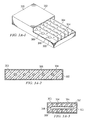
FIGURE 2D , aplastic coldplate 230 includes awaffle panel 232 disposed therein.Waffle panel 232 is similar towaffle panel 222 ofFIGURE 2C and, hence, may be of any suitable shape and may be formed from any suitable highly conductive material using any suitable manufacturing method. In one embodiment,waffle panel 232 contacts aninside surface 233 ofcoldplate 230 in order to efficiency transfer heat from mountingsurface 231 throughout the interior ofcoldplate 230.Waffle panel 232 may also contact the other inside surfaces ofcoldplate 230 in other embodiments of the invention. -
Coldplate 230 may have any suitable size and shape and may be formed using any suitable manufacturing method.Coldplate 230 includes a mountingsurface 231 for mounting electronic components thereto. - Referring to
FIGURE 2E , aplastic coldplate 240 includes a plurality ofpassageways 246 formed therein.Coldplate 240, in the illustrated embodiment, is disposed within ahousing 242 having a mountingsurface 243 for mounting electronic components thereto.Housing 242 may be formed from any suitable highly conductive material. -
Coldplate 240 may have any suitable size and shape and may be formed using any suitable manufacturing method. In a particular embodiment,coldplate 240 is formed from atop half 247 and abottom half 248 in order to facilitatepassageways 246 being separate from one another. Separate flowpaths (not illustrated) may be associated with eachpassageway 246 for a cooling liquid. -
Housing 242 may have a plurality ofprotrusions 244 extending from an upperinside surface 241 and a lower insidesurface 249.Protrusions 244, in one embodiment, extend betweenadjacent passageways 246 in order to efficiently transfer heat from mountingsurface 243 to a fluid flowing through eachpassageway 246.Protrusions 244 may have any suitable size and shape and may extend down intocoldplate 240 any suitable distance. In other embodiments,protrusions 244 do not exist. - Referring to
FIGURE 2F , aplastic coldplate 310 includes a plurality ofvertical posts 314 disposed therein.Coldplate 310 is also disposed within ahousing 312 having a mountingsurface 313 for mounting electronic components thereto.Housing 312 may have any suitable size and shape and may be formed from any suitable highly conductive material. -
Coldplate 310 may be of any suitable size and shape and may be formed using any suitable manufacturing method.Vertical posts 314 may have any suitable size and shape and may be formed from any suitable highly conductive material. In the illustrated embodiment,vertical posts 314 couple to an upperinside surface 315 and a lower insidesurface 316 ofhousing 312. In other embodiments,vertical posts 314 do not couple to upper insidesurface 315 and/or lower insidesurface 316.Vertical posts 314 may have any suitable arrangement and function to efficiently transfer heat emanating from electric components mounted on mountingsurface 313 to a fluid flowing throughcoldplate 310. -
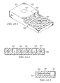
FIGURES 3A and3B arc various views of a thermal management system forelectronic components 102 utilizing a plastic coldplate according to other embodiments of the present invention. The embodiments illustrated inFIGURES 3A and3B may utilize highly conductive material to efficiently spread the heat from electronic components throughout a volume of the plastic coldplate. - Referring to
FIGURE 3A , aplastic coldplate 300 includes a plurality offins 304 coupled to a plurality ofheat pipes 306.Coldplate 300 is also disposed within ahousing 302 having a mountingsurface 303 for mounting electronic components thereto.Housing 302 may be any suitable size and shape and may be formed from any suitable highly conductive material. -
Coldplate 300 may be of any suitable size and shape and may be formed using any suitable manufacturing method.Fins 304 andheat pipes 306 are formed from any suitable highly conductive material and may be disposed withincoldplate 300 in any suitable manner. In the illustrated embodiment,fins 304 andheat pipes 306 form a grid-like structure: however, the present invention contemplates any suitable arrangement forfins 304 andheat pipes 306.Fins 304 arc illustrated inFIGURE 3A as being vertically disposed and parallel to one another; however,fins 304 may have other configurations. In the illustrated embodiment,fins 304 contact an upperinside surface 307 and a lower insidesurface 308 ofhousing 302. In other embodiments,fins 304 do not directly couple to upper insidesurface 307 and/or lower insidesurface 308.Heat pipes 306 may be any suitable heat pipes having any suitable configuration. - Referring to
FIGURE 3B , aplastic coldplate 320 includes a plurality ofvertical posts 324 and a plurality ofhorizontal fins 326.Coldplate 320 is also disposed within ahousing 322 having a mountingsurface 323 for mounting electronic components thereto.Housing 322 may have any suitable size and shape and may be formed from any suitable highly conductive material. -
Coldplate 320 may have any suitable size and shape and may be formed using any suitable manufacturing method.Vertical posts 324 arc similar tovertical posts 314 ofFIGURE 2F and, hence,vertical posts 324 may couple to one or the other (or both) of an upperinside surface 327 or a lower insidesurface 328 ofhousing 322.Horizontal fins 326 couple tovertical posts 324 and may be any suitable size and shape and may be formed from any suitable highly conductive material. In the illustrated embodiment,horizontal fins 326 are parallel spaced apart fins that couple to eachvertical post 324. However,horizontal fins 326 may have any suitable arrangement.Horizontal fins 326 help facilitate efficient spreading of heat throughout a volume ofcoldplate 320. - Thus, various embodiments of a thermal management system utilizing a plastic coldplate are illustrated in
FIGURES 2A through 3B to efficiently control thermal gradients and temperatures within a particular coldplate. The plastic coldplates of the present invention help facilitate low weight and low cost for high-powered phased array antenna systems and other suitable electronic systems, which is especially important for aerospace applications. In addition, the thermal performance of plastic coldplates is enhanced by, in some embodiments, adding highly conductive material thereto as shown above in some of the embodiments inFIGURES 2A through 3B .
Claims (11)
- A thermal management system for electronic components (102), comprising:a highly conductive housing (302) having a mounting surface (303;313;323) for mounting one or more electronic components (102);a plastic coldplate (300;310;320) disposed within the highly conductive housing (302); anda highly conductive material disposed within the plastic coldplate and thermally coupled to the mounting surface, the highly conductive material operable to spread the heat throughout a volume of the plastic coldplate, characterised in that the highly conductive material comprises a plurality of vertical fins (304), the vertical fins coupled to a plurality of heat pipes (306).
- The system of claim 1, further comprising a circuit board for mounting the one or more electronic components, the circuit board coupled to the mounting surface.
- The system of claim 1, wherein the highly conductive material comprises a plurality of vertical posts (314) coupled to the mounting surface (313).
- The system of claim 3, wherein the vertical posts (314) are further coupled to a surface (316) of the coldplate (310) opposite the mounting surface (316).
- The system of claim 1, wherein the highly conductive material comprises a plurality of vertical posts (324) coupled to a plurality of horizontal fins (326).
- The system of claim 5, wherein the vertical posts (324) couple to both the mounting surface (323) and a surface (328) of the coldplate (320) opposite the mounting surface (323).
- A thermal management method for electronic components (102), comprising:mounting one or more electronic components (102) on a mounting surface (201;217;227;231;243;303;313;323) of a highly conductive housing;disposing a plastic coldplate (100;200;210;220;230;240;300;310; 320) within the highly conductive housing;disposing a highly conductive material within the plastic coldplate; andthermally coupling the highly conductive material to the mounting surface to spread the heat throughout a volume of the plastic coldplatethe method being characterised in that, thermally coupling the highly conductive material to the mounting surface (303) comprises coupling a plurality of vertical fins (304) to the highly conductive housing and coupling the vertical fins (304) to a plurality of heat pipes (306).
- The method of claim 7, wherein mounting the one or more electronic components (102) on the mounting surface (201;217;227;231;243;303;313;323) of the highly conductive housing comprises mounting the one or more electronic components (102) on a circuit board (203) and mounting the circuit board (323) to the mounting surface.
- The method of claim 7 or claim 8, wherein mounting the one or more electronic components on the mounting surface of the highly conductive housing comprises mounting the one or more electronic components on a circuit board and mounting the circuit board to the mounting surface.
- The method of any one of claims 7 to 9, wherein thermally coupling the highly conductive material to the mounting surface (313) comprises coupling a plurality of vertical posts (314) to the mounting surface (313).
- The method of any one of claims 7 to 10, wherein thermally coupling the highly conductive material to the mounting surface (323) comprises coupling a plurality of vertical posts (324) to the highly conductive housing and coupling a plurality of horizontal fins (326) to the vertical posts (324).
Applications Claiming Priority (2)
| Application Number | Priority Date | Filing Date | Title |
|---|---|---|---|
| US10/848,336 US6989991B2 (en) | 2004-05-18 | 2004-05-18 | Thermal management system and method for electronic equipment mounted on coldplates |
| EP05253019A EP1599081B1 (en) | 2004-05-18 | 2005-05-17 | Thermal management system and method for electronic equipment mounted on coldplates |
Related Parent Applications (2)
| Application Number | Title | Priority Date | Filing Date |
|---|---|---|---|
| EP05253019.3 Division | 2005-05-17 | ||
| EP05253019A Division EP1599081B1 (en) | 2004-05-18 | 2005-05-17 | Thermal management system and method for electronic equipment mounted on coldplates |
Publications (3)
| Publication Number | Publication Date |
|---|---|
| EP2112875A2 EP2112875A2 (en) | 2009-10-28 |
| EP2112875A3 EP2112875A3 (en) | 2009-12-02 |
| EP2112875B1 true EP2112875B1 (en) | 2012-05-16 |
Family
ID=34941340
Family Applications (2)
| Application Number | Title | Priority Date | Filing Date |
|---|---|---|---|
| EP05253019A Active EP1599081B1 (en) | 2004-05-18 | 2005-05-17 | Thermal management system and method for electronic equipment mounted on coldplates |
| EP09165347A Active EP2112875B1 (en) | 2004-05-18 | 2005-05-17 | Thermal management system and method for electronic equipment mounted on coldplates |
Family Applications Before (1)
| Application Number | Title | Priority Date | Filing Date |
|---|---|---|---|
| EP05253019A Active EP1599081B1 (en) | 2004-05-18 | 2005-05-17 | Thermal management system and method for electronic equipment mounted on coldplates |
Country Status (4)
| Country | Link |
|---|---|
| US (2) | US6989991B2 (en) |
| EP (2) | EP1599081B1 (en) |
| AT (1) | ATE516695T1 (en) |
| ES (1) | ES2367695T3 (en) |
Families Citing this family (43)
| Publication number | Priority date | Publication date | Assignee | Title |
|---|---|---|---|---|
| DE102004026061B4 (en) * | 2004-05-25 | 2009-09-10 | Danfoss Silicon Power Gmbh | Power semiconductor module and method for cooling a power semiconductor module |
| US7983042B2 (en) * | 2004-06-15 | 2011-07-19 | Raytheon Company | Thermal management system and method for thin membrane type antennas |
| US7168152B1 (en) * | 2004-10-18 | 2007-01-30 | Lockheed Martin Corporation | Method for making an integrated active antenna element |
| US7677299B2 (en) * | 2004-11-10 | 2010-03-16 | Wen-Chun Zheng | Nearly isothermal heat pipe heat sink |
| US7292439B2 (en) * | 2005-01-19 | 2007-11-06 | Raytheon Company | Thermal management system and method for electronic assemblies |
| US7511372B2 (en) * | 2005-06-28 | 2009-03-31 | Intel Corporation | Microelectronic die cooling device including bonding posts and method of forming same |
| US7443354B2 (en) * | 2005-08-09 | 2008-10-28 | The Boeing Company | Compliant, internally cooled antenna apparatus and method |
| US7624791B2 (en) * | 2006-09-08 | 2009-12-01 | Advanced Energy Industries, Inc. | Cooling apparatus for electronics |
| US7551440B2 (en) * | 2007-01-24 | 2009-06-23 | Hewlett-Packard Development Company, L.P. | System and method for cooling an electronic component |
| DK2143139T3 (en) * | 2007-04-26 | 2019-09-23 | Ceram Gmbh | REFRIGERATOR BOX FOR COMPONENTS OR CIRCUITS |
| US7940524B2 (en) * | 2007-10-01 | 2011-05-10 | Raytheon Company | Remote cooling of a phased array antenna |
| US8002021B1 (en) * | 2008-02-04 | 2011-08-23 | Advanced Cooling Technologies, Inc. | Heat exchanger with internal heat pipe |
| US8503941B2 (en) | 2008-02-21 | 2013-08-06 | The Boeing Company | System and method for optimized unmanned vehicle communication using telemetry |
| TW201036527A (en) * | 2009-03-19 | 2010-10-01 | Acbel Polytech Inc | Large-area liquid-cooled heat-dissipation device |
| EP2259310B1 (en) * | 2009-06-05 | 2020-04-08 | Siemens Gamesa Renewable Energy A/S | Integrated heat exchanger |
| US8222541B2 (en) * | 2009-06-19 | 2012-07-17 | General Electric Company | Avionics chassis |
| US8023267B2 (en) * | 2009-06-19 | 2011-09-20 | General Electric Company | Avionics chassis |
| US7911796B2 (en) * | 2009-06-19 | 2011-03-22 | General Electric Company | Avionics chassis |
| US8059409B2 (en) * | 2009-06-19 | 2011-11-15 | General Electric Company | Avionics chassis |
| US20110056669A1 (en) * | 2009-09-04 | 2011-03-10 | Raytheon Company | Heat Transfer Device |
| US20120026692A1 (en) | 2010-07-28 | 2012-02-02 | Wolverine Tube, Inc. | Electronics substrate with enhanced direct bonded metal |
| US9795057B2 (en) | 2010-07-28 | 2017-10-17 | Wolverine Tube, Inc. | Method of producing a liquid cooled coldplate |
| US10531594B2 (en) | 2010-07-28 | 2020-01-07 | Wieland Microcool, Llc | Method of producing a liquid cooled coldplate |
| FR2979048B1 (en) * | 2011-08-08 | 2015-03-20 | Valeo Sys Controle Moteur Sas | DEVICE COMPRISING A BODY HAVING A RECEPTION SURFACE OF AT LEAST ONE ELECTRONIC COMPONENT AND A CONDUIT THAT CAN RECEIVE A COOLING FLUID |
| EP2752104B1 (en) | 2011-09-02 | 2022-05-04 | Wieland Microcool, LLC | Enhanced clad metal base plate assembly |
| US9255741B2 (en) * | 2012-01-26 | 2016-02-09 | Lear Corporation | Cooled electric assembly |
| DE102013212724B3 (en) * | 2013-06-28 | 2014-12-04 | TRUMPF Hüttinger GmbH + Co. KG | Cooling device for cooling an electronic component and electronic assembly with a cooling device |
| US9468131B2 (en) * | 2014-04-16 | 2016-10-11 | Raytheon Company | Monolithic multi-module electronics chassis with multi-planar embedded fluid cooling channels |
| US9345169B1 (en) | 2014-11-18 | 2016-05-17 | International Business Machines Corporation | Liquid-cooled heat sink assemblies |
| US9865522B2 (en) | 2014-11-18 | 2018-01-09 | International Business Machines Corporation | Composite heat sink structures |
| US10265812B2 (en) | 2015-08-12 | 2019-04-23 | International Business Machines Corporation | Liquid-cooled, composite heat sink assemblies |
| PL3162731T3 (en) * | 2015-10-30 | 2019-03-29 | Ecolean Ab | Pouch type package and associated method for adapatation of such a package |
| DE102016214965A1 (en) * | 2016-08-11 | 2018-02-15 | Siemens Aktiengesellschaft | Temperature control unit for a circuit carrier, method for their preparation and method for determining the geometry of a temperature control unit |
| JP7269176B2 (en) | 2017-03-21 | 2023-05-08 | エルジー イノテック カンパニー リミテッド | converter |
| US10840573B2 (en) | 2017-12-05 | 2020-11-17 | The United States Of America, As Represented By The Secretary Of The Air Force | Linear-to-circular polarizers using cascaded sheet impedances and cascaded waveplates |
| US10547117B1 (en) | 2017-12-05 | 2020-01-28 | Unites States Of America As Represented By The Secretary Of The Air Force | Millimeter wave, wideband, wide scan phased array architecture for radiating circular polarization at high power levels |
| US10433458B1 (en) * | 2018-05-08 | 2019-10-01 | Hewlett Packard Enterprise Development Lp | Conducting plastic cold plates |
| CN110146956B (en) * | 2019-04-25 | 2021-04-27 | 东南大学 | Internal heat transport microstructure of optical module |
| CN110113867B (en) * | 2019-05-31 | 2021-03-02 | 维沃移动通信有限公司 | Heat radiation structure and mobile terminal |
| US11252811B2 (en) * | 2020-01-15 | 2022-02-15 | Cisco Technology, Inc. | Power distribution from point-of-load with cooling |
| US11270925B2 (en) | 2020-05-28 | 2022-03-08 | Google Llc | Heat distribution device with flow channels |
| DE102021104390A1 (en) | 2021-02-24 | 2022-08-25 | Scherdel Innotec Forschungs- Und Entwicklungs-Gmbh | Injection molded housing, power electronic component and thermal management element therewith and method for producing an injection molded housing |
| FR3122547A1 (en) * | 2021-04-29 | 2022-11-04 | Valeo Siemens Eautomotive France Sas | Cooling module including a cooling structure for heat dissipation |
Family Cites Families (21)
| Publication number | Priority date | Publication date | Assignee | Title |
|---|---|---|---|---|
| JPH03274796A (en) * | 1990-03-23 | 1991-12-05 | Koufu Nippon Denki Kk | Cold plate mechanism |
| US5159529A (en) * | 1991-05-15 | 1992-10-27 | International Business Machines Corporation | Composite liquid cooled plate for electronic equipment |
| US5453911A (en) * | 1994-02-17 | 1995-09-26 | General Motors Corporation | Device for cooling power electronics |
| US6184832B1 (en) | 1996-05-17 | 2001-02-06 | Raytheon Company | Phased array antenna |
| DE19643717A1 (en) * | 1996-10-23 | 1998-04-30 | Asea Brown Boveri | Liquid cooling device for a high-performance semiconductor module |
| JP3082738B2 (en) * | 1998-03-13 | 2000-08-28 | 日本電気株式会社 | High efficiency liquid cooling device |
| US6058013A (en) * | 1998-07-02 | 2000-05-02 | Motorola Inc. | Molded housing with integral heatsink |
| US6219237B1 (en) * | 1998-08-31 | 2001-04-17 | Micron Technology, Inc. | Structure and method for an electronic assembly |
| US6016007A (en) * | 1998-10-16 | 2000-01-18 | Northrop Grumman Corp. | Power electronics cooling apparatus |
| US6297775B1 (en) | 1999-09-16 | 2001-10-02 | Raytheon Company | Compact phased array antenna system, and a method of operating same |
| DE10006215A1 (en) * | 2000-02-11 | 2001-08-16 | Abb Semiconductors Ag Baden | Cooling device for a high-performance semiconductor module |
| FR2809281B1 (en) * | 2000-05-22 | 2002-07-12 | Alstom | ELECTRONIC POWER DEVICE |
| US7017651B1 (en) * | 2000-09-13 | 2006-03-28 | Raytheon Company | Method and apparatus for temperature gradient control in an electronic system |
| JP4423792B2 (en) * | 2000-09-14 | 2010-03-03 | 株式会社デンソー | Boiling cooler |
| US6578626B1 (en) * | 2000-11-21 | 2003-06-17 | Thermal Corp. | Liquid cooled heat exchanger with enhanced flow |
| JP3946018B2 (en) * | 2001-09-18 | 2007-07-18 | 株式会社日立製作所 | Liquid-cooled circuit device |
| US6679315B2 (en) * | 2002-01-14 | 2004-01-20 | Marconi Communications, Inc. | Small scale chip cooler assembly |
| US6819561B2 (en) * | 2002-02-22 | 2004-11-16 | Satcon Technology Corporation | Finned-tube heat exchangers and cold plates, self-cooling electronic component systems using same, and methods for cooling electronic components using same |
| US6591898B1 (en) * | 2002-06-20 | 2003-07-15 | International Business Machines Corporation | Integrated heat sink system for a closed electronics container |
| DE10246990A1 (en) * | 2002-10-02 | 2004-04-22 | Atotech Deutschland Gmbh | Microstructure cooler and its use |
| US20050128705A1 (en) * | 2003-12-16 | 2005-06-16 | International Business Machines Corporation | Composite cold plate assembly |
-
2004
- 2004-05-18 US US10/848,336 patent/US6989991B2/en active Active
-
2005
- 2005-05-17 AT AT05253019T patent/ATE516695T1/en not_active IP Right Cessation
- 2005-05-17 ES ES05253019T patent/ES2367695T3/en active Active
- 2005-05-17 EP EP05253019A patent/EP1599081B1/en active Active
- 2005-05-17 EP EP09165347A patent/EP2112875B1/en active Active
- 2005-12-13 US US11/301,567 patent/US7092255B2/en active Active
Also Published As
| Publication number | Publication date |
|---|---|
| EP2112875A2 (en) | 2009-10-28 |
| US7092255B2 (en) | 2006-08-15 |
| ATE516695T1 (en) | 2011-07-15 |
| US20060098410A1 (en) | 2006-05-11 |
| EP1599081B1 (en) | 2011-07-13 |
| EP1599081A2 (en) | 2005-11-23 |
| US20050259396A1 (en) | 2005-11-24 |
| ES2367695T3 (en) | 2011-11-07 |
| EP2112875A3 (en) | 2009-12-02 |
| EP1599081A3 (en) | 2007-05-23 |
| US6989991B2 (en) | 2006-01-24 |
Similar Documents
| Publication | Publication Date | Title |
|---|---|---|
| EP2112875B1 (en) | Thermal management system and method for electronic equipment mounted on coldplates | |
| EP2031332B1 (en) | Heat exchanger for power-electronics components | |
| CN104509220B (en) | Lid is heated seal including protectiveness and optimizes the thermoelectric heat exchanger component of interface resistance | |
| EP2170030B1 (en) | Electronic apparatus | |
| EP2525632B1 (en) | Systems for circuit board heat transfer and method of assembling same | |
| EP2814089B1 (en) | Battery pack with a bus bar having novel structure | |
| US6292364B1 (en) | Liquid spray cooled module | |
| US20030205363A1 (en) | Enhanced air cooling of electronic devices using fluid phase change heat transfer | |
| US20030221814A1 (en) | Apparatus having forced fluid cooling and pin-fin heat sink | |
| US20050018407A1 (en) | Stack up assembly | |
| TR201815693T4 (en) | Thermally and electrically conductive apparatus. | |
| WO2014106051A1 (en) | Heat sink apparatus and method for power semiconductor device module | |
| CN111213439A (en) | Electronic device | |
| EP2552182A1 (en) | Double-loop thermosiphon for cooling of electric and electronic components | |
| JP2000161880A (en) | Heat pipe type cooler | |
| JPH02201999A (en) | Cooling plane device for cooling electronic circuit parts | |
| EP2383779B1 (en) | Mounting base | |
| CN210534699U (en) | Heat dissipation module structure for server | |
| EP0645593A1 (en) | Electronic cooling type refrigerator | |
| CN110679207B (en) | Cooling device | |
| US7111666B2 (en) | Heat sink | |
| US11864357B2 (en) | Double-sided cooling cold plates with overhanging heat sinks and through body busbar for high-power density power electronics | |
| US7929306B2 (en) | Circuit pack cooling solution | |
| CN217985855U (en) | Phase change heat sink and electronic device having the same | |
| JP2015170943A (en) | Electronic device |
Legal Events
| Date | Code | Title | Description |
|---|---|---|---|
| PUAI | Public reference made under article 153(3) epc to a published international application that has entered the european phase |
Free format text: ORIGINAL CODE: 0009012 |
|
| 17P | Request for examination filed |
Effective date: 20090811 |
|
| AC | Divisional application: reference to earlier application |
Ref document number: 1599081 Country of ref document: EP Kind code of ref document: P |
|
| AK | Designated contracting states |
Kind code of ref document: A2 Designated state(s): AT BE BG CH CY CZ DE DK EE ES FI FR GB GR HU IE IS IT LI LT LU MC NL PL PT RO SE SI SK TR |
|
| PUAL | Search report despatched |
Free format text: ORIGINAL CODE: 0009013 |
|
| AK | Designated contracting states |
Kind code of ref document: A3 Designated state(s): AT BE BG CH CY CZ DE DK EE ES FI FR GB GR HU IE IS IT LI LT LU MC NL PL PT RO SE SI SK TR |
|
| 17Q | First examination report despatched |
Effective date: 20100127 |
|
| GRAP | Despatch of communication of intention to grant a patent |
Free format text: ORIGINAL CODE: EPIDOSNIGR1 |
|
| GRAS | Grant fee paid |
Free format text: ORIGINAL CODE: EPIDOSNIGR3 |
|
| GRAA | (expected) grant |
Free format text: ORIGINAL CODE: 0009210 |
|
| AC | Divisional application: reference to earlier application |
Ref document number: 1599081 Country of ref document: EP Kind code of ref document: P |
|
| AK | Designated contracting states |
Kind code of ref document: B1 Designated state(s): AT BE BG CH CY CZ DE DK EE ES FI FR GB GR HU IE IS IT LI LT LU MC NL PL PT RO SE SI SK TR |
|
| REG | Reference to a national code |
Ref country code: GB Ref legal event code: FG4D |
|
| REG | Reference to a national code |
Ref country code: CH Ref legal event code: EP |
|
| REG | Reference to a national code |
Ref country code: AT Ref legal event code: REF Ref document number: 558598 Country of ref document: AT Kind code of ref document: T Effective date: 20120615 |
|
| REG | Reference to a national code |
Ref country code: IE Ref legal event code: FG4D |
|
| REG | Reference to a national code |
Ref country code: DE Ref legal event code: R096 Ref document number: 602005034256 Country of ref document: DE Effective date: 20120712 |
|
| REG | Reference to a national code |
Ref country code: NL Ref legal event code: VDEP Effective date: 20120516 |
|
| REG | Reference to a national code |
Ref country code: LT Ref legal event code: MG4D Effective date: 20120516 |
|
| PG25 | Lapsed in a contracting state [announced via postgrant information from national office to epo] |
Ref country code: FI Free format text: LAPSE BECAUSE OF FAILURE TO SUBMIT A TRANSLATION OF THE DESCRIPTION OR TO PAY THE FEE WITHIN THE PRESCRIBED TIME-LIMIT Effective date: 20120516 Ref country code: LT Free format text: LAPSE BECAUSE OF FAILURE TO SUBMIT A TRANSLATION OF THE DESCRIPTION OR TO PAY THE FEE WITHIN THE PRESCRIBED TIME-LIMIT Effective date: 20120516 Ref country code: CY Free format text: LAPSE BECAUSE OF FAILURE TO SUBMIT A TRANSLATION OF THE DESCRIPTION OR TO PAY THE FEE WITHIN THE PRESCRIBED TIME-LIMIT Effective date: 20120516 Ref country code: PL Free format text: LAPSE BECAUSE OF FAILURE TO SUBMIT A TRANSLATION OF THE DESCRIPTION OR TO PAY THE FEE WITHIN THE PRESCRIBED TIME-LIMIT Effective date: 20120516 Ref country code: SE Free format text: LAPSE BECAUSE OF FAILURE TO SUBMIT A TRANSLATION OF THE DESCRIPTION OR TO PAY THE FEE WITHIN THE PRESCRIBED TIME-LIMIT Effective date: 20120516 Ref country code: IS Free format text: LAPSE BECAUSE OF FAILURE TO SUBMIT A TRANSLATION OF THE DESCRIPTION OR TO PAY THE FEE WITHIN THE PRESCRIBED TIME-LIMIT Effective date: 20120916 |
|
| REG | Reference to a national code |
Ref country code: AT Ref legal event code: MK05 Ref document number: 558598 Country of ref document: AT Kind code of ref document: T Effective date: 20120516 |
|
| PG25 | Lapsed in a contracting state [announced via postgrant information from national office to epo] |
Ref country code: GR Free format text: LAPSE BECAUSE OF FAILURE TO SUBMIT A TRANSLATION OF THE DESCRIPTION OR TO PAY THE FEE WITHIN THE PRESCRIBED TIME-LIMIT Effective date: 20120817 Ref country code: SI Free format text: LAPSE BECAUSE OF FAILURE TO SUBMIT A TRANSLATION OF THE DESCRIPTION OR TO PAY THE FEE WITHIN THE PRESCRIBED TIME-LIMIT Effective date: 20120516 Ref country code: PT Free format text: LAPSE BECAUSE OF FAILURE TO SUBMIT A TRANSLATION OF THE DESCRIPTION OR TO PAY THE FEE WITHIN THE PRESCRIBED TIME-LIMIT Effective date: 20120917 |
|
| PG25 | Lapsed in a contracting state [announced via postgrant information from national office to epo] |
Ref country code: BE Free format text: LAPSE BECAUSE OF FAILURE TO SUBMIT A TRANSLATION OF THE DESCRIPTION OR TO PAY THE FEE WITHIN THE PRESCRIBED TIME-LIMIT Effective date: 20120516 Ref country code: MC Free format text: LAPSE BECAUSE OF NON-PAYMENT OF DUE FEES Effective date: 20120531 |
|
| REG | Reference to a national code |
Ref country code: CH Ref legal event code: PL |
|
| PG25 | Lapsed in a contracting state [announced via postgrant information from national office to epo] |
Ref country code: SK Free format text: LAPSE BECAUSE OF FAILURE TO SUBMIT A TRANSLATION OF THE DESCRIPTION OR TO PAY THE FEE WITHIN THE PRESCRIBED TIME-LIMIT Effective date: 20120516 Ref country code: CH Free format text: LAPSE BECAUSE OF NON-PAYMENT OF DUE FEES Effective date: 20120531 Ref country code: LI Free format text: LAPSE BECAUSE OF NON-PAYMENT OF DUE FEES Effective date: 20120531 Ref country code: NL Free format text: LAPSE BECAUSE OF FAILURE TO SUBMIT A TRANSLATION OF THE DESCRIPTION OR TO PAY THE FEE WITHIN THE PRESCRIBED TIME-LIMIT Effective date: 20120516 Ref country code: EE Free format text: LAPSE BECAUSE OF FAILURE TO SUBMIT A TRANSLATION OF THE DESCRIPTION OR TO PAY THE FEE WITHIN THE PRESCRIBED TIME-LIMIT Effective date: 20120516 Ref country code: AT Free format text: LAPSE BECAUSE OF FAILURE TO SUBMIT A TRANSLATION OF THE DESCRIPTION OR TO PAY THE FEE WITHIN THE PRESCRIBED TIME-LIMIT Effective date: 20120516 Ref country code: RO Free format text: LAPSE BECAUSE OF FAILURE TO SUBMIT A TRANSLATION OF THE DESCRIPTION OR TO PAY THE FEE WITHIN THE PRESCRIBED TIME-LIMIT Effective date: 20120516 Ref country code: DK Free format text: LAPSE BECAUSE OF FAILURE TO SUBMIT A TRANSLATION OF THE DESCRIPTION OR TO PAY THE FEE WITHIN THE PRESCRIBED TIME-LIMIT Effective date: 20120516 Ref country code: CZ Free format text: LAPSE BECAUSE OF FAILURE TO SUBMIT A TRANSLATION OF THE DESCRIPTION OR TO PAY THE FEE WITHIN THE PRESCRIBED TIME-LIMIT Effective date: 20120516 |
|
| REG | Reference to a national code |
Ref country code: IE Ref legal event code: MM4A |
|
| PG25 | Lapsed in a contracting state [announced via postgrant information from national office to epo] |
Ref country code: IT Free format text: LAPSE BECAUSE OF FAILURE TO SUBMIT A TRANSLATION OF THE DESCRIPTION OR TO PAY THE FEE WITHIN THE PRESCRIBED TIME-LIMIT Effective date: 20120516 |
|
| PLBE | No opposition filed within time limit |
Free format text: ORIGINAL CODE: 0009261 |
|
| STAA | Information on the status of an ep patent application or granted ep patent |
Free format text: STATUS: NO OPPOSITION FILED WITHIN TIME LIMIT |
|
| 26N | No opposition filed |
Effective date: 20130219 |
|
| PG25 | Lapsed in a contracting state [announced via postgrant information from national office to epo] |
Ref country code: ES Free format text: LAPSE BECAUSE OF FAILURE TO SUBMIT A TRANSLATION OF THE DESCRIPTION OR TO PAY THE FEE WITHIN THE PRESCRIBED TIME-LIMIT Effective date: 20120827 Ref country code: IE Free format text: LAPSE BECAUSE OF NON-PAYMENT OF DUE FEES Effective date: 20120517 |
|
| REG | Reference to a national code |
Ref country code: DE Ref legal event code: R097 Ref document number: 602005034256 Country of ref document: DE Effective date: 20130219 |
|
| PG25 | Lapsed in a contracting state [announced via postgrant information from national office to epo] |
Ref country code: BG Free format text: LAPSE BECAUSE OF FAILURE TO SUBMIT A TRANSLATION OF THE DESCRIPTION OR TO PAY THE FEE WITHIN THE PRESCRIBED TIME-LIMIT Effective date: 20120816 |
|
| PG25 | Lapsed in a contracting state [announced via postgrant information from national office to epo] |
Ref country code: TR Free format text: LAPSE BECAUSE OF FAILURE TO SUBMIT A TRANSLATION OF THE DESCRIPTION OR TO PAY THE FEE WITHIN THE PRESCRIBED TIME-LIMIT Effective date: 20120516 |
|
| PG25 | Lapsed in a contracting state [announced via postgrant information from national office to epo] |
Ref country code: LU Free format text: LAPSE BECAUSE OF NON-PAYMENT OF DUE FEES Effective date: 20120517 |
|
| PG25 | Lapsed in a contracting state [announced via postgrant information from national office to epo] |
Ref country code: HU Free format text: LAPSE BECAUSE OF FAILURE TO SUBMIT A TRANSLATION OF THE DESCRIPTION OR TO PAY THE FEE WITHIN THE PRESCRIBED TIME-LIMIT Effective date: 20050517 |
|
| REG | Reference to a national code |
Ref country code: FR Ref legal event code: PLFP Year of fee payment: 12 |
|
| REG | Reference to a national code |
Ref country code: FR Ref legal event code: PLFP Year of fee payment: 13 |
|
| REG | Reference to a national code |
Ref country code: FR Ref legal event code: PLFP Year of fee payment: 14 |
|
| REG | Reference to a national code |
Ref country code: DE Ref legal event code: R082 Ref document number: 602005034256 Country of ref document: DE Representative=s name: DTS PATENT- UND RECHTSANWAELTE SCHNEKENBUEHL U, DE |
|
| REG | Reference to a national code |
Ref country code: GB Ref legal event code: 732E Free format text: REGISTERED BETWEEN 20200312 AND 20200318 |
|
| REG | Reference to a national code |
Ref country code: DE Ref legal event code: R082 Ref document number: 602005034256 Country of ref document: DE Representative=s name: DTS PATENT- UND RECHTSANWAELTE SCHNEKENBUEHL U, DE Ref country code: DE Ref legal event code: R081 Ref document number: 602005034256 Country of ref document: DE Owner name: OL SECURITY LIMITED LIABILITY COMPANY, WILMING, US Free format text: FORMER OWNER: RAYTHEON COMPANY, WALTHAM, MASS., US |
|
| REG | Reference to a national code |
Ref country code: FR Ref legal event code: PLFP Year of fee payment: 19 |
|
| P01 | Opt-out of the competence of the unified patent court (upc) registered |
Effective date: 20230522 |
|
| PGFP | Annual fee paid to national office [announced via postgrant information from national office to epo] |
Ref country code: FR Payment date: 20230412 Year of fee payment: 19 Ref country code: DE Payment date: 20230412 Year of fee payment: 19 |
|
| PGFP | Annual fee paid to national office [announced via postgrant information from national office to epo] |
Ref country code: GB Payment date: 20230412 Year of fee payment: 19 |