EP2149924A1 - Organic transistor and method for manufacturing a dielectric layer of such a transistor - Google Patents
Organic transistor and method for manufacturing a dielectric layer of such a transistor Download PDFInfo
- Publication number
- EP2149924A1 EP2149924A1 EP09305586A EP09305586A EP2149924A1 EP 2149924 A1 EP2149924 A1 EP 2149924A1 EP 09305586 A EP09305586 A EP 09305586A EP 09305586 A EP09305586 A EP 09305586A EP 2149924 A1 EP2149924 A1 EP 2149924A1
- Authority
- EP
- European Patent Office
- Prior art keywords
- dielectric
- layer
- organic transistor
- transistor according
- drain
- Prior art date
- Legal status (The legal status is an assumption and is not a legal conclusion. Google has not performed a legal analysis and makes no representation as to the accuracy of the status listed.)
- Granted
Links
Images

Classifications
-
- H—ELECTRICITY
- H10—SEMICONDUCTOR DEVICES; ELECTRIC SOLID-STATE DEVICES NOT OTHERWISE PROVIDED FOR
- H10K—ORGANIC ELECTRIC SOLID-STATE DEVICES
- H10K10/00—Organic devices specially adapted for rectifying, amplifying, oscillating or switching; Organic capacitors or resistors having a potential-jump barrier or a surface barrier
- H10K10/40—Organic transistors
- H10K10/46—Field-effect transistors, e.g. organic thin-film transistors [OTFT]
- H10K10/462—Insulated gate field-effect transistors [IGFETs]
- H10K10/468—Insulated gate field-effect transistors [IGFETs] characterised by the gate dielectrics
- H10K10/474—Insulated gate field-effect transistors [IGFETs] characterised by the gate dielectrics the gate dielectric comprising a multilayered structure
Definitions
- the present invention relates to the field of organic transistors, such as for example the thin film transistors more commonly known by the English expression “OTFT” (for " Organic thin film transistor” ).
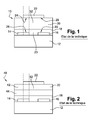
- FIG. 1 there is shown an organic thin film transistor 10 according to the state of the art having a structure "high gate - low contact”.
- the transistor 10 comprises a substrate 12, on which are formed two conductive elements 14, 16 respectively constituting the drain and the source of the transistor 10.
- a semiconductor layer 18 is deposited on the drain 14 and the source 16, the semiconductor layer conductive 18 itself being covered by a dielectric layer 20, on which is formed a third conductive element 22 constituting the gate of transistor 10.
- the transistor effect is obtained by applying a voltage between the gate 22 and the substrate 12 so as to create, in the semiconductor layer 18, a carrier channel 23 between the drain 14 and the source 16.
- the grid 22 partially covers these.
- the grid 22 has a surface 24 facing a surface 26 of the drain 14 and a surface 28 opposite a surface 30 of the source 16.
- the dielectric layer 20 may consist of a dielectric of low relative electrical permittivity, or dielectric "low k”, characterized by relative permittivity values less than 4.
- the decrease in the permittivity of the dielectric layer 20 is accompanied by an increase in the supply voltage between the gate 22 and the substrate 12 to create the carrier channel between the drain 14 and the source 16.
- Another solution is to reduce the thickness of the dielectric layer 20 to reduce stray capacitances.
- the decrease in the thickness of this layer is accompanied in particular by an increase in the leakage currents and the electrical instability of the transistor.
- the capacitance of the region 32 of the dielectric layer 20 arranged above the channel 23 is also modified.
- this capacitance must be high, in particular to avoid hysteresis phenomena that affect the quality of the transistor 10.
- This transistor 44 shown in FIG. figure 2 , is similar to that described in relation to the figure 1 , with the difference that the dielectric layer 20 comprises a first underlayer 42 of dielectric with a high relative dielectric permittivity, or "high k" material, on the grid side, and a second underlayer 44 of "low k” dielectric, source side and drain.
- a "high k” dielectric is characterized by a relative dielectric permittivity greater than or equal to 4, certain "high k” materials having a relative dielectric permittivity of up to 100, or even beyond.
- the object of the present invention is to solve the aforementioned problems by proposing an organic thin film transistor, which allows a high capacitance above the channel, a supply voltage and reduced parasitic capacitances.
- the dielectric portion between the surfaces opposite the gate and the source and the dielectric portion between the facing surfaces of the gate and the drain consist essentially of dielectric of low value of relative dielectric permittivity , effectively reducing parasitic capacitances.
- the dielectric portion between the gate and the carrier channel forming between the drain and the source essentially sees dielectric having a high value of relative dielectric permittivity.
- the capacitance of this portion of dielectric is high, which reduces the hysteresis phenomena and makes it possible to reduce the voltage between the gate and the substrate necessary for the formation of the carrier channel in the semiconductor layer.
- the generally decreasing section of the volume of the second material creates a dielectric permittivity gradient in the dielectric layer.
- This dielectric permittivity gradient makes it possible to increase the performance of the transistor.
- the relative dielectric permittivity of the first material is less than or equal to two, and the relative dielectric permittivity of the second material is greater than or equal to eight.
- the volume has a decreasing section in a monotonous manner. More particularly, the volume is a volume of revolution, in particular conical, or trapezoidal.
- the dielectric permittivity gradient decreases monotonically as a function of the thickness of the dielectric layer, which concentrates the electric field lines to the carrier channel formed between the drain and the source.
- the dielectric layer comprises a portion of the first dielectric material above the space between the drain and the source.
- a portion of the first dielectric material is present above the surface of the semiconductor layer, which reduces the electrical instabilities in the transistor.
- the thickness of the portion of the first dielectric material is less than 400 nanometers thus making it possible to obtain a high capacitance above the carrier channel, while avoiding problems of leakage current and breakdown.
- the second material is metallic. More particularly, the grid is metallic, and the volume of the second material is formed integrally therewith.
- the second material is a dielectric.
- the dielectric is preferably Al 2 O 3 alumina.
- the second material comprises nanocharges with relative dielectric permittivity greater than four dispersed in an organic matrix with relative dielectric permittivity of less than four.
- the nanofillers which generally have a diameter of between about 30 nanometers and about 50 nanometers, preferably have a relative dielectric permittivity greater than 100, and are nanoparticles included in the group consisting of BaTiO 3 , Ta 2 O 5 , Al 2 O 3 and TiO 2 . These nanoparticles have the advantage of having a very high relative dielectric permittivity and their nanoscale dimensions make it possible to disperse them homogeneously in a material with a low relative dielectric permittivity.
- the first dielectric material is fluoropolymer or polystyrene.
- this method is specially adapted for the manufacture of the dielectric layer used in the constitution of the transistor according to the invention.
- this method is specially adapted for the manufacture of the dielectric layer used in the constitution of the transistor according to the invention.
- an organic thin film transistor according to a first embodiment of the invention having the structure "high gate - low contact”, is illustrated schematically under the general reference 50.
- the transistor 50 comprises a substrate 52 on which are formed two conductive elements 54, 56 respectively constituting the drain and the source of the transistor 50.
- a semiconductor layer 58 is deposited on the drain 54 and the source 56, the semiconductor layer conductive 58 being itself covered by a dielectric layer 60 on which is formed a third conductive element 62 constituting the gate of transistor 50.
- the dielectric layer 60 comprises a layer 64 of "low k” dielectric, in particular a "low k” polymer such as a fluoropolymer or polystyrene, in which a cavity 66 filled with a "high k” dielectric is formed. .
- the cavity 66 formed in the "low k" dielectric layer 64 which starts under the grid 22 with a large surface 70, has a decreasing section as a function of the thickness of the layer 64, the minimum section 72 of the cavity 66 facing the semiconductor portion 63 between the drain 54 and the source 56 in which the carrier channel is formed.
- the cavity 66 which is preferably a volume of revolution such as a cone, terminates at a height h of the semiconductor layer 58.
- the "high k" dielectric is Al 2 O 3 alumina.
- the "high k" dielectric 68 filling the cavity 66 advantageously comprises “high k” nanocharges, with a diameter of between about 30 nanometers and about 50 nanometers and a relative dielectric permittivity preferably greater than 100, dispersed in an organic matrix, such as the "low k" polymer of the layer 64 for example, with a density greater than or equal to 6.08 g / ml.
- nanofillers are nanoparticles of BaTiO 3 , Ta 2 O 5 , Al 2 O 3 or TiO 2 .
- the transistor 80 according to this embodiment is similar to that described in connection with the figure 3 , with the difference that the cavity 66, formed in the "low k" dielectric layer 64, is filled with metal 82, and preferably of the same metal as that which constitutes the gate 22 when it is metallic. In such a case, the gate and the volume of metal filling the cavity 66 are made in one piece, which increases the mechanical strength of the transistor and simplifies the manufacturing process thereof. It will be noted that the relative dielectric permittivity of a metal is greater than the relative dielectric permittivity of the "low k" dielectric of the layer 64.
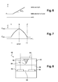
- FIG. figure 6 shows on the abscissa the equivalent dielectric relative permittivity of the layer 60 and the ordinate, the thickness thereof.
- the section of the cavity 66 decreases monotonously.
- the surface of the material of the cavity 66 in the elementary slices also decreases.
- the equivalent dielectric relative permittivity of the dielectric layer 60 therefore decreases as one approaches the semiconductor layer 58, to be equal to the relative dielectric permittivity ⁇ r 1 of the dielectric "low k" at the interface with the semiconductor layer 58.
- Such a relative dielectric permittivity gradient has the effect of improving the communication between the electric field formed in the dielectric layer 60 and the gate 62, while increasing the equivalent capacity of the portion of the dielectric layer arranged above the channel of the dielectric layer. carriers.
- the geometry of the dielectric layer 60 also makes it possible to have a maximum thickness of "low k" dielectric at the level of the drain 54 and the source 56, in order to minimize the parasitic capacitances present at the overlapping surfaces between a part of the gate 62 and the drain 64, and secondly the gate 62 and the source 56.
- the dielectric permittivity gradient in the dielectric layer 60 has the effect of increasing the transistor performance by concentrating the electric field lines towards the carrier channel formed between the drain 54 and the source 56.
- the figure 7 illustrates the evolution of the equivalent capacity of the dielectric layer 60 as a function of the width L thereof. Due to the presence of the cavity 66 filled with dielectric permittivity material greater than that of the "low k" dielectric, an advantageous capacitance profile is obtained. According to this profile, the equivalent capacity of the dielectric layer 60 is maximum at the axis of symmetry X of the cavity, that is to say above the portion 63 in which the carrier channel is formed, and decreases as one moves away from this axis, to be minimal at the level of the drain 54 and the source 56.
- the height h of dielectric "low k" present in the cavity 66 completely covers the semiconductor layer 58, which reduces the dielectric instabilities in the transistor.
- the value of the equivalent capacitance of the dielectric layer 60 at the level of the carrier channel depends mainly on the "low k" dielectric height covering the semiconductor layer 58, and more particularly depends inversely on this height h .
- a height h less than 400 nanometers makes it possible in particular to reach a high capacitance between the gate 62 and the carrier channel.
- a dielectric "low k" of relative dielectric permittivity equal to 2 2
- we obtain a capacity of about 4 nanofarads per cm 2 As this capacity evolves little for values of height h greater than 400 nanometers, by choosing a height h less than 400 nanometers, one thus has a high capacity while avoiding electrical problems such as currents of leakage or breakdowns.
- a "high k" dielectric and a metal each define a relative dielectric permittivity gradient and a variable capacitance when they form a decreasing volume in a "low k” dielectric layer
- a larger relative dielectric permittivity gradient is obtained with the dielectric "high k” only with metal.
- a larger capacity variation is obtained using a metal than with a "high k” dielectric.
- the choice of materials used to fill the cavity 66 therefore depends on the intended application. For example if the material "low k" is of low quality, the material filling the cavity 66 is preferably a dielectric "high k", such as a ceramic "high k” for example. Conversely, if the material "low k” is of good quality, the material filling the cavity 66 may have a relative dielectric permittivity not very high, and may be metal.
- a volume the section of which decreases monotonically as a function of the thickness of the dielectric layer "low k"
- a permittivity gradient and a variable capacitance are obtained. that is the shape of the volume when it has a surface at the interface with the grid larger than the surface facing the region of the semiconductor layer 58 in which is formed the carrier channel.
- the volume may be trapezoidal or pyramidal.
- the choice of the type of section of the cavity 66 (circular, square, etc.) can be dictated by the shape of the grid 62 if it is decided that the cavity 66 exactly covers the grid 62.
- the dielectric layer 60 comprises portions of high-k dielectric or metal between the surfaces opposite the gate 62 and the drain 54 and the source 56.
- the cavity 66 is formed only in the portion of the dielectric "low k" above the portion 63 of the semiconductor layer 58 in which the carrier channel is formed. The parasitic capacitances are thus further reduced.
- transistors having a so-called “high gate-bottom contact” structure (more commonly known as “ top gate-bottom contact” ).
- the present invention also applies to transistor structures called “low-contact grid down” (or “bottom gate - bottom telling"), “high grid - touch up” (or “top gate - top contact”) and “low gate - high contact” (or “bottom gate - top contact “).
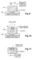
- FIGS 9 to 11 illustrate a first method of manufacturing a "low k" dielectric layer in which a decreasing section volume of "high k” dielectric, as implemented in a transistor according to the invention, is provided.
- a drop 100 of a mixture of "high k" dielectric nanoparticles, such as nanoparticles of BaTiO 3 , Ta 2 O 5 , Al 2 O 3 or TiO 2 , and of solvent is deposited, for example by a an ink jet technique, on the surface of a "low k" dielectric layer 102, and more particularly a "low k” polymer such as a fluoropolymer such as polystyrene with a relative dielectric permittivity of between 2 and 2, 5.
- the "low k" polymer layer 102 is then heated, for example by means of a heating plate 104 on which it rests, at a temperature sufficient to effectively evaporate the solvent from the deposited droplet 100, for example the temperature of the evaporation of the solvent.
- a heating temperature for example, using toluene as a solvent, a heating temperature of about 100 ° C is selected.
- the drop 100 thus dissolves partially in the polymer 102 by forming a decreasing section volume of "high k" nanofillers dispersed in an organic matrix (here the polymer "low k”), such as a cone or a truncated cone ( figure 11 ).
- a layer of a first "low k" dielectric material is etched, for example by etching, laser abrasion, embossing or the like. , to form therein a cavity having a generally decreasing section as a cone for example.
- the cavity thus formed is then filled with a second material having a relative dielectric permittivity greater than that of the first material, such as a "high k" dielectric or a metal, the filling being for example made by means of a dispersion of a liquid or by means of a spray deposition after masking the zones of the layer of the first material not to be modified.
- a second material having a relative dielectric permittivity greater than that of the first material such as a "high k" dielectric or a metal
Abstract
Description
La présente invention a trait au domaine des transistors organiques, comme par exemple les transistors à film mince plus communément connus sous l'expression anglo-saxonne « OTFT » (pour « Organic thin film transistor »).The present invention relates to the field of organic transistors, such as for example the thin film transistors more commonly known by the English expression "OTFT" (for " Organic thin film transistor" ).
Sur la
Le transistor 10 comporte un substrat 12, sur lequel sont formés deux éléments conducteurs 14, 16 constituant respectivement le drain et la source du transistor 10. Une couche semi-conductrice 18 est déposée sur le drain 14 et la source 16, la couche semi-conductrice 18 étant elle-même recouverte par une couche de diélectrique 20, sur laquelle est formé un troisième élément conducteur 22, constituant la grille du transistor 10. The
Comme cela est connu en soi, l'effet transistor est obtenu en appliquant une tension entre la grille 22 et le substrat 12 de manière à créer, dans la couche semi-conductrice 18, un canal de porteurs 23 entre le drain 14 et la source 16. Pour obtenir un canal 23 qui s'étende avec certitude du drain 14 à la source 16, la grille 22 recouvre partiellement ceux-ci. Ainsi, la grille 22 présente une surface 24 en regard d'une surface 26 du drain 14 et une surface 28 en regard d'une surface 30 de la source 16. As is known per se, the transistor effect is obtained by applying a voltage between the
Toutefois, deux conducteurs ayant des surfaces en regard et séparés par une couche diélectrique forment une capacité. On observe ainsi que des capacités parasites existent d'une part entre la grille 22 et le drain 14, et d'autre part entre la grille 22 et la source 16 en raison des surfaces en regard 24 et 26 et des surfaces en regard 28 et 30. However, two conductors having facing surfaces and separated by a dielectric layer form a capacitance. It is thus observed that parasitic capacitors exist on the one hand between the
Pour diminuer de telles capacités parasites, la couche diélectrique 20 peut être constituée d'un diélectrique de faible permittivité électrique relative, ou diélectrique « low k », caractérisé par des valeurs de permittivité relative inférieure à 4.To reduce such parasitic capacitances, the
Or, plus un matériau présente une permittivité électrique relative faible, plus il est difficilement polarisable. De fait, la diminution de la permittivité de la couche diélectrique 20 s'accompagne d'une augmentation de la tension d'alimentation entre la grille 22 et le substrat 12 pour créer le canal de porteurs entre le drain 14 et la source 16. However, the more a material has a low relative electrical permittivity, the more it is difficult to polarize. In fact, the decrease in the permittivity of the
Augmenter la tension d'alimentation pose cependant des problèmes de coût et nécessite des transistors de plus grandes surfaces qui puissent supporter des tensions plus élevées. La réalisation de transistors organiques de grande surface nécessite usuellement la mise en oeuvre de techniques de fabrication par voie liquide ou d'impression. Or, ce type de techniques est généralement efficace avec des semi-conducteurs de type P, mais s'avère de mise en oeuvre difficile pour des conducteurs de type N, ce qui réduit d'emblée le type de transistors réalisables.Increasing the supply voltage, however, causes cost problems and requires larger-area transistors that can withstand higher voltages. The production of large-area organic transistors usually requires the implementation of manufacturing techniques by liquid or printing. However, this type of technique is generally effective with P-type semiconductors, but is difficult to implement for N-type conductors, which immediately reduces the type of transistors feasible.
Une autre solution consiste à diminuer l'épaisseur de la couche de diélectrique 20 afin de réduire les capacités parasites. Cependant la diminution de l'épaisseur de cette couche s'accompagne notamment d'une augmentation des courants de fuite et de l'instabilité électrique du transistor.Another solution is to reduce the thickness of the
En outre, en modifiant les propriétés globales de la couche diélectrique 20, notamment pour diminuer les capacités parasites, on modifie également la capacité de la région 32 de la couche diélectrique 20 agencée au dessus du canal 23. Or, cette capacité doit être élevée, notamment pour éviter des phénomènes d'hystérésis qui nuisent à la qualité du transistor 10. In addition, by modifying the overall properties of the
Pour pallier certains de ces inconvénients, il a été proposé, un transistor dont la permittivité diélectrique relative de la couche semi-conductrice varie en fonction de son épaisseur. Ce transistor 44, illustré à la
Comme cela est connu en soi, un diélectrique « high k » est caractérisé par une permittivité diélectrique relative supérieure ou égale à 4, certains matériaux « high k » ayant une permittivité diélectrique relative pouvant aller jusqu'à 100, voire même au-delà.As is known per se, a "high k" dielectric is characterized by a relative dielectric permittivity greater than or equal to 4, certain "high k" materials having a relative dielectric permittivity of up to 100, or even beyond.
Un tel agencement permet de diminuer la tension d'alimentation du diélectrique et d'augmenter la capacité dans la région 32 mais ne règle pas de façon efficace le problème des capacités de fuite qui sont toujours présentes.Such an arrangement makes it possible to reduce the supply voltage of the dielectric and to increase the capacitance in the
Le but de la présente invention est de résoudre les problèmes susmentionnés en proposant un transistor organique à film mince, qui permette une capacité élevée au dessus du canal, une tension d'alimentation et des capacités parasites réduites.The object of the present invention is to solve the aforementioned problems by proposing an organic thin film transistor, which allows a high capacitance above the channel, a supply voltage and reduced parasitic capacitances.
A cet effet, l'invention a pour objet un transistor organique à film mince comportant :
- ■ un élément conducteur formant drain ;
- ■ un élément conducteur formant source espacé du drain ;
- ■ un élément conducteur formant grille présentant une surface en regard du drain et une surface en regard de la source ;
- ■ une couche semi-conductrice au contact du drain et de la source ; et
- ■ une couche diélectrique agencée entre d'une part la grille et d'autre part la source et le drain, la couche diélectrique présentant une permittivité diélectrique variable en fonction de son épaisseur,
- A conductive element forming a drain;
- A conductive element forming a source spaced from the drain;
- A conductive element forming a grid having a surface facing the drain and a surface facing the source;
- A semiconductor layer in contact with the drain and the source; and
- A dielectric layer arranged between, on the one hand, the gate and on the other hand the source and the drain, the dielectric layer having a variable dielectric permittivity as a function of its thickness,
Selon l'invention :
- la couche diélectrique comporte une couche d'un premier matériau diélectrique de permittivité diélectrique relative inférieure à quatre dans laquelle est formé, au moins entre lesdites surfaces en regard, un volume d'un second matériau, ledit volume ayant une section globalement décroissante depuis la grille vers l'espace entre le drain et la source,
- et la permittivité diélectrique relative du second matériau est supérieure à quatre.
- the dielectric layer comprises a layer of a first dielectric material with a relative dielectric permittivity of less than four, in which a volume of a second material is formed, at least between said facing surfaces, said volume having a generally decreasing cross section from the grid to the space between the drain and the source,
- and the relative dielectric permittivity of the second material is greater than four.
Il est entendu que dans le présent document une permittivité diélectrique relative est dite faible lorsqu'elle est inférieure à 4 et élevée lorsqu'elle est supérieure à 4.It is understood that in this document a relative dielectric permittivity is said to be low when it is less than 4 and high when it is greater than 4.
Par « globalement », on entend ici que la section du volume proche de la grille est supérieure à la section du volume proche de la région de la couche semi-conductrice entre le drain et la source dans laquelle se forme le canal de porteurs, la section du volume pouvant décroitre de manière monotone ou non.By "globally" is meant here that the section of the volume close to the gate is greater than the section of the volume near the region of the semiconductor layer between the drain and the source in which the carrier channel is formed, the section of volume that can decrease monotonously or not.
En d'autres termes, la portion de diélectrique entre les surfaces en regard de la grille et de la source et la portion de diélectrique entre les surfaces en regard de la grille et du drain sont essentiellement constituées de diélectrique de faible valeur de permittivité diélectrique relative, réduisant de fait les capacités parasites. En outre, la portion de diélectrique entre la grille et le canal de porteurs se formant entre le drain et la source voit essentiellement du diélectrique ayant une valeur élevée de permittivité diélectrique relative. De fait, la capacité de cette portion de diélectrique est élevée, ce qui réduit les phénomènes d'hystérésis et permet de diminuer la tension entre la grille et le substrat nécessaire à la formation du canal de porteurs dans la couche semi-conductrice.In other words, the dielectric portion between the surfaces opposite the gate and the source and the dielectric portion between the facing surfaces of the gate and the drain consist essentially of dielectric of low value of relative dielectric permittivity , effectively reducing parasitic capacitances. In addition, the dielectric portion between the gate and the carrier channel forming between the drain and the source essentially sees dielectric having a high value of relative dielectric permittivity. In fact, the capacitance of this portion of dielectric is high, which reduces the hysteresis phenomena and makes it possible to reduce the voltage between the gate and the substrate necessary for the formation of the carrier channel in the semiconductor layer.
Par ailleurs, la section globalement décroissante du volume du second matériau crée dans la couche diélectrique un gradient de permittivité diélectrique. Ce gradient de permittivité diélectrique permet d'augmenter les performances du transistor.On the other hand, the generally decreasing section of the volume of the second material creates a dielectric permittivity gradient in the dielectric layer. This dielectric permittivity gradient makes it possible to increase the performance of the transistor.
On notera à cet égard que prévoir un volume de section constante au dessus de la région semi-conductrice dans laquelle se forme le canal de porteurs, comme un cylindre de matériau « high k » par exemple, ne permet pas d'obtenir un transistor fonctionnant de manière satisfaisante en raison de l'absence d'un tel gradient de permittivité relative.It will be noted in this respect that providing a volume of constant section above the semiconductor region in which the carrier channel is formed, such as a cylinder of material "high k" for example, does not make it possible to obtain a transistor operating satisfactorily because of the absence of such a relative permittivity gradient.
De préférence, la permittivité diélectrique relative du premier matériau est inférieur ou égale à deux, et la permittivité diélectrique relative du second matériau est supérieure ou égale à huit.Preferably, the relative dielectric permittivity of the first material is less than or equal to two, and the relative dielectric permittivity of the second material is greater than or equal to eight.
Selon un mode de réalisation particulier de l'invention, le volume présente une section décroissante de manière monotone. Plus particulièrement, le volume est un volume de révolution, notamment conique, ou trapézoïdal.According to a particular embodiment of the invention, the volume has a decreasing section in a monotonous manner. More particularly, the volume is a volume of revolution, in particular conical, or trapezoidal.
En d'autres termes, le gradient de permittivité diélectrique décroit de manière monotone en fonction de l'épaisseur de la couche de diélectrique, ce qui concentre les lignes de champs électriques vers le canal de porteurs formé entre le drain et la source.In other words, the dielectric permittivity gradient decreases monotonically as a function of the thickness of the dielectric layer, which concentrates the electric field lines to the carrier channel formed between the drain and the source.
Selon un mode de réalisation particulier de l'invention, la couche diélectrique comporte une portion du premier matériau diélectrique au dessus de l'espace entre le drain et la source.According to a particular embodiment of the invention, the dielectric layer comprises a portion of the first dielectric material above the space between the drain and the source.
En d'autres termes, une portion du premier matériau diélectrique est présente au dessus de la surface de la couche semi-conductrice, ce qui réduit les instabilités électriques dans le transistor.In other words, a portion of the first dielectric material is present above the surface of the semiconductor layer, which reduces the electrical instabilities in the transistor.
Plus particulièrement, l'épaisseur de la portion du premier matériau diélectrique est inférieure à 400 nanomètres permettant ainsi d'obtenir une capacité élevée au dessus du canal de porteurs, tout en évitant les problèmes de courant de fuite et de claquage.More particularly, the thickness of the portion of the first dielectric material is less than 400 nanometers thus making it possible to obtain a high capacitance above the carrier channel, while avoiding problems of leakage current and breakdown.
Selon un mode de réalisation particulier de l'invention, le second matériau est métallique. Plus particulièrement, la grille est métallique, et le volume du second matériau est formé d'un seul tenant avec celle-ci.According to a particular embodiment of the invention, the second material is metallic. More particularly, the grid is metallic, and the volume of the second material is formed integrally therewith.
Selon une mode de réalisation particulier de l'invention, le second matériau est un diélectrique. Dans une première variante, le diélectrique est préférentiellement de l'alumine Al2O3. Dans une seconde variante, le second matériau comporte des nanocharges à permittivité diélectrique relative supérieure à quatre dispersées dans une matrice organique à permittivité diélectrique relative inférieure à quatre. Les nanocharges, qui ont en général un diamètre compris entre environ 30 nanomètres et environ 50 nanomètres, ont de préférence une permittivité diélectrique relative supérieure à 100, et sont des nanoparticules comprises dans le groupe constitué de BaTiO3, Ta2O5, Al2O3 et TiO2. Ces nanoparticules présentent l'avantage d'avoir une très forte permittivité diélectrique relative et leurs dimensions nanométriques permettent de les disperser de façon homogène dans un matériau à faible permittivité diélectrique relative.According to a particular embodiment of the invention, the second material is a dielectric. In a first variant, the dielectric is preferably Al 2 O 3 alumina. In a second variant, the second material comprises nanocharges with relative dielectric permittivity greater than four dispersed in an organic matrix with relative dielectric permittivity of less than four. The nanofillers, which generally have a diameter of between about 30 nanometers and about 50 nanometers, preferably have a relative dielectric permittivity greater than 100, and are nanoparticles included in the group consisting of BaTiO 3 , Ta 2 O 5 , Al 2 O 3 and TiO 2 . These nanoparticles have the advantage of having a very high relative dielectric permittivity and their nanoscale dimensions make it possible to disperse them homogeneously in a material with a low relative dielectric permittivity.
Selon un mode de réalisation particulier de l'invention, le premier matériau diélectrique est du fluoropolymère ou du polystyrène.According to a particular embodiment of the invention, the first dielectric material is fluoropolymer or polystyrene.
L'invention a également pour objet un procédé de fabrication d'une couche de diélectrique pour transistor organique présentant un gradient de permittivité diélectrique en fonction de son épaisseur, ledit procédé comportant :
- ■ une étape de formation d'une couche d'un premier matériau diélectrique ;
- ■ une étape de dépôt, sur la surface de la couche du premier matériau, d'un mélange de solvant et de nanocharges présentant une permittivité diélectrique relative supérieure à celle du premier matériau ; et
- ■ une étape de chauffage de la couche du premier matériau diélectrique, la compétition entre l'évaporation du solvant par chauffage et la pénétration par absorption des nanocharges par le premier matériau diélectrique formant dans la couche du premier matériau un volume d'un second matériau de section globalement décroissante en fonction de l'épaisseur de la couche du premier matériau et de permittivité diélectrique relative supérieure à celle du premier matériau.
- A step of forming a layer of a first dielectric material;
- A deposition step, on the surface of the layer of the first material, of a mixture of solvent and nanofillers having a relative dielectric permittivity greater than that of the first material; and
- A step of heating the layer of the first dielectric material, the competition between the evaporation of the solvent by heating and the absorption penetration of the nanofillers by the first dielectric material forming in the layer of the first material a volume of a second material of section decreasing overall depending on the thickness of the first material layer and relative dielectric permittivity greater than that of the first material.
En d'autres termes, ce procédé est spécialement adapté pour la fabrication de la couche diélectrique entrant dans la constitution du transistor selon l'invention.In other words, this method is specially adapted for the manufacture of the dielectric layer used in the constitution of the transistor according to the invention.
L'invention a également pour objet un procédé de fabrication d'une couche de diélectrique pour transistor organique présentant un gradient de permittivité diélectrique en fonction de son épaisseur, ledit procédé comportant :
- ■ une étape de formation d'une couche d'un premier matériau diélectrique
- ■ une étape de gravure dans le premier matériau diélectrique d'une cavité ayant section globalement décroissante ; et
- ■ une étape de remplissage de ladite cavité par un second matériau présentant une permittivité diélectrique relative supérieure à celle du premier matériau.
- A step of forming a layer of a first dielectric material
- A step of etching in the first dielectric material of a cavity having a generally decreasing cross section; and
- A step of filling said cavity with a second material having a relative dielectric permittivity greater than that of the first material.
En d'autres termes, ce procédé est spécialement adapté pour la fabrication de la couche diélectrique entrant dans la constitution du transistor selon l'invention.In other words, this method is specially adapted for the manufacture of the dielectric layer used in the constitution of the transistor according to the invention.
La présente invention sera mieux comprise à la lecture de la description qui suit, réalisée en relation avec les dessins annexés, dans lesquels des références identiques désignent des éléments identiques ou analogues, et dans lesquels :
- la
figure 1 est une vue schématique en section d'un premier transistor organique à film mince de l'état de la technique décrit dans le préambule ; - la
figure 2 est une vue schématique en section d'un second transistor organique à film mince de l'état de la technique décrit dans le préambule ; - la
figure 3 est une vue schématique en section d'un transistor organique à film mince selon une premier mode de réalisation de l'invention ; - la
figure 4 est une vue schématique en section d'un transistor organique à film mince selon une deuxième mode de réalisation de l'invention ; - la
figure 5 est une vue schématique de la couche diélectrique des transistors desfigures 3 et 4 sur laquelle sont représentées des tranches élémentaires de celle-ci ; - la
figure 6 est une courbe illustrant l'évolution de la permittivité diélectrique relative de la couche semi-conductrice entrant dans la constitution des transistors desfigures 3 et 4 en fonction de l'épaisseur de celle-ci ; - la
figure 7 est une courbe illustrant l'évolution de la capacité de la couche semi-conductrice entrant dans la constitution des transistors desfigures 3 et 4 en fonction de la largeur de celle-ci ; - la
figure 8 est une vue schématique en section d'un transistor organique à film mince selon une troisième mode de réalisation de l'invention ; - les
figures 9 à 11 sont des vues schématiques illustrant un procédé de fabrication selon l'invention de la couche semi-conductrice entrant dans la constitution du transistor de lafigure 4 .
- the
figure 1 is a schematic sectional view of a first organic thin film transistor of the state of the art described in the preamble; - the
figure 2 is a schematic sectional view of a second organic thin film transistor of the state of the art described in the preamble; - the
figure 3 is a schematic sectional view of an organic thin film transistor according to a first embodiment of the invention; - the
figure 4 is a schematic sectional view of an organic thin film transistor according to a second embodiment of the invention; - the
figure 5 is a schematic view of the dielectric layer of the transistors ofFigures 3 and 4 on which are represented elementary slices of it; - the
figure 6 is a curve illustrating the evolution of the relative dielectric permittivity of the semiconductor layer forming part of the transistors of theFigures 3 and 4 depending on the thickness of it; - the
figure 7 is a curve illustrating the evolution of the capacity of the semiconductor layer entering the constitution of the transistors of theFigures 3 and 4 depending on the width of the latter; - the
figure 8 is a diagrammatic sectional view of an organic thin film transistor according to a third embodiment of the invention; - the
Figures 9 to 11 are schematic views illustrating a manufacturing method according to the invention of the semiconductor layer forming part of the transistor of thefigure 4 .
Sur la
Le transistor 50 comporte un substrat 52 sur lequel sont formés deux éléments conducteurs 54, 56, constituant respectivement le drain et la source du transistor 50. Une couche semi-conductrice 58 est déposée sur le drain 54 et la source 56, la couche semi-conductrice 58 étant elle-même recouverte par une couche de diélectrique 60 sur laquelle est formé un troisième élément conducteur 62, constituant la grille du transistor 50. The
Selon l'invention, la couche diélectrique 60 comporte une couche 64 de diélectrique « low k », notamment un polymère « low k » comme un fluoropolymère ou un polystyrène, dans laquelle est formée une cavité 66 remplie d'un diélectrique « high k ».According to the invention, the
La cavité 66 formée dans la couche de diélectrique « low k » 64, qui débute sous la grille 22 avec une grande surface 70, présente une section décroissante en fonction de l'épaisseur de la couche 64, la section minimale 72 de la cavité 66 faisant face à la portion 63 de semi-conducteur entre le drain 54 et la source 56 dans laquelle se forme le canal de porteurs. La cavité 66, qui est de préférence un volume de révolution tel qu'un cône, se termine à une hauteur h de la couche de semi-conducteur 58. The
Dans une première variante, le diélectrique « high k » est de l'alumine Al2O3.In a first variant, the "high k" dielectric is Al 2 O 3 alumina.
Dans une seconde variante, le diélectrique « high k » 68 remplissant la cavité 66, comporte avantageusement des nanocharges « high k », de diamètre compris entre environ 30 nanomètres et environ 50 nanomètres et de permittivité diélectrique relative de préférence supérieure à 100, dispersées dans une matrice organique, telle que le polymère « low k » de la couche 64 par exemple, avec une densité supérieure ou égale à 6.08 g/ml. Par exemple, les nanocharges sont des nanoparticules de BaTiO3, de Ta2O5, de Al2O3 ou de TiO2.In a second variant, the "high k" dielectric 68 filling the
Sur la
Grâce à la formation de la cavité 66 remplie de diélectrique « high k » ou de métal dans la couche de diélectrique « low k » 64, il est ainsi obtenu un gradient de permittivité diélectrique relative dans l'épaisseur de la couche 64. Due to the formation of
En effet, comme cela est visible sur la ![]()
- S 1(dxi ) est la surface de la portion de tranche élémentaire « dxi » correspondant au diélectrique « low k » de permittivité diélectrique relative ε r1,
- et S 2(dxi ) est la surface de la portion de tranche élémentaire « dxi » correspondant au matériau remplissant la cavité 66 (diélectrique « high k » 68 ou métal 82) de permittivité diélectrique relative ε r2.
- S 1 ( dx i ) is the area of the elementary slice portion " dx i " corresponding to the "low k" dielectric of relative dielectric permittivity ε r 1 ,
- and S 2 ( dx i ) is the surface of the elementary wafer portion " dx i " corresponding to the material filling the cavity 66 (
high k dielectric 68 or metal 82) of relative dielectric permittivity ε r 2 .
De fait, il existe en fonction de l'épaisseur e de la couche diélectrique 60, un gradient de permittivité diélectrique, comme cela est visible à la
La section de la cavité 66, ici un cône, décroit de façon monotone. La surface du matériau de la cavité 66 dans les tranches élémentaires diminue également. La permittivité diélectrique relative équivalente de la couche diélectrique 60 diminue donc à mesure qu'on se rapproche de la couche de semi-conducteur 58, pour être égale à la permittivité diélectrique relative ε r1 du diélectrique « low k » à l'interface avec la couche de semi-conducteur 58. The section of the
Un tel gradient de permittivité diélectrique relative a pour effet d'améliorer la communication entre le champ électrique formé dans la couche de diélectrique 60 et la grille 62, tout en augmentant la capacité équivalente de la portion de la couche diélectrique agencée au dessus du canal de porteurs. La géométrie de la couche de diélectrique 60 permet également d'avoir une épaisseur maximale de diélectrique « low k » au niveau du drain 54 et de la source 56, afin de minimiser les capacités parasites présentes au niveau des surfaces de recouvrement entre d'une part la grille 62 et le drain 64, et d'autre part la grille 62 et la source 56. Such a relative dielectric permittivity gradient has the effect of improving the communication between the electric field formed in the
Par ailleurs, le gradient de permittivité diélectrique dans la couche diélectrique 60 a pour effet d'augmenter les performances du transistor en concentrant les lignes de champ électrique vers le canal de porteurs formé entre le drain 54 et la source 56. Moreover, the dielectric permittivity gradient in the
La
Par ailleurs, la hauteur h de diélectrique « low k » présente sous la cavité 66 recouvre intégralement la couche semi-conductrice 58, ce qui réduit les instabilités diélectriques dans le transistor.Moreover, the height h of dielectric "low k" present in the
On observe en outre que la valeur de la capacité équivalente de la couche diélectrique 60 au niveau du canal de porteurs dépend principalement de la hauteur de diélectrique « low k » recouvrant la couche semi-conductrice 58, et plus particulièrement dépend de manière inverse de cette hauteur h. Une hauteur h inférieure à 400 nanomètres permet notamment d'atteindre une capacité élevée entre la grille 62 et le canal de porteurs. A titre d'exemple, avec un diélectrique « low k » de permittivité diélectrique relative égale à 2, on obtient une capacité d'environ 4 nanofarads par cm2. Comme cette capacité évolue peu pour des valeurs de hauteur h supérieure à 400 nanomètres, en choisissant une hauteur h inférieure à 400 nanomètres, on a donc une capacité élevée tout en évitant des problèmes électriques tels que des courants de fuite ou des claquages.It is further observed that the value of the equivalent capacitance of the
Bien qu'un diélectrique « high k » et un métal définissent chacun un gradient de permittivité diélectrique relative et une capacité variable lorsqu'ils forment un volume décroissant dans une couche de diélectrique « low k », un gradient de permittivité diélectrique relative plus important est obtenu à l'aide du diélectrique « high k » qu'avec du métal. Inversement, une variation de capacité plus importante est obtenue à l'aide d'un métal qu'avec un diélectrique « high k ». Le choix des matériaux utilisés pour remplir la cavité 66 dépend donc de l'application visée. Par exemple si le matériau « low k » est de faible qualité, le matériau remplissant la cavité 66 est préférentiellement un diélectrique « high k », comme un céramique « high k » par exemple. A l'inverse, si le matériau « low k » est de bonne qualité, le matériau remplissant la cavité 66 peut présenter une permittivité diélectrique relative pas très élevée, et peut être du métal.Although a "high k" dielectric and a metal each define a relative dielectric permittivity gradient and a variable capacitance when they form a decreasing volume in a "low k" dielectric layer, a larger relative dielectric permittivity gradient is obtained with the dielectric "high k" only with metal. Conversely, a larger capacity variation is obtained using a metal than with a "high k" dielectric. The choice of materials used to fill the
Bien entendu, l'invention n'est pas limitée aux exemples décrits ci-dessus.Of course, the invention is not limited to the examples described above.
Bien qu'un volume, dont la section décroît de manière monotone en fonction de l'épaisseur de la couche de diélectrique « low k », soit préféré pour éviter les capacités parasites de recouvrement, un gradient de permittivité et une capacité variable sont obtenus quelle que soit la forme du volume dès lors que celui-ci présente une surface à l'interface avec la grille plus grande que la surface en regard de la région de la couche semi-conductrice 58 dans laquelle est formé le canal de porteurs. Par exemple, le volume peut être trapézoïdal ou pyramidal. Notamment, le choix du type de section de la cavité 66 (circulaire, carrée, etc...) peut être dicté par la forme de la grille 62 s'il est décidé que la cavité 66 recouvre exactement la grille 62. Although a volume, the section of which decreases monotonically as a function of the thickness of the dielectric layer "low k", is preferred to avoid parasitic capacitances, a permittivity gradient and a variable capacitance are obtained. that is the shape of the volume when it has a surface at the interface with the grid larger than the surface facing the region of the
De même, il a été décrit en relation avec les
En variante, tel que cela est illustré à la
De même, il a été décrit des transistors présentant une structure dite « grille haute - contact bas » (plus communément connue sous l'expression anglo-saxonne « top gate-bottom contact »). Bien entendu, la présente invention s'applique également aux structures de transistors dites « grille basse-contact bas » (ou « bottom gate - bottom contant »), « grille haute - contact haut » (ou « top gate - top contact ») et « grille basse - contact haut » (ou « bottom gate - top contact »).Similarly, there have been described transistors having a so-called "high gate-bottom contact" structure (more commonly known as " top gate-bottom contact" ). Of course, the present invention also applies to transistor structures called "low-contact grid down" (or "bottom gate - bottom telling"), "high grid - touch up" (or "top gate - top contact") and "low gate - high contact" (or "bottom gate - top contact ").
Les
Dans une première étape illustrée à la
Comme illustré à la
Un phénomène de compétition entre l'évaporation du la goutte 100 et la pénétration de celle-ci dans le polymère 102 est alors observé. La goutte 100 se dissout ainsi partiellement dans le polymère 102 en formant un volume de section décroissante de nanocharges « high k » dispersées dans une matrice organique (ici le polymère « low k »), tel un cône ou un cône tronqué (
Le choix du solvant ainsi que celui de la température permet notamment de régler la profondeur de pénétration des nanoparticules dans le polymère, et donc la forme finale du volume de diélectrique « high k » dans la couche de diélectrique « low k ».The choice of the solvent as well as that of the temperature makes it possible in particular to adjust the penetration depth of the nanoparticles in the polymer, and thus the final shape of the "high k" dielectric volume in the "low k" dielectric layer.
Selon un second procédé de fabrication d'une couche de diélectrique pour transistor organique selon l'invention, une couche d'un premier matériau diélectrique « low k » est gravée, par exemple par une attaque chimique, une abrasion laser, un emboutissage ou autres, pour former dans celle-ci une cavité ayant une section globalement décroissante comme un cône par exemple.According to a second method for manufacturing an organic transistor dielectric layer according to the invention, a layer of a first "low k" dielectric material is etched, for example by etching, laser abrasion, embossing or the like. , to form therein a cavity having a generally decreasing section as a cone for example.
La cavité ainsi formée est alors remplie d'un second matériau présentant une permittivité diélectrique relative supérieure à celle du premier matériau, comme un diélectrique « high k » ou un métal, le remplissage étant par exemple réalisé au moyen d'une dispersion d'un liquide ou au moyen d'un dépôt par pulvérisation après masquage des zones de la couche du premier matériau à ne pas modifier.The cavity thus formed is then filled with a second material having a relative dielectric permittivity greater than that of the first material, such as a "high k" dielectric or a metal, the filling being for example made by means of a dispersion of a liquid or by means of a spray deposition after masking the zones of the layer of the first material not to be modified.
Claims (16)
Applications Claiming Priority (1)
| Application Number | Priority Date | Filing Date | Title |
|---|---|---|---|
| FR0855300A FR2934714B1 (en) | 2008-07-31 | 2008-07-31 | ORGANIC TRANSISTOR AND METHOD FOR MANUFACTURING DIELECTRIC LAYER OF SUCH TRANSISTOR. |
Publications (2)
| Publication Number | Publication Date |
|---|---|
| EP2149924A1 true EP2149924A1 (en) | 2010-02-03 |
| EP2149924B1 EP2149924B1 (en) | 2012-05-16 |
Family
ID=40386159
Family Applications (1)
| Application Number | Title | Priority Date | Filing Date |
|---|---|---|---|
| EP09305586A Not-in-force EP2149924B1 (en) | 2008-07-31 | 2009-06-23 | Organic transistor and method for manufacturing a dielectric layer of such a transistor |
Country Status (4)
| Country | Link |
|---|---|
| US (1) | US8748872B2 (en) |
| EP (1) | EP2149924B1 (en) |
| JP (1) | JP5460142B2 (en) |
| FR (1) | FR2934714B1 (en) |
Families Citing this family (5)
| Publication number | Priority date | Publication date | Assignee | Title |
|---|---|---|---|---|
| JP5471564B2 (en) * | 2010-02-17 | 2014-04-16 | カシオ計算機株式会社 | THIN FILM TRANSISTOR AND METHOD FOR PRODUCING THIN FILM TRANSISTOR |
| JP5659568B2 (en) * | 2010-06-11 | 2015-01-28 | 富士ゼロックス株式会社 | Field effect organic transistor |
| JP6061858B2 (en) * | 2010-10-07 | 2017-01-18 | ジョージア・テック・リサーチ・コーポレーション | Field effect transistor and manufacturing method thereof |
| GB2497328A (en) * | 2011-12-07 | 2013-06-12 | Canon Kk | Method of making a dielectric material with a varying permittivity |
| TWI627935B (en) * | 2017-01-24 | 2018-07-01 | 好喜歡妮有限公司 | Interspinous stabilizer |
Citations (3)
| Publication number | Priority date | Publication date | Assignee | Title |
|---|---|---|---|---|
| US20050285102A1 (en) * | 2004-06-24 | 2005-12-29 | Jae-Bon Koo | Organic TFT and method of fabricating the same |
| WO2007074404A2 (en) * | 2005-11-14 | 2007-07-05 | Ciba Holding Inc. | Method and apparatus for patterning a conductive layer, and a device produced thereby |
| US20070215957A1 (en) * | 2006-03-17 | 2007-09-20 | Fang-Chung Chen | Gate dielectric structure and an organic thin film transistor based thereon |
Family Cites Families (5)
| Publication number | Priority date | Publication date | Assignee | Title |
|---|---|---|---|---|
| EP2204861A1 (en) * | 2001-12-19 | 2010-07-07 | Merck Patent GmbH | Organic field effect transistor with an organic dielectric |
| JP2005340410A (en) * | 2004-05-26 | 2005-12-08 | Canon Inc | Field effect transistor and manufacturing method thereof |
| KR100659103B1 (en) * | 2005-10-24 | 2006-12-19 | 삼성에스디아이 주식회사 | Organic thin film transistor, flat panel display apparatus comprising the same, and method of manufacturing the organic thin film transistor |
| JP4686232B2 (en) * | 2005-03-30 | 2011-05-25 | セイコーエプソン株式会社 | Semiconductor device and manufacturing method of semiconductor device |
| US20070254402A1 (en) * | 2006-04-27 | 2007-11-01 | Robert Rotzoll | Structure and fabrication of self-aligned high-performance organic fets |
-
2008
- 2008-07-31 FR FR0855300A patent/FR2934714B1/en not_active Expired - Fee Related
-
2009
- 2009-06-23 EP EP09305586A patent/EP2149924B1/en not_active Not-in-force
- 2009-06-24 US US12/490,816 patent/US8748872B2/en not_active Expired - Fee Related
- 2009-06-26 JP JP2009152841A patent/JP5460142B2/en not_active Expired - Fee Related
Patent Citations (3)
| Publication number | Priority date | Publication date | Assignee | Title |
|---|---|---|---|---|
| US20050285102A1 (en) * | 2004-06-24 | 2005-12-29 | Jae-Bon Koo | Organic TFT and method of fabricating the same |
| WO2007074404A2 (en) * | 2005-11-14 | 2007-07-05 | Ciba Holding Inc. | Method and apparatus for patterning a conductive layer, and a device produced thereby |
| US20070215957A1 (en) * | 2006-03-17 | 2007-09-20 | Fang-Chung Chen | Gate dielectric structure and an organic thin film transistor based thereon |
Non-Patent Citations (2)
| Title |
|---|
| DAVID R LIDE: "CRC HANDBOOK OF CHEMISTRY AND PHYSICS", 1 January 2008, TAYLOR AND FRANCIS GROUP, LLC, XP002518007 * |
| DAVID R LIDE: "CRC HANDBOOK OF CHEMISTRY AND PHYSICS", 1 January 2008, TAYLOR AND FRANCIS GROUP, LLC, XP002518008 * |
Also Published As
| Publication number | Publication date |
|---|---|
| JP5460142B2 (en) | 2014-04-02 |
| FR2934714A1 (en) | 2010-02-05 |
| JP2010041039A (en) | 2010-02-18 |
| US8748872B2 (en) | 2014-06-10 |
| EP2149924B1 (en) | 2012-05-16 |
| FR2934714B1 (en) | 2010-12-17 |
| US20100025668A1 (en) | 2010-02-04 |
Similar Documents
| Publication | Publication Date | Title |
|---|---|---|
| EP2149924B1 (en) | Organic transistor and method for manufacturing a dielectric layer of such a transistor | |
| EP1869712B1 (en) | Structure and method for realizing a microelectronic device provided with a number of quantum wires capable of forming one or more transistor channels | |
| EP2144369B1 (en) | Bulk acoustic wave resonator | |
| FR2838238A1 (en) | Semiconductor device with enveloping gate encapsulated in an insulating medium | |
| FR3016237A1 (en) | SEMICONDUCTOR NANOWELL DEVICE PARTIALLY SURROUNDED BY A GRID | |
| FR3086456A1 (en) | METHOD FOR PRODUCING SUPERIMPOSED TRANSISTORS | |
| EP1993138A2 (en) | Device with a strained-channel transistor | |
| EP1589572B1 (en) | Process of making an integrated circuit comprising hollow trench isolation | |
| FR2860249A1 (en) | METHOD FOR MANUFACTURING PLATE-LIKE STRUCTURE, ESPECIALLY SILICON, PROCESS APPLICATION, AND PLATE-LIKE STRUCTURE, PARTICULARLY SILICON | |
| EP3127142B1 (en) | Method for manufacture of a semiconductor wafer suitable for the manufacture of an soi substrate, and soi substrate wafer thus obtained | |
| FR3052592A1 (en) | STRUCTURE FOR RADIO FREQUENCY APPLICATIONS | |
| EP1346405B1 (en) | Method for making an island of material confined between electrodes, and application to transistors | |
| EP1543535B1 (en) | Method of manufacture of electrostatically actuated low response time power commutation micro-switches | |
| FR3120622A1 (en) | Electrically controlled MEMS switch and method of making same | |
| WO2009077684A1 (en) | Method for making an electric interconnection between two conducting layers | |
| FR3089343A1 (en) | PROCESS FOR PRODUCING A FET TRANSISTOR | |
| EP3916788B1 (en) | Method for manufacturing an optoelectronic device comprising a plurality of diodes | |
| EP3680936B1 (en) | Back-illuminated image sensor | |
| EP3560001A1 (en) | Light-emitting device | |
| EP3671841B1 (en) | Method for manufacturing an optoelectronic device comprising a plurality of diodes | |
| WO2003030266A1 (en) | Transistor with an electron and a vertical channel and the production methods thereof | |
| FR2805081A1 (en) | METHOD FOR MANUFACTURING DOUBLE HETEROJUNCTION BIPOLAR TRANSISTOR ON III-V MATERIAL | |
| FR2718287A1 (en) | Method for manufacturing an insulated gate field effect transistor, in particular of reduced channel length, and corresponding transistor. | |
| WO2017182739A1 (en) | Device with segmented field plates | |
| EP2567418B1 (en) | Microelectronic device having disconnected semiconductor portions and method for producing such a device |
Legal Events
| Date | Code | Title | Description |
|---|---|---|---|
| PUAI | Public reference made under article 153(3) epc to a published international application that has entered the european phase |
Free format text: ORIGINAL CODE: 0009012 |
|
| AK | Designated contracting states |
Kind code of ref document: A1 Designated state(s): AT BE BG CH CY CZ DE DK EE ES FI FR GB GR HR HU IE IS IT LI LT LU LV MC MK MT NL NO PL PT RO SE SI SK TR |
|
| AX | Request for extension of the european patent |
Extension state: AL BA RS |
|
| RAP1 | Party data changed (applicant data changed or rights of an application transferred) |
Owner name: COMMISSARIAT A L'ENERGIE ATOMIQUE |
|
| 17P | Request for examination filed |
Effective date: 20100211 |
|
| RAP1 | Party data changed (applicant data changed or rights of an application transferred) |
Owner name: COMMISSARIAT A L'ENERGIE ATOMIQUE ET AUX ENERGIES |
|
| 17Q | First examination report despatched |
Effective date: 20100527 |
|
| RIC1 | Information provided on ipc code assigned before grant |
Ipc: H01L 51/10 20060101AFI20110912BHEP |
|
| GRAP | Despatch of communication of intention to grant a patent |
Free format text: ORIGINAL CODE: EPIDOSNIGR1 |
|
| GRAS | Grant fee paid |
Free format text: ORIGINAL CODE: EPIDOSNIGR3 |
|
| GRAA | (expected) grant |
Free format text: ORIGINAL CODE: 0009210 |
|
| AK | Designated contracting states |
Kind code of ref document: B1 Designated state(s): AT BE BG CH CY CZ DE DK EE ES FI FR GB GR HR HU IE IS IT LI LT LU LV MC MK MT NL NO PL PT RO SE SI SK TR |
|
| REG | Reference to a national code |
Ref country code: GB Ref legal event code: FG4D Free format text: NOT ENGLISH |
|
| REG | Reference to a national code |
Ref country code: CH Ref legal event code: EP |
|
| REG | Reference to a national code |
Ref country code: AT Ref legal event code: REF Ref document number: 558450 Country of ref document: AT Kind code of ref document: T Effective date: 20120615 |
|
| REG | Reference to a national code |
Ref country code: IE Ref legal event code: FG4D Free format text: LANGUAGE OF EP DOCUMENT: FRENCH |
|
| REG | Reference to a national code |
Ref country code: DE Ref legal event code: R096 Ref document number: 602009007016 Country of ref document: DE Effective date: 20120719 |
|
| REG | Reference to a national code |
Ref country code: NL Ref legal event code: T3 |
|
| REG | Reference to a national code |
Ref country code: SE Ref legal event code: TRGR |
|
| REG | Reference to a national code |
Ref country code: LT Ref legal event code: MG4D Effective date: 20120516 |
|
| PG25 | Lapsed in a contracting state [announced via postgrant information from national office to epo] |
Ref country code: LT Free format text: LAPSE BECAUSE OF FAILURE TO SUBMIT A TRANSLATION OF THE DESCRIPTION OR TO PAY THE FEE WITHIN THE PRESCRIBED TIME-LIMIT Effective date: 20120516 Ref country code: FI Free format text: LAPSE BECAUSE OF FAILURE TO SUBMIT A TRANSLATION OF THE DESCRIPTION OR TO PAY THE FEE WITHIN THE PRESCRIBED TIME-LIMIT Effective date: 20120516 Ref country code: IS Free format text: LAPSE BECAUSE OF FAILURE TO SUBMIT A TRANSLATION OF THE DESCRIPTION OR TO PAY THE FEE WITHIN THE PRESCRIBED TIME-LIMIT Effective date: 20120916 Ref country code: PL Free format text: LAPSE BECAUSE OF FAILURE TO SUBMIT A TRANSLATION OF THE DESCRIPTION OR TO PAY THE FEE WITHIN THE PRESCRIBED TIME-LIMIT Effective date: 20120516 Ref country code: NO Free format text: LAPSE BECAUSE OF FAILURE TO SUBMIT A TRANSLATION OF THE DESCRIPTION OR TO PAY THE FEE WITHIN THE PRESCRIBED TIME-LIMIT Effective date: 20120816 Ref country code: CY Free format text: LAPSE BECAUSE OF FAILURE TO SUBMIT A TRANSLATION OF THE DESCRIPTION OR TO PAY THE FEE WITHIN THE PRESCRIBED TIME-LIMIT Effective date: 20120516 |
|
| REG | Reference to a national code |
Ref country code: AT Ref legal event code: MK05 Ref document number: 558450 Country of ref document: AT Kind code of ref document: T Effective date: 20120516 |
|
| PG25 | Lapsed in a contracting state [announced via postgrant information from national office to epo] |
Ref country code: SI Free format text: LAPSE BECAUSE OF FAILURE TO SUBMIT A TRANSLATION OF THE DESCRIPTION OR TO PAY THE FEE WITHIN THE PRESCRIBED TIME-LIMIT Effective date: 20120516 Ref country code: LV Free format text: LAPSE BECAUSE OF FAILURE TO SUBMIT A TRANSLATION OF THE DESCRIPTION OR TO PAY THE FEE WITHIN THE PRESCRIBED TIME-LIMIT Effective date: 20120516 Ref country code: GR Free format text: LAPSE BECAUSE OF FAILURE TO SUBMIT A TRANSLATION OF THE DESCRIPTION OR TO PAY THE FEE WITHIN THE PRESCRIBED TIME-LIMIT Effective date: 20120817 Ref country code: HR Free format text: LAPSE BECAUSE OF FAILURE TO SUBMIT A TRANSLATION OF THE DESCRIPTION OR TO PAY THE FEE WITHIN THE PRESCRIBED TIME-LIMIT Effective date: 20120516 Ref country code: PT Free format text: LAPSE BECAUSE OF FAILURE TO SUBMIT A TRANSLATION OF THE DESCRIPTION OR TO PAY THE FEE WITHIN THE PRESCRIBED TIME-LIMIT Effective date: 20120917 |
|
| BERE | Be: lapsed |
Owner name: COMMISSARIAT A L'ENERGIE ATOMIQUE ET AUX ENERGIES Effective date: 20120630 |
|
| PG25 | Lapsed in a contracting state [announced via postgrant information from national office to epo] |
Ref country code: CZ Free format text: LAPSE BECAUSE OF FAILURE TO SUBMIT A TRANSLATION OF THE DESCRIPTION OR TO PAY THE FEE WITHIN THE PRESCRIBED TIME-LIMIT Effective date: 20120516 Ref country code: EE Free format text: LAPSE BECAUSE OF FAILURE TO SUBMIT A TRANSLATION OF THE DESCRIPTION OR TO PAY THE FEE WITHIN THE PRESCRIBED TIME-LIMIT Effective date: 20120516 Ref country code: DK Free format text: LAPSE BECAUSE OF FAILURE TO SUBMIT A TRANSLATION OF THE DESCRIPTION OR TO PAY THE FEE WITHIN THE PRESCRIBED TIME-LIMIT Effective date: 20120516 Ref country code: AT Free format text: LAPSE BECAUSE OF FAILURE TO SUBMIT A TRANSLATION OF THE DESCRIPTION OR TO PAY THE FEE WITHIN THE PRESCRIBED TIME-LIMIT Effective date: 20120516 Ref country code: MC Free format text: LAPSE BECAUSE OF NON-PAYMENT OF DUE FEES Effective date: 20120630 Ref country code: SK Free format text: LAPSE BECAUSE OF FAILURE TO SUBMIT A TRANSLATION OF THE DESCRIPTION OR TO PAY THE FEE WITHIN THE PRESCRIBED TIME-LIMIT Effective date: 20120516 Ref country code: RO Free format text: LAPSE BECAUSE OF FAILURE TO SUBMIT A TRANSLATION OF THE DESCRIPTION OR TO PAY THE FEE WITHIN THE PRESCRIBED TIME-LIMIT Effective date: 20120516 |
|
| PG25 | Lapsed in a contracting state [announced via postgrant information from national office to epo] |
Ref country code: MK Free format text: LAPSE BECAUSE OF FAILURE TO SUBMIT A TRANSLATION OF THE DESCRIPTION OR TO PAY THE FEE WITHIN THE PRESCRIBED TIME-LIMIT Effective date: 20120516 |
|
| PLBE | No opposition filed within time limit |
Free format text: ORIGINAL CODE: 0009261 |
|
| STAA | Information on the status of an ep patent application or granted ep patent |
Free format text: STATUS: NO OPPOSITION FILED WITHIN TIME LIMIT |
|
| REG | Reference to a national code |
Ref country code: IE Ref legal event code: MM4A |
|
| 26N | No opposition filed |
Effective date: 20130219 |
|
| PG25 | Lapsed in a contracting state [announced via postgrant information from national office to epo] |
Ref country code: BE Free format text: LAPSE BECAUSE OF NON-PAYMENT OF DUE FEES Effective date: 20120630 Ref country code: ES Free format text: LAPSE BECAUSE OF FAILURE TO SUBMIT A TRANSLATION OF THE DESCRIPTION OR TO PAY THE FEE WITHIN THE PRESCRIBED TIME-LIMIT Effective date: 20120827 Ref country code: IE Free format text: LAPSE BECAUSE OF NON-PAYMENT OF DUE FEES Effective date: 20120623 |
|
| REG | Reference to a national code |
Ref country code: DE Ref legal event code: R097 Ref document number: 602009007016 Country of ref document: DE Effective date: 20130219 |
|
| PG25 | Lapsed in a contracting state [announced via postgrant information from national office to epo] |
Ref country code: MT Free format text: LAPSE BECAUSE OF FAILURE TO SUBMIT A TRANSLATION OF THE DESCRIPTION OR TO PAY THE FEE WITHIN THE PRESCRIBED TIME-LIMIT Effective date: 20120516 Ref country code: BG Free format text: LAPSE BECAUSE OF FAILURE TO SUBMIT A TRANSLATION OF THE DESCRIPTION OR TO PAY THE FEE WITHIN THE PRESCRIBED TIME-LIMIT Effective date: 20120816 |
|
| REG | Reference to a national code |
Ref country code: CH Ref legal event code: PL |
|
| PG25 | Lapsed in a contracting state [announced via postgrant information from national office to epo] |
Ref country code: TR Free format text: LAPSE BECAUSE OF FAILURE TO SUBMIT A TRANSLATION OF THE DESCRIPTION OR TO PAY THE FEE WITHIN THE PRESCRIBED TIME-LIMIT Effective date: 20120516 Ref country code: LI Free format text: LAPSE BECAUSE OF NON-PAYMENT OF DUE FEES Effective date: 20130630 Ref country code: CH Free format text: LAPSE BECAUSE OF NON-PAYMENT OF DUE FEES Effective date: 20130630 |
|
| PG25 | Lapsed in a contracting state [announced via postgrant information from national office to epo] |
Ref country code: LU Free format text: LAPSE BECAUSE OF NON-PAYMENT OF DUE FEES Effective date: 20120623 |
|
| PG25 | Lapsed in a contracting state [announced via postgrant information from national office to epo] |
Ref country code: HU Free format text: LAPSE BECAUSE OF FAILURE TO SUBMIT A TRANSLATION OF THE DESCRIPTION OR TO PAY THE FEE WITHIN THE PRESCRIBED TIME-LIMIT Effective date: 20090623 |
|
| PGFP | Annual fee paid to national office [announced via postgrant information from national office to epo] |
Ref country code: SE Payment date: 20150617 Year of fee payment: 7 |
|
| PGFP | Annual fee paid to national office [announced via postgrant information from national office to epo] |
Ref country code: IT Payment date: 20150612 Year of fee payment: 7 Ref country code: NL Payment date: 20150521 Year of fee payment: 7 |
|
| REG | Reference to a national code |
Ref country code: FR Ref legal event code: PLFP Year of fee payment: 8 |
|
| REG | Reference to a national code |
Ref country code: SE Ref legal event code: EUG |
|
| REG | Reference to a national code |
Ref country code: NL Ref legal event code: MM Effective date: 20160701 |
|
| PG25 | Lapsed in a contracting state [announced via postgrant information from national office to epo] |
Ref country code: SE Free format text: LAPSE BECAUSE OF NON-PAYMENT OF DUE FEES Effective date: 20160624 |
|
| PG25 | Lapsed in a contracting state [announced via postgrant information from national office to epo] |
Ref country code: NL Free format text: LAPSE BECAUSE OF NON-PAYMENT OF DUE FEES Effective date: 20160701 |
|
| PG25 | Lapsed in a contracting state [announced via postgrant information from national office to epo] |
Ref country code: IT Free format text: LAPSE BECAUSE OF NON-PAYMENT OF DUE FEES Effective date: 20160623 |
|
| REG | Reference to a national code |
Ref country code: FR Ref legal event code: PLFP Year of fee payment: 9 |
|
| REG | Reference to a national code |
Ref country code: FR Ref legal event code: PLFP Year of fee payment: 10 |
|
| PGFP | Annual fee paid to national office [announced via postgrant information from national office to epo] |
Ref country code: FR Payment date: 20200630 Year of fee payment: 12 Ref country code: DE Payment date: 20200612 Year of fee payment: 12 |
|
| PGFP | Annual fee paid to national office [announced via postgrant information from national office to epo] |
Ref country code: GB Payment date: 20200619 Year of fee payment: 12 |
|
| REG | Reference to a national code |
Ref country code: DE Ref legal event code: R119 Ref document number: 602009007016 Country of ref document: DE |
|
| GBPC | Gb: european patent ceased through non-payment of renewal fee |
Effective date: 20210623 |
|
| PG25 | Lapsed in a contracting state [announced via postgrant information from national office to epo] |
Ref country code: GB Free format text: LAPSE BECAUSE OF NON-PAYMENT OF DUE FEES Effective date: 20210623 Ref country code: DE Free format text: LAPSE BECAUSE OF NON-PAYMENT OF DUE FEES Effective date: 20220101 |
|
| PG25 | Lapsed in a contracting state [announced via postgrant information from national office to epo] |
Ref country code: FR Free format text: LAPSE BECAUSE OF NON-PAYMENT OF DUE FEES Effective date: 20210630 |