EP2253671A1 - Silicone Resin Composition for Optical Semiconductor Devices and an Optical Semiconductor Device - Google Patents
Silicone Resin Composition for Optical Semiconductor Devices and an Optical Semiconductor Device Download PDFInfo
- Publication number
- EP2253671A1 EP2253671A1 EP10160782A EP10160782A EP2253671A1 EP 2253671 A1 EP2253671 A1 EP 2253671A1 EP 10160782 A EP10160782 A EP 10160782A EP 10160782 A EP10160782 A EP 10160782A EP 2253671 A1 EP2253671 A1 EP 2253671A1
- Authority
- EP
- European Patent Office
- Prior art keywords
- group
- weight
- parts
- unit
- resin composition
- Prior art date
- Legal status (The legal status is an assumption and is not a legal conclusion. Google has not performed a legal analysis and makes no representation as to the accuracy of the status listed.)
- Granted
Links
Images
Classifications
-
- C—CHEMISTRY; METALLURGY
- C08—ORGANIC MACROMOLECULAR COMPOUNDS; THEIR PREPARATION OR CHEMICAL WORKING-UP; COMPOSITIONS BASED THEREON
- C08L—COMPOSITIONS OF MACROMOLECULAR COMPOUNDS
- C08L83/00—Compositions of macromolecular compounds obtained by reactions forming in the main chain of the macromolecule a linkage containing silicon with or without sulfur, nitrogen, oxygen or carbon only; Compositions of derivatives of such polymers
- C08L83/04—Polysiloxanes
-
- H—ELECTRICITY
- H01—ELECTRIC ELEMENTS
- H01L—SEMICONDUCTOR DEVICES NOT COVERED BY CLASS H10
- H01L21/00—Processes or apparatus adapted for the manufacture or treatment of semiconductor or solid state devices or of parts thereof
- H01L21/02—Manufacture or treatment of semiconductor devices or of parts thereof
- H01L21/02104—Forming layers
- H01L21/02107—Forming insulating materials on a substrate
- H01L21/02109—Forming insulating materials on a substrate characterised by the type of layer, e.g. type of material, porous/non-porous, pre-cursors, mixtures or laminates
- H01L21/02112—Forming insulating materials on a substrate characterised by the type of layer, e.g. type of material, porous/non-porous, pre-cursors, mixtures or laminates characterised by the material of the layer
- H01L21/02123—Forming insulating materials on a substrate characterised by the type of layer, e.g. type of material, porous/non-porous, pre-cursors, mixtures or laminates characterised by the material of the layer the material containing silicon
- H01L21/02126—Forming insulating materials on a substrate characterised by the type of layer, e.g. type of material, porous/non-porous, pre-cursors, mixtures or laminates characterised by the material of the layer the material containing silicon the material containing Si, O, and at least one of H, N, C, F, or other non-metal elements, e.g. SiOC, SiOC:H or SiONC
-
- H—ELECTRICITY
- H01—ELECTRIC ELEMENTS
- H01L—SEMICONDUCTOR DEVICES NOT COVERED BY CLASS H10
- H01L21/00—Processes or apparatus adapted for the manufacture or treatment of semiconductor or solid state devices or of parts thereof
- H01L21/02—Manufacture or treatment of semiconductor devices or of parts thereof
- H01L21/02104—Forming layers
- H01L21/02107—Forming insulating materials on a substrate
- H01L21/02109—Forming insulating materials on a substrate characterised by the type of layer, e.g. type of material, porous/non-porous, pre-cursors, mixtures or laminates
- H01L21/02205—Forming insulating materials on a substrate characterised by the type of layer, e.g. type of material, porous/non-porous, pre-cursors, mixtures or laminates the layer being characterised by the precursor material for deposition
- H01L21/02208—Forming insulating materials on a substrate characterised by the type of layer, e.g. type of material, porous/non-porous, pre-cursors, mixtures or laminates the layer being characterised by the precursor material for deposition the precursor containing a compound comprising Si
- H01L21/02214—Forming insulating materials on a substrate characterised by the type of layer, e.g. type of material, porous/non-porous, pre-cursors, mixtures or laminates the layer being characterised by the precursor material for deposition the precursor containing a compound comprising Si the compound comprising silicon and oxygen
- H01L21/02216—Forming insulating materials on a substrate characterised by the type of layer, e.g. type of material, porous/non-porous, pre-cursors, mixtures or laminates the layer being characterised by the precursor material for deposition the precursor containing a compound comprising Si the compound comprising silicon and oxygen the compound being a molecule comprising at least one silicon-oxygen bond and the compound having hydrogen or an organic group attached to the silicon or oxygen, e.g. a siloxane
-
- H—ELECTRICITY
- H01—ELECTRIC ELEMENTS
- H01L—SEMICONDUCTOR DEVICES NOT COVERED BY CLASS H10
- H01L21/00—Processes or apparatus adapted for the manufacture or treatment of semiconductor or solid state devices or of parts thereof
- H01L21/02—Manufacture or treatment of semiconductor devices or of parts thereof
- H01L21/04—Manufacture or treatment of semiconductor devices or of parts thereof the devices having at least one potential-jump barrier or surface barrier, e.g. PN junction, depletion layer or carrier concentration layer
- H01L21/18—Manufacture or treatment of semiconductor devices or of parts thereof the devices having at least one potential-jump barrier or surface barrier, e.g. PN junction, depletion layer or carrier concentration layer the devices having semiconductor bodies comprising elements of Group IV of the Periodic System or AIIIBV compounds with or without impurities, e.g. doping materials
- H01L21/30—Treatment of semiconductor bodies using processes or apparatus not provided for in groups H01L21/20 - H01L21/26
- H01L21/31—Treatment of semiconductor bodies using processes or apparatus not provided for in groups H01L21/20 - H01L21/26 to form insulating layers thereon, e.g. for masking or by using photolithographic techniques; After treatment of these layers; Selection of materials for these layers
- H01L21/312—Organic layers, e.g. photoresist
- H01L21/3121—Layers comprising organo-silicon compounds
- H01L21/3122—Layers comprising organo-silicon compounds layers comprising polysiloxane compounds
-
- H—ELECTRICITY
- H01—ELECTRIC ELEMENTS
- H01L—SEMICONDUCTOR DEVICES NOT COVERED BY CLASS H10
- H01L23/00—Details of semiconductor or other solid state devices
- H01L23/28—Encapsulations, e.g. encapsulating layers, coatings, e.g. for protection
- H01L23/29—Encapsulations, e.g. encapsulating layers, coatings, e.g. for protection characterised by the material, e.g. carbon
- H01L23/293—Organic, e.g. plastic
- H01L23/296—Organo-silicon compounds
-
- C—CHEMISTRY; METALLURGY
- C08—ORGANIC MACROMOLECULAR COMPOUNDS; THEIR PREPARATION OR CHEMICAL WORKING-UP; COMPOSITIONS BASED THEREON
- C08G—MACROMOLECULAR COMPOUNDS OBTAINED OTHERWISE THAN BY REACTIONS ONLY INVOLVING UNSATURATED CARBON-TO-CARBON BONDS
- C08G77/00—Macromolecular compounds obtained by reactions forming a linkage containing silicon with or without sulfur, nitrogen, oxygen or carbon in the main chain of the macromolecule
- C08G77/04—Polysiloxanes
- C08G77/14—Polysiloxanes containing silicon bound to oxygen-containing groups
- C08G77/16—Polysiloxanes containing silicon bound to oxygen-containing groups to hydroxyl groups
-
- C—CHEMISTRY; METALLURGY
- C08—ORGANIC MACROMOLECULAR COMPOUNDS; THEIR PREPARATION OR CHEMICAL WORKING-UP; COMPOSITIONS BASED THEREON
- C08G—MACROMOLECULAR COMPOUNDS OBTAINED OTHERWISE THAN BY REACTIONS ONLY INVOLVING UNSATURATED CARBON-TO-CARBON BONDS
- C08G77/00—Macromolecular compounds obtained by reactions forming a linkage containing silicon with or without sulfur, nitrogen, oxygen or carbon in the main chain of the macromolecule
- C08G77/04—Polysiloxanes
- C08G77/14—Polysiloxanes containing silicon bound to oxygen-containing groups
- C08G77/18—Polysiloxanes containing silicon bound to oxygen-containing groups to alkoxy or aryloxy groups
-
- C—CHEMISTRY; METALLURGY
- C08—ORGANIC MACROMOLECULAR COMPOUNDS; THEIR PREPARATION OR CHEMICAL WORKING-UP; COMPOSITIONS BASED THEREON
- C08G—MACROMOLECULAR COMPOUNDS OBTAINED OTHERWISE THAN BY REACTIONS ONLY INVOLVING UNSATURATED CARBON-TO-CARBON BONDS
- C08G77/00—Macromolecular compounds obtained by reactions forming a linkage containing silicon with or without sulfur, nitrogen, oxygen or carbon in the main chain of the macromolecule
- C08G77/04—Polysiloxanes
- C08G77/20—Polysiloxanes containing silicon bound to unsaturated aliphatic groups
-
- C—CHEMISTRY; METALLURGY
- C08—ORGANIC MACROMOLECULAR COMPOUNDS; THEIR PREPARATION OR CHEMICAL WORKING-UP; COMPOSITIONS BASED THEREON
- C08G—MACROMOLECULAR COMPOUNDS OBTAINED OTHERWISE THAN BY REACTIONS ONLY INVOLVING UNSATURATED CARBON-TO-CARBON BONDS
- C08G77/00—Macromolecular compounds obtained by reactions forming a linkage containing silicon with or without sulfur, nitrogen, oxygen or carbon in the main chain of the macromolecule
- C08G77/70—Siloxanes defined by use of the MDTQ nomenclature
-
- C—CHEMISTRY; METALLURGY
- C08—ORGANIC MACROMOLECULAR COMPOUNDS; THEIR PREPARATION OR CHEMICAL WORKING-UP; COMPOSITIONS BASED THEREON
- C08K—Use of inorganic or non-macromolecular organic substances as compounding ingredients
- C08K3/00—Use of inorganic substances as compounding ingredients
- C08K3/18—Oxygen-containing compounds, e.g. metal carbonyls
- C08K3/20—Oxides; Hydroxides
- C08K3/22—Oxides; Hydroxides of metals
-
- C—CHEMISTRY; METALLURGY
- C08—ORGANIC MACROMOLECULAR COMPOUNDS; THEIR PREPARATION OR CHEMICAL WORKING-UP; COMPOSITIONS BASED THEREON
- C08L—COMPOSITIONS OF MACROMOLECULAR COMPOUNDS
- C08L2205/00—Polymer mixtures characterised by other features
- C08L2205/03—Polymer mixtures characterised by other features containing three or more polymers in a blend
- C08L2205/035—Polymer mixtures characterised by other features containing three or more polymers in a blend containing four or more polymers in a blend
-
- H—ELECTRICITY
- H01—ELECTRIC ELEMENTS
- H01L—SEMICONDUCTOR DEVICES NOT COVERED BY CLASS H10
- H01L2224/00—Indexing scheme for arrangements for connecting or disconnecting semiconductor or solid-state bodies and methods related thereto as covered by H01L24/00
- H01L2224/01—Means for bonding being attached to, or being formed on, the surface to be connected, e.g. chip-to-package, die-attach, "first-level" interconnects; Manufacturing methods related thereto
- H01L2224/26—Layer connectors, e.g. plate connectors, solder or adhesive layers; Manufacturing methods related thereto
- H01L2224/28—Structure, shape, material or disposition of the layer connectors prior to the connecting process
- H01L2224/29—Structure, shape, material or disposition of the layer connectors prior to the connecting process of an individual layer connector
- H01L2224/29001—Core members of the layer connector
- H01L2224/29099—Material
- H01L2224/29198—Material with a principal constituent of the material being a combination of two or more materials in the form of a matrix with a filler, i.e. being a hybrid material, e.g. segmented structures, foams
- H01L2224/29298—Fillers
- H01L2224/29499—Shape or distribution of the fillers
-
- H—ELECTRICITY
- H01—ELECTRIC ELEMENTS
- H01L—SEMICONDUCTOR DEVICES NOT COVERED BY CLASS H10
- H01L2224/00—Indexing scheme for arrangements for connecting or disconnecting semiconductor or solid-state bodies and methods related thereto as covered by H01L24/00
- H01L2224/01—Means for bonding being attached to, or being formed on, the surface to be connected, e.g. chip-to-package, die-attach, "first-level" interconnects; Manufacturing methods related thereto
- H01L2224/42—Wire connectors; Manufacturing methods related thereto
- H01L2224/47—Structure, shape, material or disposition of the wire connectors after the connecting process
- H01L2224/48—Structure, shape, material or disposition of the wire connectors after the connecting process of an individual wire connector
- H01L2224/4805—Shape
- H01L2224/4809—Loop shape
- H01L2224/48091—Arched
-
- H—ELECTRICITY
- H01—ELECTRIC ELEMENTS
- H01L—SEMICONDUCTOR DEVICES NOT COVERED BY CLASS H10
- H01L2224/00—Indexing scheme for arrangements for connecting or disconnecting semiconductor or solid-state bodies and methods related thereto as covered by H01L24/00
- H01L2224/01—Means for bonding being attached to, or being formed on, the surface to be connected, e.g. chip-to-package, die-attach, "first-level" interconnects; Manufacturing methods related thereto
- H01L2224/42—Wire connectors; Manufacturing methods related thereto
- H01L2224/47—Structure, shape, material or disposition of the wire connectors after the connecting process
- H01L2224/48—Structure, shape, material or disposition of the wire connectors after the connecting process of an individual wire connector
- H01L2224/481—Disposition
- H01L2224/48151—Connecting between a semiconductor or solid-state body and an item not being a semiconductor or solid-state body, e.g. chip-to-substrate, chip-to-passive
- H01L2224/48221—Connecting between a semiconductor or solid-state body and an item not being a semiconductor or solid-state body, e.g. chip-to-substrate, chip-to-passive the body and the item being stacked
- H01L2224/48245—Connecting between a semiconductor or solid-state body and an item not being a semiconductor or solid-state body, e.g. chip-to-substrate, chip-to-passive the body and the item being stacked the item being metallic
- H01L2224/48247—Connecting between a semiconductor or solid-state body and an item not being a semiconductor or solid-state body, e.g. chip-to-substrate, chip-to-passive the body and the item being stacked the item being metallic connecting the wire to a bond pad of the item
-
- H—ELECTRICITY
- H01—ELECTRIC ELEMENTS
- H01L—SEMICONDUCTOR DEVICES NOT COVERED BY CLASS H10
- H01L33/00—Semiconductor devices with at least one potential-jump barrier or surface barrier specially adapted for light emission; Processes or apparatus specially adapted for the manufacture or treatment thereof or of parts thereof; Details thereof
- H01L33/48—Semiconductor devices with at least one potential-jump barrier or surface barrier specially adapted for light emission; Processes or apparatus specially adapted for the manufacture or treatment thereof or of parts thereof; Details thereof characterised by the semiconductor body packages
- H01L33/52—Encapsulations
- H01L33/56—Materials, e.g. epoxy or silicone resin
Definitions
- Patent Literature 1 discloses, as a resin composition for encapsulating optical semiconductors, an epoxy resin composition in a B stage which comprises an epoxy resin, a curing agent, and a curing promoter. It describes that bisphenol A epoxy resin or bisphenol F epoxy resin is mainly used as the epoxy resin and triglycidyl isocyanate may be used. However, the afore-mentioned composition has the aforesaid yellowing problem, particularly when an optical semiconductor element is turned on at a high temperature or for a long time.
- R 5 and R 6 are, independently of each other, selected from the group consisting of an alkyl group having 1 to 3 carbon atoms, a cyclohexyl group, a phenyl group, a vinyl group, and an allyl group, and n is an integer of from 800 to 1200.
- OR 1 content of OR 1 , exceeds the afore-mentioned upper limit, the molecular weight is so small that crack resistance may be insufficient.
- the group, OR 1 can be quantified in infrared absorption spectra (IR) or alcohol quantification by alkali cracking.
- the structure where at least a part of the afore-mentioned unit R 2 SiO repeats itself in series and the number of the repetition is 5 to 100 means that the structure has a linear diorganopolysiloxane moiety which is represented by the following formula (7).
- the present silicone resin composition may further comprise various kinds of additives, if needed.
- the present composition may comprise mercapto-functional alkoxy silanes such as gamma-mercaptopropyltrimethoxysilane; coupling agents such as gamma-glycidoxypropyltrimethoxysilane, gamma-glycidoxypropylmethyldiethoxysilane, and beta-(3,4-epoxycyclohexyl)ethyl trimethoxysilane; additives such as whiskers, silicone powder, thermoplastic resins, thermoplastic elastomers, and organic synthetic rubber; internal releasing agents such as esters of aliphatic acids, esters of glyceric acid, zinc stearate, and calcium stearate; and antioxidants of phenol type, phosphorus type, and sulfur type, in such an amount that the effects of the present invention are not damaged.
- White pigment titanium dioxide (rutile type), R-45M (ex Sakai Chemical Industry Co., Ltd.), average particle diameter of 0.29 ⁇ m.
- Triglycidyl isocyanurate TEPIC, ex Nissan Chemical Industries, Ltd.
- organopolysiloxane (A), white pigment (B), inorganic filler (C), curing catalyst (D), epoxy resin (E), organopolysiloxane (F) and linear diorganopolysiloxane (G) were blended and mixed by rolls, cooled and pulverized to obtain white silicone resin compositions.
- a cured product of 5 x 5 x 15 mm was molded in the conditions of a molding temperature of 175 degrees C, a molding pressure of 6.9 N/mm 2 , and a molding time of 120 seconds and subjected to post curing at 180 degrees C for 4 hours. Then, a linear expansion coefficient was determined at a temperature rising rate of 5 degrees C / minute with an instrument, TMA 8140 C, ex Rigaku Corporation.
Abstract
(A) 100 parts by weight of an organopolysiloxane having a weight average molecular weight of from 500 to 20000, reduced to polystyrene, and represented by the following average compositional formula (1),
(CH3)aSi(OR1)b(OH)cO(4-a-b-c)/2 (1)
wherein R1 is a monovalent hydrocarbon group having 1 to 4 carbon atoms and a, b, and c are numbers satisfying the equations: 0.8 <= a <= 1.5, 0 <= b <= 0.3, 0.001 <= c <= 0.5, and 0.801 <= a + b + c <2,
(B) 3 to 200 parts by weight of a white pigment,
(C) 400 to 1000 parts by weight of an inorganic filler other than the afore-mentioned white pigment,
(D) 0.01 to 10 parts by weight of a condensation catalyst, and
(E)1.0 to 10 parts by weight of an epoxy resin which is a derivative of isocyanuric acid,
(F) 2 to 50 parts by weight of an organopolysiloxane comprising unit R2SiO and unit RSiO1.5, wherein R may be the same or different and is a group selected from the group consisting of a hydroxyl group, a methyl group, an ethyl group, a propyl group, a cyclohexyl group, a phenyl group, a vinyl group and an allyl group, wherein at least a part of the afore-mentioned unit R2SiO repeats itself in series and the number of the repetition is 5 to 100, and wherein 0.5 to 10 mole % of the siloxane units comprising unit R2SiO and unit RSiO1.5 has a silanol group, and
(G) 2 to 50 parts by weight of the linear dioraganopolysiloxane represented by the following formula (2).

Description
- This application claims the benefits of Japanese Patent Application No.
2009-107101 filed on April 24, 2009 - The present invention relates to a silicone resin composition for optical semiconductor devices, specifically to a silicone resin composition comprising an organopolysiloxane having a silanol group and an organopolysiloxane having a linear diorganopolysiloxane moiety with a particular length, whereby moldability is good and problems, such as warpage of a semiconductor device in curing, and discoloration, particularly yellowing, of a cured product due to light degradation, are markedly reduced.
- Optical semiconductor elements, such as light emitting diodes (LED), are used as indicators or light sources. Recently, their outputs have become higher and their wavelengths have been shorter, which causes a problem that resin materials present near the optical semiconductor elements are degraded due to light and turn yellow, resulting in lower light output.
- The following
Patent Literature 1 discloses, as a resin composition for encapsulating optical semiconductors, an epoxy resin composition in a B stage which comprises an epoxy resin, a curing agent, and a curing promoter. It describes that bisphenol A epoxy resin or bisphenol F epoxy resin is mainly used as the epoxy resin and triglycidyl isocyanate may be used. However, the afore-mentioned composition has the aforesaid yellowing problem, particularly when an optical semiconductor element is turned on at a high temperature or for a long time. -
Patent Literature 2 discloses a composition which comprises an epoxy resin derived from isocyanuric acid, as a heat-resistant and light-resistant epoxy resin composition for encapsulating light emitting elements. However, again, light resistance of the composition is insufficient. - Meanwhile, recently, sizes of molded packages have become bigger, for instance, in Matrix Array Package (MAP) method and, therefore, warpage in curing of an encapsulating resin has become a serious problem. Large warpage causes various problems in a package transfer step or a package cutting step. The afore-mentioned compositions are unsatisfactory also in this respect.
-
- Patent Literature 1: Japanese Patent Application Laid-Open
Hei-02-189958 - Patent Literature 2: Japanese Patent Application Laid-Open
2005-306952 - A purpose of the present invention is to provide a silicone resin composition for optical semiconductor devices which provides a cured product that undergoes less warpage in the optical semiconductor device in curing and has improved whiteness, heat-resistance, and light resistance.
- The present invention is a silicone resin composition, comprising
- (A) 100 parts by weight of an organopolysiloxane having a weight average molecular weight of from 500 to 20000, reduced to polystyrene, and represented by the following average compositional formula (1),
(CH3)aSi(OR1)b(OH)cO(4-a-b-c)/2 (1)
wherein R1 is a monovalent hydrocarbon group having 1 to 4 carbon atoms and a, b, and c are numbers satisfying the equations: 0.8 <= a <= 1.5, 0 <= b <= 0.3, 0.001 <= c <= 0.5, and 0.801 <= a + b + c <2, - (B) 3 to 200 parts by weight of a white pigment,
- (C) 400 to 1000 parts by weight of an inorganic filler other than the afore-mentioned white pigment,
- (D) 0.01 to 10 parts by weight of a condensation catalyst,
- (E) 1.0 to 10 parts by weight of an epoxy resin which is a derivative of isocyanuric acid,
- (F) 2 to 50 parts by weight of an organopolysiloxane comprising unit R2SiO and unit RSiO1.5, wherein R may be the same or different and is a group selected from the group consisting of a hydroxyl group, a methyl group, an ethyl group, a propyl group, a cyclohexyl group, a phenyl group, a vinyl group and an allyl group, wherein at least a part of the afore-mentioned unit R2SiO repeats itself in series and the number of the repetition is 5 to 100, and wherein 0.5 to 10 mole % of the siloxane units comprising unit R2SiO and unit RSiO1.5 has a silanol group, and
- (G) 2 to 50 parts by weight of a linear diorganopolysiloxane represented by the following formula (2).
-

- The composition of the present invention does not cause distortion in a device when cured, and can provide a cured product which shows excellent adhesion and an anti-cracking property after repeated heating, and is white, heat resistant and light resistant, on account of the combination of organopolysiloxane (F) which has a linear diorganopolysiloxane moiety having a particular length, an organopolysiloxane (G) having a linear diorganopolysiloxane moiety having a particular length and a methoxy group on the ends, and organopolysiloxane (A) which has a branched structure.
-
Fig. 1 is a cross-sectional view which indicates an example of an optical semiconductor device where the silicone resin composition of the present invention is used. - Organopolysiloxane (A) has a silanol group and forms a crosslinked structure in the presence of condensation catalyst (D). In the afore-mentioned average compositional formula (1), R1 is a monovalent hydrocarbon group having 1 to 4 carbon atoms and a, b, and c are numbers which satisfy the equations: 0.8 <= a <= 1.5, 0<=b<=0.3, 0.001 <= c <= 0.5, and 0.801 <=a+b+c <2.
- A composition which comprises an organopolysiloxane with "a" less than the afore-mentioned lower limit, where "a" represents the content of CH3, is not preferred because such a composition provides too hard a cured product, which may crack. If "a" exceeds the afore-mentioned upper limit, such a resin does not solidify. Preferably, "a" satisfies the equation 0.9 <= a <= 1.2, more preferably 0.9 <= a <= 1.1.
- If b, content of OR1, exceeds the afore-mentioned upper limit, the molecular weight is so small that crack resistance may be insufficient. Preferably, b satisfies the equation 0.001 <= b <= 0.2, more preferably 0.01 <= b <= 0.1. The group, OR1, can be quantified in infrared absorption spectra (IR) or alcohol quantification by alkali cracking.
- If c, content of an OH group bound to a Si atom, exceeds the afore-mentioned upper limit, such an organopolysiloxane gives, after condensation in thermal curing and/or condensation with component (F), a cured product which has a high stiffness, but shows a poor crack resistance. If c is less than the afore-mentioned lower limit, a melting point of the organopolysiloxane tends to be higher, so that problems may occur in workability. If no bond is formed with component (F) and (G), components (F) and (G) are not fixed in a cured product, so that stiffness of the cured product tends to be lower and solvent resistance tends to be poor. Preferably, c satisfies the equation 0.01 <= c <= 0.3, more preferably 0.05 <= c <= 0.2. As conditions for controlling c, a complete condensation rate of the alkoxy groups of the raw materials is preferably from 86 % to 96 %. If the rate is less than 86 %, the melting point tends to be low, whereas if it exceeds 96 %, the melting point tends to be too high.
- Accordingly, a total of a, b, and c preferably satisfies the equation, 0.911 <= a + b + c <= 1.8, more preferably 1.0 <= a + b + c <= 1.5.
- In the above average compositional formula (1), R1 may be the same or different and is a monovalent hydrocarbon group having 1 to 4 carbon atoms. Examples of R1 include an alkyl group such as a methyl group, an ethyl group, an isopropyl group, and a n-butyl group; and alkenyl groups such as a vinyl group and an allyl group. A methyl group and an isopropyl group are preferred because such a raw material is easily available.
- Organopolysiloxane (A) has a weight average molecular weight of from 500 to 20000, preferably from 1000 to 10000, more preferably from 2000 to 8000, reduced to polystyrene as determined by GPC. If the molecular weight is less than the afore-mentioned lower limit, such an organopolysiloxane is difficult to solidify. If the molecular weight exceeds the afore-mentioned upper limit, the viscosity is so high that flowability may be too low.
- Component (A) can generally be represented by the combination of unit Q (SiO2) unit T (CH3SiO1.5), and unit D (CH3)2SiO. In this notation for component (A), a molar ratio of unit T is preferably 70 mole % or higher, desirably 75 mole % or higher, particularly 80 mole % or higher, relative to the total moles of all of the siloxane units. If the molar ratio of unit T is less than 70 mole %, overall balance among the stiffness, adhesion, and appearance may be worse. The remaining part other than unit T may be units D and Q. These units may preferably account for 30 mole % or less. The melting point tends to be higher as the amounts of units D and Q increase.
- Component (A) can be obtained as a hydrolysis condensate of an organosilane represented by the following general formula (3),
(CH3)nSiX4-n (3)
wherein X is a halogen atom such as chlorine or an alkoxy group having 1 to 4 carbon atoms, and n is 1, 2, or 0. Here, X is preferably a halogen atom, particularly a chlorine atom, to obtain an organopolysiloxane in a solid state. - Examples of the silane compounds represented by the afore-mentioned formula (3) include methyltrichlorosilane, methyltrimethoxysilane, methyltriethoxysilane, dimethyldichlorosilane, dimethyldimethoxysilane, dimethyldiethoxysilane, tetrachlorosilane, tetramethoxysilane, and tetraethoxysilane.
- Hydrolysis and condensation of the afore-mentioned silane compounds having a hydrolysable group can be carried out in any conventional methods, for instance, in the presence of acid catalysts such as acetic acid, hydrochloric acid, and sulfuric acids or alkali catalysts such as sodium hydroxide, potassium hydroxide, and tetramethylammonium hydroxide. For instance, when a silane which has a chlorine atom as a hydrolysable group is used, water is added to generate hydrochloric acid as a catalyst so as to attain a hydrolysis condensate with a desired molecular weight.
- The amount of water to be added in the hydrolysis and condensation is typically 0.9 to 1.6 moles, preferably 1.0 to 1.3 moles, relative to
total 1 mole of the hydrolysable groups, such as a chlorine atom, in the afore-mentioned silane compound having a hydrolysable group. When this amount falls within the range from 0.9 to 1.6 moles, the composition exhibits excellent workability and the cured product exhibits excellent toughness. - The afore-mentioned silane compound having a hydrolysable group is hydrolyzed generally in an organic solvent such as alcohols, ketones, esters, cellosolves and aromatic compounds. Specific examples of the preferred solvents include alcohols such as methanol, ethanol, isopropyl alcohol, isobutyl alcohol, n-butanol and 2-butanol, and aromatic compounds such as toluene and xylene. A combination of isopropyl alcohol and toluene is more preferred for better curability of the composition and toughness of the cured product.
- In this case, the temperature for the hydrolysis and condensation is preferably from 10 to 120 degrees C, more preferably from 20 to 100 degrees C. When the reaction temperature falls in the afore-mentioned range, a solid hydrolysis condensate does not cause gelling and is usable in the subsequent step.
- When methyltrichlorosilane is used, water and isopropyl alcohol are added to methyltrichlorosilane dissolved in toluene to cause partial hydrolysis at a reaction temperature of from - 5 degrees C to 100 degrees C. Then, water is further added in such an amount that all of the unreacted chloro residues hydrolyze, and the resulting hydrolysates react with each other to give a solid silicone polymer represented by the following formula (4).
(CH3)aSi(OC3H7)b(OH)cO(4-a-b-c)/2 (4)
wherein a, b, and c are as defined above. - Examples of the compound represented by the afore-mentioned average compositional formula (4) include those represented by the following formula (5) or (6), which are obtained from methyltrichlorosilane as a raw material.
(CH3)1.0Si(OC3H7)0.07(OH)0.13O1.4 (5)
(CH3)1.1Si(OC3H7)0.06(OH)0.12O1.3 (6)
- White pigment (B) is incorporated in order to make the cured product white for applications, such as a reflector, e.g., reflecting board, in optical semiconductor devices. As the white pigment (white coloring agent), for instance, titanium dioxide, alumina, zirconium oxide, zinc sulfide, zinc oxide, or magnesium oxide can be used alone or in combination with titanium dioxide. Among these, titanium dioxide, magnesium oxide, and alumina are preferred, and titanium dioxide is more preferred. A crystal form of the titanium dioxide may be of any type, such as rutile type, anatase type and Brookite type, and rutile type is preferred.
- The white pigment preferably has an average particle diameter of from 0.05 to 10.0 µm, more preferably from 0.1 to 10.0 µm. The white pigment may be surface treated in advance, for instance, with a hydroxide of Al or Si in order to enhance its miscibility or dispersibility with resin component (A), (F), (G), or inorganic fillers (C). The average particle diameter can be determined as mass average D50 or median diameter in particle size distribution measurement by a laser light diffraction method.
- The amount of the white pigment to be added is from 3 to 200 parts by weight, preferably from 5 to 150 parts by weight, particularly from 10 to 120 parts by weight, relative to 100 parts by weight of component (A). If the amount is less than the afore-mentioned lower limit, it is sometimes difficult to attain sufficient whiteness, an initial reflectance of 70% or higher of a cured product, and a reflectance of 70% or higher after a degradation test by heating at 180 degrees C for 24 hours. If the amount exceeds the afore-mentioned upper limit, such a problem might occur that the content of inorganic filler (C) must be reduced which is added for enhancing mechanical strength. The amount of this white pigment is preferably in the range of from 1 to 50 % by weight, more preferably from 5 to 30 % by weight, most preferably from 10 to 30 % by weight, relative to a total amount of the silicone resin composition.
- Inorganic filler (C) is a filler other than the afore-mentioned white pigment. Those which are generally blended in epoxy resin compositions can be used. Examples of the fillers include silicas such as fused silica, spherical fused silica, and crystalline silica; silicon nitride; aluminium nitride; boron nitride; and antimony trioxide. An average particle diameter and shape of these inorganic fillers are not particularly limited, but the average particle diameter is generally from 5 to 40 µm. The average particle diameter can be determined as a mass average D50 or median diameter in particle size distribution measurement by a laser light diffraction method as described above.
- Particularly, fused silica and spherical fused silica are preferred. The average particle diameter is preferably from 4 to 40 µm, more preferably from 7 to 35 µm, for good moldability and flowability. For higher flowability of the resin composition, it is desirable to combine one in a fine particle size zone with the average particle size of 3 µm or less, one in a medium particle size zone with the average particle size of 4 to 8 µm, and one in a coarse zone with the average particle size of 10 to 40 µm. Especially in the case where a composition is used to form a pre-molded package or used as underfills having a narrow part, an inorganic filler whose average particle diameter is one half of the thickness of the afore-said narrow part is particularly desirable.
- The afore-mentioned inorganic filler may be surface treated with a coupling agent such as a silane coupling agent and a titanate coupling agent, for higher bond strength between the resin and the inorganic filler.
- As the afore-mentioned coupling agents, use may preferably be made of epoxy-functional alkoxysilanes such as gamma-glycidoxypropyltrimethoxysilane, gamma-glycidoxypropylmethyldiethoxysilane, and beta-(3, 4-epoxycyclohexyl)ethyltrimethoxysilane; amino-functional alkoxysilanes such as N-beta-(aminoethyl)-gamma-aminopropyltrimethoxysilane, gammaaminopropyltriethoxysilane, and N-phenyl-gamma-aminopropyltrimethoxysilane; and mercapto-funcational alkoxysilane such as gamma-mercaptopropyltrimethoxysilane. The amount of the coupling agent for the surface treatment and the method of the surface treatment are not restricted to any particular ones.
- The amount of the inorganic filler to be blended is preferably from 400 to 1000 parts by weight, particularly from 600 to 950 parts by weight, relative to 100 parts by weight of component (A). If the amount is less than the afore-mentioned lower limit, the desired linear expansion coefficient may not be attained. If the amount exceeds the afore-mentioned upper limit, a mold may not be fully filled due to the increased viscosity, or flexibility may be lost and, therefore, defects such as detachment in an element may occur. The total amount of the inorganic filler and the white pigment is preferably from 70 to 93 % by weight, particularly from 75 to 91 % by weight, relative to the total weight of the silicone resin composition.
- Condensation catalyst (D) is for curing the afore-mentioned component (A) and selected, considering, for instance, storage stability of component (A) and desired stiffness. Examples of the condensation catalysts include basic compounds such as trimethylbenzylammonium hydroxide, tetramethylammonium hydroxide, n-hexylamine, tributylamine, diazabicycloundecene (DBU) and dicyandiamide; metal-containing compounds such as tetraisopropyl titanate, tetrabutyl titanate, titanium acetylacetonate, aluminum triisobutoxide, aluminum triisopropoxide, zirconium tetra(acetylacetonato), zirconium tetrabutylate, cobalt octylate, cobalt acetylacetonato, iron acetylacetonato, tin acetylacetonato, dibutyltin octylate, dibutyltin laurate, zinc octylate, zinc bezoate, zinc p-tert-butylbenzoate, zinc laurate, zinc stearate, aluminium phosphate, and alminium triisopropoxide; organic titanium chelates such as aluminium trisacetylacetonate, aluminium bisethylacetoacetate· monoacetylacetonate, diisopropoxybis(ethylacetoacetate)titanium, and diisopropoxybis(ethylacetoacetate)titanium. Among these, zinc octylate, zinc bezoate, zinc p-tert-butylbenzoate, zinc laurate, zinc stearate, aluminium phosphate, and alminium triisopropoxide, particularly zinc benzote and organic titanium chelates are preferred.
- The amount of the curing catalyst to be blended is from 0.01 to 10 parts by weight, preferably from 0.1 to 6 parts by weight, relative to 100 parts by weight of (A). Within the afore-mentioned range, curing is good and storage stability of the composition is also good.
- Epoxy resin (E) is an adhesion coagent and selected, considering heat resistance and light resistance. Examples of the epoxy resins include bisphenol A epoxy resins; bisphenol F epoxy resins; biphenol epoxy resins such as, 3,3',5,5'-tetramethyl-4,4'-biphenol epoxy resin and 4,4'-biphenol epoxy resin; phenol novolac epoxy resins; cresol novolac epoxy resins; bisphenol A novolac epoxy resins; naphthalene diol epoxy resins; trisphenylolmethane epoxy resins; epoxy resins which are derivatives of isocyanuric acid; tetrakis phenylolethane epoxy resins; and phenoldicyclopentadiene novlac epoxy resins with their aromatic ring being hydrogenated. Among these, particularly, the epoxy resins which are derivatives of isocyanuric acid are most preferred for better heat resistance and light resistance. The amount of component (E) is preferably from 0.5 to 10 parts by weight, more preferably from 1.0 to 5 parts by weight, relative to 100 parts by weight of component (A).
- Component (F) is an organopolysiloxane which comprises unit R2SiO and unit RSiO1.5, wherein R may be the same or different and a group selected from the group consisting of a hydroxyl group, a methyl group, an ethyl group, a propyl group, a cyclohexyl group, a phenyl group, a vinyl group and an allyl group, wherein at least a part of the afore-mentioned unit R2SiO repeats itself in series and the number of the repetition is 5 to 100, and wherein 0.5 to 10 mole % of the siloxane units comprising unit R2SiO and unit RSiO1.5 has a silanol group.
- The structure where at least a part of the afore-mentioned unit R2SiO repeats itself in series and the number of the repetition is 5 to 100 means that the structure has a linear diorganopolysiloxane moiety which is represented by the following formula (7).
-

- In a molecule of component (F), unit R2SiO makes the polymer molecule extend linear and unit RSiO1.5 makes the polymer molecule branched or networked in three dimensions.
Component (F) comprises unit D (R2SiO), unit M (R3SiO0.5), or unit T (RSiO1.5). The molar ratio thereof is preferably 90 to 24 : 75 to 0 : 50 to 1, particularly 70 to 28 : 70 to 20 : 10 to 2 for good properties of the cured product, provided that the total is 100. Here, R is the group as defined above. Component (F) may comprise unit Q (SiO2). - The weight average molecular weight of component (F), reduced to polystyrene, determined by gel permeation chromatography (GPC), is preferably from 3,000 to 1,000,000, more preferably from 10,000 to 100,000. When the molecular weight is within the afore-mentioned range, the polymer is solid or a semi-solid and, therefore, is suitable for workability and curability.
- Component (F) can be prepared by combining compounds which will constitute the afore-mentioned units in such a ratio that a desired mole ratio among the units is obtained in the resulting polymer, and carrying out hydrolysis and condensation in the presence of, for instance, an acid.
- Examples of the raw materials for unit RSiO1.5 include chlorosilanes such as MeSiCl3, EtSiCl3, PhSiCl3, propyltrichlorosilane, and cyclohexyltrichlorosilane; and alkoxysilanes corresponding to the afore-mentioned chlorosilanes, such as methoxysilanes.
- Examples of the raw materials for unit R2 R3 SiO represented by the afore-mentioned formula (7) include
-


-


-


- Examples of the raw materials for unit M and unit D include chlorosilanes such as Me2 PhSiCl, Me2 ViSiCl, MePhSiCl2, MeViSiCl2 , Ph2 MeSiCl, Ph2 ViSiCl, and PhViSiCl2; and alkoxysilanes corresponding to the afore-mentioned chlorosilanes such as methoxysilanes, wherein Me represents a methyl group; Et, an ethyl group; Ph, a phenyl group, and Vi, a vinyl group.
- Component (F) can be obtained by combining the afore-mentioned raw materials in a particular mole ratio, and being reacted for instance, as follows. 100 Parts by weight of phenylmethyldichlorosilane, 2100 parts by weight of phenyltrichlorosilane, 2400 parts by weight of a silicone oil having 21 Si atoms and chlorodimethyl groups on both ends, and 3000 parts by weight of toluene are mixed. Then, the mixture of the silanes is added dropwise to 11000 parts by weight of water, and hydrolyzed at a temperature of from 30 to 50 degrees C for 1 hour. After aged at 50 degrees C for 1 hour, water is added for washing and, subsequently, the organic phase is subjected to azeotropic dehydration, filtration, and strip under reduced pressure.
- Siloxane units having a silanol group may be incorporated in the afore-mentioned hydrolysis and condensation step. Organopolysiloxane (F) preferably comprises the siloxane unit having a silanol group generally in a content of from 0.5 to 10 mole %, preferably from 1 to 5 mole %, relative to the total moles of all of the siloxane units. Examples of the afore-mentioned siloxane unit having a silanol group include unit R(HO)SiO, unit R(HO)2 SiO0.5, and unit R2 (HO)SiO0.5, wherein R is not a hydroxyl group. Because component (F), organopolysiloxane, has a silanol group, it reacts with component (A), curable organopolysiloxane.
- The organopolysiloxane represented by the afore-mentioned general formula for component (F) is represented by the following average compositional formula.
-

- In formula (11), R, R2, R3 and m are as defined above. A part of R may be a hydroxyl group and another part may be an alkoxy group having 1 to 6 carbon atoms. p is 0.01 to 0.2, preferably 0.02 to 0.15; q is 0.6 to 0.95, preferably 0.7 to 0.90; r is 0 to 0.3, preferably 0 to 0.2; and s is 0 to 0.2, preferably 0 to 0.1, provided that the total is 1.
- The amount of component (F) to be blended is preferably from 2 to 50 parts by weight, more preferably from 3 to 30 parts by weight, relative to 100 parts by weight of component (A). If the amount is less than the afore-mentioned lower limit, the effect of improving continuous moldability is less and the low warpage cannot be attained. If the amount is more than the afore-mentioned upper limit, the viscosity of the composition is so high that molding may be difficult.
- Component (G) is represented by the following formula (2) and characterized in that it has methoxy groups on the ends and a linear diorganopolysiloxane moiety. The amount of component (G) to be blended is preferably 2 to 50 parts by weight, and more preferably 3 to 40 parts by weight, relative to 100 parts by weight of component (A).
When the amount is less than the afore-mentioned lower limit, improvement in adhesion is less and, therefore, high reliability cannot be attained. When the amount is higher than the afore-mentioned upper limit, the viscosity of the composition becomes higher, which may make molding difficult. -

- The present silicone resin composition may further comprise various kinds of additives, if needed. For instance, in order to improve the properties of the resin, the present composition may comprise mercapto-functional alkoxy silanes such as gamma-mercaptopropyltrimethoxysilane; coupling agents such as gamma-glycidoxypropyltrimethoxysilane, gamma-glycidoxypropylmethyldiethoxysilane, and beta-(3,4-epoxycyclohexyl)ethyl trimethoxysilane; additives such as whiskers, silicone powder, thermoplastic resins, thermoplastic elastomers, and organic synthetic rubber; internal releasing agents such as esters of aliphatic acids, esters of glyceric acid, zinc stearate, and calcium stearate; and antioxidants of phenol type, phosphorus type, and sulfur type, in such an amount that the effects of the present invention are not damaged. The internal releasing agents such as esters of aliphatic acids, esters of glyceric acid, zinc stearate, and calcium stearate are preferably added. It should be noted that the present composition shows less discoloration by light, even without an antioxidant, compared to conventional thermosetting silicone resin compositions.
- The present composition can be prepared by blending the silicone resin, the white pigment, the inorganic filler, the curing catalyst, and optional other additives in a predetermined ratio, stirring the resulting mixture sufficiently with, for instance, a mixer, which mixture is then melt mixed by, for instance, hot rolls, a kneader or an extruder, cooled to solidify, and pulverized into a suitable size to obtain the silicone resin composition for molding.
- The silicone resin composition thus obtained is particularly useful as an encapsulating agent for optical semiconductor devices, specifically LED cases, and photo couplers.
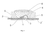
Fig. 1 shows a cross section of an example of an optical semiconductor device. InFig. 1 ,optical semiconductor element 1, such as an LED, is die bonded to leadframe 2 and further wire bonded viabonding wire 3 to lead frame 2'. The space between these semiconductor elements is filled with transparent encapsulatingresin 4. In the example illustrated inFig. 1 , a cured product of the present silicone resin composition is used to preparewhite reflector 5.Numeral 6 indicates a lens. - The reflector thus obtained initially has a light reflectance at a wavelength of 450 nm of 70 % or higher, particularly 80 % or higher, more particularly 85 % or higher. After a degradation test at 180 degrees C for 24 hours, the reflector has a reflectance of 70 % or higher, particularly 80 % or higher, more particularly 85 % or higher. If the reflectance after the degradation test is less than 70 %, the durability as a reflector for an LED semiconductor element is short.
- As the most common molding method of the reflector, mention is made of transfer molding and compression molding. The transfer molding is carried out using a transfer molding machine, preferably at a molding pressure of 5 to 20 N/mm2 at a molding temperature of 120 to 190 degrees C for a molding time of 30 to 500 seconds, particularly at a molding temperature of 150 to 185 degrees C for a molding time of 30 to 180 seconds. In the compression molding, molding is carried out using a compression molding machine, preferably at a molding temperature of 120 to 190 degrees C for a molding time of 30 to 600 seconds, particularly at a temperature of 130 to 160 degrees C for 120 to 300 seconds. In both of the molding methods, post curing may be carried out at a temperature of 150 to 185 degrees C for 2 to 20 hours.
- The silicone resin composition of the present invention thus obtained has good moldability and heat and light resistances, particularly against ultraviolet rays and, therefore, is suitable for a pre-molded package for white, blue, or, further, ultraviolet LED, as well as for a packaging material for solar cells.
- Further, the present invention encompasses a pre-molded package which is prepared by integrally encapsulating, with the present composition, a metal substrate or an organic substrate of matrix array type with a lead part and a pad part thereon, while leaving a position for an LED element to be molded open. The present composition can also be used for encapsulating general purpose semiconductors or various modules to be installed in vehicles.
- The present invention will be explained more in detail in the following Examples and Comparative Examples. However, the present invention shall not be limited to the Examples.
- The raw materials used in the Examples and the Comparative Examples are as follows.
- To a one-liter flask were added 100 grams of metyltrichlorosilane and 200 grams of toluene. To the resulting mixture, was added dropwise a mixture of 8 grams of water and 60 grams of isopropyl alcohol over 5 to 20 hours while keeping the inner temperature at -5 to 0 degrees C by cooling the flask in an ice bath. Then, the mixture was heated at a refluxing temperature for 20 minutes with stirring, and cooled to room temperature, to which 12 grams of water were added dropwise at a temperature below 30 degrees C over 30 minutes and the mixture was stirred for 20 minutes. Further, 25 grams of water were added dropwise and stirred at a temperature of 40 to 45 degrees C for 60 minutes. Then, 200 grams of water were added and an organic phase was separated. The organic phase was washed until the phase became neutral and then subjected to azeotropic dehydration, filtration, and evaporation under reduced pressure to obtain 36.0 grams of a colorless and transparent solid (melting point, 76 degrees C), organopolysiloxane (A) represented by the following formula (8).
- White pigment: titanium dioxide (rutile type), R-45M (ex Sakai Chemical Industry Co., Ltd.), average particle diameter of 0.29µm.
- Spherical fused silica, MSR-4500TN (ex Tatsumori Co., Ltd), average particle diameter of 45 µm.
Spherical silica, SO 25 R (ex Admatechs Co., Ltd), average particle diameter of 0.5µm. - Zinc benzoate, ex Wako Pure Chemical Industries Ltd.
- Triglycidyl isocyanurate, TEPIC, ex Nissan Chemical Industries, Ltd.
- 5.4 Grams (0.03 mole) of phenylmethyldichlorosilane, 114 grams (0.539 mole) of phenyltrichlorosilane, 100 grams (0.066 mole) of a silicone oil having 20 Si atoms and chlorodimethyl groups on both ends and represented by Cl(Me)2SiO(Me2SiO)nSi (Me)2Cl wherein n is 18 on average, 3000 grams of toluene were mixed, added dropwise to 11000 grams of water, and hydrolyzed at a temperature of 30 to 50 degrees C for 1 hour. Then, the mixture was aged at 50 degrees C for 1 hour, to which water was added for washing. Then, the organic phase was subjected to azeotropic dehydration, filtration, and evaporation under reduced pressure to obtain colorless and transparent organopolysiloxane (F) which had a melt viscosity of 5 Pa·s at 150 degrees C and is represented by the following formula (9). The content of the silanol group was 3 mole %.
-

-

-
- (H) Silane coupling agent: KBM803, ex Shin-Etsu Chemical Co., Ltd.
- (I) Wax: Calcium stearate, ex Wako Pure Chemical Industries, Ltd.
- According to the formulations shown in Table 1, organopolysiloxane (A), white pigment (B), inorganic filler (C), curing catalyst (D), epoxy resin (E), organopolysiloxane (F) and linear diorganopolysiloxane (G) were blended and mixed by rolls, cooled and pulverized to obtain white silicone resin compositions.
- The following properties were determined on these compositions. The results are as shown in Table 1.
- Using a mold according to the Epoxy Molding Materials Institute (EMMI) Standards, a spiral flow value was determined at a molding temperature of 175 degrees C and a molding pressure of 6.9 N/mm2 with a molding time of 120 seconds.
- On an Ag-plated substance of a size of 20 x 20 mm, the afore-mentioned resin composition was transfer molded using a mold at 175 degrees C and 6.9 N/mm2 with a molding time of 120 seconds to form a cured resin product in a form of a frustum with a diameter of 2 mm in the upper base, a diameter of 5 mm in the bottom base, and a height of 3 mm to prepare a test piece for the adhesion test. The test piece was postcured at 180 degrees C for 4 hours and the adhesion strength was determined according to the shear adhesion method.
- An MAP type package of 35 x 35 mm (Cu frame) was encapsulated with a resin of 32 X 32 X 1.2 mm at 175 degrees C and 6.9 N/mm2 with a molding time of 120 seconds. The cured product was subjected to a temperature of - 40 degrees C and a temperature of 150 degrees C in 100 cycles and the appearance was observed to visually evaluate existence of cracks (n=8).
- A cured product of 5 x 5 x 15 mm was molded in the conditions of a molding temperature of 175 degrees C, a molding pressure of 6.9 N/mm2, and a molding time of 120 seconds and subjected to post curing at 180 degrees C for 4 hours. Then, a linear expansion coefficient was determined at a temperature rising rate of 5 degrees C / minute with an instrument, TMA 8140 C, ex Rigaku Corporation.
- A disc, cured product of 50 mm in diameter and 3 mm in thickness, was molded in the conditions of a molding temperature of 175 degrees C, a molding pressure of 6.9 N/mm2 and a molding time of 120 seconds. Immediately after the molding, the disc was left at 180 degrees C for 24 hours, and irradiated with UV from a highpressure mercury lamp having a peak wavelength of 365 nm and an output of 60 mW/cm for 24 hours. A light reflectance at wave lengths of 350 to 400 nm was measured using X-rite 8200, ex S. D. G. Co., Ltd.
-

- As seen in Table 1, the adhesion was low in Comparative Example 1, where component (E) was not contained at all. Cracks appeared after temperature cycles in Comparative Example 2 where the content of (G) was too low and Comparative Example 3 where component (G) was not contained at all. Meanwhile, in Comparative Example 4 where component (G) was only one silicone, the flowability was poor, so that the moldability was poor. Contrary to these, the Examples of the present invention showed good adhesion and crack resistance and no decrease in light reflectance.
- The present resin composition is suitable for use in optical semiconductor devices, particularly reflectors.
Claims (3)
- A silicone resin composition, comprising(A) 100 parts by weight of an organopolysiloxane having a weight average molecular weight of from 500 to 20000, reduced to polystyrene, and represented by the following average compositional formula (1),
(CH3)aSi(OR1)b(OH)cO(4-a-b-c)/2 (1)
wherein R1 is a monovalent hydrocarbon group having 1 to 4 carbon atoms and a, b, and c are numbers satisfying the equations: 0.8 <= a <= 1.5, 0 <= b <= 0.3, 0.001 <= c <= 0.5, and 0.801 <= a + b + c <2,(B) 3 to 200 parts by weight of a white pigment,(C) 400 to 1000 parts by weight of an inorganic filler other than the afore-mentioned white pigment,(D) 0.01 to 10 parts by weight of a condensation catalyst,(E) 1.0 to 10 parts by weight of an epoxy resin which is a derivative of isocyanuric acid,(F) 2 to 50 parts by weight of an organopolysiloxane comprising unit R2SiO and unit RSiO1.5, wherein R may be the same or different and is a group selected from the group consisting of a hydroxyl group, a methyl group, an ethyl group, a propyl group, a cyclohexyl group, a phenyl group, a vinyl group and an allyl group, wherein at least a part of the afore-mentioned unit R2SiO repeats itself in series and the number of the repetition is 5 to 100, and wherein 0.5 to 10 mole % of the siloxane units comprising unit R2SiO and unit RSiO1.5 has a silanol group, and(G) 2 to 50 parts by weight of a linear dioraganopolysiloxane represented by the following formula (2).
- The silicone resin composition according to claim 1, wherein
white pigment (B) is at least one selected from the group consisting of titanium dioxide, magnesium oxide and alumina with an average particle diameter of from 0.05 to 10.0 µ m and is present in an amount of 1 to 50 % by weight, relative to the silicone resin composition; and
the total % by weight of white pigment (B) and inorganic filler (C) is 70 to 93 % by weight, relative to the silicone resin composition. - A pre-molded package molded with the silicone resin composition according to claim 1 or 2.
Applications Claiming Priority (1)
| Application Number | Priority Date | Filing Date | Title |
|---|---|---|---|
| JP2009107101A JP5108825B2 (en) | 2009-04-24 | 2009-04-24 | Silicone resin composition for optical semiconductor device and optical semiconductor device |
Publications (2)
| Publication Number | Publication Date |
|---|---|
| EP2253671A1 true EP2253671A1 (en) | 2010-11-24 |
| EP2253671B1 EP2253671B1 (en) | 2012-01-18 |
Family
ID=42289380
Family Applications (1)
| Application Number | Title | Priority Date | Filing Date |
|---|---|---|---|
| EP10160782A Active EP2253671B1 (en) | 2009-04-24 | 2010-04-22 | Silicone Resin Composition for Optical Semiconductor Devices and an Optical Semiconductor Device |
Country Status (7)
| Country | Link |
|---|---|
| US (1) | US8193269B2 (en) |
| EP (1) | EP2253671B1 (en) |
| JP (1) | JP5108825B2 (en) |
| KR (1) | KR101520510B1 (en) |
| CN (1) | CN101870817B (en) |
| AT (1) | ATE541896T1 (en) |
| TW (1) | TWI393747B (en) |
Cited By (3)
| Publication number | Priority date | Publication date | Assignee | Title |
|---|---|---|---|---|
| EP2800154A4 (en) * | 2011-12-26 | 2015-06-10 | Konica Minolta Inc | Sealant for led device, led device, and method for producing led device |
| EP3239245A4 (en) * | 2014-12-25 | 2018-08-22 | Shengyi Technology Co. Ltd. | Organic silicon resin composition, white prepreg and white laminate using same |
| DE102021116584A1 (en) | 2021-06-28 | 2022-12-29 | OSRAM Opto Semiconductors Gesellschaft mit beschränkter Haftung | LIGHT EMITTING DEVICE |
Families Citing this family (39)
| Publication number | Priority date | Publication date | Assignee | Title |
|---|---|---|---|---|
| JP2010106243A (en) * | 2008-09-30 | 2010-05-13 | Shin-Etsu Chemical Co Ltd | Silicone resin composition for optical semiconductor device |
| JP4964928B2 (en) * | 2009-09-15 | 2012-07-04 | 信越化学工業株式会社 | Underfill material composition and optical semiconductor device |
| JP5545246B2 (en) * | 2010-03-30 | 2014-07-09 | 信越化学工業株式会社 | Resin composition, reflector for light emitting semiconductor element, and light emitting semiconductor device |
| JP2012057000A (en) * | 2010-09-07 | 2012-03-22 | Shin-Etsu Chemical Co Ltd | Silicone resin composition, sealing material of semiconductor device, and semiconductor device |
| US9045668B2 (en) * | 2010-09-22 | 2015-06-02 | Dow Corning Corporation | Organosiloxane block copolymer |
| KR101778832B1 (en) * | 2010-11-02 | 2017-09-14 | 다이니폰 인사츠 가부시키가이샤 | Led-element mounting lead frame, resin-attached lead frame, method of manufacturing semiconductor device, and semiconductor-element mounting lead frame |
| WO2012117822A1 (en) * | 2011-02-28 | 2012-09-07 | 横浜ゴム株式会社 | Heat-curable silicone resin composition for optical-semiconductor encapsulation and optical-semiconductor package formed using same |
| TW201238406A (en) * | 2011-03-11 | 2012-09-16 | Ind Tech Res Inst | Light emitting devices |
| TW201300461A (en) * | 2011-06-16 | 2013-01-01 | Nitto Denko Corp | Silicone resin composition, encapsulating layer, reflector, and optical semiconductor device |
| JP2013001824A (en) * | 2011-06-17 | 2013-01-07 | Mitsubishi Chemicals Corp | Silicone resin composition for semiconductor luminescent device |
| JP5880556B2 (en) * | 2011-07-04 | 2016-03-09 | Jnc株式会社 | Compound containing organopolysiloxane or silsesquioxane skeleton having isocyanur skeleton, epoxy group and SiH group, and thermosetting resin composition, cured product, and optical semiconductor encapsulant containing the compound as an adhesion-imparting material |
| WO2013008842A1 (en) * | 2011-07-14 | 2013-01-17 | 積水化学工業株式会社 | Sealing agent for optical semiconductor devices, and optical semiconductor device |
| JP5556794B2 (en) * | 2011-11-21 | 2014-07-23 | 信越化学工業株式会社 | White thermosetting silicone resin composition useful as LED reflector and optical semiconductor device using the composition |
| JP5640957B2 (en) * | 2011-11-21 | 2014-12-17 | 信越化学工業株式会社 | White thermosetting silicone resin composition useful as LED reflector and optical semiconductor device using the composition |
| JP2013133429A (en) * | 2011-12-27 | 2013-07-08 | Kaneka Corp | Resin molding for surface mounting type light emitting device and light emitting device using the same |
| JP2013159670A (en) * | 2012-02-02 | 2013-08-19 | Dow Corning Toray Co Ltd | Curable silicone composition, its cured product, and optical semiconductor device |
| KR20140130161A (en) * | 2012-02-10 | 2014-11-07 | 미쓰비시 쥬시 가부시끼가이샤 | Coverlay film, printed wiring board to be equipped with light-emitting element, and light source device |
| WO2013130574A1 (en) | 2012-02-29 | 2013-09-06 | Dow Corning Corporation | Compositions of resin-linear organosiloxane block copolymers |
| WO2013134018A1 (en) | 2012-03-09 | 2013-09-12 | Dow Corning Corporation | Compositions of resin-linear organosiloxane block copolymers |
| EP2825599A1 (en) * | 2012-03-12 | 2015-01-21 | Dow Corning Corporation | Compositions of resin-linear organosiloxane block copolymers |
| JP5940325B2 (en) * | 2012-03-12 | 2016-06-29 | 東レ・ダウコーニング株式会社 | Thermally conductive silicone composition |
| WO2013142243A2 (en) * | 2012-03-20 | 2013-09-26 | Dow Corning Corporation | Light guide and associated light assemblies |
| CN104245797B (en) | 2012-03-21 | 2017-03-01 | 道康宁公司 | Comprise resin linear Organosiloxane block copolymer and the compositionss of organopolysiloxane |
| JP2015515515A (en) | 2012-03-21 | 2015-05-28 | ダウ コーニング コーポレーションDow Corning Corporation | Process for preparing resin-linear organosiloxane block copolymers |
| JP2015516999A (en) * | 2012-03-21 | 2015-06-18 | ダウ コーニング コーポレーションDow Corning Corporation | Resin-linear organosiloxane block copolymer composition |
| EP2945197A4 (en) * | 2013-01-10 | 2016-08-03 | Konica Minolta Inc | Led device and coating liquid used for production of same |
| WO2014152522A1 (en) | 2013-03-15 | 2014-09-25 | Dow Corning Corporation | Compositions of resin-linear organosiloxane block copolymers |
| WO2014197617A1 (en) | 2013-06-05 | 2014-12-11 | Dow Corning Corporation | Compositions of resin-linear organosiloxane block copolymers |
| WO2015005275A1 (en) * | 2013-07-11 | 2015-01-15 | 住友ベークライト株式会社 | Process for producing semiconductor devices, and semiconductor device |
| JP6311319B2 (en) * | 2014-01-14 | 2018-04-18 | 大日本印刷株式会社 | Resin composition, reflector, lead frame with reflector, and semiconductor light emitting device |
| CN105778506B (en) | 2014-12-25 | 2019-04-30 | 广东生益科技股份有限公司 | A kind of organosilicon resin composition and prepreg, laminate, copper-clad plate and aluminum substrate using it |
| CN104592931B (en) * | 2015-02-12 | 2017-06-06 | 中国工程物理研究院化工材料研究所 | High power LED package glue composition |
| JP6307465B2 (en) | 2015-03-24 | 2018-04-04 | 信越化学工業株式会社 | Condensation-curable silicone composition and semiconductor device |
| JP2017009725A (en) * | 2015-06-19 | 2017-01-12 | ソニー株式会社 | Display device |
| DE112017000390T5 (en) * | 2016-01-15 | 2018-09-27 | Citizen Electronics Co., Ltd. | Condensation reaction type chip binder, LED light emitting device and method of making the same |
| CN106928510A (en) * | 2017-02-23 | 2017-07-07 | 苏州纳贝通环境科技有限公司 | A kind of oil-resisting and heat-resisting elastomeric material and preparation method thereof |
| KR102449295B1 (en) | 2018-05-18 | 2022-09-30 | 롬 앤드 하스 일렉트로닉 머트어리얼즈 엘엘씨 | LED Manufacturing Method by Single Step Film Lamination |
| CN109762167A (en) * | 2018-12-14 | 2019-05-17 | 中国科学院深圳先进技术研究院 | A kind of LED small-size chips heat conductive insulating die bond material and preparation method thereof |
| US20200333702A1 (en) * | 2019-04-19 | 2020-10-22 | Canon Kabushiki Kaisha | Forming apparatus, forming method, and article manufacturing method |
Citations (7)
| Publication number | Priority date | Publication date | Assignee | Title |
|---|---|---|---|---|
| US5530063A (en) * | 1993-06-15 | 1996-06-25 | Shin-Etsu Chemical Co., Ltd. | Room temperature curable organopolysiloxane composition |
| JP2005306952A (en) | 2004-04-20 | 2005-11-04 | Japan Epoxy Resin Kk | Epoxy resin composition as sealing material for light-emitting element |
| US20060204760A1 (en) * | 2005-03-01 | 2006-09-14 | Nitto Denko Corporation | Epoxy resin composition for photosemiconductor element encapsulation and photosemiconductor device using the same |
| US20060229408A1 (en) * | 2005-04-08 | 2006-10-12 | Shin-Etsu Chemical Co., Ltd. | Curable resin composition for sealing LED element |
| JP2009107101A (en) | 2007-11-01 | 2009-05-21 | Mikata:Kk | Reassuring mark |
| EP2141201A1 (en) * | 2008-07-02 | 2010-01-06 | Shin-Etsu Chemical Co., Ltd. | Heat-curable silicone resin-epoxy resin composition, and premolded package molded from same |
| EP2172522A1 (en) * | 2008-06-09 | 2010-04-07 | Shin-Etsu Chemical Co., Ltd. | white heat-curable silicone resin composition and optoelectronic part case |
Family Cites Families (13)
| Publication number | Priority date | Publication date | Assignee | Title |
|---|---|---|---|---|
| JP2656336B2 (en) | 1989-01-18 | 1997-09-24 | 日東電工株式会社 | Optical semiconductor device and epoxy resin composition for encapsulating optical semiconductor used therein |
| CN1178230A (en) * | 1996-07-30 | 1998-04-08 | 日本化药株式会社 | Epoxy resin liquid composition for semiconductor encapsulation |
| JP2006265529A (en) * | 2005-02-28 | 2006-10-05 | Shin Etsu Chem Co Ltd | Room temperature curable organopolysiloxane composition |
| JP4791083B2 (en) * | 2005-05-30 | 2011-10-12 | 信越化学工業株式会社 | Optical composition sealing resin composition and cured product thereof |
| JP4646122B2 (en) * | 2005-06-30 | 2011-03-09 | 信越化学工業株式会社 | Silicone composition for release film |
| JP4514058B2 (en) * | 2006-08-30 | 2010-07-28 | 信越化学工業株式会社 | Thermally conductive silicone composition and cured product thereof |
| JP5176144B2 (en) | 2007-08-22 | 2013-04-03 | 日立化成株式会社 | Thermosetting light reflecting resin composition, substrate for mounting optical semiconductor using the same, method for manufacturing the same, and optical semiconductor device |
| JP4623322B2 (en) * | 2007-12-26 | 2011-02-02 | 信越化学工業株式会社 | White thermosetting silicone resin composition for forming optical semiconductor case, optical semiconductor case and molding method thereof |
| JP4678415B2 (en) * | 2008-03-18 | 2011-04-27 | 信越化学工業株式会社 | White thermosetting silicone resin composition for forming optical semiconductor case and optical semiconductor case |
| JP2010021533A (en) * | 2008-06-09 | 2010-01-28 | Shin-Etsu Chemical Co Ltd | White heat-curable silicone resin composition for forming optical semiconductor case, and optical semiconductor case |
| JP2010106243A (en) * | 2008-09-30 | 2010-05-13 | Shin-Etsu Chemical Co Ltd | Silicone resin composition for optical semiconductor device |
| JP5353629B2 (en) * | 2008-11-14 | 2013-11-27 | 信越化学工業株式会社 | Thermosetting resin composition |
| JP5488326B2 (en) * | 2009-09-01 | 2014-05-14 | 信越化学工業株式会社 | White thermosetting silicone epoxy hybrid resin composition for optical semiconductor device, method for producing the same, pre-mold package and LED device |
-
2009
- 2009-04-24 JP JP2009107101A patent/JP5108825B2/en active Active
-
2010
- 2010-04-15 KR KR1020100034719A patent/KR101520510B1/en active IP Right Grant
- 2010-04-22 EP EP10160782A patent/EP2253671B1/en active Active
- 2010-04-22 AT AT10160782T patent/ATE541896T1/en active
- 2010-04-23 US US12/766,660 patent/US8193269B2/en active Active
- 2010-04-23 CN CN201010155436XA patent/CN101870817B/en active Active
- 2010-04-23 TW TW099112848A patent/TWI393747B/en active
Patent Citations (7)
| Publication number | Priority date | Publication date | Assignee | Title |
|---|---|---|---|---|
| US5530063A (en) * | 1993-06-15 | 1996-06-25 | Shin-Etsu Chemical Co., Ltd. | Room temperature curable organopolysiloxane composition |
| JP2005306952A (en) | 2004-04-20 | 2005-11-04 | Japan Epoxy Resin Kk | Epoxy resin composition as sealing material for light-emitting element |
| US20060204760A1 (en) * | 2005-03-01 | 2006-09-14 | Nitto Denko Corporation | Epoxy resin composition for photosemiconductor element encapsulation and photosemiconductor device using the same |
| US20060229408A1 (en) * | 2005-04-08 | 2006-10-12 | Shin-Etsu Chemical Co., Ltd. | Curable resin composition for sealing LED element |
| JP2009107101A (en) | 2007-11-01 | 2009-05-21 | Mikata:Kk | Reassuring mark |
| EP2172522A1 (en) * | 2008-06-09 | 2010-04-07 | Shin-Etsu Chemical Co., Ltd. | white heat-curable silicone resin composition and optoelectronic part case |
| EP2141201A1 (en) * | 2008-07-02 | 2010-01-06 | Shin-Etsu Chemical Co., Ltd. | Heat-curable silicone resin-epoxy resin composition, and premolded package molded from same |
Non-Patent Citations (1)
| Title |
|---|
| ZHU B ET AL: "Toughening of a polysilsesquioxane network by homogeneous incorporation of polydimethylsiloxane segments", POLYMER, ELSEVIER SCIENCE PUBLISHERS B.V, GB LNKD- DOI:10.1016/S0032-3861(00)00027-6, vol. 41, no. 20, 1 September 2000 (2000-09-01), pages 7559 - 7573, XP004200619, ISSN: 0032-3861 * |
Cited By (4)
| Publication number | Priority date | Publication date | Assignee | Title |
|---|---|---|---|---|
| EP2800154A4 (en) * | 2011-12-26 | 2015-06-10 | Konica Minolta Inc | Sealant for led device, led device, and method for producing led device |
| EP3239245A4 (en) * | 2014-12-25 | 2018-08-22 | Shengyi Technology Co. Ltd. | Organic silicon resin composition, white prepreg and white laminate using same |
| US10336905B2 (en) | 2014-12-25 | 2019-07-02 | Shengyi Technology Co., Ltd. | Organic silicon resin composition, white prepreg and white laminate using same |
| DE102021116584A1 (en) | 2021-06-28 | 2022-12-29 | OSRAM Opto Semiconductors Gesellschaft mit beschränkter Haftung | LIGHT EMITTING DEVICE |
Also Published As
| Publication number | Publication date |
|---|---|
| CN101870817A (en) | 2010-10-27 |
| JP2010254825A (en) | 2010-11-11 |
| EP2253671B1 (en) | 2012-01-18 |
| ATE541896T1 (en) | 2012-02-15 |
| TWI393747B (en) | 2013-04-21 |
| JP5108825B2 (en) | 2012-12-26 |
| TW201038672A (en) | 2010-11-01 |
| KR20100117512A (en) | 2010-11-03 |
| US20100273927A1 (en) | 2010-10-28 |
| CN101870817B (en) | 2013-04-17 |
| KR101520510B1 (en) | 2015-05-14 |
| US8193269B2 (en) | 2012-06-05 |
Similar Documents
| Publication | Publication Date | Title |
|---|---|---|
| EP2253671B1 (en) | Silicone Resin Composition for Optical Semiconductor Devices and an Optical Semiconductor Device | |
| EP2174984B1 (en) | Silicone resin composition for optical semiconductor devices | |
| KR101505626B1 (en) | White heat-curable silicone resin composition, optoelectronic part case, and molding method | |
| EP2135898B1 (en) | White heat-curable silicone resin composition and optoelectronic part case | |
| JP4678415B2 (en) | White thermosetting silicone resin composition for forming optical semiconductor case and optical semiconductor case | |
| EP2295499B1 (en) | Underfill composition and an optical semiconductor device | |
| EP2172522A1 (en) | white heat-curable silicone resin composition and optoelectronic part case | |
| JP5729270B2 (en) | White thermosetting silicone resin composition useful as LED reflector and optical semiconductor device using the composition | |
| JP2011032392A (en) | Silicone resin composition for optical semiconductor apparatus | |
| JP2014177570A (en) | Thermosetting silicone resin composition | |
| JP2012041428A (en) | Silicone resin composition and optical semiconductor case | |
| JP5728960B2 (en) | White thermosetting silicone resin composition for optical semiconductor case formation and optical semiconductor case | |
| JP5246880B2 (en) | Underfill material composition and optical semiconductor device | |
| JP5728961B2 (en) | White thermosetting silicone resin composition for optical semiconductor case formation and optical semiconductor case | |
| JP5556794B2 (en) | White thermosetting silicone resin composition useful as LED reflector and optical semiconductor device using the composition | |
| KR101881604B1 (en) | White thermosetting silicone resin composition useful as led reflector and optical semiconductor device using the same | |
| JP5640957B2 (en) | White thermosetting silicone resin composition useful as LED reflector and optical semiconductor device using the composition | |
| JP2015040238A (en) | Thermosetting silicone resin composition for forming optical semiconductor casing |
Legal Events
| Date | Code | Title | Description |
|---|---|---|---|
| PUAI | Public reference made under article 153(3) epc to a published international application that has entered the european phase |
Free format text: ORIGINAL CODE: 0009012 |
|
| AK | Designated contracting states |
Kind code of ref document: A1 Designated state(s): AT BE BG CH CY CZ DE DK EE ES FI FR GB GR HR HU IE IS IT LI LT LU LV MC MK MT NL NO PL PT RO SE SI SK SM TR |
|
| AX | Request for extension of the european patent |
Extension state: AL BA ME RS |
|
| 17P | Request for examination filed |
Effective date: 20110505 |
|
| RIC1 | Information provided on ipc code assigned before grant |
Ipc: H01L 23/29 20060101ALI20110524BHEP Ipc: H01L 33/56 20100101ALI20110524BHEP Ipc: C09K 3/10 20060101ALI20110524BHEP Ipc: H01L 31/0203 20060101ALI20110524BHEP Ipc: C08L 83/04 20060101AFI20110524BHEP |
|
| GRAP | Despatch of communication of intention to grant a patent |
Free format text: ORIGINAL CODE: EPIDOSNIGR1 |
|
| GRAS | Grant fee paid |
Free format text: ORIGINAL CODE: EPIDOSNIGR3 |
|
| GRAA | (expected) grant |
Free format text: ORIGINAL CODE: 0009210 |
|
| AK | Designated contracting states |
Kind code of ref document: B1 Designated state(s): AT BE BG CH CY CZ DE DK EE ES FI FR GB GR HR HU IE IS IT LI LT LU LV MC MK MT NL NO PL PT RO SE SI SK SM TR |
|
| REG | Reference to a national code |
Ref country code: GB Ref legal event code: FG4D |
|
| REG | Reference to a national code |
Ref country code: CH Ref legal event code: EP |
|
| REG | Reference to a national code |
Ref country code: AT Ref legal event code: REF Ref document number: 541896 Country of ref document: AT Kind code of ref document: T Effective date: 20120215 Ref country code: IE Ref legal event code: FG4D |
|
| REG | Reference to a national code |
Ref country code: DE Ref legal event code: R096 Ref document number: 602010000675 Country of ref document: DE Effective date: 20120322 |
|
| REG | Reference to a national code |
Ref country code: NL Ref legal event code: VDEP Effective date: 20120118 |
|
| LTIE | Lt: invalidation of european patent or patent extension |
Effective date: 20120118 |
|
| PG25 | Lapsed in a contracting state [announced via postgrant information from national office to epo] |
Ref country code: BE Free format text: LAPSE BECAUSE OF FAILURE TO SUBMIT A TRANSLATION OF THE DESCRIPTION OR TO PAY THE FEE WITHIN THE PRESCRIBED TIME-LIMIT Effective date: 20120118 Ref country code: LT Free format text: LAPSE BECAUSE OF FAILURE TO SUBMIT A TRANSLATION OF THE DESCRIPTION OR TO PAY THE FEE WITHIN THE PRESCRIBED TIME-LIMIT Effective date: 20120118 Ref country code: BG Free format text: LAPSE BECAUSE OF FAILURE TO SUBMIT A TRANSLATION OF THE DESCRIPTION OR TO PAY THE FEE WITHIN THE PRESCRIBED TIME-LIMIT Effective date: 20120418 Ref country code: NO Free format text: LAPSE BECAUSE OF FAILURE TO SUBMIT A TRANSLATION OF THE DESCRIPTION OR TO PAY THE FEE WITHIN THE PRESCRIBED TIME-LIMIT Effective date: 20120418 Ref country code: HR Free format text: LAPSE BECAUSE OF FAILURE TO SUBMIT A TRANSLATION OF THE DESCRIPTION OR TO PAY THE FEE WITHIN THE PRESCRIBED TIME-LIMIT Effective date: 20120118 Ref country code: IS Free format text: LAPSE BECAUSE OF FAILURE TO SUBMIT A TRANSLATION OF THE DESCRIPTION OR TO PAY THE FEE WITHIN THE PRESCRIBED TIME-LIMIT Effective date: 20120518 Ref country code: NL Free format text: LAPSE BECAUSE OF FAILURE TO SUBMIT A TRANSLATION OF THE DESCRIPTION OR TO PAY THE FEE WITHIN THE PRESCRIBED TIME-LIMIT Effective date: 20120118 |
|
| PG25 | Lapsed in a contracting state [announced via postgrant information from national office to epo] |
Ref country code: PL Free format text: LAPSE BECAUSE OF FAILURE TO SUBMIT A TRANSLATION OF THE DESCRIPTION OR TO PAY THE FEE WITHIN THE PRESCRIBED TIME-LIMIT Effective date: 20120118 Ref country code: LV Free format text: LAPSE BECAUSE OF FAILURE TO SUBMIT A TRANSLATION OF THE DESCRIPTION OR TO PAY THE FEE WITHIN THE PRESCRIBED TIME-LIMIT Effective date: 20120118 Ref country code: PT Free format text: LAPSE BECAUSE OF FAILURE TO SUBMIT A TRANSLATION OF THE DESCRIPTION OR TO PAY THE FEE WITHIN THE PRESCRIBED TIME-LIMIT Effective date: 20120518 Ref country code: FI Free format text: LAPSE BECAUSE OF FAILURE TO SUBMIT A TRANSLATION OF THE DESCRIPTION OR TO PAY THE FEE WITHIN THE PRESCRIBED TIME-LIMIT Effective date: 20120118 Ref country code: GR Free format text: LAPSE BECAUSE OF FAILURE TO SUBMIT A TRANSLATION OF THE DESCRIPTION OR TO PAY THE FEE WITHIN THE PRESCRIBED TIME-LIMIT Effective date: 20120419 |
|
| REG | Reference to a national code |
Ref country code: AT Ref legal event code: MK05 Ref document number: 541896 Country of ref document: AT Kind code of ref document: T Effective date: 20120118 |
|
| PG25 | Lapsed in a contracting state [announced via postgrant information from national office to epo] |
Ref country code: CY Free format text: LAPSE BECAUSE OF FAILURE TO SUBMIT A TRANSLATION OF THE DESCRIPTION OR TO PAY THE FEE WITHIN THE PRESCRIBED TIME-LIMIT Effective date: 20120118 |
|
| PG25 | Lapsed in a contracting state [announced via postgrant information from national office to epo] |
Ref country code: CZ Free format text: LAPSE BECAUSE OF FAILURE TO SUBMIT A TRANSLATION OF THE DESCRIPTION OR TO PAY THE FEE WITHIN THE PRESCRIBED TIME-LIMIT Effective date: 20120118 Ref country code: RO Free format text: LAPSE BECAUSE OF FAILURE TO SUBMIT A TRANSLATION OF THE DESCRIPTION OR TO PAY THE FEE WITHIN THE PRESCRIBED TIME-LIMIT Effective date: 20120118 Ref country code: SE Free format text: LAPSE BECAUSE OF FAILURE TO SUBMIT A TRANSLATION OF THE DESCRIPTION OR TO PAY THE FEE WITHIN THE PRESCRIBED TIME-LIMIT Effective date: 20120118 Ref country code: EE Free format text: LAPSE BECAUSE OF FAILURE TO SUBMIT A TRANSLATION OF THE DESCRIPTION OR TO PAY THE FEE WITHIN THE PRESCRIBED TIME-LIMIT Effective date: 20120118 Ref country code: DK Free format text: LAPSE BECAUSE OF FAILURE TO SUBMIT A TRANSLATION OF THE DESCRIPTION OR TO PAY THE FEE WITHIN THE PRESCRIBED TIME-LIMIT Effective date: 20120118 Ref country code: SI Free format text: LAPSE BECAUSE OF FAILURE TO SUBMIT A TRANSLATION OF THE DESCRIPTION OR TO PAY THE FEE WITHIN THE PRESCRIBED TIME-LIMIT Effective date: 20120118 |
|
| PLBE | No opposition filed within time limit |
Free format text: ORIGINAL CODE: 0009261 |
|
| STAA | Information on the status of an ep patent application or granted ep patent |
Free format text: STATUS: NO OPPOSITION FILED WITHIN TIME LIMIT |
|
| PG25 | Lapsed in a contracting state [announced via postgrant information from national office to epo] |
Ref country code: IT Free format text: LAPSE BECAUSE OF FAILURE TO SUBMIT A TRANSLATION OF THE DESCRIPTION OR TO PAY THE FEE WITHIN THE PRESCRIBED TIME-LIMIT Effective date: 20120118 Ref country code: MC Free format text: LAPSE BECAUSE OF NON-PAYMENT OF DUE FEES Effective date: 20120430 Ref country code: SK Free format text: LAPSE BECAUSE OF FAILURE TO SUBMIT A TRANSLATION OF THE DESCRIPTION OR TO PAY THE FEE WITHIN THE PRESCRIBED TIME-LIMIT Effective date: 20120118 |
|
| 26N | No opposition filed |
Effective date: 20121019 |
|
| REG | Reference to a national code |
Ref country code: IE Ref legal event code: MM4A |
|
| REG | Reference to a national code |
Ref country code: FR Ref legal event code: ST Effective date: 20121228 |
|
| PG25 | Lapsed in a contracting state [announced via postgrant information from national office to epo] |
Ref country code: IE Free format text: LAPSE BECAUSE OF NON-PAYMENT OF DUE FEES Effective date: 20120422 Ref country code: AT Free format text: LAPSE BECAUSE OF FAILURE TO SUBMIT A TRANSLATION OF THE DESCRIPTION OR TO PAY THE FEE WITHIN THE PRESCRIBED TIME-LIMIT Effective date: 20120118 |
|
| REG | Reference to a national code |
Ref country code: DE Ref legal event code: R097 Ref document number: 602010000675 Country of ref document: DE Effective date: 20121019 |
|
| PG25 | Lapsed in a contracting state [announced via postgrant information from national office to epo] |
Ref country code: FR Free format text: LAPSE BECAUSE OF NON-PAYMENT OF DUE FEES Effective date: 20120430 Ref country code: MK Free format text: LAPSE BECAUSE OF FAILURE TO SUBMIT A TRANSLATION OF THE DESCRIPTION OR TO PAY THE FEE WITHIN THE PRESCRIBED TIME-LIMIT Effective date: 20120118 |
|
| PG25 | Lapsed in a contracting state [announced via postgrant information from national office to epo] |
Ref country code: ES Free format text: LAPSE BECAUSE OF FAILURE TO SUBMIT A TRANSLATION OF THE DESCRIPTION OR TO PAY THE FEE WITHIN THE PRESCRIBED TIME-LIMIT Effective date: 20120429 |
|
| PG25 | Lapsed in a contracting state [announced via postgrant information from national office to epo] |
Ref country code: MT Free format text: LAPSE BECAUSE OF FAILURE TO SUBMIT A TRANSLATION OF THE DESCRIPTION OR TO PAY THE FEE WITHIN THE PRESCRIBED TIME-LIMIT Effective date: 20120118 |
|
| PG25 | Lapsed in a contracting state [announced via postgrant information from national office to epo] |
Ref country code: TR Free format text: LAPSE BECAUSE OF FAILURE TO SUBMIT A TRANSLATION OF THE DESCRIPTION OR TO PAY THE FEE WITHIN THE PRESCRIBED TIME-LIMIT Effective date: 20120118 |
|
| PG25 | Lapsed in a contracting state [announced via postgrant information from national office to epo] |
Ref country code: SM Free format text: LAPSE BECAUSE OF FAILURE TO SUBMIT A TRANSLATION OF THE DESCRIPTION OR TO PAY THE FEE WITHIN THE PRESCRIBED TIME-LIMIT Effective date: 20120118 Ref country code: LU Free format text: LAPSE BECAUSE OF NON-PAYMENT OF DUE FEES Effective date: 20120422 |
|
| PG25 | Lapsed in a contracting state [announced via postgrant information from national office to epo] |
Ref country code: HU Free format text: LAPSE BECAUSE OF FAILURE TO SUBMIT A TRANSLATION OF THE DESCRIPTION OR TO PAY THE FEE WITHIN THE PRESCRIBED TIME-LIMIT Effective date: 20100422 |
|
| REG | Reference to a national code |
Ref country code: CH Ref legal event code: PL |
|
| GBPC | Gb: european patent ceased through non-payment of renewal fee |
Effective date: 20140422 |
|
| PG25 | Lapsed in a contracting state [announced via postgrant information from national office to epo] |
Ref country code: GB Free format text: LAPSE BECAUSE OF NON-PAYMENT OF DUE FEES Effective date: 20140422 Ref country code: LI Free format text: LAPSE BECAUSE OF NON-PAYMENT OF DUE FEES Effective date: 20140430 Ref country code: CH Free format text: LAPSE BECAUSE OF NON-PAYMENT OF DUE FEES Effective date: 20140430 |
|
| PGFP | Annual fee paid to national office [announced via postgrant information from national office to epo] |
Ref country code: DE Payment date: 20230228 Year of fee payment: 14 |