EP2287896A2 - Method for low temperature bonding and bonded structure - Google Patents
Method for low temperature bonding and bonded structure Download PDFInfo
- Publication number
- EP2287896A2 EP2287896A2 EP10185999A EP10185999A EP2287896A2 EP 2287896 A2 EP2287896 A2 EP 2287896A2 EP 10185999 A EP10185999 A EP 10185999A EP 10185999 A EP10185999 A EP 10185999A EP 2287896 A2 EP2287896 A2 EP 2287896A2
- Authority
- EP
- European Patent Office
- Prior art keywords
- bonding
- recited
- item
- wafers
- wafer
- Prior art date
- Legal status (The legal status is an assumption and is not a legal conclusion. Google has not performed a legal analysis and makes no representation as to the accuracy of the status listed.)
- Withdrawn
Links
- 238000000034 method Methods 0.000 title claims abstract description 221
- 239000000463 material Substances 0.000 claims abstract description 99
- 238000005530 etching Methods 0.000 claims abstract description 72
- 230000008569 process Effects 0.000 claims abstract description 68
- 229910052710 silicon Inorganic materials 0.000 claims abstract description 63
- 239000010703 silicon Substances 0.000 claims abstract description 63
- VYPSYNLAJGMNEJ-UHFFFAOYSA-N Silicium dioxide Chemical compound O=[Si]=O VYPSYNLAJGMNEJ-UHFFFAOYSA-N 0.000 claims abstract description 57
- 239000000126 substance Substances 0.000 claims abstract description 31
- 230000003746 surface roughness Effects 0.000 claims abstract description 28
- 230000015572 biosynthetic process Effects 0.000 claims abstract description 8
- 230000004913 activation Effects 0.000 claims abstract description 7
- 238000000137 annealing Methods 0.000 claims description 15
- 229910052814 silicon oxide Inorganic materials 0.000 claims description 14
- IJGRMHOSHXDMSA-UHFFFAOYSA-N Atomic nitrogen Chemical compound N#N IJGRMHOSHXDMSA-UHFFFAOYSA-N 0.000 claims description 6
- YCKRFDGAMUMZLT-UHFFFAOYSA-N Fluorine atom Chemical compound [F] YCKRFDGAMUMZLT-UHFFFAOYSA-N 0.000 claims description 5
- 229910052731 fluorine Inorganic materials 0.000 claims description 5
- 239000011737 fluorine Substances 0.000 claims description 5
- 239000011810 insulating material Substances 0.000 claims description 5
- 229910052757 nitrogen Inorganic materials 0.000 claims description 3
- 230000002708 enhancing effect Effects 0.000 claims 4
- XUIMIQQOPSSXEZ-UHFFFAOYSA-N Silicon Chemical compound [Si] XUIMIQQOPSSXEZ-UHFFFAOYSA-N 0.000 abstract description 60
- 239000006227 byproduct Substances 0.000 abstract description 22
- 239000000377 silicon dioxide Substances 0.000 abstract description 22
- 238000004140 cleaning Methods 0.000 abstract description 16
- VHUUQVKOLVNVRT-UHFFFAOYSA-N Ammonium hydroxide Chemical compound [NH4+].[OH-] VHUUQVKOLVNVRT-UHFFFAOYSA-N 0.000 abstract description 14
- 229910052681 coesite Inorganic materials 0.000 abstract description 11
- 229910052906 cristobalite Inorganic materials 0.000 abstract description 11
- 229910052682 stishovite Inorganic materials 0.000 abstract description 11
- 229910052905 tridymite Inorganic materials 0.000 abstract description 11
- 229910052581 Si3N4 Inorganic materials 0.000 abstract description 10
- HQVNEWCFYHHQES-UHFFFAOYSA-N silicon nitride Chemical compound N12[Si]34N5[Si]62N3[Si]51N64 HQVNEWCFYHHQES-UHFFFAOYSA-N 0.000 abstract description 10
- 238000006116 polymerization reaction Methods 0.000 abstract description 8
- 239000000908 ammonium hydroxide Substances 0.000 abstract description 4
- 230000002441 reversible effect Effects 0.000 abstract description 4
- DDFHBQSCUXNBSA-UHFFFAOYSA-N 5-(5-carboxythiophen-2-yl)thiophene-2-carboxylic acid Chemical compound S1C(C(=O)O)=CC=C1C1=CC=C(C(O)=O)S1 DDFHBQSCUXNBSA-UHFFFAOYSA-N 0.000 abstract description 3
- 238000001020 plasma etching Methods 0.000 abstract description 2
- 238000001039 wet etching Methods 0.000 abstract 1
- 235000012431 wafers Nutrition 0.000 description 239
- 239000010410 layer Substances 0.000 description 110
- 239000000758 substrate Substances 0.000 description 37
- 238000005498 polishing Methods 0.000 description 34
- 239000000243 solution Substances 0.000 description 29
- 239000004065 semiconductor Substances 0.000 description 25
- XLYOFNOQVPJJNP-UHFFFAOYSA-N water Substances O XLYOFNOQVPJJNP-UHFFFAOYSA-N 0.000 description 18
- QGZKDVFQNNGYKY-UHFFFAOYSA-N Ammonia Chemical compound N QGZKDVFQNNGYKY-UHFFFAOYSA-N 0.000 description 17
- 238000000623 plasma-assisted chemical vapour deposition Methods 0.000 description 17
- 238000000151 deposition Methods 0.000 description 15
- 230000001788 irregular Effects 0.000 description 15
- 239000007789 gas Substances 0.000 description 14
- 238000003860 storage Methods 0.000 description 14
- XKRFYHLGVUSROY-UHFFFAOYSA-N Argon Chemical compound [Ar] XKRFYHLGVUSROY-UHFFFAOYSA-N 0.000 description 12
- QVGXLLKOCUKJST-UHFFFAOYSA-N atomic oxygen Chemical compound [O] QVGXLLKOCUKJST-UHFFFAOYSA-N 0.000 description 12
- 238000006243 chemical reaction Methods 0.000 description 12
- 230000002950 deficient Effects 0.000 description 12
- 239000001301 oxygen Substances 0.000 description 12
- 229910052760 oxygen Inorganic materials 0.000 description 12
- 238000005516 engineering process Methods 0.000 description 11
- 238000009832 plasma treatment Methods 0.000 description 11
- 235000012239 silicon dioxide Nutrition 0.000 description 11
- 239000003570 air Substances 0.000 description 10
- LDDQLRUQCUTJBB-UHFFFAOYSA-N ammonium fluoride Chemical compound [NH4+].[F-] LDDQLRUQCUTJBB-UHFFFAOYSA-N 0.000 description 9
- 230000003213 activating effect Effects 0.000 description 8
- 125000004429 atom Chemical group 0.000 description 8
- 239000008367 deionised water Substances 0.000 description 8
- 238000001035 drying Methods 0.000 description 8
- 239000001257 hydrogen Substances 0.000 description 7
- 229910052739 hydrogen Inorganic materials 0.000 description 7
- 125000005647 linker group Chemical group 0.000 description 7
- 239000002356 single layer Substances 0.000 description 7
- 229910052786 argon Inorganic materials 0.000 description 6
- 238000007654 immersion Methods 0.000 description 6
- 229910000069 nitrogen hydride Inorganic materials 0.000 description 6
- 238000012545 processing Methods 0.000 description 6
- 238000004544 sputter deposition Methods 0.000 description 6
- 229910008051 Si-OH Inorganic materials 0.000 description 5
- 229910006358 Si—OH Inorganic materials 0.000 description 5
- 238000001994 activation Methods 0.000 description 5
- 229910021529 ammonia Inorganic materials 0.000 description 5
- 229910021641 deionized water Inorganic materials 0.000 description 5
- 238000010586 diagram Methods 0.000 description 5
- 239000003989 dielectric material Substances 0.000 description 5
- 125000001153 fluoro group Chemical group F* 0.000 description 5
- 229920000642 polymer Polymers 0.000 description 5
- 125000005372 silanol group Chemical group 0.000 description 5
- 238000011282 treatment Methods 0.000 description 5
- UFHFLCQGNIYNRP-UHFFFAOYSA-N Hydrogen Chemical compound [H][H] UFHFLCQGNIYNRP-UHFFFAOYSA-N 0.000 description 4
- GRYLNZFGIOXLOG-UHFFFAOYSA-N Nitric acid Chemical compound O[N+]([O-])=O GRYLNZFGIOXLOG-UHFFFAOYSA-N 0.000 description 4
- 238000009792 diffusion process Methods 0.000 description 4
- 238000009616 inductively coupled plasma Methods 0.000 description 4
- 238000004519 manufacturing process Methods 0.000 description 4
- 238000005259 measurement Methods 0.000 description 4
- 229910017604 nitric acid Inorganic materials 0.000 description 4
- TXEYQDLBPFQVAA-UHFFFAOYSA-N tetrafluoromethane Chemical compound FC(F)(F)F TXEYQDLBPFQVAA-UHFFFAOYSA-N 0.000 description 4
- 238000013459 approach Methods 0.000 description 3
- 238000003486 chemical etching Methods 0.000 description 3
- 238000007598 dipping method Methods 0.000 description 3
- 239000000203 mixture Substances 0.000 description 3
- 239000002344 surface layer Substances 0.000 description 3
- 238000012546 transfer Methods 0.000 description 3
- 102100021765 E3 ubiquitin-protein ligase RNF139 Human genes 0.000 description 2
- 229910001218 Gallium arsenide Inorganic materials 0.000 description 2
- 101001106970 Homo sapiens E3 ubiquitin-protein ligase RNF139 Proteins 0.000 description 2
- 229910002808 Si–O–Si Inorganic materials 0.000 description 2
- 229910008284 Si—F Inorganic materials 0.000 description 2
- 239000012790 adhesive layer Substances 0.000 description 2
- 239000012080 ambient air Substances 0.000 description 2
- 229910021417 amorphous silicon Inorganic materials 0.000 description 2
- 230000008859 change Effects 0.000 description 2
- 238000005229 chemical vapour deposition Methods 0.000 description 2
- 230000007547 defect Effects 0.000 description 2
- 238000010494 dissociation reaction Methods 0.000 description 2
- 230000005593 dissociations Effects 0.000 description 2
- 230000000694 effects Effects 0.000 description 2
- 125000004435 hydrogen atom Chemical group [H]* 0.000 description 2
- 239000012212 insulator Substances 0.000 description 2
- 150000002500 ions Chemical class 0.000 description 2
- 238000012986 modification Methods 0.000 description 2
- 230000004048 modification Effects 0.000 description 2
- 230000001902 propagating effect Effects 0.000 description 2
- 238000001055 reflectance spectroscopy Methods 0.000 description 2
- 235000019592 roughness Nutrition 0.000 description 2
- 238000001004 secondary ion mass spectrometry Methods 0.000 description 2
- 239000007787 solid Substances 0.000 description 2
- 125000006850 spacer group Chemical group 0.000 description 2
- 238000000992 sputter etching Methods 0.000 description 2
- 238000012876 topography Methods 0.000 description 2
- ZOXJGFHDIHLPTG-UHFFFAOYSA-N Boron Chemical compound [B] ZOXJGFHDIHLPTG-UHFFFAOYSA-N 0.000 description 1
- OKTJSMMVPCPJKN-UHFFFAOYSA-N Carbon Chemical compound [C] OKTJSMMVPCPJKN-UHFFFAOYSA-N 0.000 description 1
- 229910004312 HN4F Inorganic materials 0.000 description 1
- 229910014299 N-Si Inorganic materials 0.000 description 1
- NBIIXXVUZAFLBC-UHFFFAOYSA-N Phosphoric acid Chemical compound OP(O)(O)=O NBIIXXVUZAFLBC-UHFFFAOYSA-N 0.000 description 1
- 239000004642 Polyimide Substances 0.000 description 1
- 229910008072 Si-N-Si Inorganic materials 0.000 description 1
- 239000000853 adhesive Substances 0.000 description 1
- 230000001070 adhesive effect Effects 0.000 description 1
- PNEYBMLMFCGWSK-UHFFFAOYSA-N aluminium oxide Inorganic materials [O-2].[O-2].[O-2].[Al+3].[Al+3] PNEYBMLMFCGWSK-UHFFFAOYSA-N 0.000 description 1
- 239000007864 aqueous solution Substances 0.000 description 1
- 238000006664 bond formation reaction Methods 0.000 description 1
- 229910052796 boron Inorganic materials 0.000 description 1
- 229910052799 carbon Inorganic materials 0.000 description 1
- 238000001311 chemical methods and process Methods 0.000 description 1
- 230000003749 cleanliness Effects 0.000 description 1
- 239000000356 contaminant Substances 0.000 description 1
- 238000011109 contamination Methods 0.000 description 1
- 238000001816 cooling Methods 0.000 description 1
- PMHQVHHXPFUNSP-UHFFFAOYSA-M copper(1+);methylsulfanylmethane;bromide Chemical compound Br[Cu].CSC PMHQVHHXPFUNSP-UHFFFAOYSA-M 0.000 description 1
- 229910052593 corundum Inorganic materials 0.000 description 1
- 230000001419 dependent effect Effects 0.000 description 1
- 238000013461 design Methods 0.000 description 1
- 238000004090 dissolution Methods 0.000 description 1
- 230000005684 electric field Effects 0.000 description 1
- 238000001704 evaporation Methods 0.000 description 1
- 230000008020 evaporation Effects 0.000 description 1
- 230000004927 fusion Effects 0.000 description 1
- 238000009499 grossing Methods 0.000 description 1
- 238000010438 heat treatment Methods 0.000 description 1
- 238000002173 high-resolution transmission electron microscopy Methods 0.000 description 1
- 230000005661 hydrophobic surface Effects 0.000 description 1
- 238000011065 in-situ storage Methods 0.000 description 1
- 238000007689 inspection Methods 0.000 description 1
- 238000009413 insulation Methods 0.000 description 1
- 238000005304 joining Methods 0.000 description 1
- 238000001459 lithography Methods 0.000 description 1
- 230000000873 masking effect Effects 0.000 description 1
- 230000013011 mating Effects 0.000 description 1
- 230000007246 mechanism Effects 0.000 description 1
- 229910003465 moissanite Inorganic materials 0.000 description 1
- 230000003647 oxidation Effects 0.000 description 1
- 238000007254 oxidation reaction Methods 0.000 description 1
- 239000002245 particle Substances 0.000 description 1
- 238000002161 passivation Methods 0.000 description 1
- 235000011007 phosphoric acid Nutrition 0.000 description 1
- 229920001721 polyimide Polymers 0.000 description 1
- 239000002861 polymer material Substances 0.000 description 1
- 239000000843 powder Substances 0.000 description 1
- 229910052594 sapphire Inorganic materials 0.000 description 1
- 239000010980 sapphire Substances 0.000 description 1
- 238000000926 separation method Methods 0.000 description 1
- 229910010271 silicon carbide Inorganic materials 0.000 description 1
- 238000001179 sorption measurement Methods 0.000 description 1
- 230000002269 spontaneous effect Effects 0.000 description 1
- 238000006467 substitution reaction Methods 0.000 description 1
- 238000006557 surface reaction Methods 0.000 description 1
- 238000005382 thermal cycling Methods 0.000 description 1
- 229910001845 yogo sapphire Inorganic materials 0.000 description 1
Images


Classifications
-
- H—ELECTRICITY
- H01—ELECTRIC ELEMENTS
- H01L—SEMICONDUCTOR DEVICES NOT COVERED BY CLASS H10
- H01L24/00—Arrangements for connecting or disconnecting semiconductor or solid-state bodies; Methods or apparatus related thereto
- H01L24/80—Methods for connecting semiconductor or other solid state bodies using means for bonding being attached to, or being formed on, the surface to be connected
- H01L24/83—Methods for connecting semiconductor or other solid state bodies using means for bonding being attached to, or being formed on, the surface to be connected using a layer connector
-
- H—ELECTRICITY
- H01—ELECTRIC ELEMENTS
- H01L—SEMICONDUCTOR DEVICES NOT COVERED BY CLASS H10
- H01L21/00—Processes or apparatus adapted for the manufacture or treatment of semiconductor or solid state devices or of parts thereof
- H01L21/02—Manufacture or treatment of semiconductor devices or of parts thereof
- H01L21/04—Manufacture or treatment of semiconductor devices or of parts thereof the devices having at least one potential-jump barrier or surface barrier, e.g. PN junction, depletion layer or carrier concentration layer
- H01L21/18—Manufacture or treatment of semiconductor devices or of parts thereof the devices having at least one potential-jump barrier or surface barrier, e.g. PN junction, depletion layer or carrier concentration layer the devices having semiconductor bodies comprising elements of Group IV of the Periodic System or AIIIBV compounds with or without impurities, e.g. doping materials
- H01L21/30—Treatment of semiconductor bodies using processes or apparatus not provided for in groups H01L21/20 - H01L21/26
- H01L21/302—Treatment of semiconductor bodies using processes or apparatus not provided for in groups H01L21/20 - H01L21/26 to change their surface-physical characteristics or shape, e.g. etching, polishing, cutting
- H01L21/306—Chemical or electrical treatment, e.g. electrolytic etching
- H01L21/3063—Electrolytic etching
-
- H—ELECTRICITY
- H01—ELECTRIC ELEMENTS
- H01L—SEMICONDUCTOR DEVICES NOT COVERED BY CLASS H10
- H01L21/00—Processes or apparatus adapted for the manufacture or treatment of semiconductor or solid state devices or of parts thereof
- H01L21/02—Manufacture or treatment of semiconductor devices or of parts thereof
- H01L21/02041—Cleaning
- H01L21/02057—Cleaning during device manufacture
- H01L21/0206—Cleaning during device manufacture during, before or after processing of insulating layers
-
- H—ELECTRICITY
- H01—ELECTRIC ELEMENTS
- H01L—SEMICONDUCTOR DEVICES NOT COVERED BY CLASS H10
- H01L21/00—Processes or apparatus adapted for the manufacture or treatment of semiconductor or solid state devices or of parts thereof
- H01L21/02—Manufacture or treatment of semiconductor devices or of parts thereof
- H01L21/04—Manufacture or treatment of semiconductor devices or of parts thereof the devices having at least one potential-jump barrier or surface barrier, e.g. PN junction, depletion layer or carrier concentration layer
- H01L21/18—Manufacture or treatment of semiconductor devices or of parts thereof the devices having at least one potential-jump barrier or surface barrier, e.g. PN junction, depletion layer or carrier concentration layer the devices having semiconductor bodies comprising elements of Group IV of the Periodic System or AIIIBV compounds with or without impurities, e.g. doping materials
- H01L21/20—Deposition of semiconductor materials on a substrate, e.g. epitaxial growth solid phase epitaxy
- H01L21/2003—Deposition of semiconductor materials on a substrate, e.g. epitaxial growth solid phase epitaxy characterised by the substrate
- H01L21/2007—Bonding of semiconductor wafers to insulating substrates or to semiconducting substrates using an intermediate insulating layer
-
- H—ELECTRICITY
- H01—ELECTRIC ELEMENTS
- H01L—SEMICONDUCTOR DEVICES NOT COVERED BY CLASS H10
- H01L21/00—Processes or apparatus adapted for the manufacture or treatment of semiconductor or solid state devices or of parts thereof
- H01L21/02—Manufacture or treatment of semiconductor devices or of parts thereof
- H01L21/04—Manufacture or treatment of semiconductor devices or of parts thereof the devices having at least one potential-jump barrier or surface barrier, e.g. PN junction, depletion layer or carrier concentration layer
- H01L21/18—Manufacture or treatment of semiconductor devices or of parts thereof the devices having at least one potential-jump barrier or surface barrier, e.g. PN junction, depletion layer or carrier concentration layer the devices having semiconductor bodies comprising elements of Group IV of the Periodic System or AIIIBV compounds with or without impurities, e.g. doping materials
- H01L21/30—Treatment of semiconductor bodies using processes or apparatus not provided for in groups H01L21/20 - H01L21/26
- H01L21/31—Treatment of semiconductor bodies using processes or apparatus not provided for in groups H01L21/20 - H01L21/26 to form insulating layers thereon, e.g. for masking or by using photolithographic techniques; After treatment of these layers; Selection of materials for these layers
- H01L21/3105—After-treatment
- H01L21/311—Etching the insulating layers by chemical or physical means
- H01L21/31105—Etching inorganic layers
- H01L21/31111—Etching inorganic layers by chemical means
- H01L21/31116—Etching inorganic layers by chemical means by dry-etching
-
- H—ELECTRICITY
- H01—ELECTRIC ELEMENTS
- H01L—SEMICONDUCTOR DEVICES NOT COVERED BY CLASS H10
- H01L21/00—Processes or apparatus adapted for the manufacture or treatment of semiconductor or solid state devices or of parts thereof
- H01L21/02—Manufacture or treatment of semiconductor devices or of parts thereof
- H01L21/04—Manufacture or treatment of semiconductor devices or of parts thereof the devices having at least one potential-jump barrier or surface barrier, e.g. PN junction, depletion layer or carrier concentration layer
- H01L21/18—Manufacture or treatment of semiconductor devices or of parts thereof the devices having at least one potential-jump barrier or surface barrier, e.g. PN junction, depletion layer or carrier concentration layer the devices having semiconductor bodies comprising elements of Group IV of the Periodic System or AIIIBV compounds with or without impurities, e.g. doping materials
- H01L21/30—Treatment of semiconductor bodies using processes or apparatus not provided for in groups H01L21/20 - H01L21/26
- H01L21/322—Treatment of semiconductor bodies using processes or apparatus not provided for in groups H01L21/20 - H01L21/26 to modify their internal properties, e.g. to produce internal imperfections
-
- H—ELECTRICITY
- H01—ELECTRIC ELEMENTS
- H01L—SEMICONDUCTOR DEVICES NOT COVERED BY CLASS H10
- H01L21/00—Processes or apparatus adapted for the manufacture or treatment of semiconductor or solid state devices or of parts thereof
- H01L21/70—Manufacture or treatment of devices consisting of a plurality of solid state components formed in or on a common substrate or of parts thereof; Manufacture of integrated circuit devices or of parts thereof
- H01L21/71—Manufacture of specific parts of devices defined in group H01L21/70
- H01L21/76—Making of isolation regions between components
- H01L21/762—Dielectric regions, e.g. EPIC dielectric isolation, LOCOS; Trench refilling techniques, SOI technology, use of channel stoppers
- H01L21/7624—Dielectric regions, e.g. EPIC dielectric isolation, LOCOS; Trench refilling techniques, SOI technology, use of channel stoppers using semiconductor on insulator [SOI] technology
- H01L21/76251—Dielectric regions, e.g. EPIC dielectric isolation, LOCOS; Trench refilling techniques, SOI technology, use of channel stoppers using semiconductor on insulator [SOI] technology using bonding techniques
-
- H—ELECTRICITY
- H01—ELECTRIC ELEMENTS
- H01L—SEMICONDUCTOR DEVICES NOT COVERED BY CLASS H10
- H01L24/00—Arrangements for connecting or disconnecting semiconductor or solid-state bodies; Methods or apparatus related thereto
- H01L24/01—Means for bonding being attached to, or being formed on, the surface to be connected, e.g. chip-to-package, die-attach, "first-level" interconnects; Manufacturing methods related thereto
- H01L24/26—Layer connectors, e.g. plate connectors, solder or adhesive layers; Manufacturing methods related thereto
-
- H—ELECTRICITY
- H01—ELECTRIC ELEMENTS
- H01L—SEMICONDUCTOR DEVICES NOT COVERED BY CLASS H10
- H01L24/00—Arrangements for connecting or disconnecting semiconductor or solid-state bodies; Methods or apparatus related thereto
- H01L24/74—Apparatus for manufacturing arrangements for connecting or disconnecting semiconductor or solid-state bodies
- H01L24/75—Apparatus for connecting with bump connectors or layer connectors
-
- H—ELECTRICITY
- H01—ELECTRIC ELEMENTS
- H01L—SEMICONDUCTOR DEVICES NOT COVERED BY CLASS H10
- H01L25/00—Assemblies consisting of a plurality of individual semiconductor or other solid state devices ; Multistep manufacturing processes thereof
- H01L25/03—Assemblies consisting of a plurality of individual semiconductor or other solid state devices ; Multistep manufacturing processes thereof all the devices being of a type provided for in the same subgroup of groups H01L27/00 - H01L33/00, or in a single subclass of H10K, H10N, e.g. assemblies of rectifier diodes
- H01L25/04—Assemblies consisting of a plurality of individual semiconductor or other solid state devices ; Multistep manufacturing processes thereof all the devices being of a type provided for in the same subgroup of groups H01L27/00 - H01L33/00, or in a single subclass of H10K, H10N, e.g. assemblies of rectifier diodes the devices not having separate containers
- H01L25/065—Assemblies consisting of a plurality of individual semiconductor or other solid state devices ; Multistep manufacturing processes thereof all the devices being of a type provided for in the same subgroup of groups H01L27/00 - H01L33/00, or in a single subclass of H10K, H10N, e.g. assemblies of rectifier diodes the devices not having separate containers the devices being of a type provided for in group H01L27/00
- H01L25/0657—Stacked arrangements of devices
-
- H—ELECTRICITY
- H01—ELECTRIC ELEMENTS
- H01L—SEMICONDUCTOR DEVICES NOT COVERED BY CLASS H10
- H01L25/00—Assemblies consisting of a plurality of individual semiconductor or other solid state devices ; Multistep manufacturing processes thereof
- H01L25/50—Multistep manufacturing processes of assemblies consisting of devices, each device being of a type provided for in group H01L27/00 or H01L29/00
-
- H—ELECTRICITY
- H01—ELECTRIC ELEMENTS
- H01L—SEMICONDUCTOR DEVICES NOT COVERED BY CLASS H10
- H01L27/00—Devices consisting of a plurality of semiconductor or other solid-state components formed in or on a common substrate
- H01L27/02—Devices consisting of a plurality of semiconductor or other solid-state components formed in or on a common substrate including semiconductor components specially adapted for rectifying, oscillating, amplifying or switching and having at least one potential-jump barrier or surface barrier; including integrated passive circuit elements with at least one potential-jump barrier or surface barrier
- H01L27/04—Devices consisting of a plurality of semiconductor or other solid-state components formed in or on a common substrate including semiconductor components specially adapted for rectifying, oscillating, amplifying or switching and having at least one potential-jump barrier or surface barrier; including integrated passive circuit elements with at least one potential-jump barrier or surface barrier the substrate being a semiconductor body
- H01L27/08—Devices consisting of a plurality of semiconductor or other solid-state components formed in or on a common substrate including semiconductor components specially adapted for rectifying, oscillating, amplifying or switching and having at least one potential-jump barrier or surface barrier; including integrated passive circuit elements with at least one potential-jump barrier or surface barrier the substrate being a semiconductor body including only semiconductor components of a single kind
- H01L27/085—Devices consisting of a plurality of semiconductor or other solid-state components formed in or on a common substrate including semiconductor components specially adapted for rectifying, oscillating, amplifying or switching and having at least one potential-jump barrier or surface barrier; including integrated passive circuit elements with at least one potential-jump barrier or surface barrier the substrate being a semiconductor body including only semiconductor components of a single kind including field-effect components only
-
- H—ELECTRICITY
- H01—ELECTRIC ELEMENTS
- H01L—SEMICONDUCTOR DEVICES NOT COVERED BY CLASS H10
- H01L29/00—Semiconductor devices adapted for rectifying, amplifying, oscillating or switching, or capacitors or resistors with at least one potential-jump barrier or surface barrier, e.g. PN junction depletion layer or carrier concentration layer; Details of semiconductor bodies or of electrodes thereof ; Multistep manufacturing processes therefor
- H01L29/02—Semiconductor bodies ; Multistep manufacturing processes therefor
- H01L29/06—Semiconductor bodies ; Multistep manufacturing processes therefor characterised by their shape; characterised by the shapes, relative sizes, or dispositions of the semiconductor regions ; characterised by the concentration or distribution of impurities within semiconductor regions
-
- H—ELECTRICITY
- H01—ELECTRIC ELEMENTS
- H01L—SEMICONDUCTOR DEVICES NOT COVERED BY CLASS H10
- H01L29/00—Semiconductor devices adapted for rectifying, amplifying, oscillating or switching, or capacitors or resistors with at least one potential-jump barrier or surface barrier, e.g. PN junction depletion layer or carrier concentration layer; Details of semiconductor bodies or of electrodes thereof ; Multistep manufacturing processes therefor
- H01L29/02—Semiconductor bodies ; Multistep manufacturing processes therefor
- H01L29/12—Semiconductor bodies ; Multistep manufacturing processes therefor characterised by the materials of which they are formed
- H01L29/16—Semiconductor bodies ; Multistep manufacturing processes therefor characterised by the materials of which they are formed including, apart from doping materials or other impurities, only elements of Group IV of the Periodic System
-
- H—ELECTRICITY
- H01—ELECTRIC ELEMENTS
- H01L—SEMICONDUCTOR DEVICES NOT COVERED BY CLASS H10
- H01L2224/00—Indexing scheme for arrangements for connecting or disconnecting semiconductor or solid-state bodies and methods related thereto as covered by H01L24/00
- H01L2224/80—Methods for connecting semiconductor or other solid state bodies using means for bonding being attached to, or being formed on, the surface to be connected
- H01L2224/83—Methods for connecting semiconductor or other solid state bodies using means for bonding being attached to, or being formed on, the surface to be connected using a layer connector
- H01L2224/83009—Pre-treatment of the layer connector or the bonding area
- H01L2224/8301—Cleaning the layer connector, e.g. oxide removal step, desmearing
-
- H—ELECTRICITY
- H01—ELECTRIC ELEMENTS
- H01L—SEMICONDUCTOR DEVICES NOT COVERED BY CLASS H10
- H01L2224/00—Indexing scheme for arrangements for connecting or disconnecting semiconductor or solid-state bodies and methods related thereto as covered by H01L24/00
- H01L2224/80—Methods for connecting semiconductor or other solid state bodies using means for bonding being attached to, or being formed on, the surface to be connected
- H01L2224/83—Methods for connecting semiconductor or other solid state bodies using means for bonding being attached to, or being formed on, the surface to be connected using a layer connector
- H01L2224/83009—Pre-treatment of the layer connector or the bonding area
- H01L2224/8303—Reshaping the layer connector in the bonding apparatus, e.g. flattening the layer connector
- H01L2224/83031—Reshaping the layer connector in the bonding apparatus, e.g. flattening the layer connector by chemical means, e.g. etching, anodisation
-
- H—ELECTRICITY
- H01—ELECTRIC ELEMENTS
- H01L—SEMICONDUCTOR DEVICES NOT COVERED BY CLASS H10
- H01L2224/00—Indexing scheme for arrangements for connecting or disconnecting semiconductor or solid-state bodies and methods related thereto as covered by H01L24/00
- H01L2224/80—Methods for connecting semiconductor or other solid state bodies using means for bonding being attached to, or being formed on, the surface to be connected
- H01L2224/83—Methods for connecting semiconductor or other solid state bodies using means for bonding being attached to, or being formed on, the surface to be connected using a layer connector
- H01L2224/83053—Bonding environment
- H01L2224/8309—Vacuum
-
- H—ELECTRICITY
- H01—ELECTRIC ELEMENTS
- H01L—SEMICONDUCTOR DEVICES NOT COVERED BY CLASS H10
- H01L2224/00—Indexing scheme for arrangements for connecting or disconnecting semiconductor or solid-state bodies and methods related thereto as covered by H01L24/00
- H01L2224/80—Methods for connecting semiconductor or other solid state bodies using means for bonding being attached to, or being formed on, the surface to be connected
- H01L2224/83—Methods for connecting semiconductor or other solid state bodies using means for bonding being attached to, or being formed on, the surface to be connected using a layer connector
- H01L2224/83053—Bonding environment
- H01L2224/83095—Temperature settings
- H01L2224/83099—Ambient temperature
-
- H—ELECTRICITY
- H01—ELECTRIC ELEMENTS
- H01L—SEMICONDUCTOR DEVICES NOT COVERED BY CLASS H10
- H01L2224/00—Indexing scheme for arrangements for connecting or disconnecting semiconductor or solid-state bodies and methods related thereto as covered by H01L24/00
- H01L2224/80—Methods for connecting semiconductor or other solid state bodies using means for bonding being attached to, or being formed on, the surface to be connected
- H01L2224/83—Methods for connecting semiconductor or other solid state bodies using means for bonding being attached to, or being formed on, the surface to be connected using a layer connector
- H01L2224/8319—Arrangement of the layer connectors prior to mounting
-
- H—ELECTRICITY
- H01—ELECTRIC ELEMENTS
- H01L—SEMICONDUCTOR DEVICES NOT COVERED BY CLASS H10
- H01L2224/00—Indexing scheme for arrangements for connecting or disconnecting semiconductor or solid-state bodies and methods related thereto as covered by H01L24/00
- H01L2224/80—Methods for connecting semiconductor or other solid state bodies using means for bonding being attached to, or being formed on, the surface to be connected
- H01L2224/83—Methods for connecting semiconductor or other solid state bodies using means for bonding being attached to, or being formed on, the surface to be connected using a layer connector
- H01L2224/838—Bonding techniques
- H01L2224/8385—Bonding techniques using a polymer adhesive, e.g. an adhesive based on silicone, epoxy, polyimide, polyester
-
- H—ELECTRICITY
- H01—ELECTRIC ELEMENTS
- H01L—SEMICONDUCTOR DEVICES NOT COVERED BY CLASS H10
- H01L2224/00—Indexing scheme for arrangements for connecting or disconnecting semiconductor or solid-state bodies and methods related thereto as covered by H01L24/00
- H01L2224/80—Methods for connecting semiconductor or other solid state bodies using means for bonding being attached to, or being formed on, the surface to be connected
- H01L2224/83—Methods for connecting semiconductor or other solid state bodies using means for bonding being attached to, or being formed on, the surface to be connected using a layer connector
- H01L2224/838—Bonding techniques
- H01L2224/83894—Direct bonding, i.e. joining surfaces by means of intermolecular attracting interactions at their interfaces, e.g. covalent bonds, van der Waals forces
- H01L2224/83896—Direct bonding, i.e. joining surfaces by means of intermolecular attracting interactions at their interfaces, e.g. covalent bonds, van der Waals forces between electrically insulating surfaces, e.g. oxide or nitride layers
-
- H—ELECTRICITY
- H01—ELECTRIC ELEMENTS
- H01L—SEMICONDUCTOR DEVICES NOT COVERED BY CLASS H10
- H01L2224/00—Indexing scheme for arrangements for connecting or disconnecting semiconductor or solid-state bodies and methods related thereto as covered by H01L24/00
- H01L2224/80—Methods for connecting semiconductor or other solid state bodies using means for bonding being attached to, or being formed on, the surface to be connected
- H01L2224/83—Methods for connecting semiconductor or other solid state bodies using means for bonding being attached to, or being formed on, the surface to be connected using a layer connector
- H01L2224/83909—Post-treatment of the layer connector or bonding area
- H01L2224/83948—Thermal treatments, e.g. annealing, controlled cooling
-
- H—ELECTRICITY
- H01—ELECTRIC ELEMENTS
- H01L—SEMICONDUCTOR DEVICES NOT COVERED BY CLASS H10
- H01L2924/00—Indexing scheme for arrangements or methods for connecting or disconnecting semiconductor or solid-state bodies as covered by H01L24/00
- H01L2924/01—Chemical elements
- H01L2924/01005—Boron [B]
-
- H—ELECTRICITY
- H01—ELECTRIC ELEMENTS
- H01L—SEMICONDUCTOR DEVICES NOT COVERED BY CLASS H10
- H01L2924/00—Indexing scheme for arrangements or methods for connecting or disconnecting semiconductor or solid-state bodies as covered by H01L24/00
- H01L2924/01—Chemical elements
- H01L2924/01006—Carbon [C]
-
- H—ELECTRICITY
- H01—ELECTRIC ELEMENTS
- H01L—SEMICONDUCTOR DEVICES NOT COVERED BY CLASS H10
- H01L2924/00—Indexing scheme for arrangements or methods for connecting or disconnecting semiconductor or solid-state bodies as covered by H01L24/00
- H01L2924/01—Chemical elements
- H01L2924/01007—Nitrogen [N]
-
- H—ELECTRICITY
- H01—ELECTRIC ELEMENTS
- H01L—SEMICONDUCTOR DEVICES NOT COVERED BY CLASS H10
- H01L2924/00—Indexing scheme for arrangements or methods for connecting or disconnecting semiconductor or solid-state bodies as covered by H01L24/00
- H01L2924/01—Chemical elements
- H01L2924/01013—Aluminum [Al]
-
- H—ELECTRICITY
- H01—ELECTRIC ELEMENTS
- H01L—SEMICONDUCTOR DEVICES NOT COVERED BY CLASS H10
- H01L2924/00—Indexing scheme for arrangements or methods for connecting or disconnecting semiconductor or solid-state bodies as covered by H01L24/00
- H01L2924/01—Chemical elements
- H01L2924/01018—Argon [Ar]
-
- H—ELECTRICITY
- H01—ELECTRIC ELEMENTS
- H01L—SEMICONDUCTOR DEVICES NOT COVERED BY CLASS H10
- H01L2924/00—Indexing scheme for arrangements or methods for connecting or disconnecting semiconductor or solid-state bodies as covered by H01L24/00
- H01L2924/01—Chemical elements
- H01L2924/0102—Calcium [Ca]
-
- H—ELECTRICITY
- H01—ELECTRIC ELEMENTS
- H01L—SEMICONDUCTOR DEVICES NOT COVERED BY CLASS H10
- H01L2924/00—Indexing scheme for arrangements or methods for connecting or disconnecting semiconductor or solid-state bodies as covered by H01L24/00
- H01L2924/01—Chemical elements
- H01L2924/01023—Vanadium [V]
-
- H—ELECTRICITY
- H01—ELECTRIC ELEMENTS
- H01L—SEMICONDUCTOR DEVICES NOT COVERED BY CLASS H10
- H01L2924/00—Indexing scheme for arrangements or methods for connecting or disconnecting semiconductor or solid-state bodies as covered by H01L24/00
- H01L2924/01—Chemical elements
- H01L2924/01033—Arsenic [As]
-
- H—ELECTRICITY
- H01—ELECTRIC ELEMENTS
- H01L—SEMICONDUCTOR DEVICES NOT COVERED BY CLASS H10
- H01L2924/00—Indexing scheme for arrangements or methods for connecting or disconnecting semiconductor or solid-state bodies as covered by H01L24/00
- H01L2924/01—Chemical elements
- H01L2924/01039—Yttrium [Y]
-
- H—ELECTRICITY
- H01—ELECTRIC ELEMENTS
- H01L—SEMICONDUCTOR DEVICES NOT COVERED BY CLASS H10
- H01L2924/00—Indexing scheme for arrangements or methods for connecting or disconnecting semiconductor or solid-state bodies as covered by H01L24/00
- H01L2924/01—Chemical elements
- H01L2924/0106—Neodymium [Nd]
-
- H—ELECTRICITY
- H01—ELECTRIC ELEMENTS
- H01L—SEMICONDUCTOR DEVICES NOT COVERED BY CLASS H10
- H01L2924/00—Indexing scheme for arrangements or methods for connecting or disconnecting semiconductor or solid-state bodies as covered by H01L24/00
- H01L2924/01—Chemical elements
- H01L2924/01061—Promethium [Pm]
-
- H—ELECTRICITY
- H01—ELECTRIC ELEMENTS
- H01L—SEMICONDUCTOR DEVICES NOT COVERED BY CLASS H10
- H01L2924/00—Indexing scheme for arrangements or methods for connecting or disconnecting semiconductor or solid-state bodies as covered by H01L24/00
- H01L2924/01—Chemical elements
- H01L2924/01072—Hafnium [Hf]
-
- H—ELECTRICITY
- H01—ELECTRIC ELEMENTS
- H01L—SEMICONDUCTOR DEVICES NOT COVERED BY CLASS H10
- H01L2924/00—Indexing scheme for arrangements or methods for connecting or disconnecting semiconductor or solid-state bodies as covered by H01L24/00
- H01L2924/01—Chemical elements
- H01L2924/01074—Tungsten [W]
-
- H—ELECTRICITY
- H01—ELECTRIC ELEMENTS
- H01L—SEMICONDUCTOR DEVICES NOT COVERED BY CLASS H10
- H01L2924/00—Indexing scheme for arrangements or methods for connecting or disconnecting semiconductor or solid-state bodies as covered by H01L24/00
- H01L2924/01—Chemical elements
- H01L2924/01075—Rhenium [Re]
-
- H—ELECTRICITY
- H01—ELECTRIC ELEMENTS
- H01L—SEMICONDUCTOR DEVICES NOT COVERED BY CLASS H10
- H01L2924/00—Indexing scheme for arrangements or methods for connecting or disconnecting semiconductor or solid-state bodies as covered by H01L24/00
- H01L2924/01—Chemical elements
- H01L2924/01084—Polonium [Po]
-
- H—ELECTRICITY
- H01—ELECTRIC ELEMENTS
- H01L—SEMICONDUCTOR DEVICES NOT COVERED BY CLASS H10
- H01L2924/00—Indexing scheme for arrangements or methods for connecting or disconnecting semiconductor or solid-state bodies as covered by H01L24/00
- H01L2924/01—Chemical elements
- H01L2924/01093—Neptunium [Np]
-
- H—ELECTRICITY
- H01—ELECTRIC ELEMENTS
- H01L—SEMICONDUCTOR DEVICES NOT COVERED BY CLASS H10
- H01L2924/00—Indexing scheme for arrangements or methods for connecting or disconnecting semiconductor or solid-state bodies as covered by H01L24/00
- H01L2924/013—Alloys
- H01L2924/0132—Binary Alloys
-
- H—ELECTRICITY
- H01—ELECTRIC ELEMENTS
- H01L—SEMICONDUCTOR DEVICES NOT COVERED BY CLASS H10
- H01L2924/00—Indexing scheme for arrangements or methods for connecting or disconnecting semiconductor or solid-state bodies as covered by H01L24/00
- H01L2924/053—Oxides composed of metals from groups of the periodic table
- H01L2924/0544—14th Group
- H01L2924/05442—SiO2
-
- H—ELECTRICITY
- H01—ELECTRIC ELEMENTS
- H01L—SEMICONDUCTOR DEVICES NOT COVERED BY CLASS H10
- H01L2924/00—Indexing scheme for arrangements or methods for connecting or disconnecting semiconductor or solid-state bodies as covered by H01L24/00
- H01L2924/06—Polymers
- H01L2924/078—Adhesive characteristics other than chemical
- H01L2924/07802—Adhesive characteristics other than chemical not being an ohmic electrical conductor
-
- H—ELECTRICITY
- H01—ELECTRIC ELEMENTS
- H01L—SEMICONDUCTOR DEVICES NOT COVERED BY CLASS H10
- H01L2924/00—Indexing scheme for arrangements or methods for connecting or disconnecting semiconductor or solid-state bodies as covered by H01L24/00
- H01L2924/10—Details of semiconductor or other solid state devices to be connected
- H01L2924/102—Material of the semiconductor or solid state bodies
- H01L2924/1025—Semiconducting materials
- H01L2924/10251—Elemental semiconductors, i.e. Group IV
- H01L2924/10253—Silicon [Si]
-
- H—ELECTRICITY
- H01—ELECTRIC ELEMENTS
- H01L—SEMICONDUCTOR DEVICES NOT COVERED BY CLASS H10
- H01L2924/00—Indexing scheme for arrangements or methods for connecting or disconnecting semiconductor or solid-state bodies as covered by H01L24/00
- H01L2924/10—Details of semiconductor or other solid state devices to be connected
- H01L2924/102—Material of the semiconductor or solid state bodies
- H01L2924/1025—Semiconducting materials
- H01L2924/1026—Compound semiconductors
- H01L2924/1032—III-V
- H01L2924/10329—Gallium arsenide [GaAs]
-
- H—ELECTRICITY
- H01—ELECTRIC ELEMENTS
- H01L—SEMICONDUCTOR DEVICES NOT COVERED BY CLASS H10
- H01L2924/00—Indexing scheme for arrangements or methods for connecting or disconnecting semiconductor or solid-state bodies as covered by H01L24/00
- H01L2924/10—Details of semiconductor or other solid state devices to be connected
- H01L2924/11—Device type
- H01L2924/14—Integrated circuits
-
- Y—GENERAL TAGGING OF NEW TECHNOLOGICAL DEVELOPMENTS; GENERAL TAGGING OF CROSS-SECTIONAL TECHNOLOGIES SPANNING OVER SEVERAL SECTIONS OF THE IPC; TECHNICAL SUBJECTS COVERED BY FORMER USPC CROSS-REFERENCE ART COLLECTIONS [XRACs] AND DIGESTS
- Y10—TECHNICAL SUBJECTS COVERED BY FORMER USPC
- Y10S—TECHNICAL SUBJECTS COVERED BY FORMER USPC CROSS-REFERENCE ART COLLECTIONS [XRACs] AND DIGESTS
- Y10S148/00—Metal treatment
- Y10S148/012—Bonding, e.g. electrostatic for strain gauges
-
- Y—GENERAL TAGGING OF NEW TECHNOLOGICAL DEVELOPMENTS; GENERAL TAGGING OF CROSS-SECTIONAL TECHNOLOGIES SPANNING OVER SEVERAL SECTIONS OF THE IPC; TECHNICAL SUBJECTS COVERED BY FORMER USPC CROSS-REFERENCE ART COLLECTIONS [XRACs] AND DIGESTS
- Y10—TECHNICAL SUBJECTS COVERED BY FORMER USPC
- Y10S—TECHNICAL SUBJECTS COVERED BY FORMER USPC CROSS-REFERENCE ART COLLECTIONS [XRACs] AND DIGESTS
- Y10S438/00—Semiconductor device manufacturing: process
- Y10S438/974—Substrate surface preparation
-
- Y—GENERAL TAGGING OF NEW TECHNOLOGICAL DEVELOPMENTS; GENERAL TAGGING OF CROSS-SECTIONAL TECHNOLOGIES SPANNING OVER SEVERAL SECTIONS OF THE IPC; TECHNICAL SUBJECTS COVERED BY FORMER USPC CROSS-REFERENCE ART COLLECTIONS [XRACs] AND DIGESTS
- Y10—TECHNICAL SUBJECTS COVERED BY FORMER USPC
- Y10T—TECHNICAL SUBJECTS COVERED BY FORMER US CLASSIFICATION
- Y10T156/00—Adhesive bonding and miscellaneous chemical manufacture
- Y10T156/10—Methods of surface bonding and/or assembly therefor
- Y10T156/1002—Methods of surface bonding and/or assembly therefor with permanent bending or reshaping or surface deformation of self sustaining lamina
- Y10T156/1043—Subsequent to assembly
Definitions
- the present invention relates to bonding of materials at room temperature and, in particular, to bonding of processed semiconductor materials, such as integrated circuit or device substrates, having activated surfaces to achieve high bonding strength adequate for subsequent fabrication and/or a desired application.
- Direct room temperature bonding generally produces weak van der Waals or hydrogen bonding. Annealing is typically required to convert the weak bond to a stronger chemical bond such as a covalent bond.
- Other wafer bonding techniques including anodic and fusion typically require the application of voltage, pressure and/or annealing at elevated temperature to achieve a sufficient bond strength for subsequent fabrication and/or the desired application.
- the need to apply voltage, pressure or heat has significantly limited wafer bonding applications because these parameters can damage the materials being wafer bonded, give rise to internal stress and introduce undesirable changes in the devices or materials being bonded. Achieving a strong bond at low temperatures is also critical for bonding of thermally mismatched or thermally sensitive wafers including processed device wafers.
- Ultra high vacuum (UHV) bonding is one of the approaches to achieve a low or room temperature strong bond.
- the bonding wafers still have to be pre-annealed at high temperatures, for instance >600°C for silicon and 500°C for GaAs, before cooling down to low or room temperature for bonding.
- the UHV approach does not generally work on commonly used materials, for example, in SiO 2 . It is further also expensive and inefficient.
- Adhesive layers can also be used to bond device wafers to a variety of substrates and to transfer device layers at low temperatures.
- thermal and chemical instability, interface bubbles, stress and the inhomogeneous nature of adhesive layers prevent its wide application. It is thus highly desirable to achieve a strong bond at room temperature by bonding wafers in ambient without any adhesive, external pressure or applied electric field.
- a gas plasma treatment prior to bonding in ambient is known to enhance the bonding energy of bonded silicon pairs at low or room temperature. See, for example, G.L. Sun, Q.-Y. Tong, et al., J. de Physique, 49(C4), 79 (1988 ); G.G. Goetz, Proc. of 1st Intl. Symp. on Semicond. Wafer Bonding: Science, Technol. and Applications, The Electrochem. Soc., 92-7, 65 (1992 ; S. Farrens et al., J. Electroch. Soc., 142,3950 (1995 ) and Amirffeiz et al, Abstracts of 5th Symp. on Semi. Wafer Bonding: Science, Tech.
- a method of bonding having steps of forming first and second bonding surfaces, etching the first and second bonding surfaces, and bonding together at room temperature the first and second bonding surfaces after said etching step.
- the etching may include etching the first and second bonding surfaces such that respective surface roughnesses of the first and second bonding surfaces after said etching are substantially the same as respective surface roughnesses before said etching.
- the surface roughness may be in a range of 0.1 to 3.0 nm.
- the bonding surfaces may be the surface of a deposited insulating material, such as silicon oxide, silicon nitride or a dielectric polymer.
- the bonding surface may also be the surface of a silicon wafer.
- Silicon wafers using either the surface of the wafer or a deposited material on the wafer, may be bonded together.
- the wafers may have devices or integrated circuits formed therein.
- the devices and circuits in the wafers bonded together may be interconnected.
- the wafers may have a non-planar surface or an irregular surface topology upon which a material is deposited to form the bonding surfaces.
- Forming at least one of the bonding surfaces may include depositing a polishable material on a non-planar surface. Depositing said polishable material may include depositing one of silicon oxide, silicon nitride or a dielectric polymer.
- the bonding surfaces may be polished using a method such as chemical-mechanical polishing. The surfaces may also be etched prior to the polishing.
- the etching step may also include activating the first and second bonding surfaces and forming selected bonding groups on the first and second bonding surfaces.
- Bonding groups may also be formed capable of forming chemical bonds at approximately room temperature, and chemical bonds may be formed between the bonding surfaces allowing bonded groups to diffuse or dissociate away from an interface of the bonding surfaces.
- the chemical bonds can increase the bonding strength between the bonding surfaces by diffusing or dissociating away said bonding groups.
- the bonding surfaces may be immersed in a solution to form bonding surfaces terminated with desired species.
- the species may comprise at least one of a silanol group, an NH 2 group, a fluorine group and an HF group.
- a monolayer of one of a desired atom and a desired molecule may be formed on the bonding surface. Terminating the surface may include rinsing said bonding materials in an ammonia-based solution after said slightly etching.
- the ammonia-based solution may be ammonium hydroxide or ammonium fluoride.
- the method may also include exposing the bonding surfaces to one of an oxygen, argon, NH 3 and CF 4 RIE plasma process. Silicon dioxide may be deposited as to form the bonding surfaces, and etched using the RIE process.
- the etching process may create a defective or damaged zone proximate to the bonding surfaces.
- the defective or damaged zone can facilitate the removal of bonding by-products through diffusion or dissociation.
- the method may also include steps of forming first and second bonding surfaces, etching the bonding surfaces, terminating the bonding surfaces with a species allowing formation of chemical bonds at about room temperature, and bonding the bonding surfaces at about room temperature, or may include steps of forming the bonding surfaces each having a surface roughness in a range of 0.1 to 3 nm, removing material from the bonding surfaces while maintaining said surface roughness, and directly bonding the bonding surfaces at room temperature with a bonding strength of at least 500 mJ/m 2 , at least 1000 mJ/m 2 , or at least 2000 mJ/m 2 .
- the objects of the invention may also be achieved by a bonded device having a first material having a first etched bonding surface, and a second material having a second etched bonding surface directly bonded to the first bonding surface at room temperature having a bonding strength of at least 500 to 2000 mJ/m 2 .
- the bonding surfaces may be being activated and terminated with a desired bonding species, and the desired species may include a monolayer of one of a desired atom and a desired molecule on said bonding surface or at least one of a silanol group, an NH 2 group, a fluorine group and an HF group.
- the bonding surfaces may each have a defective region located proximate to said first and second bonding surfaces, respectively.
- the first material may include a surface of a first semiconductor wafer having devices formed therein
- the second material may include a surface of a second semiconductor wafer having devices formed therein.
- Devices in the wafers may be interconnected, and the wafers may be of different technologies.
- the wafers may also have an integrated circuit formed therein, and devices or circuits in the wafers may be interconnected.
- One of said first and second wafers may be a device region after removing a substantial portion of a substrate of said one of said first and second wafers.
- the wafers may have an irregular surface topology.
- the first material may include a first wafer containing electrical devices and having a first non-planar surface, and the first bonding surface may include a polished and etched deposited oxide layer on said first non-planar surface.
- the second material may include a second wafer containing electrical devices and having a second non-planar surface, and the second bonding surface may include a polished, planarized and slightly etched deposited oxide layer on the second non-planar surface.
- the first material may include a first wafer containing electrical devices and having a first surface with irregular topology, and the first bonding surface may include a polished, planarized and slightly etched deposited oxide layer on the first surface.
- the second material may include a second wafer containing electrical devices and having a second surface with irregular topology, and the second bonding surface may include a polished, planarized and slightly etched deposited oxide layer on the second surface.
- the bonded device according to the invention may also include a first material having a first etched and activated bonding surface terminated with a first desired bonding species, and a second material having a second etched and activated bonding surface terminated with a second desired bonding species bonded to the first bonding surface at room temperature.
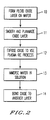
- Wafer 30 preferably a processed semiconductor device wafer and more preferably a processed silicon device wafer, contains a device layer 31 with processed devices.
- Device layer 31 may contain a number of layers and include surface regions of wafer 30. The surface topography of layer 31 is typically nonplanar.
- Layer 31 may also represent a processed integrated circuit containing any number of layers such as active devices, interconnection, insulation, etc.
- the integrated circuit may be fully processed, or partially processed where the remaining processing is performed after the bonding process.
- the processing after the bonding may include full or partial substrate removal or via formation between the bonded wafers for interconnection.
- Bonding layer 32 may be any solid state material or mixed materials which can be deposited or formed at low temperatures and can be polished to a sufficiently smooth surface.
- Layer 32 may be an insulator, such as SiO 2 , silicon nitride, amorphous silicon formed using chemical vapor deposition (CVD) or plasma-enhanced CVD (PECVD), sputtering or by evaporation. Other materials such as polymers, semiconductors or sintered materials may also be used.
- Layer 32 should have thickness greater than the surface topography of layer 31.
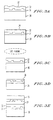
- the surface 33 of layer 32 is planarized and smoothed, as shown in step 2 of FIG. 1 and in FIG. 3B . It is noted that the roughness/planarity of surface 33 is exaggerated in FIG. 3A for illustrative purposes.
- This step may be accomplished using chemical-mechanical polishing.
- Surface 33 is preferably polished to a roughness of about no more than about 3 nm and preferably no more than about 0.1 nm and be substantially planar.
- the surface roughness values are typically given as root-mean square (RMS) values. Also, the surface roughness may be given as mean values which are nearly the same as the RMS values.
- polishing surface 33 is cleaned and dried to remove any residue from the polishing step. Polished surface 33 is preferably then rinsed with a solution.
- the bonding surface may also be etched prior to polishing to improve the planarity and/or surface roughness.
- the etching can be effective to remove high spots on the bonding surface by selective etching of the high spots using, for example, standard photolithographic techniques.
- a layer of silicon nitride can be embedded within a silicon dioxide bonding layer 32 that can serve as an etch stop when using a solution containing HF.
- the etch stop material may be used to improve uniformity, reproducibility, and manufacturability.
- FIG. 3B illustrates layer 32 having upper surface 34 after the polishing/planarization and cleaning steps.
- Surface 34 then undergoes an activation process (step 3, FIG. 1 ).
- This activation process is an etching process and preferably a very slight etch (VSE) process.
- VSE means that the root-mean-square micro-roughness (RMS) of the very slightly etched surface remains at approximately the unetched value, typically ⁇ 0.5 nm and preferably in the range of 0.1 nm to 3 nm.
- RMS root-mean-square micro-roughness
- the optimum amount of material removed depends upon the material and the method used for removal. Typical amounts removed vary from Angstroms to a few nanometers. It is also possible to remove more material.
- VSE also includes the breaking of bonds on the treated surfaces and can occur without significant removal of material.
- the VSE is distinct from simple modification of the surface by, for example, charging the surface with electronic charge or damaging the surface layer.
- the VSE process consists of a gas or mixed gas (such as oxygen, argon, nitrogen, CF 4 , NH 3 ) plasma process at a specified power level for a specified time ( FIG. 3C ).
- the power and duration of the plasma process will vary depending upon the materials used to obtain the desired bond energy. Examples are given below, but in general, the power and duration will be determined empirically.
- the plasma process may be conducted in different modes. Both reactive ion etch (RIE) and plasma modes may be used, as well as an inductively-coupled plasma mode (ICP). Sputtering may also be used. Data and examples are given below in both the RIE and plasma modes.
- RIE reactive ion etch
- ICP inductively-coupled plasma mode
- the VSE process etches the surface very slightly via physical sputtering and/or chemical reaction and preferably is controlled to not degrade the surface roughness of the bonding surfaces.
- the surface roughness may even be improved depending upon the VSE and materials etched. Almost any gas or gas mixture that will not etch surface 34 excessively can be used for the room temperature bonding method according to the invention.
- the VSE serves to clean the surface and break bonds of the oxide on the wafer surface.
- the VSE process can thus enhance the surface activation significantly.
- a desired bonding species can be used to terminated on surface 34 during the VSE by proper design of the VSE.
- a post-VSE treatment that activates and terminates the surface with a desired terminating species during the post-VSE process may be used.
- the desired species further preferably forms a temporary bond to the surface 34 atomic layer, effectively terminating the atomic layer, until a subsequent time that this surface can be brought together with a surface terminated by the same or another bonding species 36 as shown in FIG. 3D .
- Desired species on the surfaces will further preferably react with each other when they are in sufficiently close proximity allowing chemical bonding between surfaces 34 and 36 at low or room temperature that is enhanced by diffusion or dissociation and diffusion of the reacted desired species away from the bonding interface.
- the post-VSE process preferably consists of immersion in a solution containing a selected chemical to generate surface reactions that result in terminating the bonding surface 34 with desired species.
- the immersion is preferably performed immediately after the VSE process.
- the post-VSE process may be performed in the same apparatus in which the VSE process is conducted. This is done most readily if both VSE and post-VSE processes are either dry, i.e, plasma, RIE, ICP, sputtering, etc, or wet, i.e., solution immersion.
- a desired species preferably consists of a monolayer or a few monolayers of atoms or molecules.
- the post-VSE process may also consist of a plasma, RIE, or other dry process whereby appropriate gas chemistries are introduced to result in termination of the surface with the desired species.
- the post-VSE process may also be a second VSE process.
- the termination process may also include a cleaning process where surface contaminants are removed without VSE. In this case, a post-cleaning process similar to the post-VSE processes described above then results in a desired surface termination.
- the post-VSE or post-cleaning process may or may not be needed to terminate surfaces with desired species if the activated surface bonds by the cleaning or VSE process are subsequently sufficiently weakly surface reconstructed and can remain sufficiently clean before bonding such that subsequent bonding with a similar surface can form a chemical bond.
- the wafers are optionally rinsed then dried.
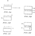
- Two wafers are bonded by aligning them (if necessary) and bringing them together to form a bonding interface.
- a second wafer 35 has been processed in the manner shown in FIG. 3C to prepare bonding surface 36.
- the two wafers are brought together by, for example, commercially available wafer bonding equipment (not shown) to initiate bonding interface 37 ( FIG. 3E ).
- a spontaneous bond then typically occurs at some location in the bonding interface and propagates across the wafer.
- a chemical reaction such as polymerization that results in chemical bonds takes place between species used to terminate surfaces 34 and 36 when the surfaces are in sufficient proximity.
- the bonding energy is defined as the specific surface energy of one of the separated surfaces at the bonding interface that is partially debonded by inserting a wedge.
- the by-products of the reaction then diffuse away from the bonding interface to the wafer edge or are absorbed by the wafers, typically in the surrounding materials.
- the by-products may also be converted to other by-products that diffuse away or are absorbed by the wafers.
- the amount of covalent and/or ionic bonding may be increased by removal of converted species resulting in further increase in bond strength.
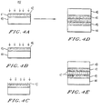
- FIGS. 4A-4E show surface conditions and the bonding propagation to form covalent bonds in a the case of a planar Si wafer covered with silicon oxide.
- Si wafer 40 On Si wafer 40 an SiO 2 layer 41 is formed, which has been polished and planarized. Surface 42 of layer 41 is subjected to the VSE process to produce an activated surface ( FIG. 4A ).
- a second SiO 2 layer 45 is formed, and surface 46 is subjected to a VSE process to activate surface 46 ( FIG. 4B ). Desired species are terminated on surface 46 and are shown as lines 43 in FIG. 4C . Either or both of a VSE and post-VSE processes are used to properly terminate surface 46.
- surface 42 may also be terminated using a post-VSE process.
- Wafer 44 is brought together with wafer 40 ( FIG. 4D ) and bonds 46 begin to form the bonding propagates and by-products are removed (indicated as arrows 47) and chemical bonds (such as covalent) are formed, as shown in FIG. 4E .
- the bonding immediately after the RIE process may use a special bonding fixture allowing immediate in situ bonding of the etched wafers.
- a diagram of the fixture is shown in FIG. 7 .
- plasma chamber 75 are two wafers to be bonded 70 disposed on RF electrodes 76 and 77.
- a plasma is formed in zone 79 by the application of RF power to the electrodes via moveable vacuum RF power feedthrough 74 and by the introduction of an appropriate gas or gas mixture through gas feedthrough 73.
- Element 71 is a vacuum feedthrough for mechanical actuator (not shown) to retract retractable spacer 72.
- Chamber 75 is pumped down to a desired vacuum level via pumps (not shown) and chamber inlet 78.
- the VSE and post-VSE or post-cleaning may be conducted in chamber 75.
- the mechanical spacers 72 are retracted by the mechanical actuator and the wafers 70 are moved into contact with to begin the bonding process.
- the bonded wafers are then moved from the chamber into ambient or into another vacuum chamber (not shown) and stored for a desired period to allow the bonding to propagate by a wafer handling system (not shown).
- the materials of the bonding layers preferably have an open structure so that the by-products of the polymerization reaction can be easily removed.
- the bonding species on the opposing bonding surfaces must be able to react at room temperature to form a strong or chemical bond.
- the bond energy is sufficiently high to virtually eliminate slippage between wafers after subsequent heat treatments associated with a subsequent processing or operation when wafers have different thermal expansion coefficients. Lack of slippage is manifest by a lack of wafer bowing upon inspection after the subsequent processing or operation.
- At least one of the wafers is preferable for at least one of the wafers to be as thin as possible because a thin wafer allows compliance to accommodate a lack of perfect surface planarization and smoothness. Thinning to thickness of about 10 mils to 10 microns is effective.
- the bonded wafers are preferably stored at ambient or at low or room temperature after bonding to allow removal of species or converted species for a specified period of time depending upon the materials and species used. Twenty four hours is usually preferable. The storage time is dependent upon the type of plasma process used. Chemical bonds may be obtained more quickly, in a matter of minutes, when certain plasma processes such as an Ar plasma are used. For example, 585 mJ/m 2 bonds were obtained in immediately after bonding and over 800 mJ/m 2 were observed after 8 hours for deposited oxides etched by an Ar plasma followed by NH 4 OH dip.
- Annealing the bonded wafers during bonding may increase the bonding strength.
- the annealing temperature should be below 200 °C and may be typically in the range of 75-100 °C. Storing the bonded wafers under vacuum may facilitate the removal of residual gasses from the bonding surfaces, but is not always necessary.
- All of the processes above may be carried out at or near room temperature.
- the wafers are bonded with sufficient strength to allow subsequent processing operations (lapping, polishing, substrate removal, chemical etching, lithography, masking, etc.). Bonding energies of approximately 500-2000 mJ/m 2 or more can be achieved (see FIG. 6A ).
- CMOS and bipolar or III-V HBT and Si CMOS complementary metal-oxide-semiconductor
- Other elements or materials such as thermal spreaders, surrogate substrates, antennas, wiring layers, a pre-formed multi-layer interconnects, etc. may be bonded to produce different types of circuits or systems, as desired.
- PECVD SiO 2 is deposited on a Si wafer containing devices.
- Surface 34 after the plasma (such as argon, oxygen or CF 4 ) treatment, is mainly terminated by Si-OH groups due to the availability of moisture in the plasma system and in air.
- the wafers are immediately immersed in solution such as ammonium hydroxide (NH 4 OH), NH 4 F or HF for a period such as between 10 and 120 seconds.
- solution such as ammonium hydroxide (NH 4 OH), NH 4 F or HF
- Si-F groups are terminating on the PECVD SiO 2 surface after an NH 4 F or HF immersion.
- the hydrogen bonded Si-NH2:Si-OH groups or Si-NH2:Si-NH2 groups across the bonding surfaces can polymerize at room temperature in forming Si-O-Si or Si-N-N-Si (or Si-N-Si) covalent bonds:
- the HF or NH 4 F dipped oxide surfaces are terminated by Si-F groups in addition to Si-OH groups. Since HF or NH 4 F solution etches silicon oxide strongly, their concentrations must be controlled to an adequately low level, and the immersion time must be sufficiently short. This is an example of a post-VSE process being a second VSE process.
- the covalent bonds across the bonding interface are formed due to the polymerization reaction between hydrogen bonded Si-HF or Si-OH groups:
- FIG. 8 shows the fluorine concentration profile of bonded thermal oxide covered silicon wafers that were dipped in 0.05% HF before room temperature bonding. A fluorine concentration peak is clearly seen at the bonding interface. This provides evidence of the chemical process described above where the desired species are located at the bonding interface.
- reaction (2) Since reaction (2) is reversible only at relatively high temperatures of ⁇ 500EC, the formed siloxane bonds should not be attacked by NH 3 at lower temperatures. It is known that H 2 molecules are small and diffuse about 50 times quicker than water molecules in oxide. The existence of a damaged layer near the surface of an adequate thickness i.e. a few nm, will facilitate the diffusion or dissolution of NH 3 , and HF and hydrogen in reactions (2), (3), (4) and/or (5) in this layer and enhancement of the chemical bond. The three reactions result in a higher bonding energy of SiO 2 /SiO 2 bonded pairs at room temperature after a period of storage time to allow NH 3 or H 2 to diffuse away.
- the plasma treatment may create a damaged or defective area in the oxide layer near the bonding surface.
- the zone extends for a few monolayers.
- the damaged or defective area aids in the removal of bonding by-products. Efficient removal of the bonding by-products improves the bonding strength since the by-products can interfere with the bonding process by preventing high-strength bond from forming.
- Many different surfaces of materials may be smoothed and/or planarized, followed by a cleaning process, to prepare for bonding according to the invention.
- These materials can be room temperature bonded by mating surfaces with sufficient planarity, surface smoothness, and passivation that includes cleaning, and/or VSE, activation and termination.
- Amorphous and sintered materials, non-planar integrated circuits, and silicon wafers are examples of such materials.
- Single crystalline semiconductor or insulating surfaces, such as SiO 2 or Si surfaces can also be provided with the desired surface roughness, planarity and cleanliness. Keeping the surfaces in high or ultra-high vacuum simplifies obtaining surfaces sufficiently free of contamination and atomic reconstruction to achieve the strong bonding according to the invention.
- semiconductor or insulator materials such as InP, GaAs, SiC, sapphire, etc.
- PECVD SiO 2 may be deposited on many types of materials at low temperatures, many different combinations of materials may be bonded according to the invention at room temperature. Other materials may also be deposited as long as appropriate processes and chemical reactions are available for the VSE, surface activation, and termination.
- the method may also be used with silicon nitride as the bonding material.
- Silicon nitride may be bonded to silicon nitride, or to silicon dioxide and silicon. Silicon oxide may also be bonded to silicon.
- Other types of dielectric materials may be bonded together including aluminum nitride and diamond-like carbon.
- the method may be applied to planar wafers having no devices or circuits and one wafer with devices and circuits.
- the planar wafer may be coated with a bonding layer, such as PECVD oxide or amorphous silicon, and then processed as described above to bond the two wafers.
- the planar wafer may not need to be coated with a bonding layer if it has sufficient smoothness and planarity and the proper bonding material.
- the bonding process may be repeated with any number of wafers, materials or functional elements.
- two device or IC wafers may be joined, followed by removing one of the exposed substrates to transfer a layer or more of devices, or just the active regions of an IC.
- the bonding according to the invention may be applied to joining different types of materials.
- a silicon wafer can be bonded to another silicon wafer, or bond to an oxidized silicon wafer.
- the bare silicon wafer and the oxide covered wafer are immersed in HF, NH 4 F and/or NH 4 OH and bonded after drying.
- the time for the immersion should be less than about twenty minutes for the silicon wafer covered with the thin oxide since the NH 4 OH solution etches silicon oxide. Since HF and NH 4 F etches oxides strongly, very diluted solutions, preferably in 0.01-0.2% range should be used for dipping of the silicon wafers.
- reaction (2), (3), (4) and/or (5) take place at the bonding interface between the two wafers.
- the plasma-treated wafers may also be immersed in deionized water instead of the NH 4 OH solution.
- the silicon bonding may be conducted with a bare silicon wafer, i.e. having a native oxide or a silicon wafer having an oxide layer formed on its surface as described above.
- a bare silicon wafer i.e. having a native oxide or a silicon wafer having an oxide layer formed on its surface as described above.
- the native oxide which if formed on the bare silicon wafer is sputter etched, and the oxide layer formed on the silicon surface is etched.
- the final surface is an activated (native or formed) oxide.
- the activated oxide surface When rinsed in deionized water, the activated oxide surface is mainly terminated with Si-OH groups. Since oxide growth in oxygen plasma has been found to have less water than in normal native oxide layers, the water from the original bonding bridge and generated by the following polymerization reaction (6) can be absorbed into the plasma oxide readily.
- FIGS. 5A-5E illustrate bonding two silicon wafers.
- Wafers 50 and 52 have respective surfaces 51 and 53 with native oxides (not shown) subjected to a VSE process.
- Surface 53 is in FIG. 5C is shown terminated with a desired species 54.
- the two wafers are brought together and bonds 55 begin to form ( FIG. 5D ).
- the bonding propagates and bonding by-products, in this case H 2 gas, are removed.
- the by-products being removed are shown as arrows 56 in FIG. 5E .
- the water can also diffuse through the thin oxide layer on the bare silicon wafer to react with silicon.
- the silicon surface underneath the oxide has a damaged or defective zone, extending for a few monolayers, the water molecules that diffuse through the oxide layer and reach the damaged or defective zone can be converted to hydrogen at room temperature and be removed readily:
- a relatively thick (-5 nm) oxide layer is formed, it will take a long period of time for the water molecules to diffuse through this thick layer.
- a thin oxide layer is left or a too narrow defective zone is formed, water that can reach the silicon surface may not react sufficiently with the silicon and convert to hydrogen. In both cases the bonding energy enhancement will be limited.
- the preferred oxygen plasma treatment thus leaves a minimum plasma oxide thickness (e.g., about 0.1-1.0 nm) and a reasonably thick defective zone (e.g., about 0.1-0.3 nm) on the silicon surface.
- the VSE process uses wet chemicals.
- an InP wafer having a deposited silicon oxide layer, as in the first embodiment, and a device layer are bonded to a AlN substrate having a deposited oxide layer.
- both wafers are cleaned in an standard RCA cleaning solution.
- the wafers are very slightly etched using a dilute HF aqueous solution with an HF concentration preferably in the range of 0.01 to 0.2%. About a few tenths of a nm is removed and the surface smoothness is not degraded as determined by AFM (atomic force microscope) measurements.
- the wafers are spin dried and bonded in ambient air at room temperature.
- the resulting bonding energy has been measured to reach -700 mJ/m 2 after storage in air. After annealing this bonded pair at 75°C the bonding energy of 1500 mJ/m 2 was obtained.
- the bonding energy has been measured to reach silicon bulk fracture energy (about 2500 mJ/m 2 ) after annealing at 100°C. If the wafers are rinsed with deionized water after the HF dip, the bonding energy at 100°C is reduced to 200 mJ/m 2 , that is about one tenth of that obtained without the rinse. This illustrates the preference of F to OH as a terminating species.
- the VSE process consists of 0.1% HF etching followed by 5 min dip in 0.02% HN 4 F solution of thermally oxidized silicon wafers at room temperature after a standard cleaning process. Without rinsing in deionized water, the wafers are bonded after spin drying at room temperature. The bonding energy of the bonded pairs reaches -1700 mJ/m 2 after 100°C annealing. If the wafers are rinsed in de-ionized water after the HF etching before bonding, the bonding energy of bonded pairs is only 400 mJ/m 2 , again illustrating the preference of F to OH as a terminating species.
- Dilute NH 4 F is used in the VSE process to etch silicon oxide covered wafers in a fourth embodiment.
- concentration of the NH 4 F should be below 0.02% to obtain the desired bonding.
- the bonding energy of ⁇ 600 mJ/m 2 can be achieved at room temperature after storage.
- a fifth embodiment of the invention is used to bond Si surfaces having a native oxide of about 1 nm in thickness.
- a VSE process using 5 min etching in 70% HNO 3 + diluted HF (preferably 0.01 to 0.02%) is performed. Wafers are pulled out of the solution vertically with a basically hydrophobic surface. Without rinsing in water, the wafers were bonded at room temperature in air. In this process covalent bonding occurs at room temperature with measured bonding energies typically about 600 mJ/m 2 . This bonding energy is significantly increased to 1300 mJ/m 2 after annealing at 75°C and reaches the fracture energy of bulk silicon (about 2500 mJ/m 2 ) at a temperature of 100°C.
- diluted HNO 3 with water can be used in the solution to achieve similar results.
- the silicon is etched in the dilute HNO 3 VSE process at a rate of 0.1-0.15 nm/min and a new thick oxide 2.5-3.5 nm in thickness is formed.
- the VSE process may consist of a dry etch that has chemical and/or physical components.
- chemical etching may result from SF 4 /H 2 gas mixture while physical etching may result from Ar etch.
- physical etching may result from Ar etch.
- chemical etching may use CF 4 while physical etching may use oxygen or argon gas.
- thermally stable polymer material for the bonding materials and bond two polymer surfaces together. Examples are polyimides or spin-on materials.
- VSE very slight etching
- the oxide covered wafer bonding case is similar except that a different surface termination is preferred.
- the highly reactive surface layers of oxide and silicon to allow water adsorption and conversion to hydrogen should be formed.
- the highly reactive layers can be a plasma thin oxide layer and a damaged silicon surface layer.
- the oxide on the silicon wafer will also have some damage. Not only O 2 plasma but also plasma of other gases (such as Ar, CF 4 ) are adequate.
- VSE silicon surface is readily to react with moisture to form an oxide layer, and the underlying damaged silicon layer is created by VSE. Since the VSE and by-products removal methods are rather general in nature, this approach can be implemented by many means and apply to many materials.
- a first example three inch ⁇ 100>, 1-10 ohm-cm, boron doped silicon wafers were used.
- PECVD oxide was deposited on some of the silicon wafers.
- thermal oxidized silicon wafers were also studied.
- the PECVD oxide thickness was 0.5 ⁇ m and 0.3 ⁇ m on the front side and the back side of the wafers, respectively.
- Oxide is deposited on both sides of the wafer to minimize wafer bow during polishing and improve planarization.
- a soft polish was performed to remove about 30 nm of the oxide and to smooth the front oxide surface originally having a root mean square of the micro-roughness (RMS) of ⁇ 0.56 nm to a final ⁇ 0.18 nm.
- RMS micro-roughness
- a modified RCA1 solution was used to clean the wafer surfaces followed by spin-drying.
- Two wafers were loaded into the plasma system, both wafers are placed on the RF electrode and treated in plasma in RIE mode. For comparison, some wafers were treated in plasma mode in which the wafers were put on the grounded electrode.
- An oxygen plasma was used with a nominal flow rate of 16 scc/m.
- the RF power was 20-400 W (typically 80 W) at 13.56 MHz and the vacuum level was 100 mTorr.
- the oxide covered wafers were treated in plasma for times between 15 seconds to 5 minutes.
- the plasma treated silicon wafers were then dipped in an appropriate solution or rinse with de-ionized water followed by spin-drying and room temperature bonding in air. Some of the plasma treated wafers were also directly bonded in air without rinse or dipping.
- E and tw are the Young's modulus and thickness for wafers one and two and tb is the thickness of a wedge inserted between the two wafers that results in a wafer separation of length L from the edge of the wafers.
- the room temperature bonding energy as a function of storage time of bonded plasma treated oxide covered silicon wafers is shown in FIG. 6A .
- This figure shows measured room temperature bonding energy versus storage time for 4 different cases as shown.
- the results can be summarized as follows: (1) for dipped and bonded RIE plasma treated oxide wafers, the room temperature bonding energy increases with storage time and reaches a stable value after -20 h in air or at low vacuum; (2) RIE mode results in higher bonding energies than plasma mode; (3) too short a plasma exposure time or too low a plasma power provides a small or negligible increase in bond energy; (4) NH 4 OH dip after plasma treatment shows a much higher increase in bonding energy than water rinse; (5) direct bonding in air after plasma treatment without dipping or rinse shows an almost constant bonding energy with time.
- the bonding energy of the directly bonded wafer pairs immediately after room temperature bonding is slightly higher than the de-ionized water rinsed or NH 4 OH dipped wafer pairs.
- FIG. 6B shows room temperature bonding of Si and AlN wafers with PECVD oxide deposited layers. After about 100 h of storage time a bonding energy of over 2000 mJ/m 2 were observed.
- the bonding energy as a function of storage time of O 2 plasma treated thermally oxidized silicon wafer pairs is similar to wafers with PECVD oxide, although the values of the room temperature bonding energy are somewhat lower.
- the bonding energy as high as ⁇ 1000 mJ/m2 was reached in the RIE mode plasma treated and NH 4 OH dipped PECVD oxide covered wafer pairs. Since the maximum bonding energy of a van der Waals bonded silicon oxide covered wafer pairs is about 200 mJ/m 2 , a large portion of the bonding energy is attributed to the formation of covalent bonds at the bonding interface at room temperature according to the above equation.
- the above process was applied to bond processed InP wafers (600 ⁇ m thick) to AlN wafers (380 ⁇ m thick), or to bond processed Si (380 ⁇ m thick) and InP (600 ⁇ m thick) wafers, as second and third examples.
- the processed InP device wafers are covered with PECVD oxide and planarized and smoothed by chemical-mechanical polishing CMP.
- a PECVD oxide layer is also deposited on the AlN wafers and is planarized and smoothed to improve the RMS surface roughness.
- the processed Si and processed InP wafers are deposited with PECVD oxide and planarized and smoothed using CMP. After VSE similar to the example 1 bonding at room temperature, the bonded wafers are left in ambient air at room temperature.
- bonding energy 1000 mJ/m 2 and 1100 mJ/m 2 were achieved for the InP/Si and InP/AlN bonded pairs, respectively.
- bonding energy at room temperature as high as 2500 mJ/m 2 has been achieved.
- These room temperature bonded plasma treated wafer pairs have sufficient bonding strength to sustain subsequent substrate lapping and etching and other typical semiconductor fabrication processes before or after substrate removal.
- the InP substrate in the room temperature bonded InP/AlN pairs was lapped with 1900# Al 2 O 3 powder from initial 600 ⁇ m thick to ⁇ 50 ⁇ m thick followed by etching in an HCl/H3PO4 solution to leave about a 2.0 ⁇ m thick InP device layer on the AlN or Si wafer.
- the water and etching solution did not penetrate into the bonding interface.
- Surfaces are sputter etched by energetic particles such as radicals, ions, photons and electrons in the plasma or RIE mode.
- the O 2 plasma under conditions that bring about the desired VSE is sputter-etching about 2 ⁇ /min of PECVD oxide as measured by a reflectance spectrometry.
- the sputter etching rate is about 0.5 ⁇ /min.
- the thickness of oxide before and after plasma treatment was measured by a reflectance spectrometry and averaged from 98 measured points on each wafer.
- the etching by O 2 plasma has not only cleaned the surface by oxidation and sputtering but also broken bonds of the oxide on the wafer surfaces.
- the surface roughness of plasma treated oxide surfaces must not be degraded by the etching process.
- AFM measurements show that compared with the initial surface roughness, the RMS of the O 2 plasma treated oxide wafers was ⁇ 2 ⁇ and did not change noticeably.
- the bonding energy enhancement effect is also small. Keeping other conditions unchanged when the O 2 plasma treatment was performed with plasma mode rather than RIE mode, the etching of oxide surfaces is negligible and the oxide thickness does not change.
- the fmal room temperature bonding energy is only 385 mJ/m 2 compared to 1000 mJ/m 2 of RIE treated wafers (see FIG. 6A ).
- CF 4 /O 2 RIE was used to remove -4 nm of PECVD oxide from the wafer surfaces prior to bonding.
- the bonding energy of room temperature bonded PECVD oxide covered silicon wafers was also enhanced significantly in this manner and exceeds 1000 mJ/m2 after sufficient storage time (see also FIG. 6A ).
- An argon plasma has also been used for the VSE with a nominal flow rate of 16 scc/m.
- the RF power was typically 60 W at 13.56 MHz and the vacuum level was 100 mTorr.
- the oxide covered silicon wafers were treated in plasma in RIE mode for times between 30 seconds to 2 minutes.
- the plasma treated silicon wafers were then dipped in an NH 4 OH solution followed by spin-drying and room temperature bonding in air. The bonding energy reached -800 mJ/m 2 at room temperature after only 8 h storage in air.
Landscapes
- Engineering & Computer Science (AREA)
- Power Engineering (AREA)
- Microelectronics & Electronic Packaging (AREA)
- Computer Hardware Design (AREA)
- Physics & Mathematics (AREA)
- Condensed Matter Physics & Semiconductors (AREA)
- General Physics & Mathematics (AREA)
- Manufacturing & Machinery (AREA)
- Chemical & Material Sciences (AREA)
- Inorganic Chemistry (AREA)
- Ceramic Engineering (AREA)
- Chemical Kinetics & Catalysis (AREA)
- General Chemical & Material Sciences (AREA)
- Pressure Welding/Diffusion-Bonding (AREA)
- Mechanical Treatment Of Semiconductor (AREA)
- Drying Of Semiconductors (AREA)
- Internal Circuitry In Semiconductor Integrated Circuit Devices (AREA)
- Cleaning Or Drying Semiconductors (AREA)
Abstract
A method for bonding at low or room temperature includes steps of surface cleaning and activation by cleaning or etching. One etching process The method may also include removing by-products of interface polymerization to prevent a reverse polymerization reaction to allow room temperature chemical bonding of materials such as silicon, silicon nitride and SiO2. The surfaces to be bonded are polished to a high degree of smoothness and planarity. VSE may use reactive ion etching or wet etching to slightly etch the surfaces being bonded. The surface roughness and planarity are not degraded and may be enhanced by the VSE process. The etched surfaces may be rinsed in solutions such as ammonium hydroxide or ammonium fluoride to promote the formation of desired bonding species on the surfaces.
Description
- The present invention relates to bonding of materials at room temperature and, in particular, to bonding of processed semiconductor materials, such as integrated circuit or device substrates, having activated surfaces to achieve high bonding strength adequate for subsequent fabrication and/or a desired application.
- Direct room temperature bonding generally produces weak van der Waals or hydrogen bonding. Annealing is typically required to convert the weak bond to a stronger chemical bond such as a covalent bond. Other wafer bonding techniques including anodic and fusion typically require the application of voltage, pressure and/or annealing at elevated temperature to achieve a sufficient bond strength for subsequent fabrication and/or the desired application. The need to apply voltage, pressure or heat has significantly limited wafer bonding applications because these parameters can damage the materials being wafer bonded, give rise to internal stress and introduce undesirable changes in the devices or materials being bonded. Achieving a strong bond at low temperatures is also critical for bonding of thermally mismatched or thermally sensitive wafers including processed device wafers.
- Ultra high vacuum (UHV) bonding is one of the approaches to achieve a low or room temperature strong bond. However, the bonding wafers still have to be pre-annealed at high temperatures, for instance >600°C for silicon and 500°C for GaAs, before cooling down to low or room temperature for bonding. Furthermore, the UHV approach does not generally work on commonly used materials, for example, in SiO2. It is further also expensive and inefficient.
- Adhesive layers can also be used to bond device wafers to a variety of substrates and to transfer device layers at low temperatures. However, thermal and chemical instability, interface bubbles, stress and the inhomogeneous nature of adhesive layers prevent its wide application. It is thus highly desirable to achieve a strong bond at room temperature by bonding wafers in ambient without any adhesive, external pressure or applied electric field.
- Low vacuum bonding has been explored as a more convenient alternative to UHV bonding but a bonding energy comparable to the bulk silicon fracture energy using bonded bare silicon wafer pairs has only be achieved after annealing at ∼150°C. For oxide covered silicon wafer pairs annealing at ∼300° C is required to obtain a high bond energy. It has not been possible to obtain high bonding energies in bonded material using low vacuum bonding at room temperature.
- A gas plasma treatment prior to bonding in ambient is known to enhance the bonding energy of bonded silicon pairs at low or room temperature. See, for example, G.L. Sun, Q.-Y. Tong, et al., J. de Physique, 49(C4), 79 (1988); G.G. Goetz, Proc. of 1st Intl. Symp. on Semicond. Wafer Bonding: Science, Technol. and Applications, The Electrochem. Soc., 92-7, 65 (1992; S. Farrens et al., J. Electroch. Soc., 142,3950 (1995) and Amirffeiz et al, Abstracts of 5th Symp. on Semi. Wafer Bonding: Science, Tech. and Appl., The Electrochemical Society, 99-2, Abstract No. 963 (1999). Although these treatments have increased the bond energy obtainable at low or room temperature, they have only been demonstrated with planar silicon wafers or with silicon wafers using a plasma process that results in oxide being grown on the wafers during the plasma process. Moreover, these treatments have only been used to increase the bond energy by charging or damaging the surface. Furthermore, these treatments have not been used or shown to be applicable to deposited dielectrics or other materials.
- Obtaining low or room temperature bonding with a method that is not only applicable to planar silicon and grown oxide surfaces but further to deposited materials and non-planar surfaces with planarized deposited materials will allow generic materials, including processed semiconductor wafers, to be bonded with minimal damage for manufacturing purposes. Such a method based on etching and chemical bonding is described herein.
- It is an object of the invention to provide a method for bonding materials at low or room temperature.
- It is another object of the invention to bond materials by cleaning and activating the bonding surfaces to promote chemical bond formation at about room temperature.
- It is a further object of the invention to provide a bonding method to bond any solid state material such as processed device or integrated circuit wafers or thermally sensitive or mis-matched materials at or about room temperature.
- It is further object of the invention to provide a bonding method to bond processed device or integrated circuit wafers of different types of devices or different technologies, and transfer a layer of devices or circuits at or about room temperature.
- It is another object of the invention to enable a direct wafer bonding method that does not require annealing to achieve a required bond strength.
- It is a further object of the invention to provide a method whereby diverse materials including those with non-planar surfaces and deposited materials can be planarized and bonded.
- These and other objects are achieved by a method of bonding having steps of forming first and second bonding surfaces, etching the first and second bonding surfaces, and
bonding together at room temperature the first and second bonding surfaces after said etching step. The etching may include etching the first and second bonding surfaces such that respective surface roughnesses of the first and second bonding surfaces after said etching are substantially the same as respective surface roughnesses before said etching. The surface roughness may be in a range of 0.1 to 3.0 nm. - The bonding surfaces may be the surface of a deposited insulating material, such as silicon oxide, silicon nitride or a dielectric polymer. The bonding surface may also be the surface of a silicon wafer. Silicon wafers, using either the surface of the wafer or a deposited material on the wafer, may be bonded together. The wafers may have devices or integrated circuits formed therein. The devices and circuits in the wafers bonded together may be interconnected. The wafers may have a non-planar surface or an irregular surface topology upon which a material is deposited to form the bonding surfaces.
- Forming at least one of the bonding surfaces may include depositing a polishable material on a non-planar surface. Depositing said polishable material may include depositing one of silicon oxide, silicon nitride or a dielectric polymer. The bonding surfaces may be polished using a method such as chemical-mechanical polishing. The surfaces may also be etched prior to the polishing.
- The etching step may also include activating the first and second bonding surfaces and forming selected bonding groups on the first and second bonding surfaces. Bonding groups may also be formed capable of forming chemical bonds at approximately room temperature, and chemical bonds may be formed between the bonding surfaces allowing bonded groups to diffuse or dissociate away from an interface of the bonding surfaces. The chemical bonds can increase the bonding strength between the bonding surfaces by diffusing or dissociating away said bonding groups.
- After said etching step, the bonding surfaces may be immersed in a solution to form bonding surfaces terminated with desired species. The species may comprise at least one of a silanol group, an NH2 group, a fluorine group and an HF group. Also, a monolayer of one of a desired atom and a desired molecule may be formed on the bonding surface. Terminating the surface may include rinsing said bonding materials in an ammonia-based solution after said slightly etching. The ammonia-based solution may be ammonium hydroxide or ammonium fluoride.
- The method may also include exposing the bonding surfaces to one of an oxygen, argon, NH3 and CF4 RIE plasma process. Silicon dioxide may be deposited as to form the bonding surfaces, and etched using the RIE process.
- The etching process may create a defective or damaged zone proximate to the bonding surfaces. The defective or damaged zone can facilitate the removal of bonding by-products through diffusion or dissociation.
- The method may also include steps of forming first and second bonding surfaces, etching the bonding surfaces, terminating the bonding surfaces with a species allowing formation of chemical bonds at about room temperature, and bonding the bonding surfaces at about room temperature, or may include steps of forming the bonding surfaces each having a surface roughness in a range of 0.1 to 3 nm, removing material from the bonding surfaces while maintaining said surface roughness, and directly bonding the bonding surfaces at room temperature with a bonding strength of at least 500 mJ/m2, at least 1000 mJ/m2, or at least 2000 mJ/m2.
- The objects of the invention may also be achieved by a bonded device having a first material having a first etched bonding surface, and a second material having a second etched bonding surface directly bonded to the first bonding surface at room temperature having a bonding strength of at least 500 to 2000 mJ/m2. The bonding surfaces may be being activated and terminated with a desired bonding species, and the desired species may include a monolayer of one of a desired atom and a desired molecule on said bonding surface or at least one of a silanol group, an NH2 group, a fluorine group and an HF group. The bonding surfaces may each have a defective region located proximate to said first and second bonding surfaces, respectively.
- The first material may include a surface of a first semiconductor wafer having devices formed therein, and the second material may include a surface of a second semiconductor wafer having devices formed therein. Devices in the wafers may be interconnected, and the wafers may be of different technologies. The wafers may also have an integrated circuit formed therein, and devices or circuits in the wafers may be interconnected.
- One of said first and second wafers may be a device region after removing a substantial portion of a substrate of said one of said first and second wafers. The wafers may have an irregular surface topology.
- The first material may include a first wafer containing electrical devices and having a first non-planar surface, and the first bonding surface may include a polished and etched deposited oxide layer on said first non-planar surface. The second material may include a second wafer containing electrical devices and having a second non-planar surface, and the second bonding surface may include a polished, planarized and slightly etched deposited oxide layer on the second non-planar surface.
- The first material may include a first wafer containing electrical devices and having a first surface with irregular topology, and the first bonding surface may include a polished, planarized and slightly etched deposited oxide layer on the first surface. The second material may include a second wafer containing electrical devices and having a second surface with irregular topology, and the second bonding surface may include a polished, planarized and slightly etched deposited oxide layer on the second surface.
- The bonded device according to the invention may also include a first material having a first etched and activated bonding surface terminated with a first desired bonding species, and a second material having a second etched and activated bonding surface terminated with a second desired bonding species bonded to the first bonding surface at room temperature.
- A more complete appreciation of the invention and many of the attendant advantages thereof are readily obtained as the same become better understood by reference to the following detailed description when considered in connection with the accompanying drawings, wherein:
-
FIG. 1 is a flow chart of the method according to the invention; -
FIG. 2 is a flow chart of an example of the method according to the invention; -
FIGS. 3A-3E are diagrams illustrating a first embodiment of a method according to the invention; -
FIG. 4 is a diagram illustrating bonding according to the invention using silicon oxide; -
FIG. 5 is a diagram illustrating bonding according to the invention using silicon; -
FIGS. 6A and6B are graphs of room temperature bonding energy versus storage time; -
FIG. 7 is a diagram of a bonding fixture used in the invention; and -
FIG. 8 is a fluorine concentration profile by SIMS (Secondary Ion Mass Spectroscopy) near the bonding interface of deposited oxide covered silicon wafers that were very slight etched by diluted HF before bonding. - Referring to
FIGS. 1 and3A-3E , a first embodiment of the method according to the invention will be described.Wafer 30, preferably a processed semiconductor device wafer and more preferably a processed silicon device wafer, contains adevice layer 31 with processed devices.Device layer 31 may contain a number of layers and include surface regions ofwafer 30. The surface topography oflayer 31 is typically nonplanar.Layer 31 may also represent a processed integrated circuit containing any number of layers such as active devices, interconnection, insulation, etc. - The integrated circuit may be fully processed, or partially processed where the remaining processing is performed after the bonding process. The processing after the bonding may include full or partial substrate removal or via formation between the bonded wafers for interconnection.
- On layer 31 a
bonding layer 32 is formed (step 1,FIG. 1 ).Bonding layer 32 may be any solid state material or mixed materials which can be deposited or formed at low temperatures and can be polished to a sufficiently smooth surface.Layer 32 may be an insulator, such as SiO2, silicon nitride, amorphous silicon formed using chemical vapor deposition (CVD) or plasma-enhanced CVD (PECVD), sputtering or by evaporation. Other materials such as polymers, semiconductors or sintered materials may also be used.Layer 32 should have thickness greater than the surface topography oflayer 31. - The
surface 33 oflayer 32 is planarized and smoothed, as shown instep 2 ofFIG. 1 and inFIG. 3B . It is noted that the roughness/planarity ofsurface 33 is exaggerated inFIG. 3A for illustrative purposes. This step may be accomplished using chemical-mechanical polishing.Surface 33 is preferably polished to a roughness of about no more than about 3 nm and preferably no more than about 0.1 nm and be substantially planar. The surface roughness values are typically given as root-mean square (RMS) values. Also, the surface roughness may be given as mean values which are nearly the same as the RMS values. After polishingsurface 33 is cleaned and dried to remove any residue from the polishing step.Polished surface 33 is preferably then rinsed with a solution. - The bonding surface may also be etched prior to polishing to improve the planarity and/or surface roughness. The etching can be effective to remove high spots on the bonding surface by selective etching of the high spots using, for example, standard photolithographic techniques. For example, a layer of silicon nitride can be embedded within a silicon
dioxide bonding layer 32 that can serve as an etch stop when using a solution containing HF. The etch stop material may be used to improve uniformity, reproducibility, and manufacturability. -
FIG. 3B illustrateslayer 32 havingupper surface 34 after the polishing/planarization and cleaning steps.Surface 34 then undergoes an activation process (step 3,FIG. 1 ). This activation process is an etching process and preferably a very slight etch (VSE) process. The term VSE means that the root-mean-square micro-roughness (RMS) of the very slightly etched surface remains at approximately the unetched value, typically < 0.5 nm and preferably in the range of 0.1 nm to 3 nm. The optimum amount of material removed depends upon the material and the method used for removal. Typical amounts removed vary from Angstroms to a few nanometers. It is also possible to remove more material. VSE also includes the breaking of bonds on the treated surfaces and can occur without significant removal of material. The VSE is distinct from simple modification of the surface by, for example, charging the surface with electronic charge or damaging the surface layer. In a first example of the method according to the invention, the VSE process consists of a gas or mixed gas (such as oxygen, argon, nitrogen, CF4, NH3) plasma process at a specified power level for a specified time (FIG. 3C ). The power and duration of the plasma process will vary depending upon the materials used to obtain the desired bond energy. Examples are given below, but in general, the power and duration will be determined empirically. - The plasma process may be conducted in different modes. Both reactive ion etch (RIE) and plasma modes may be used, as well as an inductively-coupled plasma mode (ICP). Sputtering may also be used. Data and examples are given below in both the RIE and plasma modes.
- The VSE process etches the surface very slightly via physical sputtering and/or chemical reaction and preferably is controlled to not degrade the surface roughness of the bonding surfaces. The surface roughness may even be improved depending upon the VSE and materials etched. Almost any gas or gas mixture that will not etch
surface 34 excessively can be used for the room temperature bonding method according to the invention. - The VSE serves to clean the surface and break bonds of the oxide on the wafer surface. The VSE process can thus enhance the surface activation significantly. A desired bonding species can be used to terminated on
surface 34 during the VSE by proper design of the VSE. Alternatively, a post-VSE treatment that activates and terminates the surface with a desired terminating species during the post-VSE process may be used. - The desired species further preferably forms a temporary bond to the
surface 34 atomic layer, effectively terminating the atomic layer, until a subsequent time that this surface can be brought together with a surface terminated by the same or another bonding species 36 as shown inFIG. 3D . Desired species on the surfaces will further preferably react with each other when they are in sufficiently close proximity allowing chemical bonding betweensurfaces 34 and 36 at low or room temperature that is enhanced by diffusion or dissociation and diffusion of the reacted desired species away from the bonding interface. - The post-VSE process preferably consists of immersion in a solution containing a selected chemical to generate surface reactions that result in terminating the
bonding surface 34 with desired species. The immersion is preferably performed immediately after the VSE process. The post-VSE process may be performed in the same apparatus in which the VSE process is conducted. This is done most readily if both VSE and post-VSE processes are either dry, i.e, plasma, RIE, ICP, sputtering, etc, or wet, i.e., solution immersion. A desired species preferably consists of a monolayer or a few monolayers of atoms or molecules. - The post-VSE process may also consist of a plasma, RIE, or other dry process whereby appropriate gas chemistries are introduced to result in termination of the surface with the desired species. The post-VSE process may also be a second VSE process. The termination process may also include a cleaning process where surface contaminants are removed without VSE. In this case, a post-cleaning process similar to the post-VSE processes described above then results in a desired surface termination.
- The post-VSE or post-cleaning process may or may not be needed to terminate surfaces with desired species if the activated surface bonds by the cleaning or VSE process are subsequently sufficiently weakly surface reconstructed and can remain sufficiently clean before bonding such that subsequent bonding with a similar surface can form a chemical bond.
- The wafers are optionally rinsed then dried. Two wafers are bonded by aligning them (if necessary) and bringing them together to form a bonding interface. As shown in
FIG. 3D , asecond wafer 35 has been processed in the manner shown inFIG. 3C to prepare bonding surface 36. The two wafers are brought together by, for example, commercially available wafer bonding equipment (not shown) to initiate bonding interface 37 (FIG. 3E ). - A spontaneous bond then typically occurs at some location in the bonding interface and propagates across the wafer. As the initial bond begins to propagate, a chemical reaction such as polymerization that results in chemical bonds takes place between species used to terminate
surfaces 34 and 36 when the surfaces are in sufficient proximity. The bonding energy is defined as the specific surface energy of one of the separated surfaces at the bonding interface that is partially debonded by inserting a wedge. The by-products of the reaction then diffuse away from the bonding interface to the wafer edge or are absorbed by the wafers, typically in the surrounding materials. The by-products may also be converted to other by-products that diffuse away or are absorbed by the wafers. The amount of covalent and/or ionic bonding may be increased by removal of converted species resulting in further increase in bond strength. -
FIGS. 4A-4E show surface conditions and the bonding propagation to form covalent bonds in a the case of a planar Si wafer covered with silicon oxide. OnSi wafer 40 an SiO2 layer 41 is formed, which has been polished and planarized.Surface 42 oflayer 41 is subjected to the VSE process to produce an activated surface (FIG. 4A ). On a second wafer 44 a second SiO2 layer 45 is formed, andsurface 46 is subjected to a VSE process to activate surface 46 (FIG. 4B ). Desired species are terminated onsurface 46 and are shown aslines 43 inFIG. 4C . Either or both of a VSE and post-VSE processes are used to properly terminatesurface 46. While not shown,surface 42 may also be terminated using a post-VSE process.Wafer 44 is brought together with wafer 40 (FIG. 4D ) andbonds 46 begin to form the bonding propagates and by-products are removed (indicated as arrows 47) and chemical bonds (such as covalent) are formed, as shown inFIG. 4E . - The bonding immediately after the RIE process may use a special bonding fixture allowing immediate in situ bonding of the etched wafers. A diagram of the fixture is shown in
FIG. 7 . Inplasma chamber 75 are two wafers to be bonded 70 disposed onRF electrodes zone 79 by the application of RF power to the electrodes via moveable vacuumRF power feedthrough 74 and by the introduction of an appropriate gas or gas mixture throughgas feedthrough 73.Element 71 is a vacuum feedthrough for mechanical actuator (not shown) to retractretractable spacer 72.Chamber 75 is pumped down to a desired vacuum level via pumps (not shown) andchamber inlet 78. In the case where a post-VSE process or post cleaning process is also a dry process, as discussed above, the VSE and post-VSE or post-cleaning may be conducted inchamber 75. - After the plasma treatment to conduct the VSE process, the
mechanical spacers 72 are retracted by the mechanical actuator and thewafers 70 are moved into contact with to begin the bonding process. The bonded wafers are then moved from the chamber into ambient or into another vacuum chamber (not shown) and stored for a desired period to allow the bonding to propagate by a wafer handling system (not shown). - The materials of the bonding layers preferably have an open structure so that the by-products of the polymerization reaction can be easily removed. The bonding species on the opposing bonding surfaces must be able to react at room temperature to form a strong or chemical bond. The bond energy is sufficiently high to virtually eliminate slippage between wafers after subsequent heat treatments associated with a subsequent processing or operation when wafers have different thermal expansion coefficients. Lack of slippage is manifest by a lack of wafer bowing upon inspection after the subsequent processing or operation.
- In order to achieve the high bonding energies, it is preferable for at least one of the wafers to be as thin as possible because a thin wafer allows compliance to accommodate a lack of perfect surface planarization and smoothness. Thinning to thickness of about 10 mils to 10 microns is effective.
- The bonded wafers are preferably stored at ambient or at low or room temperature after bonding to allow removal of species or converted species for a specified period of time depending upon the materials and species used. Twenty four hours is usually preferable. The storage time is dependent upon the type of plasma process used. Chemical bonds may be obtained more quickly, in a matter of minutes, when certain plasma processes such as an Ar plasma are used. For example, 585 mJ/m2 bonds were obtained in immediately after bonding and over 800 mJ/m2 were observed after 8 hours for deposited oxides etched by an Ar plasma followed by NH4OH dip.
- Annealing the bonded wafers during bonding may increase the bonding strength. The annealing temperature should be below 200 °C and may be typically in the range of 75-100 °C. Storing the bonded wafers under vacuum may facilitate the removal of residual gasses from the bonding surfaces, but is not always necessary.
- All of the processes above may be carried out at or near room temperature. The wafers are bonded with sufficient strength to allow subsequent processing operations (lapping, polishing, substrate removal, chemical etching, lithography, masking, etc.). Bonding energies of approximately 500-2000 mJ/m2 or more can be achieved (see
FIG. 6A ). - At this point (
FIG. 3E ) it is possible to remove a part or all of the substrate ofwafer 35 by, for instance, lapping and etch back. The layer of devices ofwafer 35 is thus transferred ontowafer 30. The devices from the two layers may be interconnected. Additional device or circuit layers may be bonded and interconnected to form a multilayer structure. Different types of wafers, devices or circuits may be bonded, as well as different technologies (i.e. CMOS and bipolar or III-V HBT and Si CMOS). Other elements or materials such as thermal spreaders, surrogate substrates, antennas, wiring layers, a pre-formed multi-layer interconnects, etc. may be bonded to produce different types of circuits or systems, as desired. - In anexample, shown in
FIG.2 , PECVD SiO2 is deposited on a Si wafer containing devices.Surface 34, after the plasma (such as argon, oxygen or CF4) treatment, is mainly terminated by Si-OH groups due to the availability of moisture in the plasma system and in air. After the plasma treatment, the wafers are immediately immersed in solution such as ammonium hydroxide (NH4OH), NH4F or HF for a period such as between 10 and 120 seconds. After immersing the wafers in the NH4OH solution, many Si-OH groups are replaced by Si-NH2 groups according to the following substitution reaction:
- Alternatively, many Si-F groups are terminating on the PECVD SiO2 surface after an NH4F or HF immersion.
- The hydrogen bonded Si-NH2:Si-OH groups or Si-NH2:Si-NH2 groups across the bonding surfaces can polymerize at room temperature in forming Si-O-Si or Si-N-N-Si (or Si-N-Si) covalent bonds:


- Alternatively, the HF or NH4F dipped oxide surfaces are terminated by Si-F groups in addition to Si-OH groups. Since HF or NH4F solution etches silicon oxide strongly, their concentrations must be controlled to an adequately low level, and the immersion time must be sufficiently short. This is an example of a post-VSE process being a second VSE process. The covalent bonds across the bonding interface are formed due to the polymerization reaction between hydrogen bonded Si-HF or Si-OH groups:


-
FIG. 8 shows the fluorine concentration profile of bonded thermal oxide covered silicon wafers that were dipped in 0.05% HF before room temperature bonding. A fluorine concentration peak is clearly seen at the bonding interface. This provides evidence of the chemical process described above where the desired species are located at the bonding interface. - Since reaction (2) is reversible only at relatively high temperatures of∼500EC, the formed siloxane bonds should not be attacked by NH3 at lower temperatures. It is known that H2 molecules are small and diffuse about 50 times quicker than water molecules in oxide. The existence of a damaged layer near the surface of an adequate thickness i.e. a few nm, will facilitate the diffusion or dissolution of NH3, and HF and hydrogen in reactions (2), (3), (4) and/or (5) in this layer and enhancement of the chemical bond. The three reactions result in a higher bonding energy of SiO2/SiO2 bonded pairs at room temperature after a period of storage time to allow NH3 or H2 to diffuse away.
- In the example of
FIG. 2 , the plasma treatment may create a damaged or defective area in the oxide layer near the bonding surface. The zone extends for a few monolayers. The damaged or defective area aids in the removal of bonding by-products. Efficient removal of the bonding by-products improves the bonding strength since the by-products can interfere with the bonding process by preventing high-strength bond from forming. - Many different surfaces of materials may be smoothed and/or planarized, followed by a cleaning process, to prepare for bonding according to the invention. These materials can be room temperature bonded by mating surfaces with sufficient planarity, surface smoothness, and passivation that includes cleaning, and/or VSE, activation and termination. Amorphous and sintered materials, non-planar integrated circuits, and silicon wafers are examples of such materials. Single crystalline semiconductor or insulating surfaces, such as SiO2 or Si surfaces, can also be provided with the desired surface roughness, planarity and cleanliness. Keeping the surfaces in high or ultra-high vacuum simplifies obtaining surfaces sufficiently free of contamination and atomic reconstruction to achieve the strong bonding according to the invention. Other semiconductor or insulator materials such as InP, GaAs, SiC, sapphire, etc., may also be used. Also, since PECVD SiO2 may be deposited on many types of materials at low temperatures, many different combinations of materials may be bonded according to the invention at room temperature. Other materials may also be deposited as long as appropriate processes and chemical reactions are available for the VSE, surface activation, and termination.
- For example, the method may also be used with silicon nitride as the bonding material. Silicon nitride may be bonded to silicon nitride, or to silicon dioxide and silicon. Silicon oxide may also be bonded to silicon. Other types of dielectric materials may be bonded together including aluminum nitride and diamond-like carbon.
- The method may be applied to planar wafers having no devices or circuits and one wafer with devices and circuits. The planar wafer may be coated with a bonding layer, such as PECVD oxide or amorphous silicon, and then processed as described above to bond the two wafers. The planar wafer may not need to be coated with a bonding layer if it has sufficient smoothness and planarity and the proper bonding material.
- As can be appreciated, the bonding process may be repeated with any number of wafers, materials or functional elements. For example, two device or IC wafers may be joined, followed by removing one of the exposed substrates to transfer a layer or more of devices, or just the active regions of an IC.
- The bonding according to the invention may be applied to joining different types of materials. For example, a silicon wafer can be bonded to another silicon wafer, or bond to an oxidized silicon wafer. The bare silicon wafer and the oxide covered wafer are immersed in HF, NH4F and/or NH4OH and bonded after drying. The time for the immersion should be less than about twenty minutes for the silicon wafer covered with the thin oxide since the NH4OH solution etches silicon oxide. Since HF and NH4F etches oxides strongly, very diluted solutions, preferably in 0.01-0.2% range should be used for dipping of the silicon wafers.
- After drying the silicon wafer and the oxide-covered wafer are bonded in ambient at room temperature. Reactions (2), (3), (4) and/or (5) take place at the bonding interface between the two wafers. The plasma-treated wafers may also be immersed in deionized water instead of the NH4OH solution.
- The silicon bonding may be conducted with a bare silicon wafer, i.e. having a native oxide or a silicon wafer having an oxide layer formed on its surface as described above. During the oxygen plasma treatment, the native oxide which if formed on the bare silicon wafer is sputter etched, and the oxide layer formed on the silicon surface is etched. The final surface is an activated (native or formed) oxide. When rinsed in deionized water, the activated oxide surface is mainly terminated with Si-OH groups. Since oxide growth in oxygen plasma has been found to have less water than in normal native oxide layers, the water from the original bonding bridge and generated by the following polymerization reaction (6) can be absorbed into the plasma oxide readily.

-
FIGS. 5A-5E illustrate bonding two silicon wafers.Wafers respective surfaces Surface 53 is inFIG. 5C is shown terminated with a desiredspecies 54. The two wafers are brought together andbonds 55 begin to form (FIG. 5D ). The bonding propagates and bonding by-products, in this case H2 gas, are removed. The by-products being removed are shown asarrows 56 inFIG. 5E . - In addition to removal of the water from the bonding interface by dissolving into the plasma activated oxide of the oxidized silicon wafer, the water can also diffuse through the thin oxide layer on the bare silicon wafer to react with silicon. As the silicon surface underneath the oxide has a damaged or defective zone, extending for a few monolayers, the water molecules that diffuse through the oxide layer and reach the damaged or defective zone can be converted to hydrogen at room temperature and be removed readily:

- The reverse reaction of (6) is thus avoided and the room temperature bonding energy increases enormously due to the formation of covalent Si-O-Si bonds.
- If a relatively thick (-5 nm) oxide layer is formed, it will take a long period of time for the water molecules to diffuse through this thick layer. On the other hand, if after the plasma treatment a thin oxide layer is left or a too narrow defective zone is formed, water that can reach the silicon surface may not react sufficiently with the silicon and convert to hydrogen. In both cases the bonding energy enhancement will be limited. The preferred oxygen plasma treatment thus leaves a minimum plasma oxide thickness (e.g., about 0.1-1.0 nm) and a reasonably thick defective zone (e.g., about 0.1-0.3 nm) on the silicon surface.
- In a second embodiment, the VSE process uses wet chemicals. For example, an InP wafer having a deposited silicon oxide layer, as in the first embodiment, and a device layer are bonded to a AlN substrate having a deposited oxide layer. After smoothing and planarizing the InP wafer bonding surface and the AlN wafer bonding surface, both wafers are cleaned in an standard RCA cleaning solution. The wafers are very slightly etched using a dilute HF aqueous solution with an HF concentration preferably in the range of 0.01 to 0.2%. About a few tenths of a nm is removed and the surface smoothness is not degraded as determined by AFM (atomic force microscope) measurements. Without deionized water rinse, the wafers are spin dried and bonded in ambient air at room temperature. The resulting bonding energy has been measured to reach -700 mJ/m2 after storage in air. After annealing this bonded pair at 75°C the bonding energy of 1500 mJ/m2 was obtained. The bonding energy has been measured to reach silicon bulk fracture energy (about 2500 mJ/m2) after annealing at 100°C. If the wafers are rinsed with deionized water after the HF dip, the bonding energy at 100°C is reduced to 200 mJ/m2 , that is about one tenth of that obtained without the rinse. This illustrates the preference of F to OH as a terminating species.
- In a third embodiment the VSE process consists of 0.1% HF etching followed by 5 min dip in 0.02% HN4F solution of thermally oxidized silicon wafers at room temperature after a standard cleaning process. Without rinsing in deionized water, the wafers are bonded after spin drying at room temperature. The bonding energy of the bonded pairs reaches -1700 mJ/m2 after 100°C annealing. If the wafers are rinsed in de-ionized water after the HF etching before bonding, the bonding energy of bonded pairs is only 400 mJ/m2, again illustrating the preference of F to OH as a terminating species.
- Dilute NH4F is used in the VSE process to etch silicon oxide covered wafers in a fourth embodiment. The concentration of the NH4F should be below 0.02% to obtain the desired bonding. The bonding energy of ∼600 mJ/m2 can be achieved at room temperature after storage.
- A fifth embodiment of the invention is used to bond Si surfaces having a native oxide of about 1 nm in thickness. In the fifth embodiment, after cleaning the Si surface by a standard RCA1 cleaning process, a VSE process using 5 min etching in 70% HNO3 + diluted HF (preferably 0.01 to 0.02%) is performed. Wafers are pulled out of the solution vertically with a basically hydrophobic surface. Without rinsing in water, the wafers were bonded at room temperature in air. In this process covalent bonding occurs at room temperature with measured bonding energies typically about 600 mJ/m2. This bonding energy is significantly increased to 1300 mJ/m2 after annealing at 75°C and reaches the fracture energy of bulk silicon (about 2500 mJ/m2) at a temperature of 100°C.
- Instead of 70% HNO3, diluted HNO3 with water can be used in the solution to achieve similar results. According to AMF measurements and high resolution transmission electron microscopy measurement results, the silicon is etched in the dilute HNO3 VSE process at a rate of 0.1-0.15 nm/min and a new thick oxide 2.5-3.5 nm in thickness is formed.
- As further embodiments, the VSE process may consist of a dry etch that has chemical and/or physical components. For a bare Si surface, chemical etching may result from SF4/H2 gas mixture while physical etching may result from Ar etch. For a silicon oxide surface, chemical etching may use CF4 while physical etching may use oxygen or argon gas. It is also possible to use a thermally stable polymer material for the bonding materials and bond two polymer surfaces together. Examples are polyimides or spin-on materials.
- The mechanisms governing the increased bond energy at low or room temperature are similar. A very slight etching (VSE) of the bonding wafers by plasma to clean and activate the surfaces, and improve removal of by-products of interface polymerization to prevent the undesirable reverse reaction and rinse in appropriate solution to terminate the surface with desired species to facilitate room temperature covalent bonding. The oxide covered wafer bonding case is similar except that a different surface termination is preferred. In bare silicon wafer bonding, the highly reactive surface layers of oxide and silicon to allow water adsorption and conversion to hydrogen should be formed. The highly reactive layers can be a plasma thin oxide layer and a damaged silicon surface layer. The oxide on the silicon wafer will also have some damage. Not only O2 plasma but also plasma of other gases (such as Ar, CF4) are adequate. Because during and after VSE the silicon surface is readily to react with moisture to form an oxide layer, and the underlying damaged silicon layer is created by VSE. Since the VSE and by-products removal methods are rather general in nature, this approach can be implemented by many means and apply to many materials.
- In a first example, three inch <100>, 1-10 ohm-cm, boron doped silicon wafers were used. PECVD oxide was deposited on some of the silicon wafers. For comparison, thermal oxidized silicon wafers were also studied. The PECVD oxide thickness was 0.5 µm and 0.3 µm on the front side and the back side of the wafers, respectively. Oxide is deposited on both sides of the wafer to minimize wafer bow during polishing and improve planarization. A soft polish was performed to remove about 30 nm of the oxide and to smooth the front oxide surface originally having a root mean square of the micro-roughness (RMS) of ∼0.56 nm to a final ∼0.18 nm. A modified RCA1 solution was used to clean the wafer surfaces followed by spin-drying.
- Two wafers were loaded into the plasma system, both wafers are placed on the RF electrode and treated in plasma in RIE mode. For comparison, some wafers were treated in plasma mode in which the wafers were put on the grounded electrode. An oxygen plasma was used with a nominal flow rate of 16 scc/m. The RF power was 20-400 W (typically 80 W) at 13.56 MHz and the vacuum level was 100 mTorr. The oxide covered wafers were treated in plasma for times between 15 seconds to 5 minutes. The plasma treated silicon wafers were then dipped in an appropriate solution or rinse with de-ionized water followed by spin-drying and room temperature bonding in air. Some of the plasma treated wafers were also directly bonded in air without rinse or dipping.
- The bonding energy was measured by inserting a wedge into the interface to measure the crack length according to the equation:

- E and tw are the Young's modulus and thickness for wafers one and two and tb is the thickness of a wedge inserted between the two wafers that results in a wafer separation of length L from the edge of the wafers.
- The room temperature bonding energy as a function of storage time of bonded plasma treated oxide covered silicon wafers is shown in
FIG. 6A . This figure shows measured room temperature bonding energy versus storage time for 4 different cases as shown. The results can be summarized as follows: (1) for dipped and bonded RIE plasma treated oxide wafers, the room temperature bonding energy increases with storage time and reaches a stable value after -20 h in air or at low vacuum; (2) RIE mode results in higher bonding energies than plasma mode; (3) too short a plasma exposure time or too low a plasma power provides a small or negligible increase in bond energy; (4) NH4OH dip after plasma treatment shows a much higher increase in bonding energy than water rinse; (5) direct bonding in air after plasma treatment without dipping or rinse shows an almost constant bonding energy with time. The bonding energy of the directly bonded wafer pairs immediately after room temperature bonding is slightly higher than the de-ionized water rinsed or NH4OH dipped wafer pairs. -
FIG. 6B shows room temperature bonding of Si and AlN wafers with PECVD oxide deposited layers. After about 100 h of storage time a bonding energy of over 2000 mJ/m2 were observed. - Comparing different bonding materials, the bonding energy as a function of storage time of O2 plasma treated thermally oxidized silicon wafer pairs is similar to wafers with PECVD oxide, although the values of the room temperature bonding energy are somewhat lower.
- After ∼24 h storage in air at room temperature, the bonding energy as high as ∼1000 mJ/m2 was reached in the RIE mode plasma treated and NH4OH dipped PECVD oxide covered wafer pairs. Since the maximum bonding energy of a van der Waals bonded silicon oxide covered wafer pairs is about 200 mJ/m2, a large portion of the bonding energy is attributed to the formation of covalent bonds at the bonding interface at room temperature according to the above equation.
- The above process was applied to bond processed InP wafers (600 µm thick) to AlN wafers (380 µm thick), or to bond processed Si (380 µm thick) and InP (600 µm thick) wafers, as second and third examples. The processed InP device wafers are covered with PECVD oxide and planarized and smoothed by chemical-mechanical polishing CMP. A PECVD oxide layer is also deposited on the AlN wafers and is planarized and smoothed to improve the RMS surface roughness. The processed Si and processed InP wafers are deposited with PECVD oxide and planarized and smoothed using CMP. After VSE similar to the example 1 bonding at room temperature, the bonded wafers are left in ambient air at room temperature.
- After 24 hours storage at room temperature, bonding energy of 1000 mJ/m2 and 1100 mJ/m2 were achieved for the InP/Si and InP/AlN bonded pairs, respectively. For processed Si (380 µm thick) /oxide covered AlN (280 µm thick) wafer pairs, the bonding energy at room temperature as high as 2500 mJ/m2 has been achieved. These room temperature bonded plasma treated wafer pairs have sufficient bonding strength to sustain subsequent substrate lapping and etching and other typical semiconductor fabrication processes before or after substrate removal.
- The InP substrate in the room temperature bonded InP/AlN pairs was lapped with 1900# Al2O3 powder from initial 600 µm thick to ∼50 µm thick followed by etching in an HCl/H3PO4 solution to leave about a 2.0 µm thick InP device layer on the AlN or Si wafer. The water and etching solution did not penetrate into the bonding interface.
- Surfaces are sputter etched by energetic particles such as radicals, ions, photons and electrons in the plasma or RIE mode. For example, the O2 plasma under conditions that bring about the desired VSE is sputter-etching about 2 Å /min of PECVD oxide as measured by a reflectance spectrometry. For thermal oxide the sputter etching rate is about 0.5 Å/min. The thickness of oxide before and after plasma treatment was measured by a reflectance spectrometry and averaged from 98 measured points on each wafer. The etching by O2 plasma has not only cleaned the surface by oxidation and sputtering but also broken bonds of the oxide on the wafer surfaces.
- However, the surface roughness of plasma treated oxide surfaces must not be degraded by the etching process. AFM measurements show that compared with the initial surface roughness, the RMS of the O2 plasma treated oxide wafers was ∼2 Å and did not change noticeably. On the other hand, if the etching is not sufficiently strong, the bonding energy enhancement effect is also small. Keeping other conditions unchanged when the O2 plasma treatment was performed with plasma mode rather than RIE mode, the etching of oxide surfaces is negligible and the oxide thickness does not change. The fmal room temperature bonding energy is only 385 mJ/m2 compared to 1000 mJ/m2 of RIE treated wafers (see
FIG. 6A ). - Other gas plasma has shown a similar effect. CF4/O2 RIE was used to remove -4 nm of PECVD oxide from the wafer surfaces prior to bonding. The bonding energy of room temperature bonded PECVD oxide covered silicon wafers was also enhanced significantly in this manner and exceeds 1000 mJ/m2 after sufficient storage time (see also
FIG. 6A ). - An argon plasma has also been used for the VSE with a nominal flow rate of 16 scc/m. The RF power was typically 60 W at 13.56 MHz and the vacuum level was 100 mTorr. The oxide covered silicon wafers were treated in plasma in RIE mode for times between 30 seconds to 2 minutes. The plasma treated silicon wafers were then dipped in an NH4OH solution followed by spin-drying and room temperature bonding in air. The bonding energy reached -800 mJ/m2 at room temperature after only 8 h storage in air.
- Obviously, numerous modifications and variations of the present invention are possible in light of the above teachings. It is therefore to be understood that within the scope of the appended claims, the invention may be practiced otherwise than as specifically described herein.
- In particular, the present invention concerns subject matter as defined in the following items:
- 1. A bonding method, comprising: forming first and second bonding surfaces; etching said first and second bonding surfaces; and bonding together at room temperature said first and second bonding surfaces after said etching step.
- 2. A method as recited in
item 1, wherein said etching step comprises: etching said first and second bonding surfaces such that respective surface roughnesses of said first and second bonding surfaces after said etching are substantially the same as respective surface roughnesses before said etching. - 3. A method as recited in
item 2, comprising: forming said first and second bonding surfaces to have a surface roughness in a range of 0. 1 to 3. 0 nm. - 4. A method as recited in
item 1, wherein said etching step comprises: activating said first and second bonding surfaces and forming selected bonding groups on said first and second bonding surfaces. - 5. A method as recited in
item 4, comprising: forming bonding groups capable of forming chemical bonds at approximately room temperature. - 6. A method as recited in
item 1, comprising: forming chemical bonds between said bonding surfaces allowing bonded groups to diffuse or dissociate away from an interface of said first and second bonding surfaces. - 7. A method as recited in item 6, comprising: increasing bonding strength between said first and second bonding surfaces by diffusing or dissociating away said bonding groups.
- 8. A method as recited in
item 1, wherein said etching step comprises: forming a monolayer of one of a desired atom and a desired molecule on said bonding surface. - 9. A method as recited in item 8, wherein said etching step comprises: forming a few monolayers of one of a desired atom and a desired molecule on said bonding surface.
- 10. A method as recited in
item 1, comprising: after said etching step, immersing said first and second bonding surfaces in a solution to form bonding surfaces terminated with desired species. - 11. A method as recited in
item 10, wherein said species comprise at least one of a silanol group, an NH2 group, a fluorine group and an HF group. - 12. A method as recited in
item 10, wherein said etching step comprises: forming a monolayer of one of a desired atom and a desired molecule on said bonding surface. - 13. A method as recited in
item 1, wherein said etching comprises: exposing said first and second bonding surfaces to a plasma. - 14. A method as recited in
item 1, comprising: exposing said first and second bonding surfaces to one of an oxygen, argon, NH3 and
CF4 plasma process. - 15. A method as recited in
item 14, comprising: conducting said plasma process in one of RIE mode, ICP mode, plasma mode and sputtering mode. - 16. A method as recited in
item 1, comprising: polishing respective first and second bonding surfaces to respective desired surface roughnesses and planarity; and etching said first and second bonding surfaces after said polishing to activate said first and second bonding surfaces. - 17. A method as recited in
item 16, wherein: forming at least one of said first and second bonding surfaces comprises depositing a polishable material on a non-planar surface. - 18. A method as recited in
item 17, wherein depositing said polishable material comprises depositing one of silicon oxide, silicon nitride or a dielectric polymer. - 19. A method as recited in
item 1, wherein said etching step comprises: increasing available bonding energy of bonding pairs on said first and second bonding surfaces at approximately room temperature. - 20. A method as recited in
item 19, comprising: obtaining a bond of at least 500 mJ/m2. - 21. A method as recited in
item 19, comprising: obtaining a bond of at least 1000 mJ/m2. - 22. A method as recited in
item 19, comprising: obtaining a bond of at least 2000 mJ/m2. - 23. A method as recited in
item 1, comprising: forming a bond of at least 500 mJ/m2. - 24. A method as recited in
item 1, comprising: obtaining a bond of at least 1000 mJ/m2. - 25. A method as recited in
item 1, comprising: obtaining a bond of at least 2000 mJ/m2. - 26. A method as recited in
item 1, comprising: forming chemical bonds between said bonding surfaces. - 27. A method as recited in item 26, comprising: forming chemical bonds between said bonding surfaces in one of ambient and vacuum.
- 28. A method as recited in item 26, comprising: forming chemical bonds between said bonding surfaces in one of low and ultra high and vacuum.
- 29. A method as recited in
item 1, comprising: forming a bond of sufficient energy to virtually eliminate wafer bowing during subsequent processing of said bonded bonding surfaces. - 30. A method as recited in item 29, comprising: forming a bond of sufficient energy to virtually eliminate wafer bowing during subsequent thermal cycling of said bonded bonding surfaces.
- 31. A method as recited in
item 1, wherein said etching step comprises: increasing available bonding energy of bonding pairs on said first and second bonding surfaces at approximately room temperature; and propagating said bonding at room temperature. - 32. A method as recited in
item 31, comprising: propagating chemical bonding at room temperature. - 33. A method as recited in
item 1, comprising: depositing silicon dioxide as first and second bonding materials having said first and second bonding surfaces; and etching said first and second bonding surfaces using an oxygen plasma. - 34. A method as recited in
item 33, comprising: rinsing said bonding materials in an ammonia-based solution after said etching. - 35. A method as recited in
item 34, comprising: rinsing said bonding materials in ammonium hydroxide after said etching. - 36. A method as recited in
item 34, comprising: rinsing said bonding materials in ammonium fluoride after said etching. - 37. A method as recited in
item 1, comprising: etching said first and second bonding surfaces under vacuum; and bonding said first and second bonding surfaces without breaking said vacuum. - 38. A method as recited in
item 1, comprising: depositing a bonding material on each of first and second surfaces to obtain said first and second bonding surfaces. - 39. A method as recited in item 38, comprising: depositing one of silicon dioxide and silicon nitride as said bonding material.
- 40. A method as recited in
item 1, comprising: depositing silicon dioxide as said bonding material; etching said silicon dioxide using one of oxygen, CF4, and Ar plasma RIE; and rinsing said silicon dioxide in an ammonia-based solution after said etching. - 41. A method as recited in
item 1, comprising: etching said first and second bonding materials using a wet etch process. - 42. A method as recited in
item 42, comprising: immersing said first and second bonding surfaces into a solution after said etching. - 43. A method as recited in
item 1, comprising: depositing silicon dioxide as said bonding material; etching said silicon dioxide using one of diluted HF and diluted NH4F. - 44. A method as recited in
item 43, comprising: rinsing said silicon dioxide in an ammonia-based solution after said etching. - 45. A method as recited in
item 1, comprising: forming said first and second bonding surfaces as silicon and etching said bonding surfaces using a solution of HN03 and diluted HF. - 46. A method as recited in
item 1, comprising: forming said first and second bonding surfaces as silicon each having a native oxide layer ; and activating said native oxide layer using said etching step. - 47. A method as recited in
item 1, comprising: forming said first and second bonding surfaces each as silicon having a native oxide layer; and exposing said first and second bonding surfaces to an oxygen plasma to etch said native oxide layers. - 48. A method as recited in
item 47, creating a defective zone in said silicon during plasma etching. - 49. A method as recited in
item 1, comprising: etching said first and second bonding materials using a plasma RIE process; forming a region having defects proximate to said bonding surface; and removing bonding by-products using said region. - 50. A method as recited in
item 1, wherein said etching comprises: activating said first and second bonding surfaces; and creating a region under said first and second bonding surfaces for removing bonding by-products. - 51. A method as recited in
item 1, comprising: creating a region proximate to said first and second bonding surfaces for at least one of removal and conversion of bonding by-products to a species capable of being absorbed by or diffusing away from said bonding surfaces. - 52. A method as recited in
item 1, comprising: forming said first bonding surface by depositing an oxide layer on a first semiconductor wafer; forming said second bonding surface by depositing an oxide layer on a second semiconductor wafer; and bonding said first and second semiconductor wafers. - 53. A method as recited in
item 1, comprising: forming said first bonding surface as a deposited oxide layer on a first semiconductor wafer, said first wafer comprising a first substrate and a first active region; forming said second bonding surface as a deposited oxide layer on a second semiconductor wafer, said second wafer comprising a second substrate and a second active region ; bonding said first and second semiconductor wafers; and removing at least a substantial portion of one of said first and second substrates after said bonding. - 54. A method as recited in
item 1, comprising: forming said first bonding surface as a deposited oxide layer on a semiconductor wafer, said wafer comprising a substrate and an active region; forming said second bonding surface as a surrogate substrate; bonding said wafer and said surrogate substrate; and removing at least a substantial portion of said first substrate after said bonding. - 55. A method as recited in
item 1, wherein said bonding comprises: maintaining contact between said first and second bonding surfaces for a specified period to produce bonding polymerization and allow removal of by-products. - 56. A method as recited in
item 55, comprising: maintaining said contact between said first and second bonding surfaces for a period less than about 20 hours. - 57. A method as recited in
item 1, wherein said bonding comprises: maintaining said first and second bonding surfaces for a specified period in ambient to remove bonding by-products. - 58. A method as recited in
item 1, comprising: etching said first and second bonding surfaces using a bonding fixture under vacuum ; bonding said first and second bonding surfaces using said fixture to bring together said first and second bonding surfaces while maintaining said vacuum. - 59. A method as recited in
item 1, comprising: forming a first oxide layer on a first wafer containing electrical devices; and polishing said first oxide layer to form said first bonding surface. - 60. A method as recited in item 59, comprising: forming a second oxide layer on a second wafer containing electrical devices; and polishing said second oxide layer to form said second bonding surface.
- 61. A method as recited in
item 60, comprising: forming said first oxide layer on said first wafer containing electrical devices of a first technology; and forming said second oxide layer on said second wafer containing electrical devices of a second technology different from said first technology. - 62. A method as recited in
item 60, comprising: interconnecting said first and second devices. - 63. A method as recited in
item 60, comprising: forming said first bonding surface on a surface of a one of a thermal spreader, surrogate substrate, antenna, wiring layer, and pre-formed multi-layer interconnect. - 64. A method as recited in
item 60, comprising: forming said second bonding surface on a surface of a one of a thermal spreader, surrogate substrate, antenna, wiring layer, and pre-formed multi-layer interconnect. - 65. A method as recited in
item 1, comprising: forming said first bonding surface on a first wafer containing a first integrated circuit. - 66. A method as recited in item 65, comprising: forming said second bonding surface on a second wafer containing a second integrated circuit.
- 67. A method as recited in item 66, comprising: forming said first bonding surface on said first wafer containing said first integrated circuit of a first technology; and forming said second bonding surface on said second wafer containing said second integrated circuit of a second technology different from said first technology.
- 68. A method as recited in item 66, comprising: interconnecting said first and second integrated circuits.
- 69. A method as recited in
item 1, comprising: said first and second bonding surfaces being substantially planar. - 70. A method as recited in
item 1, wherein: forming said first and second bonding surfaces comprises depositing a dielectric material. - 71. A method as recited in
item 70, comprising: polishing said dielectric material to a desired planarity and surface roughness. - 72. A method as recited in
item 70, comprising: depositing said dielectric material on a nonplanar surface. - 73. A method as recited in
item 72, wherein: said polishing comprises chemical-mechanical polishing. - 74. A method as recited in
item 1, comprising: forming said first and second bonding surfaces to be non-planar; and polishing said first and second bonding surfaces to a desired planarity and surface roughness - 75. A method as recited in
item 74, wherein: said polishing comprises chemical-mechanical polishing. - 76. A method as recited in
item 1, where said etching comprises: activating said bonding surfaces; and terminating said bonding surfaces with a desired species. - 77. A method as recited in
item 1, wherein said etching comprises: a first etching step to activate said bonding surfaces; and a second etching step to terminate said bonding surfaces with a desired species. - 78. A method as recited in
item 1, comprising: obtaining etched bonding surfaces using said etching step; and exposing said bonding surfaces to a gaseous chemical environment to terminate said etched bonding surfaces with a desired species. - 79. A method as recited in
item 1, comprising: forming a first oxide layer on a first wafer containing electrical devices and having a non-planar surface; and forming a second oxide layer on a second wafer containing electrical devices; and polishing said first and second oxide layers to form said first and second bonding surfaces, respectively. - 80. A method as recited in
item 79, comprising: forming said second oxide layer on said second wafer having a non-planar surface. - 81. A method as recited in
item 1, comprising: forming a first oxide layer on a first wafer containing electrical devices and having an irregular surface topology; and forming a second oxide layer on a second wafer containing electrical devices; and polishing said first and second oxide layers to form said first and second bonding surfaces, respectively. - 82. A method as recited in item 81, comprising: forming said second oxide layer on said second wafer having an irregular surface topology.
- 83. A bonding method, comprising : forming first and second bonding surfaces each having a surface roughness in a range of 0.1 to 3 nm ; removing material from said first and second bonding surfaces while maintaining said surface roughness; and directly bonding said first and second bonding surfaces at room temperature with a bonding strength of at least 500 mJ/m2.
- 84. A method as recited in item 83, comprising: directly bonding said first and second bonding surfaces at room temperature with a bonding strength of at least 1000 mJ/m2.
- 85. A method as recited in item 83, comprising: directly bonding said first and second bonding surfaces at room temperature with a bonding strength of at least 2000 mJ/m2.
- 86. A method as recited in item 83, comprising: activating said first and second bonding surfaces and forming selected bonding groups on said first and second bonding surfaces.
- 87. A method as recited in item 83, comprising: polishing respective first and second bonding surfaces to said surface roughness; and etching said first and second bonding surfaces after said polishing to activate said first and second bonding surfaces.
- 88. A method as recited in item 83, comprising: converting bonding by-products to a species capable of being absorbed by or diffusing away from said bonding surfaces during said bonding step.
- 89. A method as recited in item 83, comprising: etching said first and second bonding surfaces using a plasma RIE process; forming a subsurface layer having defects; and removing bonding by-products using said subsurface layer.
- 90. A method as recited in item 83, comprising: forming said first bonding surface as a surface of a first semiconductor wafer having devices formed therein; and forming said second bonding surface as a surface of a second semiconductor wafer having devices formed therein.
- 91. A method as recited in item 90, comprising: removing a substantial portion of said one of said first and second wafers.
- 92. A method as recited in item 90, comprising: interconnecting devices in said first and second wafers.
- 93. A method as recited in item 83, comprising: forming a first insulating layer on a first wafer containing electrical devices; polishing said first insulating layer to form said first bonding surface; forming a second insulating layer on a second wafer containing electrical devices; and polishing said second oxide layer to form said second bonding surface.
- 94. A method as recited in item 83, comprising: forming a first insulating layer on a first wafer containing electrical devices and having an irregular surface topology; polishing said first insulating layer to form said first bonding surface ; forming a second insulating layer on a second wafer containing electrical devices and having an irregular surface topology; and polishing said second oxide layer to form said second bonding surface.
- 95. A bonding method, comprising: forming first and second bonding surfaces; etching said first and second bonding surfaces; terminating said first and second bonding surfaces with a species allowing formation of chemical bonds at about room temperature; and bonding said first and second bonding surfaces at about room temperature.
- 96. A method as recited in item 95, comprising: bonding said first and second bonding surfaces at room temperature with a bonding strength of at least 500 mJ/m2.
- 97. A method as recited in item 95, comprising: bonding said first and second bonding surfaces at room temperature with a bonding strength of at least 1000 mJ/m2.
- 98. A method as recited in item 95, comprising: bonding said first and second bonding surfaces at room temperature with a bonding strength of at least 2000 mJ/m2.
- 99. A method as recited in item 95, comprising: activating said first and second bonding surfaces prior to said bonding step.
- 100. A method as recited in item 95, comprising: polishing said first and second bonding surfaces; and etching said first and second bonding surfaces after said polishing to activate said first and second bonding surfaces.
- 101. A method as recited in item 95, comprising: converting bonding by-products to a species capable of being absorbed by or diffusing away from said bonding surfaces during said bonding step.
- 102. A method as recited in item 95, comprising: forming said first bonding surface as a surface of a first semiconductor wafer having devices formed therein; and forming said second bonding surface as a surface of a second semiconductor wafer having devices formed therein.
- 103. A method as recited in item 102, wherein one of said first and second wafers comprises a substrate, said method comprising: removing a substantial portion of said one of said first and second wafers.
- 104. A method as recited in item 102, comprising: interconnecting devices in said first and second wafers.
- 105. A method as recited in item 95, comprising: forming a first insulating layer on a first wafer containing electrical devices; polishing said first insulating layer to form said first bonding surface; forming a second insulating layer on a second wafer containing electrical devices; and polishing said second oxide layer to form said second bonding surface.
- 106. A method as recited in item 95, comprising: forming a first insulating layer on a first wafer containing electrical devices and having an irregular surface topology; polishing said first insulating layer to form said first bonding surface; forming a second insulating layer on a second wafer containing electrical devices and having an irregular surface topology; and polishing said second oxide layer to form said second bonding surface.
- 107. A bonded device, comprising: a first material having a first etched bonding surface; and a second material having a second etched bonding surface directly bonded to said first bonding surface at room temperature having a bonding strength of at least 500 to 2000 mJ/nr.
- 108. A device as recited in item 107, comprising: said first and second bonding surfaces being activated and terminated with a desired bonding species.
- 109. A device as recited in item 108, wherein said desired species comprise: a monolayer of one of a desired atom and a desired molecule on said bonding surface.
- 110. A device as recited in item 108, wherein said desired species comprise at least one of a silanol group, an NH2 group, a fluorine group and an HF group.
- 111. A device as recited in item 107, comprising: said first and second bonding surfaces each having a defective region located proximate to said first and second bonding surfaces, respectively.
- 112. A device as recited in item 107, wherein: said first material comprises a surface of a first semiconductor wafer having devices formed therein; and said second material comprises a surface of a second semiconductor wafer having devices formed therein.
- 113. A device as recited in item 112, wherein one of said first and second wafers comprises a device region after removing a substantial portion of a substrate of said one of said first and second wafers.
- 114. A device as recited in item 112, comprising: devices in said first and second wafers being interconnected.
- 115. A device as recited in item 112, comprising: said first and second wafers being different technologies.
- 116. A device as recited in item 107, wherein: one of said first and second wafers comprises an integrated circuit.
- 117. A device as recited in item 116, comprising: devices in said first and second wafers being interconnected.
- 118. A device as recited in item 116, comprising: said first and second wafers having an irregular surface topology.
- 119. A device as recited in item 107, wherein: said first material comprises a first wafer containing electrical devices and having a first non-planar surface; and said first bonding surface comprises a polished and etched deposited oxide layer on said first non-planar surface.
- 120. A device as recited in item 119, wherein: said second material comprises a second wafer containing electrical devices and having a second non-planar surface; and said second bonding surface comprises a polished, planarized and etched deposited oxide layer on said second nonplanar surface.
- 121. A method as recited in item 107, wherein: said first material comprises a first wafer containing electrical devices and having a first surface with irregular topology; and said first bonding surface comprises a polished, planarized and etched deposited oxide layer on said first surface.
- 122. A method as recited in item 121, comprising: said second material comprises a second wafer containing electrical devices and having a second surface with irregular topology; and said second bonding surface comprises a polished, planarized and etched deposited oxide layer on said second surface.
- 123. A bonded device, comprising: a first material having a first etched and activated bonding surface terminated with a first desired bonding species; and a second material having a second etched and activated bonding surface terminated with a second desired bonding species bonded to said first bonding surface at room temperature.
- 124. A device as recited in item 123, wherein said species comprise at least one of a silanol group, an NH2 group, a fluorine group and an HF group.
- 125. A device as recited in item 123, comprising: said first and second bonding surfaces each having a defective region located proximate to said surfaces.
- 126. A device as recited in item 123, wherein said desired species comprises: a monolayer of one of a desired atom and a desired molecule on said bonding surface.
- 127. A device as recited in item 123, comprising: said second bonding surface bonded to said first bonding surface at room temperature having a bonding strength of at least 500 to 2000 mJ/m2.
- 128. A device as recited in item 123, wherein: said first bonding surface comprises a surface of a first semiconductor wafer having devices formed therein; and said second bonding surface comprises a surface of a second semiconductor wafer having devices formed therein.
- 129. A device as recited in item 128, wherein one of said first and second wafers comprises a device region after removing a substantial portion of a substrate of said one of said first and second wafers.
- 130. A device as recited in item 123, comprising: devices in said first and second wafers being interconnected.
- 131. A device as recited in item 123, comprising: said first and second wafers being different technologies.
- 132. A device as recited in item 123, wherein: one of said first and second wafers comprises an integrated circuit.
- 133. A device as recited in item 123, comprising: devices in said first and second wafers being interconnected.
- 134. A device as recited in item 123, wherein: said first material comprises a first wafer containing electrical devices and having a first non-planar surface; and said first bonding surface comprises a polished and etched deposited oxide layer on said first non-planar surface.
- 135. A device as recited in item 134, wherein: said second material comprises a second wafer containing electrical devices and having a second non-planar surface; and said second bonding surface comprises a polished, planarized and etched deposited oxide layer on said second nonplanar surface.
- 136. A method as recited in item 123, wherein: said first material comprises a first wafer containing electrical devices and having a first surface with irregular topology; and said first bonding surface comprises a polished, planarized and etched deposited oxide layer on said first surface.
- 137. A method as recited in item 123. wherein: said second material comprises a second wafer containing electrical devices and having a second surface with irregular topology; and said second bonding surface comprises a polished, planarized and etched deposited oxide layer on said second surface.
- 138. A method as recited in
item 1, wherein said first and second bonding surfaces are respective surfaces of first and second substrates, the method comprising: removing a substantial portion of one of said first and second substrates. - 139. A method as recited in item 138, comprising: annealing said bonded substrates after said removing step.
- 140. A method as recited in item 138, wherein said first and second substrates have first and second electrical devices, the method comprising: interconnecting said first and second devices after said removing step.
- 141. A method as recited in item 91, comprising: annealing said bonded substrates after said removing step.
- 142. A method as recited in item 91, comprising: interconnecting devices in said first and second semiconductor wafers after said removing step.
- 143. A method as recited in item 103, comprising: annealing said bonded substrates after said removing step.
- 144. A device as recited in item 113, wherein: said device region comprises an annealed device region.
- 145. A device as recited in item 129, wherein; said first and second materials comprise respective first and second substrates; and one of said first and second substrates comprises a substrate region obtained by removing a substantial portion of a substrate of said one of said first and second substrate.
- 146. A device as recited in item 145, wherein: said substrate region comprises an annealed substrate region.
Claims (10)
- : A bonding method, comprising:forming an insulating bonding surface with a surface roughness no more than 0.5 nm RMS on a first material;enhancing activation of said bonding surface;terminating said bonding surface with a species allowing formation of chemical bonds;bringing together said bonding surface with a surface of a second material;annealing said materials at a temperature no more than 100 °C; andforming a chemical bond of at least 1000 mJ/m2 between said first and second materials.
- A method as recited in claim 1, comprising:forming a bond between said insulating material and said second element with a strength of at least 2000 mJ/m2.
- A method as recited in claim 1, further comprising:said enhancing activation includes exposing to a fluorine containing species.
- A method as recited in claim 1, further comprisingsaid species is nitrogen-based.
- A method as recited in claim 1, further comprisingsaid second element comprises silicon.
- A method as recited in claim 1, further comprisingsaid insulating material comprises silicon oxide.
- A method as recited in claim 1, whereinsaid enhancing comprises exposing said surface of said first material to a plasma process to etch said insulating material.
- A method as recited in claim 7, further comprising:a surface roughness of said surface before said etching is substantially the same as the surface roughness of said surface after said etching.
- A bonded structure, comprising:an insulating bonding surface with a surface roughness no more than 0.5 nm RMS formed on a first material;said insulating bonding surface having enhancing activation and being terminated with a species allowing formation of chemical bonds; andsaid insulating bonding surface bonded to a surface of a second material with a chemical bond of at least 1000 mJ/m2 formed at a temperature no more than 100 °C.
- : A structure as recited in claim 9, comprising:said second element comprises silicon;said insulating material comprises silicon oxide; andsaid species being fluorine-based or nitrogen-based.
Applications Claiming Priority (2)
| Application Number | Priority Date | Filing Date | Title |
|---|---|---|---|
| US09/505,283 US6902987B1 (en) | 2000-02-16 | 2000-02-16 | Method for low temperature bonding and bonded structure |
| EP01912694A EP1275142A4 (en) | 2000-02-16 | 2001-02-15 | Method for low temperature bonding and bonded structure |
Related Parent Applications (1)
| Application Number | Title | Priority Date | Filing Date |
|---|---|---|---|
| EP01912694.5 Division | 2001-02-15 |
Publications (1)
| Publication Number | Publication Date |
|---|---|
| EP2287896A2 true EP2287896A2 (en) | 2011-02-23 |
Family
ID=24009686
Family Applications (2)
| Application Number | Title | Priority Date | Filing Date |
|---|---|---|---|
| EP01912694A Withdrawn EP1275142A4 (en) | 2000-02-16 | 2001-02-15 | Method for low temperature bonding and bonded structure |
| EP10185999A Withdrawn EP2287896A2 (en) | 2000-02-16 | 2001-02-15 | Method for low temperature bonding and bonded structure |
Family Applications Before (1)
| Application Number | Title | Priority Date | Filing Date |
|---|---|---|---|
| EP01912694A Withdrawn EP1275142A4 (en) | 2000-02-16 | 2001-02-15 | Method for low temperature bonding and bonded structure |
Country Status (7)
| Country | Link |
|---|---|
| US (15) | US6902987B1 (en) |
| EP (2) | EP1275142A4 (en) |
| JP (3) | JP5496439B2 (en) |
| KR (3) | KR20020081328A (en) |
| AU (1) | AU2001241447A1 (en) |
| CA (1) | CA2399282C (en) |
| WO (1) | WO2001061743A1 (en) |
Cited By (1)
| Publication number | Priority date | Publication date | Assignee | Title |
|---|---|---|---|---|
| EP2973697A1 (en) * | 2013-03-14 | 2016-01-20 | Raytheon Company | Stacked wafer with coolant channels |
Families Citing this family (330)
| Publication number | Priority date | Publication date | Assignee | Title |
|---|---|---|---|---|
| FR2773261B1 (en) | 1997-12-30 | 2000-01-28 | Commissariat Energie Atomique | METHOD FOR THE TRANSFER OF A THIN FILM COMPRISING A STEP OF CREATING INCLUSIONS |
| US6984571B1 (en) | 1999-10-01 | 2006-01-10 | Ziptronix, Inc. | Three dimensional device integration method and integrated device |
| US6500694B1 (en) | 2000-03-22 | 2002-12-31 | Ziptronix, Inc. | Three dimensional device integration method and integrated device |
| US6902987B1 (en) | 2000-02-16 | 2005-06-07 | Ziptronix, Inc. | Method for low temperature bonding and bonded structure |
| US6563133B1 (en) * | 2000-08-09 | 2003-05-13 | Ziptronix, Inc. | Method of epitaxial-like wafer bonding at low temperature and bonded structure |
| US6893907B2 (en) * | 2002-06-05 | 2005-05-17 | Applied Materials, Inc. | Fabrication of silicon-on-insulator structure using plasma immersion ion implantation |
| US7294563B2 (en) * | 2000-08-10 | 2007-11-13 | Applied Materials, Inc. | Semiconductor on insulator vertical transistor fabrication and doping process |
| US6939434B2 (en) * | 2000-08-11 | 2005-09-06 | Applied Materials, Inc. | Externally excited torroidal plasma source with magnetic control of ion distribution |
| US7094670B2 (en) * | 2000-08-11 | 2006-08-22 | Applied Materials, Inc. | Plasma immersion ion implantation process |
| US7816188B2 (en) * | 2001-07-30 | 2010-10-19 | Sandisk 3D Llc | Process for fabricating a dielectric film using plasma oxidation |
| US6793759B2 (en) * | 2001-10-09 | 2004-09-21 | Dow Corning Corporation | Method for creating adhesion during fabrication of electronic devices |
| US20030113947A1 (en) | 2001-12-19 | 2003-06-19 | Vandentop Gilroy J. | Electrical/optical integration scheme using direct copper bonding |
| US20060127599A1 (en) * | 2002-02-12 | 2006-06-15 | Wojak Gregory J | Process and apparatus for preparing a diamond substance |
| US6822326B2 (en) * | 2002-09-25 | 2004-11-23 | Ziptronix | Wafer bonding hermetic encapsulation |
| FR2846788B1 (en) * | 2002-10-30 | 2005-06-17 | PROCESS FOR PRODUCING DETACHABLE SUBSTRATES | |
| FR2847077B1 (en) * | 2002-11-12 | 2006-02-17 | Soitec Silicon On Insulator | SEMICONDUCTOR COMPONENTS, PARTICULARLY OF THE MIXED SOI TYPE, AND METHOD OF MAKING SAME |
| JP2006520088A (en) * | 2002-12-04 | 2006-08-31 | ズス・マイクロテック・リソグラフィ・ゲゼルシャフト・ミット・ベシュレンクテル・ハフツング | Method and apparatus for pretreatment of substrates to be bonded |
| US20040126993A1 (en) | 2002-12-30 | 2004-07-01 | Chan Kevin K. | Low temperature fusion bonding with high surface energy using a wet chemical treatment |
| US6962835B2 (en) | 2003-02-07 | 2005-11-08 | Ziptronix, Inc. | Method for room temperature metal direct bonding |
| US7109092B2 (en) * | 2003-05-19 | 2006-09-19 | Ziptronix, Inc. | Method of room temperature covalent bonding |
| FR2857953B1 (en) * | 2003-07-21 | 2006-01-13 | Commissariat Energie Atomique | STACKED STRUCTURE, AND METHOD FOR MANUFACTURING THE SAME |
| US7122481B2 (en) * | 2003-07-25 | 2006-10-17 | Intel Corporation | Sealing porous dielectrics with silane coupling reagents |
| FR2858461B1 (en) * | 2003-07-30 | 2005-11-04 | Soitec Silicon On Insulator | IMPLEMENTING A STRUCTURE COMPRISING A PROTECTIVE LAYER AGAINST CHEMICAL TREATMENTS |
| JP3980539B2 (en) * | 2003-08-29 | 2007-09-26 | 唯知 須賀 | Substrate bonding method, irradiation method, and substrate bonding apparatus |
| DE10344113A1 (en) * | 2003-09-24 | 2005-05-04 | Erich Thallner | Apparatus and method for joining wafers |
| FR2861497B1 (en) | 2003-10-28 | 2006-02-10 | Soitec Silicon On Insulator | METHOD FOR CATASTROPHIC TRANSFER OF A FINE LAYER AFTER CO-IMPLANTATION |
| US7084460B2 (en) * | 2003-11-03 | 2006-08-01 | International Business Machines Corporation | Method for fabricating SiGe-on-insulator (SGOI) and Ge-on-insulator (GOI) substrates |
| FR2863405B1 (en) | 2003-12-08 | 2006-02-03 | Commissariat Energie Atomique | MOLECULAR BONDING OF MICROELECTRONIC COMPONENTS ON A POLYMERIC FILM |
| FR2864336B1 (en) * | 2003-12-23 | 2006-04-28 | Commissariat Energie Atomique | METHOD FOR SEALING TWO PLATES WITH FORMATION OF AN OHMIC CONTACT BETWEEN THEM |
| FR2864970B1 (en) * | 2004-01-09 | 2006-03-03 | Soitec Silicon On Insulator | SUPPORT SUBSTRATE WITH THERMAL EXPANSION COEFFICIENT DETERMINED |
| US7422384B2 (en) * | 2004-03-17 | 2008-09-09 | Hewlett-Packard Development, L.P. | System and a method for printing small print jobs |
| US7087134B2 (en) * | 2004-03-31 | 2006-08-08 | Hewlett-Packard Development Company, L.P. | System and method for direct-bonding of substrates |
| JP4411123B2 (en) * | 2004-03-31 | 2010-02-10 | 新光電気工業株式会社 | Manufacturing method of heat sink |
| CN1942281A (en) * | 2004-04-08 | 2007-04-04 | 松下电器产业株式会社 | Joining method and device therefor |
| FR2871291B1 (en) * | 2004-06-02 | 2006-12-08 | Tracit Technologies | PROCESS FOR TRANSFERRING PLATES |
| FR2872627B1 (en) * | 2004-06-30 | 2006-08-18 | Commissariat Energie Atomique | MOLECULAR ADHESION ASSEMBLY OF TWO SUBSTRATES |
| US7261793B2 (en) * | 2004-08-13 | 2007-08-28 | Hewlett-Packard Development Company, L.P. | System and method for low temperature plasma-enhanced bonding |
| JP2006080314A (en) * | 2004-09-09 | 2006-03-23 | Canon Inc | Manufacturing method of coupled substrate |
| US7262495B2 (en) | 2004-10-07 | 2007-08-28 | Hewlett-Packard Development Company, L.P. | 3D interconnect with protruding contacts |
| US7622048B2 (en) * | 2004-10-21 | 2009-11-24 | Fujifilm Dimatix, Inc. | Sacrificial substrate for etching |
| US7563691B2 (en) * | 2004-10-29 | 2009-07-21 | Hewlett-Packard Development Company, L.P. | Method for plasma enhanced bonding and bonded structures formed by plasma enhanced bonding |
| ATE536263T1 (en) * | 2004-10-26 | 2011-12-15 | Hewlett Packard Development Co | METHOD FOR PLASMA-REINFORCED BONDING AND COMPOSITE STRUCTURES PRODUCED BY PLASMA-REINFORCED BONDING |
| US7238589B2 (en) * | 2004-11-01 | 2007-07-03 | International Business Machines Corporation | In-place bonding of microstructures |
| FR2879208B1 (en) * | 2004-12-15 | 2007-02-09 | Commissariat Energie Atomique | METHOD OF BONDING TWO FREE SURFACES, RESPECTIVELY OF FIRST AND SECOND DIFFERENT SUBSTRATES |
| FR2879183B1 (en) * | 2004-12-15 | 2007-04-27 | Atmel Grenoble Soc Par Actions | METHOD FOR THE COLLECTIVE MANUFACTURE OF MICROSTRUCTURES WITH OVERLAPPING ELEMENTS |
| US7425052B2 (en) * | 2005-02-28 | 2008-09-16 | Silverbrook Research Pty Ltd | Printhead assembly having improved adhesive bond strength |
| US7372145B2 (en) * | 2005-02-28 | 2008-05-13 | Silverbrook Research Pty Ltd | Bonded assembly having improved adhesive bond strength |
| JP2006258958A (en) * | 2005-03-15 | 2006-09-28 | Shibaura Mechatronics Corp | Method and device for bonding substrate |
| US9153645B2 (en) | 2005-05-17 | 2015-10-06 | Taiwan Semiconductor Manufacturing Company, Ltd. | Lattice-mismatched semiconductor structures with reduced dislocation defect densities and related methods for device fabrication |
| EP2595177A3 (en) * | 2005-05-17 | 2013-07-17 | Taiwan Semiconductor Manufacturing Company, Ltd. | Lattice-mismatched semiconductor structures with reduced dislocation defect densities related methods for device fabrication |
| US8324660B2 (en) | 2005-05-17 | 2012-12-04 | Taiwan Semiconductor Manufacturing Company, Ltd. | Lattice-mismatched semiconductor structures with reduced dislocation defect densities and related methods for device fabrication |
| US20070267722A1 (en) * | 2006-05-17 | 2007-11-22 | Amberwave Systems Corporation | Lattice-mismatched semiconductor structures with reduced dislocation defect densities and related methods for device fabrication |
| JP2007012788A (en) * | 2005-06-29 | 2007-01-18 | Elpida Memory Inc | Method of manufacturing semiconductor device |
| FR2888402B1 (en) * | 2005-07-06 | 2007-12-21 | Commissariat Energie Atomique | METHOD FOR ASSEMBLING SUBSTRATES BY DEPOSITING A THIN OXIDE OR NITRIDE BONDING LAYER AND STRUCTURE THUS ASSEMBLED |
| FR2888663B1 (en) * | 2005-07-13 | 2008-04-18 | Soitec Silicon On Insulator | METHOD OF REDUCING THE ROUGHNESS OF A THICK LAYER OF INSULATION |
| JP5481067B2 (en) * | 2005-07-26 | 2014-04-23 | 台湾積體電路製造股▲ふん▼有限公司 | Solutions for the integration of alternative active area materials into integrated circuits |
| US7674687B2 (en) * | 2005-07-27 | 2010-03-09 | Silicon Genesis Corporation | Method and structure for fabricating multiple tiled regions onto a plate using a controlled cleaving process |
| US8217473B2 (en) * | 2005-07-29 | 2012-07-10 | Hewlett-Packard Development Company, L.P. | Micro electro-mechanical system packaging and interconnect |
| US20070023850A1 (en) * | 2005-07-30 | 2007-02-01 | Chien-Hua Chen | Bonding surfaces together via plasma treatment on both surfaces with wet treatment on only one surface |
| US7166520B1 (en) * | 2005-08-08 | 2007-01-23 | Silicon Genesis Corporation | Thin handle substrate method and structure for fabricating devices using one or more films provided by a layer transfer process |
| US20070029043A1 (en) * | 2005-08-08 | 2007-02-08 | Silicon Genesis Corporation | Pre-made cleavable substrate method and structure of fabricating devices using one or more films provided by a layer transfer process |
| US20070032044A1 (en) * | 2005-08-08 | 2007-02-08 | Silicon Genesis Corporation | Method and structure for fabricating devices using one or more films provided by a layer transfer process and etch back |
| US7485968B2 (en) | 2005-08-11 | 2009-02-03 | Ziptronix, Inc. | 3D IC method and device |
| US7427554B2 (en) * | 2005-08-12 | 2008-09-23 | Silicon Genesis Corporation | Manufacturing strained silicon substrates using a backing material |
| FR2889887B1 (en) | 2005-08-16 | 2007-11-09 | Commissariat Energie Atomique | METHOD FOR DEFERING A THIN LAYER ON A SUPPORT |
| US20070048980A1 (en) * | 2005-08-24 | 2007-03-01 | International Business Machines Corporation | Method for post-rie passivation of semiconductor surfaces for epitaxial growth |
| US7638842B2 (en) * | 2005-09-07 | 2009-12-29 | Amberwave Systems Corporation | Lattice-mismatched semiconductor structures on insulators |
| FR2891281B1 (en) | 2005-09-28 | 2007-12-28 | Commissariat Energie Atomique | METHOD FOR MANUFACTURING A THIN FILM ELEMENT |
| US7601271B2 (en) * | 2005-11-28 | 2009-10-13 | S.O.I.Tec Silicon On Insulator Technologies | Process and equipment for bonding by molecular adhesion |
| US7863157B2 (en) * | 2006-03-17 | 2011-01-04 | Silicon Genesis Corporation | Method and structure for fabricating solar cells using a layer transfer process |
| US7371662B2 (en) * | 2006-03-21 | 2008-05-13 | Taiwan Semiconductor Manufacturing Company, Ltd. | Method for forming a 3D interconnect and resulting structures |
| US7777250B2 (en) | 2006-03-24 | 2010-08-17 | Taiwan Semiconductor Manufacturing Company, Ltd. | Lattice-mismatched semiconductor structures and related methods for device fabrication |
| US7378339B2 (en) * | 2006-03-30 | 2008-05-27 | Freescale Semiconductor, Inc. | Barrier for use in 3-D integration of circuits |
| US7598153B2 (en) * | 2006-03-31 | 2009-10-06 | Silicon Genesis Corporation | Method and structure for fabricating bonded substrate structures using thermal processing to remove oxygen species |
| CN101512721A (en) | 2006-04-05 | 2009-08-19 | 硅源公司 | Method and structure for fabricating solar cells using a layer transfer process |
| US7476289B2 (en) * | 2006-06-29 | 2009-01-13 | Applied Materials, Inc. | Vacuum elastomer bonding apparatus and method |
| US8153513B2 (en) * | 2006-07-25 | 2012-04-10 | Silicon Genesis Corporation | Method and system for continuous large-area scanning implantation process |
| US8173551B2 (en) | 2006-09-07 | 2012-05-08 | Taiwan Semiconductor Manufacturing Co., Ltd. | Defect reduction using aspect ratio trapping |
| US20080070355A1 (en) * | 2006-09-18 | 2008-03-20 | Amberwave Systems Corporation | Aspect ratio trapping for mixed signal applications |
| WO2008035270A2 (en) * | 2006-09-18 | 2008-03-27 | Nxp B.V. | Method of manufacturing a vertical contact in a semiconductor substrate |
| WO2008039495A1 (en) | 2006-09-27 | 2008-04-03 | Amberwave Systems Corporation | Tri-gate field-effect transistors formed by aspect ratio trapping |
| WO2008039534A2 (en) | 2006-09-27 | 2008-04-03 | Amberwave Systems Corporation | Quantum tunneling devices and circuits with lattice- mismatched semiconductor structures |
| US20080187018A1 (en) * | 2006-10-19 | 2008-08-07 | Amberwave Systems Corporation | Distributed feedback lasers formed via aspect ratio trapping |
| FR2910179B1 (en) | 2006-12-19 | 2009-03-13 | Commissariat Energie Atomique | METHOD FOR MANUFACTURING THIN LAYERS OF GaN BY IMPLANTATION AND RECYCLING OF A STARTING SUBSTRATE |
| FR2912839B1 (en) * | 2007-02-16 | 2009-05-15 | Soitec Silicon On Insulator | IMPROVING THE QUALITY OF COLD CLEANING INTERFACE BY COLD CLEANING AND HOT COLLAGE |
| JP5433927B2 (en) * | 2007-03-14 | 2014-03-05 | 株式会社Sumco | Manufacturing method of bonded wafer |
| US8304805B2 (en) | 2009-01-09 | 2012-11-06 | Taiwan Semiconductor Manufacturing Company, Ltd. | Semiconductor diodes fabricated by aspect ratio trapping with coalesced films |
| WO2008124154A2 (en) | 2007-04-09 | 2008-10-16 | Amberwave Systems Corporation | Photovoltaics on silicon |
| US7825328B2 (en) | 2007-04-09 | 2010-11-02 | Taiwan Semiconductor Manufacturing Company, Ltd. | Nitride-based multi-junction solar cell modules and methods for making the same |
| US8237151B2 (en) | 2009-01-09 | 2012-08-07 | Taiwan Semiconductor Manufacturing Company, Ltd. | Diode-based devices and methods for making the same |
| US8329541B2 (en) | 2007-06-15 | 2012-12-11 | Taiwan Semiconductor Manufacturing Company, Ltd. | InP-based transistor fabrication |
| CN101681843B (en) * | 2007-06-20 | 2012-05-09 | 株式会社半导体能源研究所 | Method of manufacturing semiconductor device |
| FR2919427B1 (en) * | 2007-07-26 | 2010-12-03 | Soitec Silicon On Insulator | STRUCTURE A RESERVOIR OF LOADS. |
| WO2009035746A2 (en) | 2007-09-07 | 2009-03-19 | Amberwave Systems Corporation | Multi-junction solar cells |
| US20090206275A1 (en) * | 2007-10-03 | 2009-08-20 | Silcon Genesis Corporation | Accelerator particle beam apparatus and method for low contaminate processing |
| JP5522917B2 (en) | 2007-10-10 | 2014-06-18 | 株式会社半導体エネルギー研究所 | Manufacturing method of SOI substrate |
| FR2923079B1 (en) * | 2007-10-26 | 2017-10-27 | S O I Tec Silicon On Insulator Tech | SUBSTRATES SOI WITH INSULATED FINE LAYER ENTERREE |
| JP4348454B2 (en) * | 2007-11-08 | 2009-10-21 | 三菱重工業株式会社 | Device and device manufacturing method |
| FR2925221B1 (en) * | 2007-12-17 | 2010-02-19 | Commissariat Energie Atomique | METHOD FOR TRANSFERRING A THIN LAYER |
| DE102007060785B4 (en) * | 2007-12-17 | 2011-12-15 | Fraunhofer-Gesellschaft zur Förderung der angewandten Forschung e.V. | Method for producing a (multi) component based on ultra-planar metal structures |
| DE102008011354B3 (en) * | 2008-02-27 | 2009-09-24 | Carl Zeiss Smt Ag | Method for joining two components to a composite structure by "fusion bonding" and composite structure, optical element, holding device, projection lens and projection exposure apparatus produced thereby |
| DE102008014119B4 (en) * | 2008-03-13 | 2013-11-14 | Fraunhofer-Gesellschaft zur Förderung der angewandten Forschung e.V. | A method for producing a 3-dimensional, polymeric material having shaped body, method for producing a coating of polymeric material and a 3-dimensional molded body |
| FR2931585B1 (en) * | 2008-05-26 | 2010-09-03 | Commissariat Energie Atomique | NITROGEN PLASMA SURFACE TREATMENT IN A DIRECT COLLECTION PROCESS |
| US8183667B2 (en) | 2008-06-03 | 2012-05-22 | Taiwan Semiconductor Manufacturing Co., Ltd. | Epitaxial growth of crystalline material |
| US7972938B2 (en) * | 2008-06-05 | 2011-07-05 | Ues, Inc. | Methods of splitting CdZnTe layers from CdZnTe substrates for the growth of HgCdTe |
| US8763682B2 (en) * | 2008-06-20 | 2014-07-01 | Orbital Technologies Corporation | Condensing heat exchanger with hydrophilic antimicrobial coating |
| US8274097B2 (en) | 2008-07-01 | 2012-09-25 | Taiwan Semiconductor Manufacturing Company, Ltd. | Reduction of edge effects from aspect ratio trapping |
| US8981427B2 (en) | 2008-07-15 | 2015-03-17 | Taiwan Semiconductor Manufacturing Company, Ltd. | Polishing of small composite semiconductor materials |
| KR101548173B1 (en) * | 2008-09-18 | 2015-08-31 | 삼성전자주식회사 | Wafer temporary bonding method using Si direct bondingSDB and semiconductor device and fabricating method thereof using the same bonding method |
| CN102160145B (en) | 2008-09-19 | 2013-08-21 | 台湾积体电路制造股份有限公司 | Formation of devices by epitaxial layer overgrowth |
| US20100072515A1 (en) | 2008-09-19 | 2010-03-25 | Amberwave Systems Corporation | Fabrication and structures of crystalline material |
| US8253211B2 (en) | 2008-09-24 | 2012-08-28 | Taiwan Semiconductor Manufacturing Company, Ltd. | Semiconductor sensor structures with reduced dislocation defect densities |
| US7863097B2 (en) | 2008-11-07 | 2011-01-04 | Raytheon Company | Method of preparing detectors for oxide bonding to readout integrated chips |
| FR2938202B1 (en) * | 2008-11-07 | 2010-12-31 | Soitec Silicon On Insulator | SURFACE TREATMENT FOR MOLECULAR ADHESION |
| FR2942911B1 (en) * | 2009-03-09 | 2011-05-13 | Soitec Silicon On Insulator | METHOD FOR PRODUCING A HETEROSTRUCTURE WITH LOCAL ADAPTATION OF THERMAL EXPANSION COEFFICIENT |
| JP5705207B2 (en) | 2009-04-02 | 2015-04-22 | 台湾積體電路製造股▲ふん▼有限公司Taiwan Semiconductor Manufacturing Company,Ltd. | Device formed from non-polar surface of crystalline material and method of manufacturing the same |
| US9018077B2 (en) | 2009-04-30 | 2015-04-28 | Arizona Board Of Regents, A Body Corporate Of The State Of Arizona, Acting For And On Behalf Of Arizona State University | Methods for wafer bonding, and for nucleating bonding nanophases |
| KR20120015337A (en) | 2009-05-05 | 2012-02-21 | 쓰리엠 이노베이티브 프로퍼티즈 컴파니 | Re-emitting semiconductor carrier devices for use with leds and methods of manufacture |
| EP2427921A1 (en) | 2009-05-05 | 2012-03-14 | 3M Innovative Properties Company | Semiconductor devices grown on indium-containing substrates utilizing indium depletion mechanisms |
| US8072056B2 (en) | 2009-06-10 | 2011-12-06 | Medtronic, Inc. | Apparatus for restricting moisture ingress |
| FR2947098A1 (en) | 2009-06-18 | 2010-12-24 | Commissariat Energie Atomique | METHOD OF TRANSFERRING A THIN LAYER TO A TARGET SUBSTRATE HAVING A THERMAL EXPANSION COEFFICIENT DIFFERENT FROM THAT OF THE THIN LAYER |
| US8172760B2 (en) | 2009-06-18 | 2012-05-08 | Medtronic, Inc. | Medical device encapsulated within bonded dies |
| US8278187B2 (en) * | 2009-06-24 | 2012-10-02 | Semiconductor Energy Laboratory Co., Ltd. | Method for reprocessing semiconductor substrate by stepwise etching with at least two etching treatments |
| CN102460642A (en) * | 2009-06-24 | 2012-05-16 | 株式会社半导体能源研究所 | Method for reprocessing semiconductor substrate and method for manufacturing soi substrate |
| CN102473816B (en) | 2009-06-30 | 2015-03-11 | 3M创新有限公司 | Electroluminescent devices with color adjustment based on current crowding |
| KR20120094463A (en) | 2009-06-30 | 2012-08-24 | 쓰리엠 이노베이티브 프로퍼티즈 컴파니 | Cadmium-free re-emitting semiconductor construction |
| KR20120092549A (en) | 2009-06-30 | 2012-08-21 | 쓰리엠 이노베이티브 프로퍼티즈 컴파니 | White light electroluminescent devices with adjustable color temperature |
| FR2947481B1 (en) * | 2009-07-03 | 2011-08-26 | Commissariat Energie Atomique | SIMPLIFIED COPPER-COPPER BONDING PROCESS |
| US8669588B2 (en) * | 2009-07-06 | 2014-03-11 | Raytheon Company | Epitaxially-grown position sensitive detector |
| SG178061A1 (en) * | 2009-08-25 | 2012-03-29 | Semiconductor Energy Lab | Method for reprocessing semiconductor substrate, method for manufacturing reprocessed semiconductor substrate, and method for manufacturing soi substrate |
| US8318588B2 (en) * | 2009-08-25 | 2012-11-27 | Semiconductor Energy Laboratory Co., Ltd. | Method for reprocessing semiconductor substrate, method for manufacturing reprocessed semiconductor substrate, and method for manufacturing SOI substrate |
| SG178179A1 (en) * | 2009-10-09 | 2012-03-29 | Semiconductor Energy Lab | Reprocessing method of semiconductor substrate, manufacturing method of reprocessed semiconductor substrate, and manufacturing method of soi substrate |
| US20110180896A1 (en) * | 2010-01-25 | 2011-07-28 | International Business Machines Corporation | Method of producing bonded wafer structure with buried oxide/nitride layers |
| US8890299B2 (en) * | 2010-02-04 | 2014-11-18 | Soitec | Bonded semiconductor structures and methods of forming same |
| US9608119B2 (en) | 2010-03-02 | 2017-03-28 | Micron Technology, Inc. | Semiconductor-metal-on-insulator structures, methods of forming such structures, and semiconductor devices including such structures |
| US8288795B2 (en) | 2010-03-02 | 2012-10-16 | Micron Technology, Inc. | Thyristor based memory cells, devices and systems including the same and methods for forming the same |
| US8507966B2 (en) | 2010-03-02 | 2013-08-13 | Micron Technology, Inc. | Semiconductor cells, arrays, devices and systems having a buried conductive line and methods for forming the same |
| US9646869B2 (en) | 2010-03-02 | 2017-05-09 | Micron Technology, Inc. | Semiconductor devices including a diode structure over a conductive strap and methods of forming such semiconductor devices |
| US8557679B2 (en) * | 2010-06-30 | 2013-10-15 | Corning Incorporated | Oxygen plasma conversion process for preparing a surface for bonding |
| JP5517800B2 (en) | 2010-07-09 | 2014-06-11 | キヤノン株式会社 | Member for solid-state imaging device and method for manufacturing solid-state imaging device |
| US8481406B2 (en) | 2010-07-15 | 2013-07-09 | Soitec | Methods of forming bonded semiconductor structures |
| SG177816A1 (en) * | 2010-07-15 | 2012-02-28 | Soitec Silicon On Insulator | Methods of forming bonded semiconductor structures, and semiconductor structures formed by such methods |
| FR2963159B1 (en) * | 2010-07-21 | 2018-01-19 | Soitec | METHODS OF FORMING BOUND SEMICONDUCTOR STRUCTURES, AND SEMICONDUCTOR STRUCTURES FORMED THEREFROM |
| FR2963982B1 (en) | 2010-08-20 | 2012-09-28 | Soitec Silicon On Insulator | LOW TEMPERATURE BONDING PROCESS |
| US8666505B2 (en) | 2010-10-26 | 2014-03-04 | Medtronic, Inc. | Wafer-scale package including power source |
| CN105374667B (en) * | 2011-01-25 | 2019-01-11 | Ev 集团 E·索尔纳有限责任公司 | Method for permanent engagement chip |
| US9252042B2 (en) * | 2011-01-25 | 2016-02-02 | Ev Group E. Thallner Gmbh | Method for permanent bonding of wafers |
| US8424388B2 (en) | 2011-01-28 | 2013-04-23 | Medtronic, Inc. | Implantable capacitive pressure sensor apparatus and methods regarding same |
| DE102011012834A1 (en) * | 2011-02-22 | 2012-08-23 | Fraunhofer-Gesellschaft zur Förderung der angewandten Forschung e.V. | Method for producing lightweight structural elements |
| US8952418B2 (en) | 2011-03-01 | 2015-02-10 | Micron Technology, Inc. | Gated bipolar junction transistors |
| US8519431B2 (en) | 2011-03-08 | 2013-08-27 | Micron Technology, Inc. | Thyristors |
| WO2012136268A1 (en) * | 2011-04-08 | 2012-10-11 | Ev Group E. Thallner Gmbh | Method for permanently bonding wafers |
| CN103477420B (en) | 2011-04-08 | 2016-11-16 | Ev集团E·索尔纳有限责任公司 | The method of permanent adhesive wafer |
| US8637800B2 (en) | 2011-04-19 | 2014-01-28 | Altasens, Inc. | Image sensor with hybrid heterostructure |
| US8912017B2 (en) | 2011-05-10 | 2014-12-16 | Ostendo Technologies, Inc. | Semiconductor wafer bonding incorporating electrical and optical interconnects |
| US9123529B2 (en) | 2011-06-21 | 2015-09-01 | Semiconductor Energy Laboratory Co., Ltd. | Method for reprocessing semiconductor substrate, method for manufacturing reprocessed semiconductor substrate, and method for manufacturing SOI substrate |
| US8441087B2 (en) | 2011-07-22 | 2013-05-14 | Raytheon Company | Direct readout focal plane array |
| US9064808B2 (en) * | 2011-07-25 | 2015-06-23 | Synopsys, Inc. | Integrated circuit devices having features with reduced edge curvature and methods for manufacturing the same |
| US8772848B2 (en) | 2011-07-26 | 2014-07-08 | Micron Technology, Inc. | Circuit structures, memory circuitry, and methods |
| US10115764B2 (en) | 2011-08-15 | 2018-10-30 | Raytheon Company | Multi-band position sensitive imaging arrays |
| US9540545B2 (en) * | 2011-09-02 | 2017-01-10 | Schlumberger Technology Corporation | Plasma treatment in fabricating directional drilling assemblies |
| US8609550B2 (en) | 2011-09-08 | 2013-12-17 | Synopsys, Inc. | Methods for manufacturing integrated circuit devices having features with reduced edge curvature |
| FR2981940B1 (en) * | 2011-10-26 | 2014-06-06 | Commissariat Energie Atomique | PROCESS FOR DIRECTLY BONDING A SILICON OXIDE LAYER |
| FR2981941B1 (en) * | 2011-10-26 | 2014-06-06 | Commissariat Energie Atomique | METHOD FOR DIRECTLY TREATING AND BONDING A LAYER OF MATERIAL |
| WO2013066977A1 (en) | 2011-10-31 | 2013-05-10 | Arizona Board Of Regents, A Body Corporate Of The State Of Arizona, Acting For And On Behalf Of Arizona State University | Methods for wafer bonding and for nucleating bonding nanophases using wet and steam pressurization |
| US8778737B2 (en) * | 2011-10-31 | 2014-07-15 | International Business Machines Corporation | Flattened substrate surface for substrate bonding |
| KR101870155B1 (en) | 2012-02-02 | 2018-06-25 | 삼성전자주식회사 | Via Connection Structures and Semiconductor Devices Having the Same, and methods of Fabricating the Sames |
| US10543662B2 (en) | 2012-02-08 | 2020-01-28 | Corning Incorporated | Device modified substrate article and methods for making |
| WO2015157202A1 (en) * | 2014-04-09 | 2015-10-15 | Corning Incorporated | Device modified substrate article and methods for making |
| US8748885B2 (en) | 2012-02-10 | 2014-06-10 | Taiwan Semiconductor Manufacturing Company, Ltd. | Soft material wafer bonding and method of bonding |
| US10052848B2 (en) * | 2012-03-06 | 2018-08-21 | Apple Inc. | Sapphire laminates |
| US9221289B2 (en) | 2012-07-27 | 2015-12-29 | Apple Inc. | Sapphire window |
| US8735219B2 (en) | 2012-08-30 | 2014-05-27 | Ziptronix, Inc. | Heterogeneous annealing method and device |
| WO2014052476A2 (en) | 2012-09-25 | 2014-04-03 | Arizona Board Of Regents, A Body Corporate Of The State Of Arizona, Acting For And On... | Methods for wafer bonding, and for nucleating bonding nanophases |
| US9340443B2 (en) | 2012-12-13 | 2016-05-17 | Corning Incorporated | Bulk annealing of glass sheets |
| TWI617437B (en) | 2012-12-13 | 2018-03-11 | 康寧公司 | Facilitated processing for controlling bonding between sheet and carrier |
| US10086584B2 (en) | 2012-12-13 | 2018-10-02 | Corning Incorporated | Glass articles and methods for controlled bonding of glass sheets with carriers |
| US10014177B2 (en) | 2012-12-13 | 2018-07-03 | Corning Incorporated | Methods for processing electronic devices |
| WO2014105989A1 (en) * | 2012-12-31 | 2014-07-03 | Flir Systems, Inc. | Wafer level packaging of microbolometer vacuum package assemblies |
| US9232672B2 (en) | 2013-01-10 | 2016-01-05 | Apple Inc. | Ceramic insert control mechanism |
| US9678540B2 (en) | 2013-09-23 | 2017-06-13 | Apple Inc. | Electronic component embedded in ceramic material |
| US9632537B2 (en) | 2013-09-23 | 2017-04-25 | Apple Inc. | Electronic component embedded in ceramic material |
| US10510576B2 (en) | 2013-10-14 | 2019-12-17 | Corning Incorporated | Carrier-bonding methods and articles for semiconductor and interposer processing |
| US20160260602A1 (en) * | 2013-11-04 | 2016-09-08 | Applied Materials, Inc. | Adhesion improvements for oxide-silicon stack |
| US9154678B2 (en) | 2013-12-11 | 2015-10-06 | Apple Inc. | Cover glass arrangement for an electronic device |
| JP6770432B2 (en) | 2014-01-27 | 2020-10-14 | コーニング インコーポレイテッド | Articles and methods for controlled binding of thin sheets to carriers |
| US9225056B2 (en) | 2014-02-12 | 2015-12-29 | Apple Inc. | Antenna on sapphire structure |
| US20150262902A1 (en) | 2014-03-12 | 2015-09-17 | Invensas Corporation | Integrated circuits protected by substrates with cavities, and methods of manufacture |
| WO2016018285A1 (en) | 2014-07-30 | 2016-02-04 | Hewlett-Packard Development Company, L.P. | Optical waveguide resonators |
| US10366883B2 (en) | 2014-07-30 | 2019-07-30 | Hewlett Packard Enterprise Development Lp | Hybrid multilayer device |
| US9536853B2 (en) | 2014-11-18 | 2017-01-03 | International Business Machines Corporation | Semiconductor device including built-in crack-arresting film structure |
| US11069734B2 (en) | 2014-12-11 | 2021-07-20 | Invensas Corporation | Image sensor device |
| JP2016171307A (en) * | 2015-03-10 | 2016-09-23 | 株式会社デンソー | Substrate bonding method |
| WO2016187186A1 (en) | 2015-05-19 | 2016-11-24 | Corning Incorporated | Articles and methods for bonding sheets with carriers |
| JP6415391B2 (en) * | 2015-06-08 | 2018-10-31 | 東京エレクトロン株式会社 | Surface modification method, program, computer storage medium, surface modification apparatus, and bonding system |
| US9741620B2 (en) | 2015-06-24 | 2017-08-22 | Invensas Corporation | Structures and methods for reliable packages |
| CN107810168A (en) | 2015-06-26 | 2018-03-16 | 康宁股份有限公司 | Method and product comprising sheet material and carrier |
| US10406634B2 (en) | 2015-07-01 | 2019-09-10 | Apple Inc. | Enhancing strength in laser cutting of ceramic components |
| US10886250B2 (en) | 2015-07-10 | 2021-01-05 | Invensas Corporation | Structures and methods for low temperature bonding using nanoparticles |
| US9953941B2 (en) | 2015-08-25 | 2018-04-24 | Invensas Bonding Technologies, Inc. | Conductive barrier direct hybrid bonding |
| CN106653675B (en) * | 2015-08-28 | 2020-07-10 | 中芯国际集成电路制造(北京)有限公司 | Method for forming shallow trench isolation structure |
| US10658177B2 (en) | 2015-09-03 | 2020-05-19 | Hewlett Packard Enterprise Development Lp | Defect-free heterogeneous substrates |
| EP3141941B1 (en) * | 2015-09-10 | 2019-11-27 | ams AG | Semiconductor device with photonic and electronic functionality and method for manufacturing a semiconductor device |
| JP6106239B2 (en) * | 2015-09-30 | 2017-03-29 | エーファウ・グループ・エー・タルナー・ゲーエムベーハー | Method for permanently bonding a wafer |
| US9496239B1 (en) | 2015-12-11 | 2016-11-15 | International Business Machines Corporation | Nitride-enriched oxide-to-oxide 3D wafer bonding |
| US9852988B2 (en) | 2015-12-18 | 2017-12-26 | Invensas Bonding Technologies, Inc. | Increased contact alignment tolerance for direct bonding |
| FR3045939B1 (en) * | 2015-12-22 | 2018-03-30 | Commissariat A L'energie Atomique Et Aux Energies Alternatives | METHOD FOR DIRECT COLLAGE BETWEEN TWO STRUCTURES |
| US10446532B2 (en) | 2016-01-13 | 2019-10-15 | Invensas Bonding Technologies, Inc. | Systems and methods for efficient transfer of semiconductor elements |
| US10586847B2 (en) | 2016-01-15 | 2020-03-10 | Hewlett Packard Enterprise Development Lp | Multilayer device |
| US10373830B2 (en) | 2016-03-08 | 2019-08-06 | Ostendo Technologies, Inc. | Apparatus and methods to remove unbonded areas within bonded substrates using localized electromagnetic wave annealing |
| US9673220B1 (en) | 2016-03-09 | 2017-06-06 | Globalfoundries Inc. | Chip structures with distributed wiring |
| US11088244B2 (en) | 2016-03-30 | 2021-08-10 | Hewlett Packard Enterprise Development Lp | Devices having substrates with selective airgap regions |
| US10109983B2 (en) * | 2016-04-28 | 2018-10-23 | Hewlett Packard Enterprise Development Lp | Devices with quantum dots |
| US10354975B2 (en) | 2016-05-16 | 2019-07-16 | Raytheon Company | Barrier layer for interconnects in 3D integrated device |
| US10204893B2 (en) | 2016-05-19 | 2019-02-12 | Invensas Bonding Technologies, Inc. | Stacked dies and methods for forming bonded structures |
| US9941241B2 (en) | 2016-06-30 | 2018-04-10 | International Business Machines Corporation | Method for wafer-wafer bonding |
| US9716088B1 (en) | 2016-06-30 | 2017-07-25 | International Business Machines Corporation | 3D bonded semiconductor structure with an embedded capacitor |
| US9620479B1 (en) | 2016-06-30 | 2017-04-11 | International Business Machines Corporation | 3D bonded semiconductor structure with an embedded resistor |
| US10079471B2 (en) * | 2016-07-08 | 2018-09-18 | Hewlett Packard Enterprise Development Lp | Bonding interface layer |
| TW201825623A (en) | 2016-08-30 | 2018-07-16 | 美商康寧公司 | Siloxane plasma polymers for sheet bonding |
| US10020281B2 (en) | 2016-08-30 | 2018-07-10 | International Business Machines Corporation | Metal bonding pads for packaging applications |
| TWI821867B (en) | 2016-08-31 | 2023-11-11 | 美商康寧公司 | Articles of controllably bonded sheets and methods for making same |
| US10193634B2 (en) | 2016-09-19 | 2019-01-29 | Hewlett Packard Enterprise Development Lp | Optical driver circuits |
| US9640509B1 (en) | 2016-09-29 | 2017-05-02 | International Business Machines Corporation | Advanced metal-to-metal direct bonding |
| US10446487B2 (en) | 2016-09-30 | 2019-10-15 | Invensas Bonding Technologies, Inc. | Interface structures and methods for forming same |
| US10401099B2 (en) | 2016-10-05 | 2019-09-03 | Raytheon Company | Transparent heat exchanger |
| US11176450B2 (en) | 2017-08-03 | 2021-11-16 | Xcelsis Corporation | Three dimensional circuit implementing machine trained network |
| US10580735B2 (en) | 2016-10-07 | 2020-03-03 | Xcelsis Corporation | Stacked IC structure with system level wiring on multiple sides of the IC die |
| US10566765B2 (en) | 2016-10-27 | 2020-02-18 | Hewlett Packard Enterprise Development Lp | Multi-wavelength semiconductor lasers |
| EP3555906A4 (en) | 2016-12-16 | 2020-08-26 | The Government of the United States of America, as represented by the Secretary of the Navy | Selective oxidation of transition metal nitride layers within compound semiconductor device structures |
| US10002844B1 (en) | 2016-12-21 | 2018-06-19 | Invensas Bonding Technologies, Inc. | Bonded structures |
| JP6673183B2 (en) * | 2016-12-21 | 2020-03-25 | 株式会社Sumco | Method for manufacturing pn junction silicon wafer |
| WO2018126052A1 (en) | 2016-12-29 | 2018-07-05 | Invensas Bonding Technologies, Inc. | Bonded structures with integrated passive component |
| US10276909B2 (en) | 2016-12-30 | 2019-04-30 | Invensas Bonding Technologies, Inc. | Structure comprising at least a first element bonded to a carrier having a closed metallic channel waveguide formed therein |
| US10168475B2 (en) | 2017-01-18 | 2019-01-01 | Juniper Networks, Inc. | Atomic layer deposition bonding for heterogeneous integration of photonics and electronics |
| US10263031B2 (en) | 2017-02-01 | 2019-04-16 | Omnivision Technologies, Inc. | Feedback capacitor and method for readout of hybrid bonded image sensors |
| US10375338B2 (en) | 2017-02-01 | 2019-08-06 | Omnivision Technologies, Inc. | Two stage amplifier readout circuit in pixel level hybrid bond image sensors |
| US9998698B1 (en) | 2017-02-01 | 2018-06-12 | Omnivision Technologies, Inc. | Circuitry and method for readout of hybrid-bonded image sensors |
| TWI738947B (en) | 2017-02-09 | 2021-09-11 | 美商英帆薩斯邦德科技有限公司 | Bonded structures and method of forming the same |
| US10141392B2 (en) | 2017-02-23 | 2018-11-27 | International Business Machines Corporation | Microstructure modulation for 3D bonded semiconductor structure with an embedded capacitor |
| US10217725B2 (en) | 2017-02-23 | 2019-02-26 | International Business Machines Corporation | Microstructure modulation for metal wafer-wafer bonding |
| US10141391B2 (en) | 2017-02-23 | 2018-11-27 | International Business Machines Corporation | Microstructure modulation for 3D bonded semiconductor containing an embedded resistor structure |
| WO2018169968A1 (en) | 2017-03-16 | 2018-09-20 | Invensas Corporation | Direct-bonded led arrays and applications |
| US10515913B2 (en) | 2017-03-17 | 2019-12-24 | Invensas Bonding Technologies, Inc. | Multi-metal contact structure |
| US10508030B2 (en) | 2017-03-21 | 2019-12-17 | Invensas Bonding Technologies, Inc. | Seal for microelectronic assembly |
| US10784191B2 (en) | 2017-03-31 | 2020-09-22 | Invensas Bonding Technologies, Inc. | Interface structures and methods for forming same |
| US10680407B2 (en) | 2017-04-10 | 2020-06-09 | Hewlett Packard Enterprise Development Lp | Multi-wavelength semiconductor comb lasers |
| US10515837B2 (en) | 2017-04-13 | 2019-12-24 | Raytheon Company | Method of wafer bonding of dissimilar thickness die |
| US10269756B2 (en) | 2017-04-21 | 2019-04-23 | Invensas Bonding Technologies, Inc. | Die processing |
| US10879212B2 (en) | 2017-05-11 | 2020-12-29 | Invensas Bonding Technologies, Inc. | Processed stacked dies |
| US10242967B2 (en) | 2017-05-16 | 2019-03-26 | Raytheon Company | Die encapsulation in oxide bonded wafer stack |
| US10446441B2 (en) | 2017-06-05 | 2019-10-15 | Invensas Corporation | Flat metal features for microelectronics applications |
| US10217720B2 (en) | 2017-06-15 | 2019-02-26 | Invensas Corporation | Multi-chip modules formed using wafer-level processing of a reconstitute wafer |
| CN109518129B (en) * | 2017-09-18 | 2022-03-01 | 安徽精卓光显技术有限责任公司 | Preparation method of curved glass |
| US10840205B2 (en) | 2017-09-24 | 2020-11-17 | Invensas Bonding Technologies, Inc. | Chemical mechanical polishing for hybrid bonding |
| US11195748B2 (en) | 2017-09-27 | 2021-12-07 | Invensas Corporation | Interconnect structures and methods for forming same |
| US10396521B2 (en) | 2017-09-29 | 2019-08-27 | Hewlett Packard Enterprise Development Lp | Laser |
| US11031285B2 (en) | 2017-10-06 | 2021-06-08 | Invensas Bonding Technologies, Inc. | Diffusion barrier collar for interconnects |
| WO2019083729A1 (en) * | 2017-10-23 | 2019-05-02 | Trustees Of Boston University | Enhanced thermal transport across interfaces |
| CN111615567B (en) | 2017-12-15 | 2023-04-14 | 康宁股份有限公司 | Method for treating substrate and method for producing article including adhesive sheet |
| US10923408B2 (en) | 2017-12-22 | 2021-02-16 | Invensas Bonding Technologies, Inc. | Cavity packages |
| US11380597B2 (en) | 2017-12-22 | 2022-07-05 | Invensas Bonding Technologies, Inc. | Bonded structures |
| US10727219B2 (en) | 2018-02-15 | 2020-07-28 | Invensas Bonding Technologies, Inc. | Techniques for processing devices |
| US11169326B2 (en) | 2018-02-26 | 2021-11-09 | Invensas Bonding Technologies, Inc. | Integrated optical waveguides, direct-bonded waveguide interface joints, optical routing and interconnects |
| US10847419B2 (en) | 2018-03-14 | 2020-11-24 | Raytheon Company | Stress compensation and relief in bonded wafers |
| US11256004B2 (en) * | 2018-03-20 | 2022-02-22 | Invensas Bonding Technologies, Inc. | Direct-bonded lamination for improved image clarity in optical devices |
| US11062915B2 (en) | 2018-03-29 | 2021-07-13 | Taiwan Semiconductor Manufacturing Company, Ltd. | Redistribution structures for semiconductor packages and methods of forming the same |
| US11056348B2 (en) | 2018-04-05 | 2021-07-06 | Invensas Bonding Technologies, Inc. | Bonding surfaces for microelectronics |
| US10790262B2 (en) | 2018-04-11 | 2020-09-29 | Invensas Bonding Technologies, Inc. | Low temperature bonded structures |
| US10964664B2 (en) | 2018-04-20 | 2021-03-30 | Invensas Bonding Technologies, Inc. | DBI to Si bonding for simplified handle wafer |
| US10381801B1 (en) | 2018-04-26 | 2019-08-13 | Hewlett Packard Enterprise Development Lp | Device including structure over airgap |
| US10319696B1 (en) | 2018-05-10 | 2019-06-11 | Micron Technology, Inc. | Methods for fabricating 3D semiconductor device packages, resulting packages and systems incorporating such packages |
| US11139402B2 (en) | 2018-05-14 | 2021-10-05 | Synopsys, Inc. | Crystal orientation engineering to achieve consistent nanowire shapes |
| US11004757B2 (en) | 2018-05-14 | 2021-05-11 | Invensas Bonding Technologies, Inc. | Bonded structures |
| US11276676B2 (en) | 2018-05-15 | 2022-03-15 | Invensas Bonding Technologies, Inc. | Stacked devices and methods of fabrication |
| CN112585740A (en) | 2018-06-13 | 2021-03-30 | 伊文萨思粘合技术公司 | TSV as a pad |
| US11393779B2 (en) | 2018-06-13 | 2022-07-19 | Invensas Bonding Technologies, Inc. | Large metal pads over TSV |
| US10910344B2 (en) | 2018-06-22 | 2021-02-02 | Xcelsis Corporation | Systems and methods for releveled bump planes for chiplets |
| WO2020010056A1 (en) | 2018-07-03 | 2020-01-09 | Invensas Bonding Technologies, Inc. | Techniques for joining dissimilar materials in microelectronics |
| JP6986105B2 (en) * | 2018-07-05 | 2021-12-22 | エーファウ・グループ・エー・タルナー・ゲーエムベーハー | Permanent bonding method of wafer |
| JP7258992B2 (en) * | 2018-07-05 | 2023-04-17 | エーファウ・グループ・エー・タルナー・ゲーエムベーハー | Wafer permanent bonding method |
| WO2020010265A1 (en) | 2018-07-06 | 2020-01-09 | Invensas Bonding Technologies, Inc. | Microelectronic assemblies |
| US11158606B2 (en) | 2018-07-06 | 2021-10-26 | Invensas Bonding Technologies, Inc. | Molded direct bonded and interconnected stack |
| US10700094B2 (en) * | 2018-08-08 | 2020-06-30 | Xcelsis Corporation | Device disaggregation for improved performance |
| US11515291B2 (en) | 2018-08-28 | 2022-11-29 | Adeia Semiconductor Inc. | Integrated voltage regulator and passive components |
| US11296044B2 (en) | 2018-08-29 | 2022-04-05 | Invensas Bonding Technologies, Inc. | Bond enhancement structure in microelectronics for trapping contaminants during direct-bonding processes |
| US11011494B2 (en) | 2018-08-31 | 2021-05-18 | Invensas Bonding Technologies, Inc. | Layer structures for making direct metal-to-metal bonds at low temperatures in microelectronics |
| CN109461695A (en) * | 2018-10-11 | 2019-03-12 | 德淮半导体有限公司 | A kind of wafer bonding method |
| US11158573B2 (en) | 2018-10-22 | 2021-10-26 | Invensas Bonding Technologies, Inc. | Interconnect structures |
| CN109411340A (en) * | 2018-10-31 | 2019-03-01 | 德淮半导体有限公司 | Wafer bonding method |
| CN109786229B (en) * | 2018-12-05 | 2021-07-02 | 中北大学 | Wafer bonding method and corresponding heterogeneous substrate preparation method |
| US11244920B2 (en) | 2018-12-18 | 2022-02-08 | Invensas Bonding Technologies, Inc. | Method and structures for low temperature device bonding |
| WO2020150159A1 (en) | 2019-01-14 | 2020-07-23 | Invensas Bonding Technologies, Inc. | Bonded structures |
| US11901281B2 (en) | 2019-03-11 | 2024-02-13 | Adeia Semiconductor Bonding Technologies Inc. | Bonded structures with integrated passive component |
| US10854578B2 (en) | 2019-03-29 | 2020-12-01 | Invensas Corporation | Diffused bitline replacement in stacked wafer memory |
| US11373963B2 (en) | 2019-04-12 | 2022-06-28 | Invensas Bonding Technologies, Inc. | Protective elements for bonded structures |
| US11610846B2 (en) | 2019-04-12 | 2023-03-21 | Adeia Semiconductor Bonding Technologies Inc. | Protective elements for bonded structures including an obstructive element |
| US11205625B2 (en) | 2019-04-12 | 2021-12-21 | Invensas Bonding Technologies, Inc. | Wafer-level bonding of obstructive elements |
| US11264458B2 (en) | 2019-05-20 | 2022-03-01 | Synopsys, Inc. | Crystal orientation engineering to achieve consistent nanowire shapes |
| US11385278B2 (en) | 2019-05-23 | 2022-07-12 | Invensas Bonding Technologies, Inc. | Security circuitry for bonded structures |
| US10886168B2 (en) | 2019-06-04 | 2021-01-05 | International Business Machines Corporation | Surface modified dielectric refill structure |
| US20200395321A1 (en) | 2019-06-12 | 2020-12-17 | Invensas Bonding Technologies, Inc. | Sealed bonded structures and methods for forming the same |
| US11296053B2 (en) | 2019-06-26 | 2022-04-05 | Invensas Bonding Technologies, Inc. | Direct bonded stack structures for increased reliability and improved yield in microelectronics |
| US10971472B2 (en) * | 2019-07-09 | 2021-04-06 | Mikro Mesa Technology Co., Ltd. | Method of liquid assisted bonding |
| US11443981B2 (en) * | 2019-08-16 | 2022-09-13 | Taiwan Semiconductor Manufacturing Company, Ltd. | Bonding method of package components and bonding apparatus |
| CN110767541A (en) * | 2019-10-28 | 2020-02-07 | 苏师大半导体材料与设备研究院(邳州)有限公司 | Wafer bonding method |
| US11862602B2 (en) | 2019-11-07 | 2024-01-02 | Adeia Semiconductor Technologies Llc | Scalable architecture for reduced cycles across SOC |
| CN114730714A (en) | 2019-11-21 | 2022-07-08 | 邦德泰克株式会社 | Component mounting system, component supply device, and component mounting method |
| US11762200B2 (en) | 2019-12-17 | 2023-09-19 | Adeia Semiconductor Bonding Technologies Inc. | Bonded optical devices |
| US11876076B2 (en) | 2019-12-20 | 2024-01-16 | Adeia Semiconductor Technologies Llc | Apparatus for non-volatile random access memory stacks |
| US11842894B2 (en) | 2019-12-23 | 2023-12-12 | Adeia Semiconductor Bonding Technologies Inc. | Electrical redundancy for bonded structures |
| US11721653B2 (en) | 2019-12-23 | 2023-08-08 | Adeia Semiconductor Bonding Technologies Inc. | Circuitry for electrical redundancy in bonded structures |
| WO2021173788A1 (en) | 2020-02-26 | 2021-09-02 | Raytheon Company | Cu3sn via metallization in electrical devices for low-temperature 3d-integration |
| US11742314B2 (en) | 2020-03-31 | 2023-08-29 | Adeia Semiconductor Bonding Technologies Inc. | Reliable hybrid bonded apparatus |
| KR20210129346A (en) | 2020-04-20 | 2021-10-28 | 삼성전자주식회사 | Semiconductor device |
| CN113594014B (en) * | 2020-04-30 | 2024-04-12 | 中微半导体设备(上海)股份有限公司 | Component, plasma reaction device, and component processing method |
| US11735523B2 (en) | 2020-05-19 | 2023-08-22 | Adeia Semiconductor Bonding Technologies Inc. | Laterally unconfined structure |
| US11631647B2 (en) | 2020-06-30 | 2023-04-18 | Adeia Semiconductor Bonding Technologies Inc. | Integrated device packages with integrated device die and dummy element |
| US11728273B2 (en) | 2020-09-04 | 2023-08-15 | Adeia Semiconductor Bonding Technologies Inc. | Bonded structure with interconnect structure |
| US11764177B2 (en) | 2020-09-04 | 2023-09-19 | Adeia Semiconductor Bonding Technologies Inc. | Bonded structure with interconnect structure |
| US11264357B1 (en) | 2020-10-20 | 2022-03-01 | Invensas Corporation | Mixed exposure for large die |
| EP4238126A1 (en) * | 2020-10-29 | 2023-09-06 | Adeia Semiconductor Bonding Technologies Inc. | Direct bonding methods and structures |
| DE102020131832A1 (en) | 2020-12-01 | 2022-06-02 | Universität Kassel, Körperschaft des öffentlichen Rechts | Process for the manufacture of casting molds or casting cores |
| DE102021200230A1 (en) | 2021-01-13 | 2022-07-14 | Robert Bosch Gesellschaft mit beschränkter Haftung | Low temperature bonding method, substrate assembly |
| US20230238287A1 (en) * | 2022-01-26 | 2023-07-27 | Applied Materials, Inc. | Methods and apparatus for processing a substrate |
| CN114920468B (en) * | 2022-06-01 | 2023-12-05 | 北方夜视技术股份有限公司 | Borosilicate glass hydrophilic bonding method |
| CN114988723A (en) * | 2022-06-01 | 2022-09-02 | 北方夜视技术股份有限公司 | Optical light-transmitting element bonding method based on water glass |
| CN114975501A (en) * | 2022-07-28 | 2022-08-30 | 晶芯成(北京)科技有限公司 | Wafer bonding method and method for forming backside illuminated image sensor |
| US20240105674A1 (en) * | 2022-09-07 | 2024-03-28 | Adeia Semiconductor Bonding Technologies Inc. | Bonded structure and method of forming same |
| CN116092953B (en) * | 2023-03-07 | 2023-07-18 | 天津中科晶禾电子科技有限责任公司 | Wafer bonding device and method and composite substrate assembly |
Family Cites Families (220)
| Publication number | Priority date | Publication date | Assignee | Title |
|---|---|---|---|---|
| US3587166A (en) | 1965-02-26 | 1971-06-28 | Texas Instruments Inc | Insulated isolation techniques in integrated circuits |
| US3423823A (en) | 1965-10-18 | 1969-01-28 | Hewlett Packard Co | Method for making thin diaphragms |
| US3488834A (en) | 1965-10-20 | 1970-01-13 | Texas Instruments Inc | Microelectronic circuit formed in an insulating substrate and method of making same |
| DE1665794C3 (en) | 1966-10-28 | 1974-06-12 | Siemens Ag, 1000 Berlin Und 8000 Muenchen | Method for producing a magnetic field-dependent resistor arrangement |
| US3579391A (en) | 1967-01-05 | 1971-05-18 | Trw Inc | Method of producing dielectric isolation for monolithic circuit |
| NL158024B (en) | 1967-05-13 | 1978-09-15 | Philips Nv | PROCESS FOR THE MANUFACTURE OF A SEMICONDUCTOR DEVICE AND SEMICONDUCTOR DEVICE OBTAINED BY APPLYING THE PROCEDURE. |
| US3508980A (en) | 1967-07-26 | 1970-04-28 | Motorola Inc | Method of fabricating an integrated circuit structure with dielectric isolation |
| GB1206308A (en) | 1967-11-22 | 1970-09-23 | Sony Corp | Method of making semiconductor wafer |
| GB1186340A (en) | 1968-07-11 | 1970-04-02 | Standard Telephones Cables Ltd | Manufacture of Semiconductor Devices |
| NL6910274A (en) | 1969-07-04 | 1971-01-06 | ||
| US3888708A (en) | 1972-02-17 | 1975-06-10 | Kensall D Wise | Method for forming regions of predetermined thickness in silicon |
| JPS54116888A (en) | 1978-03-03 | 1979-09-11 | Hitachi Ltd | Manufacture of dielectric separate substrate |
| JPS54155770A (en) | 1978-05-29 | 1979-12-08 | Nec Corp | Manufacture of semiconductor device |
| US4416054A (en) | 1980-07-01 | 1983-11-22 | Westinghouse Electric Corp. | Method of batch-fabricating flip-chip bonded dual integrated circuit arrays |
| US4649930A (en) * | 1981-03-06 | 1987-03-17 | Siemens Gammasonics, Inc. | Apparatus for beat buffering techniques varified by arrhythmias detection for stopaction frames of cardiac function |
| JPS60167439A (en) | 1984-02-10 | 1985-08-30 | Nec Corp | Manufacture of complementary dielectric isolation substrate |
| JPS6130059A (en) | 1984-07-20 | 1986-02-12 | Nec Corp | Manufacture of semiconductor device |
| US4617160A (en) | 1984-11-23 | 1986-10-14 | Irvine Sensors Corporation | Method for fabricating modules comprising uniformly stacked, aligned circuit-carrying layers |
| US4754544A (en) | 1985-01-30 | 1988-07-05 | Energy Conversion Devices, Inc. | Extremely lightweight, flexible semiconductor device arrays |
| JPH0770476B2 (en) * | 1985-02-08 | 1995-07-31 | 株式会社東芝 | Method for manufacturing semiconductor device |
| US4649630A (en) | 1985-04-01 | 1987-03-17 | Motorola, Inc. | Process for dielectrically isolated semiconductor structure |
| NL8501773A (en) | 1985-06-20 | 1987-01-16 | Philips Nv | METHOD FOR MANUFACTURING SEMICONDUCTOR DEVICES |
| JPS623113A (en) | 1985-06-28 | 1987-01-09 | Nissan Motor Co Ltd | Multi-cylinder internal-combustion engine |
| JPS6231138A (en) | 1985-08-02 | 1987-02-10 | Nec Corp | Dielectric isolation semiconductor integrated circuit device |
| US4829018A (en) | 1986-06-27 | 1989-05-09 | Wahlstrom Sven E | Multilevel integrated circuits employing fused oxide layers |
| AU588700B2 (en) | 1986-06-30 | 1989-09-21 | Canon Kabushiki Kaisha | Semiconductor device and method for producing the same |
| JP2579979B2 (en) | 1987-02-26 | 1997-02-12 | 株式会社東芝 | Method for manufacturing semiconductor device |
| JPS63237408A (en) | 1987-03-26 | 1988-10-03 | Sumitomo Metal Mining Co Ltd | Substrate for semiconductor device |
| JPS63246841A (en) | 1987-04-02 | 1988-10-13 | Toshiba Corp | Dielectric isolating method of silicon crystal body |
| US5196375A (en) | 1987-07-24 | 1993-03-23 | Kabushiki Kaisha Toshiba | Method for manufacturing bonded semiconductor body |
| US5121706A (en) * | 1987-10-16 | 1992-06-16 | The Curators Of The University Of Missouri | Apparatus for applying a composite insulative coating to a substrate |
| US4963505A (en) | 1987-10-27 | 1990-10-16 | Nippondenso Co., Ltd. | Semiconductor device and method of manufacturing same |
| JPH01259546A (en) | 1988-04-08 | 1989-10-17 | Fujitsu Ltd | Manufacture of semiconductor device |
| US5354695A (en) * | 1992-04-08 | 1994-10-11 | Leedy Glenn J | Membrane dielectric isolation IC fabrication |
| JPH0670921B2 (en) * | 1988-06-03 | 1994-09-07 | 松下電器産業株式会社 | Magnetic fluid, method of manufacturing the same, and magnetic seal device using the same |
| US4992847A (en) | 1988-06-06 | 1991-02-12 | Regents Of The University Of California | Thin-film chip-to-substrate interconnect and methods for making same |
| US5270259A (en) | 1988-06-21 | 1993-12-14 | Hitachi, Ltd. | Method for fabricating an insulating film from a silicone resin using O.sub. |
| NL8801981A (en) | 1988-08-09 | 1990-03-01 | Philips Nv | METHOD FOR MANUFACTURING A SEMICONDUCTOR DEVICE |
| US4939101A (en) * | 1988-09-06 | 1990-07-03 | General Electric Company | Method of making direct bonded wafers having a void free interface |
| JPH0691147B2 (en) | 1988-10-14 | 1994-11-14 | 信越半導体株式会社 | Bonding wafer inspection method |
| US4962879A (en) | 1988-12-19 | 1990-10-16 | Duke University | Method for bubble-free bonding of silicon wafers |
| JPH02177435A (en) | 1988-12-28 | 1990-07-10 | Sony Corp | Manufacture of semiconductor substrate |
| US5070026A (en) | 1989-06-26 | 1991-12-03 | Spire Corporation | Process of making a ferroelectric electronic component and product |
| JPH0344067A (en) | 1989-07-11 | 1991-02-25 | Nec Corp | Laminating method of semiconductor substrate |
| CH679158A5 (en) | 1989-07-20 | 1991-12-31 | Recytec S A C O Orfigest S A | |
| US5071792A (en) | 1990-11-05 | 1991-12-10 | Harris Corporation | Process for forming extremely thin integrated circuit dice |
| JP2750163B2 (en) | 1989-08-10 | 1998-05-13 | 沖電気工業株式会社 | Method of manufacturing dielectric separated semiconductor device |
| US5383993A (en) | 1989-09-01 | 1995-01-24 | Nippon Soken Inc. | Method of bonding semiconductor substrates |
| JPH03101128A (en) | 1989-09-13 | 1991-04-25 | Casio Comput Co Ltd | Manufacture of semiconductor chip |
| GB2237929A (en) | 1989-10-23 | 1991-05-15 | Philips Electronic Associated | A method of manufacturing a semiconductor device |
| US4978421A (en) | 1989-11-13 | 1990-12-18 | International Business Machines Corporation | Monolithic silicon membrane device fabrication process |
| US5849627A (en) | 1990-02-07 | 1998-12-15 | Harris Corporation | Bonded wafer processing with oxidative bonding |
| US5387555A (en) * | 1992-09-03 | 1995-02-07 | Harris Corporation | Bonded wafer processing with metal silicidation |
| US5081061A (en) | 1990-02-23 | 1992-01-14 | Harris Corporation | Manufacturing ultra-thin dielectrically isolated wafers |
| US5034343A (en) | 1990-03-08 | 1991-07-23 | Harris Corporation | Manufacturing ultra-thin wafer using a handle wafer |
| US5024723A (en) | 1990-05-07 | 1991-06-18 | Goesele Ulrich M | Method of producing a thin silicon on insulator layer by wafer bonding and chemical thinning |
| JPH0719738B2 (en) | 1990-09-06 | 1995-03-06 | 信越半導体株式会社 | Bonded wafer and manufacturing method thereof |
| EP0493747B1 (en) * | 1990-12-25 | 1996-07-10 | Matsushita Electric Industrial Co., Ltd. | Anti-contaminating adsorbed film and method of manufacturing the same |
| JPH07118505B2 (en) | 1990-12-28 | 1995-12-18 | 信越半導体株式会社 | Method for manufacturing dielectric isolation substrate |
| DE69232591T2 (en) * | 1991-01-23 | 2002-08-22 | Matsushita Electric Ind Co Ltd | Water and oil repellent adsorbed film |
| US5668057A (en) | 1991-03-13 | 1997-09-16 | Matsushita Electric Industrial Co., Ltd. | Methods of manufacture for electronic components having high-frequency elements |
| US5747857A (en) | 1991-03-13 | 1998-05-05 | Matsushita Electric Industrial Co., Ltd. | Electronic components having high-frequency elements and methods of manufacture therefor |
| JP2812405B2 (en) | 1991-03-15 | 1998-10-22 | 信越半導体株式会社 | Semiconductor substrate manufacturing method |
| US5162251A (en) | 1991-03-18 | 1992-11-10 | Hughes Danbury Optical Systems, Inc. | Method for making thinned charge-coupled devices |
| DE4115046A1 (en) | 1991-05-08 | 1992-11-12 | Fraunhofer Ges Forschung | DIRECT SUBSTRATE BONDING |
| US5451547A (en) | 1991-08-26 | 1995-09-19 | Nippondenso Co., Ltd. | Method of manufacturing semiconductor substrate |
| US5270261A (en) | 1991-09-13 | 1993-12-14 | International Business Machines Corporation | Three dimensional multichip package methods of fabrication |
| JP3134391B2 (en) * | 1991-09-19 | 2001-02-13 | 株式会社デンソー | Silicon substrate bonding method |
| US5266511A (en) | 1991-10-02 | 1993-11-30 | Fujitsu Limited | Process for manufacturing three dimensional IC's |
| US5561303A (en) | 1991-11-07 | 1996-10-01 | Harris Corporation | Silicon on diamond circuit structure |
| US5207864A (en) * | 1991-12-30 | 1993-05-04 | Bell Communications Research | Low-temperature fusion of dissimilar semiconductors |
| JP3187109B2 (en) | 1992-01-31 | 2001-07-11 | キヤノン株式会社 | Semiconductor member and method of manufacturing the same |
| US5234860A (en) | 1992-03-19 | 1993-08-10 | Eastman Kodak Company | Thinning of imaging device processed wafers |
| US5321301A (en) | 1992-04-08 | 1994-06-14 | Nec Corporation | Semiconductor device |
| JPH05299578A (en) | 1992-04-17 | 1993-11-12 | Rohm Co Ltd | Semiconductor device and manufacture thereof |
| US5236118A (en) | 1992-05-12 | 1993-08-17 | The Regents Of The University Of California | Aligned wafer bonding |
| US5427638A (en) | 1992-06-04 | 1995-06-27 | Alliedsignal Inc. | Low temperature reaction bonding |
| JPH06291587A (en) | 1992-07-08 | 1994-10-18 | Matsushita Electric Ind Co Ltd | Piezoelectric vibrator |
| EP0816879A1 (en) | 1992-07-08 | 1998-01-07 | Matsushita Electric Industrial Co., Ltd. | Optical waveguide device and manufacturing method of the same |
| US5489554A (en) | 1992-07-21 | 1996-02-06 | Hughes Aircraft Company | Method of making a 3-dimensional circuit assembly having electrical contacts that extend through the IC layer |
| US5910669A (en) | 1992-07-24 | 1999-06-08 | Siliconix Incorporated | Field effect Trench transistor having lightly doped epitaxial region on the surface portion thereof |
| JP3192000B2 (en) | 1992-08-25 | 2001-07-23 | キヤノン株式会社 | Semiconductor substrate and manufacturing method thereof |
| JPH06112451A (en) | 1992-09-29 | 1994-04-22 | Nagano Denshi Kogyo Kk | Manufacture of soi substrate |
| US5324687A (en) | 1992-10-16 | 1994-06-28 | General Electric Company | Method for thinning of integrated circuit chips for lightweight packaged electronic systems |
| KR0137125B1 (en) | 1992-11-16 | 1998-06-15 | 모리시타 요이찌 | An optical wave guide device and a method for fabricating the same |
| US5503704A (en) * | 1993-01-06 | 1996-04-02 | The Regents Of The University Of California | Nitrogen based low temperature direct bonding |
| US5459104A (en) | 1993-01-18 | 1995-10-17 | Mitsubishi Materials Silicon Corporation | Process for production of semiconductor substrate |
| US5591678A (en) | 1993-01-19 | 1997-01-07 | He Holdings, Inc. | Process of manufacturing a microelectric device using a removable support substrate and etch-stop |
| US5353498A (en) | 1993-02-08 | 1994-10-11 | General Electric Company | Method for fabricating an integrated circuit module |
| JP2701709B2 (en) * | 1993-02-16 | 1998-01-21 | 株式会社デンソー | Method and apparatus for directly joining two materials |
| US5349207A (en) | 1993-02-22 | 1994-09-20 | Texas Instruments Incorporated | Silicon carbide wafer bonded to a silicon wafer |
| US5272104A (en) | 1993-03-11 | 1993-12-21 | Harris Corporation | Bonded wafer process incorporating diamond insulator |
| US5516727A (en) | 1993-04-19 | 1996-05-14 | International Business Machines Corporation | Method for encapsulating light emitting diodes |
| EP0695494B1 (en) | 1993-04-23 | 2001-02-14 | Irvine Sensors Corporation | Electronic module comprising a stack of ic chips |
| DE69426789T2 (en) | 1993-04-28 | 2001-08-02 | Matsushita Electric Ind Co Ltd | Surface acoustic wave device and manufacturing method therefor |
| US5737192A (en) | 1993-04-30 | 1998-04-07 | The United States Of America As Represented By The Secretary Of The Air Force | Density improvement in integration modules |
| US5647932A (en) | 1993-05-18 | 1997-07-15 | Matsushita Electric Industrial Co., Ltd. | Method of processing a piezoelectric device |
| JP2771423B2 (en) | 1993-05-20 | 1998-07-02 | 日本電気株式会社 | Bipolar transistor |
| US5441591A (en) | 1993-06-07 | 1995-08-15 | The United States Of America As Represented By The Secretary Of The Navy | Silicon to sapphire bond |
| JPH06350371A (en) | 1993-06-10 | 1994-12-22 | Matsushita Electric Ind Co Ltd | Manufacture of piezoelectric device |
| JP2856030B2 (en) | 1993-06-29 | 1999-02-10 | 信越半導体株式会社 | Method for manufacturing bonded wafer |
| US5659192A (en) * | 1993-06-30 | 1997-08-19 | Honeywell Inc. | SOI substrate fabrication |
| US5376579A (en) | 1993-07-02 | 1994-12-27 | The United States Of America As Represented By The Secretary Of The Air Force | Schemes to form silicon-on-diamond structure |
| US5580407A (en) | 1993-07-13 | 1996-12-03 | U.S. Philips Corporation | Method of bonding two objects, at least one of which comprises organic materials |
| US6004865A (en) * | 1993-09-06 | 1999-12-21 | Hitachi, Ltd. | Method of fabricating multi-layered structure having single crystalline semiconductor film formed on insulator |
| JP3644980B2 (en) | 1993-09-06 | 2005-05-11 | 株式会社ルネサステクノロジ | Manufacturing method of semiconductor device |
| EP1178530A2 (en) | 1993-09-30 | 2002-02-06 | Kopin Corporation | Three-dimensional processor using transferred thin film circuits |
| DE69429848T2 (en) | 1993-11-01 | 2002-09-26 | Matsushita Electric Ind Co Ltd | Electronic assembly and manufacturing method |
| DE69409215T2 (en) | 1993-12-06 | 1998-07-16 | Matsushita Electric Ind Co Ltd | Hybrid magnetic structure and its manufacturing process |
| US5460659A (en) | 1993-12-10 | 1995-10-24 | Spectrolab, Inc. | Concentrating photovoltaic module and fabrication method |
| US5413955A (en) | 1993-12-21 | 1995-05-09 | Delco Electronics Corporation | Method of bonding silicon wafers at temperatures below 500 degrees centigrade for sensor applications |
| DE4400985C1 (en) | 1994-01-14 | 1995-05-11 | Siemens Ag | Method for producing a three-dimensional circuit arrangement |
| TW289837B (en) | 1994-01-18 | 1996-11-01 | Hwelett Packard Co | |
| FR2715502B1 (en) * | 1994-01-26 | 1996-04-05 | Commissariat Energie Atomique | Structure having cavities and method for producing such a structure. |
| US5413952A (en) | 1994-02-02 | 1995-05-09 | Motorola, Inc. | Direct wafer bonded structure method of making |
| JP3294934B2 (en) | 1994-03-11 | 2002-06-24 | キヤノン株式会社 | Method for manufacturing semiconductor substrate and semiconductor substrate |
| US5380681A (en) | 1994-03-21 | 1995-01-10 | United Microelectronics Corporation | Three-dimensional multichip package and methods of fabricating |
| US5362659A (en) | 1994-04-25 | 1994-11-08 | The United States Of America As Represented By The Secretary Of The Navy | Method for fabricating vertical bipolar junction transistors in silicon bonded to an insulator |
| US5753529A (en) | 1994-05-05 | 1998-05-19 | Siliconix Incorporated | Surface mount and flip chip technology for total integrated circuit isolation |
| US5627106A (en) | 1994-05-06 | 1997-05-06 | United Microelectronics Corporation | Trench method for three dimensional chip connecting during IC fabrication |
| JPH0845699A (en) | 1994-05-24 | 1996-02-16 | Sony Corp | Plasma control method and plasma processing device |
| US5517754A (en) | 1994-06-02 | 1996-05-21 | International Business Machines Corporation | Fabrication processes for monolithic electronic modules |
| US6326248B1 (en) * | 1994-06-02 | 2001-12-04 | Semiconductor Energy Laboratory Co., Ltd. | Process for fabricating semiconductor device |
| EP0769209B1 (en) | 1994-07-05 | 2003-10-15 | Infineon Technologies AG | Method of manufacturing three-dimensional circuits |
| US5880010A (en) | 1994-07-12 | 1999-03-09 | Sun Microsystems, Inc. | Ultrathin electronics |
| KR960009074A (en) | 1994-08-29 | 1996-03-22 | 모리시다 요이치 | Semiconductor device and manufacturing method thereof |
| DE4433846C2 (en) | 1994-09-22 | 1999-06-02 | Fraunhofer Ges Forschung | Method of making a vertical integrated circuit structure |
| DE4433833A1 (en) | 1994-09-22 | 1996-03-28 | Fraunhofer Ges Forschung | Method for producing a three-dimensional integrated circuit while achieving high system yields |
| DE4433845A1 (en) * | 1994-09-22 | 1996-03-28 | Fraunhofer Ges Forschung | Method of manufacturing a three-dimensional integrated circuit |
| WO1996013060A1 (en) | 1994-10-24 | 1996-05-02 | Daimler-Benz Aktiengesellschaft | Method for directly connecting flat bodies and articles produced according to said method from said flat bodies |
| JPH08195334A (en) * | 1994-11-17 | 1996-07-30 | Canon Inc | Method for bonding silicon substrate |
| US5841197A (en) | 1994-11-18 | 1998-11-24 | Adamic, Jr.; Fred W. | Inverted dielectric isolation process |
| US5534465A (en) | 1995-01-10 | 1996-07-09 | At&T Corp. | Method for making multichip circuits using active semiconductor substrates |
| US5547896A (en) | 1995-02-13 | 1996-08-20 | Harris Corporation | Direct etch for thin film resistor using a hard mask |
| NL1000100C2 (en) * | 1995-04-10 | 1996-10-11 | Pacques Bv | A settling device for a liquid, gas, and particulate material contains fluid, as well as a cleaning device and a method for cleaning waste water provided with this. |
| JP2679681B2 (en) | 1995-04-28 | 1997-11-19 | 日本電気株式会社 | Semiconductor device, package for semiconductor device, and manufacturing method thereof |
| US5673478A (en) | 1995-04-28 | 1997-10-07 | Texas Instruments Incorporated | Method of forming an electronic device having I/O reroute |
| DE19516487C1 (en) | 1995-05-05 | 1996-07-25 | Fraunhofer Ges Forschung | Vertical integration process for microelectronic system |
| JP3328102B2 (en) | 1995-05-08 | 2002-09-24 | 松下電器産業株式会社 | Surface acoustic wave device and method of manufacturing the same |
| DE69609559T2 (en) | 1995-05-08 | 2001-04-19 | Matsushita Electric Ind Co Ltd | Method for producing a composite substrate and a piezoelectric arrangement using this substrate |
| US5915193A (en) | 1995-05-18 | 1999-06-22 | Tong; Qin-Yi | Method for the cleaning and direct bonding of solids |
| US5661901A (en) | 1995-07-10 | 1997-09-02 | Micron Technology, Inc. | Method for mounting and electrically interconnecting semiconductor dice |
| US5759753A (en) | 1995-07-19 | 1998-06-02 | Matsushita Electric Industrial Co., Ltd. | Piezoelectric device and method of manufacturing the same |
| US5691248A (en) | 1995-07-26 | 1997-11-25 | International Business Machines Corporation | Methods for precise definition of integrated circuit chip edges |
| TW374211B (en) | 1995-08-03 | 1999-11-11 | Ibm | Machine structures fabricated of multiple microstructure layers |
| US5652436A (en) | 1995-08-14 | 1997-07-29 | Kobe Steel Usa Inc. | Smooth diamond based mesa structures |
| US5653019A (en) | 1995-08-31 | 1997-08-05 | Regents Of The University Of California | Repairable chip bonding/interconnect process |
| JPH0982588A (en) * | 1995-09-12 | 1997-03-28 | Denso Corp | Direct bonding method for nitride and direct bonded object |
| US5669057A (en) * | 1995-10-03 | 1997-09-16 | Xerox Corporation | Reproduction machine having a tandem automatic document handler |
| CN1132223C (en) | 1995-10-06 | 2003-12-24 | 佳能株式会社 | Semiconductor substrate and producing method thereof |
| DE19543540C1 (en) | 1995-11-22 | 1996-11-21 | Siemens Ag | Vertically integrated semiconductor component |
| US5567657A (en) | 1995-12-04 | 1996-10-22 | General Electric Company | Fabrication and structures of two-sided molded circuit modules with flexible interconnect layers |
| JP3250721B2 (en) * | 1995-12-12 | 2002-01-28 | キヤノン株式会社 | Method for manufacturing SOI substrate |
| JP3250722B2 (en) | 1995-12-12 | 2002-01-28 | キヤノン株式会社 | Method and apparatus for manufacturing SOI substrate |
| DE69718693T2 (en) | 1996-03-08 | 2003-11-27 | Matsushita Electric Ind Co Ltd | Electronic component and manufacturing process |
| JPH09252100A (en) | 1996-03-18 | 1997-09-22 | Shin Etsu Handotai Co Ltd | Manufacture of bonded wafer and the wafer manufactured by the method |
| US5858876A (en) | 1996-04-01 | 1999-01-12 | Chartered Semiconductor Manufacturing, Ltd. | Simultaneous deposit and etch method for forming a void-free and gap-filling insulator layer upon a patterned substrate layer |
| JPH09331049A (en) * | 1996-04-08 | 1997-12-22 | Canon Inc | Pasted soi substrate and its production |
| US5760478A (en) | 1996-08-20 | 1998-06-02 | International Business Machines Corporation | Clock skew minimization system and method for integrated circuits |
| JP2791429B2 (en) * | 1996-09-18 | 1998-08-27 | 工業技術院長 | Room-temperature bonding of silicon wafers |
| US5783477A (en) | 1996-09-20 | 1998-07-21 | Hewlett-Packard Company | Method for bonding compounds semiconductor wafers to create an ohmic interface |
| DE19639682A1 (en) | 1996-09-26 | 1998-04-02 | Fraunhofer Ges Forschung | Process for the permanent bonding of inorganic substrates |
| US5807783A (en) | 1996-10-07 | 1998-09-15 | Harris Corporation | Surface mount die by handle replacement |
| JPH10223495A (en) | 1997-02-04 | 1998-08-21 | Nippon Telegr & Teleph Corp <Ntt> | Semiconductor device having flexible structure and manufacture thereof |
| JP3765902B2 (en) | 1997-02-19 | 2006-04-12 | 株式会社半導体エネルギー研究所 | Manufacturing method of semiconductor device and manufacturing method of electronic device |
| US5990562A (en) | 1997-02-25 | 1999-11-23 | International Business Machines Corporation | Semiconductor devices having backside probing capability |
| JP3604026B2 (en) * | 1997-02-27 | 2004-12-22 | 三菱住友シリコン株式会社 | Manufacturing method of bonded silicon substrate |
| US5929512A (en) | 1997-03-18 | 1999-07-27 | Jacobs; Richard L. | Urethane encapsulated integrated circuits and compositions therefor |
| CA2233115C (en) | 1997-03-27 | 2002-03-12 | Canon Kabushiki Kaisha | Semiconductor substrate and method of manufacturing the same |
| JPH10275752A (en) | 1997-03-28 | 1998-10-13 | Ube Ind Ltd | Laminated wafer, its manufacture and board |
| US6284085B1 (en) * | 1997-04-03 | 2001-09-04 | The Board Of Trustees Of The Leland Stanford Junior University | Ultra precision and reliable bonding method |
| US5915167A (en) | 1997-04-04 | 1999-06-22 | Elm Technology Corporation | Three dimensional structure memory |
| US6551857B2 (en) | 1997-04-04 | 2003-04-22 | Elm Technology Corporation | Three dimensional structure integrated circuits |
| JPH10294995A (en) | 1997-04-21 | 1998-11-04 | Matsushita Electric Ind Co Ltd | Dripproof ultrasonic wave transmitter |
| US5936280A (en) | 1997-04-21 | 1999-08-10 | Advanced Micro Devices, Inc. | Multilayer quadruple gate field effect transistor structure for use in integrated circuit devices |
| US5889302A (en) | 1997-04-21 | 1999-03-30 | Advanced Micro Devices, Inc. | Multilayer floating gate field effect transistor structure for use in integrated circuit devices |
| US6270202B1 (en) | 1997-04-24 | 2001-08-07 | Matsushita Electric Industrial Co., Ltd. | Liquid jetting apparatus having a piezoelectric drive element directly bonded to a casing |
| JP3920399B2 (en) | 1997-04-25 | 2007-05-30 | 株式会社東芝 | Multi-chip semiconductor device chip alignment method, and multi-chip semiconductor device manufacturing method and manufacturing apparatus |
| US5877070A (en) | 1997-05-31 | 1999-03-02 | Max-Planck Society | Method for the transfer of thin layers of monocrystalline material to a desirable substrate |
| US6097096A (en) | 1997-07-11 | 2000-08-01 | Advanced Micro Devices | Metal attachment method and structure for attaching substrates at low temperatures |
| EP0895282A3 (en) | 1997-07-30 | 2000-01-26 | Canon Kabushiki Kaisha | Method of preparing a SOI substrate by using a bonding process, and SOI substrate produced by the same |
| US6180496B1 (en) * | 1997-08-29 | 2001-01-30 | Silicon Genesis Corporation | In situ plasma wafer bonding method |
| JP3324469B2 (en) * | 1997-09-26 | 2002-09-17 | 信越半導体株式会社 | Method for producing SOI wafer and SOI wafer produced by this method |
| JP4439602B2 (en) | 1997-09-29 | 2010-03-24 | 株式会社東芝 | Manufacturing method of semiconductor device |
| US5990472A (en) | 1997-09-29 | 1999-11-23 | Mcnc | Microelectronic radiation detectors for detecting and emitting radiation signals |
| US5966622A (en) | 1997-10-08 | 1999-10-12 | Lucent Technologies Inc. | Process for bonding crystalline substrates with different crystal lattices |
| SG71903A1 (en) * | 1998-01-30 | 2000-04-18 | Canon Kk | Process of reclamation of soi substrate and reproduced substrate |
| JP4085459B2 (en) | 1998-03-02 | 2008-05-14 | セイコーエプソン株式会社 | Manufacturing method of three-dimensional device |
| US6153495A (en) * | 1998-03-09 | 2000-11-28 | Intersil Corporation | Advanced methods for making semiconductor devices by low temperature direct bonding |
| KR20010041822A (en) * | 1998-03-09 | 2001-05-25 | 스콧 티. 마이쿠엔 | Devices formable by low temperature direct bonding |
| US6274892B1 (en) | 1998-03-09 | 2001-08-14 | Intersil Americas Inc. | Devices formable by low temperature direct bonding |
| US5877516A (en) | 1998-03-20 | 1999-03-02 | The United States Of America As Represented By The Secretary Of The Army | Bonding of silicon carbide directly to a semiconductor substrate by using silicon to silicon bonding |
| DE19813239C1 (en) | 1998-03-26 | 1999-12-23 | Fraunhofer Ges Forschung | Wiring method for manufacturing a vertical integrated circuit structure and vertical integrated circuit structure |
| US6028365A (en) | 1998-03-30 | 2000-02-22 | Micron Technology, Inc. | Integrated circuit package and method of fabrication |
| US5980770A (en) | 1998-04-16 | 1999-11-09 | Siemens Aktiengesellschaft | Removal of post-RIE polymer on Al/Cu metal line |
| DE19818962A1 (en) * | 1998-04-28 | 1999-11-04 | Degussa | Method for connecting two solid bodies and the component produced in this way |
| JP3697106B2 (en) | 1998-05-15 | 2005-09-21 | キヤノン株式会社 | Method for manufacturing semiconductor substrate and method for manufacturing semiconductor thin film |
| US6136691A (en) | 1998-05-26 | 2000-10-24 | Taiwan Semiconductor Manufacturing Corporation | In situ plasma clean for tungsten etching back |
| US6316332B1 (en) | 1998-11-30 | 2001-11-13 | Lo Yu-Hwa | Method for joining wafers at a low temperature and low stress |
| US6236141B1 (en) | 1998-12-14 | 2001-05-22 | Matsushita Electric Industrial Co., Ltd. | Surface acoustic wave element |
| US6194323B1 (en) | 1998-12-16 | 2001-02-27 | Lucent Technologies Inc. | Deep sub-micron metal etch with in-situ hard mask etch |
| TW389965B (en) | 1998-12-31 | 2000-05-11 | San Fu Chemical Co Ltd | Method for improving reliability of a gate oxide layer by NF3 annealing |
| US6328796B1 (en) * | 1999-02-01 | 2001-12-11 | The United States Of America As Represented By The Secretary Of The Navy | Single-crystal material on non-single-crystalline substrate |
| US6323108B1 (en) | 1999-07-27 | 2001-11-27 | The United States Of America As Represented By The Secretary Of The Navy | Fabrication ultra-thin bonded semiconductor layers |
| US6242324B1 (en) * | 1999-08-10 | 2001-06-05 | The United States Of America As Represented By The Secretary Of The Navy | Method for fabricating singe crystal materials over CMOS devices |
| US6255899B1 (en) | 1999-09-01 | 2001-07-03 | International Business Machines Corporation | Method and apparatus for increasing interchip communications rates |
| KR100462980B1 (en) | 1999-09-13 | 2004-12-23 | 비쉐이 메저먼츠 그룹, 인코포레이티드 | Chip scale surface mount package for semiconductor device and process of fabricating the same |
| US6984571B1 (en) | 1999-10-01 | 2006-01-10 | Ziptronix, Inc. | Three dimensional device integration method and integrated device |
| US6500694B1 (en) | 2000-03-22 | 2002-12-31 | Ziptronix, Inc. | Three dimensional device integration method and integrated device |
| US6197663B1 (en) | 1999-12-07 | 2001-03-06 | Lucent Technologies Inc. | Process for fabricating integrated circuit devices having thin film transistors |
| US6902987B1 (en) | 2000-02-16 | 2005-06-07 | Ziptronix, Inc. | Method for low temperature bonding and bonded structure |
| GR1003602B (en) | 2000-02-29 | 2001-06-19 | Αλεξανδρος Γεωργακιλας | Procedure for the wafer scale intergration of gallium arsenide based optoelectronic devices with silicon based integrated circuits |
| US6962835B2 (en) * | 2003-02-07 | 2005-11-08 | Ziptronix, Inc. | Method for room temperature metal direct bonding |
| US7109092B2 (en) | 2003-05-19 | 2006-09-19 | Ziptronix, Inc. | Method of room temperature covalent bonding |
| FR2884966B1 (en) | 2005-04-22 | 2007-08-17 | Soitec Silicon On Insulator | METHOD OF BONDING TWO SLICES REALIZED IN MATERIALS SELECTED AMONG SEMICONDUCTOR MATERIALS |
| US7485968B2 (en) | 2005-08-11 | 2009-02-03 | Ziptronix, Inc. | 3D IC method and device |
| US8735219B2 (en) | 2012-08-30 | 2014-05-27 | Ziptronix, Inc. | Heterogeneous annealing method and device |
| US9953941B2 (en) | 2015-08-25 | 2018-04-24 | Invensas Bonding Technologies, Inc. | Conductive barrier direct hybrid bonding |
| US9496239B1 (en) | 2015-12-11 | 2016-11-15 | International Business Machines Corporation | Nitride-enriched oxide-to-oxide 3D wafer bonding |
| US9852988B2 (en) | 2015-12-18 | 2017-12-26 | Invensas Bonding Technologies, Inc. | Increased contact alignment tolerance for direct bonding |
-
2000
- 2000-02-16 US US09/505,283 patent/US6902987B1/en not_active Expired - Lifetime
-
2001
- 2001-02-15 KR KR1020027010561A patent/KR20020081328A/en not_active Application Discontinuation
- 2001-02-15 EP EP01912694A patent/EP1275142A4/en not_active Withdrawn
- 2001-02-15 JP JP2001560438A patent/JP5496439B2/en not_active Expired - Lifetime
- 2001-02-15 WO PCT/US2001/003683 patent/WO2001061743A1/en active Application Filing
- 2001-02-15 KR KR1020117015751A patent/KR101298859B1/en active IP Right Grant
- 2001-02-15 CA CA2399282A patent/CA2399282C/en not_active Expired - Fee Related
- 2001-02-15 KR KR1020097011631A patent/KR20090077981A/en not_active Application Discontinuation
- 2001-02-15 AU AU2001241447A patent/AU2001241447A1/en not_active Abandoned
- 2001-02-15 EP EP10185999A patent/EP2287896A2/en not_active Withdrawn
-
2003
- 2003-06-13 US US10/460,418 patent/US7041178B2/en not_active Expired - Lifetime
-
2004
- 2004-01-23 US US10/762,318 patent/US7335572B2/en not_active Expired - Lifetime
- 2004-08-09 US US10/913,441 patent/US7387944B2/en not_active Expired - Lifetime
-
2007
- 2007-10-31 US US11/980,664 patent/US7807549B2/en not_active Expired - Fee Related
- 2007-10-31 US US11/980,415 patent/US7553744B2/en not_active Expired - Fee Related
-
2009
- 2009-06-29 US US12/493,957 patent/US8053329B2/en not_active Expired - Fee Related
-
2010
- 2010-03-09 US US12/720,368 patent/US7871898B2/en not_active Expired - Fee Related
- 2010-11-26 US US12/954,740 patent/US8153505B2/en not_active Expired - Lifetime
-
2011
- 2011-12-30 US US13/341,273 patent/US20120097638A1/en not_active Abandoned
-
2012
- 2012-05-08 JP JP2012107053A patent/JP5902030B2/en not_active Expired - Lifetime
-
2013
- 2013-07-08 JP JP2013143038A patent/JP5864481B2/en not_active Expired - Fee Related
-
2014
- 2014-03-04 US US14/197,070 patent/US9082627B2/en not_active Expired - Fee Related
- 2014-03-04 US US14/197,056 patent/US20140203407A1/en not_active Abandoned
-
2015
- 2015-06-29 US US14/754,111 patent/US9331149B2/en not_active Expired - Lifetime
- 2015-12-02 US US14/957,501 patent/US9391143B2/en not_active Expired - Lifetime
-
2016
- 2016-07-08 US US15/205,346 patent/US10312217B2/en not_active Expired - Fee Related
Non-Patent Citations (4)
| Title |
|---|
| AMIRFFEIZ ET AL.: "Abstracts of 5th Symp. on Semi. Wafer Bonding: Science, Tech. and Appl.", THE ELECTROCHEMICAL SOCIETY, 1999, pages 99 - 2 |
| G.G. GOETZ: "Proc. of 1st Intl. Symp. on Semicond", SCIENCE, TECHNOL. AND APPLICATIONS, THE ELECTROCHEM. SOC., vol. 65, 1992, pages 92 - 7 |
| G.L. SUN; Q.-Y. TONG ET AL., J. DE PHYSIQUE, vol. 49, no. C4, 1988, pages 79 |
| S. FARRENS ET AL., J. ELECTROCH. SOC., vol. 142, 1995, pages 3950 |
Cited By (2)
| Publication number | Priority date | Publication date | Assignee | Title |
|---|---|---|---|---|
| EP2973697A1 (en) * | 2013-03-14 | 2016-01-20 | Raytheon Company | Stacked wafer with coolant channels |
| EP2973697B1 (en) * | 2013-03-14 | 2021-11-03 | Raytheon Company | Method of creating a coolant channel in a semiconductor wafer assembly |
Also Published As
Similar Documents
| Publication | Publication Date | Title |
|---|---|---|
| US10312217B2 (en) | Method for low temperature bonding and bonded structure | |
| JP6396386B2 (en) | Room temperature metal direct bonding | |
| JP5571227B2 (en) | Room temperature covalent bonding method |
Legal Events
| Date | Code | Title | Description |
|---|---|---|---|
| PUAI | Public reference made under article 153(3) epc to a published international application that has entered the european phase |
Free format text: ORIGINAL CODE: 0009012 |
|
| AC | Divisional application: reference to earlier application |
Ref document number: 1275142 Country of ref document: EP Kind code of ref document: P |
|
| AK | Designated contracting states |
Kind code of ref document: A2 Designated state(s): AT BE CH CY DE DK ES FI FR GB GR IE IT LI LU MC NL PT SE TR |
|
| STAA | Information on the status of an ep patent application or granted ep patent |
Free format text: STATUS: THE APPLICATION IS DEEMED TO BE WITHDRAWN |
|
| 18D | Application deemed to be withdrawn |
Effective date: 20140902 |