EP2860669A1 - Method implemented in a microcircuit and related device - Google Patents
Method implemented in a microcircuit and related device Download PDFInfo
- Publication number
- EP2860669A1 EP2860669A1 EP20140188000 EP14188000A EP2860669A1 EP 2860669 A1 EP2860669 A1 EP 2860669A1 EP 20140188000 EP20140188000 EP 20140188000 EP 14188000 A EP14188000 A EP 14188000A EP 2860669 A1 EP2860669 A1 EP 2860669A1
- Authority
- EP
- European Patent Office
- Prior art keywords
- microcircuit
- datum
- normal operation
- address
- identifier
- Prior art date
- Legal status (The legal status is an assumption and is not a legal conclusion. Google has not performed a legal analysis and makes no representation as to the accuracy of the status listed.)
- Granted
Links
- 238000000034 method Methods 0.000 title claims abstract description 42
- 230000015654 memory Effects 0.000 claims abstract description 72
- 230000002159 abnormal effect Effects 0.000 claims abstract description 32
- 238000012795 verification Methods 0.000 claims abstract description 8
- 230000006870 function Effects 0.000 claims description 15
- 238000004590 computer program Methods 0.000 claims description 7
- 230000004044 response Effects 0.000 claims description 6
- 230000008569 process Effects 0.000 claims description 5
- 238000004364 calculation method Methods 0.000 claims description 4
- 230000007257 malfunction Effects 0.000 description 6
- 230000000694 effects Effects 0.000 description 3
- 238000005259 measurement Methods 0.000 description 3
- 238000002347 injection Methods 0.000 description 2
- 239000007924 injection Substances 0.000 description 2
- 239000011159 matrix material Substances 0.000 description 2
- 230000004048 modification Effects 0.000 description 2
- 238000012986 modification Methods 0.000 description 2
- 239000010813 municipal solid waste Substances 0.000 description 2
- 230000003287 optical effect Effects 0.000 description 2
- 238000012545 processing Methods 0.000 description 2
- 238000012360 testing method Methods 0.000 description 2
- 240000008042 Zea mays Species 0.000 description 1
- 230000002547 anomalous effect Effects 0.000 description 1
- 230000000903 blocking effect Effects 0.000 description 1
- 238000004422 calculation algorithm Methods 0.000 description 1
- 230000008859 change Effects 0.000 description 1
- 230000001427 coherent effect Effects 0.000 description 1
- 230000006378 damage Effects 0.000 description 1
- 238000013500 data storage Methods 0.000 description 1
- 230000001419 dependent effect Effects 0.000 description 1
- 238000001514 detection method Methods 0.000 description 1
- 230000004064 dysfunction Effects 0.000 description 1
- 235000013399 edible fruits Nutrition 0.000 description 1
- 229940082150 encore Drugs 0.000 description 1
- 235000021183 entrée Nutrition 0.000 description 1
- 238000000605 extraction Methods 0.000 description 1
- 230000007246 mechanism Effects 0.000 description 1
- 238000013021 overheating Methods 0.000 description 1
- 208000006379 syphilis Diseases 0.000 description 1
Images

Classifications
-
- G—PHYSICS
- G06—COMPUTING; CALCULATING OR COUNTING
- G06K—GRAPHICAL DATA READING; PRESENTATION OF DATA; RECORD CARRIERS; HANDLING RECORD CARRIERS
- G06K19/00—Record carriers for use with machines and with at least a part designed to carry digital markings
- G06K19/06—Record carriers for use with machines and with at least a part designed to carry digital markings characterised by the kind of the digital marking, e.g. shape, nature, code
- G06K19/067—Record carriers with conductive marks, printed circuits or semiconductor circuit elements, e.g. credit or identity cards also with resonating or responding marks without active components
- G06K19/07—Record carriers with conductive marks, printed circuits or semiconductor circuit elements, e.g. credit or identity cards also with resonating or responding marks without active components with integrated circuit chips
- G06K19/073—Special arrangements for circuits, e.g. for protecting identification code in memory
- G06K19/07309—Means for preventing undesired reading or writing from or onto record carriers
- G06K19/07363—Means for preventing undesired reading or writing from or onto record carriers by preventing analysis of the circuit, e.g. dynamic or static power analysis or current analysis
-
- G—PHYSICS
- G06—COMPUTING; CALCULATING OR COUNTING
- G06K—GRAPHICAL DATA READING; PRESENTATION OF DATA; RECORD CARRIERS; HANDLING RECORD CARRIERS
- G06K19/00—Record carriers for use with machines and with at least a part designed to carry digital markings
- G06K19/06—Record carriers for use with machines and with at least a part designed to carry digital markings characterised by the kind of the digital marking, e.g. shape, nature, code
- G06K19/067—Record carriers with conductive marks, printed circuits or semiconductor circuit elements, e.g. credit or identity cards also with resonating or responding marks without active components
- G06K19/07—Record carriers with conductive marks, printed circuits or semiconductor circuit elements, e.g. credit or identity cards also with resonating or responding marks without active components with integrated circuit chips
- G06K19/073—Special arrangements for circuits, e.g. for protecting identification code in memory
- G06K19/07309—Means for preventing undesired reading or writing from or onto record carriers
- G06K19/07372—Means for preventing undesired reading or writing from or onto record carriers by detecting tampering with the circuit
Definitions
- the invention relates to a method and a device for protecting a microcircuit. It applies, in particular, to the protection of microcircuits against attacks, including attacks by fault injection.
- fault injection or fault attack
- a major category of attacks to counteract is constituted by attacks called fault injection (or fault attack), consisting of physically disrupting the chip, for example via a laser, to deflect it from its normal operation, and therefore secured.
- the manufacturer may include detectors for abnormal supply conditions (eg glitches ) or even light and the developers can implement countermeasures, for example to check the integrity of the variables handled, or to test the redundancy of the variables. information.
- detectors for abnormal supply conditions eg glitches
- countermeasures for example to check the integrity of the variables handled, or to test the redundancy of the variables. information.
- the microcircuit can trigger the implementation of protection functions, for example having the effect of deleting the data and / or programs stored in the microcircuit, or to prevent any subsequent operation thereof.
- the number of bytes of a trace (often only 1 byte) is generally smaller than the number of bytes written during a write in normal operation (that is to say when no attack is detected).
- the number of bytes written directly influences the consumption, which makes the writing of the trace detectable.
- the attacker can avoid saving this trace, for example by suddenly cutting power to the card when writing the trace is detected.
- the present invention thus aims to overcome at least one of these disadvantages.
- the device comprises modules configured to implement the various steps of the aforementioned method.
- said identifier makes it possible to identify a type of anomaly.
- said address points to a so-called functional memory zone, different from said dedicated memory zone.
- this dedicated area contains data only when a malfunction has been detected, and it is blank otherwise.
- the dedicated zone may be a sub-zone of the functional zone.
- the dedicated memory area and the functional memory area belong to memories of the same type.
- the data written when the operation of the microcircuit is abnormal comprises at least one byte identical to the data that would be written in the event of normal operation.
- the substituted byte or bytes are located in the header of the data item. This simplifies the extraction of the identifier, without necessarily requiring reading of the entire data.
- the method comprises, following the step of writing in the safe zone, a step of erasing said data from the dedicated memory area.
- Such a condition consists for example in accounting for a certain number of malfunctions of the microcircuit (by counting for example the number of identifiers present in the safe zone).
- the condition may also depend on the nature of the anomaly (i.e. the identifier itself).
- the protection function is a decommissioning function of the microcircuit.
- the microcircuit is therefore not likely to be further damaged by injecting faults from an attacker.
- the data and programs stored in the microcircuit are also protected since the attacker can no longer recover them.
- the step of consulting the dedicated memory area or the step of consulting the secure zone are implemented at the start of the microcircuit, periodically, or when a predefined event is detected.
- such an event may be that an operation counter reaches a predetermined threshold.
- the step of verifying the normal operation of the circuit comprises a step of measuring at least one parameter of the following list: temperature, supply voltage, mismatch ( glitches ), light , clock frequency.
- the data written during the writing makes it possible to keep a record of this parameter.
- the identifier included in the written data can make it possible to precisely identify the parameter whose measurement reveals an anomaly.
- the step of verifying the normal operation of the circuit comprises a step of comparing the results of two executions, or a step of verifying a relationship between two calculation variables, or a step checking a property of a variable.
- the identifier included in the written data in abnormal operation can identify the nature of the operating error.
- the write address in anomalous operation is different from the other write address in abnormal operation.
- the identifier can be returned to an input / output interface of the microcircuit, when powering up the microcircuit or in response to a command received on the interface.
- the various steps of the aforementioned method are determined by instructions of computer programs.
- the invention also relates to a computer program on an information medium, this program being capable of being implemented by a microprocessor, this program comprising instructions adapted to the implementation of the steps of the method such as than mentioned above.
- This program can use any programming language, and be in the form of source code, object code, or intermediate code between source code and object code, such as in a partially compiled form, or in any other form desirable shape.
- the invention is also directed to a microprocessor-readable information medium, and including instructions of a computer program as mentioned above.
- the information carrier may be any entity or device capable of storing the program.
- the medium may comprise storage means, such as a ROM, for example a microcircuit ROM, or a magnetic recording means, for example a hard disk, or a flash memory.
- the information medium may be a transmissible medium such as an electrical or optical signal, which may be conveyed via an electrical or optical cable, by radio or by other means.
- the program according to the invention may in particular be downloaded to a storage platform of an Internet type network.
- the information carrier may be an integrated circuit in which the program is incorporated, the circuit being adapted to execute or to be used in the execution of the method in question.
- the invention relates to the protection of microcircuits and data stored therein, in particular against fault attacks.
- the microcircuit when an operating anomaly, one of whose possible origins is an attack, is detected, the microcircuit performs a write as it would have done in normal operation, except that the written data includes a identifier of abnormal operation, and the writing is done at a specific address, pointing in a dedicated area of memory (also called trash area).
- an identifier whose reading makes it possible to identify an abnormal operation of the microcircuit can be returned to the input / output interface 115, when the microcircuit is powered up or in response to a command received on this interface 115, for example an APDU command.
- a method according to the invention comprises a checking step (20) of the status of operation of the microcircuit.
- this step consists, for example, in measuring an operating parameter of the circuit in order to verify that its value is within a normal range (that is to say characteristic of a normal operation of the microcircuit) of values.
- the verification step may also consist, for example, in checking a checksum or verification (or "checksum” in the English terminology), that is to say, in verifying that data entered in memory are indeed coherent with the checksum associated with these data.
- Some of these steps may possibly be omitted for faster writing.
- step (20) if the verification step (20) reveals a dysfunction of the microcircuit, when the processor commands a writing of a data item A n of n bytes to the address @ A , the latter is modified so as to write (step 24) a data A ' n having the same number n bytes at the address @ A' .
- the modified writing proceeds in exactly the same way as a normal writing whose conventional steps have been described above. Therefore, this modified write has no additional impact on the overall operation of the microcircuit, compared to a normal writing.
- the modification concerns only the nature of the data finally written and the address of the writing.
- the data A ' n is obtained by substituting a number n' of byte (s) of the data item A n by an identifier (or trace) whose reading makes it possible to identify abnormal operation of the microcircuit.
- the data A n may consist of 5 bytes
- the data A ' n may consist of a first byte reflecting for example a temperature anomaly and the last 4 bytes of the data A n .
- the data A n and A ' n are very close in terms of content and are the same size.
- the curve a is the consumption of a normal writing
- the curve b is the consumption of a modified writing (the arrow indicates the moment of the malfunction)
- their signatures in terms of consumption will therefore be very similar, see identical, and an attacker will hardly manage to detect the fact that the writing has been modified.
- the writing of the data A ' n also makes it possible to keep track of the operating anomaly, thanks to the identifier that it includes, preferably in the header in order to facilitate the recognition of the anomaly when a subsequent reading of the data (this case will be described in detail with reference to the Figure 3 ).
- the data A ' n is written to an address @ A' pointing in a specific area of the memory, dedicated to at least temporarily storing the data when an anomaly is detected.
- this dedicated area contains data only when a malfunction of the microcircuit is detected in step 20.
- the identifier whose reading makes it possible to identify an abnormal operation of the microcircuit can be returned to the input / output interface 115 (see FIG. Figure 1 ), when switching on the microcircuit or in response to a command received on this interface 115, for example an APDU command.
- the Figure 3 represents the steps of a method according to a particular embodiment of the invention. These steps can be implemented by a device according to the invention, for example in the microcircuit 105 of the Figure 1 .
- FIG. 4 representing the state of a memory of the microcircuit (for example the non-volatile memory 130 comprising a memory matrix 135), at different stages of the process.
- the functional writes target different areas of the same memory, namely a conventional write area called functional area M A , a dedicated area M A ' to the data storage in case of malfunction of the microcircuit, and a so-called area safe M SECU where are generally listed traces of anomaly in the state of the art.
- a parameter P of the microcircuit is measured (step 300).
- the memory is empty ( Figure 4a ), that is, the areas M A , M A ' and M SECU are empty.
- a write 305 (similar to step 22 of FIG. Figure 2 ) of the data A n at the address @ A (pointing in the functional area M A ) is executed normally.
- the functional area M A therefore contains the data A n and the dedicated areas M A' and safe M SECU are always empty.
- step 310 the writing is modified (step 310 similar to step 24 of FIG. Figure 2 ) so that a data A ' n, ID comprising an identifier ID of the abnormal operation, for example identifying the parameter P testifying to this abnormal operation, and having the same number n bytes as the data written in normal time A n , written in the dedicated area M A ' at address @ A' .
- the modified writing proceeds in exactly the same way as a normal writing whose conventional steps have been described previously.
- the dedicated area M A ' comprises the data A' n, ID , the areas M A and M SECU remaining empty.
- the microcircuit restarts (step 320).
- This restart can be caused by a user by cutting and then restoring the power of the microcircuit card for example.
- the microcircuit can be restarted periodically or under certain conditions.
- the data A' n, ID is read and during a step 340, the identifier ID that it contains is written in the memory area safe M SECU .
- the identifier is constituted by the byte (s) in the header of the data, reading is facilitated since it is simply read the first byte or bytes of the data.
- the number of bytes (s) to be read may for example be predetermined.
- the dedicated memory area M A ' always includes the data A' n, ID and the safe area M SECU now includes the identifier ID.
- This consultation step 330 may alternatively be initiated after a predetermined period of time (for example periodically), without restarting the terminal, or on detection of a particular event, for example the value of a counter having reached a predetermined threshold. .
- the contents of the dedicated memory M A' are erased during a step 350.
- the Figure 4d represents the state of the memory after this erasure.
- the safe memory zone M SECU is in turn consulted (step 360).
- the safe memory zone M SECU can be consulted at the start of the microcircuit, or when a particular event is detected.
- the safe memory zone M SECU contains the identifier ID of the parameter P.
- test 370 When the content of the safe zone M SECU fulfills certain conditions (test 370), for example when it contains a given number of identifiers, or when it comprises a specific identifier, for example an identifier of the parameter P, then a protection function is implemented.
- such a condition can be of the type 'if the supply voltage is abnormal, then the protection function is implemented' or 'if at least three parameters are faulty, then the protection function is implemented' .
- this protection function can be a decommissioning function of the microcircuit (eg Killcard function).
- a protection function consists in setting to a predetermined value a Killcard Flag having the effect, when read by the microprocessor, for example the immediate destruction of the data contained in the microcircuit, and / or the blocking of the operation thereof.
- step 370 If these conditions are not met in step 370, then the protection function is not performed.
- the operation of the circuit is checked only once.
- the invention covers modes in which several checks are made, and several steps of writing are performed.
- the writes in abnormal operation always target the dedicated area, for example located inside a single page of memory.
- the writes of the corresponding traces are made at different addresses of the dedicated zone, so as not to substitute a trace by another.
- it makes it possible to keep a record of all the anomalies detected before the consultation of the dedicated zone.
- the identifier whose reading makes it possible to identify an abnormal operation of the microcircuit can be returned to the input / output interface 115 (see FIG. Figure 1 ), when switching on the microcircuit or in response to a command received on this interface 115, for example an APDU command.
Abstract
L'invention concerne un procédé mis en oeuvre dans un microcircuit et comprenant une étape de vérification (20) du fonctionnement normal du microcircuit, puis une étape d'écriture (22 ; 24) d'une donnée (A n , A' n ) à une adresse (@ A ; @ A' ). Lorsque l'étape de vérification permet de détecter que le microcircuit ne fonctionne pas normalement, une partie de la donnée écrite en fonctionnement normal est substituée par un identifiant du fonctionnement anormal et l'adresse pointe vers une zone de mémoire dédiée du microcircuit.The invention relates to a method implemented in a microcircuit and comprising a step of verifying (20) the normal operation of the microcircuit, then a step of writing (22; 24) a datum (A n, A 'n) to an address (@ A; @ A '). When the verification step makes it possible to detect that the microcircuit does not operate normally, part of the data written during normal operation is substituted by an identifier of the abnormal operation and the address points to a dedicated memory zone of the microcircuit.
Description
L'invention concerne un procédé et un dispositif de protection d'un microcircuit. Elle s'applique, en particulier, à la protection des microcircuits contre des attaques, notamment les attaques par injection de fautes.The invention relates to a method and a device for protecting a microcircuit. It applies, in particular, to the protection of microcircuits against attacks, including attacks by fault injection.
Afin d'améliorer la sécurité des données et programmes stockés dans des modules embarqués, par exemple des cartes à microcircuits, on cherche à se prémunir contre les divers types d'attaques envisageables.In order to improve the security of data and programs stored in embedded modules, for example microcircuit cards, it is sought to guard against the various types of attacks that can be envisaged.
Une catégorie importante d'attaques à contrecarrer est constituée par les attaques dites par injection de fautes (ou attaque par fautes), consistant à perturber physiquement le microcircuit, par exemple via un laser, afin de le faire dévier de son fonctionnement normal, et donc sécurisé.A major category of attacks to counteract is constituted by attacks called fault injection (or fault attack), consisting of physically disrupting the chip, for example via a laser, to deflect it from its normal operation, and therefore secured.
A ce titre, aussi bien le fabricant que les développeurs d'applications pour ces microcircuits mettent en place des mécanismes de détection des attaques.In this respect, both the manufacturer and the application developers for these microcircuits set up mechanisms for detecting attacks.
Par exemple, le fabricant peut inclure des détecteurs de conditions anormales d'alimentation (e.g. glitches) ou encore de lumière et les développeurs peuvent implémenter des contre-mesures consistant par exemple à vérifier l'intégrité des variables manipulées, ou encore tester la redondance des informations.For example, the manufacturer may include detectors for abnormal supply conditions (eg glitches ) or even light and the developers can implement countermeasures, for example to check the integrity of the variables handled, or to test the redundancy of the variables. information.
Lorsqu'une anomalie de sécurité est détectée, il est intéressant d'en garder une trace en mémoire. Typiquement, cette trace permet d'identifier l'origine de l'anomalie, et est sauvegardée dans une zone mémoire appelée zone d'écriture sécuritaire ou zone sécuritaire.When a security anomaly is detected, it is interesting to keep track of it in memory. Typically, this trace makes it possible to identify the origin of the anomaly, and is saved in a memory zone called safe writing zone or safe zone.
Lorsque certaines conditions sont remplies par le contenu de cette zone sécuritaire (généralement consultée à chaque démarrage de la carte), le microcircuit peut déclencher la mise en oeuvre de fonctions de protection, ayant par exemple pour effet de supprimer les données et/ou programmes stockés dans le microcircuit, ou encore d'empêcher tout fonctionnement ultérieur de celui-ci.When certain conditions are met by the content of this safe zone (generally consulted at each start of the card), the microcircuit can trigger the implementation of protection functions, for example having the effect of deleting the data and / or programs stored in the microcircuit, or to prevent any subsequent operation thereof.
En analysant la consommation de courant, un attaquant peut différencier une écriture en zone sécurisée d'une écriture « classique ». En effet, le nombre d'octets d'une trace (souvent 1 seul octet) est généralement inférieur au nombre d'octets écrits lors d'une écriture en fonctionnement normal (c'est-à-dire lorsqu'aucune attaque n'est détectée). Or, le nombre d'octets écrits influence directement la consommation, ce qui rend détectable l'écriture de la trace.By analyzing the current consumption, an attacker can differentiate a writing in a secure zone from a "classic" writing. Indeed, the number of bytes of a trace (often only 1 byte) is generally smaller than the number of bytes written during a write in normal operation (that is to say when no attack is detected). However, the number of bytes written directly influences the consumption, which makes the writing of the trace detectable.
L'attaquant peut éviter la sauvegarde de cette trace, par exemple en coupant brusquement l'alimentation de la carte lorsque l'écriture de la trace est détectée.The attacker can avoid saving this trace, for example by suddenly cutting power to the card when writing the trace is detected.
Par ailleurs, des procédés de sécurisation connus, par exemple du document
Toutefois, ces fausses écritures impliquent un temps de traitement supplémentaire susceptible de ralentir le fonctionnement global de la carte à microcircuits.However, these false writes involve additional processing time likely to slow down the overall operation of the microcircuit card.
La présente invention a ainsi pour objet de pallier au moins un de ces inconvénients.The present invention thus aims to overcome at least one of these disadvantages.
Dans ce contexte, un premier aspect de l'invention concerne un procédé mis en oeuvre dans un microcircuit, comprenant :
- une étape de vérification du fonctionnement normal du microcircuit ;
- une étape d'écriture d'une donnée à une adresse ;
- a step of verifying the normal operation of the microcircuit;
- a step of writing data to an address;
Corrélativement, un deuxième aspect de l'invention concerne un dispositif dans un microcircuit, comprenant :
- un module de vérification du fonctionnement normal du microcircuit ;
- un module d'écriture d'une donnée à une adresse ;
- a module for checking the normal operation of the microcircuit;
- a module for writing data to an address;
Ainsi, en cas de fonctionnement anormal du circuit (c'est-à-dire par exemple lorsqu'une attaque est détectée), une écriture d'un mot ayant le même nombre d'octets que le mot qui serait écrit en fonctionnement normal, a quand même lieu et celle-ci permet en outre de garder une trace de ce fonctionnement anormal.Thus, in the event of abnormal operation of the circuit (that is to say for example when an attack is detected), a writing of a word having the same number of bytes as the word that would be written in normal operation, still takes place and it also allows to keep track of this abnormal operation.
En effet, en cas de fonctionnement anormal du microcircuit, la donnée écrite lors de l'écriture comprend un identifiant spécifique, permettant ainsi de garder une trace de l'anomalie, qui plus est dans une zone dédiée du microcircuit (aussi appelée zone corbeille).Indeed, in case of abnormal operation of the microcircuit, the data written during the writing includes a specific identifier, thus allowing to keep track of the anomaly, which is more in a dedicated area of the microcircuit (also called basket area) .
Puisqu'une écriture a lieu quel que soit l'état de fonctionnement du microcircuit, l'écriture de la trace précitée (i.e. de l'identifiant) est difficile à repérer pour l'attaquant.Since writing takes place regardless of the operating state of the microcircuit, the writing of the aforementioned trace (i.e. of the identifier) is difficult to identify for the attacker.
D'autres caractéristiques du procédé et du dispositif selon des modes de réalisation de l'invention sont décrites dans les revendications dépendantes.Other features of the method and device according to embodiments of the invention are described in the dependent claims.
Les avantages, buts et caractéristiques particulières du dispositif sont similaires à ceux du procédé précité. En particulier, le dispositif comprend des modules configurés pour mettre en oeuvre les différentes étapes du procédé précité.The advantages, aims and special characteristics of the device are similar to those of the aforementioned method. In particular, the device comprises modules configured to implement the various steps of the aforementioned method.
Dans un mode particulier de réalisation de l'invention, ledit identifiant permet d'identifier un type d'anomalie.In a particular embodiment of the invention, said identifier makes it possible to identify a type of anomaly.
Dans un mode particulier de réalisation de l'invention, si le microcircuit fonctionne normalement, ladite adresse pointe vers une zone de mémoire dite fonctionnelle, différente de ladite zone de mémoire dédiée.In a particular embodiment of the invention, if the microcircuit operates normally, said address points to a so-called functional memory zone, different from said dedicated memory zone.
Ainsi, cette zone dédiée ne contient des données que lorsqu'une anomalie de fonctionnement a été détectée, et elle est vierge sinon.Thus, this dedicated area contains data only when a malfunction has been detected, and it is blank otherwise.
En variante, la zone dédiée peut être une sous-zone de la zone fonctionnelle.In a variant, the dedicated zone may be a sub-zone of the functional zone.
Dans un mode particulier de réalisation de l'invention, la zone de mémoire dédiée et la zone de mémoire fonctionnelle appartiennent à des mémoires de même type.In a particular embodiment of the invention, the dedicated memory area and the functional memory area belong to memories of the same type.
Dans un mode particulier de réalisation de l'invention, la donnée écrite lorsque le fonctionnement du microcircuit est anormal comporte au moins un octet identique à la donnée qui serait écrite en cas de fonctionnement normal.In a particular embodiment of the invention, the data written when the operation of the microcircuit is abnormal comprises at least one byte identical to the data that would be written in the event of normal operation.
Cela s'applique notamment lorsque la donnée en question comporte au moins deux octets. Sinon, l'octet écrit peut être différent.This applies in particular when the data in question comprises at least two bytes. Otherwise, the written byte may be different.
Ces dispositions ont chacune pour effet de rendre d'autant plus similaire la consommation de courant en cas de fonctionnement normal du circuit et en cas de fonctionnement anormal.These provisions each have the effect of making all the more similar the consumption of current in the event of normal operation of the circuit and in the event of abnormal operation.
Ainsi, il est plus difficile pour un attaquant de différencier une écriture normale d'une écriture d'une donnée comprenant un identifiant de l'anomalie de fonctionnement.Thus, it is more difficult for an attacker to differentiate between a normal writing and a writing of a data item comprising an identifier of the operating anomaly.
Par exemple, de façon avantageuse, un seul octet de la donnée est substitué, de sorte à ce que tous les autres octets de la donnée sont identiques.For example, advantageously, only one byte of the data is substituted, so that all the other bytes of the data are identical.
Dans un mode particulier de réalisation de l'invention, le procédé comprend:
- une étape de consultation de ladite zone de mémoire dédiée ; et
- lorsque ladite zone de mémoire dédiée comprend une donnée, une étape d'écriture, dans une zone sécuritaire du microcircuit, d'un identifiant de fonctionnement anormal compris dans la donnée.
- a step of consulting said dedicated memory area; and
- when said dedicated memory area comprises a datum, a step of writing, in a safe zone of the microcircuit, an abnormal operating identifier included in the datum.
Il s'agit ainsi d'extraire l'identifiant afin de le conserver dans une zone sécuritaire à même de gérer l'état de sécurité du microcircuit.It is thus a question of extracting the identifier in order to keep it in a safe zone able to manage the state of security of the microcircuit.
Préférentiellement, le ou les octets substitués sont situés en en-tête de la donnée. Cela permet de simplifier l'extraction de l'identifiant, sans forcément requérir la lecture de l'intégralité de la donnée.Preferably, the substituted byte or bytes are located in the header of the data item. This simplifies the extraction of the identifier, without necessarily requiring reading of the entire data.
Dans un mode particulier de réalisation de l'invention, le procédé comprend, suite à l'étape d'écriture dans la zone sécuritaire, une étape d'effacement de ladite donnée de la zone de mémoire dédiée.In a particular embodiment of the invention, the method comprises, following the step of writing in the safe zone, a step of erasing said data from the dedicated memory area.
On évite ainsi la réécriture ultérieure du même identifiant dans la zone sécuritaire, lors d'une consultation ultérieure de la mémoire dédiée.This avoids the subsequent rewrite of the same identifier in the safe area, during a subsequent consultation of the dedicated memory.
Dans un mode particulier de réalisation de l'invention, le procédé comprend :
- une étape de consultation de ladite zone sécuritaire ; et
- lorsqu'une condition prédéterminée est vérifiée par le contenu de la zone sécuritaire, une étape de réalisation d'une fonction de protection.
- a step of consulting said safe zone; and
- when a predetermined condition is verified by the contents of the safe area, a step of performing a protection function.
Une telle condition consiste par exemple à comptabiliser un certain nombre d'anomalies de fonctionnement du microcircuit (en comptant par exemple le nombre d'identifiants présents dans la zone sécuritaire).Such a condition consists for example in accounting for a certain number of malfunctions of the microcircuit (by counting for example the number of identifiers present in the safe zone).
La condition peut également dépendre de la nature de l'anomalie (i.e. de l'identifiant lui-même).The condition may also depend on the nature of the anomaly (i.e. the identifier itself).
Dans un mode particulier de réalisation de l'invention, la fonction de protection est une fonction de mise hors service du microcircuit.In a particular embodiment of the invention, the protection function is a decommissioning function of the microcircuit.
Le microcircuit ne risque donc pas d'être davantage endommagé par injection de fautes d'un attaquant. Les données et programmes stockés dans le microcircuit sont également protégés puisque l'attaquant ne peut plus les récupérer.The microcircuit is therefore not likely to be further damaged by injecting faults from an attacker. The data and programs stored in the microcircuit are also protected since the attacker can no longer recover them.
Dans un mode particulier de réalisation de l'invention, l'étape de consultation de la zone de mémoire dédiée ou l'étape de consultation de la zone sécuritaire sont mises en oeuvre au démarrage du microcircuit, périodiquement, ou lorsqu'un évènement prédéfini est détecté.In a particular embodiment of the invention, the step of consulting the dedicated memory area or the step of consulting the secure zone are implemented at the start of the microcircuit, periodically, or when a predefined event is detected.
Par exemple, un tel évènement peut être qu'un compteur d'opérations atteint un seuil prédéterminé.For example, such an event may be that an operation counter reaches a predetermined threshold.
Dans un mode particulier de réalisation de l'invention, l'étape de vérification du fonctionnement normal du circuit comprend une étape de mesure d'au moins un paramètre de la liste suivante : température, tension d'alimentation, désadaptation (glitches), lumière, fréquence d'horloge.In a particular embodiment of the invention, the step of verifying the normal operation of the circuit comprises a step of measuring at least one parameter of the following list: temperature, supply voltage, mismatch ( glitches ), light , clock frequency.
Ainsi, lorsque la mesure d'un de ces paramètres présente une valeur anormale, la donnée écrite lors de l'écriture permet de garder une trace de ce paramètre. L'identifiant compris dans la donnée écrite peut permettre d'identifier précisément le paramètre dont la mesure révèle une anomalie.Thus, when the measurement of one of these parameters has an abnormal value, the data written during the writing makes it possible to keep a record of this parameter. The identifier included in the written data can make it possible to precisely identify the parameter whose measurement reveals an anomaly.
Dans un mode particulier de réalisation de l'invention, l'étape de vérification du fonctionnement normal du circuit comprend une étape de comparaison des résultats de deux exécutions, ou une étape de vérification d'une relation entre deux variables de calcul, ou une étape de vérification d'une propriété d'une variable.In a particular embodiment of the invention, the step of verifying the normal operation of the circuit comprises a step of comparing the results of two executions, or a step of verifying a relationship between two calculation variables, or a step checking a property of a variable.
De même que précédemment, l'identifiant compris dans la donnée écrite en fonctionnement anormal peut permettre d'identifier la nature de l'erreur de fonctionnement.As before, the identifier included in the written data in abnormal operation can identify the nature of the operating error.
Dans un mode particulier de réalisation, le procédé précité comprend:
- une autre étape de vérification du fonctionnement normal du microcircuit ;
- une autre étape d'écriture d'une autre donnée à une autre adresse ;
- another step of verifying the normal operation of the microcircuit;
- another step of writing another data to another address;
Ainsi, si les écritures en fonctionnement normal peuvent se faire dans différentes zones de mémoire, l'écriture en fonctionnement anormal vise toujours la même zone de mémoire, à savoir la zone de mémoire dédiée (zone corbeille).Thus, if the writes in normal operation can be done in different areas of memory, writing abnormal operation is still the same area of memory, namely the dedicated memory area (trash area).
Selon une caractéristique de ce mode particulier, l'adresse d'écriture en fonctionnement anomal est différente de l'autre adresse d'écriture en fonctionnement anormal.According to a characteristic of this particular mode, the write address in anomalous operation is different from the other write address in abnormal operation.
Grâce à cette caractéristique, il est possible de garder la trace de plusieurs anomalies de fonctionnement dans une zone dédiée.Thanks to this feature, it is possible to keep track of several malfunctions in a dedicated area.
Dans un mode particulier de réalisation, l'identifiant peut être retourné sur une interface d'entrées/sorties du microcircuit, lors de la mise sous tension du microcircuit ou en réponse à une commande reçue sur l'interface.In a particular embodiment, the identifier can be returned to an input / output interface of the microcircuit, when powering up the microcircuit or in response to a command received on the interface.
Dans un mode particulier de réalisation, les différentes étapes du procédé précité sont déterminées par des instructions de programmes d'ordinateurs.In a particular embodiment, the various steps of the aforementioned method are determined by instructions of computer programs.
En conséquence, l'invention vise aussi un programme d'ordinateur sur un support d'informations, ce programme étant susceptible d'être mis en oeuvre par un microprocesseur, ce programme comprenant des instructions adaptées à la mise en oeuvre des étapes du procédé tel que mentionné ci-dessus.Consequently, the invention also relates to a computer program on an information medium, this program being capable of being implemented by a microprocessor, this program comprising instructions adapted to the implementation of the steps of the method such as than mentioned above.
Ce programme peut utiliser n'importe quel langage de programmation, et être sous la forme de code source, code objet, ou de code intermédiaire entre code source et code objet, tel que dans une forme partiellement compilée, ou dans n'importe quelle autre forme souhaitable.This program can use any programming language, and be in the form of source code, object code, or intermediate code between source code and object code, such as in a partially compiled form, or in any other form desirable shape.
L'invention vise aussi un support d'informations lisible par un microprocesseur, et comprenant des instructions d'un programme d'ordinateur tel que mentionné ci-dessus.The invention is also directed to a microprocessor-readable information medium, and including instructions of a computer program as mentioned above.
Le support d'informations peut être n'importe quelle entité ou dispositif capable de stocker le programme. Par exemple, le support peut comprendre un moyen de stockage, tel qu'une ROM, par exemple une ROM de microcircuit, ou encore un moyen d'enregistrement magnétique, par exemple un disque dur, ou encore une mémoire flash.The information carrier may be any entity or device capable of storing the program. For example, the medium may comprise storage means, such as a ROM, for example a microcircuit ROM, or a magnetic recording means, for example a hard disk, or a flash memory.
D'autre part, le support d'informations peut être un support transmissible tel qu'un signal électrique ou optique, qui peut être acheminé via un câble électrique ou optique, par radio ou par d'autres moyens. Le programme selon l'invention peut être en particulier téléchargé sur une plateforme de stockage d'un réseau de type Internet.On the other hand, the information medium may be a transmissible medium such as an electrical or optical signal, which may be conveyed via an electrical or optical cable, by radio or by other means. The program according to the invention may in particular be downloaded to a storage platform of an Internet type network.
Alternativement, le support d'informations peut être un circuit intégré dans lequel le programme est incorporé, le circuit étant adapté pour exécuter ou pour être utilisé dans l'exécution du procédé en question.Alternatively, the information carrier may be an integrated circuit in which the program is incorporated, the circuit being adapted to execute or to be used in the execution of the method in question.
Le support d'informations et le programme d'ordinateur précités présentent des caractéristiques et avantages analogues au procédé qu'ils mettent en oeuvre.The above-mentioned information carrier and computer program have characteristics and advantages similar to the method they implement.
D'autres particularités et avantages de l'invention apparaîtront encore dans la description ci-après, illustrée par les figures ci-jointes qui en illustrent des exemples de réalisation dépourvus de tout caractère limitatif. Sur les figures :
- la
Figure 1 représente schématiquement un dispositif conforme à un mode de réalisation particulier de l'invention, - la
Figure 2 représente sous forme d'organigramme, les étapes générales d'un procédé selon l'invention, - la
Figure 3 représente sous forme d'organigramme, les principales étapes d'un procédé selon un mode particulier de réalisation de l'invention, - la
Figure 4 illustre schématiquement l'état des différentes zones de mémoire du microcircuit à l'issue des étapes du procédé de laFigure 3 , - la
Figure 5 représente sous forme de courbes un exemple de la signature en consommation d'un dispositif selon l'invention en cas d'attaque et en temps normal.
- the
Figure 1 schematically represents a device according to a particular embodiment of the invention, - the
Figure 2 represents in flowchart form, the general steps of a method according to the invention, - the
Figure 3 represents in the form of a flowchart, the main steps of a method according to a particular embodiment of the invention, - the
Figure 4 schematically illustrates the state of the various memory areas of the microcircuit at the end of the steps of the method of theFigure 3 , - the
Figure 5 represents in the form of curves an example of the consumer signature of a device according to the invention in case of attack and in normal times.
De façon générale, l'invention concerne la protection des microcircuits et des données stockées dans ceux-ci, notamment contre les attaques par fautes.In general, the invention relates to the protection of microcircuits and data stored therein, in particular against fault attacks.
Conformément à la présente invention, lorsqu'une anomalie de fonctionnement, dont une des origines possibles est une attaque, est détectée, le microcircuit réalise une écriture de même qu'il aurait fait en fonctionnement normal, à ceci près que la donnée écrite comprend un identifiant du fonctionnement anormal, et l'écriture se fait à une adresse spécifique, pointant dans une zone dédiée de la mémoire (aussi appelée zone corbeille).In accordance with the present invention, when an operating anomaly, one of whose possible origins is an attack, is detected, the microcircuit performs a write as it would have done in normal operation, except that the written data includes a identifier of abnormal operation, and the writing is done at a specific address, pointing in a dedicated area of memory (also called trash area).
Ainsi un attaquant qui écouterait le microcircuit ne percevrait pas de différence flagrante au niveau de la consommation de courant par exemple, compte tenu du fait que dans tous les cas, une écriture est réalisée.Thus an attacker who listens to the microcircuit would not perceive a glaring difference in power consumption for example, given that in all cases, a writing is performed.
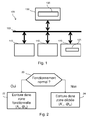
La
- un microprocesseur -ou unité de traitement- 110,
- des entrées/
sorties 115, - une ou plusieurs mémoires non volatile -ou mémoire morte- 120 par exemple ROM (acronyme de Read Only Memory en terminologie anglo-saxonne) stockant un système d'exploitation 125 et pouvant constituer un support au sens de l'invention, c'est-à-dire pouvant comprendre un programme informatique comprenant des instructions pour la mise en oeuvre du procédé selon l'invention dont des exemples sont décrits ci-après en référence aux
Figures 2 et3 ; cette mémoire non volatile peut également être une mémoire EEPROM (acronyme de Electrically Erasable Read Only Memory en terminologie anglo-saxonne) ou encore une mémoire Flash; - une mémoire vive 16 ou mémoire cache ou mémoire volatile par exemple RAM (acronyme de Random Access Memory en terminologie anglo-saxonne) comprenant des registres adaptés à l'enregistrement des variables et paramètres créés et modifiés au cours de l'exécution du programme précité ; lors de la mise en oeuvre de l'invention. Les codes d'instructions du programme stocké en mémoire non volatile (ex. EEPROM ou flash) sont chargés en mémoire RAM en vue d'être exécutés par le microprocesseur 110 ;
- une mémoire non-volatile 130, par exemple une mémoire EEPROM ou non réinscriptible (OTP) ou Flash, comportant une matrice de mémoire 135 et directement contrôlée
par le microprocesseur 110.
- a microprocessor -or processing unit-110,
- I /
O 115, - one or more nonvolatile memories - or read-only memory - 120 for example ROM (acronym for Read Only Memory in English terminology) storing an
operating system 125 and capable of constituting a medium within the meaning of the invention; that can include a computer program comprising instructions for carrying out the method according to the invention, examples of which are described below with reference toFigures 2 and3 ; this non-volatile memory can also be an EEPROM (acronym for Electrically Erasable Read Only Memory ) or a Flash memory; - a random access memory 16 or cache memory or volatile memory for example RAM (acronym for Random Access Memory in English terminology) comprising registers adapted to the recording of variables and parameters created and modified during the execution of the aforementioned program; during the implementation of the invention. The instruction codes of the program stored in non-volatile memory (eg EEPROM or flash) are loaded into RAM memory for execution by the
microprocessor 110; - a
non-volatile memory 130, for example an EEPROM or non-rewritable memory (OTP) or Flash, comprising amemory matrix 135 and directly controlled by themicroprocessor 110.
Dans un mode de réalisation particulier, un identifiant dont la lecture permet de repérer un fonctionnement anormal du microcircuit peut être retourné sur l'interface d'entrées/sorties 115, lors de la mise sous tension du microcircuit ou en réponse à une commande reçue sur cette interface 115, par exemple une commande APDU.In a particular embodiment, an identifier whose reading makes it possible to identify an abnormal operation of the microcircuit can be returned to the input /
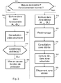
Dans son principe et tel qu'illustré sur la
En pratique cette étape consiste par exemple à mesurer un paramètre de fonctionnement du circuit afin de vérifier que sa valeur se situe dans une plage normale (c'est-à-dire caractéristique d'un fonctionnement normal du microcircuit) de valeurs.In practice, this step consists, for example, in measuring an operating parameter of the circuit in order to verify that its value is within a normal range (that is to say characteristic of a normal operation of the microcircuit) of values.
Le ou les paramètres mesurés sont par exemple :
- la température (une surchauffe par exemple peut révéler une attaque),
- la tension d'alimentation (une surtension par exemple peut être causée par un attaquant),
- les glitches, qui sont des variations de tension brusques et courtes généralement non perceptible par une simple mesure de la tension d'alimentation,
- la lumière, permettant par exemple de détecter une attaque par laser,
- la fréquence d'horloge (une modification de la fréquence d'horloge, parfois utilisée comme signal de base pour les calculs, peut-être être le fruit d'une attaque par faute).
- the temperature (overheating for example may reveal an attack),
- the supply voltage (an overvoltage for example can be caused by an attacker),
- the glitches, which are abrupt and short voltage variations generally not noticeable by a simple measurement of the supply voltage,
- light, for example to detect a laser attack,
- the clock frequency (a change in the clock frequency, sometimes used as a basic signal for calculations, may be the result of a fault attack).
L'étape de vérification peut également consister par exemple à vérifier une somme de contrôle ou de vérification (ou "Checksum" selon la terminologie anglo-saxonne), c'est-à-dire à vérifier que des données inscrites en mémoire sont bien cohérentes avec la somme de vérification associée à ces données.The verification step may also consist, for example, in checking a checksum or verification (or "checksum" in the English terminology), that is to say, in verifying that data entered in memory are indeed coherent with the checksum associated with these data.
En outre, il est aussi possible de vérifier si une variable présente bien certaines propriétés (e.g. parité, valeur). Cette étape peut également être basée sur la comparaison des résultats obtenus par deux mises en oeuvre d'un même algorithme.In addition, it is also possible to check if a variable has certain properties (eg parity, value). This step can also be based on the comparison of the results obtained by two implementations of the same algorithm.
Si l'étape de vérification (20) permet de conclure que le microcircuit fonctionne normalement, lorsque le processeur commande une écriture (22) d'une donnée An de n octets à l'adresse @A, celle-ci est exécutée normalement à l'adresse indiquée correspondant à une cellule de mémoire, par exemple la mémoire non-volatile 130, éventuellement découpée en zones (e.g. zone fonctionnelle où sont classiquement écrites les données, zone sécuritaire).If the verification step (20) makes it possible to conclude that the microcircuit is operating normally, when the processor controls a write (22) of a data item A n of n bytes to the address @ A , this is executed normally at the indicated address corresponding to a memory cell, for example the
Généralement, une telle écriture comporte un certain nombre d'étapes, classiquement :
- une étape d'effacement de la zone d'écriture fonctionnelle visée par l'adresse @A, lorsque le type de mémoire le permet (en particulier, les mémoires de type OTP pour One Time Programmable, ne peuvent pas être effacées)
- une étape de détermination d'au moins une somme de vérification (Checksum) à partir de la donnée An qui doit être écrite,
- une étape d'écriture de la donnée An et de chaque somme de vérification déterminée lors de l'étape de détermination,
- une étape de relecture de la donnée écrite An et de chaque somme de vérification, et
- une étape de détermination de la validité des sommes de vérification en refaisant, sur les données lues, une détermination de chaque somme de vérification correspondante et en la comparant avec la somme de vérification lue.
- a step of erasing the functional writing area targeted by the address @ A , when the type of memory allows it (in particular, the OTP memories for One Time Programmable, can not be erased)
- a step of determining at least one checksum (Checksum) from the data A n to be written,
- a step of writing the data A n and of each verification sum determined during the determination step,
- a step of reading the written data A n and of each checksum, and
- a step of determining the validity of the checksums by redoing, on the data read, a determination of each corresponding checksum and comparing it with the checksum read.
Certaines de ces étapes peuvent éventuellement être omises pour une écriture plus rapide.Some of these steps may possibly be omitted for faster writing.
En revanche, si l'étape de vérification (20) révèle un disfonctionnement du microcircuit, lorsque le processeur commande une écriture d'une donnée An de n octets à l'adresse @A, celle-ci est modifiée de façon à écrire (étape 24) une donnée A'n comportant le même nombre n d'octets à l'adresse @A'.On the other hand, if the verification step (20) reveals a dysfunction of the microcircuit, when the processor commands a writing of a data item A n of n bytes to the address @ A , the latter is modified so as to write ( step 24) a data A ' n having the same number n bytes at the address @ A' .
Bien entendu, l'écriture modifiée se déroule de manière strictement identique à une écriture normale dont les étapes classiques ont été décrites ci-avant. Par conséquent, cette écriture modifiée n'a pas d'impact supplémentaire sur le fonctionnement global du microcircuit, par rapport à une écriture normale. La modification concerne uniquement la nature de la donnée finalement écrite et l'adresse de l'écriture.Of course, the modified writing proceeds in exactly the same way as a normal writing whose conventional steps have been described above. Therefore, this modified write has no additional impact on the overall operation of the microcircuit, compared to a normal writing. The modification concerns only the nature of the data finally written and the address of the writing.
En particulier, la donnée A'n est obtenue en substituant un nombre n' d'octet(s) de la donnée An par un identifiant (ou trace) dont la lecture permet de repérer un fonctionnement anormal du microcircuit.In particular, the data A ' n is obtained by substituting a number n' of byte (s) of the data item A n by an identifier (or trace) whose reading makes it possible to identify abnormal operation of the microcircuit.
Par exemple, si la donnée An est constituée de 5 octets, la donnée A'n peut être constituée d'un premier octet reflétant par exemple une anomalie de température et des 4 derniers octets de la donnée An. Ainsi, dans cet exemple, les données An et A'n sont très proches en termes de contenu et font la même taille. Comme représenté sur la
De manière générale, plus les données An et A'n auront d'octets en commun, plus leur écriture aura une signature similaire, et donc moins elles seront discernables pour l'attaquant.In general, the more data A n and A ' n have bytes in common, the more their writing will have a similar signature, and therefore the less they will be discernable for the attacker.
L'écriture de la donnée A'n permet en outre de garder une trace de l'anomalie de fonctionnement, grâce à l'identifiant qu'elle comprend, préférentiellement en en-tête afin de faciliter la reconnaissance de l'anomalie lors d'une lecture ultérieure de la donnée (ce cas sera décrit en détail en référence à la
Dans un mode de réalisation préféré, la donnée A'n est écrite à une adresse @A' pointant dans une zone spécifique de la mémoire, dédiée à stocker au moins temporairement les données lorsqu'une anomalie est détectée.In a preferred embodiment, the data A ' n is written to an address @ A' pointing in a specific area of the memory, dedicated to at least temporarily storing the data when an anomaly is detected.
Ainsi, dans ce mode de réalisation, cette zone dédiée ne contient de données que lorsqu'un dysfonctionnement du microcircuit est détecté à l'étape 20.Thus, in this embodiment, this dedicated area contains data only when a malfunction of the microcircuit is detected in
Dans un mode de réalisation particulier, l'identifiant dont la lecture permet de repérer un fonctionnement anormal du microcircuit peut être retourné sur l'interface d'entrées/sorties 115 (voir
La
Des références sont faites à la
En variante, les écritures fonctionnelles pourraient viser différentes mémoires, préférentiellement de même type (e.g. OTP, EEPROM, Flash).As a variant, functional writes could target different memories, preferably of the same type (e.g. OTP, EEPROM, Flash).
Dans cet exemple, on mesure (étape 300) un paramètre P du microcircuit. A ce stade, on considère que la mémoire est vide (
Si la valeur mesurée de ce paramètre P est située dans une plage de valeurs caractéristiques du fonctionnement normal du microcircuit, une écriture 305 (similaire à l'étape 22 de la
Supposons maintenant que la valeur mesurée de ce paramètre P soit anormale, alors l'écriture est modifiée (étape 310 similaire à l'étape 24 de la
En particulier, l'écriture est modifiée sous deux aspects :
- la nature de la donnée finalement écrite (mais le nombre d'octets reste identique), celle-ci correspond à la donnée à écrire en fonctionnement normale dans laquelle un nombre n' d'octet(s), préférentiellement en en-tête, a été substitué par un identifiant ID du type d'anomalie, ici le paramètre P, et
- l'adresse de l'écriture, préférentiellement dans une zone dédiée différente de la zone fonctionnelle (où les données sont écrites en fonctionnement normal).
- the nature of the data finally written (but the number of bytes remains the same), this one corresponds to the data to be written in normal operation in which a number n 'of byte (s), preferentially in the header, has has been substituted by an identifier ID of the anomaly type, here the parameter P, and
- the address of the writing, preferably in a dedicated area different from the functional area (where the data are written in normal operation).
Mis à part ces deux aspects, l'écriture modifiée se déroule de manière strictement identique à une écriture normale dont les étapes classiques ont été décrites précédemment.Apart from these two aspects, the modified writing proceeds in exactly the same way as a normal writing whose conventional steps have been described previously.
Ainsi, comme représenté sur la
Après un certain temps, le microcircuit redémarre (étape 320). Ce redémarrage peut être provoqué par un utilisateur en coupant puis rétablissant l'alimentation de la carte à microcircuit par exemple. En variante, le microcircuit peut être redémarré périodiquement ou sous certaines conditions.After a while, the microcircuit restarts (step 320). This restart can be caused by a user by cutting and then restoring the power of the microcircuit card for example. Alternatively, the microcircuit can be restarted periodically or under certain conditions.
Au cours d'une étape 330 de consultation de la zone dédiée MA', la donnée A'n,ID est lue et au cours d'une étape 340, l'identifiant ID qu'elle contient est écrit dans la zone de mémoire sécuritaire MSECU.During a
De façon avantageuse, si l'identifiant est constitué par le ou les octet(s) en en-tête de la donnée, la lecture est facilité puisqu'il s'agit de lire simplement le ou les premiers octets de la donnée.Advantageously, if the identifier is constituted by the byte (s) in the header of the data, reading is facilitated since it is simply read the first byte or bytes of the data.
Le nombre d'octet(s) à lire peut par exemple être prédéterminé.The number of bytes (s) to be read may for example be predetermined.
A ce stade, et comme représenté sur la
Cette étape de consultation 330 peut être en variante initiée après un laps de temps prédéterminé (par exemple périodiquement), sans redémarrage du terminal, ou bien sur détection d'un évènement particulier, par exemple la valeur d'un compteur ayant atteint un seuil prédéterminé.This
Afin d'éviter que cet identifiant soit recopié une nouvelle fois dans la zone sécuritaire MSECU lors d'une consultation ultérieure de la zone de mémoire dédiée MA', le contenu de la mémoire dédiée MA' est effacé au cours d'une étape 350. La
Après un laps de temps prédéterminé, la zone de mémoire sécuritaire MSECU est à son tour consultée (étape 360). En variante, la zone de mémoire sécuritaire MSECU peut être consultée au démarrage du microcircuit, ou encore lorsqu'un évènement particulier est détecté.After a predetermined period of time, the safe memory zone M SECU is in turn consulted (step 360). In a variant, the safe memory zone M SECU can be consulted at the start of the microcircuit, or when a particular event is detected.
On rappelle que dans notre exemple, la zone de mémoire sécuritaire MSECU contient l'identifiant ID du paramètre P.Remember that in our example, the safe memory zone M SECU contains the identifier ID of the parameter P.
Lorsque le contenu de la zone sécuritaire MSECU rempli certaines conditions (test 370), par exemple lorsqu'elle contient un nombre donné d'identifiants, ou bien lorsqu'elle comprend un identifiant spécifique, par exemple un identifiant du paramètre P, alors une fonction de protection est mise en oeuvre.When the content of the safe zone M SECU fulfills certain conditions (test 370), for example when it contains a given number of identifiers, or when it comprises a specific identifier, for example an identifier of the parameter P, then a protection function is implemented.
Ainsi, une telle condition peut être du type 'si la tension d'alimentation est anormale, alors la fonction de protection est mise en oeuvre' ou encore 'si au moins trois paramètres sont défaillants, alors la fonction de protection est mise en oeuvre'.Thus, such a condition can be of the type 'if the supply voltage is abnormal, then the protection function is implemented' or 'if at least three parameters are faulty, then the protection function is implemented' .
Typiquement, cette fonction de protection peut être une fonction de mise hors service du microcircuit (e.g. fonction Killcard).Typically, this protection function can be a decommissioning function of the microcircuit (eg Killcard function).
En pratique, la mise en oeuvre d'une telle fonction de protection consiste à mettre à une valeur prédéterminée un drapeau de destruction (Killcard Flag) ayant pour effet, lors de sa lecture par le microprocesseur, par exemple la destruction immédiate des données contenues dans le microcircuit, et/ou le blocage du fonctionnement de celui-ci.In practice, the implementation of such a protection function consists in setting to a predetermined value a Killcard Flag having the effect, when read by the microprocessor, for example the immediate destruction of the data contained in the microcircuit, and / or the blocking of the operation thereof.
Si ces conditions ne sont pas remplies à l'étape 370, alors la fonction de protection n'est pas réalisée.If these conditions are not met in
Dans cet exemple de réalisation, le fonctionnement du circuit n'est vérifié qu'une seule fois. L'invention couvre cependant des modes dans lesquels plusieurs vérifications sont effectuées, et plusieurs étapes d'écritures sont réalisées. En particulier, si les écritures normales peuvent viser plusieurs zones de mémoire différentes et même plusieurs mémoires, les écritures en fonctionnement anormal visent toujours la zone dédiée, par exemple située à l'intérieur d'une seule page de mémoire.In this embodiment, the operation of the circuit is checked only once. The invention however covers modes in which several checks are made, and several steps of writing are performed. In particular, if the normal writes can aim at several different memory areas and even several memories, the writes in abnormal operation always target the dedicated area, for example located inside a single page of memory.
Préférentiellement, lorsque plusieurs anomalies sont détectées avant que la zone dédiée ne soit consultée, les écritures des traces correspondantes sont réalisées à des adresses différentes de la zone dédiée, de sorte à ne pas substituer une trace par une autre. Ainsi, cela permet de garder une trace de toutes les anomalies détectées avant la consultation de la zone dédiée.Preferably, when several anomalies are detected before the dedicated zone is consulted, the writes of the corresponding traces are made at different addresses of the dedicated zone, so as not to substitute a trace by another. Thus, it makes it possible to keep a record of all the anomalies detected before the consultation of the dedicated zone.
Dans un mode de réalisation particulier, l'identifiant dont la lecture permet de repérer un fonctionnement anormal du microcircuit peut être retourné sur l'interface d'entrées/sorties 115 (voir
Les exemples qui précèdent ne sont que des modes de réalisation de l'invention qui ne s'y limite pas.The foregoing examples are only embodiments of the invention which is not limited thereto.
Claims (21)
et lors de l'autre étape de vérification, si le microcircuit ne fonctionne pas normalement, le procédé comprend une étape d'écriture d'une quatrième donnée à une quatrième adresse pointant vers ladite zone de mémoire dédiée, ladite quatrième donnée étant obtenue en substituant une partie de la troisième donnée qui serait écrite en fonctionnement normal par un identifiant du fonctionnement anormal.
and in the other verification step, if the microcircuit does not operate normally, the method comprises a step of writing a fourth datum to a fourth address pointing to said dedicated memory area, said fourth datum being obtained by substituting part of the third data which would be written in normal operation by an identifier of abnormal operation.
Applications Claiming Priority (1)
| Application Number | Priority Date | Filing Date | Title |
|---|---|---|---|
| FR1359806A FR3011658B1 (en) | 2013-10-09 | 2013-10-09 | METHOD IN MICROCIRCUIT AND ASSOCIATED DEVICE |
Publications (2)
| Publication Number | Publication Date |
|---|---|
| EP2860669A1 true EP2860669A1 (en) | 2015-04-15 |
| EP2860669B1 EP2860669B1 (en) | 2020-11-25 |
Family
ID=50289734
Family Applications (1)
| Application Number | Title | Priority Date | Filing Date |
|---|---|---|---|
| EP14188000.5A Active EP2860669B1 (en) | 2013-10-09 | 2014-10-07 | Method implemented in a microcircuit and related device |
Country Status (2)
| Country | Link |
|---|---|
| EP (1) | EP2860669B1 (en) |
| FR (1) | FR3011658B1 (en) |
Cited By (1)
| Publication number | Priority date | Publication date | Assignee | Title |
|---|---|---|---|---|
| FR3045862A1 (en) * | 2015-12-17 | 2017-06-23 | Oberthur Technologies | METHOD FOR WRITING IN A NON-VOLATILE MEMORY, METHOD FOR READING IN A NON-VOLATILE MEMORY AND METHOD IMPLEMENTED IN AN ELECTRONIC ENTITY |
Citations (2)
| Publication number | Priority date | Publication date | Assignee | Title |
|---|---|---|---|---|
| US7039815B1 (en) * | 1999-10-01 | 2006-05-02 | Giesecke & Devrient Gmbh | Method for protecting a data memory |
| FR2935823A1 (en) | 2008-09-11 | 2010-03-12 | Oberthur Technologies | METHOD AND DEVICE FOR PROTECTING A MICROCIRCUIT AGAINST ATTACKS. |
-
2013
- 2013-10-09 FR FR1359806A patent/FR3011658B1/en active Active
-
2014
- 2014-10-07 EP EP14188000.5A patent/EP2860669B1/en active Active
Patent Citations (3)
| Publication number | Priority date | Publication date | Assignee | Title |
|---|---|---|---|---|
| US7039815B1 (en) * | 1999-10-01 | 2006-05-02 | Giesecke & Devrient Gmbh | Method for protecting a data memory |
| FR2935823A1 (en) | 2008-09-11 | 2010-03-12 | Oberthur Technologies | METHOD AND DEVICE FOR PROTECTING A MICROCIRCUIT AGAINST ATTACKS. |
| EP2164031B1 (en) * | 2008-09-11 | 2012-07-25 | Oberthur Technologies | Method and device for protecting an integrated circuit against attacks |
Cited By (1)
| Publication number | Priority date | Publication date | Assignee | Title |
|---|---|---|---|---|
| FR3045862A1 (en) * | 2015-12-17 | 2017-06-23 | Oberthur Technologies | METHOD FOR WRITING IN A NON-VOLATILE MEMORY, METHOD FOR READING IN A NON-VOLATILE MEMORY AND METHOD IMPLEMENTED IN AN ELECTRONIC ENTITY |
Also Published As
| Publication number | Publication date |
|---|---|
| FR3011658A1 (en) | 2015-04-10 |
| EP2860669B1 (en) | 2020-11-25 |
| FR3011658B1 (en) | 2017-02-10 |
Similar Documents
| Publication | Publication Date | Title |
|---|---|---|
| EP2164031B1 (en) | Method and device for protecting an integrated circuit against attacks | |
| EP1904946B1 (en) | Detection of faults during a long perturbation | |
| WO2006045924A1 (en) | Protection against attacks by generation of errors on jump instructions | |
| CA2575143C (en) | Data processing method and device | |
| FR2894709A1 (en) | "DETECTOR OF ABNORMAL DESTRUCTION OF MEMORY SECTOR" | |
| EP2724237B1 (en) | Method of managing the endurance of non-volatile memories | |
| EP2860669B1 (en) | Method implemented in a microcircuit and related device | |
| EP3391228B1 (en) | Method for writing in a non-volatile memory of an electronic entity, and related electronic entity | |
| EP2860668B1 (en) | Method and device for performing a function by a microcircuit | |
| EP3042334B1 (en) | Method of setting up safety means depending on a trust indicia varying before and after command execution in an electronic device with memory, and device for implementing said method | |
| EP1715436A2 (en) | Protection of program execution performed by an integrated circuit or the data stored in this circuit | |
| FR3011650A1 (en) | METHOD AND DEVICE FOR REALIZING FUNCTION BY A MICROCIRCUIT | |
| EP2229648B1 (en) | Method for secure data transfer | |
| EP2466506A1 (en) | Dynamic method for verifying the integrity of the execution of executable code | |
| FR3011657A1 (en) | METHOD USED BY A PROCESSOR AND ASSOCIATED ELECTRONIC ENTITY | |
| EP3422232B1 (en) | Method for protecting an electronic device running a program against fault-injection attacks | |
| WO2008096076A2 (en) | Secured electronic systems, securing methods and uses of such systems | |
| FR3068152B1 (en) | METHOD FOR PROTECTING AN ELECTRONIC DEVICE EXECUTING A PROGRAM AGAINST FAULT INJECTION ATTACKS | |
| EP3203405B1 (en) | Method for executing instructions of object-oriented applications by an interpreter | |
| FR3080474A1 (en) | METHOD FOR CONTROLLING CONTROLS IMPLEMENTED BY A DEVICE SUCH AS A CHIP CARD, AND DEVICE. | |
| EP4032000A1 (en) | System on a chip and method guaranteeing the freshness of the data stored in an external memory | |
| FR2980600A1 (en) | Method for securing software application having conditional statement, involves modifying intermediate file by adding redundancy conditional statement determined based on state of Boolean variable and instruction |
Legal Events
| Date | Code | Title | Description |
|---|---|---|---|
| PUAI | Public reference made under article 153(3) epc to a published international application that has entered the european phase |
Free format text: ORIGINAL CODE: 0009012 |
|
| 17P | Request for examination filed |
Effective date: 20141007 |
|
| AK | Designated contracting states |
Kind code of ref document: A1 Designated state(s): AL AT BE BG CH CY CZ DE DK EE ES FI FR GB GR HR HU IE IS IT LI LT LU LV MC MK MT NL NO PL PT RO RS SE SI SK SM TR |
|
| AX | Request for extension of the european patent |
Extension state: BA ME |
|
| R17P | Request for examination filed (corrected) |
Effective date: 20150917 |
|
| RBV | Designated contracting states (corrected) |
Designated state(s): AL AT BE BG CH CY CZ DE DK EE ES FI FR GB GR HR HU IE IS IT LI LT LU LV MC MK MT NL NO PL PT RO RS SE SI SK SM TR |
|
| RAP1 | Party data changed (applicant data changed or rights of an application transferred) |
Owner name: IDEMIA FRANCE |
|
| GRAP | Despatch of communication of intention to grant a patent |
Free format text: ORIGINAL CODE: EPIDOSNIGR1 |
|
| STAA | Information on the status of an ep patent application or granted ep patent |
Free format text: STATUS: GRANT OF PATENT IS INTENDED |
|
| INTG | Intention to grant announced |
Effective date: 20200514 |
|
| GRAS | Grant fee paid |
Free format text: ORIGINAL CODE: EPIDOSNIGR3 |
|
| GRAA | (expected) grant |
Free format text: ORIGINAL CODE: 0009210 |
|
| STAA | Information on the status of an ep patent application or granted ep patent |
Free format text: STATUS: THE PATENT HAS BEEN GRANTED |
|
| AK | Designated contracting states |
Kind code of ref document: B1 Designated state(s): AL AT BE BG CH CY CZ DE DK EE ES FI FR GB GR HR HU IE IS IT LI LT LU LV MC MK MT NL NO PL PT RO RS SE SI SK SM TR |
|
| RAP1 | Party data changed (applicant data changed or rights of an application transferred) |
Owner name: IDEMIA FRANCE |
|
| REG | Reference to a national code |
Ref country code: GB Ref legal event code: FG4D Free format text: NOT ENGLISH |
|
| REG | Reference to a national code |
Ref country code: CH Ref legal event code: EP |
|
| REG | Reference to a national code |
Ref country code: AT Ref legal event code: REF Ref document number: 1339139 Country of ref document: AT Kind code of ref document: T Effective date: 20201215 |
|
| REG | Reference to a national code |
Ref country code: DE Ref legal event code: R096 Ref document number: 602014072637 Country of ref document: DE |
|
| REG | Reference to a national code |
Ref country code: IE Ref legal event code: FG4D Free format text: LANGUAGE OF EP DOCUMENT: FRENCH |
|
| REG | Reference to a national code |
Ref country code: NL Ref legal event code: MP Effective date: 20201125 |
|
| PG25 | Lapsed in a contracting state [announced via postgrant information from national office to epo] |
Ref country code: GR Free format text: LAPSE BECAUSE OF FAILURE TO SUBMIT A TRANSLATION OF THE DESCRIPTION OR TO PAY THE FEE WITHIN THE PRESCRIBED TIME-LIMIT Effective date: 20210226 Ref country code: PT Free format text: LAPSE BECAUSE OF FAILURE TO SUBMIT A TRANSLATION OF THE DESCRIPTION OR TO PAY THE FEE WITHIN THE PRESCRIBED TIME-LIMIT Effective date: 20210325 Ref country code: NO Free format text: LAPSE BECAUSE OF FAILURE TO SUBMIT A TRANSLATION OF THE DESCRIPTION OR TO PAY THE FEE WITHIN THE PRESCRIBED TIME-LIMIT Effective date: 20210225 Ref country code: RS Free format text: LAPSE BECAUSE OF FAILURE TO SUBMIT A TRANSLATION OF THE DESCRIPTION OR TO PAY THE FEE WITHIN THE PRESCRIBED TIME-LIMIT Effective date: 20201125 Ref country code: FI Free format text: LAPSE BECAUSE OF FAILURE TO SUBMIT A TRANSLATION OF THE DESCRIPTION OR TO PAY THE FEE WITHIN THE PRESCRIBED TIME-LIMIT Effective date: 20201125 |
|
| PG25 | Lapsed in a contracting state [announced via postgrant information from national office to epo] |
Ref country code: BG Free format text: LAPSE BECAUSE OF FAILURE TO SUBMIT A TRANSLATION OF THE DESCRIPTION OR TO PAY THE FEE WITHIN THE PRESCRIBED TIME-LIMIT Effective date: 20210225 Ref country code: SE Free format text: LAPSE BECAUSE OF FAILURE TO SUBMIT A TRANSLATION OF THE DESCRIPTION OR TO PAY THE FEE WITHIN THE PRESCRIBED TIME-LIMIT Effective date: 20201125 Ref country code: PL Free format text: LAPSE BECAUSE OF FAILURE TO SUBMIT A TRANSLATION OF THE DESCRIPTION OR TO PAY THE FEE WITHIN THE PRESCRIBED TIME-LIMIT Effective date: 20201125 Ref country code: IS Free format text: LAPSE BECAUSE OF FAILURE TO SUBMIT A TRANSLATION OF THE DESCRIPTION OR TO PAY THE FEE WITHIN THE PRESCRIBED TIME-LIMIT Effective date: 20210325 Ref country code: LV Free format text: LAPSE BECAUSE OF FAILURE TO SUBMIT A TRANSLATION OF THE DESCRIPTION OR TO PAY THE FEE WITHIN THE PRESCRIBED TIME-LIMIT Effective date: 20201125 |
|
| REG | Reference to a national code |
Ref country code: LT Ref legal event code: MG9D |
|
| PG25 | Lapsed in a contracting state [announced via postgrant information from national office to epo] |
Ref country code: HR Free format text: LAPSE BECAUSE OF FAILURE TO SUBMIT A TRANSLATION OF THE DESCRIPTION OR TO PAY THE FEE WITHIN THE PRESCRIBED TIME-LIMIT Effective date: 20201125 |
|
| PG25 | Lapsed in a contracting state [announced via postgrant information from national office to epo] |
Ref country code: CZ Free format text: LAPSE BECAUSE OF FAILURE TO SUBMIT A TRANSLATION OF THE DESCRIPTION OR TO PAY THE FEE WITHIN THE PRESCRIBED TIME-LIMIT Effective date: 20201125 Ref country code: EE Free format text: LAPSE BECAUSE OF FAILURE TO SUBMIT A TRANSLATION OF THE DESCRIPTION OR TO PAY THE FEE WITHIN THE PRESCRIBED TIME-LIMIT Effective date: 20201125 Ref country code: SM Free format text: LAPSE BECAUSE OF FAILURE TO SUBMIT A TRANSLATION OF THE DESCRIPTION OR TO PAY THE FEE WITHIN THE PRESCRIBED TIME-LIMIT Effective date: 20201125 Ref country code: SK Free format text: LAPSE BECAUSE OF FAILURE TO SUBMIT A TRANSLATION OF THE DESCRIPTION OR TO PAY THE FEE WITHIN THE PRESCRIBED TIME-LIMIT Effective date: 20201125 Ref country code: RO Free format text: LAPSE BECAUSE OF FAILURE TO SUBMIT A TRANSLATION OF THE DESCRIPTION OR TO PAY THE FEE WITHIN THE PRESCRIBED TIME-LIMIT Effective date: 20201125 Ref country code: LT Free format text: LAPSE BECAUSE OF FAILURE TO SUBMIT A TRANSLATION OF THE DESCRIPTION OR TO PAY THE FEE WITHIN THE PRESCRIBED TIME-LIMIT Effective date: 20201125 |
|
| REG | Reference to a national code |
Ref country code: DE Ref legal event code: R097 Ref document number: 602014072637 Country of ref document: DE |
|
| PG25 | Lapsed in a contracting state [announced via postgrant information from national office to epo] |
Ref country code: DK Free format text: LAPSE BECAUSE OF FAILURE TO SUBMIT A TRANSLATION OF THE DESCRIPTION OR TO PAY THE FEE WITHIN THE PRESCRIBED TIME-LIMIT Effective date: 20201125 |
|
| REG | Reference to a national code |
Ref country code: AT Ref legal event code: UEP Ref document number: 1339139 Country of ref document: AT Kind code of ref document: T Effective date: 20201125 |
|
| PLBE | No opposition filed within time limit |
Free format text: ORIGINAL CODE: 0009261 |
|
| STAA | Information on the status of an ep patent application or granted ep patent |
Free format text: STATUS: NO OPPOSITION FILED WITHIN TIME LIMIT |
|
| PG25 | Lapsed in a contracting state [announced via postgrant information from national office to epo] |
Ref country code: IT Free format text: LAPSE BECAUSE OF FAILURE TO SUBMIT A TRANSLATION OF THE DESCRIPTION OR TO PAY THE FEE WITHIN THE PRESCRIBED TIME-LIMIT Effective date: 20201125 Ref country code: NL Free format text: LAPSE BECAUSE OF FAILURE TO SUBMIT A TRANSLATION OF THE DESCRIPTION OR TO PAY THE FEE WITHIN THE PRESCRIBED TIME-LIMIT Effective date: 20201125 Ref country code: AL Free format text: LAPSE BECAUSE OF FAILURE TO SUBMIT A TRANSLATION OF THE DESCRIPTION OR TO PAY THE FEE WITHIN THE PRESCRIBED TIME-LIMIT Effective date: 20201125 |
|
| 26N | No opposition filed |
Effective date: 20210826 |
|
| PG25 | Lapsed in a contracting state [announced via postgrant information from national office to epo] |
Ref country code: ES Free format text: LAPSE BECAUSE OF FAILURE TO SUBMIT A TRANSLATION OF THE DESCRIPTION OR TO PAY THE FEE WITHIN THE PRESCRIBED TIME-LIMIT Effective date: 20201125 Ref country code: SI Free format text: LAPSE BECAUSE OF FAILURE TO SUBMIT A TRANSLATION OF THE DESCRIPTION OR TO PAY THE FEE WITHIN THE PRESCRIBED TIME-LIMIT Effective date: 20201125 |
|
| REG | Reference to a national code |
Ref country code: CH Ref legal event code: PL |
|
| PG25 | Lapsed in a contracting state [announced via postgrant information from national office to epo] |
Ref country code: IS Free format text: LAPSE BECAUSE OF FAILURE TO SUBMIT A TRANSLATION OF THE DESCRIPTION OR TO PAY THE FEE WITHIN THE PRESCRIBED TIME-LIMIT Effective date: 20210325 |
|
| REG | Reference to a national code |
Ref country code: BE Ref legal event code: MM Effective date: 20211031 |
|
| GBPC | Gb: european patent ceased through non-payment of renewal fee |
Effective date: 20211007 |
|
| PG25 | Lapsed in a contracting state [announced via postgrant information from national office to epo] |
Ref country code: MC Free format text: LAPSE BECAUSE OF FAILURE TO SUBMIT A TRANSLATION OF THE DESCRIPTION OR TO PAY THE FEE WITHIN THE PRESCRIBED TIME-LIMIT Effective date: 20201125 |
|
| PG25 | Lapsed in a contracting state [announced via postgrant information from national office to epo] |
Ref country code: LU Free format text: LAPSE BECAUSE OF NON-PAYMENT OF DUE FEES Effective date: 20211007 Ref country code: GB Free format text: LAPSE BECAUSE OF NON-PAYMENT OF DUE FEES Effective date: 20211007 Ref country code: BE Free format text: LAPSE BECAUSE OF NON-PAYMENT OF DUE FEES Effective date: 20211031 |
|
| PG25 | Lapsed in a contracting state [announced via postgrant information from national office to epo] |
Ref country code: LI Free format text: LAPSE BECAUSE OF NON-PAYMENT OF DUE FEES Effective date: 20211031 Ref country code: CH Free format text: LAPSE BECAUSE OF NON-PAYMENT OF DUE FEES Effective date: 20211031 |
|
| PG25 | Lapsed in a contracting state [announced via postgrant information from national office to epo] |
Ref country code: IE Free format text: LAPSE BECAUSE OF NON-PAYMENT OF DUE FEES Effective date: 20211007 |
|
| PG25 | Lapsed in a contracting state [announced via postgrant information from national office to epo] |
Ref country code: HU Free format text: LAPSE BECAUSE OF FAILURE TO SUBMIT A TRANSLATION OF THE DESCRIPTION OR TO PAY THE FEE WITHIN THE PRESCRIBED TIME-LIMIT; INVALID AB INITIO Effective date: 20141007 |
|
| P01 | Opt-out of the competence of the unified patent court (upc) registered |
Effective date: 20230428 |
|
| PG25 | Lapsed in a contracting state [announced via postgrant information from national office to epo] |
Ref country code: CY Free format text: LAPSE BECAUSE OF FAILURE TO SUBMIT A TRANSLATION OF THE DESCRIPTION OR TO PAY THE FEE WITHIN THE PRESCRIBED TIME-LIMIT Effective date: 20201125 |
|
| PGFP | Annual fee paid to national office [announced via postgrant information from national office to epo] |
Ref country code: FR Payment date: 20230920 Year of fee payment: 10 |
|
| PGFP | Annual fee paid to national office [announced via postgrant information from national office to epo] |
Ref country code: DE Payment date: 20230920 Year of fee payment: 10 Ref country code: AT Payment date: 20230921 Year of fee payment: 10 |